viterbi decoder: presentation #9 m1 overall project objective: design a high speed viterbi decoder...
Post on 22-Dec-2015
222 views
TRANSCRIPT

Viterbi Decoder: Presentation #9
M1
Overall Project Objective:
Design a high speed Viterbi Decoder
Stage 9: 29nd Mar. 2004
Chip Level Simulation
Design Manager: Yaping Zhan
Omar Ahmad
Prateek Goenka
Saim Qidwai
Lingyan Sun
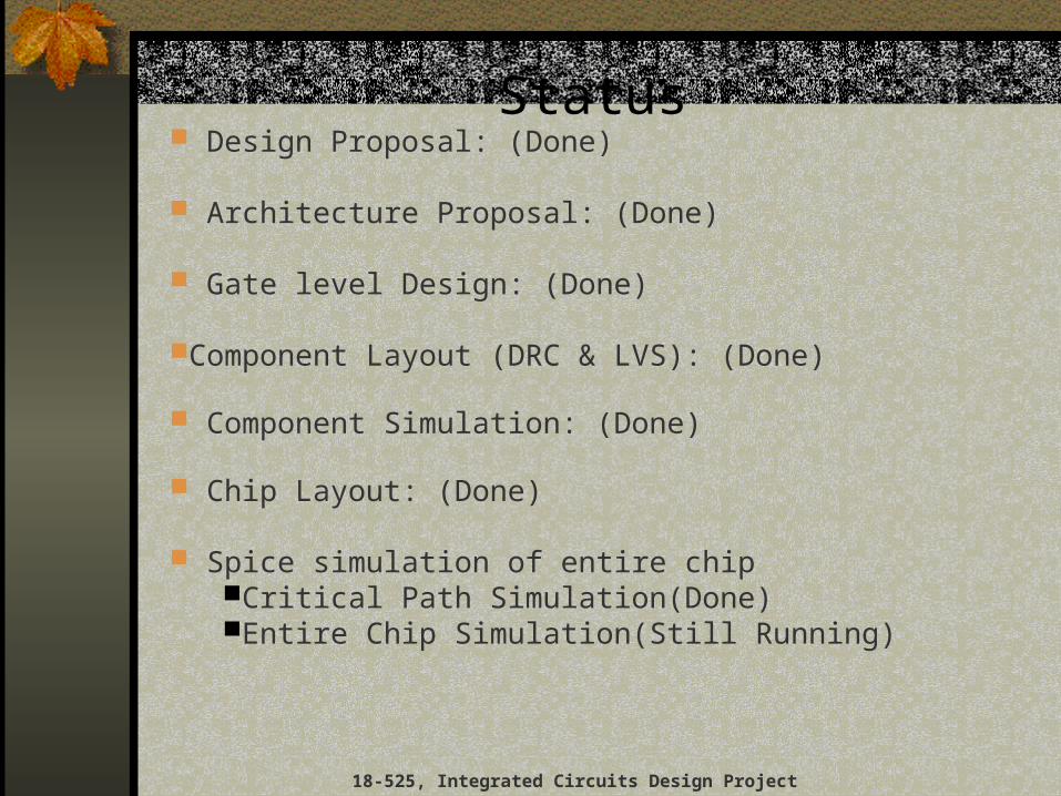
Status
18-525, Integrated Circuits Design Project
Design Proposal: (Done)
Architecture Proposal: (Done)
Gate level Design: (Done)
Component Layout (DRC & LVS): (Done)
Component Simulation: (Done)
Chip Layout: (Done)
Spice simulation of entire chip Critical Path Simulation(Done)Entire Chip Simulation(Still Running)
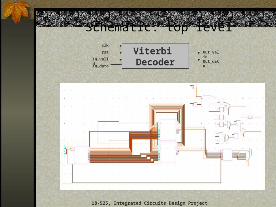
Schematic: top level
18-525, Integrated Circuits Design Project
Viterbi Decoder
clk
rst
In_valid
In_data
Out_valid
Out_data

18-525, Integrated Circuits Design Project
Layout – Entire Chip

Critical Path Extraction
18-525, Integrated Circuits Design Project
DFF
MUX
COMP
+ +
DFF
+ +
+

Input Pattern Selection
Input_0 Input_1
011001 011001
010000 010000
001001 001001
000001 000001
000000 000000
Find all possible input patterns
18-525, Integrated Circuits Design Project

Input Pattern Selection
DFF
MUX
COMP
+ +
Worst case pattern for adder: 011001 and 001001
Worst Case pattern for Comp: two Inputs are the same: 011001 vs. 011001
100111 + 011001
000000
Decision : Use input pattern 011001 and 001001 for both adders
18-525, Integrated Circuits Design Project

Waveform
Testing Speed: 500 MHz
18-525, Integrated Circuits Design Project
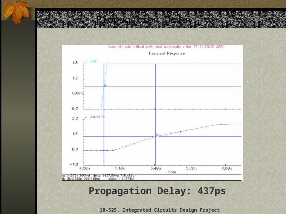
Propagation Delay
18-525, Integrated Circuits Design Project
Propagation Delay: 437ps

Rising Time
18-525, Integrated Circuits Design Project
Rising Time: 750 ps

ACS Simulation: Got DC to GND errors
Whole Chip Simulation: Still Running
18-525, Integrated Circuits Design Project

18-525, Integrated Circuits Design Project
Questions