vivado design suite tutorial - xilinx · vivado design suite tutorial model-based dsp design using...
TRANSCRIPT

Vivado Design Suite Tutorial
Model-Based DSP Design Using
System Generator
UG948 (v2016.3) October 28, 2016
UG948 (v2016.4) November 30, 2016
This tutorial was validated with 2016.3. Minor procedural differences might be required when using laterreleases.

Revision History
Date Version Changes
10/28/2016 2016.3 Recaptured screen displays throughout manual to reflect changes to
GUI or changes in results displayed.
In Lab 2: Working with Data Types, added procedural step to specify the
number of input ports on the Scope block, allowing the block to be
properly connected to other blocks in the Simulink model.
06/20/2016 2016.2 No technical updates. Re-release only.
05/23/2016 2016.1 Recaptured screen displays throughout manual to reflect changes to
GUI or changes in results displayed.
In design used in Lab 1_1 and 1_2, replaced FIR Compiler 7.2 block with
Digital FIR Filter block.
11/30/2016: Released with Vivado® Design Suite 2016.4 without changes from 2016.3.
Model-Based DSP Design Using System Generator 3 UG948 (v2016.3) October 28, 2016 www.xilinx.com
Table of Contents
Revision History ..................................................................................................................................................2
System Generator for DSP Overview ......................................................................................................................5
Introduction ........................................................................................................................................................5
Software Requirements ......................................................................................................................................7
Configuring MATLAB to the Vivado® Design Suite .............................................................................................7
Locating and Preparing the Tutorial Design Files ...............................................................................................8
Lab 1: Introduction to System Generator ...............................................................................................................9
Introduction ........................................................................................................................................................9
Step 1: Creating a Design in an FPGA .............................................................................................................. 10
Step 2: Creating an Optimized Design in an FPGA .......................................................................................... 26
Step 3: Creating a Design Using Discrete Resources ....................................................................................... 30
Summary .......................................................................................................................................................... 40
Lab 2: Working with Data Types .......................................................................................................................... 41
Introduction ..................................................................................................................................................... 41
Step 1: Designing with Floating-Point Data Types ........................................................................................... 42
Step 2: Designing with Fixed-Point Data Types ............................................................................................... 46
Summary .......................................................................................................................................................... 53
Lab 3: Working with Multi-Rate Systems ............................................................................................................ 54
Introduction ..................................................................................................................................................... 54
Step 1: Creating Clock Domain Hierarchies ..................................................................................................... 54
Step 2: Creating Asynchronous Channels ........................................................................................................ 58
Step 3: Specifying Clock Domains .................................................................................................................... 63
Summary .......................................................................................................................................................... 68
Lab 4: Working with Workspace Variables .......................................................................................................... 69
Introduction ..................................................................................................................................................... 69
Step 1: Using Workspace Variables ................................................................................................................. 70
Summary .......................................................................................................................................................... 75
Send FeedbackUG948 (v2016.4) November 30, 2016
Model-Based DSP Design Using System Generator 4 UG948 (v2016.3) October 28, 2016 www.xilinx.com
Lab 5: Modeling Control with M-Code ................................................................................................................ 76
Introduction ..................................................................................................................................................... 76
Step 1: Designing Padding Logic ...................................................................................................................... 76
Summary .......................................................................................................................................................... 80
Lab 6: Modeling Blocks with HDL ........................................................................................................................ 81
Introduction ..................................................................................................................................................... 81
Step 1: Import RTL as a Black Box .................................................................................................................... 81
Summary .......................................................................................................................................................... 87
Lab 7: Modeling Blocks with C Code .................................................................................................................... 88
Introduction ..................................................................................................................................................... 88
Step 1: Creating a System Generator Package from Vivado HLS .................................................................... 89
Step 2: Including a Vivado HLS Package in a System Generator Design .......................................................... 92
Summary .......................................................................................................................................................... 96
Lab 8: Using AXI Interfaces and IP Integrator ...................................................................................................... 97
Introduction ..................................................................................................................................................... 97
Step 1: Review the AXI Interfaces.................................................................................................................... 98
Step 2: Create a Vivado Project using System Generator IP ........................................................................... 99
Step 3: Create a Design in IP Integrator (IPI) ................................................................................................. 101
Step 4: Implement the Design ....................................................................................................................... 108
Summary ........................................................................................................................................................ 109
Lab 9: Using a System Generator Design with a Zynq-7000 AP SoC ................................................................. 110
Introduction ................................................................................................................................................... 110
Step 1: Review the AXI4-Lite Interface Drivers.............................................................................................. 111
Step 2: Developing Software and Running it on the ZYNQ-7000 System ..................................................... 114
Summary ........................................................................................................................................................ 120
Legal Notices ...................................................................................................................................................... 121
Please Read: Important Legal Notices ........................................................................................................... 121
Send FeedbackUG948 (v2016.4) November 30, 2016
Model-Based DSP Design Using System Generator 5 UG948 (v2016.3) October 28, 2016 www.xilinx.com
System Generator for DSP Overview
Introduction System Generator for DSP is a design tool in the Vivado® Design Suite that enables you to use the
MathWorks® model-based Simulink® design environment for FPGA design. Previous experience with
Xilinx® FPGA devices or RTL design methodologies is not required when using System Generator.
Designs are captured in the Simulink™ modeling environment using a Xilinx-specific block set.
Downstream FPGA steps including RTL synthesis and implementation (where the gate level design is
placed and routed in the FPGA) are automatically performed to produce an FPGA programming
bitstream.
Over 80 building blocks are included in the Xilinx-specific DSP block set for Simulink. These blocks
include common building blocks such as adders, multipliers and registers. Also included are complex
DSP building blocks such as forward-error-correction blocks, FFTs, filters, and memories. These complex
blocks leverage Xilinx LogiCORE™ IP to produce optimized results for the selected target device.
VIDEO: The Vivado Design Suite Quick Take Video Tutorial: System Generator Multiple
Clock Domains describes how to use Multiple Clock Domains within System Generator, making it
possible to implement complex DSP systems.
VIDEO: The Vivado Design Suite QuickTake Video Tutorial: Generating Vivado HLS block
for use in System Generator for DSP describes how to generate a Vivado HLS IP block for use in
System Generator, and ends with a summary of how the Vivado HLS block can be used in your
System Generator design.
VIDEO: The Vivado Design Suite Quick Take Video: Using Vivado HLS C/C++/System C
block in System Generator describes how to incorporate your Vivado HLS design as an IP block
into System Generator for DSP.
Send FeedbackUG948 (v2016.4) November 30, 2016
System Generator for DSP Overview
Model-Based DSP Design Using System Generator 6 UG948 (v2016.3) October 28, 2016 www.xilinx.com
VIDEO: The Vivado Design Suite Quick Take Video: Specifying AXI4-Lite Interfaces for your
Vivado System Generator Design describes how System Generator provides AXI4-Lite
abstraction making it possible to incorporate a DSP design into an embedded system. Full support
includes integration into the IP Catalog, interface connectivity automation, and software APIs.
VIDEO: The Vivado Design Suite QuickTake Video Tutorial: Using Hardware Co-Simulation
with Vivado System Generator for DSP describes how to use Point-to-Point Ethernet Hardware
Co-Simulation with Vivado System Generator for DSP. Hardware co-simulation makes it possible to
incorporate a design running in an FPGA directly into a Simulink simulation.
In this tutorial, you will do the following:
Lab 1: Understand how to create and validate a model using System Generator, synthesize the
model into FPGA hardware, and then create a more optimal hardware version of the design.
Lab 2: Learn how fixed-point data types can be used to trade off accuracy against hardware area
and performance.
Lab 3: Learn how to create an efficient design using multiple clock domains.
Lab 4: Make use of workspace variables to easily parameterize your models.
Lab 5: Model a control system using M-code.
Lab 6: Learn how to incorporate existing RTL designs, written in Verilog or VHDL, into your
design.
Lab 7: Import C/C++ source files into a System Generator model by leveraging the tool
integration with Vivado High-Level Synthesis (HLS).
Lab 8: Use AXI interfaces and Vivado IP integrator to easily include your model into a larger
design.
Lab 9: Integrate your design into a larger system and operate the design under CPU control.
Send FeedbackUG948 (v2016.4) November 30, 2016

System Generator for DSP Overview
Model-Based DSP Design Using System Generator 7 UG948 (v2016.3) October 28, 2016 www.xilinx.com
Software Requirements The lab exercises in this tutorial require the installation of MATLAB R2015b, R2015a, R2014b, or R2014.a.
See the Vivado Design Suite User Guide: Release Notes, Installation, and Licensing (UG973) for a
complete list and description of the system and software requirements.
Configuring MATLAB to the Vivado® Design Suite Before you begin, you should verify that MATLAB is configured to the Vivado Design Suite. Do the
following:
1. Configure MATLAB.
On Windows systems:
a. Select Start > All Programs > Xilinx Design Tools > Vivado 2016.3 > System Generator
> System Generator 2016.3 MATLAB Configurator.
IMPORTANT: On Windows systems you may need to launch the MATLAB configurator
as Administrator. When MATLAB Configurator is selected in the menu, use the mouse
right-click to select Run as Administrator.
Figure 1: Select MATLAB Installation
b. Click the check box of the version of MATLAB you want to configure and then click OK.
On Linux systems:
Launching System Generator under Linux is handled via a shell script called sysgen located in the
<Vivado install dir>/bin directory. Before launching this script, you must make sure the
Send FeedbackUG948 (v2016.4) November 30, 2016
System Generator for DSP Overview
Model-Based DSP Design Using System Generator 8 UG948 (v2016.3) October 28, 2016 www.xilinx.com
MATLAB executable can be found in your Linux system’s $PATH environment variable. When you
execute the sysgen script, it will launch the first MATLAB executable found in $PATH and attach
System Generator to that session of MATLAB. Also, the sysgen shell script supports all the options
that MATLAB supports and all options can be passed as command line arguments to the sysgen
script.
When the System Generator opens, you can confirm the version of MATLAB to which System
Generator is attached by entering the version command in the MATLAB Command Window.
>> version
ans =
8.6.0.267246 (R2015b)
Locating and Preparing the Tutorial Design Files There are separate project files and sources for each of the labs in this tutorial. You can find the design
files for this tutorial under Error! Hyperlink reference not valid. on the www.xilinx.com website.
1. Download the Reference Design Files (ug948-design-files.zip) from the Xilinx website.
2. Extract the zip file contents into any write-accessible location on your hard drive or network
location.
RECOMMENDED: You will modify the tutorial design data while working through this
tutorial. You should use a new copy of the SysGen_Tutorial directory extracted from
ug948-design-files.zip each time you start this tutorial.
TIP: This document assumes the tutorial files are stored at C:\SysGen_Tutorial. All
pathnames and figures in this document refer to this pathname. If you choose to store
the tutorial in another location, adjust the pathnames accordingly.
Send FeedbackUG948 (v2016.4) November 30, 2016
Model-Based DSP Design Using System Generator 9 UG948 (v2016.3) October 28, 2016 www.xilinx.com
Lab 1: Introduction to System Generator
Introduction In this lab exercise, you will learn how use System Generator to specify a design in Simulink and
synthesize the design into an FPGA. This tutorial uses a standard FIR filter and demonstrates how
System Generator provides you the design options that allow you to control the fidelity of the final
FPGA hardware.
Objectives
After completing this lab, you will be able to:
Capture your design using the System Generator Blocksets.
Capture your designs in either complex or discrete Blocksets.
Synthesize your designs in an FPGA using the Vivado Design Environment.
Procedure
This lab has three primary parts:
In Step 1, you will review an existing Simulink design using the Xilinx FIR Compiler block, and
review the final gate level results in Vivado.
In Step 2, over-sampling is used to create a more efficient design.
In Step 3, the same filter is designed using standard discrete blockset parts.
Send FeedbackUG948 (v2016.4) November 30, 2016

Lab 1: Introduction to System Generator
Model-Based DSP Design Using System Generator 10 UG948 (v2016.3) October 28, 2016 www.xilinx.com
Step 1: Creating a Design in an FPGA In this step you learn the basic operation of System Generator and how to synthesize a Simulink design
into an FPGA.
1. Invoke System Generator.
On Windows systems select Start > All Programs > Xilinx Design Tools > Vivado 2016.3 >
System Generator > System Generator 2016.3.
On Linux Systems, type sysgen at the command prompt.
2. Navigate to the Lab1 folder: cd C:\SysGen_Tutorial\Lab1.
You can view the directory contents in the MATLAB Current Folder browser, or type ls at the
command line prompt.
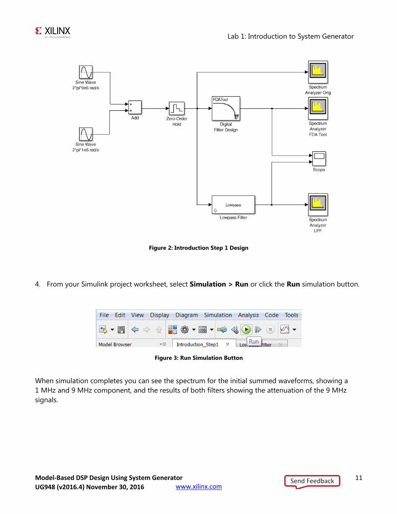
3. Open the Lab1_1 design as follows:
At the MATLAB command prompt, type open Lab1_1.slx
OR
Double-click Lab1_1.slx in the Current Folder browser.
The Lab1_1 design opens, showing two sine wave sources being added together and passed separately
through two low-pass filters. This design highlights that a low-pass filter may be implemented using the
Simulink FDATool or Lowpass Filter blocks.
Send FeedbackUG948 (v2016.4) November 30, 2016
Lab 1: Introduction to System Generator
Model-Based DSP Design Using System Generator 11 UG948 (v2016.3) October 28, 2016 www.xilinx.com
Figure 2: Introduction Step 1 Design
4. From your Simulink project worksheet, select Simulation > Run or click the Run simulation button.
Figure 3: Run Simulation Button
When simulation completes you can see the spectrum for the initial summed waveforms, showing a
1 MHz and 9 MHz component, and the results of both filters showing the attenuation of the 9 MHz
signals.
Send FeedbackUG948 (v2016.4) November 30, 2016
Lab 1: Introduction to System Generator
Model-Based DSP Design Using System Generator 12 UG948 (v2016.3) October 28, 2016 www.xilinx.com
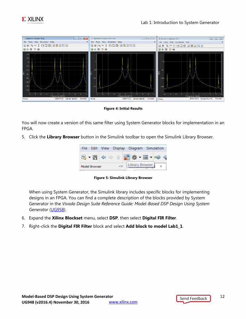
Figure 4: Initial Results
You will now create a version of this same filter using System Generator blocks for implementation in an
FPGA.
5. Click the Library Browser button in the Simulink toolbar to open the Simulink Library Browser.
Figure 5: Simulink Library Browser
When using System Generator, the Simulink library includes specific blocks for implementing
designs in an FPGA. You can find a complete description of the blocks provided by System
Generator in the Vivado Design Suite Reference Guide: Model-Based DSP Design Using System
Generator (UG958).
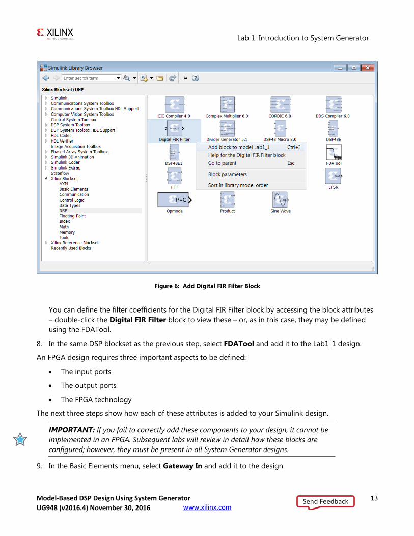
6. Expand the Xilinx Blockset menu, select DSP, then select Digital FIR Filter.
7. Right-click the Digital FIR Filter block and select Add block to model Lab1_1.
Send FeedbackUG948 (v2016.4) November 30, 2016
Lab 1: Introduction to System Generator
Model-Based DSP Design Using System Generator 13 UG948 (v2016.3) October 28, 2016 www.xilinx.com
Figure 6: Add Digital FIR Filter Block
You can define the filter coefficients for the Digital FIR Filter block by accessing the block attributes
– double-click the Digital FIR Filter block to view these – or, as in this case, they may be defined
using the FDATool.
8. In the same DSP blockset as the previous step, select FDATool and add it to the Lab1_1 design.
An FPGA design requires three important aspects to be defined:
The input ports
The output ports
The FPGA technology
The next three steps show how each of these attributes is added to your Simulink design.
IMPORTANT: If you fail to correctly add these components to your design, it cannot be
implemented in an FPGA. Subsequent labs will review in detail how these blocks are
configured; however, they must be present in all System Generator designs.
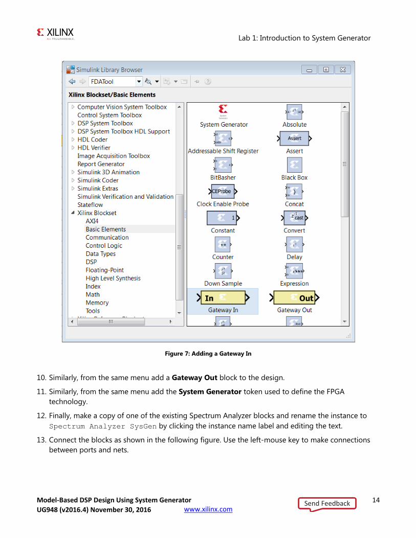
9. In the Basic Elements menu, select Gateway In and add it to the design.
Send FeedbackUG948 (v2016.4) November 30, 2016
Lab 1: Introduction to System Generator
Model-Based DSP Design Using System Generator 14 UG948 (v2016.3) October 28, 2016 www.xilinx.com
Figure 7: Adding a Gateway In
10. Similarly, from the same menu add a Gateway Out block to the design.
11. Similarly, from the same menu add the System Generator token used to define the FPGA
technology.
12. Finally, make a copy of one of the existing Spectrum Analyzer blocks and rename the instance to
Spectrum Analyzer SysGen by clicking the instance name label and editing the text.
13. Connect the blocks as shown in the following figure. Use the left-mouse key to make connections
between ports and nets.
Send FeedbackUG948 (v2016.4) November 30, 2016

Lab 1: Introduction to System Generator
Model-Based DSP Design Using System Generator 15 UG948 (v2016.3) October 28, 2016 www.xilinx.com
Figure 8: Initial System Generator Design
The next part of the design process is to configure the System Generator blocks.
Configure the System Generator Blocks
The first task is to define the coefficients of the new filter. For this task you will use the Xilinx block
version of FDATool. If you open the existing FDATool block, you can review the existing Frequency and
Magnitude specifications.
1. Double-click the Digital Filter Design instance to open the Properties Editor.
This allows you to review the properties of the existing filter.
Send FeedbackUG948 (v2016.4) November 30, 2016

Lab 1: Introduction to System Generator
Model-Based DSP Design Using System Generator 16 UG948 (v2016.3) October 28, 2016 www.xilinx.com
Figure 9: Filter Specifications
2. Close the Properties Editor for the Digital Filter Design instance.
3. Double-click the FDATool instance to open the Properties Editor.
4. Adjust the filter specifications to the following values (shown in the figure above):
Frequency Specifications
o Units = MHz
o Fs = 20
o Fpass = 1.5
o Fstop = 8.5
Send FeedbackUG948 (v2016.4) November 30, 2016
Lab 1: Introduction to System Generator
Model-Based DSP Design Using System Generator 17 UG948 (v2016.3) October 28, 2016 www.xilinx.com
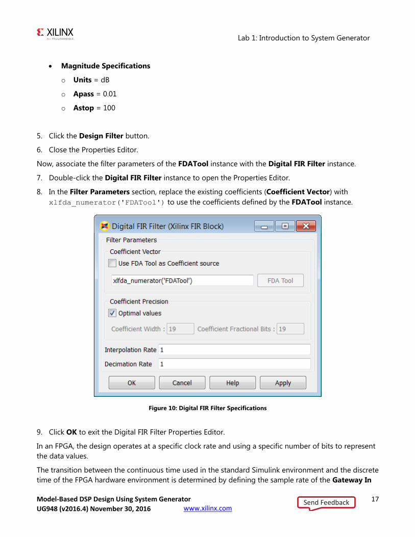
Magnitude Specifications
o Units = dB
o Apass = 0.01
o Astop = 100
5. Click the Design Filter button.
6. Close the Properties Editor.
Now, associate the filter parameters of the FDATool instance with the Digital FIR Filter instance.
7. Double-click the Digital FIR Filter instance to open the Properties Editor.
8. In the Filter Parameters section, replace the existing coefficients (Coefficient Vector) with
xlfda_numerator('FDATool') to use the coefficients defined by the FDATool instance.
Figure 10: Digital FIR Filter Specifications
9. Click OK to exit the Digital FIR Filter Properties Editor.
In an FPGA, the design operates at a specific clock rate and using a specific number of bits to represent
the data values.
The transition between the continuous time used in the standard Simulink environment and the discrete
time of the FPGA hardware environment is determined by defining the sample rate of the Gateway In
Send FeedbackUG948 (v2016.4) November 30, 2016

Lab 1: Introduction to System Generator
Model-Based DSP Design Using System Generator 18 UG948 (v2016.3) October 28, 2016 www.xilinx.com
blocks. This determines how often the continuous input waveform is sampled. This sample rate is
automatically propagated to other blocks in the design by System Generator. In a similar manner, the
number of bits used to represent the data is defined in the Gateway In block and also propagated
through the system.
Although not used in this tutorial, some Xilinx blocks enable rate changes and bit-width changes, up or
down, as part of this automatic propagation. More details on these blocks are found in the Vivado
Design Suite Reference Guide: Model-Based DSP Design Using System Generator (UG958).
Both of these attributes (rate and bit width) determine the degree of accuracy with which the
continuous time signal is represented. Both of these attributes also have an impact on the size,
performance, and hence cost of the final hardware.
System Generator allows you to use the Simulink environment to define, simulate, and review the
impact of these attributes.
10. Double-click the Gateway In block to open the Properties Editor.
Because the highest frequency sine wave in the design is 9 MHz, sampling theory dictates the sampling
frequency of the input port must be at least 18 MHz. For this design, you will use 20 MHz.
11. At the bottom of the Properties Editor, set the Sample Period to 1/20e6.
12. For now, leave the bit width as the default fixed-point 2’s complement 16-bits with 14-bits
representing the data below the binary point. This allows us to express a range of -2.0 to 1.999,
which exceeds the range required for the summation of the sine waves (both of amplitude 1).
Send FeedbackUG948 (v2016.4) November 30, 2016

Lab 1: Introduction to System Generator
Model-Based DSP Design Using System Generator 19 UG948 (v2016.3) October 28, 2016 www.xilinx.com
Figure 11: Gateway In Properties
13. Click OK to close the Gateway In Properties Editor.
This now allows us to use accurate sample rate and bit-widths to accurately verify the hardware.
14. Double-click the System Generator token to open the Properties Editor.
Because the input port is sampled at 20 MHz to adequately represent the data, you must define the
clock rate of the FPGA and the Simulink sample period to be at least 20 MHz.
Send FeedbackUG948 (v2016.4) November 30, 2016
Lab 1: Introduction to System Generator
Model-Based DSP Design Using System Generator 20 UG948 (v2016.3) October 28, 2016 www.xilinx.com
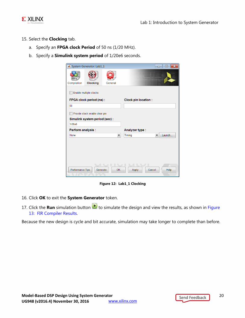
15. Select the Clocking tab.
a. Specify an FPGA clock Period of 50 ns (1/20 MHz).
b. Specify a Simulink system period of 1/20e6 seconds.
Figure 12: Lab1_1 Clocking
16. Click OK to exit the System Generator token.
17. Click the Run simulation button to simulate the design and view the results, as shown in Figure
13: FIR Compiler Results.
Because the new design is cycle and bit accurate, simulation may take longer to complete than before.
Send FeedbackUG948 (v2016.4) November 30, 2016
Lab 1: Introduction to System Generator
Model-Based DSP Design Using System Generator 21 UG948 (v2016.3) October 28, 2016 www.xilinx.com
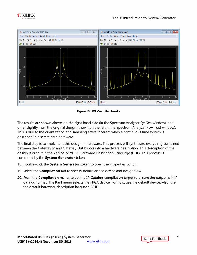
Figure 13: FIR Compiler Results
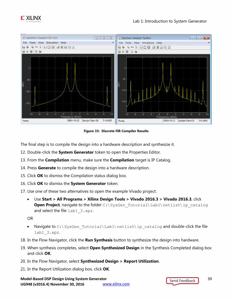
The results are shown above, on the right hand side (in the Spectrum Analyzer SysGen window), and
differ slightly from the original design (shown on the left in the Spectrum Analyzer FDA Tool window).
This is due to the quantization and sampling effect inherent when a continuous time system is
described in discrete time hardware.
The final step is to implement this design in hardware. This process will synthesize everything contained
between the Gateway In and Gateway Out blocks into a hardware description. This description of the
design is output in the Verilog or VHDL Hardware Description Language (HDL). This process is
controlled by the System Generator token.
18. Double-click the System Generator token to open the Properties Editor.
19. Select the Compilation tab to specify details on the device and design flow.
20. From the Compilation menu, select the IP Catalog compilation target to ensure the output is in IP
Catalog format. The Part menu selects the FPGA device. For now, use the default device. Also, use
the default hardware description language, VHDL.
Send FeedbackUG948 (v2016.4) November 30, 2016

Lab 1: Introduction to System Generator
Model-Based DSP Design Using System Generator 22 UG948 (v2016.3) October 28, 2016 www.xilinx.com
Figure 14: System Generator Token for Lab 1 Step 1
21. Click Generate to compile the design into hardware.
The compilation process transforms the design captured in Simulink blocks into an industry
standard RTL (Register Transfer Level) design description. The RTL design can be synthesized into a
hardware design. The Compilation status dialog box appears when the hardware design description
has been generated.
Figure 15: Generation Complete
22. Click OK to dismiss the Compilation status dialog box.
23. Click OK to dismiss the System Generator token.
The final step in the design process is to create the hardware and review the results.
Send FeedbackUG948 (v2016.4) November 30, 2016

Lab 1: Introduction to System Generator
Model-Based DSP Design Using System Generator 23 UG948 (v2016.3) October 28, 2016 www.xilinx.com
Create the Hardware and Review the Results
The output from design compilation process is written to the netlist directory. This directory
contains three subdirectories:
sysgen: This contains the RTL design description written in the industry standard VHDL format.
This is provided for users experienced in hardware design who wish to view the detailed results.
ip: This directory contains the design IP, captured in Xilinx IP Catalog format, which is used to
transfer the design into the Xilinx Vivado Design Suite. Lab 8: Using AXI Interfaces and IP
Integrator, presented later in this document, explains in detail how to transfer your design IP
into the Vivado Design Suite for implementation in an FPGA.
ip_catalog: This directory contains an example Vivado project with the design IP already
included. This project is provided only as a means of quick analysis.
You will now review the results in hardware by using the example Vivado project in the ip_catalog
directory.
IMPORTANT: The Vivado project provided in the ip_catalog directory does not
contain top-level I/O buffers. The results of synthesis provide a very good estimate of
the final design results; however, the results from this project cannot be used to create
the final FPGA.
24. Invoke the Vivado Design Suite: Start > All Programs > Xilinx Design Tools > Vivado 2016.3 >
Vivado 2016.3.
25. Click Open Project and then navigate to the folder
C:\SysGen_Tutorial\Lab1\netlist\ip_catalog.
26. Select file lab1_1.xpr and the Vivado IDE invokes the generated project file.
27. Click the Run Synthesis button to synthesize the design into hardware.
Send FeedbackUG948 (v2016.4) November 30, 2016

Lab 1: Introduction to System Generator
Model-Based DSP Design Using System Generator 24 UG948 (v2016.3) October 28, 2016 www.xilinx.com
Figure 16: Vivado Project for Design Lab1_1
Send FeedbackUG948 (v2016.4) November 30, 2016
Lab 1: Introduction to System Generator
Model-Based DSP Design Using System Generator 25 UG948 (v2016.3) October 28, 2016 www.xilinx.com
To get an exact confirmation of the final resources and timing, you could select Run Implementation
when the synthesis finishes. However, the results after synthesis provide a very good approximation of
the final results without the additional run time of implementing a fully placed and routed design and is
recommended early in the design cycle.
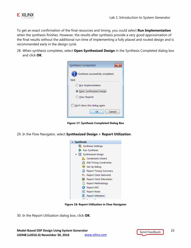
28. When synthesis completes, select Open Synthesized Design in the Synthesis Completed dialog box
and click OK.
Figure 17: Synthesis Completed Dialog Box
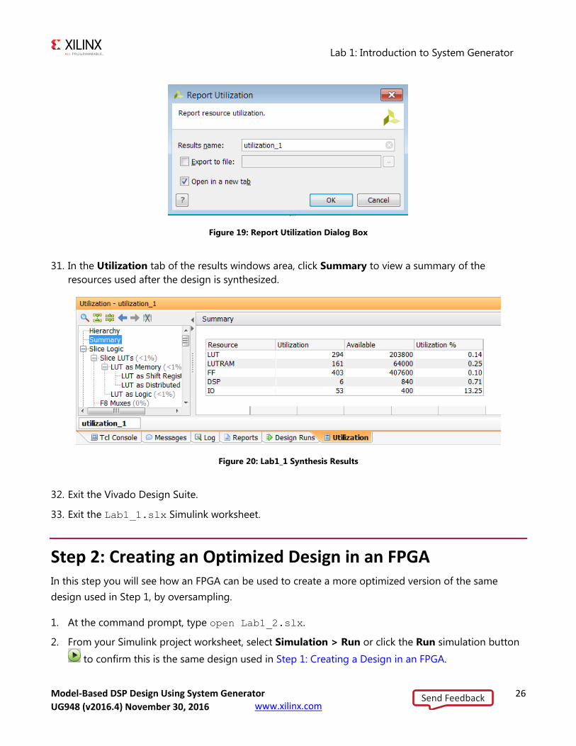
29. In the Flow Navigator, select Synthesized Design > Report Utilization.
Figure 18: Report Utilization in Flow Navigator
30. In the Report Utilization dialog box, click OK.
Send FeedbackUG948 (v2016.4) November 30, 2016
Lab 1: Introduction to System Generator
Model-Based DSP Design Using System Generator 26 UG948 (v2016.3) October 28, 2016 www.xilinx.com
Figure 19: Report Utilization Dialog Box
31. In the Utilization tab of the results windows area, click Summary to view a summary of the
resources used after the design is synthesized.
Figure 20: Lab1_1 Synthesis Results
32. Exit the Vivado Design Suite.
33. Exit the Lab1_1.slx Simulink worksheet.
Step 2: Creating an Optimized Design in an FPGA In this step you will see how an FPGA can be used to create a more optimized version of the same
design used in Step 1, by oversampling.
1. At the command prompt, type open Lab1_2.slx.
2. From your Simulink project worksheet, select Simulation > Run or click the Run simulation button
to confirm this is the same design used in Step 1: Creating a Design in an FPGA.
Send FeedbackUG948 (v2016.4) November 30, 2016
Lab 1: Introduction to System Generator
Model-Based DSP Design Using System Generator 27 UG948 (v2016.3) October 28, 2016 www.xilinx.com
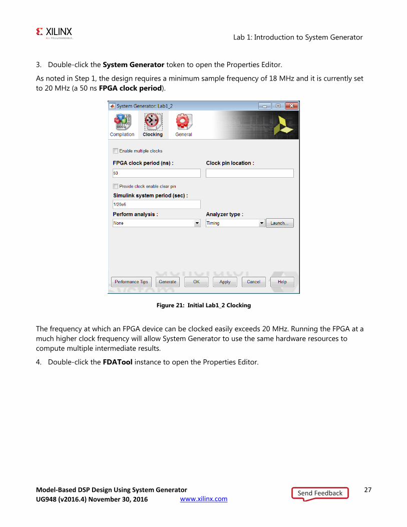
3. Double-click the System Generator token to open the Properties Editor.
As noted in Step 1, the design requires a minimum sample frequency of 18 MHz and it is currently set
to 20 MHz (a 50 ns FPGA clock period).
Figure 21: Initial Lab1_2 Clocking
The frequency at which an FPGA device can be clocked easily exceeds 20 MHz. Running the FPGA at a
much higher clock frequency will allow System Generator to use the same hardware resources to
compute multiple intermediate results.
4. Double-click the FDATool instance to open the Properties Editor.
Send FeedbackUG948 (v2016.4) November 30, 2016
Lab 1: Introduction to System Generator
Model-Based DSP Design Using System Generator 28 UG948 (v2016.3) October 28, 2016 www.xilinx.com
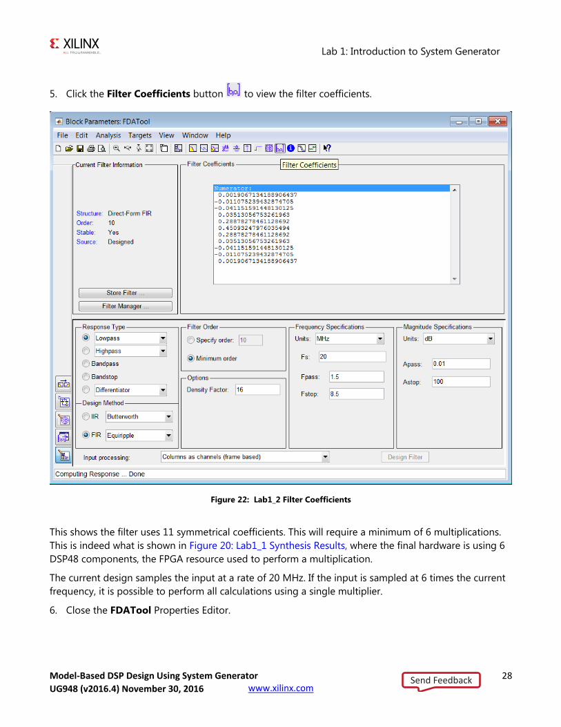
5. Click the Filter Coefficients button to view the filter coefficients.
Figure 22: Lab1_2 Filter Coefficients
This shows the filter uses 11 symmetrical coefficients. This will require a minimum of 6 multiplications.
This is indeed what is shown in Figure 20: Lab1_1 Synthesis Results, where the final hardware is using 6
DSP48 components, the FPGA resource used to perform a multiplication.
The current design samples the input at a rate of 20 MHz. If the input is sampled at 6 times the current
frequency, it is possible to perform all calculations using a single multiplier.
6. Close the FDATool Properties Editor.
Send FeedbackUG948 (v2016.4) November 30, 2016
Lab 1: Introduction to System Generator
Model-Based DSP Design Using System Generator 29 UG948 (v2016.3) October 28, 2016 www.xilinx.com
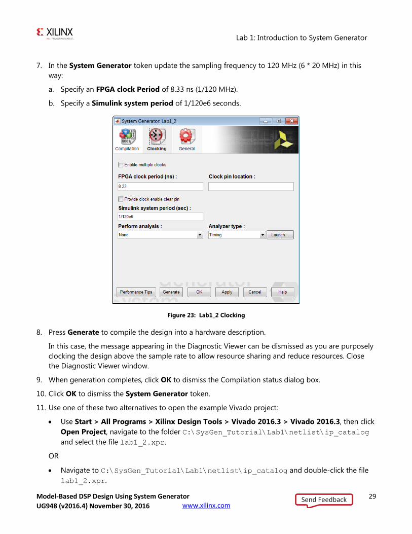
7. In the System Generator token update the sampling frequency to 120 MHz (6 * 20 MHz) in this
way:
a. Specify an FPGA clock Period of 8.33 ns (1/120 MHz).
b. Specify a Simulink system period of 1/120e6 seconds.
Figure 23: Lab1_2 Clocking
8. Press Generate to compile the design into a hardware description.
In this case, the message appearing in the Diagnostic Viewer can be dismissed as you are purposely
clocking the design above the sample rate to allow resource sharing and reduce resources. Close
the Diagnostic Viewer window.
9. When generation completes, click OK to dismiss the Compilation status dialog box.
10. Click OK to dismiss the System Generator token.
11. Use one of these two alternatives to open the example Vivado project:
Use Start > All Programs > Xilinx Design Tools > Vivado 2016.3 > Vivado 2016.3, then click
Open Project, navigate to the folder C:\SysGen_Tutorial\Lab1\netlist\ip_catalog
and select the file lab1_2.xpr.
OR
Navigate to C:\SysGen_Tutorial\Lab1\netlist\ip_catalog and double-click the file
lab1_2.xpr.
Send FeedbackUG948 (v2016.4) November 30, 2016
Lab 1: Introduction to System Generator
Model-Based DSP Design Using System Generator 30 UG948 (v2016.3) October 28, 2016 www.xilinx.com
12. In the Flow Navigator, click the Run Synthesis button to synthesize the design into hardware.
13. When synthesis completes, select Open Synthesized Design in the Synthesis Completed dialog box
and click OK.
14. In the Flow Navigator, select Synthesized Design > Report Utilization.
15. In the Report Utilization dialog box, click OK.
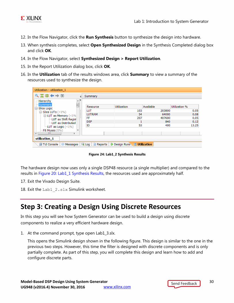
16. In the Utilization tab of the results windows area, click Summary to view a summary of the
resources used to synthesize the design.
Figure 24: Lab1_2 Synthesis Results
The hardware design now uses only a single DSP48 resource (a single multiplier) and compared to the
results in Figure 20: Lab1_1 Synthesis Results, the resources used are approximately half.
17. Exit the Vivado Design Suite.
18. Exit the Lab1_2.slx Simulink worksheet.
Step 3: Creating a Design Using Discrete Resources In this step you will see how System Generator can be used to build a design using discrete
components to realize a very efficient hardware design.
1. At the command prompt, type open Lab1_3.slx.
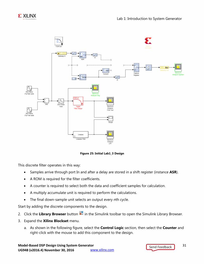
This opens the Simulink design shown in the following figure. This design is similar to the one in the
previous two steps. However, this time the filter is designed with discrete components and is only
partially complete. As part of this step, you will complete this design and learn how to add and
configure discrete parts.
Send FeedbackUG948 (v2016.4) November 30, 2016
Lab 1: Introduction to System Generator
Model-Based DSP Design Using System Generator 31 UG948 (v2016.3) October 28, 2016 www.xilinx.com
Figure 25: Initial Lab1_3 Design
This discrete filter operates in this way:
Samples arrive through port In and after a delay are stored in a shift register (instance ASR).
A ROM is required for the filter coefficients.
A counter is required to select both the data and coefficient samples for calculation.
A multiply accumulate unit is required to perform the calculations.
The final down-sample unit selects an output every nth cycle.
Start by adding the discrete components to the design.
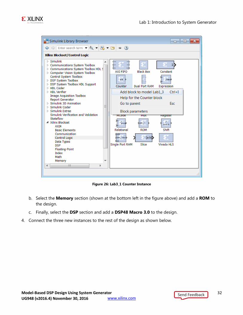
2. Click the Library Browser button in the Simulink toolbar to open the Simulink Library Browser.
3. Expand the Xilinx Blockset menu.
a. As shown in the following figure, select the Control Logic section, then select the Counter and
right-click with the mouse to add this component to the design.
Send FeedbackUG948 (v2016.4) November 30, 2016
Lab 1: Introduction to System Generator
Model-Based DSP Design Using System Generator 32 UG948 (v2016.3) October 28, 2016 www.xilinx.com
Figure 26: Lab3_1 Counter Instance
b. Select the Memory section (shown at the bottom left in the figure above) and add a ROM to
the design.
c. Finally, select the DSP section and add a DSP48 Macro 3.0 to the design.
4. Connect the three new instances to the rest of the design as shown below.
Send FeedbackUG948 (v2016.4) November 30, 2016
Lab 1: Introduction to System Generator
Model-Based DSP Design Using System Generator 33 UG948 (v2016.3) October 28, 2016 www.xilinx.com
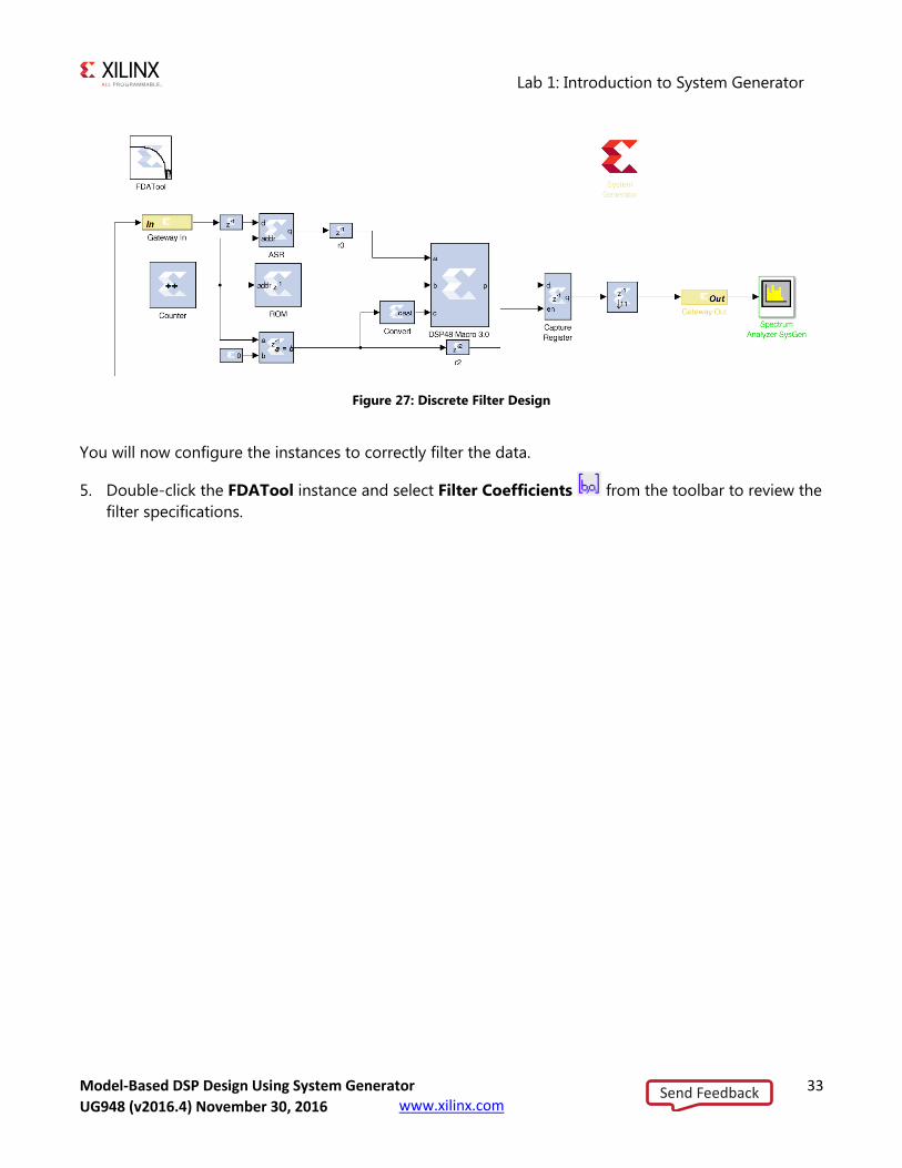
Figure 27: Discrete Filter Design
You will now configure the instances to correctly filter the data.
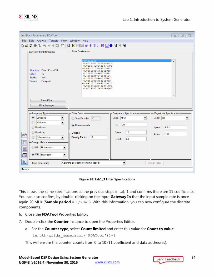
5. Double-click the FDATool instance and select Filter Coefficients from the toolbar to review the
filter specifications.
Send FeedbackUG948 (v2016.4) November 30, 2016
Lab 1: Introduction to System Generator
Model-Based DSP Design Using System Generator 34 UG948 (v2016.3) October 28, 2016 www.xilinx.com
Figure 28: Lab1_3 Filter Specifications
This shows the same specifications as the previous steps in Lab 1 and confirms there are 11 coefficients.
You can also confirm, by double-clicking on the input Gateway In that the input sample rate is once
again 20 MHz (Sample period = 1/20e6). With this information, you can now configure the discrete
components.
6. Close the FDATool Properties Editor.
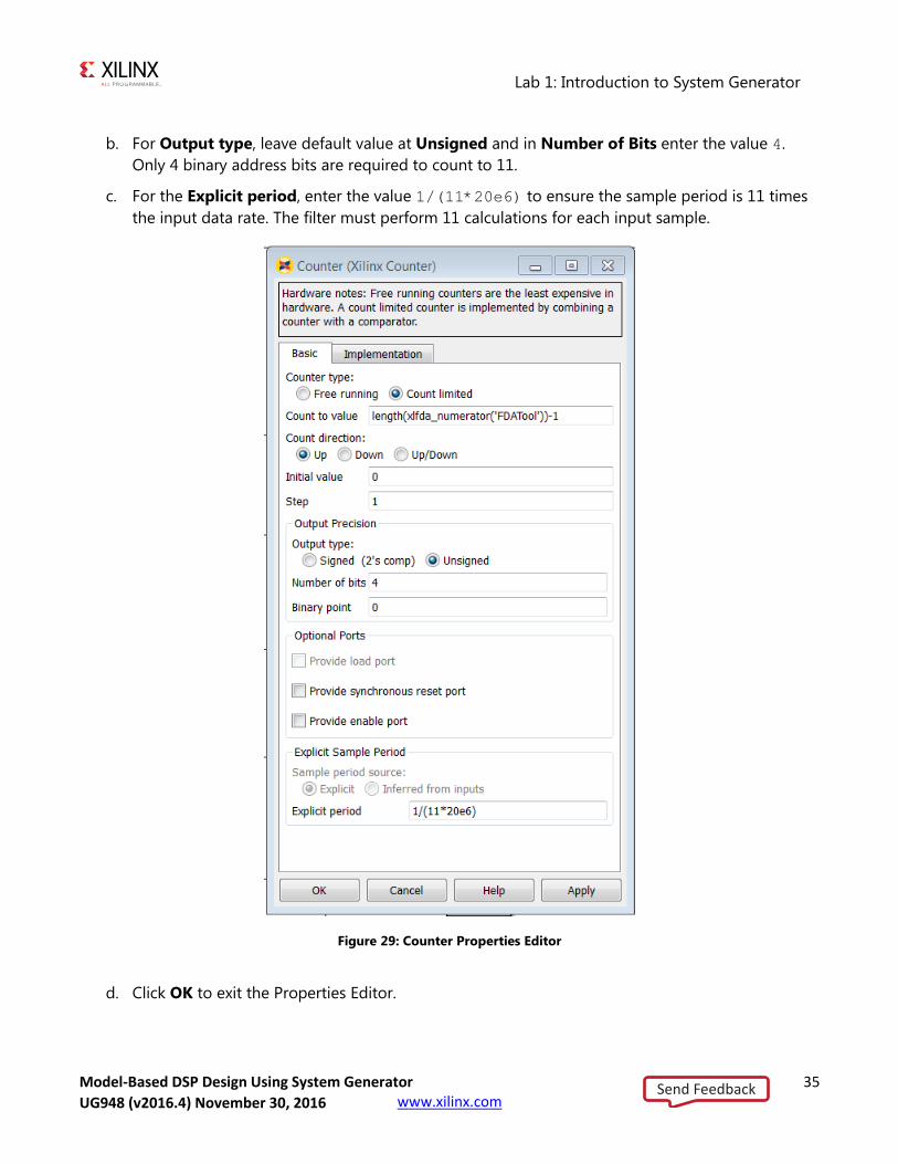
7. Double-click the Counter instance to open the Properties Editor.
a. For the Counter type, select Count limited and enter this value for Count to value:
length(xlfda_numerator('FDATool'))-1
This will ensure the counter counts from 0 to 10 (11 coefficient and data addresses).
Send FeedbackUG948 (v2016.4) November 30, 2016
Lab 1: Introduction to System Generator
Model-Based DSP Design Using System Generator 35 UG948 (v2016.3) October 28, 2016 www.xilinx.com
b. For Output type, leave default value at Unsigned and in Number of Bits enter the value 4.
Only 4 binary address bits are required to count to 11.
c. For the Explicit period, enter the value 1/(11*20e6) to ensure the sample period is 11 times
the input data rate. The filter must perform 11 calculations for each input sample.
Figure 29: Counter Properties Editor
d. Click OK to exit the Properties Editor.
Send FeedbackUG948 (v2016.4) November 30, 2016
Lab 1: Introduction to System Generator
Model-Based DSP Design Using System Generator 36 UG948 (v2016.3) October 28, 2016 www.xilinx.com
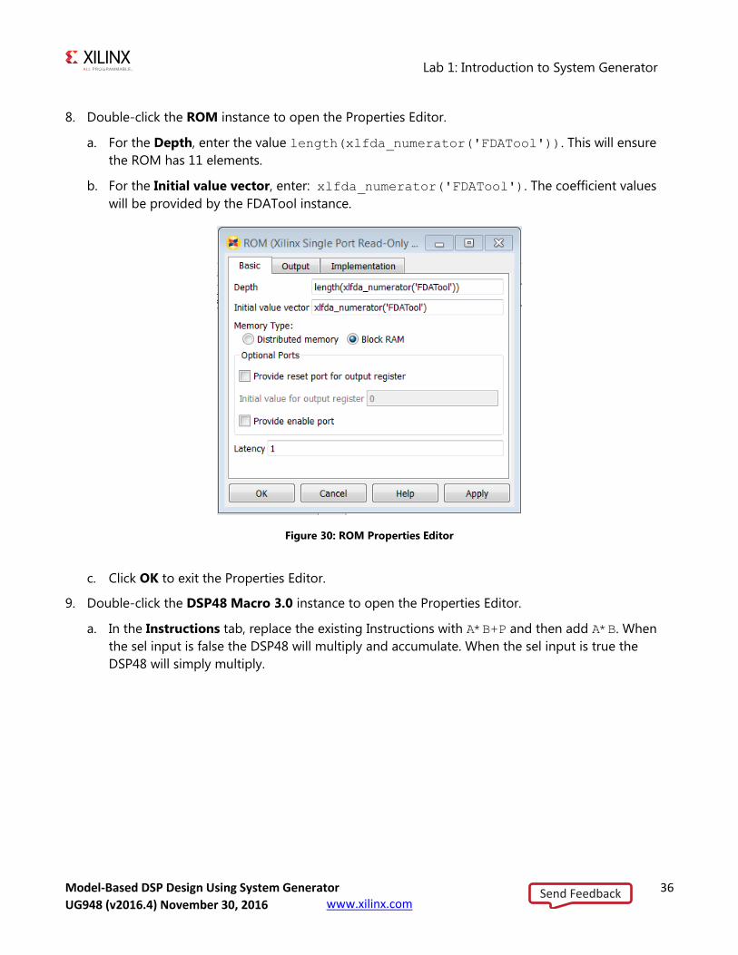
8. Double-click the ROM instance to open the Properties Editor.
a. For the Depth, enter the value length(xlfda_numerator('FDATool')). This will ensure
the ROM has 11 elements.
b. For the Initial value vector, enter: xlfda_numerator('FDATool'). The coefficient values
will be provided by the FDATool instance.
Figure 30: ROM Properties Editor
c. Click OK to exit the Properties Editor.
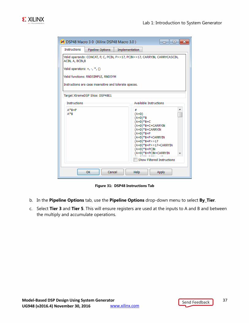
9. Double-click the DSP48 Macro 3.0 instance to open the Properties Editor.
a. In the Instructions tab, replace the existing Instructions with A*B+P and then add A*B. When
the sel input is false the DSP48 will multiply and accumulate. When the sel input is true the
DSP48 will simply multiply.
Send FeedbackUG948 (v2016.4) November 30, 2016
Lab 1: Introduction to System Generator
Model-Based DSP Design Using System Generator 37 UG948 (v2016.3) October 28, 2016 www.xilinx.com
Figure 31: DSP48 Instructions Tab
b. In the Pipeline Options tab, use the Pipeline Options drop-down menu to select By_Tier.
c. Select Tier 3 and Tier 5. This will ensure registers are used at the inputs to A and B and between
the multiply and accumulate operations.
Send FeedbackUG948 (v2016.4) November 30, 2016

Lab 1: Introduction to System Generator
Model-Based DSP Design Using System Generator 38 UG948 (v2016.3) October 28, 2016 www.xilinx.com
Figure 32: DSP48 Pipeline Options Tab
d. Click OK to exit the Properties Editor.
10. Use the Save to save the design.
11. Click the Run simulation button to simulate the design and view the results, as shown in the figure
below.
Send FeedbackUG948 (v2016.4) November 30, 2016
Lab 1: Introduction to System Generator
Model-Based DSP Design Using System Generator 39 UG948 (v2016.3) October 28, 2016 www.xilinx.com
Figure 33: Discrete FIR Compiler Results
The final step is to compile the design into a hardware description and synthesize it.
12. Double-click the System Generator token to open the Properties Editor.
13. From the Compilation menu, make sure the Compilation target is IP Catalog.
14. Press Generate to compile the design into a hardware description.
15. Click OK to dismiss the Compilation status dialog box.
16. Click OK to dismiss the System Generator token.
17. Use one of these two alternatives to open the example Vivado project:
Use Start > All Programs > Xilinx Design Tools > Vivado 2016.3 > Vivado 2016.3, click
Open Project, navigate to the folder C:\SysGen_Tutorial\Lab1\netlist\ip_catalog
and select the file lab1_3.xpr.
OR
Navigate to C:\SysGen_Tutorial\Lab1\netlist\ip_catalog and double-click the file
lab1_3.xpr.
18. In the Flow Navigator, click the Run Synthesis button to synthesize the design into hardware.
19. When synthesis completes, select Open Synthesized Design in the Synthesis Completed dialog box
and click OK.
20. In the Flow Navigator, select Synthesized Design > Report Utilization.
21. In the Report Utilization dialog box, click OK.
Send FeedbackUG948 (v2016.4) November 30, 2016

Lab 1: Introduction to System Generator
Model-Based DSP Design Using System Generator 40 UG948 (v2016.3) October 28, 2016 www.xilinx.com
22. In the Utilization tab of the results windows area, click Summary to view a summary of the
resources used to synthesize the design.
Figure 34: Lab1_3 Synthesis Results
The design now uses fewer FPGA hardware resources than either of the versions designed with the
Digital FIR Filter macro (Figure 20: Lab1_1 Synthesis Results and Figure 24: Lab1_2 Synthesis Results).
23. Exit the Vivado Design Suite.
24. Exit the Lab1_3.slx worksheet.
Summary In this lab, you learned how to use the System Generator blockset to create a design in the Simulink
environment and synthesize the design in hardware which can be implemented on a Xilinx FPGA. You
learned the benefits of quickly creating your design using a Xilinx Digital FIR Filter block and how the
design could be improved with the use of over-sampling.
Finally, you learned how you can take total control of the hardware implementation by using discrete
primitives.
Note: In this tutorial you learned how to add System Generator blocks to the design and then
configure them. A useful productivity technique is to add and configure the System Generator
token first. If the target device is set at the start, some complex IP blocks will be automatically
configured for the device when they are added to the design.
The following solutions directory contains the final System Generator (*.slx) files for this lab. The
solutions directory does not contain the IP output from System Generator or the files and directories
generated when Vivado is executed.
C:/SysGen_Tutorial/Lab1/solution
Send FeedbackUG948 (v2016.4) November 30, 2016
Model-Based DSP Design Using System Generator 41 UG948 (v2016.3) October 28, 2016 www.xilinx.com
Lab 2: Working with Data Types
Introduction In this lab exercise, you will learn how hardware-efficient fixed-point types can be used to create a
design which meets the required specification but is more efficient in resources, and understand how to
use Xilinx Blocksets to analyze these systems.
Objectives
After completing this lab, you will be able to:
Understand the hardware implementation cost of a standard Simulink design.
Implement the design using efficient Fixed-Point data types.
Understand how to manipulate data types to ensure an optimal implementation of the design.
Procedure
This exercise has two primary parts.
In Step 1 you will review and synthesize a design using floating-point data types.
In Step 2 you will work with the same design, captured as a fixed-point implementation, and
refine the data types to create a hardware-efficient design which meets the same requirements.
Send FeedbackUG948 (v2016.4) November 30, 2016
Lab 2: Working with Data Types
Model-Based DSP Design Using System Generator 42 UG948 (v2016.3) October 28, 2016 www.xilinx.com
Step 1: Designing with Floating-Point Data Types In this step you will review a design implemented with floating-point data types.
1. Invoke System Generator.
On Windows systems select Start > All Programs > Xilinx Design Tools > Vivado 2016.3 >
System Generator > System Generator 2016.3.
On Linux systems, type sysgen at the command prompt.
2. Navigate to the Lab2 folder: cd C:\SysGen_Tutorial\Lab2.
You can view the directory contents in the MATLAB Current Directory window, or type ls at the
command line prompt.
3. At the command prompt, type open Lab2_1.slx
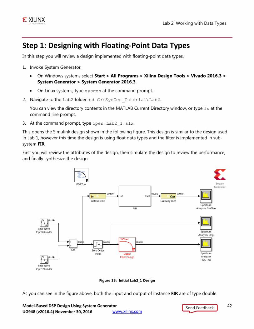
This opens the Simulink design shown in the following figure. This design is similar to the design used
in Lab 1, however this time the design is using float data types and the filter is implemented in sub-
system FIR.
First you will review the attributes of the design, then simulate the design to review the performance,
and finally synthesize the design.
Figure 35: Initial Lab2_1 Design
As you can see in the figure above, both the input and output of instance FIR are of type double.
Send FeedbackUG948 (v2016.4) November 30, 2016

Lab 2: Working with Data Types
Model-Based DSP Design Using System Generator 43 UG948 (v2016.3) October 28, 2016 www.xilinx.com
4. In the MATLAB Command Window enter MyCoeffs = xlfda_numerator('FDATool').
5. Double-click the instance FIR to open the sub-system.
6. Double-click the instance Constant1 to open the Properties Editor.
This shows the Constant value is defined by MyCoeffs(1).
Figure 36: Constant1 Properties Editor
7. Close the Constant1 Properties editor.
8. Return to the top-level design using the toolbar button Up To Parent , or click on the tab labeled
Lab2_1.
The design is summing two sine waves, both of which are 9 MHz. The input gateway to the System
Generator must therefore sample at a rate of at least 18 MHz.
9. Double-click the Gateway In1 instance to open the Properties Editor and confirm the input is
sampling the data at a rate of 20 MHz (a Sample period of 1/20e6).
10. Close the Gateway In Properties editor.
11. Press the Run simulation button to simulate the design.
Send FeedbackUG948 (v2016.4) November 30, 2016
Lab 2: Working with Data Types
Model-Based DSP Design Using System Generator 44 UG948 (v2016.3) October 28, 2016 www.xilinx.com
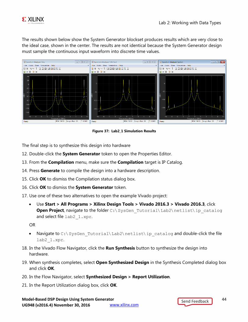
The results shown below show the System Generator blockset produces results which are very close to
the ideal case, shown in the center. The results are not identical because the System Generator design
must sample the continuous input waveform into discrete time values.
Figure 37: Lab2_1 Simulation Results
The final step is to synthesize this design into hardware
12. Double-click the System Generator token to open the Properties Editor.
13. From the Compilation menu, make sure the Compilation target is IP Catalog.
14. Press Generate to compile the design into a hardware description.
15. Click OK to dismiss the Compilation status dialog box.
16. Click OK to dismiss the System Generator token.
17. Use one of these two alternatives to open the example Vivado project:
Use Start > All Programs > Xilinx Design Tools > Vivado 2016.3 > Vivado 2016.3, click
Open Project, navigate to the folder C:\SysGen_Tutorial\Lab2\netlist\ip_catalog
and select file lab2_1.xpr.
OR
Navigate to C:\SysGen_Tutorial\Lab2\netlist\ip_catalog and double-click the file
lab2_1.xpr.
18. In the Vivado Flow Navigator, click the Run Synthesis button to synthesize the design into
hardware.
19. When synthesis completes, select Open Synthesized Design in the Synthesis Completed dialog box
and click OK.
20. In the Flow Navigator, select Synthesized Design > Report Utilization.
21. In the Report Utilization dialog box, click OK.
Send FeedbackUG948 (v2016.4) November 30, 2016
Lab 2: Working with Data Types
Model-Based DSP Design Using System Generator 45 UG948 (v2016.3) October 28, 2016 www.xilinx.com
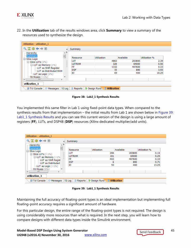
22. In the Utilization tab of the results windows area, click Summary to view a summary of the
resources used to synthesize the design.
Figure 38: Lab2_1 Synthesis Results
You implemented this same filter in Lab 1 using fixed-point data types. When compared to the
synthesis results from that implementation – the initial results from Lab 1 are shown below in Figure 39:
Lab1_1 Synthesis Results and you can see this current version of the design is using a large amount of
registers (FF), LUTs, and DSP48 (DSP) resources (Xilinx dedicated multiplier/add units).
Figure 39: Lab1_1 Synthesis Results
Maintaining the full accuracy of floating-point types is an ideal implementation but implementing full
floating-point accuracy requires a significant amount of hardware.
For this particular design, the entire range of the floating-point types is not required. The design is
using considerably more resources than what is required. In the next step, you will learn how to
compare designs with different data types inside the Simulink environment.
Send FeedbackUG948 (v2016.4) November 30, 2016
Lab 2: Working with Data Types
Model-Based DSP Design Using System Generator 46 UG948 (v2016.3) October 28, 2016 www.xilinx.com
23. Exit the Vivado Design Suite.
24. Exit the Lab2_1.slx Simulink worksheet.
Step 2: Designing with Fixed-Point Data Types In this step you will re-implement the design from Step 1: Designing with Floating-Point Data Types
using fixed-point data types, and compare this new design with the original design. This exercise will
demonstrate the advantages and disadvantages of using fixed-point types and how System Generator
allows you to easily compare the designs, allowing you to make trade-offs between accuracy and
resources within the Simulink environment before committing to an FPGA implementation.
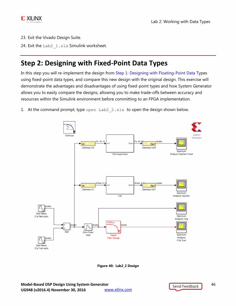
1. At the command prompt, type open Lab2_2.slx to open the design shown below.
Figure 40: Lab2_2 Design
Send FeedbackUG948 (v2016.4) November 30, 2016

Lab 2: Working with Data Types
Model-Based DSP Design Using System Generator 47 UG948 (v2016.3) October 28, 2016 www.xilinx.com
In this design, the floating-point implementation is captured alongside an identical fixed point design.
2. In the MATLAB Command Window enter MyCoeffs = xlfda_numerator('FDATool').
3. Double-click the instance Gateway In2 to confirm the data is being sampled as 16-bit fixed-point
value.
4. Click Cancel to exit the Properties Editor.
5. Click the Run simulation button to simulate the design and confirm instance Spectrum Analyzer
SysGen Fixed shows the filtered output.
As you will see if you examine the output of instance FIR-Fixed-Point (shown in Figure 40: Lab2_2
Design) System Generator has automatically propagated the input data type through the filter and
determined the output must be 43-bit (with 28 binary bits) to maintain the resolution of the signal.
This is based on the bit-growth through the filter and the fact that the filter coefficients (constants in
instance FIR-Fixed-Point) are 16-bit.
6. In the MATLAB Command Window, enter sum(abs(MyCoeffs)) to determine the absolute
maximum gain using the current coefficients.
Figure 41: Lab2_2 Coefficient Sum
Taking into account the positive and negative values of the coefficients the maximum gain possible is
1.2070 and the output signal should only ever be slightly smaller in magnitude than the input signal,
which is a 16-bit signal. There is no need to have 15 bits (43-28) of data above the binary point.
You will now use the Reinterpret and Convert blocks to manipulate the fixed-point data to be no
greater than the width required for an accurate result and produce the most hardware efficient design.
Send FeedbackUG948 (v2016.4) November 30, 2016

Lab 2: Working with Data Types
Model-Based DSP Design Using System Generator 48 UG948 (v2016.3) October 28, 2016 www.xilinx.com
7. Right-click with the mouse anywhere in the canvas and select Xilinx BlockAdd.
8. In the Add Block entry box, type Reinterpret.
9. Double-click the Reinterpret component to add it to the design.
10. Repeat the previous three steps for these components:
a. Convert
b. Scope
11. In the design, select the Gateway Out2 instance.
a. Right-click and use Copy and Paste to create a new instance of the Gateway Out block.
b. Paste twice again to create two more instances of the Gateway Out (for a total of three new
instances).
12. Double-click the Scope component.
a. In the Scope properties dialog box, select File > Number of Inputs > 3.
b. Select View > Configuration Properties and confirm that the Number of input ports is 3.
Figure 42: Configuration Properties Dialog Box
c. Click OK to close the Configuration Properties dialog box.
d. Select File > Close to close the Scope properties dialog box.
Send FeedbackUG948 (v2016.4) November 30, 2016

Lab 2: Working with Data Types
Model-Based DSP Design Using System Generator 49 UG948 (v2016.3) October 28, 2016 www.xilinx.com
13. Connect the blocks as shown in the figure below.
14. Rename the signal names into the scope as shown in the figure below: Convert, Reinterpret and
Growth.
To rename a signal, click the existing name label and edit the text, or if there is no text double-click
the wire and type the name.
Figure 43: Updated Lab2_2 Design
15. Click the Run simulation button to simulate the design.
16. Double-click the Scope to examine the signals.
TIP: You may need to zoom in and adjust the scale in View > Configuration
Properties to view the signals in detail.
Send FeedbackUG948 (v2016.4) November 30, 2016

Lab 2: Working with Data Types
Model-Based DSP Design Using System Generator 50 UG948 (v2016.3) October 28, 2016 www.xilinx.com
Figure 44: Updated Lab2_2 Design Scope
The Reinterpret and Convert blocks have not been configured at this point and so all three signals are
identical.
The Xilinx Reinterpret block forces its output to a new type without any regard for retaining the
numerical value represented by the input. The block allows for unsigned data to be reinterpreted as
signed data, or, conversely, for signed data to be reinterpreted as unsigned. It also allows for the
reinterpretation of the data's scaling, through the repositioning of the binary point within the data.
In this exercise you will scale the data by a factor of 2 to model the presence of additional design
processing which may occur in a larger system. The Reinterpret block may also be used to scale down.
17. Double-click the Reinterpret block to open the Properties Editor.
18. Select Force Binary Point.
19. Enter the value 27 in the input field Output Binary Point and click OK.
The Xilinx Convert block converts each input sample to a number of a desired arithmetic type. For
example, a number can be converted to a signed (two's complement) or unsigned value. It also allows
the signal quantization to be truncated or rounded and the signal overflow to be wrapped, saturated, or
to be flagged as an error.
In this exercise, you will use the Convert block to reduce the size of the 43-bit word back to a 16-bit
value. In this exercise the Reinterpret block has been used to model a more complex design and scaled
Send FeedbackUG948 (v2016.4) November 30, 2016

Lab 2: Working with Data Types
Model-Based DSP Design Using System Generator 51 UG948 (v2016.3) October 28, 2016 www.xilinx.com
the data by a factor of 2. You must therefore ensure the output has enough bits above the binary point
to represent this increase.
20. Double-click the Convert block to open the Properties Editor.
21. In the Fixed-Point Precision section, enter 13 for the Binary Point and click OK.
22. Save the design.
23. Click the Run simulation button to simulate the design.
24. Double-click the Scope to examine the signals.
TIP: You may need to zoom in and adjust the scale in View > Configuration
Properties to view the signals in detail.
In the figure below you can see the output from the filter (Growth) has values between plus and minus
1. The output from the Reinterpret block moves the data values to between plus and minus 2. In this
detailed view of the waveform, the final output (Convert) shows no difference in fidelity, when
compared to the reinterpret results, but uses only 16 bits.
Figure 45: Scaled Lab2_2 Design Scope
The final step is to synthesize this design into hardware.
25. Double-click the System Generator token to open the Properties Editor.
26. From the Compilation menu, make sure the Compilation target is IP Catalog.
Send FeedbackUG948 (v2016.4) November 30, 2016

Lab 2: Working with Data Types
Model-Based DSP Design Using System Generator 52 UG948 (v2016.3) October 28, 2016 www.xilinx.com
27. Click Generate to compile the design into a hardware description.
28. Click OK to dismiss the Compilation status dialog box.
29. Click OK to dismiss the System Generator token.
30. Use one of these two alternatives to open the example Vivado project:
a. Use Start > All Programs > Xilinx Design Tools > Vivado 2016.3 > Vivado 2016.3, click
Open Project, navigate to the folder C:\SysGen_Tutorial\Lab2\netlist\ip_catalog
and select file lab2_2.xpr.
OR
b. Navigate to C:\SysGen_Tutorial\Lab2\netlist\ip_catalog and double-click the file
lab2_2.xpr.
31. In the Vivado Flow Navigator, click the Run Synthesis button to synthesize the design into
hardware.
32. When synthesis completes, select Open Synthesized Design in the Synthesis Completed dialog box
and click OK.
33. In the Flow Navigator, select Synthesized Design > Report Utilization.
34. In the Report Utilization dialog box, click OK.
35. In the Utilization tab of the results windows area, click Summary to view a summary of the
resources used.
Figure 46: Lab2_2 Synthesis Results
Notice, as compared to the results in Step 1 (Figure 38: Lab2_1 Synthesis Results) these results show
approximately
45% more Flip-Flops
20% more LUTs
30% more DSP48s
Send FeedbackUG948 (v2016.4) November 30, 2016
Lab 2: Working with Data Types
Model-Based DSP Design Using System Generator 53 UG948 (v2016.3) October 28, 2016 www.xilinx.com
However, this design contains both the original floating-point filter and the new fixed-point version: the
fixed-point version therefore uses approximately 75-50% fewer resources with the acceptable signal
fidelity and design performance.
36. Exit the Vivado Design Suite.
37. Exit the Lab2_2.slx worksheet.
Summary In this lab, you learned how floating-point types provide a high degree of accuracy but cost many more
resources to implement in an FPGA. You also learned how the System Generator blockset can be used
to both implement a design using more efficient fixed-point data types and compensate for any loss of
accuracy caused by using fixed-point types.
The Reinterpret and Convert blocks are powerful tools which allow you to optimize your design without
needing to perform detailed bit-level optimizations. You can simply use these blocks to convert
between different data types and quickly analyze the results.
The following solutions directory contains the final System Generator (*.slx) files for this lab. The
solutions directory does not contain the IP output from System Generator or the files and directories
generated when Vivado is executed.
C:/SysGen_Tutorial/Lab2/solution
Send FeedbackUG948 (v2016.4) November 30, 2016
Model-Based DSP Design Using System Generator 54 UG948 (v2016.3) October 28, 2016 www.xilinx.com
Lab 3: Working with Multi-Rate Systems
Introduction In this lab exercise, you will learn how to efficiently implement designs with multiple data rates using
multiple clock domains.
Objectives
After completing this lab, you will be able to:
Understand the benefits of using multiple clock domains to implement multi-rate designs.
Understand how to isolate hierarchies using FIFOs to create safe channels for transferring
asynchronous data.
How to implement hierarchies with different clocks.
Procedure
This exercise has three primary parts.
In Step 1, you will learn how to create hierarchies between the clock domains.
In Step 2, you will learn how to add FIFOs between the hierarchies.
In Step 3, you will learn how to add separate clock domains for each hierarchy.
Step 1: Creating Clock Domain Hierarchies In this step you will review a design in which different parts of the design operate at different data rates
and partition the design into subsystems to be implemented in different clock domains.
1. Invoke System Generator.
On Windows systems select Start > All Programs > Xilinx Design Tools > Vivado 2016.3 >
System Generator > System Generator 2016.3.
On Linux Systems, type sysgen at the command prompt.
2. Navigate to the Lab3 folder: cd C:\SysGen_Tutorial\Lab3.
3. At the command prompt, type open Lab3_1.slx
Send FeedbackUG948 (v2016.4) November 30, 2016
Lab 3: Working with Multi-Rate Systems
Model-Based DSP Design Using System Generator 55 UG948 (v2016.3) October 28, 2016 www.xilinx.com
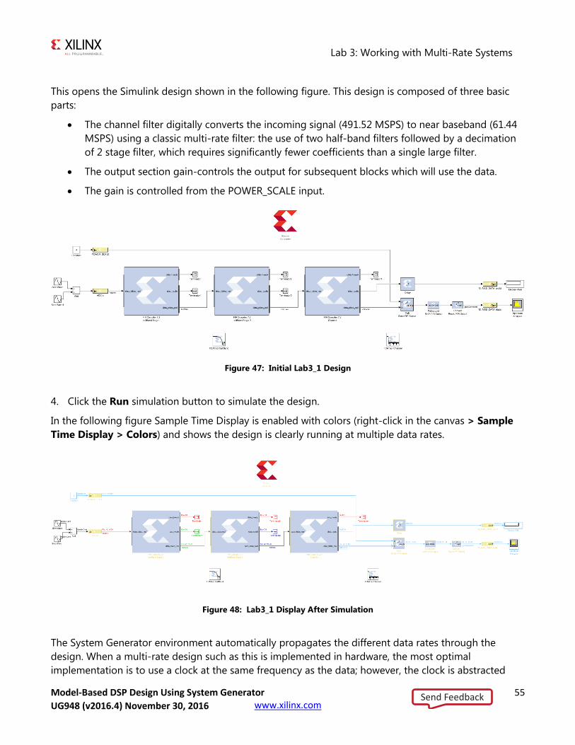
This opens the Simulink design shown in the following figure. This design is composed of three basic
parts:
The channel filter digitally converts the incoming signal (491.52 MSPS) to near baseband (61.44
MSPS) using a classic multi-rate filter: the use of two half-band filters followed by a decimation
of 2 stage filter, which requires significantly fewer coefficients than a single large filter.
The output section gain-controls the output for subsequent blocks which will use the data.
The gain is controlled from the POWER_SCALE input.
Figure 47: Initial Lab3_1 Design
4. Click the Run simulation button to simulate the design.
In the following figure Sample Time Display is enabled with colors (right-click in the canvas > Sample
Time Display > Colors) and shows the design is clearly running at multiple data rates.
Figure 48: Lab3_1 Display After Simulation
The System Generator environment automatically propagates the different data rates through the
design. When a multi-rate design such as this is implemented in hardware, the most optimal
implementation is to use a clock at the same frequency as the data; however, the clock is abstracted
Send FeedbackUG948 (v2016.4) November 30, 2016
Lab 3: Working with Multi-Rate Systems
Model-Based DSP Design Using System Generator 56 UG948 (v2016.3) October 28, 2016 www.xilinx.com
away in this environment. The following methodology demonstrates how to create this ideal
implementation in the most efficient manner.
To efficiently implement a multi-rate (or multi-clock) design using System Generator you should
capture each part running at the same data rate (or clock frequency) in its own hierarchy with its own
System Generator token. The separate hierarchies should then be linked with FIFOs.
The current design has two obvious, and one less obvious, clock domains:
The gain control input POWER_SCALE could be configurable from a CPU and therefore can run
at the same clock frequency as the CPU.
The actual gain-control logic on the output stage should run at the same frequency as the
output data from the FIR. This will allow it to more efficiently connect to subsequent blocks in
the system.
The less obvious region is the filter-chain. Remember from Lab 1 that complex IP provided with
System Generator, such as the FIR Compiler, automatically takes advantage of over-clocking to
provide the most efficient hardware. For example, rather than use 40 multipliers running at 100
MHz, the FIR Compiler will use only 8 multipliers if clocked at 500 MHz (= 40*100/500). The
entire filter chain can therefore be grouped into a single clock domain. The first FIR Compiler
instance will execute at the maximum clock rate and subsequent instances will automatically
take advantage of over-sampling.
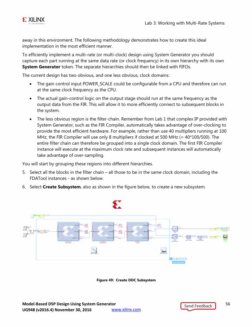
You will start by grouping these regions into different hierarchies.
5. Select all the blocks in the filter chain – all those to be in the same clock domain, including the
FDATool instances - as shown below.
6. Select Create Subsystem, also as shown in the figure below, to create a new subsystem.
Figure 49: Create DDC Subsystem
Send FeedbackUG948 (v2016.4) November 30, 2016
Lab 3: Working with Multi-Rate Systems
Model-Based DSP Design Using System Generator 57 UG948 (v2016.3) October 28, 2016 www.xilinx.com
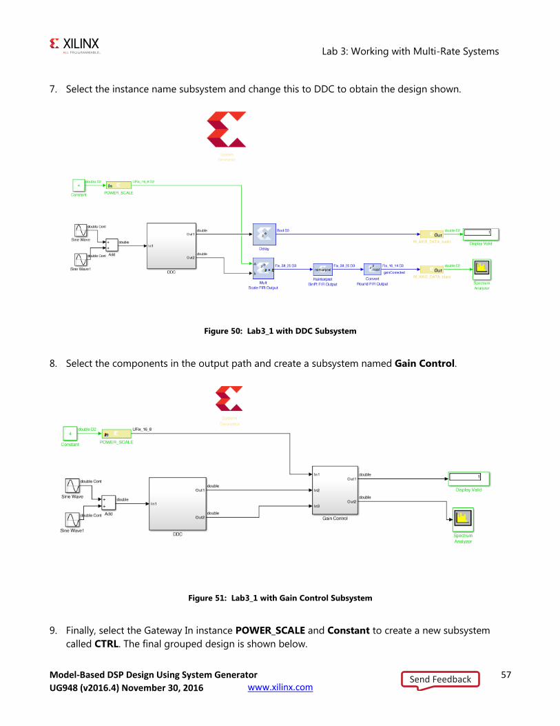
7. Select the instance name subsystem and change this to DDC to obtain the design shown.
Figure 50: Lab3_1 with DDC Subsystem
8. Select the components in the output path and create a subsystem named Gain Control.
Figure 51: Lab3_1 with Gain Control Subsystem
9. Finally, select the Gateway In instance POWER_SCALE and Constant to create a new subsystem
called CTRL. The final grouped design is shown below.
Send FeedbackUG948 (v2016.4) November 30, 2016
Lab 3: Working with Multi-Rate Systems
Model-Based DSP Design Using System Generator 58 UG948 (v2016.3) October 28, 2016 www.xilinx.com
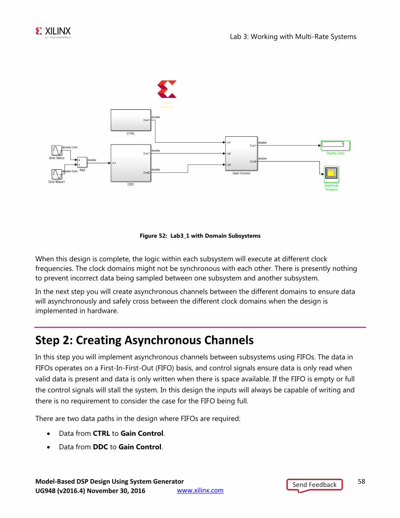
Figure 52: Lab3_1 with Domain Subsystems
When this design is complete, the logic within each subsystem will execute at different clock
frequencies. The clock domains might not be synchronous with each other. There is presently nothing
to prevent incorrect data being sampled between one subsystem and another subsystem.
In the next step you will create asynchronous channels between the different domains to ensure data
will asynchronously and safely cross between the different clock domains when the design is
implemented in hardware.
Step 2: Creating Asynchronous Channels In this step you will implement asynchronous channels between subsystems using FIFOs. The data in
FIFOs operates on a First-In-First-Out (FIFO) basis, and control signals ensure data is only read when
valid data is present and data is only written when there is space available. If the FIFO is empty or full
the control signals will stall the system. In this design the inputs will always be capable of writing and
there is no requirement to consider the case for the FIFO being full.
There are two data paths in the design where FIFOs are required:
Data from CTRL to Gain Control.
Data from DDC to Gain Control.
Send FeedbackUG948 (v2016.4) November 30, 2016
Lab 3: Working with Multi-Rate Systems
Model-Based DSP Design Using System Generator 59 UG948 (v2016.3) October 28, 2016 www.xilinx.com
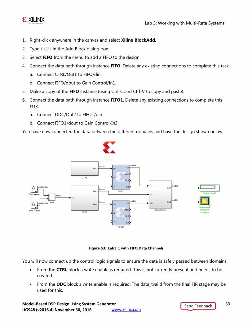
1. Right-click anywhere in the canvas and select Xilinx BlockAdd.
2. Type FIFO in the Add Block dialog box.
3. Select FIFO from the menu to add a FIFO to the design.
4. Connect the data path through instance FIFO. Delete any existing connections to complete this task.
a. Connect CTRL/Out1 to FIFO/din.
b. Connect FIFO/dout to Gain Control/In1.
5. Make a copy of the FIFO instance (using Ctrl-C and Ctrl-V to copy and paste).
6. Connect the data path through instance FIFO1. Delete any existing connections to complete this
task.
a. Connect DDC/Out2 to FIFO1/din.
b. Connect FIFO1/dout to Gain Control/In3.
You have now connected the data between the different domains and have the design shown below.
Figure 53: Lab3_1 with FIFO Data Channels
You will now connect up the control logic signals to ensure the data is safely passed between domains.
From the CTRL block a write enable is required. This is not currently present and needs to be
created.
From the DDC block a write enable is required. The data_tvalid from the final FIR stage may be
used for this.
Send FeedbackUG948 (v2016.4) November 30, 2016

Lab 3: Working with Multi-Rate Systems
Model-Based DSP Design Using System Generator 60 UG948 (v2016.3) October 28, 2016 www.xilinx.com
The Gain Control must generate a read enable for both FIFOs. You will use the empty signal
from the FIFOs and invert it; if there is data available, this block will read it.
7. Double-click the CTRL block to open the subsystem.
8. Right-click in the canvas and use Xilinx BlockAdd to add these blocks:
a. Delay (Xilinx)
b. Relational
9. Select instance Out1 and make a copy (use Ctrl-C and Ctrl-V to cut and paste).
10. Double-click the Relational block to open the Properties Editor.
11. Use the Comparison drop-down menu to select a!=b and click OK.
12. Connect the blocks as shown in the following figure.
Figure 54: Modified CTRL Subsystem
This will create an output strobe on Out2 which will be active for one cycle when the input changes. This
will be used as the write-enable from CTRL to the Gain Control (the FIFO block at the top level).
13. Click the Up to Parent toolbar button to return to the top level.
14. Double-click the instance Gain Control to open the subsystem.
15. Right-click in the canvas and use Xilinx BlockAdd to add these blocks:
a. Inverter
b. Inverter (for a total of two inverters)
c. Delay (Xilinx)
16. Select the instance Out1 and make a copy Out3 (use Ctrl-C and Ctrl-V to cut and paste).
a. Rename Out3 to DDC_Read
17. Select instance Out1 and make a copy Out3 (use Ctrl-C and Ctrl-V to cut and paste).
a. Rename Out3 to CTRL_Read
Send FeedbackUG948 (v2016.4) November 30, 2016
Lab 3: Working with Multi-Rate Systems
Model-Based DSP Design Using System Generator 61 UG948 (v2016.3) October 28, 2016 www.xilinx.com
18. Select instance In1 and make a copy In4 (use Ctrl-C and Ctrl-V to cut and paste).
a. Rename In4 to CTRL_Empty
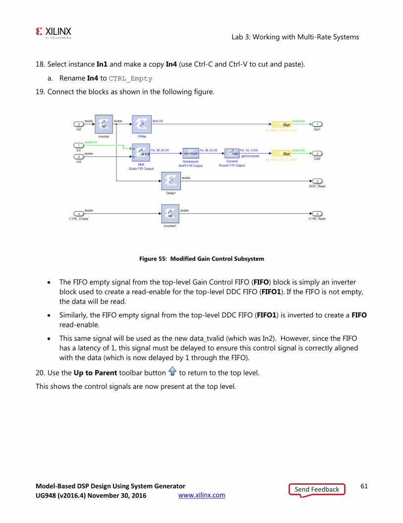
19. Connect the blocks as shown in the following figure.
Figure 55: Modified Gain Control Subsystem
The FIFO empty signal from the top-level Gain Control FIFO (FIFO) block is simply an inverter
block used to create a read-enable for the top-level DDC FIFO (FIFO1). If the FIFO is not empty,
the data will be read.
Similarly, the FIFO empty signal from the top-level DDC FIFO (FIFO1) is inverted to create a FIFO
read-enable.
This same signal will be used as the new data_tvalid (which was In2). However, since the FIFO
has a latency of 1, this signal must be delayed to ensure this control signal is correctly aligned
with the data (which is now delayed by 1 through the FIFO).
20. Use the Up to Parent toolbar button to return to the top level.
This shows the control signals are now present at the top level.
Send FeedbackUG948 (v2016.4) November 30, 2016

Lab 3: Working with Multi-Rate Systems
Model-Based DSP Design Using System Generator 62 UG948 (v2016.3) October 28, 2016 www.xilinx.com
Figure 56: Modified Lab3_1 Design
You will now complete the final connections.
21. Connect the control path through instance FIFO. Delete any existing connections to complete this
task.
a. Connect CTRL/Out2 to FIFO/we.
b. Connect FIFO/empty to Gain Control/CTRL_Empty.
c. Connect Gain Control/CTRL_Read to FIFO/re.
22. Connect the control path through instance FIFO1. Delete any existing connections to complete this
task.
a. Connect DDC/Out1 to FIFO1/we.
b. Connect FIFO1/empty to Gain Control/In2.
c. Connect Gain Control/DDC_Read to FIFO1/re.
Send FeedbackUG948 (v2016.4) November 30, 2016
Lab 3: Working with Multi-Rate Systems
Model-Based DSP Design Using System Generator 63 UG948 (v2016.3) October 28, 2016 www.xilinx.com
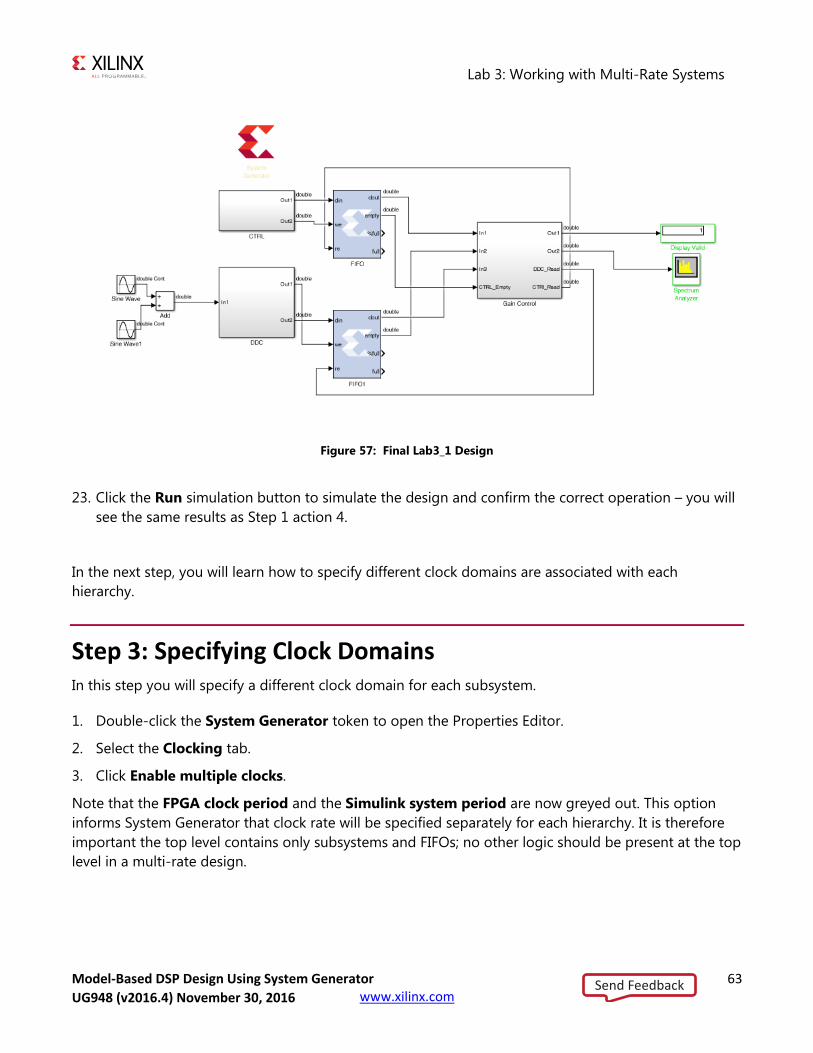
Figure 57: Final Lab3_1 Design
23. Click the Run simulation button to simulate the design and confirm the correct operation – you will
see the same results as Step 1 action 4.
In the next step, you will learn how to specify different clock domains are associated with each
hierarchy.
Step 3: Specifying Clock Domains In this step you will specify a different clock domain for each subsystem.
1. Double-click the System Generator token to open the Properties Editor.
2. Select the Clocking tab.
3. Click Enable multiple clocks.
Note that the FPGA clock period and the Simulink system period are now greyed out. This option
informs System Generator that clock rate will be specified separately for each hierarchy. It is therefore
important the top level contains only subsystems and FIFOs; no other logic should be present at the top
level in a multi-rate design.
Send FeedbackUG948 (v2016.4) November 30, 2016
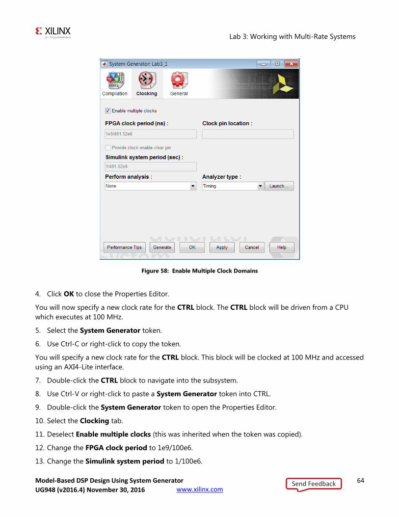
Lab 3: Working with Multi-Rate Systems
Model-Based DSP Design Using System Generator 64 UG948 (v2016.3) October 28, 2016 www.xilinx.com
Figure 58: Enable Multiple Clock Domains
4. Click OK to close the Properties Editor.
You will now specify a new clock rate for the CTRL block. The CTRL block will be driven from a CPU
which executes at 100 MHz.
5. Select the System Generator token.
6. Use Ctrl-C or right-click to copy the token.
You will specify a new clock rate for the CTRL block. This block will be clocked at 100 MHz and accessed
using an AXI4-Lite interface.
7. Double-click the CTRL block to navigate into the subsystem.
8. Use Ctrl-V or right-click to paste a System Generator token into CTRL.
9. Double-click the System Generator token to open the Properties Editor.
10. Select the Clocking tab.
11. Deselect Enable multiple clocks (this was inherited when the token was copied).
12. Change the FPGA clock period to 1e9/100e6.
13. Change the Simulink system period to 1/100e6.
Send FeedbackUG948 (v2016.4) November 30, 2016
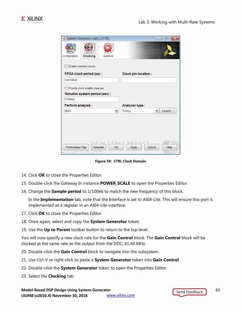
Lab 3: Working with Multi-Rate Systems
Model-Based DSP Design Using System Generator 65 UG948 (v2016.3) October 28, 2016 www.xilinx.com
Figure 59: CTRL Clock Domain
14. Click OK to close the Properties Editor.
15. Double-click the Gateway In instance POWER_SCALE to open the Properties Editor.
16. Change the Sample period to 1/100e6 to match the new frequency of this block.
In the Implementation tab, note that the Interface is set to AXI4-Lite. This will ensure this port is
implemented as a register in an AXI4-Lite interface.
17. Click OK to close the Properties Editor.
18. Once again, select and copy the System Generator token.
19. Use the Up to Parent toolbar button to return to the top level.
You will now specify a new clock rate for the Gain Control block. The Gain Control block will be
clocked at the same rate as the output from the DDC, 61.44 MHz.
20. Double-click the Gain Control block to navigate into the subsystem.
21. Use Ctrl-V or right-click to paste a System Generator token into Gain Control.
22. Double-click the System Generator token to open the Properties Editor.
23. Select the Clocking tab.
Send FeedbackUG948 (v2016.4) November 30, 2016
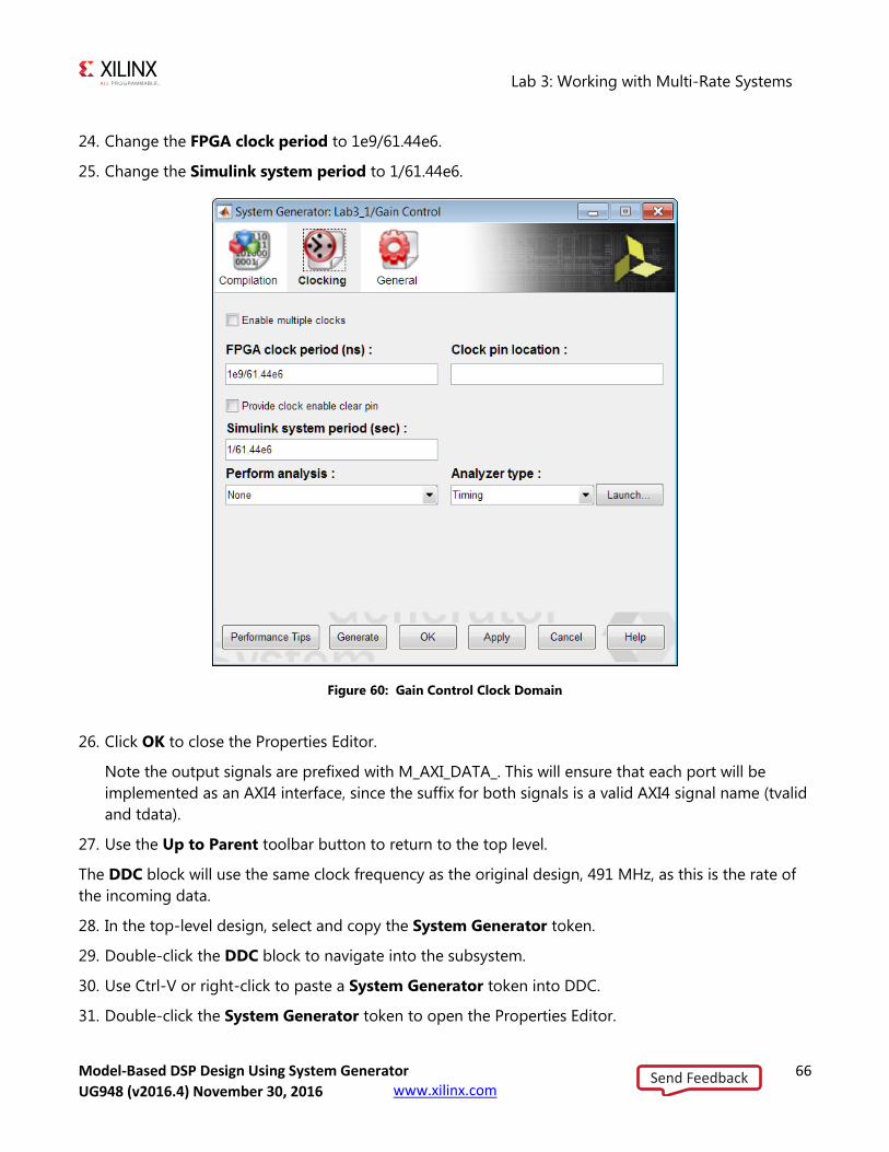
Lab 3: Working with Multi-Rate Systems
Model-Based DSP Design Using System Generator 66 UG948 (v2016.3) October 28, 2016 www.xilinx.com
24. Change the FPGA clock period to 1e9/61.44e6.
25. Change the Simulink system period to 1/61.44e6.
Figure 60: Gain Control Clock Domain
26. Click OK to close the Properties Editor.
Note the output signals are prefixed with M_AXI_DATA_. This will ensure that each port will be
implemented as an AXI4 interface, since the suffix for both signals is a valid AXI4 signal name (tvalid
and tdata).
27. Use the Up to Parent toolbar button to return to the top level.
The DDC block will use the same clock frequency as the original design, 491 MHz, as this is the rate of
the incoming data.
28. In the top-level design, select and copy the System Generator token.
29. Double-click the DDC block to navigate into the subsystem.
30. Use Ctrl-V or right-click to paste a System Generator token into DDC.
31. Double-click the System Generator token to open the Properties Editor.
Send FeedbackUG948 (v2016.4) November 30, 2016
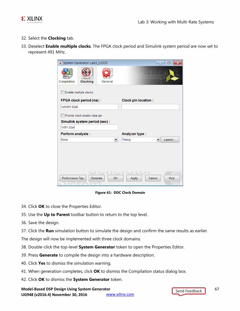
Lab 3: Working with Multi-Rate Systems
Model-Based DSP Design Using System Generator 67 UG948 (v2016.3) October 28, 2016 www.xilinx.com
32. Select the Clocking tab.
33. Deselect Enable multiple clocks. The FPGA clock period and Simulink system period are now set to
represent 491 MHz.
Figure 61: DDC Clock Domain
34. Click OK to close the Properties Editor.
35. Use the Up to Parent toolbar button to return to the top level.
36. Save the design.
37. Click the Run simulation button to simulate the design and confirm the same results as earlier.
The design will now be implemented with three clock domains.
38. Double-click the top-level System Generator token to open the Properties Editor.
39. Press Generate to compile the design into a hardware description.
40. Click Yes to dismiss the simulation warning.
41. When generation completes, click OK to dismiss the Compilation status dialog box.
42. Click OK to dismiss the System Generator token.
Send FeedbackUG948 (v2016.4) November 30, 2016
Lab 3: Working with Multi-Rate Systems
Model-Based DSP Design Using System Generator 68 UG948 (v2016.3) October 28, 2016 www.xilinx.com
43. Open the file C:\SysGen_Tutorial\Lab3\IPP_QT_MCD_0001\DDC_HB_hier\ip\hdl\
lab3_1.vhd to confirm the design is using three clocks, as shown below.
entity lab3_1 is
port (
ctrl_clk : in std_logic;
ddc_clk : in std_logic;
gain_control_clk : in std_logic;
Summary In this lab, you learned how to create separate hierarchies for portions of the design which are to be
implemented with different clock rates. You also learned how to isolate those hierarchies using FIFOs to
ensure safe asynchronous transfer of the data and how to specify the clock rates for each hierarchy.
The following solutions directory contains the final System Generator (*.slx) files for this lab. The
solutions directory does not contain the IP output from System Generator or the files and directories
generated when Vivado is executed.
C:/SysGen_Tutorial/Lab3/solution
The results from Step1 are provided in file Lab3_1_sol.slx
The results from Step2 are provided in file Lab3_2_sol.slx
The final results from Step3 are provided in file Lab3_3_sol.slx
Send FeedbackUG948 (v2016.4) November 30, 2016
Model-Based DSP Design Using System Generator 69 UG948 (v2016.3) October 28, 2016 www.xilinx.com
Lab 4: Working with Workspace Variables
Introduction In this lab, you will learn how to use workspace variables to easily parameterize your System Generator
designs.
Objectives
After completing this lab, you will be able to use workspace variables to create paramaterizable and
customizable designs.
Procedure
In this lab you will review how a design is parameterized using workspace variables.
Send FeedbackUG948 (v2016.4) November 30, 2016
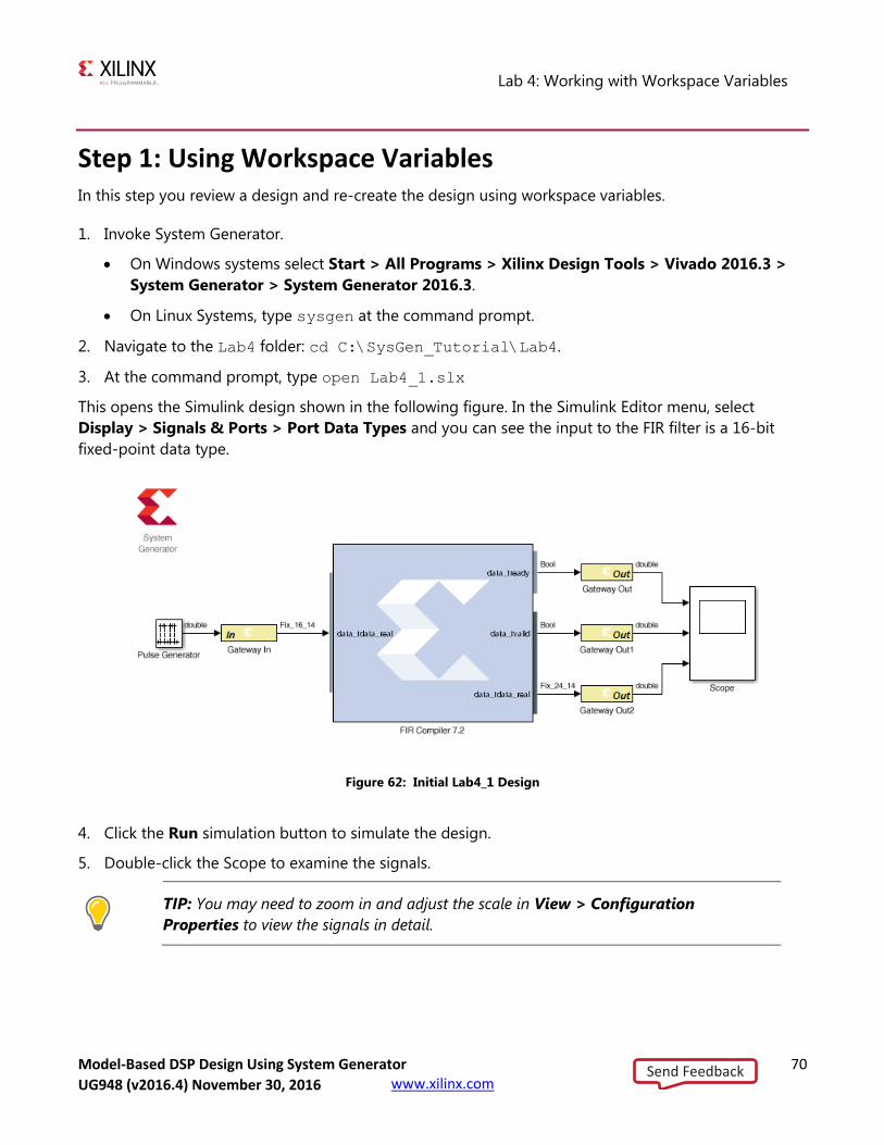
Lab 4: Working with Workspace Variables
Model-Based DSP Design Using System Generator 70 UG948 (v2016.3) October 28, 2016 www.xilinx.com
Step 1: Using Workspace Variables In this step you review a design and re-create the design using workspace variables.
1. Invoke System Generator.
On Windows systems select Start > All Programs > Xilinx Design Tools > Vivado 2016.3 >
System Generator > System Generator 2016.3.
On Linux Systems, type sysgen at the command prompt.
2. Navigate to the Lab4 folder: cd C:\SysGen_Tutorial\Lab4.
3. At the command prompt, type open Lab4_1.slx
This opens the Simulink design shown in the following figure. In the Simulink Editor menu, select
Display > Signals & Ports > Port Data Types and you can see the input to the FIR filter is a 16-bit
fixed-point data type.
Figure 62: Initial Lab4_1 Design
4. Click the Run simulation button to simulate the design.
5. Double-click the Scope to examine the signals.
TIP: You may need to zoom in and adjust the scale in View > Configuration
Properties to view the signals in detail.
Send FeedbackUG948 (v2016.4) November 30, 2016
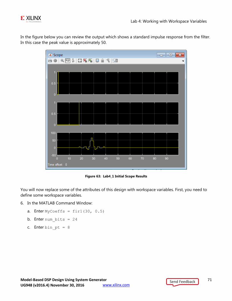
Lab 4: Working with Workspace Variables
Model-Based DSP Design Using System Generator 71 UG948 (v2016.3) October 28, 2016 www.xilinx.com
In the figure below you can review the output which shows a standard impulse response from the filter.
In this case the peak value is approximately 50.
Figure 63: Lab4_1 Initial Scope Results
You will now replace some of the attributes of this design with workspace variables. First, you need to
define some workspace variables.
6. In the MATLAB Command Window:
a. Enter MyCoeffs = fir1(30, 0.5)
b. Enter num_bits = 24
c. Enter bin_pt = 8
Send FeedbackUG948 (v2016.4) November 30, 2016
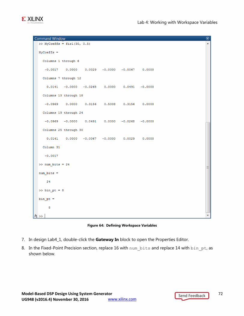
Lab 4: Working with Workspace Variables
Model-Based DSP Design Using System Generator 72 UG948 (v2016.3) October 28, 2016 www.xilinx.com
Figure 64: Defining Workspace Variables
7. In design Lab4_1, double-click the Gateway In block to open the Properties Editor.
8. In the Fixed-Point Precision section, replace 16 with num_bits and replace 14 with bin_pt, as
shown below.
Send FeedbackUG948 (v2016.4) November 30, 2016
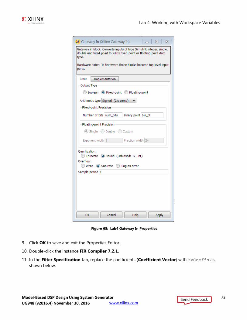
Lab 4: Working with Workspace Variables
Model-Based DSP Design Using System Generator 73 UG948 (v2016.3) October 28, 2016 www.xilinx.com
Figure 65: Lab4 Gateway In Properties
9. Click OK to save and exit the Properties Editor.
10. Double-click the instance FIR Compiler 7.2.1.
11. In the Filter Specification tab, replace the coefficients (Coefficient Vector) with MyCoeffs as
shown below.
Send FeedbackUG948 (v2016.4) November 30, 2016
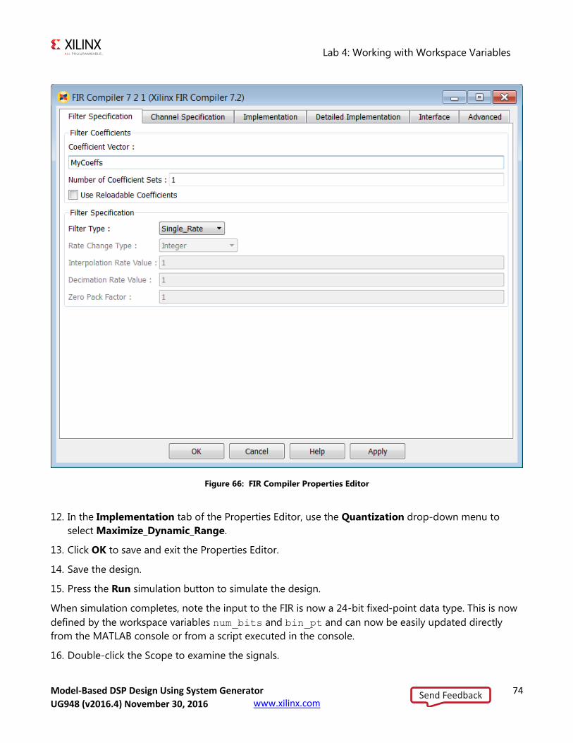
Lab 4: Working with Workspace Variables
Model-Based DSP Design Using System Generator 74 UG948 (v2016.3) October 28, 2016 www.xilinx.com
Figure 66: FIR Compiler Properties Editor
12. In the Implementation tab of the Properties Editor, use the Quantization drop-down menu to
select Maximize_Dynamic_Range.
13. Click OK to save and exit the Properties Editor.
14. Save the design.
15. Press the Run simulation button to simulate the design.
When simulation completes, note the input to the FIR is now a 24-bit fixed-point data type. This is now
defined by the workspace variables num_bits and bin_pt and can now be easily updated directly
from the MATLAB console or from a script executed in the console.
16. Double-click the Scope to examine the signals.
Send FeedbackUG948 (v2016.4) November 30, 2016

Lab 4: Working with Workspace Variables
Model-Based DSP Design Using System Generator 75 UG948 (v2016.3) October 28, 2016 www.xilinx.com
TIP: You may need to zoom in and adjust the scale in View > Configuration
Properties to view the signals in detail.
The impulse response is now defined by the values on MyCoeffs and only has a peak value of
approximately 0.5.
17. In the Lab4_1 design use File > Close > Close Model to exit the Lab4_1 design.
18. In the MATLAB console type bdclose all.
19. In the MATLAB console type clear to remove the variables from the workspace.
20. At the command prompt, type open Lab4_1.slx
21. Click the Run simulation button to simulate the design.
This results in a numbers of errors since the workspace variables are no longer defined.
22. Exit the Lab4_1.slx Simulink worksheet.
Summary In this lab, you learned how to use workspace variables to enhance your overall efficiency when using
System Generator.
Solutions to this lab can be found in the following location:
C:/SysGen_Tutorial/Lab4/solution
Send FeedbackUG948 (v2016.4) November 30, 2016
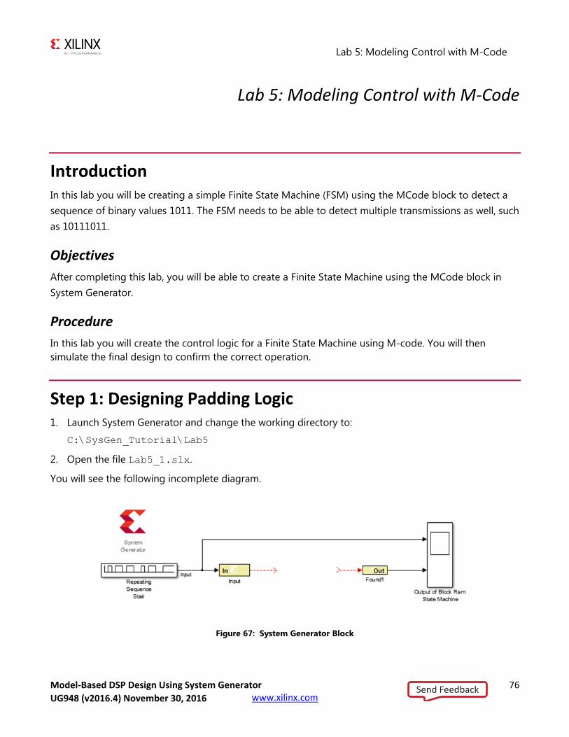
Lab 5: Modeling Control with M-Code
Model-Based DSP Design Using System Generator 76 UG948 (v2016.3) October 28, 2016 www.xilinx.com
Lab 5: Modeling Control with M-Code
Introduction In this lab you will be creating a simple Finite State Machine (FSM) using the MCode block to detect a
sequence of binary values 1011. The FSM needs to be able to detect multiple transmissions as well, such
as 10111011.
Objectives
After completing this lab, you will be able to create a Finite State Machine using the MCode block in
System Generator.
Procedure
In this lab you will create the control logic for a Finite State Machine using M-code. You will then
simulate the final design to confirm the correct operation.
Step 1: Designing Padding Logic 1. Launch System Generator and change the working directory to:
C:\SysGen_Tutorial\Lab5
2. Open the file Lab5_1.slx.
You will see the following incomplete diagram.
Figure 67: System Generator Block
Send FeedbackUG948 (v2016.4) November 30, 2016
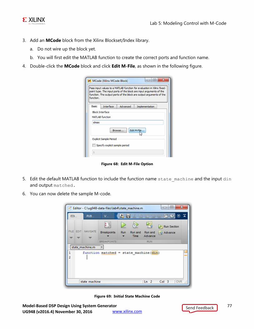
Lab 5: Modeling Control with M-Code
Model-Based DSP Design Using System Generator 77 UG948 (v2016.3) October 28, 2016 www.xilinx.com
3. Add an MCode block from the Xilinx Blockset/Index library.
a. Do not wire up the block yet.
b. You will first edit the MATLAB function to create the correct ports and function name.
4. Double-click the MCode block and click Edit M-File, as shown in the following figure.
Figure 68: Edit M-File Option
5. Edit the default MATLAB function to include the function name state_machine and the input din
and output matched.
6. You can now delete the sample M-code.
Figure 69: Initial State Machine Code
Send FeedbackUG948 (v2016.4) November 30, 2016
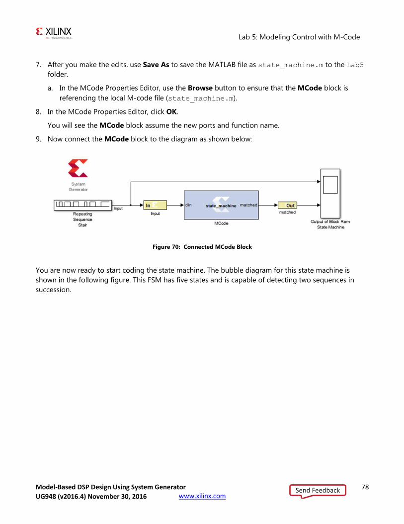
Lab 5: Modeling Control with M-Code
Model-Based DSP Design Using System Generator 78 UG948 (v2016.3) October 28, 2016 www.xilinx.com
7. After you make the edits, use Save As to save the MATLAB file as state_machine.m to the Lab5
folder.
a. In the MCode Properties Editor, use the Browse button to ensure that the MCode block is
referencing the local M-code file (state_machine.m).
8. In the MCode Properties Editor, click OK.
You will see the MCode block assume the new ports and function name.
9. Now connect the MCode block to the diagram as shown below:
Figure 70: Connected MCode Block
You are now ready to start coding the state machine. The bubble diagram for this state machine is
shown in the following figure. This FSM has five states and is capable of detecting two sequences in
succession.
Send FeedbackUG948 (v2016.4) November 30, 2016
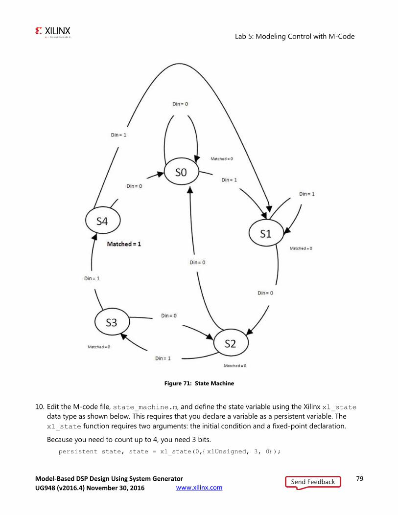
Lab 5: Modeling Control with M-Code
Model-Based DSP Design Using System Generator 79 UG948 (v2016.3) October 28, 2016 www.xilinx.com
Figure 71: State Machine
10. Edit the M-code file, state_machine.m, and define the state variable using the Xilinx xl_state
data type as shown below. This requires that you declare a variable as a persistent variable. The
xl_state function requires two arguments: the initial condition and a fixed-point declaration.
Because you need to count up to 4, you need 3 bits.
persistent state, state = xl_state(0,{xlUnsigned, 3, 0});
Send FeedbackUG948 (v2016.4) November 30, 2016

Lab 5: Modeling Control with M-Code
Model-Based DSP Design Using System Generator 80 UG948 (v2016.3) October 28, 2016 www.xilinx.com
11. Use a switch-case statement to define the FSM states shown. A small sample is provided below to
get you started.
Note: You need an otherwise statement as your last case.
switch state
case 0
if din == 1
state = 1;
else
state = 0;
end
matched = 0;
12. Save the M-code file and run the simulation. The waveform should look like the following figure.
You should notice two detections of the sequence.
Figure 72: Lab5 Waveforms
Summary In this exercise you learned how to create control logic using M-Code. The final design may be used to
create an HDL netlist, in the same manner as designs created using the Xilinx Blocksets.
Solutions to this lab can be found in the following location:
C:/SysGen_Tutorial/Lab5/solution
Send FeedbackUG948 (v2016.4) November 30, 2016

Model-Based DSP Design Using System Generator 81 UG948 (v2016.3) October 28, 2016 www.xilinx.com
Lab 6: Modeling Blocks with HDL
Introduction In this lab exercise you will import an RTL design into System Generator as a black box.
A black box allows the design to be imported into System Generator even though the
description is in Hardware Description Language (HDL) format.
Objectives
After completing this lab, you will be able to:
Import an RTL HDL description into System Generator for DSP.
Configure the black box to ensure the design can be successfully simulated.
Step 1: Import RTL as a Black Box 1. Invoke System Generator and from the MATLAB console, change the directory to:
C:\SysGen_Tutorial\Lab6
The following files are located in this directory:
Lab6_1.slx - A Simulink model containing a black box example.
transpose_fir.vhd - Top-level VHDL for a transpose form FIR filter. This file is the VHDL
that is associated with the black box.
mac.vhd – Multiply and adder component used to build the transpose FIR filter.
2. Type open Lab6_1.slx.
3. Open the subsystem named Down Converter.
4. Open the subsystem named Transpose FIR Filter Black Box.
At this point, the subsystem contains two input ports and one output port. You will add a black box
to this subsystem:
Send FeedbackUG948 (v2016.4) November 30, 2016
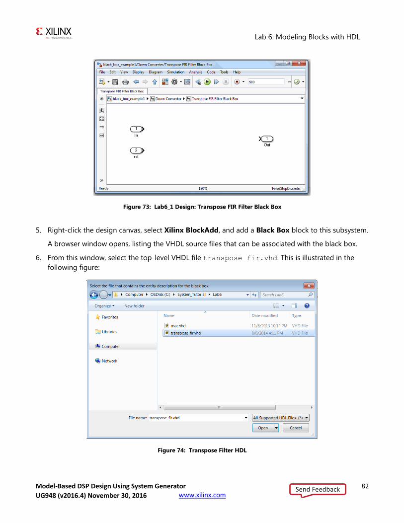
Lab 6: Modeling Blocks with HDL
Model-Based DSP Design Using System Generator 82 UG948 (v2016.3) October 28, 2016 www.xilinx.com
Figure 73: Lab6_1 Design: Transpose FIR Filter Black Box
5. Right-click the design canvas, select Xilinx BlockAdd, and add a Black Box block to this subsystem.
A browser window opens, listing the VHDL source files that can be associated with the black box.
6. From this window, select the top-level VHDL file transpose_fir.vhd. This is illustrated in the
following figure:
Figure 74: Transpose Filter HDL
Send FeedbackUG948 (v2016.4) November 30, 2016

Lab 6: Modeling Blocks with HDL
Model-Based DSP Design Using System Generator 83 UG948 (v2016.3) October 28, 2016 www.xilinx.com
The associated configuration M-code transpose_fir_config.m opens in an Editor for
modifications.
7. Close the Editor.
8. Wire the ports of the black box to the corresponding subsystem ports and save the design.
Figure 75: Transpose Filter as a Black Box
9. Double click the Black Box block to open this dialog box:
Figure 76: Black Box Properties Editor
Send FeedbackUG948 (v2016.4) November 30, 2016
Lab 6: Modeling Blocks with HDL
Model-Based DSP Design Using System Generator 84 UG948 (v2016.3) October 28, 2016 www.xilinx.com
The following are the fields in the dialog box:
Block configuration m-function: This specifies the name of the configuration M-function for
the black box. In this example, the field contains the name of the function that was generated by
the Configuration Wizard. By default, the black box uses the function the wizard produces. You
can however substitute one you create yourself.
Simulation mode: There are three simulation modes:
o Inactive: When the mode is Inactive, the black box participates in the simulation by ignoring
its inputs and producing zeros. This setting is typically used when a separate simulation
model is available for the black box, and the model is wired in parallel with the black box
using a simulation multiplexer.
o Vivado Simulator: When the mode is Vivado Simulator, simulation results for the black box
are produced using co-simulation on the HDL associated with the black box.
o External co-simulator: When the mode is External co-simulator, it is necessary to add a
ModelSim HDL co-simulation block to the design, and to specify the name of the ModelSim
block in the HDL co-simulator to use field. In this mode, the black box is simulated using
HDL co-simulation.
10. Set the Simulation mode to Inactive and click OK to close the dialog box.
11. Move to the design’s top level and run the simulation by clicking the Run simulation button ;
then double-click the Scope block.
12. Notice the black box output shown in the Output Signal scope is zero. This is expected because the
black box is configured to be Inactive during simulation.
Send FeedbackUG948 (v2016.4) November 30, 2016
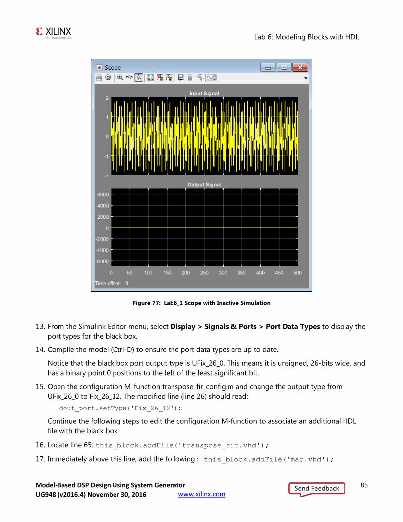
Lab 6: Modeling Blocks with HDL
Model-Based DSP Design Using System Generator 85 UG948 (v2016.3) October 28, 2016 www.xilinx.com
Figure 77: Lab6_1 Scope with Inactive Simulation
13. From the Simulink Editor menu, select Display > Signals & Ports > Port Data Types to display the
port types for the black box.
14. Compile the model (Ctrl-D) to ensure the port data types are up to date.
Notice that the black box port output type is UFix_26_0. This means it is unsigned, 26-bits wide, and
has a binary point 0 positions to the left of the least significant bit.
15. Open the configuration M-function transpose_fir_config.m and change the output type from
UFix_26_0 to Fix_26_12. The modified line (line 26) should read:
dout_port.setType('Fix_26_12');
Continue the following steps to edit the configuration M-function to associate an additional HDL
file with the black box.
16. Locate line 65: this_block.addFile('transpose_fir.vhd');
17. Immediately above this line, add the following: this_block.addFile('mac.vhd');
Send FeedbackUG948 (v2016.4) November 30, 2016
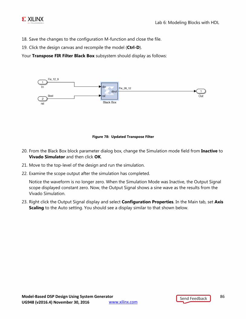
Lab 6: Modeling Blocks with HDL
Model-Based DSP Design Using System Generator 86 UG948 (v2016.3) October 28, 2016 www.xilinx.com
18. Save the changes to the configuration M-function and close the file.
19. Click the design canvas and recompile the model (Ctrl-D).
Your Transpose FIR Filter Black Box subsystem should display as follows:
Figure 78: Updated Transpose Filter
20. From the Black Box block parameter dialog box, change the Simulation mode field from Inactive to
Vivado Simulator and then click OK.
21. Move to the top-level of the design and run the simulation.
22. Examine the scope output after the simulation has completed.
Notice the waveform is no longer zero. When the Simulation Mode was Inactive, the Output Signal
scope displayed constant zero. Now, the Output Signal shows a sine wave as the results from the
Vivado Simulation.
23. Right click the Output Signal display and select Configuration Properties. In the Main tab, set Axis
Scaling to the Auto setting. You should see a display similar to that shown below.
Send FeedbackUG948 (v2016.4) November 30, 2016
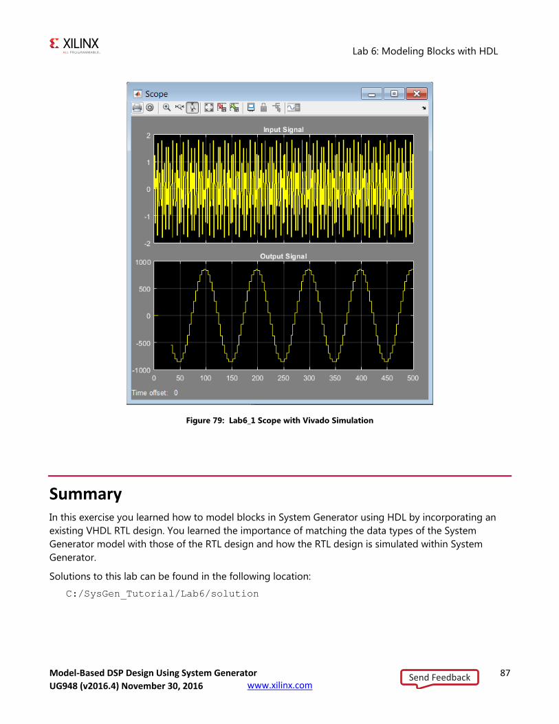
Lab 6: Modeling Blocks with HDL
Model-Based DSP Design Using System Generator 87 UG948 (v2016.3) October 28, 2016 www.xilinx.com
Figure 79: Lab6_1 Scope with Vivado Simulation
Summary In this exercise you learned how to model blocks in System Generator using HDL by incorporating an
existing VHDL RTL design. You learned the importance of matching the data types of the System
Generator model with those of the RTL design and how the RTL design is simulated within System
Generator.
Solutions to this lab can be found in the following location:
C:/SysGen_Tutorial/Lab6/solution
Send FeedbackUG948 (v2016.4) November 30, 2016
Model-Based DSP Design Using System Generator 88 UG948 (v2016.3) October 28, 2016 www.xilinx.com
Lab 7: Modeling Blocks with C Code
Introduction The System Edition of the Vivado® Design Environment includes the Vivado HLS feature, which has the
ability to transform C/C++ design sources into RTL. System Generator has a Vivado HLS block in the
Xilinx Blockset/Control Logic and Xilinx Blockset/Index libraries that enables you to bring in C/C++
source files into a System Generator model.
Objectives
After completing this lab, you will be able to incorporate a design, synthesized from C, C++ or SystemC
using Vivado HLS, as a block into your MATLAB design.
Procedure
In this exercise you will first synthesize a C file using Vivado HLS. You will operate within a Vivado DSP
design project, using a design file from MATLAB along with an associated HDL wrapper and constraint
file. In Step 2, you incorporate the output from Vivado HLS into MATLAB and use the rich simulation
features of MATLAB to verify that the C algorithm correctly filters an image.
Send FeedbackUG948 (v2016.4) November 30, 2016
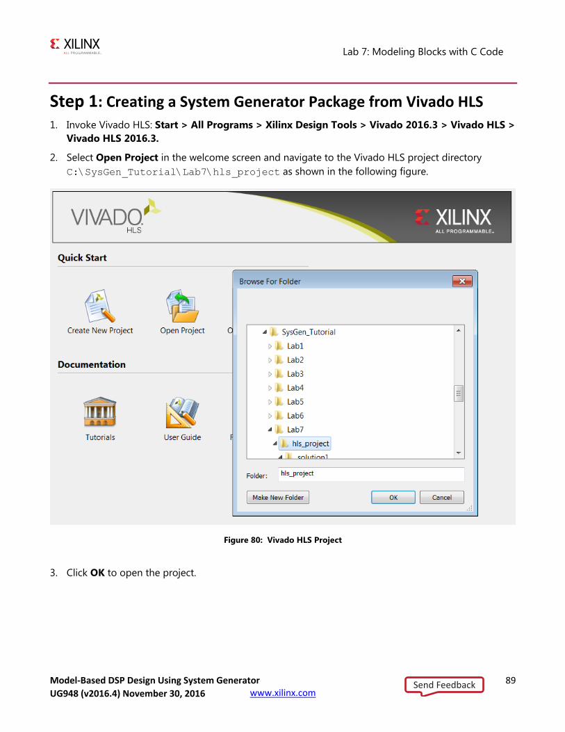
Lab 7: Modeling Blocks with C Code
Model-Based DSP Design Using System Generator 89 UG948 (v2016.3) October 28, 2016 www.xilinx.com
Step 1: Creating a System Generator Package from Vivado HLS 1. Invoke Vivado HLS: Start > All Programs > Xilinx Design Tools > Vivado 2016.3 > Vivado HLS >
Vivado HLS 2016.3.
2. Select Open Project in the welcome screen and navigate to the Vivado HLS project directory
C:\SysGen_Tutorial\Lab7\hls_project as shown in the following figure.
Figure 80: Vivado HLS Project
3. Click OK to open the project.
Send FeedbackUG948 (v2016.4) November 30, 2016
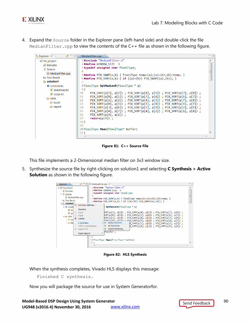
Lab 7: Modeling Blocks with C Code
Model-Based DSP Design Using System Generator 90 UG948 (v2016.3) October 28, 2016 www.xilinx.com
4. Expand the Source folder in the Explorer pane (left-hand side) and double-click the file
MedianFilter.cpp to view the contents of the C++ file as shown in the following figure.
Figure 81: C++ Source File
This file implements a 2-Dimensional median filter on 3x3 window size.
5. Synthesize the source file by right-clicking on solution1 and selecting C Synthesis > Active
Solution as shown in the following figure.
Figure 82: HLS Synthesis
When the synthesis completes, Vivado HLS displays this message:
Finished C synthesis.
Now you will package the source for use in System Generatorfor.
Send FeedbackUG948 (v2016.4) November 30, 2016

Lab 7: Modeling Blocks with C Code
Model-Based DSP Design Using System Generator 91 UG948 (v2016.3) October 28, 2016 www.xilinx.com
6. Right-click solution1 and select Export RTL.
7. Set Format Selection to System Generator for DSP as shown in the following figure and click OK.
Figure 83: Export HLS IP to System Generator
When the Export RTL process completes, Vivado HLS displays this message:
Finished export RTL.
8. Exit Vivado HLS.
Send FeedbackUG948 (v2016.4) November 30, 2016
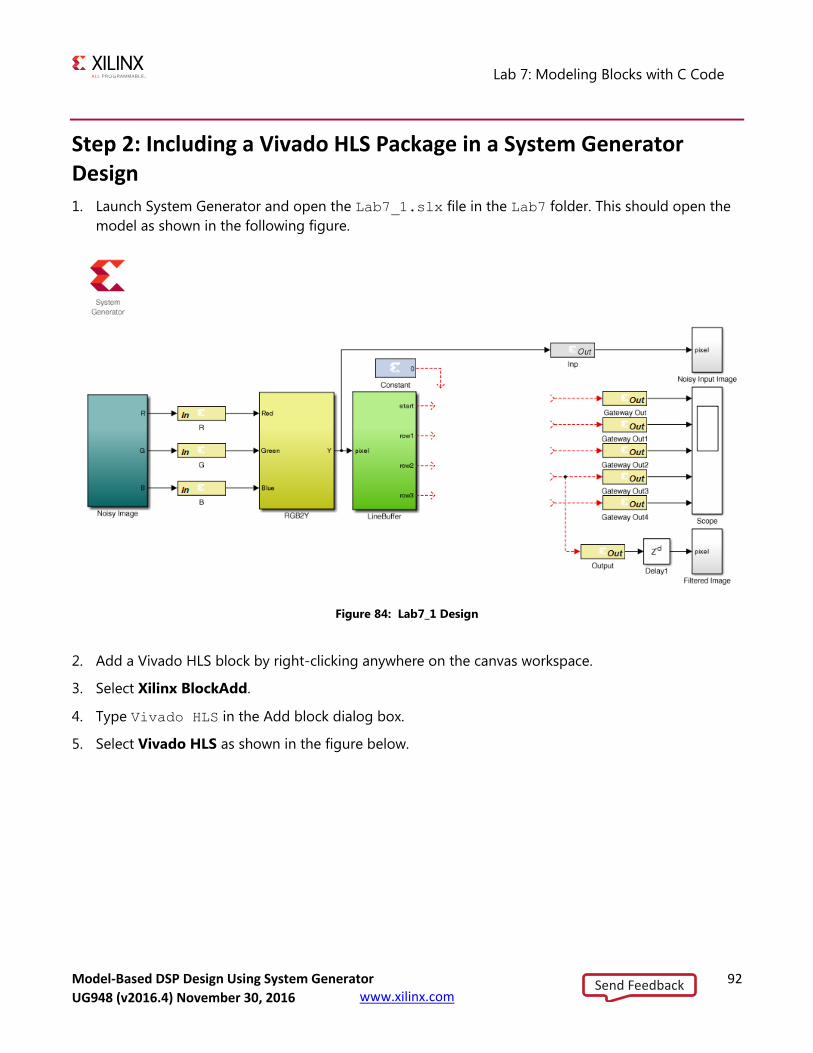
Lab 7: Modeling Blocks with C Code
Model-Based DSP Design Using System Generator 92 UG948 (v2016.3) October 28, 2016 www.xilinx.com
Step 2: Including a Vivado HLS Package in a System Generator Design
1. Launch System Generator and open the Lab7_1.slx file in the Lab7 folder. This should open the
model as shown in the following figure.
Figure 84: Lab7_1 Design
2. Add a Vivado HLS block by right-clicking anywhere on the canvas workspace.
3. Select Xilinx BlockAdd.
4. Type Vivado HLS in the Add block dialog box.
5. Select Vivado HLS as shown in the figure below.
Send FeedbackUG948 (v2016.4) November 30, 2016
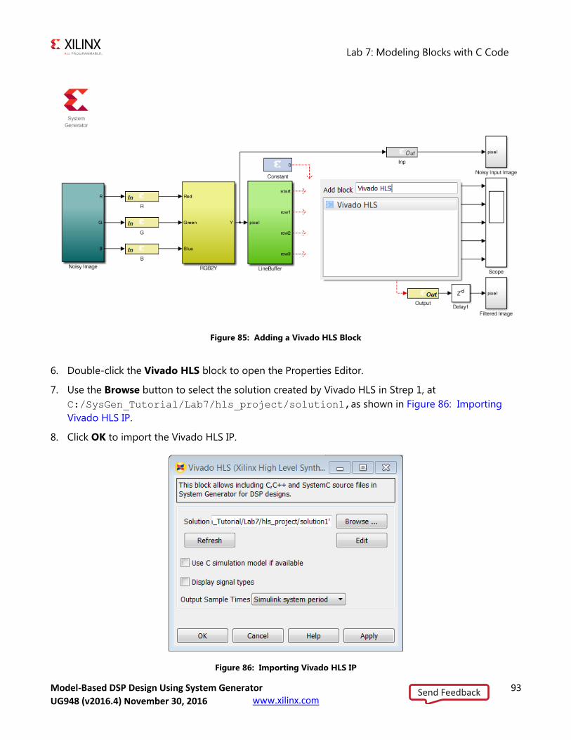
Lab 7: Modeling Blocks with C Code
Model-Based DSP Design Using System Generator 93 UG948 (v2016.3) October 28, 2016 www.xilinx.com
Figure 85: Adding a Vivado HLS Block
6. Double-click the Vivado HLS block to open the Properties Editor.
7. Use the Browse button to select the solution created by Vivado HLS in Strep 1, at
C:/SysGen_Tutorial/Lab7/hls_project/solution1,as shown in Figure 86: Importing
Vivado HLS IP.
8. Click OK to import the Vivado HLS IP.
Figure 86: Importing Vivado HLS IP
Send FeedbackUG948 (v2016.4) November 30, 2016
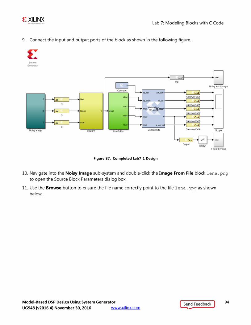
Lab 7: Modeling Blocks with C Code
Model-Based DSP Design Using System Generator 94 UG948 (v2016.3) October 28, 2016 www.xilinx.com
9. Connect the input and output ports of the block as shown in the following figure.
Figure 87: Completed Lab7_1 Design
10. Navigate into the Noisy Image sub-system and double-click the Image From File block lena.png
to open the Source Block Parameters dialog box.
11. Use the Browse button to ensure the file name correctly point to the file lena.jpg as shown
below.
Send FeedbackUG948 (v2016.4) November 30, 2016
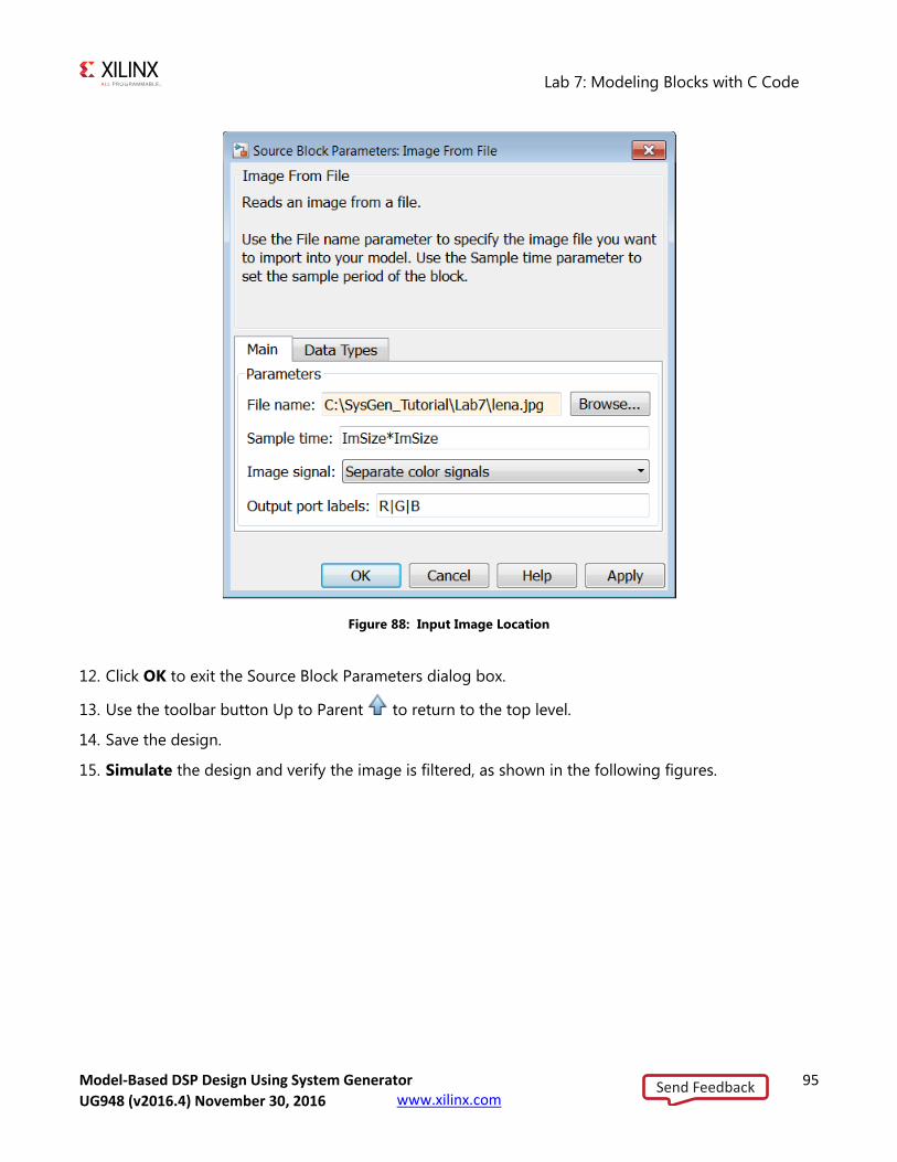
Lab 7: Modeling Blocks with C Code
Model-Based DSP Design Using System Generator 95 UG948 (v2016.3) October 28, 2016 www.xilinx.com
Figure 88: Input Image Location
12. Click OK to exit the Source Block Parameters dialog box.
13. Use the toolbar button Up to Parent to return to the top level.
14. Save the design.
15. Simulate the design and verify the image is filtered, as shown in the following figures.
Send FeedbackUG948 (v2016.4) November 30, 2016
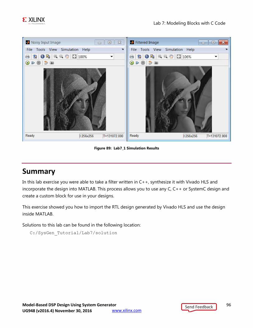
Lab 7: Modeling Blocks with C Code
Model-Based DSP Design Using System Generator 96 UG948 (v2016.3) October 28, 2016 www.xilinx.com
Figure 89: Lab7_1 Simulation Results
Summary In this lab exercise you were able to take a filter written in C++, synthesize it with Vivado HLS and
incorporate the design into MATLAB. This process allows you to use any C, C++ or SystemC design and
create a custom block for use in your designs.
This exercise showed you how to import the RTL design generated by Vivado HLS and use the design
inside MATLAB.
Solutions to this lab can be found in the following location:
C:/SysGen_Tutorial/Lab7/solution
Send FeedbackUG948 (v2016.4) November 30, 2016

Model-Based DSP Design Using System Generator 97 UG948 (v2016.3) October 28, 2016 www.xilinx.com
Lab 8: Using AXI Interfaces and IP Integrator
Introduction In this lab, you will learn how AXI interfaces are implemented using System Generator. You will save the
design in IP catalog format and use the resulting IP in the Vivado IP Integrator environment. Then you
will see how IP Integrator enhances your productively by supplying connection assistance when you use
AXI interfaces.
Objectives
After completing this lab, you will be able to:
Implement AXI interfaces in your designs.
Add your design as IP in the Vivado IP Catalog.
Connect your design in IP Integrator.
Procedure
This exercise has four primary parts.
In Step 1, you will review how AXI interfaces are implemented using System Generator.
In Step 2, you will create a Vivado project for your System Generator IP.
In Step 3, you will create a design in IP Integrator using the System Generator IP.
In Step 4, you will implement the design and generate an FPGA bitstream (the file used to
program the FPGA).
Send FeedbackUG948 (v2016.4) November 30, 2016

Lab 8: Using AXI Interfaces and IP Integrator
Model-Based DSP Design Using System Generator 98 UG948 (v2016.3) October 28, 2016 www.xilinx.com
Step 1: Review the AXI Interfaces In this step you review how AXI interfaces are defined and created.
1. Invoke System Generator and use the Current Folder browser to change the directory to C:\SysGen_Tutorial\Lab8.
2. Type open Lab8_1.slx in the Command Window.
This opens the design shown in the following figure.
Figure 90: Lab8_1 Design
This design uses a number of AXI interfaces. You will review these shortly.
Using AXI interfaces allows a design exported to the Vivado IP Catalog to be efficiently integrated
into a larger system using IP Integrator.
It is not a requirement for designs exported to the IP Catalog to use AXI interfaces.
This design uses the following AXI interfaces:
An AXI4-Stream interface is used for ports s_axis_source_*. All Gateway In and Out signals are
prefixed with the same name (s_axis_source_), ensuring they are grouped into the same
interface. The suffixes for all ports are valid AXI4-Stream interface signal names (tready, tvalid,
tlast and tdata).
Similarly, an AXI4-Stream interface is used for ports m_axis_dout_*.
An AXI4-Lite interface is used for the remaining ports. You can confirm this using the following
steps:
3. Double-click Gateway In instance decrypt (or any of reset, Keys[63:32], Keys[31:0], or parity_err).
Send FeedbackUG948 (v2016.4) November 30, 2016

Lab 8: Using AXI Interfaces and IP Integrator
Model-Based DSP Design Using System Generator 99 UG948 (v2016.3) October 28, 2016 www.xilinx.com
4. In the Properties Editor select the Implementation tab.
5. Confirm the Interface is specified as AXI4-Lite in the Interface options.
6. Click OK to exit the Properties Editor.
Details on simulating the design are provided in the canvas notes. For this exercise, you will
concentrate on exporting the design to the Vivado IP catalog and use the IP in an existing design.
Step 2: Create a Vivado Project using System Generator IP In this step you create a Vivado project which you will use to create your hardware design.
1. Double-click the System Generator token to open the Properties Editor.
2. In the Properties Editor, make sure IP Catalog is selected for the Compilation type.
3. Click Generate to generate a design in IP Catalog format.
4. Click OK to dismiss the Compilation status dialog box.
5. Click OK to dismiss the System Generator token.
The design has been written in IP Catalog format to the directory ./sys_gen_ip. You will now
import this IP into the Vivado IP Catalog and use the IP in an existing example project.
6. Open the Vivado IDE using Start > All Programs > Xilinx Design Tools > Vivado 2016.3 >
Vivado 2016.3.
7. Click Create New Project.
8. Click Next.
9. Specify the project location as C:/SysGen_Tutorial/Lab8/IPI_Project.
TIP: You will have to manually type /IPI_Project in the Project location box to
create the IPI_Project directory.
Send FeedbackUG948 (v2016.4) November 30, 2016

Lab 8: Using AXI Interfaces and IP Integrator
Model-Based DSP Design Using System Generator 100 UG948 (v2016.3) October 28, 2016 www.xilinx.com
Figure 91: Vivado IPI Project
10. Click Next.
11. Select both RTL Project and Do not specify sources at this time and click Next.
12. Select Boards and ZYNQ-7 ZC702 Evaluation Board as shown in the next figure.
Send FeedbackUG948 (v2016.4) November 30, 2016
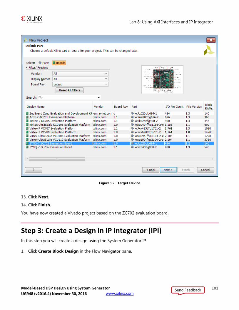
Lab 8: Using AXI Interfaces and IP Integrator
Model-Based DSP Design Using System Generator 101 UG948 (v2016.3) October 28, 2016 www.xilinx.com
Figure 92: Target Device
13. Click Next.
14. Click Finish.
You have now created a Vivado project based on the ZC702 evaluation board.
Step 3: Create a Design in IP Integrator (IPI) In this step you will create a design using the System Generator IP.
1. Click Create Block Design in the Flow Navigator pane.
Send FeedbackUG948 (v2016.4) November 30, 2016

Lab 8: Using AXI Interfaces and IP Integrator
Model-Based DSP Design Using System Generator 102 UG948 (v2016.3) October 28, 2016 www.xilinx.com
Figure 93: Open Block Design
2. In the Create Block Design dialog box, click OK to accept the default name.
You will first create an IP repository for the System Generator IP and add the IP to the repository.
3. Click the IP Setting button as shown below.
Figure 94: Open IP Settings
Send FeedbackUG948 (v2016.4) November 30, 2016
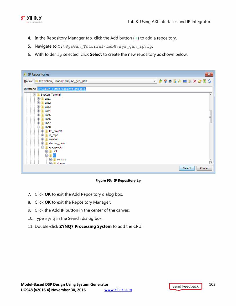
Lab 8: Using AXI Interfaces and IP Integrator
Model-Based DSP Design Using System Generator 103 UG948 (v2016.3) October 28, 2016 www.xilinx.com
4. In the Repository Manager tab, click the Add button (+) to add a repository.
5. Navigate to C:\SysGen_Tutorial\Lab8\sys_gen_ip\ip.
6. With folder ip selected, click Select to create the new repository as shown below.
Figure 95: IP Repository ip
7. Click OK to exit the Add Repository dialog box.
8. Click OK to exit the Repository Manager.
9. Click the Add IP button in the center of the canvas.
10. Type zynq in the Search dialog box.
11. Double-click ZYNQ7 Processing System to add the CPU.
Send FeedbackUG948 (v2016.4) November 30, 2016
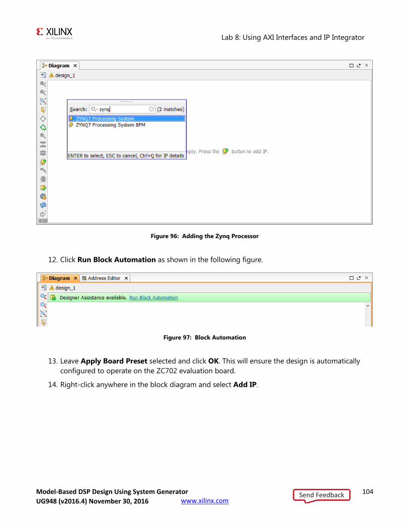
Lab 8: Using AXI Interfaces and IP Integrator
Model-Based DSP Design Using System Generator 104 UG948 (v2016.3) October 28, 2016 www.xilinx.com
Figure 96: Adding the Zynq Processor
12. Click Run Block Automation as shown in the following figure.
Figure 97: Block Automation
13. Leave Apply Board Preset selected and click OK. This will ensure the design is automatically
configured to operate on the ZC702 evaluation board.
14. Right-click anywhere in the block diagram and select Add IP.
Send FeedbackUG948 (v2016.4) November 30, 2016
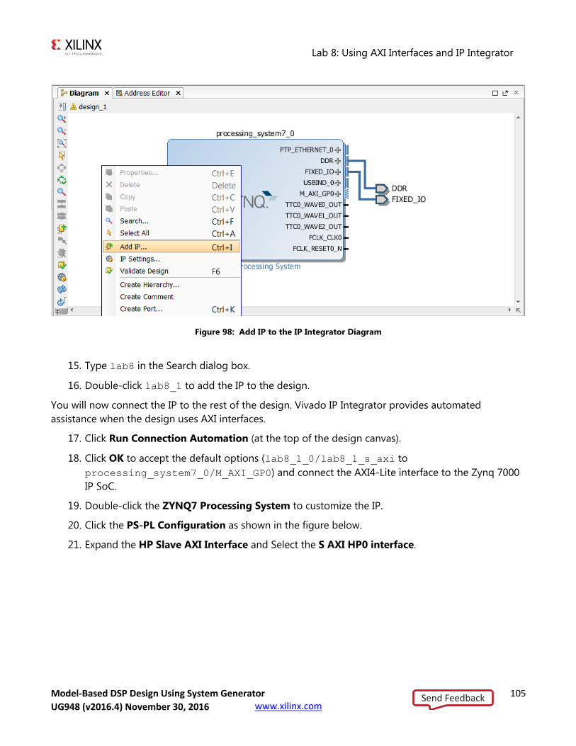
Lab 8: Using AXI Interfaces and IP Integrator
Model-Based DSP Design Using System Generator 105 UG948 (v2016.3) October 28, 2016 www.xilinx.com
Figure 98: Add IP to the IP Integrator Diagram
15. Type lab8 in the Search dialog box.
16. Double-click lab8_1 to add the IP to the design.
You will now connect the IP to the rest of the design. Vivado IP Integrator provides automated
assistance when the design uses AXI interfaces.
17. Click Run Connection Automation (at the top of the design canvas).
18. Click OK to accept the default options (lab8_1_0/lab8_1_s_axi to
processing_system7_0/M_AXI_GP0) and connect the AXI4-Lite interface to the Zynq 7000
IP SoC.
19. Double-click the ZYNQ7 Processing System to customize the IP.
20. Click the PS-PL Configuration as shown in the figure below.
21. Expand the HP Slave AXI Interface and Select the S AXI HP0 interface.
Send FeedbackUG948 (v2016.4) November 30, 2016
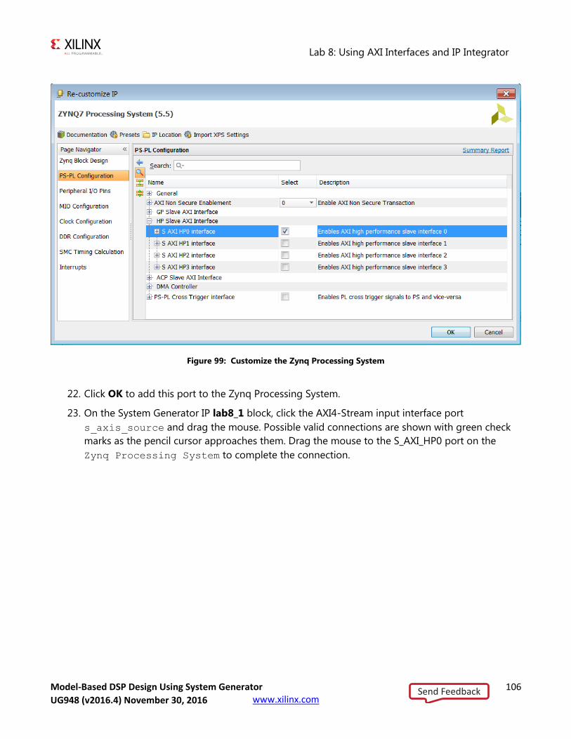
Lab 8: Using AXI Interfaces and IP Integrator
Model-Based DSP Design Using System Generator 106 UG948 (v2016.3) October 28, 2016 www.xilinx.com
Figure 99: Customize the Zynq Processing System
22. Click OK to add this port to the Zynq Processing System.
23. On the System Generator IP lab8_1 block, click the AXI4-Stream input interface port
s_axis_source and drag the mouse. Possible valid connections are shown with green check
marks as the pencil cursor approaches them. Drag the mouse to the S_AXI_HP0 port on the
Zynq Processing System to complete the connection.
Send FeedbackUG948 (v2016.4) November 30, 2016
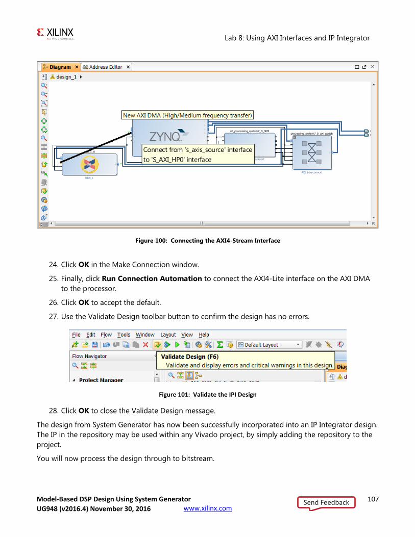
Lab 8: Using AXI Interfaces and IP Integrator
Model-Based DSP Design Using System Generator 107 UG948 (v2016.3) October 28, 2016 www.xilinx.com
Figure 100: Connecting the AXI4-Stream Interface
24. Click OK in the Make Connection window.
25. Finally, click Run Connection Automation to connect the AXI4-Lite interface on the AXI DMA
to the processor.
26. Click OK to accept the default.
27. Use the Validate Design toolbar button to confirm the design has no errors.
Figure 101: Validate the IPI Design
28. Click OK to close the Validate Design message.
The design from System Generator has now been successfully incorporated into an IP Integrator design.
The IP in the repository may be used within any Vivado project, by simply adding the repository to the
project.
You will now process the design through to bitstream.
Send FeedbackUG948 (v2016.4) November 30, 2016

Lab 8: Using AXI Interfaces and IP Integrator
Model-Based DSP Design Using System Generator 108 UG948 (v2016.3) October 28, 2016 www.xilinx.com
Step 4: Implement the Design In this step you will implement the IPI design and generate a bitsteam.
1. Return to the Project Manager view by clicking Project Manager in the Flow Navigator.
2. In the Sources browser in the main workspace pane, a Block Diagram object called design_1 is at
the top of the Design Sources tree view.
3. Right-click this object and select Generate Output Products.
Figure 102: Generate Output Products
4. In the Generate Output Products dialog box, click Generate to start the process of generating the
necessary source files.
5. When the generation completes, right-click the design_1 object again, select Create HDL
Wrapper, and click OK (and let Vivado manage the wrapper) to exit the resulting dialog box.
The top level of the Design Sources tree becomes the design_1_wrapper.v file. The design is now
ready to be synthesized, implemented, and to have an FPGA programming bitstream generated.
6. In the Flow Navigator, click Generate Bitstream to initiate the remainder of the flow.
7. Click Yes to generate the synthesis and implementation files.
8. In the dialog that appears after bitstream generation has completed, select Open Implemented
Design and click OK.
9. Exit the Vivado IDE.
The next tutorial: Lab 9: Using a System Generator Design with a Zynq-7000 AP SoC, shows how this
design may be further processed using the Vivado IDE to implement this design with software on a
Xilinx ZC702 evaluation board.
Send FeedbackUG948 (v2016.4) November 30, 2016
Lab 8: Using AXI Interfaces and IP Integrator
Model-Based DSP Design Using System Generator 109 UG948 (v2016.3) October 28, 2016 www.xilinx.com
Summary In this lab, you learned how AXI interfaces are added to a System Generator design and how a System
Generator design is saved in IP Catalog format, incorporated into the Vivado IP Catalog, and used in a
larger design. You also saw how IP Integrator can substantially increase productivity with connection
automation and hints when AXI interfaces are used in your design.
The following solutions directory contains the final System Generator (*.slx) files for this lab. The
solutions directory does not contain the IP output from System Generator or the files and directories
generated when Vivado is executed.
C:/SysGen_Tutorial/Lab8/solution
Send FeedbackUG948 (v2016.4) November 30, 2016

Model-Based DSP Design Using System Generator 110 UG948 (v2016.3) October 28, 2016 www.xilinx.com
Lab 9: Using a System Generator Design with a Zynq-7000 AP SoC
Introduction In this lab, you will learn how to export your Vivado design with System Generator IP to a software
environment and use driver files created by System Generator to quickly implement your project on a
Xilinx evaluation board, running hardware with software in the same design.
Objectives
After completing this lab, you will be able to:
Understand how to export your Vivado design with System Generator IP to a software
environment (SDK).
Understand how System Generator automatically creates software driver files for AXI4-Lite
interfaces.
Understand how to integrate the System Generator driver files into your software application.
Procedure
This exercise has two primary parts.
In Step 1, you will review the AXI4-Lite interface and associated C drivers.
In Step 2, you will export your Vivado design to a software environment and run it on a board.
Send FeedbackUG948 (v2016.4) November 30, 2016
Lab 9: Using a System Generator Design with a Zynq-7000 AP SoC
Model-Based DSP Design Using System Generator 111 UG948 (v2016.3) October 28, 2016 www.xilinx.com
Step 1: Review the AXI4-Lite Interface Drivers In this step you review how AXI4-Lite interface drivers are provided when a design with an AXI4-Lite
interface is saved.
This exercise uses the same design as Lab 8: Using AXI Interfaces and IP Integrator.
1. Invoke System Generator and use the Current Folder browser to change the directory to:
C:\SysGen_Tutorial\Lab9.
2. At the command prompt, type open Lab9_1.slx.
This opens the design shown in the following figure.
Figure 103: Lab9_1 Design
This design uses a number of AXI interfaces. These interfaces were reviewed in Lab 8 and the review is
repeated here with additional details on the AXI4-Lite register addressing.
Using AXI interfaces allows a design exported to the Vivado IP Catalog to be efficiently
integrated into a greater system using IP integrator.
It is not a requirement for designs exported to the IP Catalog to use AXI interfaces.
The design uses the following AXI interfaces:
An AXI4-Stream interface is used for ports s_axis_source_*. All Gateway In and Out signals
are prefixed with same name (s_axis_source_) ensuring they are grouped into the same
interface. The suffix for all ports are valid AXI4-Stream interface signal names (tvalid, tlast
and tdata).
An AXI4-Lite interface is used for the remaining ports. You can confirm this by performing the
following steps:
Send FeedbackUG948 (v2016.4) November 30, 2016
Lab 9: Using a System Generator Design with a Zynq-7000 AP SoC
Model-Based DSP Design Using System Generator 112 UG948 (v2016.3) October 28, 2016 www.xilinx.com
3. Double-click Gateway In decrypt (or any of reset, Keys[63:32], Keys[31:0], parity_err).
4. In the Properties Editor select the Implementation tab.
5. Confirm the Interface is specified as AXI4-Lite in the Interface options.
Also note how the address of this port may be automatically assigned (as the current setting of
Auto assign address offset indicates) or the address may be manually specified.
6. Click OK to exit the Properties Editor.
Details on simulating the design are provided in the canvas notes. For this exercise, you will
concentrate on exporting the design to the Vivado IP catalog and use the IP in an existing design.
7. In the System Generator token, select Generate to generate a design in IP Catalog format.
8. Click OK to dismiss the Compilation status dialog box.
9. Click OK to dismiss the System Generator token.
10. In the file system, navigate to the directory
C:\SysGen_Tutorial\Lab9\sys_gen_ip\ip\drivers\lab9_1_v1_2\src and view the
driver files.
The driver files for the AXI4-Lite interface are automatically created by System Generator when it saves
a design in IP Catalog format.
Figure 104: AXI4-Lite Driver Files
11. Open file lab9_1_hw.h to review which addresses the ports in the AXI4-Lite interface were
automatically assigned.
Send FeedbackUG948 (v2016.4) November 30, 2016
Lab 9: Using a System Generator Design with a Zynq-7000 AP SoC
Model-Based DSP Design Using System Generator 113 UG948 (v2016.3) October 28, 2016 www.xilinx.com
Figure 105: AXI4-Lite Address Assignment
12. Open file lab9_1.c to review the C code for the driver functions. These are used to read and write
to the AXI4-Lite registers and can be incorporated into your C program running on the Zynq-7000
CPU. The function to write to the decrypt register is shown in the figure below.
Figure 106: AXI4-Lite Driver Code
Send FeedbackUG948 (v2016.4) November 30, 2016

Lab 9: Using a System Generator Design with a Zynq-7000 AP SoC
Model-Based DSP Design Using System Generator 114 UG948 (v2016.3) October 28, 2016 www.xilinx.com
The driver files are automatically included when the System Generator design is added to the IP
Catalog. The procedure for adding a System Generator design to the IP Catalog is detailed in Lab 8. In
the next step, you will implement the design
Step 2: Developing Software and Running it on the ZYNQ-7000 System In this step you will use a copy of the design which was completed in Lab 8: Using AXI Interfaces and IP
Integrator.
1. Open the Vivado IDE:
Use Start > All Programs > Xilinx Design Tools > Vivado 2016. 3 > Vivado 2016.3.
In this lab you will use the same design as Lab 8, but this time you will create the design using a Tcl file,
rather than the interactive process used in Lab 8.
2. Using the Tcl console as shown in the following figure:
a. Type cd C:/SysGen_Tutorial/Lab9/IPI_Project to change to the project directory.
b. Type source lab9_design.tcl to create the RTL design.
Send FeedbackUG948 (v2016.4) November 30, 2016
Lab 9: Using a System Generator Design with a Zynq-7000 AP SoC
Model-Based DSP Design Using System Generator 115 UG948 (v2016.3) October 28, 2016 www.xilinx.com
Figure 107: Lab9 IPI Design
This creates the project, creates the IPI design and builds the implementation (RTL synthesis, followed
by place and route). This may take some time to complete (same as the final step of lab8).
When it completes:
3. Click Open Implemented Design in the Flow Navigator pane.
4. From the Vivado File menu select Export > Export Hardware.
5. In the Export Hardware dialog box make sure the Include Bitstream option is enabled.
Leave everything as local to the project.
6. Click OK to export the hardware.
Send FeedbackUG948 (v2016.4) November 30, 2016

Lab 9: Using a System Generator Design with a Zynq-7000 AP SoC
Model-Based DSP Design Using System Generator 116 UG948 (v2016.3) October 28, 2016 www.xilinx.com
7. From the Vivado File menu select Launch SDK.
In the Launch SDK dialog box, leave everything as local to the project.
8. Click OK to open SDK.
SDK opens. Observe that Sysgen IP lab9_1 is listed in the IP blocks present in the design section of
the system.hdf file.
Note: If the Welcome page is open, close it.
9. From the SDK File menu, select New > Application Project.
10. Enter the project name Des_Test in the New Project dialog box
A board support package will also be created as part of this step
11. Click Next.
12. Select the Hello World template.
13. Click Finish.
You may expand the Des_Test_bsp container, as shown below, to confirm the AXI4-Lite driver code is
included in the project.
Send FeedbackUG948 (v2016.4) November 30, 2016
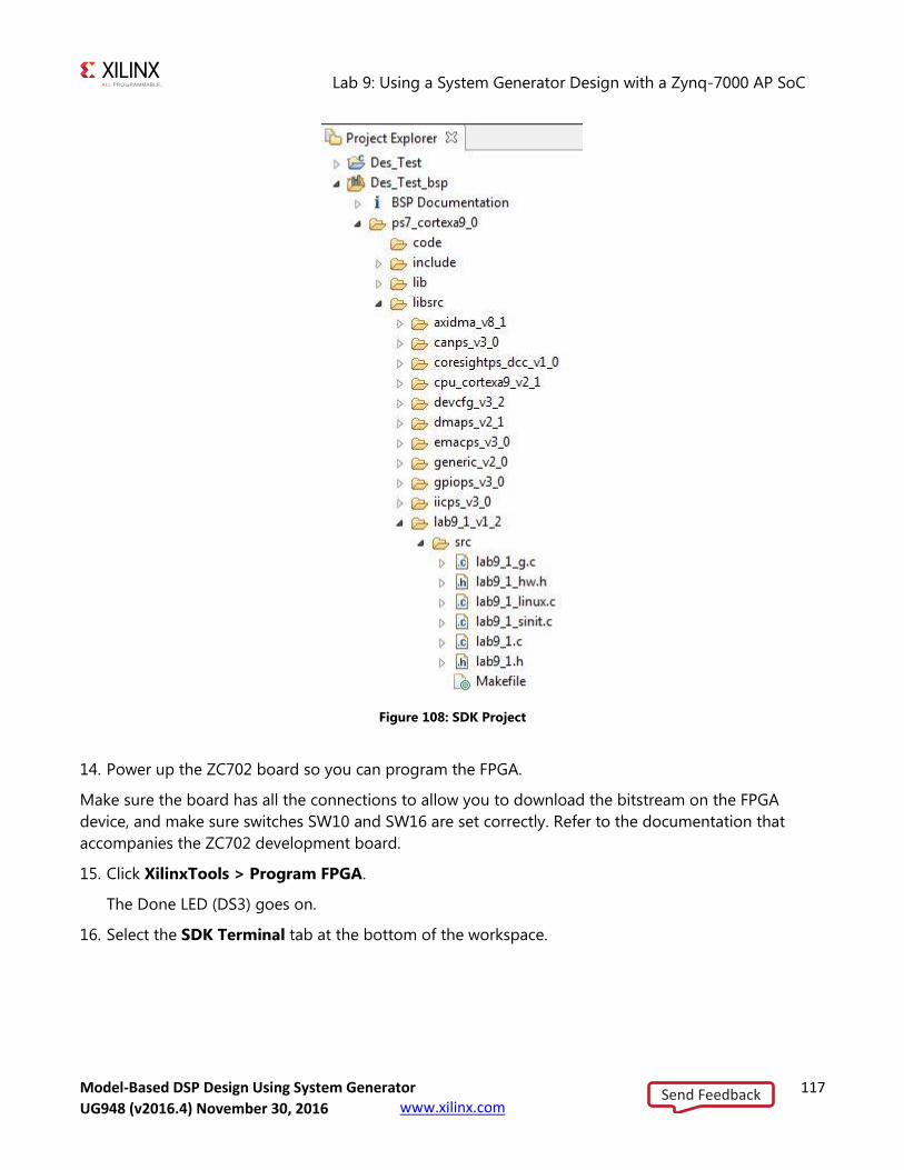
Lab 9: Using a System Generator Design with a Zynq-7000 AP SoC
Model-Based DSP Design Using System Generator 117 UG948 (v2016.3) October 28, 2016 www.xilinx.com
Figure 108: SDK Project
14. Power up the ZC702 board so you can program the FPGA.
Make sure the board has all the connections to allow you to download the bitstream on the FPGA
device, and make sure switches SW10 and SW16 are set correctly. Refer to the documentation that
accompanies the ZC702 development board.
15. Click XilinxTools > Program FPGA.
The Done LED (DS3) goes on.
16. Select the SDK Terminal tab at the bottom of the workspace.
Send FeedbackUG948 (v2016.4) November 30, 2016

Lab 9: Using a System Generator Design with a Zynq-7000 AP SoC
Model-Based DSP Design Using System Generator 118 UG948 (v2016.3) October 28, 2016 www.xilinx.com
17. To set up the terminal in the SDK Terminal tab, click the Connect icon and perform the following:
a. Select Connection Type > Serial.
b. Select the COM port to which the USB UART cable is connected. On Windows, if you are not
sure, open the Device Manager and identify the port with the Silicon Labs driver under Ports
(COM & LPT).
c. Change the Baud Rate to 115200.
d. Click OK to exit the Terminal Settings dialog box.
e. Check that terminal is connected by message in tab title bar.
18. Right-click application project Des_Test in the Project Explorer pane.
a. Select Run As > Launch on Hardware.
19. Switch to the SDK Terminal tab and confirm that Hello World was received.
20. Expand the container Des_Test and then expand the container src.
21. Double-click the helloworld.c file.
22. Replace the contents of this file with the contents of the file hello_world_final.c from the lab9
directory.
23. Save the helloworld.c source code.
24. Right-click application project Des_Test in the Explorer pane, and select Run As > Launch on
Hardware.
Note: If a window opens containing the text “debug session already exists”, click OK in that
window.
25. Review the results in the SDK Terminal tab (shown below).
Send FeedbackUG948 (v2016.4) November 30, 2016
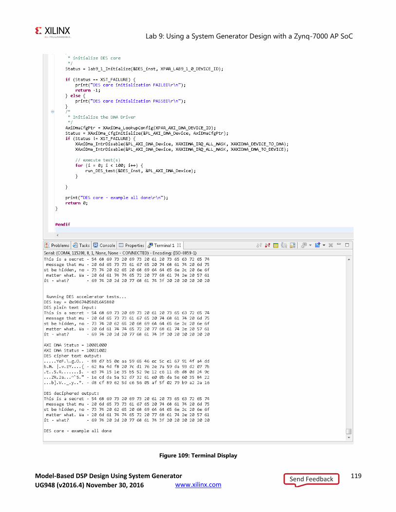
Lab 9: Using a System Generator Design with a Zynq-7000 AP SoC
Model-Based DSP Design Using System Generator 119 UG948 (v2016.3) October 28, 2016 www.xilinx.com
Figure 109: Terminal Display
Send FeedbackUG948 (v2016.4) November 30, 2016
Lab 9: Using a System Generator Design with a Zynq-7000 AP SoC
Model-Based DSP Design Using System Generator 120 UG948 (v2016.3) October 28, 2016 www.xilinx.com
Summary In this lab, you learned how to export your Vivado design containing System Generator IP to the SDK
software environment and integrate the driver files automatically created by System Generator to run
the application on the ZC702 board. You then viewed the result of the acceleration.
The following solutions directory contains the final System Generator (*.slx) files for this lab. The
solutions directory does not contain the IP output from System Generator, the files and directories
generated when Vivado is executed, or the SDK workspace.
C:/SysGen_Tutorial/Lab9/solution
Send FeedbackUG948 (v2016.4) November 30, 2016

Model-Based DSP Design Using System Generator 121 UG948 (v2016.3) October 28, 2016 www.xilinx.com
Legal Notices
Please Read: Important Legal Notices The information disclosed to you hereunder (the "Materials") is provided solely for the selection and use of Xilinx products. To the maximum
extent permitted by applicable law: (1) Materials are made available "AS IS" and with all faults, Xilinx hereby DISCLAIMS ALL WARRANTIES
AND CONDITIONS, EXPRESS, IMPLIED, OR STATUTORY, INCLUDING BUT NOT LIMITED TO WARRANTIES OF MERCHANTABILITY,
NON-INFRINGEMENT, OR FITNESS FOR ANY PARTICULAR PURPOSE; and (2) Xilinx shall not be liable (whether in contract or tort,
including negligence, or under any other theory of liability) for any loss or damage of any kind or nature related to, arising under, or in
connection with, the Materials (including your use of the Materials), including for any direct, indirect, special, incidental, or consequential loss
or damage (including loss of data, profits, goodwill, or any type of loss or damage suffered as a result of any action brought by a third party)
even if such damage or loss was reasonably foreseeable or Xilinx had been advised of the possibility of the same. Xilinx assumes no
obligation to correct any errors contained in the Materials or to notify you of updates to the Materials or to product specifications. You may not
reproduce, modify, distribute, or publicly display the Materials without prior written consent. Certain products are subject to the terms and
conditions of the Limited Warranties which can be viewed at http://www.xilinx.com/warranty.htm; IP cores may be subject to warranty
and support terms contained in a license issued to you by Xilinx. Xilinx products are not designed or intended to be fail-safe or for use in any
application requiring fail-safe performance; you assume sole risk and liability for use of Xilinx products in Critical Applications:
http://www.xilinx.com/warranty.htm#critapps.
AUTOMOTIVE APPLICATIONS DISCLAIMER
AUTOMOTIVE PRODUCTS (IDENTIFIED AS “XA” IN THE PART NUMBER) ARE NOT WARRANTED FOR USE IN THE DEPLOYMENT OF
AIRBAGS OR FOR USE IN APPLICATIONS THAT AFFECT CONTROL OF A VEHICLE (“SAFETY APPLICATION”) UNLESS THERE IS A
SAFETY CONCEPT OR REDUNDANCY FEATURE CONSISTENT WITH THE ISO 26262 AUTOMOTIVE SAFETY STANDARD (“SAFETY
DESIGN”). CUSTOMER SHALL, PRIOR TO USING OR DISTRIBUTING ANY SYSTEMS THAT INCORPORATE PRODUCTS,
THOROUGHLY TEST SUCH SYSTEMS FOR SAFETY PURPOSES. USE OF PRODUCTS IN A SAFETY APPLICATION WITHOUT A
SAFETY DESIGN IS FULLY AT THE RISK OF CUSTOMER, SUBJECT ONLY TO APPLICABLE LAWS AND REGULATIONS GOVERNING
LIMITATIONS ON PRODUCT LIABILITY.
©Copyright 2013-2016 Xilinx, Inc. Xilinx, the Xilinx logo, Artix, ISE, Kintex, Spartan, Virtex, Zynq, UltraScale and other designated brands
included herein are trademarks of Xilinx in the United States and other countries. All other trademarks are the property of their respective
owners.
Send FeedbackUG948 (v2016.4) November 30, 2016