vlsi_cadence_synopsis.pdf gv
DESCRIPTION
jghjhTRANSCRIPT
Crafting a ChipA Practical Guide to the
UofU VLSI CAD Flow
Erik BrunvandSchool of Computing
University of Utah
August 24, 2006

Draft August 24, 2006
2
Contents
1 Introduction 9
1.1 Cad Tool Flows . . . . . . . . . . . . . . . . . . . . . . . . 10
2 Cadence ICFB 15
2.1 Cadence Design Framework . . . . . . . . . . . . . . . . . 15
2.2 Starting Cadence . . . . . . . . . . . . . . . . . . . . . . . 17
3 Composer Schematic Capture 23
3.1 Starting Cadence and Making a new Working Library . . . . 24
3.2 Creating a New Cell . . . . . . . . . . . . . . . . . . . . . . 25
3.3 Schematics that use Transistors . . . . . . . . . . . . . . . . 35
3.4 Printing Schematics . . . . . . . . . . . . . . . . . . . . . . 38
3.4.1 Modifying Postscript Plot Files . . . . . . . . . . . 42
3.5 Variable, Pin, and Cell Naming Restrictions . . . . . . . . . 43
4 Verilog Simulation 45
4.1 Verilog Simulation of Composer Schematics . . . . . . . . . 48
4.1.1 Verilog-XL: Simulating a Schematic . . . . . . . . 49
4.1.2 NC Verilog: Simulating a Schematic . . . . . . . . 67
4.2 Behavioral Verilog Code inComposer . . . . . . . . . . . 75
4.2.1 Generating a Behavioral View . . . . . . . . . . . . 75
4.2.2 Simulating a Behavioral View . . . . . . . . . . . . 78
4.3 Stand-Alone Verilog Simulation . . . . . . . . . . . . . . . 79
4.3.1 Verilog-XL . . . . . . . . . . . . . . . . . . . . . . 80
CONTENTS Draft August 24, 2006
4.3.2 NC Verilog . . . . . . . . . . . . . . . . . . . . . 86
4.3.3 vcs . . . . . . . . . . . . . . . . . . . . . . . . . . 91
4.4 Timing in Verilog Simulations . . . . . . . . . . . . . . . . 98
4.4.1 Behavioral versus Transistor Switch Simulation . . . 98
4.4.2 Behavioral Gate Timing . . . . . . . . . . . . . . . 101
4.4.3 Standard Delay Format (SDF) Timing . . . . . . . . 104
4.4.4 Transistor Timing . . . . . . . . . . . . . . . . . . . 106
5 Virtuoso Layout Editor 113
5.1 An Inverter Schematic . . . . . . . . . . . . . . . . . . . . 113
5.2 Layout for an Inverter . . . . . . . . . . . . . . . . . . . . . 116
5.2.1 Virtuoso Command Overview . . . . . . . . . . . 132
5.3 Printing Layouts . . . . . . . . . . . . . . . . . . . . . . . . 135
5.4 Design Rule Checking . . . . . . . . . . . . . . . . . . . . 135
5.4.1 DIVA Design Rule Checking . . . . . . . . . . . . 137
5.5 Generating an Extracted View . . . . . . . . . . . . . . . . 141
5.6 Layout Versus Schematic Checking . . . . . . . . . . . . . 141
5.6.1 Generating ananalog-extractedview . . . . . . . . 152
5.6.2 Overall Cell Design Flow (so far...) . . . . . . . . . 152
5.7 Standard Cell Template . . . . . . . . . . . . . . . . . . . . 152
5.7.1 Standard Cell Geometry Specification . . . . . . . . 154
5.7.2 Standard Cell I/O Pin Placement . . . . . . . . . . . 159
5.7.3 Standard Cell Transistor Sizing . . . . . . . . . . . 160
6 Spectre Analog Simulator 165
6.1 Simulating a Schematic . . . . . . . . . . . . . . . . . . . . 167
6.1.1 Simulation with the Spectre Analog Environment . . 171
6.2 Simulating with a Config View . . . . . . . . . . . . . . . . 176
6.3 Mixed Analog/Digital Simulation . . . . . . . . . . . . . . 179
6.3.1 Final Words about Mixed Mode Simulation . . . . . 193
6.4 DC Simulation . . . . . . . . . . . . . . . . . . . . . . . . 195
4
Draft August 24, 2006 CONTENTS
6.4.1 Parametric Simulation . . . . . . . . . . . . . . . . 197
7 Cell Characterization 203
7.1 Characterization with Spectre . . . . . . . . . . . . . . . . . 203
7.2 Characterization with SignalStorm . . . . . . . . . . . . . . 203
7.3 Liberty (.lib) file format . . . . . . . . . . . . . . . . . . . . 203
8 Verilog Synthesis 205
8.1 Synopsys Synthesis: dcshell . . . . . . . . . . . . . . . . . 205
8.2 Synopsys Module Compiler . . . . . . . . . . . . . . . . . 205
8.3 Cadence BuildGates . . . . . . . . . . . . . . . . . . . . . . 205
8.4 Cadence to Synopsys (CSI) Interface . . . . . . . . . . . . . 206
9 Abstract Generation 207
9.1 Abstract Tool . . . . . . . . . . . . . . . . . . . . . . . . . 207
9.2 LEF File Generation . . . . . . . . . . . . . . . . . . . . . 207
10 SOC Encounter Place and Route 209
10.1 Encounter GUI . . . . . . . . . . . . . . . . . . . . . . . . 209
10.2 Encounter Scripting . . . . . . . . . . . . . . . . . . . . . . 209
11 Chip Assembly 211
11.1 Importing the Design to DFII . . . . . . . . . . . . . . . . . 211
11.2 Pad Frames in Encounter . . . . . . . . . . . . . . . . . . . 211
11.3 Pad Frames in CCAR . . . . . . . . . . . . . . . . . . . . . 211
11.4 Final GDS Generation . . . . . . . . . . . . . . . . . . . . 211
12 Design Example: TinyMIPS 213
12.1 MIPS: Synthesis . . . . . . . . . . . . . . . . . . . . . . . . 213
12.2 MIPS: Place and Route . . . . . . . . . . . . . . . . . . . . 213
12.3 MIPS: Simulation . . . . . . . . . . . . . . . . . . . . . . . 213
12.4 MIPS: Final Assembly . . . . . . . . . . . . . . . . . . . . 213
5
CONTENTS Draft August 24, 2006
A Tool Administration 215
A.1 Installing Cadence Tools . . . . . . . . . . . . . . . . . . . 215
A.2 Installing the NCSU CDK . . . . . . . . . . . . . . . . . . 215
A.3 Installing Synopsys Tools . . . . . . . . . . . . . . . . . . . 215
B Highlights of the Tools 217
B.1 ICFB . . . . . . . . . . . . . . . . . . . . . . . . . . . . . 218
B.2 Composer Schematics . . . . . . . . . . . . . . . . . . . . . 218
B.3 Verilog Simulation . . . . . . . . . . . . . . . . . . . . . . 218
B.4 Spectre Analog Simulation . . . . . . . . . . . . . . . . . . 218
B.5 Virtuoso Layout . . . . . . . . . . . . . . . . . . . . . . . . 218
B.6 Abstract Generation . . . . . . . . . . . . . . . . . . . . . . 218
B.7 SignalStorm Library Characterization . . . . . . . . . . . . 218
B.8 SOC Encounter . . . . . . . . . . . . . . . . . . . . . . . . 218
B.9 Synopsys Synthesis . . . . . . . . . . . . . . . . . . . . . . 218
B.10 ICC Chip Assembly Router . . . . . . . . . . . . . . . . . . 218
C Tool and Setup Scripts 219
C.1 Cadence Setup Scripts . . . . . . . . . . . . . . . . . . . . 219
C.2 Synopsys Setup Scripts . . . . . . . . . . . . . . . . . . . . 219
C.3 TCL script basics . . . . . . . . . . . . . . . . . . . . . . . 219
C.4 Cadence Tool Scripts . . . . . . . . . . . . . . . . . . . . . 219
C.4.1 SOC Encounter . . . . . . . . . . . . . . . . . . . . 219
C.4.2 BuildGates Synthesis . . . . . . . . . . . . . . . . . 219
C.5 Synopsys Tool Scripts . . . . . . . . . . . . . . . . . . . . . 219
C.5.1 dcshell Synthesis . . . . . . . . . . . . . . . . . . 219
C.5.2 Module Compiler Synthesis . . . . . . . . . . . . . 219
C.5.3 PrimeTime Timing Analysis . . . . . . . . . . . . . 219
D MOSIS SCMOS rev8 Design Rules 221
6
Draft August 24, 2006 CONTENTS
E Technology and Cell Libraries 223
E.1 NCSU CDK . . . . . . . . . . . . . . . . . . . . . . . . . . 223
E.1.1 UofU Extensions . . . . . . . . . . . . . . . . . . . 223
E.2 Standard Cell Libraries . . . . . . . . . . . . . . . . . . . . 223
E.2.1 UofUDigital . . . . . . . . . . . . . . . . . . . . . 223
E.2.2 UofUAsync . . . . . . . . . . . . . . . . . . . . . 223
E.2.3 OSU Libraries . . . . . . . . . . . . . . . . . . . . 223
Bibliography 224
Index 226
7

CONTENTS Draft August 24, 2006
8
Chapter 1
Introduction
THE DESIGN process for digital integrated circuits is extremely com-plex. Unfortunately, the Electronic Design Automation (EDA) andComputed Aided Design (CAD) tools that are essential to this de-In this book I’ll call the
tools “CAD tools” andthe companies “EDAcompanies”
sign process are also extremely complex. Finding a combination of toolsand a way of using those tools that works for a particular design is knowas finding a “tool path” for that project. This book will introduce one paththrough these complex tools that can be used to design digital integratedcircuits. The tool path described in this book uses tools from Cadence(www.cadence.com) and Synopsys (www.synopsys.com) that are availableto university students through special arrangements that these companiesmake with universities. Tool bundles that would normally cost hundreds ofthousands or even millions of dollars if purchased directly from the compa-nies are made available through “university programs” at small fixed fees.
In order to justify these small fees, however, the EDA companies typ-ically reduce their costs by offering very limited support for these tools touniversity customers. In an industrial setting there would likely be an en-tire CAD support department whose job it is to get the tools running and todevelop tool flows for projects within the company. Few universities, how-ever, can afford that type of support for their CAD tools. That leavesInstructions for
installing the CAD toolscan be found in theappendices
universities to sink or swim with these complex tools making it all the moreimportant to find a usable tool path through the confusing labyrinth of thetool suites. This book is an attempt to codify at least one working tool pathfor a Cadence/Synopsys flow that students and researchers can use to de-sign digital integrated circuits. It includes tutorials for specific tools, and anextended example of how these tools are used together to design a simpleintegrated circuit.
In addition to the CAD tools from Cadence and Synopsys, The tutori-als assume that you have some sort of CMOS standard cell library avail-
CHAPTER 1: Introduction Draft August 24, 2006
able. The specific examples in this book will use a cell library developedat the University of Utah specifically for our VLSI classes known as theUofU Digital library. This library, and the technology information avail-Details about these
libraries can also befound in the appendices
able through the NCSU CDK (North Carolina State University Cadence De-sign Kit), are freely available from the University of Utah and North Car-olina State University respectively. If you don’t have these libraries youshould be able to follow most of the tutorials with your own library, but youmust have a library of some sort.
1.1 Cad Tool Flows
The general tool flow described here uses CMOS standard cells with auto-matic place and route to design the chip, but also includes details of howCAD tools typically do
not include anytechnology or cell data.
This data comes directlyfrom the chip and cellvendors and contains
information specific totheir technologies.
to design custom cells as layout and add those cells to a library. This cus-tom portion of the flow could, of course, be used to design a fully customchip. It can also be used to design your own cell library. Designing a celllibrary involved not only designing the individual cells, but characterizingthose cells in terms of their delay in the face of different output loads andinput slopes, and codifying that behavior in a way that the synthesis toolscan use. The cells also must have their physical parameters characterizedso that the place and route tools have enough information to assemble theminto a chip. Finally, simulation at a variety of levels of detail and timingaccuracy is essential if a functional chip is to result from this process.
This entire tool flow will use a large number of tools from both Cadenceand Synopsys, a large number of different file formats and conversion pro-grams, and a lot of different ways of thinking about circuits and systems.File types for the
complete flow aredescribed as they areused in the flow and
documented in theappendices. In addition
to Cadence databasefiles, they include .lib,
.db, .lef, .gds, .sdf, .def,.v, .sdc, and .tcl files.
This is inevitable in a task as complex as designing a large integrated cir-cuit, but it can be intimidating. One ramification of the type of complexityinherent in VLSI design is that the tools, designed as they are to handlevery large collections of cells and transistors, aren’t much simpler to use onjust 4 transistors than they are on 4,000, 400,000, or 4,000,000 transistordesigns. It is not easy to simply start small and add features. One must,in some ways, do it all right from the start which makes the learning curvequite steep. There are lots of pieces of the flow that must be available rightfrom the start which can be overwhelming at first. Hopefully by breakingthe tool flow into individual tool tutorials, and with detailed walk-throughtutorials with lots of screen shots of what you should see on the screen, thiscan be made less intimidating.
Of course, as with any tool with a steep learning curve, once you’vemade it up the steep part of the curve, you may not want to refer back tothe level of detail contained in the tutorial descriptions. For that stage ofthe process I’ve included slimmed down “highlights” versions of the tool
10
Draft August 24, 2006 1.1: Cad Tool Flows
instructions in the appendices of this volume. If you need to refer back to atool that you’ve used before but haven’t used for a while, you may just needto glance at the highlights in the appendices rather than walk through theentire tutorial again.
I need at least one figure of the whole tool flow here, and perhaps in-dividual pictures of flows for different purposes. For example, a flow forcell design, a flow for standard cell from Verilog descriptions, and a generalflow.
Custom VLSI and Cell Design Flow
This is a tool flow for designing custom VLSI systems where the designgoes down to the circuit fabrication layout. This flow starts with transis-tor schematics at the front end and uses custom layout to design portionsof the system. It is used for designing cell librarys as well as for design-ing performance-critical portions of larger circuits where individual designof the transistor-level circuits is desired. The front end for this flow istransistor-level schematics inComposer. These schematics may be sim-ulated at a functional level using Verilog simulators likeVerilog-XL andNC Verilog, and with a detailed analog simulator likeSpectre. The backend is composite layout usingVirtuoso and more detailed simulation usinganalog simulators.
If the final target is a cell library then the cells can be characterized forperformance using a simulator likeSpectre or by using a library character-izer tool like Signalstorm. These chacterizations are required if you wouldlike to use these cells with a synthesis system later on. Abstract view canalso be generated so that the cells can be used with a place and route system.
ASIC and Standard Cell Design Flow
THis is a tool flow for system level design using a CMOS standard celllibrary. The library may be a commercial library or it may be one thatyou design yourself, or a combination of the two. The front end can beschematics designed using cells from these libraries, or Verilog code. If thesystem decription is in structural Verilog code which is set of instantiationsof standard cells in Verilog, then this can be used directly as the front-enddescription. If the Verilog is behavioral Verilog, then a synthesis step us-ing Synopsysdc shell, design vision or module compiler, or CadenceBuildGates can synthesize the behavioral description into a Verilog struc-tural description.
These descriptions, whether structural, behavioral, or a combination of
11
CHAPTER 1: Introduction Draft August 24, 2006
both, can be simulated for functionality usingVerilog-XL or NC Verilog.These simulations may use a zero-delay, unit-delay, or extracted delay model.The extracted delays come from the synthesis systems which extract timingsbased on the cell characterizations.
The back end to the ASIC flow usesSOC Encounter to place and routethe structural file into a full chip. This description may be extracted again toget timings that include wiring delays, or the timing can be analyzed usinga static timing analyzer like SynopsysPrimeTime. The system can also besimulated in mixed-timing mode where parts of the circuit are simulated at aswitch level using a Verilog simulator and parts of the circuit are simulatedat a detailed level using an analog simulator likeSpectre. The final resultis a gds (also known as stream) file that can be sent to a fabrication servicesuch as MOSIS to have the chips built.
Of course, the tool flows described here only scratches the surface ofwhat the tools can do! Please feel free to explore, press on likely lookingbuttons, and read the manuals to explore the tools further. If you discovernew and wonderful things that the tools can do, document those additionsto the flow and let me know and I’ll include them in subsequent releases ofthis manual.
What this Manual is and isn’t
This manual includes walk-through tutorials for a number of tools from Ca-dence and Synopsys, and description of how to combine those tools into aworking tool flow for VLSI design. It isnot a manual on the VLSI designprocess itself! There are many fine textbooks about VLSI design available.This is a “lab manual” that is meant to go along with those textbooks anddescribe the nuts and bolts of working with the CAD tools. I will assumethat you either already understand general VLSI design, or are learning thatas you proceed through the tutorials contained in this manual.
Bugs in the Tools?
Before we dive into the tutorials, here’s a quick word about tool bugs. Thesetools are complex, but so are the systems that you can design with them.They also feel very cumbersome and buggy at times, and at times they are!However, even with the inevitable bugs that creep into tools like this, I en-courage you to follow the tutorials carefully and resist the temptation toblame a tool bug each time you run into a problem! I’ve found in teachingcourses with these tools for years that it is almost 100% certaintly that ifyou’re having trouble with a tool in a class setting, that it’s something thatyou’ve done or some quirk of your data rather than a bug in the tool. It’s
12
Draft August 24, 2006 1.1: Cad Tool Flows
amazing how subtle (or sometimes how obvious!) the differences can bein what you’re doing and what the procedure specifies. Relax, take a deepbreath, and think carefully about what’s going on and what might cause it.Read the error messages carefully. Occasionally there is real informationin the error message! Try explaining things to a fellow student. Often inthe process of explaining what you’re doing you’ll see what’s going on. Letsomeone else look at it. Let your first instinct be to try to figure out what’sgoing on, not to blame the tool! If the tool turns out the be the problem,at least you will have exhausted the more likely causes of the problem firstbefore you discover this.
Typographical Conventions
Finally, a word about typographical conventions. I will try to stick to these,but don’t promise perfect adherence to these conventions! In general:
• I’ll try to use boxed, fixed width font for any text thatyou should type in to the system. This, hopefully, will look a little likethe fixed-width font you’ll see on your screen while you’re typing. Soif you are supposed to type in a command likecad-ncsu it willlook like that.
• I’ll try to use bold face for things that you should see on the sceenor in windows that the tools pop up. So if you should seeCreateLibrary in the title bar of the window, it will look like that in the text.
• I’ll use slanted text in the marginal notes. These are little points ofinterest that are ancillary or parenthetical to the main text. This is a margin note
• I’ll use a non-serifed face to give the names of the tools that we’reworking with. Note that the name of the tool, likeComposer,is seldom the name of the executable program that you run to getto that program. For those, refer back to the typed commands likecad-ncsu .
13

CHAPTER 1: Introduction Draft August 24, 2006
14
Chapter 2
Cadence ICFB
CADENCE is a large company that offers a dizzying array of softwarefor Electronic Design Automation (EDA) or Computer Aided De-sign (CAD) applications. Cadence CAD software is generallyThe custom design
tutorials are a goodstarting point for customanalog IC design too
targeted at the design of electrical circuits, both digital and analog, andextending from extremely low-level VLSI design to the design of circuitboards for large systems. This book is primarily interested in digital inte-grated circuit (IC) design so we’ll look primarily at those tools from theCadence suite.
2.1 Cadence Design Framework
Many of the digital IC design tools from Cadence are grouped under aframework calledDesign Framework II ( dfII). The dfII environment in-tegrates a variety of design activities including schematic capture (Com-poser), simulation (Verilog-XL or NC Verilog), layout design (Virtuosoand Virtuoso-XL, design rule checking (DRC) (Diva and Assura), layoutversus schematic checking (LVS) (Diva and Assura), and abstract gen-eration for standard cell generation (Abstract). These are all individualprograms that perform a piece of the digital IC design process, but are allaccessible (to a greater or lesser extent) through thedfII framework andthe dfII user interface. Note that many of these programs were developedby separate companies that have been acquired by Cadence and folded intothe dfII framework after that acquisition. Thus, some integrate better thanothers!
As we’ll see, though, there are some pieces of the Cadence tool flowthat are not linked into thedfII framework. Most notably place and route ofstandard cells withSOC Encounter, connection of large blocks withICCChip Assembly Router (CAR) and Verilog synthesis withBuildGates
CHAPTER 2: Cadence ICFB Draft August 24, 2006
are done in separate programs with separate interfaces.
However, we’ll start with thedfII tools in this tool flow, so we’ll needto start up thedfII framework. The executable in the Cadence tool suite thatstarts up this framework is calledicfb which stands for Integrated CircuitFront to Back design. If you were to set up your search path so that theCadence tools were on your path, and execute theicfb command youwould see thedfII framework start up.
Unfortunately, this wouldn’t help you much! It turns out that having thetool framework is only half the battle. You also need detailed technologyinformation about the devices you want to use for your design. This detaileddesign information includes technology information about the IC processthat you are using and libraries of transistors, gates, or larger modules thatyou can use to build your circuits. This information includes many files ofdetailed (and somewhat inscrutable) information, and does not come fromCadence. Instead, it comes from the vendor of the IC process and from thevendor of the gate and module cells that you are using in your design. Thiscollection design information is typically called a “Cadence Design Kit” orCDK.
For this book we will use technology information for IC processes sup-ported by the MOSIS chip fabrication service. This information has beenassembled into a CDK by the good folks at North Carolina State University(NCSU). The NCSU CDK has detailed techology information for all theWe’re using
NCSU CDK v1.5 processes currently offered through MOSIS. These processes are availableeither in “vendor” rules which have have the actual specifics of the technol-ogy as offered by the vendor, or through abstracted rules known as ScalableCMOS or SCMOS rules. The SCMOS are scalable in the sense that a de-sign done in the SCMOS rules should, theoretically, be useable in any of theMOSIS processes simply by changing a scalaing parameter. That means thatthe SCMOS rules are a little conservative compared to some of the vendorrules because they have to work for all the different vendors.
Of course, it’s not quite that simple because as design features get smallerand smaller the IC structures don’t scale at the same rate. But, it workspretty well. To handle the differences required by smaller geometry pro-cesses MOSIS has a number of modifiers to the SCMOS rules (SCMOSfor “generic” SCMOS, SCMOSSUBM for submicron processes, and SC-MOS DEEP for even smaller processes). For this class we’ll be using theWe’re using the
SCMOS V8.0 rules. SCMOSSUBM rules which will then be fabricated on the AMI C5N 0.5µCMOS process.
But, that’s getting ahead of ourselves a little bit. The important thing fornow is that without the NCSU CDK, we won’t have any technology infor-mation to work with. So, instead of starting upicfb directly, we’ll start it upwith the NCSU CDK already loaded. This will happen by calling Cadence
16
Draft August 24, 2006 2.2: Starting Cadence
from a script that we’ve written instead of calling the tool directly. Thisscript will start a new shell, set a bunch of required environment variables,and call the icfb tool with the right switches set. Other tools for the rest ofthis book will use similar scripts.
2.2 Starting Cadence
Before you start using cadence you need to complete the following steps:
First make a directory from which to run Cadence. This is important sothat all of Cadence’s files end up in a consistent location. It’s also nice tohave all of Cadence’s setup and data files in a subdirectory and not cloggingup your home directory. I recommend making an ICCAD directory and CAD tools can generate
a lot of temporary andauxiliary files!
then under that making a cadence directory. Later on we’ll add to that bymaking separate directories for the other IC tools like Synopsys dcshell,module complier, SOC Encounter and so on under that ICCAD directory.
cdmkdir IC CADmkdir IC CAD/cadence
Now it’s handy to set a few environment variables. In particular youwant to set your UNIX search path to include the directory that has thestartup scripts for the CAD tools. You also need to set an environment vari-able that points to a location for class-specific modifications to the generalCadence configuration files. I recommend that you put these commands inyour .cshrc or .tcshrc file so you won’t have to retype them each time youstart a shell. If you’re using bash you’ll have to adjust the syntax slightly,and if you’re not at the University of Utah these paths will be different.
set path = ($path /uusoc/facility/cadcommon/local/bin/F06)setenv LOCALCADSETUP /uusoc/facility/cadcommon/local/class/6710
By default the tool scripts will start the tool in the directory that youare connected to when you execute the script. If you’d like to haveAll the Cadence and
Synopsys CAD tools runon Solaris or Linux so ifyou don’t have a goodgrasp of basic UNIXcommands, now’s thetime to go learn them!
Cadence connect to a specific directory automatcally every time you executethe script you can set your CADENCEDIR environment variable. This wayyou don’t have to remember to connect to your $HOME/ICCAD/cadencedirectory each time (but it means you can’t have different directories fordifferent projects without unsetting that environment variable):
setenv CADENCEDIR $HOME/ICCAD/cadence
Finally, you need to copy one Cadence init file from the NCSU CSKdirectory so that things get initialized correctly. The file is called .cdsinit
17
CHAPTER 2: Cadence ICFB Draft August 24, 2006
(note the initial dot!). You can put it in your $HOME directory so thatyou’ll always get that init file, or you can put it in the directory from whichyou start Cadence if you think you might ever want to start Cadence froma different directory for different projects or classes with a different .cdsinitfile.
I recommend making this a symbolic link so that if the system-wide.cdsinit file is updated you’ll see the new version automatically. Again, ifyou’re not at the University of Utah these paths will be different.
l n -s /uusoc/facility/cadcommon/NCSU/CDK-F06/.cdsinit $HOMEorcd $HOME/ICCAD/cadenceln -s /uusoc/facility/cadcommon/NCSU/CDK-F06/.cdsinit .
Now that you have your own cadence directory (called$HOME/IC CAD/cadence if you’ve followed the directions up to this point),set your path, and linked the NCSU .cdsinit file either to $HOME or to$HOME/IC CAD/cadence you’re ready to start Cadenceicfb with the NCSUCDK. If you’ve set your environment variable CADENCEDIR then the classscripts will also connect you to the right working directory each time youstart the tools. If not, please connect to your $HOME/ICCAD/cadence di-rectory (or where ever you wish to start Cadence from) first.
Start Cadence with the command:
cad-ncsu
Of course, once you set this all up once, you should be able to jumpWe’re using dfII fromthe IC v5.1.41 release right to the cad-ncsu step the next time you want to start Cadence.
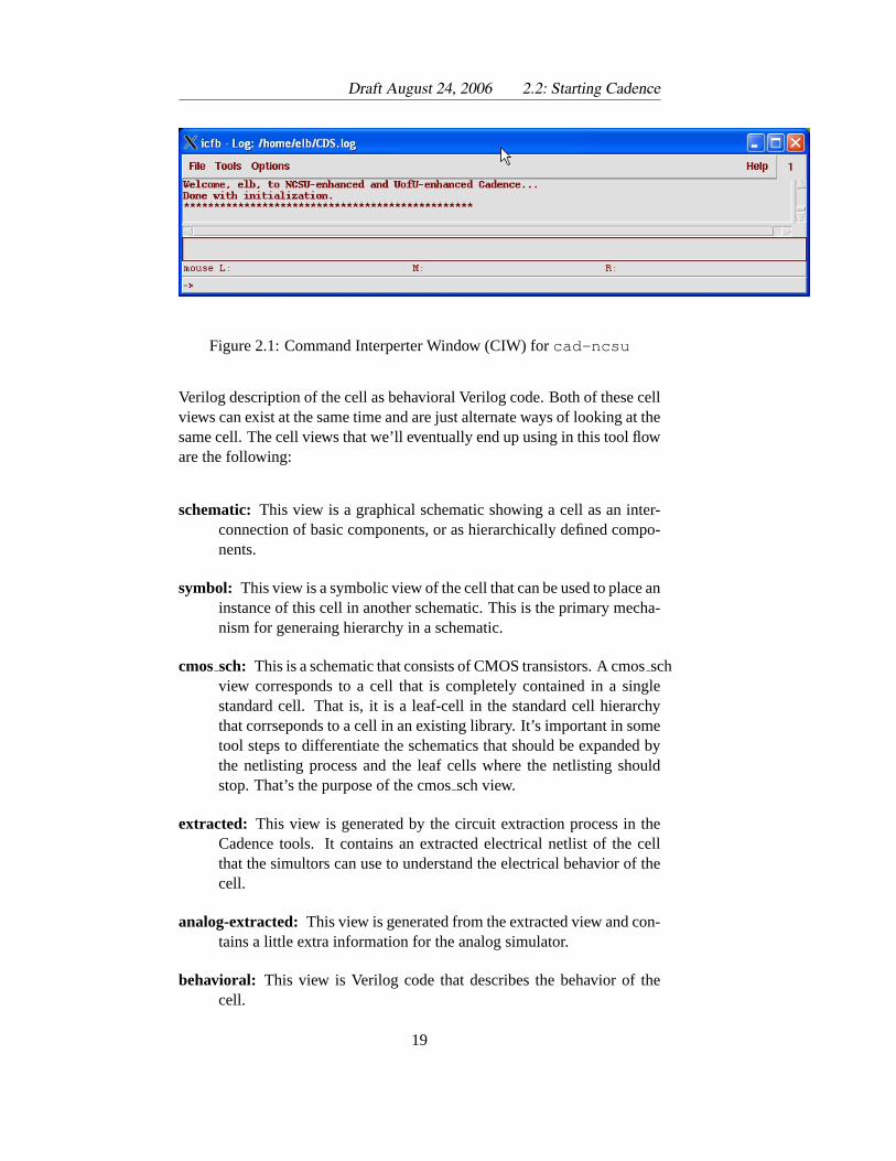
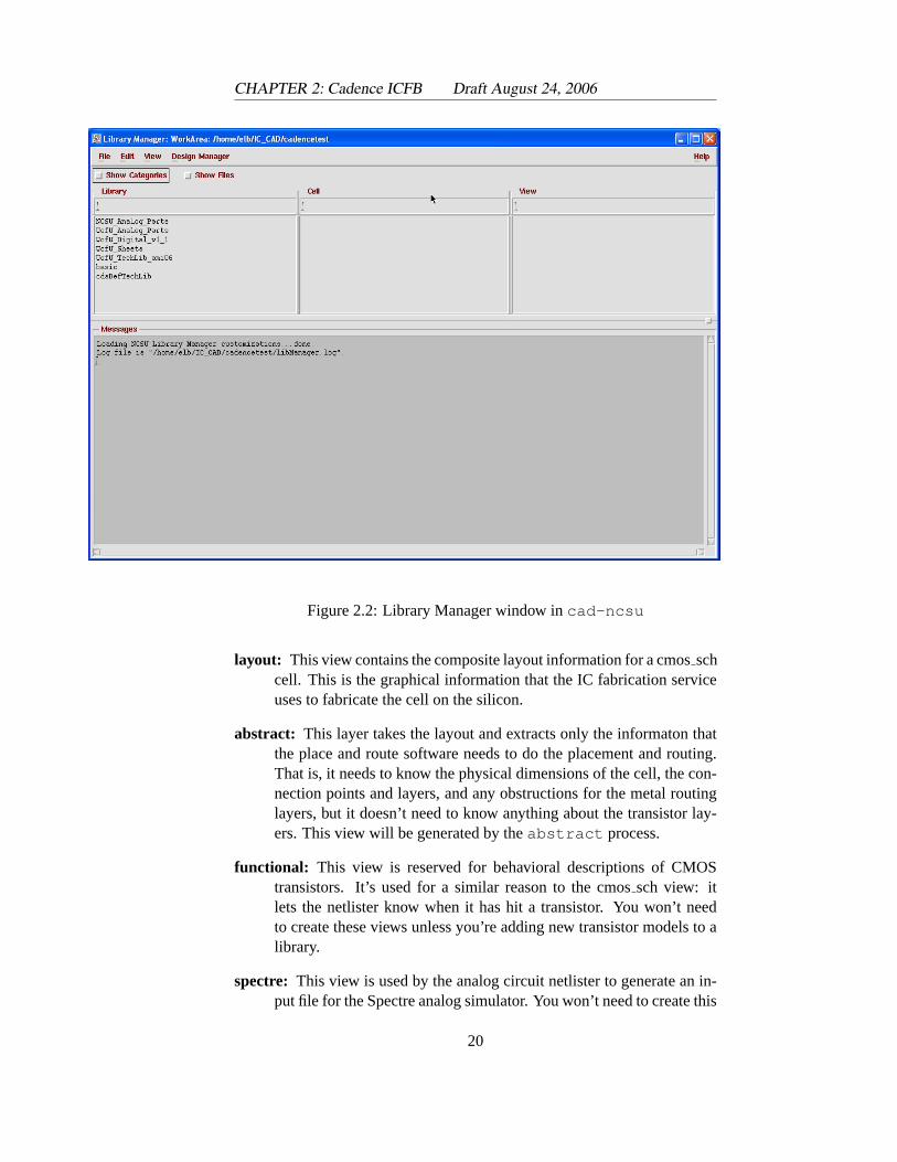
You should see two windows once things get started up. The first isthe Command Interperter Window or CIW. It’s shown in Figure 2.1. Theother is theLibrary Manager shown in Figure 2.2. The CIW is the maincommand interface for all thedfII tools. In practice you will probably nottype commands into this window. Instead you’ll use interfaces in each of thetools themselves. However, because most of the tools put their dignosticCadence also keeps the
log information in aCDS.log file which itputs in your $HOME
directory
log information into the CIW, you will refer back to it often. Also, there aresome things that just have to be done from this window. For now, just makesure that your CIW looks something like the one in Figure 2.1.
The Library Manager is a general interface to all the libraries and cellsviews that you’ll use indfII. Cells in dfII are individual circuits that youwant to design separately. IndfII there is a notion of a “cell view” whichmeans that you can look at a cell in a number of different ways (in differentviews). For example, you might have a shematic view that shows the cellin terms of its components in a graphical schematic, or you might have a
18
Draft August 24, 2006 2.2: Starting Cadence
Figure 2.1: Command Interperter Window (CIW) forcad-ncsu
Verilog description of the cell as behavioral Verilog code. Both of these cellviews can exist at the same time and are just alternate ways of looking at thesame cell. The cell views that we’ll eventually end up using in this tool floware the following:
schematic: This view is a graphical schematic showing a cell as an inter-connection of basic components, or as hierarchically defined compo-nents.
symbol: This view is a symbolic view of the cell that can be used to place aninstance of this cell in another schematic. This is the primary mecha-nism for generaing hierarchy in a schematic.
cmossch: This is a schematic that consists of CMOS transistors. A cmosschview corresponds to a cell that is completely contained in a singlestandard cell. That is, it is a leaf-cell in the standard cell hierarchythat corrseponds to a cell in an existing library. It’s important in sometool steps to differentiate the schematics that should be expanded bythe netlisting process and the leaf cells where the netlisting shouldstop. That’s the purpose of the cmossch view.
extracted: This view is generated by the circuit extraction process in theCadence tools. It contains an extracted electrical netlist of the cellthat the simultors can use to understand the electrical behavior of thecell.
analog-extracted: This view is generated from the extracted view and con-tains a little extra information for the analog simulator.
behavioral: This view is Verilog code that describes the behavior of thecell.
19
CHAPTER 2: Cadence ICFB Draft August 24, 2006
Figure 2.2: Library Manager window incad-ncsu
layout: This view contains the composite layout information for a cmosschcell. This is the graphical information that the IC fabrication serviceuses to fabricate the cell on the silicon.
abstract: This layer takes the layout and extracts only the informaton thatthe place and route software needs to do the placement and routing.That is, it needs to know the physical dimensions of the cell, the con-nection points and layers, and any obstructions for the metal routinglayers, but it doesn’t need to know anything about the transistor lay-ers. This view will be generated by theabstract process.
functional: This view is reserved for behavioral descriptions of CMOStransistors. It’s used for a similar reason to the cmossch view: itlets the netlister know when it has hit a transistor. You won’t needto create these views unless you’re adding new transistor models to alibrary.
spectre: This view is used by the analog circuit netlister to generate an in-put file for the Spectre analog simulator. You won’t need to create this
20
Draft August 24, 2006 2.2: Starting Cadence
view unless you’re adding new transistor models to a library. Thereare a number of other similar views for other simulators that you alsodon’t need to worry about.
A “library” is a collection of cells that are grouped together for somereason (being part of the same project, or part the same set of standardcells, for example). Libraries also have technology information attachedto them so that the cells in the library refer to a consistent set of technolgydata. This technology information is linked rather than copied so that whenupdates are made on the techology, all libraries with that technology at-tached will see the updates. For example, all the standard gates cells thatThe UofU Digital
library uses the v1 1syntax to indicateversion 1.1 of thelibrary. Cadence doesn’tlike dots in cell names!
you’ll be using (until you make your own!) are grouped into a library calledUofU Digital v1 1. You will create libraries for each of your designs sothat you can keep the design data separate for different projects. Think oflibrarires as directories that collect design dat together for a specific design.You could throw all your stuff into one directory, but it would be easier tofind and use if you separate different designs into different libraries.
You should see a bunch of libraries already listed in the Library Man-ager. If you scroll around you should be able to see the following:
NCSU TechLib xxx: These are technology libraries for each of the MO-SIS processes. The “xxx” will be filled in with information aboutwhich MOSIS process is being desctribed. We won’t use these di-rectly, and depending on how Cadence is set up for your class youmight not see these at all. If you’re not using the UofU packages,then you’ll probably see all of these.
NCSU Analog Parts: This library contains components (transistors, resis-tors, capacitors, etc.) that we’ll use for transistor-level design, andalso some components for circuit-level simulation using spectre (inthe Affirma analog circuit design environment). The switch-leveltransistor models in this library have zero delay for simulation.
NCSU Digital Parts: This library contains a variety of Boolean logic gatesthat you can use for gate-level design. Note that these gates donothave layout or place and route views so theycan not be used for ac-tually building chips! They will be used in this class just for the initial“learn about the schematic capture tool” assignment.
basic: This is the Cadence built-in library which you won’t use directly.
cdsDefTechLib: A generic Cadence technology that we won’t use.
UofU Analog Parts: This is a library with copies of the transistor com-ponents from theNCSU Analog Library , but these transistors have0.1ns of delay for switch level simulation.
21
CHAPTER 2: Cadence ICFB Draft August 24, 2006
UofU TechLib ami06: This is a technology library for the AMI C5N 0.5µlibrary using the SCMOSSUBM rules that we’ll use in the tutorials.It’s based on the NCSU technology library for this process, but hassome local tweaks that make it a little more friendly to this flow.
UofU Sheets: This library has graphics for schematic sheet borders.
UofU Digital v1 1: This is a library of standard cells developed at theIf you look at the cells inUofU Digital v1 1 youshould see that each ofthem has a number ofdifferent cell views as
defined previously
University of Utah for VLSI classes. It has the UofUTechLib ami06technology attached to it so it can be used with the AMI C5N 0.5µCMOS process through the SCMOSSUBM design rules from MO-SIS. This will all make more sense later. . .
Unfortunately, you’ll have to keep very careful track of when to usecomponents out of each of these libraries. Some have very specific uses.The only way to handle this is just to pay attention and keep track!
Now that you’ve started Cadence using thecad-ncsu script, we canmove on to using the individual EDA tools in thedfII suite...
22
Chapter 3
Composer Schematic Capture
COMPOSERis the schematic capture tool that is bundled with the thedfII ( Design Framework II) tool set. It is a full-featued schematiccapture tool that we’ll use for designing transistor level schemat-Although the schematic
tool is calledComposer in thedocumentation, it’scalled VirtuosoSchematic Editing inthe window title.Virtuoso is also thespecific name given tothe layout editor in dfII.They’re both part of thedfII Virtuoso tool suiteI guess.
ics for small cells, gate level schematics for larger circuits, and schematicscontaining a mix of gates and Verilog code for more complex circuits. Inthat case some of the components in the schematic will contain transistorsat the lowest level, and some will contain Verilog code. Because the simula-tors that are used in conjunction with Composer are all Verilog simulators,these mixed schematics can be simulated using the same simulators used byschematics with only gates or transistors.
I find schematics extremely useful for all levels of design. Even fordesigns that are done completely in Verilog code I find that connecting theVerilog components in a schematic often makes things easier to understandthan large pieces of code where connections are made with large argumentlists and named wires. Your mileage may vary, of course.
Composer has connections to all sorts of other tools in the dfII toolComposer is a part ofthe IC v5.1.41 toolssuite, and to other tool suites. We’ll look at all of them in future chapters.
• Composer is integrated with theVerilog-XL and NC Verilog sim- A file that captures thecomponent andconnection informationfor a circuit is called a“netlist,” and the processof generating that file iscalled “netlisting.”
ulators so that you can automatically export a schematic to a simula-tor. The Composer/Verilog integration will take your schematic andgenerate a Verilog netlist for simulation, and also build a simple test-bench wrapper as a Verilog file that you can modify with your owntesting commands. We’ll see how that works in the chapter on Verilogsimulation.
• There is also an interface that can take a schematic and convert thatschematic to the Verilog structural file for input to a tool that uses thattype of input. Synopsysdc shell for synthesis and CadenceSOC
CHAPTER 3: Composer Schematic Capture Draft August 24, 2006
Encounter for place and route are just two of the possible tools thatthe structural Verilog file can be used with. This interface is known asthe Cadence Synopsys Interface, or CSI, but it is a general wayto convert a schematic to a structural netlist.
• Composer has a connection with the CadenceVirtuoso-XL layouttool so that the designer can see the connection between the layoutand the schematic. This can be used as a guide for producing layoutbased on a schematic usingVirtuoso-XL, and is also a mechanismfor specifying the connectivity of a circuit when using theICC ChipAssembly Router to assemble large chip pieces.
• There’s also a connection theAffirma Analog Environment whichis an interface to the CadenceSpectre analog simulation tool. Us-ing this interface you can, for example, pick circuit nodes from yourschematic to be plotted in the analog simulation output file. This con-nection will also generate the requiredSpectre or Spice netlist fromyour schematic automatically.
• You can generate a schematic by hand, or you can generate a schematicautomatically from a Verilog structural netlist. For example, you cantake the output from Synopsysdc shell or Cadence BuildGatessynthesis and generate a schematic from that structural Verilog file.The generated will be a mess to look at! But, it will be very useful forusing the Cadence LVS (Layout Versus Schematic) checks using ei-ther Diva or Assura LVS. This will compare a layout to a schematicto make sure they are structurally the same.
For now, this chapter will introduceComposer by drawing schematicsfor simple circuits using standard cell gates and modules from the UofUDigitallibrary, and transistors from the NCSUAnalog Parts libraries. In order tofollow these steps you must have started up Cadenceicfb with the NCSUCDK extensions. This was explained in Chapter 2, and is done using thecad-ncsu script.
3.1 Starting Cadence and Making a new WorkingLibrary
Now that you have your own cadence directory (called/IC CAD/cadence if you’ve followed the suggestions up to this point), re-member to connect to that directory before starting up Cadence. Also makesure you have your LOCALCADSETUP environment variable set so thatyou get the class extentions to the Cadence setup.
24
Draft August 24, 2006 3.2: Creating a New Cell
1. Start up Cadence dfII by running the commandcad-ncsu . as de-scribed in Chapter 2. You may have used (and may still be using) adifferent setup for a different class, but please usecad-ncsu forthis class. You should get a window (called theCommand Informa-tion Window or CIW) similar to the one shown in Figure 2.1.
2. You should also get another window for theLibrary Manager asshown in Figure 2.2. The libraries that you’ll see in the defaultLi-brary Manager window are described in Chapter 2.
3. In order to build your own schematics, you’ll need to define yourLibrarys are defined in acds.lib file that iscreated in your cadencedirectory.
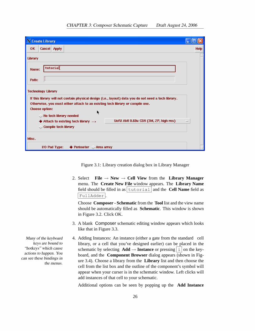
own library for your own circuits. To create a new working library inthe library manager, selectFile → New→ Library . In the CreateLibrary window that appears fill in the Name field astutorial , orwhatever you’d like to call your library. Leave thePath field blank sothat it creates the new library under the directory in which you startedCadence. If you want to create a library somewhere other than in your/IC CAD/cadence directory you can put the whole path in the pathDon’t make your library
name start with anumber, and don’t use“-“ or “.” in the name!An underscore is allright.
field. In the Technology Library box selectAttach to an existingtech library and choose theUofU AMI 0.60u C5N technology li-brary. The dialog box is shown in Figure 3.1 Now press OK and thenew library will show up in your Library Manager window.
Now the working library has been created. All the project cells (compo-nents) that you generate should end up in this library. When you start up theLibrary Manager to begin working on your circuits, make sure you selectyour own library to work in.
3.2 Creating a New Cell
When you create a new cell (component in the library), you actually createa view of the cell. For now we’ll be creating “schematic” views, butWe’ll eventually use
“cmos sch” views forindividual leaf cells and“schematic” views forcells with hierarchy. Fornow we’ll just make“schematic” views tokeep things simple.
eventually you’ll have lots of different views of the same cell. For example,a “layout” view of the same cell will have the composite layout informationin it. It’s a different file, but it should represent the same circuit. More aboutthat later. For now, we’re creating a schematic view. To create a cell view,carry out the following steps
Creating the Schematic View of a Full Adder
1. Select thetutorial library you just created in the Library Manager.
25
CHAPTER 3: Composer Schematic Capture Draft August 24, 2006
Figure 3.1: Library creation dialog box in Library Manager
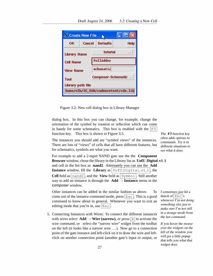
2. Select File → New → Cell View from the Library Managermenu. TheCreate New Filewindow appears. TheLibrary Namefield should be filled in astutorial and the Cell Namefield asFullAdder .
ChooseComposer - Schematicfrom the Tool list and the view nameshould be automatically filled asSchematic. This window is shownin Figure 3.2. Click OK.
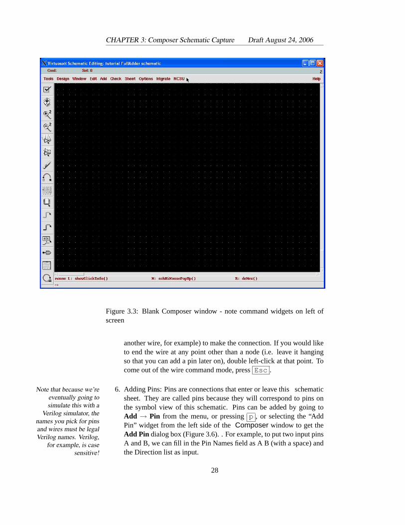
3. A blank Composer schematic editing window appears which lookslike that in Figure 3.3.
4. Adding Instances: An instance (either a gate from the standard cellMany of the keyboardkeys are bound to
“hotkeys” which causeactions to happen. You
can see these bindings inthe menus.
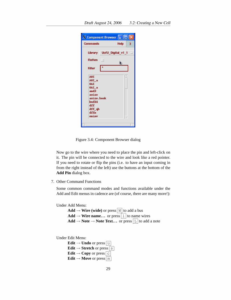
library, or a cell that you’ve designed earlier) can be placed in theschematic by selectingAdd → Instanceor pressing i on the key-board, and theComponent Browserdialog appears (shown in Fig-ure 3.4). Choose a library from theLibrary list and then choose thecell from the list box and the outline of the component’s symbol willappear when your curser is in the schematic window. Left clicks willadd instances of that cell to your schematic.
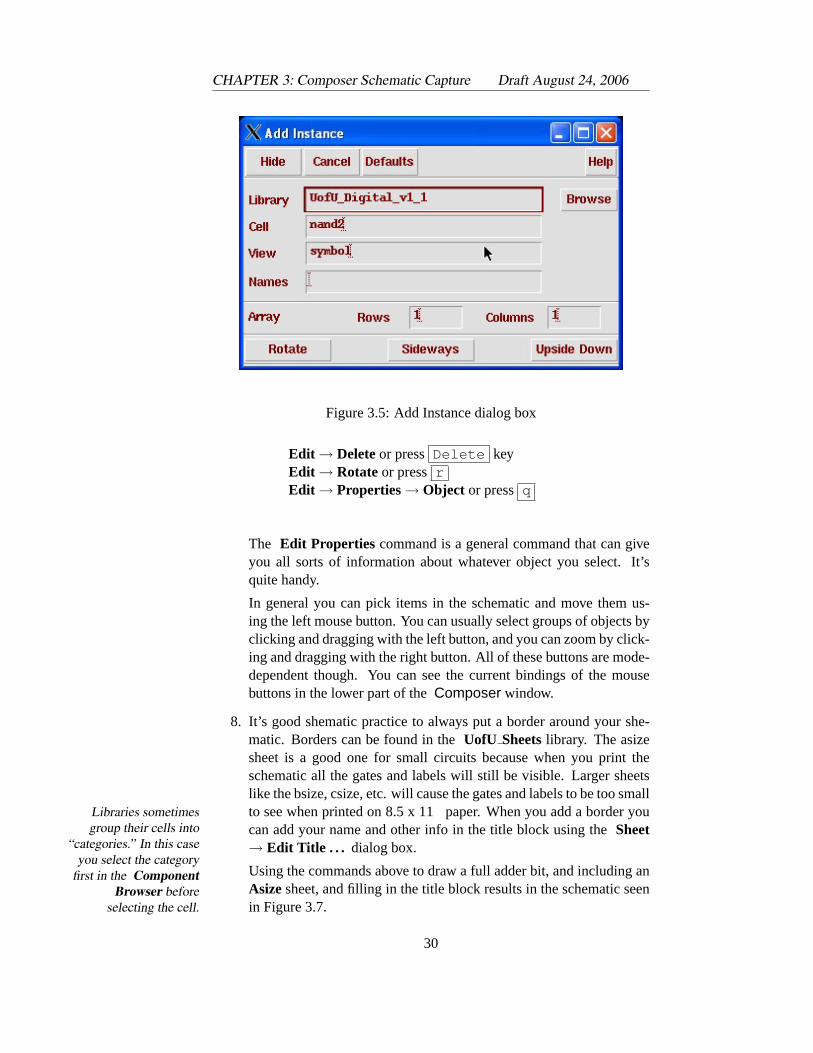
Additional options can be seen by popping up theAdd Instance
26
Draft August 24, 2006 3.2: Creating a New Cell
Figure 3.2: New cell dialog box in Library Manager
dialog box. In this box you can change, for example, change theorientation of the symbol by rotation or reflection which can comein handy for some schematics. This box is enabled with theF3function key. This box is shown in Figure 3.5. The F3 function key
often adds options tocommands. Try it indifferent situations tosee what it does.
The instances you should add are “symbol views” of the instances.There are lots of “views” of cells that all have different features, butfor schematics, symbols are what you want.
For example to add a 2-input NAND gate use the theComponentBrowserwindow, chose the library in the Library list asUofU Digital v1 1and cell in the list box asnand2. Alternately you can use theAddInstance window, fill the Library as UofU Digital v1 1 , the
Cell field as nand2 , and theView field as Symbol . Still anotherway to add an instance is through theAdd → Instancemenu in thecomposer window.
Other instances can be added in the similar fashion as above. ToI sometimes just hit abunch of Esc ’swhenever I’m not doingsomething else just tomake sure I’m not stillin a strange mode fromthe last command.
come out of the instance command mode, pressEsc . This is a goodcommand to know about in general. Whenever you want to exit anediting mode that you’re in, useEsc .
5. Connecting Instances with Wires: To connect the different instanceswith wires selectAdd → Wire (narrow) , or pressw to activate thewire command, or select the “narrow wire” widget from the toolbarIf you hover the mouse
over the widgets on theleft of the window youwill get a little popupthat tells you what thatwidget does.
on the left (it looks like a narrow wire . . . ). Now go to a connectionpoint of the gate instance and left-click on it to draw the wire and left-click on another connection point (another gate’s input or output, or
27
CHAPTER 3: Composer Schematic Capture Draft August 24, 2006
Figure 3.3: Blank Composer window - note command widgets on left ofscreen
another wire, for example) to make the connection. If you would liketo end the wire at any point other than a node (i.e. leave it hangingso that you can add a pin later on), double left-click at that point. Tocome out of the wire command mode, pressEsc .
6. Adding Pins: Pins are connections that enter or leave this schematicNote that because we’reeventually going tosimulate this with a
Verilog simulator, thenames you pick for pinsand wires must be legalVerilog names. Verilog,
for example, is casesensitive!
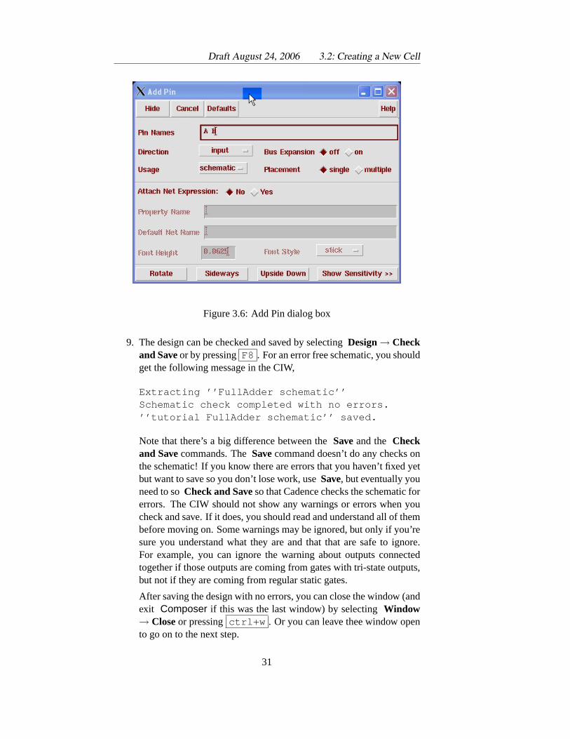
sheet. They are called pins because they will correspond to pins onthe symbol view of this schematic. Pins can be added by going toAdd → Pin from the menu, or pressingp , or selecting the “AddPin” widget from the left side of theComposer window to get theAdd Pin dialog box (Figure 3.6). . For example, to put two input pinsA and B, we can fill in the Pin Names field as A B (with a space) andthe Direction list as input.
28
Draft August 24, 2006 3.2: Creating a New Cell
Figure 3.4: Component Browser dialog
Now go to the wire where you need to place the pin and left-click onit. The pin will be connected to the wire and look like a red pointer.If you need to rotate or flip the pins (i.e. to have an input coming infrom the right instead of the left) use the buttons at the bottom of theAdd Pin dialog box.
7. Other Command Functions
Some common command modes and functions available under theAdd and Edit menus in cadence are (of course, there are many more!):
Under Add Menu:Add → Wire (wide) or pressW to add a busAdd → Wire name. . . or press l to name wiresAdd → Note→ Note Text. . . or pressL to add a note
Under Edit Menu:Edit → Undo or pressuEdit → Stretch or presssEdit → Copy or presscEdit → Move or pressm
29
CHAPTER 3: Composer Schematic Capture Draft August 24, 2006
Figure 3.5: Add Instance dialog box
Edit → Deleteor pressDelete keyEdit → Rotateor press rEdit → Properties→ Object or pressq
The Edit Properties command is a general command that can giveyou all sorts of information about whatever object you select. It’squite handy.
In general you can pick items in the schematic and move them us-ing the left mouse button. You can usually select groups of objects byclicking and dragging with the left button, and you can zoom by click-ing and dragging with the right button. All of these buttons are mode-dependent though. You can see the current bindings of the mousebuttons in the lower part of theComposer window.
8. It’s good shematic practice to always put a border around your she-matic. Borders can be found in theUofU Sheetslibrary. The asizesheet is a good one for small circuits because when you print theschematic all the gates and labels will still be visible. Larger sheetslike the bsize, csize, etc. will cause the gates and labels to be too smallto see when printed on 8.5 x 11 paper. When you add a border youLibraries sometimes
group their cells into“categories.” In this case
you select the categoryfirst in the Component
Browser beforeselecting the cell.
can add your name and other info in the title block using theSheet→ Edit Title . . . dialog box.
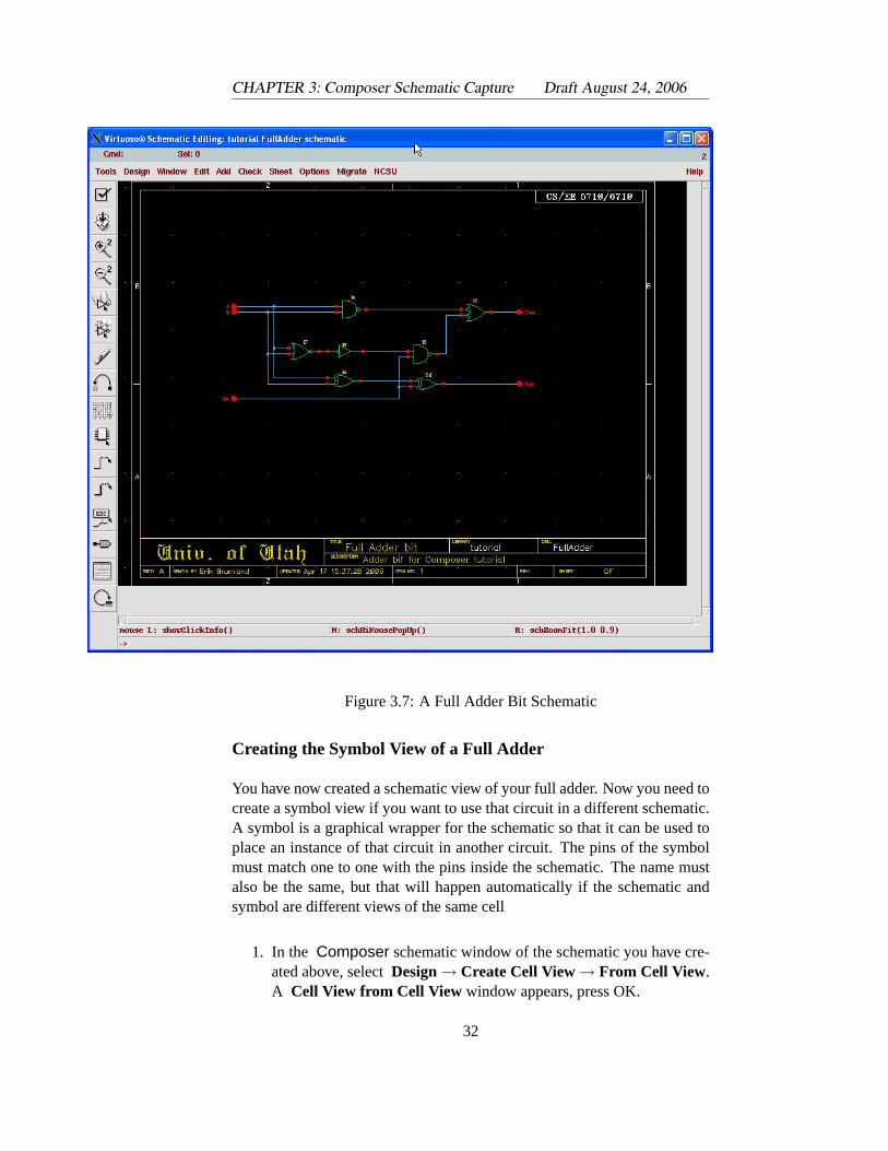
Using the commands above to draw a full adder bit, and including anAsizesheet, and filling in the title block results in the schematic seenin Figure 3.7.
30
Draft August 24, 2006 3.2: Creating a New Cell
Figure 3.6: Add Pin dialog box
9. The design can be checked and saved by selectingDesign→ Checkand Saveor by pressingF8 . For an error free schematic, you shouldget the following message in the CIW,
Extracting ’’FullAdder schematic’’Schematic check completed with no errors.’’tutorial FullAdder schematic’’ saved.
Note that there’s a big difference between theSaveand the Checkand Savecommands. TheSavecommand doesn’t do any checks onthe schematic! If you know there are errors that you haven’t fixed yetbut want to save so you don’t lose work, useSave, but eventually youneed to soCheck and Saveso that Cadence checks the schematic forerrors. The CIW should not show any warnings or errors when youcheck and save. If it does, you should read and understand all of thembefore moving on. Some warnings may be ignored, but only if you’resure you understand what they are and that that are safe to ignore.For example, you can ignore the warning about outputs connectedtogether if those outputs are coming from gates with tri-state outputs,but not if they are coming from regular static gates.
After saving the design with no errors, you can close the window (andexit Composer if this was the last window) by selectingWindow→ Closeor pressingctrl+w . Or you can leave thee window opento go on to the next step.
31
CHAPTER 3: Composer Schematic Capture Draft August 24, 2006
Figure 3.7: A Full Adder Bit Schematic
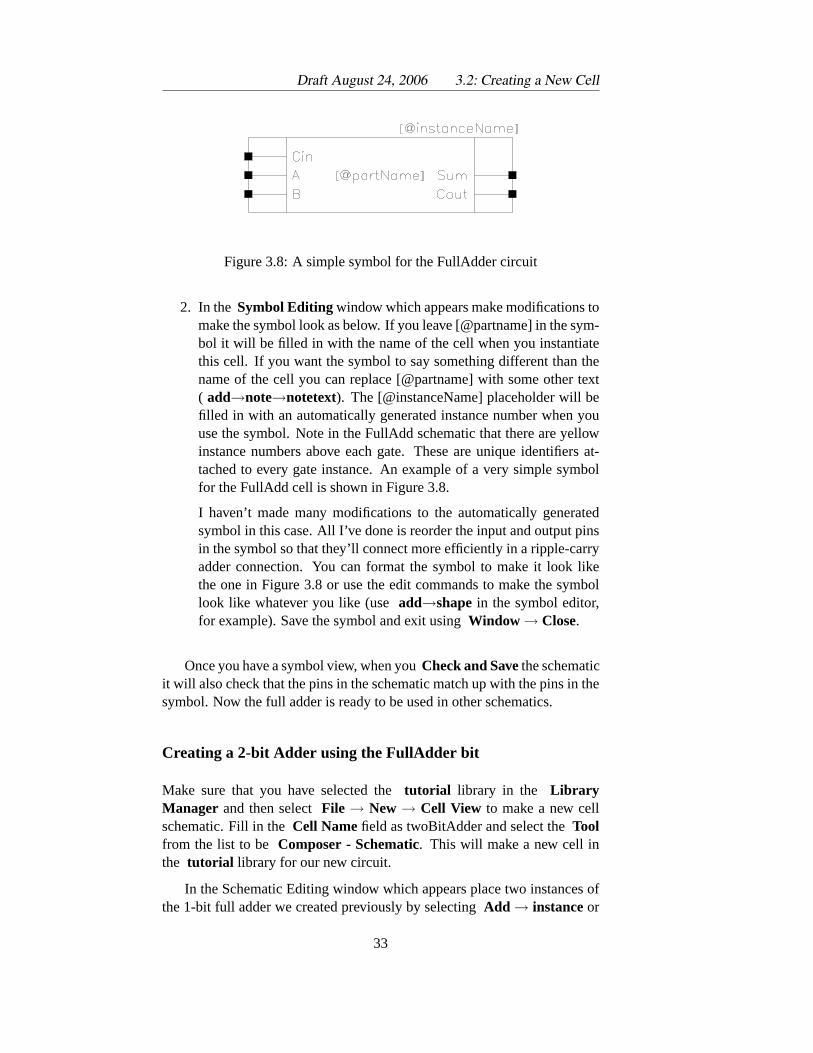
Creating the Symbol View of a Full Adder
You have now created a schematic view of your full adder. Now you need tocreate a symbol view if you want to use that circuit in a different schematic.A symbol is a graphical wrapper for the schematic so that it can be used toplace an instance of that circuit in another circuit. The pins of the symbolmust match one to one with the pins inside the schematic. The name mustalso be the same, but that will happen automatically if the schematic andsymbol are different views of the same cell
1. In the Composer schematic window of the schematic you have cre-ated above, selectDesign→ Create Cell View→ From Cell View.A Cell View from Cell View window appears, press OK.
32
Draft August 24, 2006 3.2: Creating a New Cell
Figure 3.8: A simple symbol for the FullAdder circuit
2. In the Symbol Editing window which appears make modifications tomake the symbol look as below. If you leave [@partname] in the sym-bol it will be filled in with the name of the cell when you instantiatethis cell. If you want the symbol to say something different than thename of the cell you can replace [@partname] with some other text( add→note→notetext). The [@instanceName] placeholder will befilled in with an automatically generated instance number when youuse the symbol. Note in the FullAdd schematic that there are yellowinstance numbers above each gate. These are unique identifiers at-tached to every gate instance. An example of a very simple symbolfor the FullAdd cell is shown in Figure 3.8.
I haven’t made many modifications to the automatically generatedsymbol in this case. All I’ve done is reorder the input and output pinsin the symbol so that they’ll connect more efficiently in a ripple-carryadder connection. You can format the symbol to make it look likethe one in Figure 3.8 or use the edit commands to make the symbollook like whatever you like (useadd→shapein the symbol editor,for example). Save the symbol and exit usingWindow → Close.
Once you have a symbol view, when youCheck and Savethe schematicit will also check that the pins in the schematic match up with the pins in thesymbol. Now the full adder is ready to be used in other schematics.
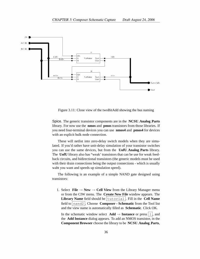
Creating a 2-bit Adder using the FullAdder bit
Make sure that you have selected thetutorial library in the LibraryManager and then selectFile → New→ Cell View to make a new cellschematic. Fill in theCell Namefield as twoBitAdder and select theToolfrom the list to be Composer - Schematic. This will make a new cell inthe tutorial library for our new circuit.
In the Schematic Editing window which appears place two instances ofthe 1-bit full adder we created previously by selectingAdd → instanceor
33
CHAPTER 3: Composer Schematic Capture Draft August 24, 2006
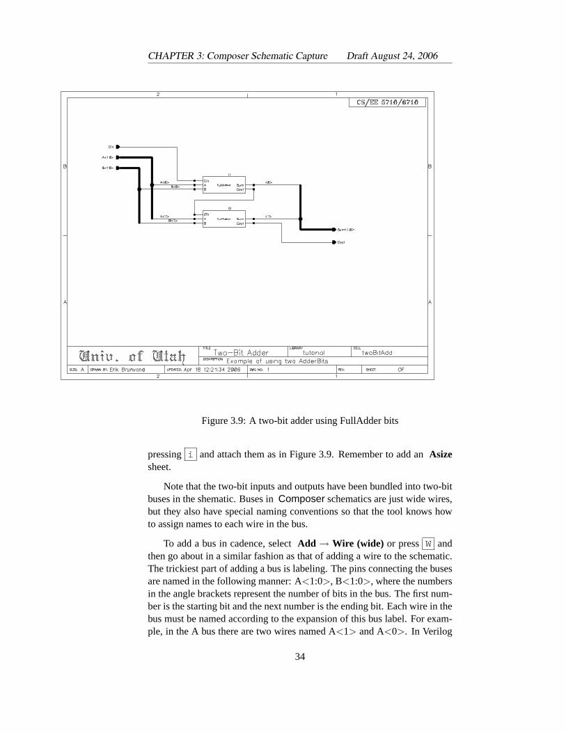
Figure 3.9: A two-bit adder using FullAdder bits
pressing i and attach them as in Figure 3.9. Remember to add anAsizesheet.
Note that the two-bit inputs and outputs have been bundled into two-bitbuses in the shematic. Buses inComposer schematics are just wide wires,but they also have special naming conventions so that the tool knows howto assign names to each wire in the bus.
To add a bus in cadence, selectAdd → Wire (wide) or press W andthen go about in a similar fashion as that of adding a wire to the schematic.The trickiest part of adding a bus is labeling. The pins connecting the busesare named in the following manner: A<1:0>, B<1:0>, where the numbersin the angle brackets represent the number of bits in the bus. The first num-ber is the starting bit and the next number is the ending bit. Each wire in thebus must be named according to the expansion of this bus label. For exam-ple, in the A bus there are two wires named A<1> and A<0>. In Verilog
34
Draft August 24, 2006 3.3: Schematics that use Transistors
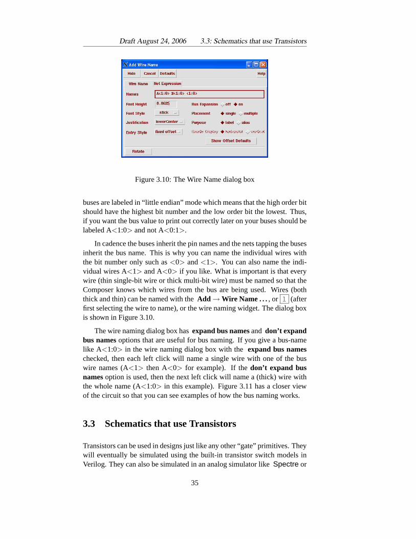
Figure 3.10: The Wire Name dialog box
buses are labeled in “little endian” mode which means that the high order bitshould have the highest bit number and the low order bit the lowest. Thus,if you want the bus value to print out correctly later on your buses should belabeled A<1:0> and not A<0:1>.
In cadence the buses inherit the pin names and the nets tapping the busesinherit the bus name. This is why you can name the individual wires withthe bit number only such as<0> and<1>. You can also name the indi-vidual wires A<1> and A<0> if you like. What is important is that everywire (thin single-bit wire or thick multi-bit wire) must be named so that theComposer knows which wires from the bus are being used. Wires (boththick and thin) can be named with theAdd →Wire Name . . ., or l (afterfirst selecting the wire to name), or the wire naming widget. The dialog boxis shown in Figure 3.10.
The wire naming dialog box hasexpand bus namesand don’t expandbus namesoptions that are useful for bus naming. If you give a bus-namelike A<1:0> in the wire naming dialog box with theexpand bus nameschecked, then each left click will name a single wire with one of the buswire names (A<1> then A<0> for example). If thedon’t expand busnamesoption is used, then the next left click will name a (thick) wire withthe whole name (A<1:0> in this example). Figure 3.11 has a closer viewof the circuit so that you can see examples of how the bus naming works.
3.3 Schematics that use Transistors
Transistors can be used in designs just like any other “gate” primitives. Theywill eventually be simulated using the built-in transistor switch models inVerilog. They can also be simulated in an analog simulator likeSpectre or
35
CHAPTER 3: Composer Schematic Capture Draft August 24, 2006
Figure 3.11: Close view of the twoBitAdd showing the bus naming
Spice. The generic transistor components are in theNCSU Analog Partslibrary. For now use thenmosand pmostransistors from those libraries. Ifyou need four-terminal devices you can usenmos4and pmos4for deviceswith an explicit bulk node connection.
These will netlist into zero-delay switch models when they are simu-lated. If you’d rather have unit-delay simulation of your transistor switchesyou can use the same devices, but from theUofU Analog Parts library.The UofU library also has “weak’ transistors that can be use for weak feed-back circuits, and bidirectional transistors (the generic models must be usedwith their drain connections being the output connections - which is usuallywaht you want and speeds up simulation speed).
The following is an example of a simple NAND gate designed usingtransistors:
1. Select File → New→ Cell View from the Library Manager menuor from the CIW menu. TheCreate New Filewindow appears. TheLibrary Name field should betutorial . Fill in the Cell Namefield to nand2 . ChooseComposer - Schematicfrom the Tool listand the view name is automatically filled asSchematic. Click OK.
In the schematic window selectAdd → Instance or press i , andthe Add Instancedialog appears. To add an NMOS transistor, in theComponent Browserchoose the library to beNCSU Analog Parts,
36
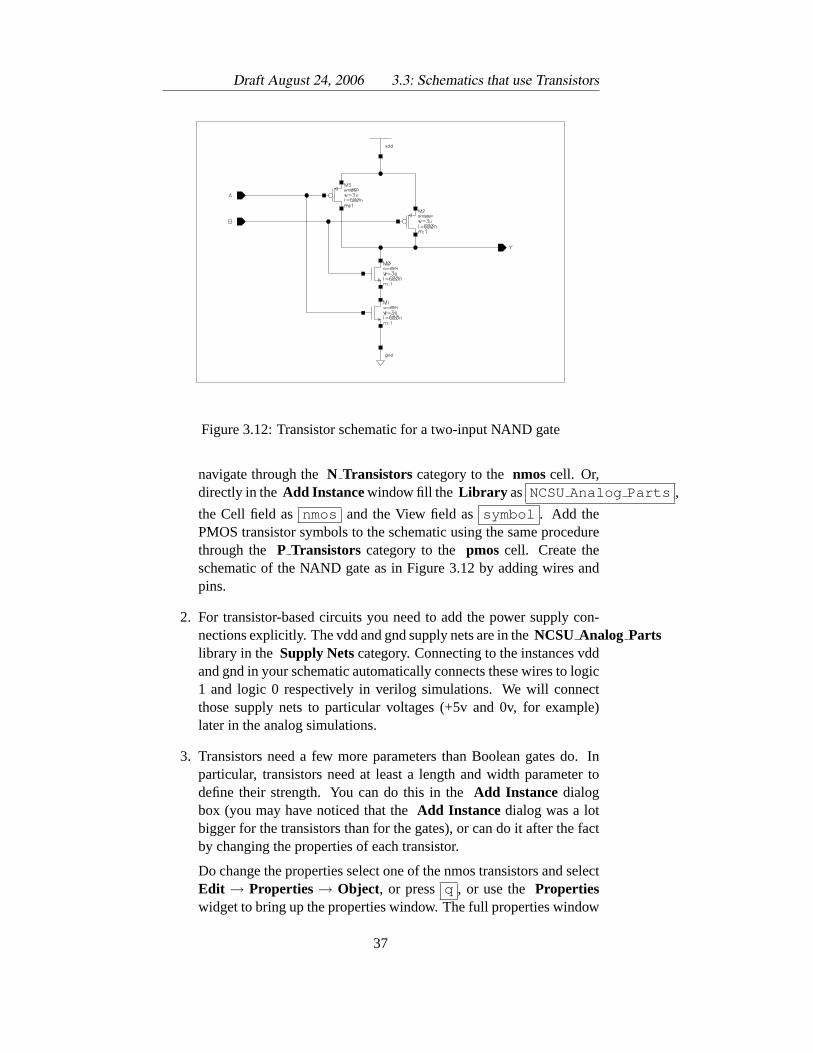
Draft August 24, 2006 3.3: Schematics that use Transistors
Figure 3.12: Transistor schematic for a two-input NAND gate
navigate through theN Transistors category to thenmoscell. Or,directly in theAdd Instancewindow fill the Library as NCSUAnalog Parts ,
the Cell field as nmos and the View field assymbol . Add thePMOS transistor symbols to the schematic using the same procedurethrough the P Transistors category to thepmos cell. Create theschematic of the NAND gate as in Figure 3.12 by adding wires andpins.
2. For transistor-based circuits you need to add the power supply con-nections explicitly. The vdd and gnd supply nets are in theNCSU Analog Partslibrary in the Supply Netscategory. Connecting to the instances vddand gnd in your schematic automatically connects these wires to logic1 and logic 0 respectively in verilog simulations. We will connectthose supply nets to particular voltages (+5v and 0v, for example)later in the analog simulations.
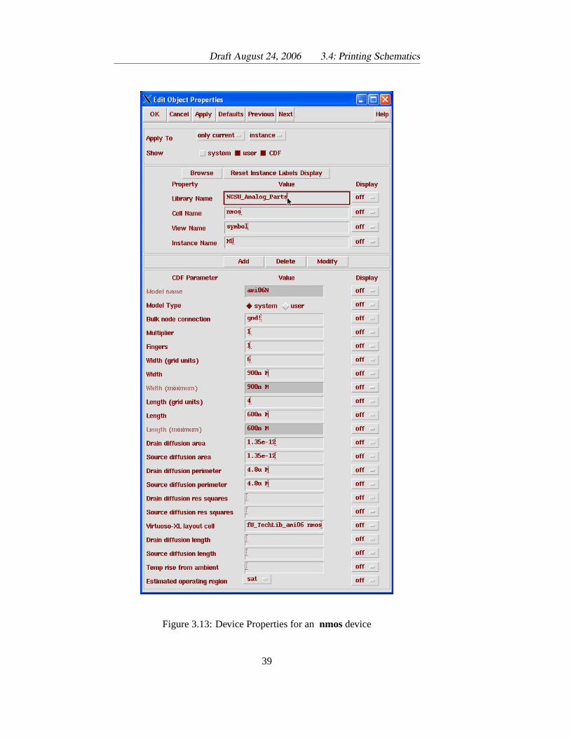
3. Transistors need a few more parameters than Boolean gates do. Inparticular, transistors need at least a length and width parameter todefine their strength. You can do this in theAdd Instance dialogbox (you may have noticed that theAdd Instance dialog was a lotbigger for the transistors than for the gates), or can do it after the factby changing the properties of each transistor.
Do change the properties select one of the nmos transistors and selectEdit → Properties→ Object, or press q , or use the Propertieswidget to bring up the properties window. The full properties window
37
CHAPTER 3: Composer Schematic Capture Draft August 24, 2006
is shown in Figure 3.13.
Change the properties of the nmos transistor by changing the Widthto 3u M (3 microns). Leave the length as600n M (0.6 microns).Similarly follow the steps for the pmos transistor with W/L = 3/0.6(i.e. W = 3u M amd L = 600n M ).
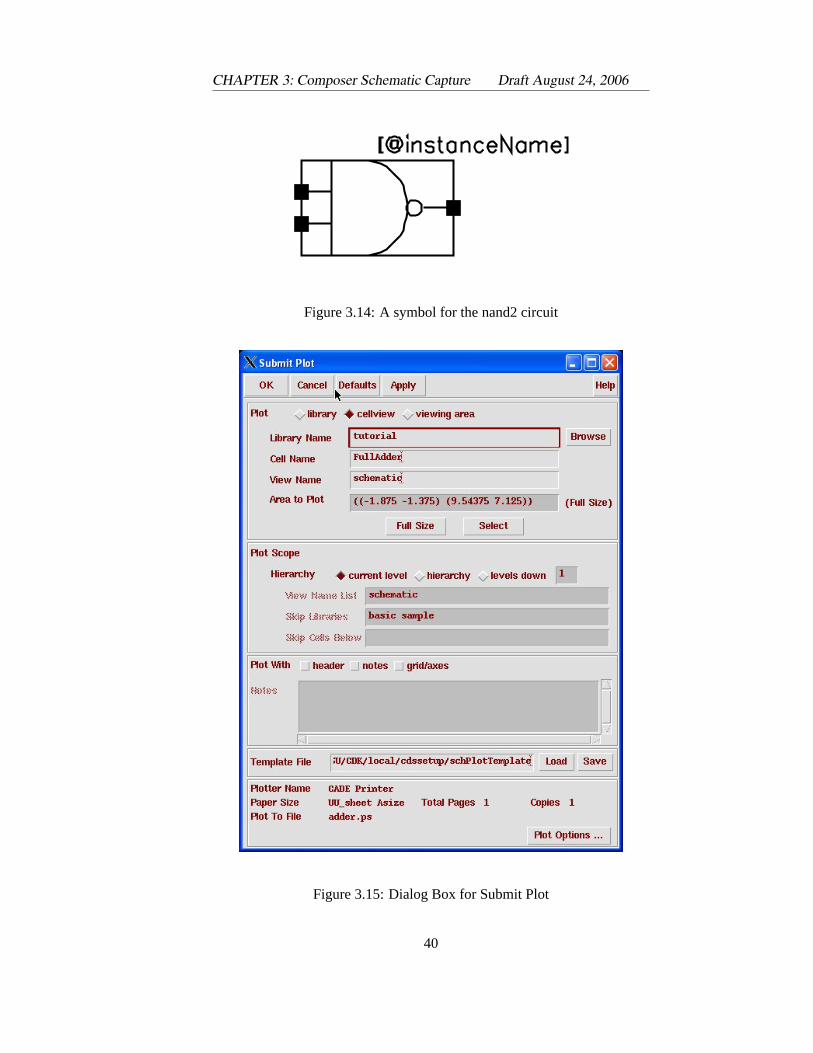
4. Create a symbol for the NAND gate by selectingDesign→ CreateCellView → From CellView. The Cadence-generated symbol willbe a simple rectangle. You can easily modify it to make it look likeFigure 3.14 using arcs and circles.
Note that in order to get the circle for the nand2 bubble to be the rightsize in proportion to the rest of the gate you may have to use a finergrid while you’re drawing that circle. You can change the grid size inthe Options→ Display Options dialog box, as theSnap Spacingvalue. But, when you’re done make sure that you set the snap gridback to 0.0625 so that the pins you make will match up properly withthe wires in the schematic!
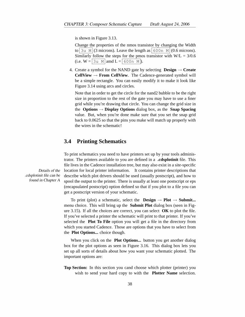
3.4 Printing Schematics
To print schematics you need to have printers set up by your tools adminis-trator. The printers available to you are defined in a.cdsplotinit file. Thisfile lives in the Cadence installation tree, but may also exist in a site-specificlocation for local printer information. It contains printer descriptions thatDetails of the
.cdsplotinit file can befound in Chapter A
describe which plot drivers should be used (usually postscript), and how tospool the output to the printer. There is usually at least one postscript or eps(encapsulated postscript) option defined so that if you plot to a file you canget a postscript version of your schematic.
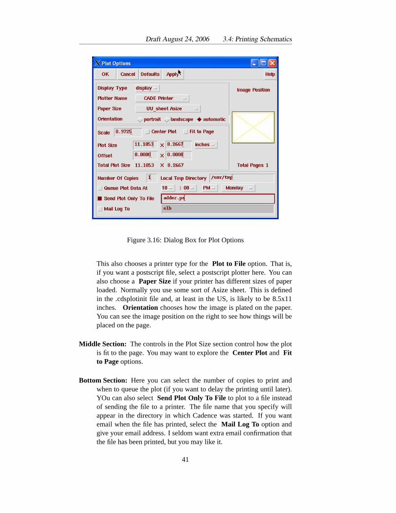
To print (plot) a schematic, select theDesign→ Plot → Submit...menu choice. This will bring up theSubmit Plot dialog box (seen in Fig-ure 3.15). If all the choices are correct, you can selectOK to plot the file.If you’ve selected a printer the schematic will print to that printer. If you’veselected thePlot To File option you will get a file in the directory fromwhich you started Cadence. Those are options that you have to select fromthe Plot Options... choice though.
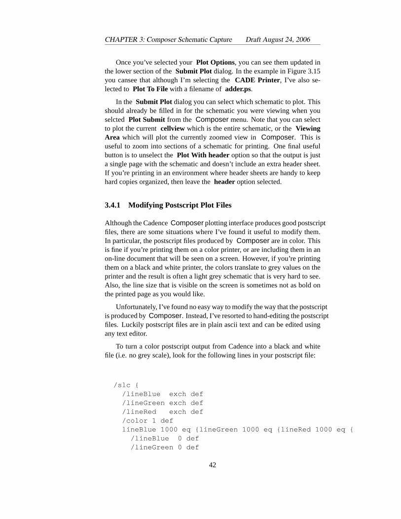
When you click on thePlot Options... button you get another dialogbox for the plot options as seen in Figure 3.16. This dialog box lets youset up all sorts of details about how you want your schematic plotted. Theimportant options are:
Top Section: In this section you cand choose which plotter (printer) youwish to send your hard copy to with thePlotter Name selection.
38
Draft August 24, 2006 3.4: Printing Schematics
Figure 3.13: Device Properties for annmosdevice
39
CHAPTER 3: Composer Schematic Capture Draft August 24, 2006
Figure 3.14: A symbol for the nand2 circuit
Figure 3.15: Dialog Box for Submit Plot
40
Draft August 24, 2006 3.4: Printing Schematics
Figure 3.16: Dialog Box for Plot Options
This also chooses a printer type for thePlot to File option. That is,if you want a postscript file, select a postscript plotter here. You canalso choose aPaper Sizeif your printer has different sizes of paperloaded. Normally you use some sort of Asize sheet. This is definedin the .cdsplotinit file and, at least in the US, is likely to be 8.5x11inches. Orientation chooses how the image is plated on the paper.You can see the image position on the right to see how things will beplaced on the page.
Middle Section: The controls in the Plot Size section control how the plotis fit to the page. You may want to explore theCenter Plot and Fitto Pageoptions.
Bottom Section: Here you can select the number of copies to print andwhen to queue the plot (if you want to delay the printing until later).YOu can also selectSend Plot Only To File to plot to a file insteadof sending the file to a printer. The file name that you specify willappear in the directory in which Cadence was started. If you wantemail when the file has printed, select theMail Log To option andgive your email address. I seldom want extra email confirmation thatthe file has been printed, but you may like it.
41
CHAPTER 3: Composer Schematic Capture Draft August 24, 2006
Once you’ve selected yourPlot Options, you can see them updated inthe lower section of theSubmit Plot dialog. In the example in Figure 3.15you cansee that although I’m selecting theCADE Printer , I’ve also se-lected to Plot To File with a filename ofadder.ps.
In the Submit Plot dialog you can select which schematic to plot. Thisshould already be filled in for the schematic you were viewing when youselcted Plot Submit from the Composer menu. Note that you can selectto plot the currentcellview which is the entire schematic, or theViewingArea which will plot the currently zoomed view inComposer. This isuseful to zoom into sections of a schematic for printing. One final usefulbutton is to unselect thePlot With header option so that the output is justa single page with the schematic and doesn’t include an extra header sheet.If you’re printing in an environment where header sheets are handy to keephard copies organized, then leave theheaderoption selected.
3.4.1 Modifying Postscript Plot Files
Although the CadenceComposer plotting interface produces good postscriptfiles, there are some situations where I’ve found it useful to modify them.In particular, the postscript files produced byComposer are in color. Thisis fine if you’re printing them on a color printer, or are including them in anon-line document that will be seen on a screen. However, if you’re printingthem on a black and white printer, the colors translate to grey values on theprinter and the result is often a light grey schematic that is very hard to see.Also, the line size that is visible on the screen is sometimes not as bold onthe printed page as you would like.
Unfortunately, I’ve found no easy way to modify the way that the postscriptis produced byComposer. Instead, I’ve resorted to hand-editing the postscriptfiles. Luckily postscript files are in plain ascii text and can be edited usingany text editor.
To turn a color postscript output from Cadence into a black and whitefile (i.e. no grey scale), look for the following lines in your postscript file:
/slc {/lineBlue exch def/lineGreen exch def/lineRed exch def/color 1 deflineBlue 1000 eq {lineGreen 1000 eq {lineRed 1000 eq {
/lineBlue 0 def/lineGreen 0 def
42
Draft August 24, 2006 3.5: Variable, Pin, and Cell Naming Restrictions
/lineRed 0 def} if} if} if
} def
/sfc {/fillBlue exch def/fillGreen exch def/fillRed exch def/color 1 deffillBlue 1000 eq {fillGreen 1000 eq {fillRed 1000 eq {
/fillBlue 0 def/fillGreen 0 def/fillRed 0 def
} if} if} if} def
Change all the lines that read/color 1 def to be/color 0 defand the schematic will print in black and white with no color or grey scaleapproximation of color.
To change the thickness of the lines in the postscript file, look for thepostscript function:
/ssls { [] 0 setdash1 setlinewidth
} def
This sets the default line width to 1 point. If you increase the value ofthe line width to 3 or 4 you will get a bolder line in your schematic. Thesehacks can make much better looking schematics in hardcopy or to includein another document. Of course, depending on which other document youare including the graphics into you may need to convert the postscript intosome other format such as pdf (ps2pdf) or jpg (I use Illustrator on a PC forthis trick. The xv program on linux also works.).
3.5 Variable, Pin, and Cell Naming Restrictions
Although it’s not obvious at the moment, all the simulation in the CadencedfII environment is through Verilog simulators. So, althoughComposerallows wire and pin names that aren’t legal Verilog names, your life will bemucheasier if you only use Verilog-compatable names withinComposer.This means that names must start with a letter, and can then consist of let-ters, numbers, and underscores (thecharacter) only. Do not use dashes or
43
CHAPTER 3: Composer Schematic Capture Draft August 24, 2006
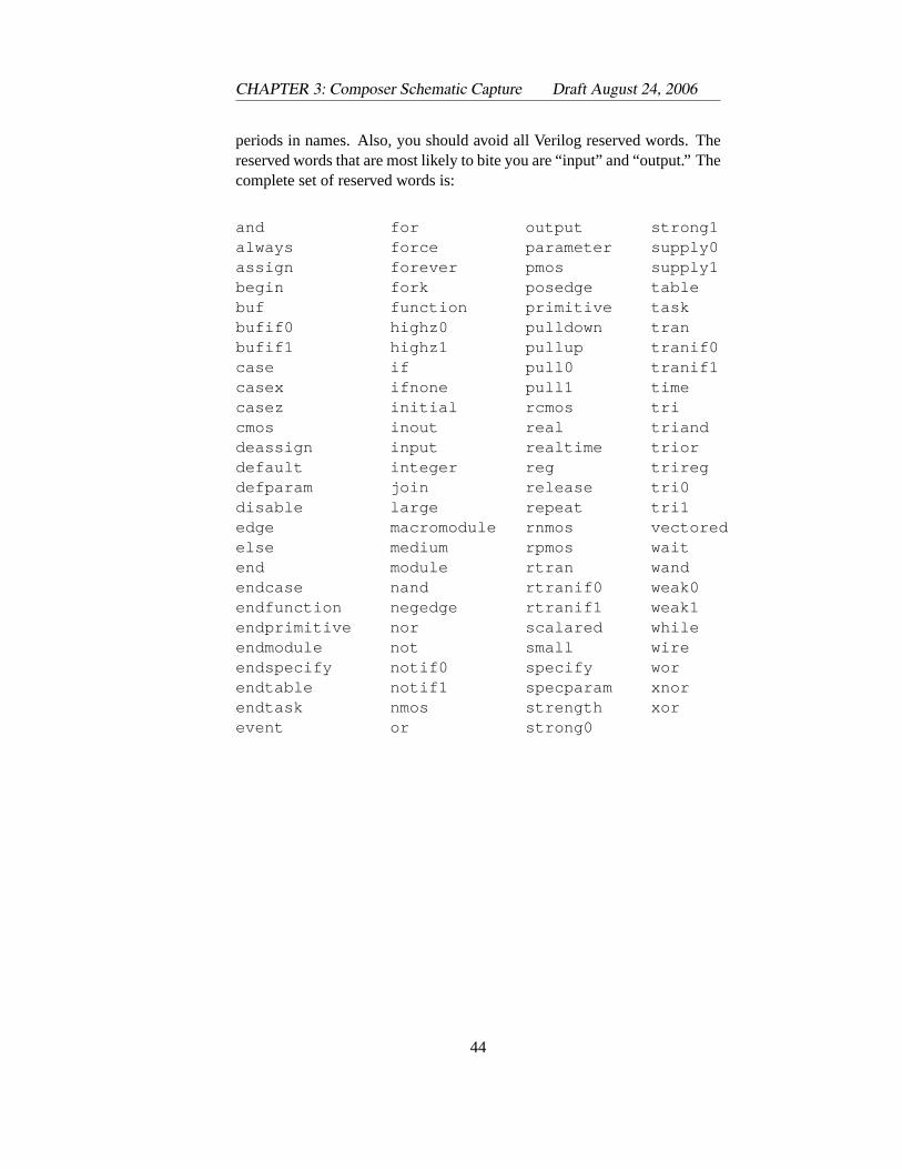
periods in names. Also, you should avoid all Verilog reserved words. Thereserved words that are most likely to bite you are “input” and “output.” Thecomplete set of reserved words is:
and for output strong1always force parameter supply0assign forever pmos supply1begin fork posedge tablebuf function primitive taskbufif0 highz0 pulldown tranbufif1 highz1 pullup tranif0case if pull0 tranif1casex ifnone pull1 timecasez initial rcmos tricmos inout real trianddeassign input realtime triordefault integer reg triregdefparam join release tri0disable large repeat tri1edge macromodule rnmos vectoredelse medium rpmos waitend module rtran wandendcase nand rtranif0 weak0endfunction negedge rtranif1 weak1endprimitive nor scalared whileendmodule not small wireendspecify notif0 specify worendtable notif1 specparam xnorendtask nmos strength xorevent or strong0
44
Chapter 4
Verilog Simulation
A HARDWARE DESCRIPTIONLANGUAGE (HDL) is a programminglanguage designed specifically to describe digital hardware. Typ-ical HDLs look somewhat like software programming languages
in terms of syntax, but have very different semantics for interpreting thelanguage statements. Digital hardware, when examined at a sufficient levelof detail, is described as a set of Boolean operators executing concurrently.These Boolean operators may be complex Boolean functions, refined intosets of Boolean gates (NAND, NOR, etc.), or described in terms of the in-dividual transistors that implement the functions, but fundamentally digitalsystems operate through the combined effect of these Boolean operatorsexecuting at the same time. There may be a few hundred gates or tran-sistors, or there may be tens of millions, but because of the concurrencyinherent in these systems an HDL used to describe these systems must beable to support this sort of concurrent behavior. Of course, they also support“software-like” sequential behavior for high-level modeling, but they mustalso support the very concurrent behavior of the fine-grained descriptions.
To enable this sort of behavior, HDLs are typically executed throughevent-driven simulators. An event-driven simulator uses a notion of simu-lation time and an event-queue to schedule events in the system being de-scribed. Each HDL construct (think of a construct as modeling a single gate,for example, but it could be much more complex than that) has inputs andoutputs. The description of the construct includes not only the function ofthe construct, but how the construct reacts over time. If a signal changesthen the event-queue looks up which constructs are affected by that changeto know which code to run. That code may produce a new event at the con-struct’s output, and that output event will be sent to the event queue so thatthe output event will happen sometime in the future. When simulation timeadvances to the correct value the output event occurs which may cause otheractivity in the described system. The event-queue is the central controlling
CHAPTER 4: Verilog Simulation Draft August 24, 2006
structure that enables the HDL program to behave like the hardware that itis describing. So, although you may think of “running a program” writtenin a software programming language, it’s more correct to think of “runninga simulation” when executing an HDL program.
Verilog is one of the two most widely used Hardware Description Lan-guages with VHDL being the other main HDL in wide use today. Much ofthe simulation information described in this chapter will translate reason-One reason to choose
Verilog is that some ofthe tools in this CAD
flow, place and route inparticular, require
Verilog as an inputspecification.
ably easily to VHDL simulators, but for this text I’ll stick with Verilog. Thechoice of using Verilog is somewhat arbitrary as the two languages are quitesimilar in their ability to describe digital systems. In very general terms,many designers find Verilog syntax simpler and easier to use, at the expenseof VHDL’s richer type system, but both HDLs are used on “real” designs.
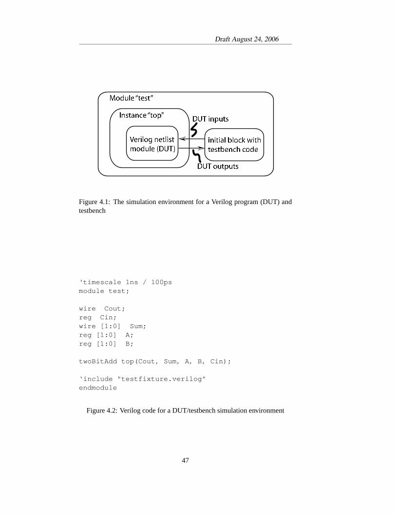
Verilog program execution (program simulation) requires a Verilog sim-ulator that implements the event-driven semantics of the language. Youwill also need a method of sending inputs to your program, and a meansof checking that the outputs of your Verilog program are correct. This isusually accomplished using a second Verilog program known as atestbenchor testfixture. This is similar to how integrated circuits are tested. In thatcase the chip to be tested is called the Device Under Test (DUT), and theDUT is connected to a testbench that drives the DUT inputs and records andcompares the DUT outputs to some expected values. If we use the sameterminology for our Verilog simulations, then the Verilog program that youwant to run would be the equivalent of the DUT, and you need to write atestbench program (also in Verilog) to drive the program inputs and look atthe program outputs.
This general scheme is shown in Figures 4.1 and 4.2. These figures showthe test environment that is created by theComposer system, but they area good general testbench format. There is a top-level module namedtestthat is simulated. This module includes one instance of the DUT. In thiscase the DUT is our twoBitAdd module from Chapter 3 and the instancename is top. It also includes testfixture code in a separate file namedtest-fixture.verilog. In this file is an initial block that has the testfixture code.Example testfixture code will be seen in the following sections of this Chap-ter. Note that the moduletestdefines all the inputs to the DUT asreg type,and outputs from the DUT aswire type. This is because the testfixturewants to set the value of the DUT inputs and look at the value of the DUToutputs.
This text does not include a tutorial on the Verilog language. There arelots of good Verilog overviews out there, including Appendix A of the classtextbookCMOS VLSI Design: A Circuits and Systems Perspective, 3rded by Weste and Harris [1]. I’ll show some examples of Verilog code andtestbench code, but for a basic introduction see Appendix A in that book, or
46
Draft August 24, 2006
Figure 4.1: The simulation environment for a Verilog program (DUT) andtestbench
‘timescale 1ns / 100psmodule test;
wire Cout;reg Cin;wire [1:0] Sum;reg [1:0] A;reg [1:0] B;
twoBitAdd top(Cout, Sum, A, B, Cin);
‘include "testfixture.verilog"endmodule
Figure 4.2: Verilog code for a DUT/testbench simulation environment
47
CHAPTER 4: Verilog Simulation Draft August 24, 2006
any of the good Verilog introductions on the web.
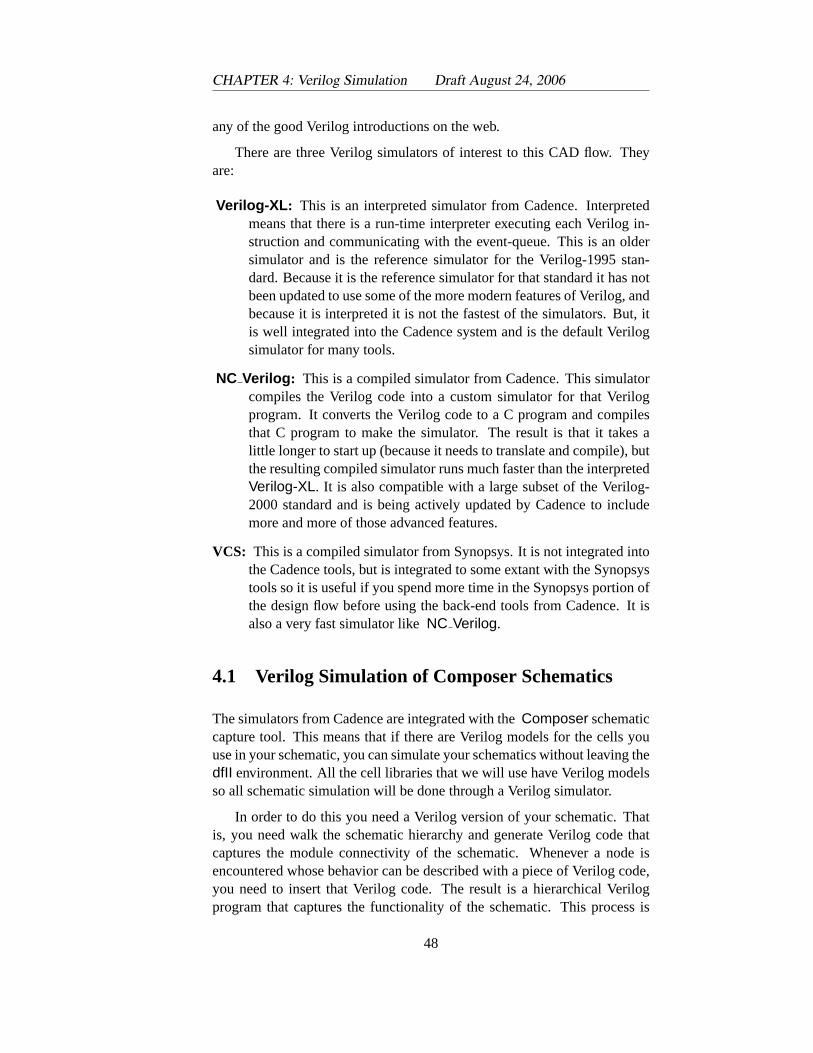
There are three Verilog simulators of interest to this CAD flow. Theyare:
Verilog-XL : This is an interpreted simulator from Cadence. Interpretedmeans that there is a run-time interpreter executing each Verilog in-struction and communicating with the event-queue. This is an oldersimulator and is the reference simulator for the Verilog-1995 stan-dard. Because it is the reference simulator for that standard it has notbeen updated to use some of the more modern features of Verilog, andbecause it is interpreted it is not the fastest of the simulators. But, itis well integrated into the Cadence system and is the default Verilogsimulator for many tools.
NC Verilog : This is a compiled simulator from Cadence. This simulatorcompiles the Verilog code into a custom simulator for that Verilogprogram. It converts the Verilog code to a C program and compilesthat C program to make the simulator. The result is that it takes alittle longer to start up (because it needs to translate and compile), butthe resulting compiled simulator runs much faster than the interpretedVerilog-XL. It is also compatible with a large subset of the Verilog-2000 standard and is being actively updated by Cadence to includemore and more of those advanced features.
VCS: This is a compiled simulator from Synopsys. It is not integrated intothe Cadence tools, but is integrated to some extant with the Synopsystools so it is useful if you spend more time in the Synopsys portion ofthe design flow before using the back-end tools from Cadence. It isalso a very fast simulator likeNC Verilog.
4.1 Verilog Simulation of Composer Schematics
The simulators from Cadence are integrated with theComposer schematiccapture tool. This means that if there are Verilog models for the cells youuse in your schematic, you can simulate your schematics without leaving thedfII environment. All the cell libraries that we will use have Verilog modelsso all schematic simulation will be done through a Verilog simulator.
In order to do this you need a Verilog version of your schematic. Thatis, you need walk the schematic hierarchy and generate Verilog code thatcaptures the module connectivity of the schematic. Whenever a node isencountered whose behavior can be described with a piece of Verilog code,you need to insert that Verilog code. The result is a hierarchical Verilogprogram that captures the functionality of the schematic. This process is
48
Draft August 24, 2006 4.1: Verilog Simulation of ComposerSchematics
known asnetlisting, and the result is a structural Verilog description that isalso sometimes called anetlist. According to Figure 4.1 this netlist couldalso be known as the DUT. Once you have the DUT code, you need to writetestbench code to communicate with the DUT during simulation.
Fortunately theComposer-Verilog integration environment will gen-erate a simulatable netlist for you from the schematic, and also generatea template for a testbench file. The netlisting process walks through yourhierarchical schematic and generates a program that describes the hierar-chy. If the netlister encounters abehavioral cell view, that view containsVerilog code that describes that module’s function so the code in thebe-havioral view is added to the netlist. If a schematic uses transistors fromthe NCSU Analog Parts or UofU Analog Parts libraries, those transis-tors are replaced with Verilog transistor models. The Verilog transistorprimitives are built into the Verilog language and simulate the transistorsas switches. We use thecmosschview to signal to the netlister that this isa leaf cell that contains only transistors.
These two different description techniques for leaf cells (behavioraland transistorcmossch) can be mixed in a single schematic, and in factif the leaf cells have bothbehavioral (Verilog) and cmossch (transistor)views you can choose which low-level behavior is simulated by manipu-lating the netlisting procedure inComposer. This is useful because eachtype of simulation has its own advantages and disadvantages. Behavioralmodeling can simulate more quickly, and allows back-annotation of timingfrom other tools like synthesis tools though a Standard Delay Format (sdf)file (described in more detail in Section 4.4 and in Chapter 8). Switch levelmodeling can be a more accurate simulation of the low level details of thecircuit’s operation and can expose problems that are not visible in the morehigh-level behavioral simulation.
4.1.1 Verilog-XL : Simulating a Schematic
As an example of simulating a schematic usingVerilog-XL we’ll use thetwo-bit adder from Chapter 3. To startVerilog-XL simulation you can usethe CIW window by going toTools→ Verilog Integration → Verilog-XL.... The Setup Environment window appears in which the Run Direc-tory, Library, Cell and View fields need to be filled. Press OK.
Or (the much easier way) open up theComposer schematic of the It is very important tohave a separate rundirectory for eachdifferent design, but youcan keep the same rundirectory for differentsimulations of the samedesign.
two-bit adder using the library browser and in theComposer schematicediting window, selectTools→ Simulation → Verilog-XL . The SetupEnvironment window appears with all the fields filled. TheRun Directorycan be changed or left as default<designname>.run1. A dialog box forsimulation of the two-bit adder from Chapter 3 is shown in Figure 4.3. Press
49
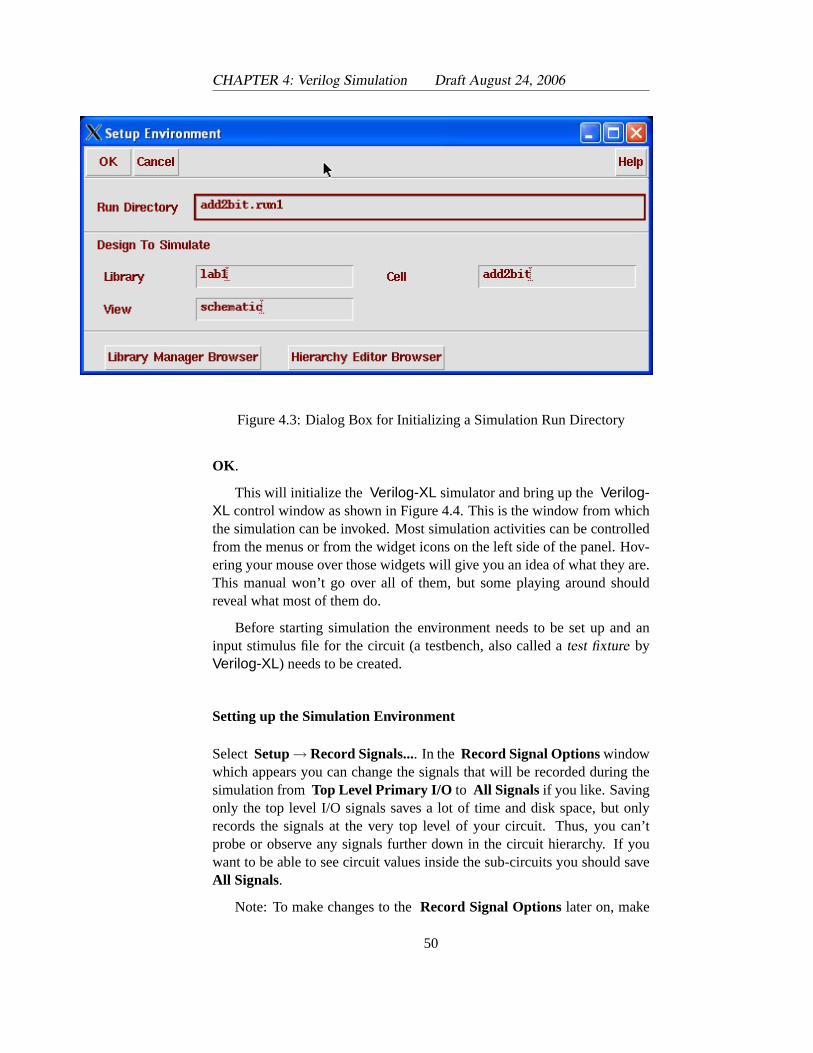
CHAPTER 4: Verilog Simulation Draft August 24, 2006
Figure 4.3: Dialog Box for Initializing a Simulation Run Directory
OK .
This will initialize the Verilog-XL simulator and bring up theVerilog-XL control window as shown in Figure 4.4. This is the window from whichthe simulation can be invoked. Most simulation activities can be controlledfrom the menus or from the widget icons on the left side of the panel. Hov-ering your mouse over those widgets will give you an idea of what they are.This manual won’t go over all of them, but some playing around shouldreveal what most of them do.
Before starting simulation the environment needs to be set up and aninput stimulus file for the circuit (a testbench, also called atest fixture byVerilog-XL) needs to be created.
Setting up the Simulation Environment
SelectSetup→Record Signals.... In the Record Signal Optionswindowwhich appears you can change the signals that will be recorded during thesimulation fromTop Level Primary I/O to All Signals if you like. Savingonly the top level I/O signals saves a lot of time and disk space, but onlyrecords the signals at the very top level of your circuit. Thus, you can’tprobe or observe any signals further down in the circuit hierarchy. If youwant to be able to see circuit values inside the sub-circuits you should saveAll Signals.
Note: To make changes to theRecord Signal Optionslater on, make
50
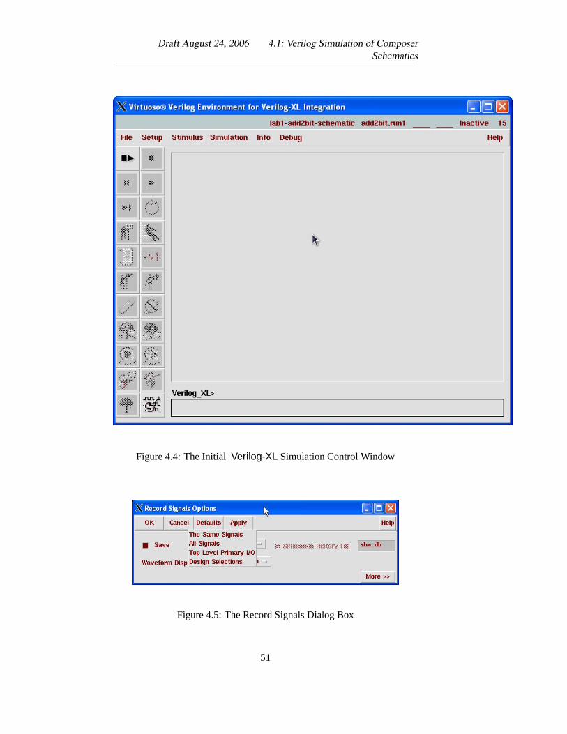
Draft August 24, 2006 4.1: Verilog Simulation of ComposerSchematics
Figure 4.4: The InitialVerilog-XL Simulation Control Window
Figure 4.5: The Record Signals Dialog Box
51
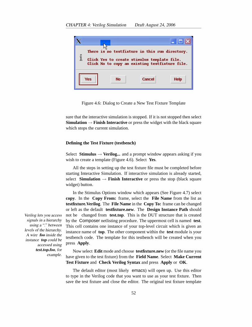
CHAPTER 4: Verilog Simulation Draft August 24, 2006
Figure 4.6: Dialog to Create a New Test Fixture Template
sure that the interactive simulation is stopped. If it is not stopped then selectSimulation→ Finish Interactive or press the widget with the black squarewhich stops the current simulation.
Defining the Test Fixture (testbench)
Select Stimulus→ Verilog... and a prompt window appears asking if youwish to create a template (Figure 4.6). SelectYes.
All the steps in setting up the test fixture file must be completed beforestarting Interactive Simulation. If interactive simulation is already started,select Simulation → Finish Interactive or press the stop (black squarewidget) button.
In the Stimulus Options window which appears (See Figure 4.7) selectcopy. In the Copy From: frame, select theFile Name from the list astestfixture.Verilog. The File Namein the Copy To: frame can be changedor left as the defaulttestfixture.new. The Design Instance Pathshouldnot be changed fromtest.top. This is the DUT structure that is createdVerilog lets you access
signals in a hierarchyusing a “.” between
levels of the hierarchy.A wire foo inside theinstance top could be
accessed usingtest.top.foo, for
example.
by the Composer netlisting procedure. The uppermost cell is namedtest.This cell contains one instance of your top-level circuit which is given aninstance name oftop. The other component within thetestmodule is yourtestbench code. The template for this testbench will be created when youpressApply .
Now selectEdit mode and choosetestfixture.new(or the file name youhave given to the test fixture) from theField Name. SelectMake CurrentTest Fixture and Check Verilog Syntaxand pressApply or OK .
The default editor (most likelyemacs) will open up. Use this editorto type in the Verilog code that you want to use as your test fixture. Thensave the test fixture and close the editor. The original test fixture template
52
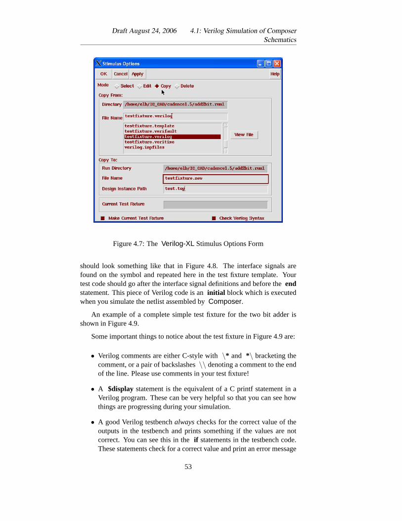
Draft August 24, 2006 4.1: Verilog Simulation of ComposerSchematics
Figure 4.7: TheVerilog-XL Stimulus Options Form
should look something like that in Figure 4.8. The interface signals arefound on the symbol and repeated here in the test fixture template. Yourtest code should go after the interface signal definitions and before theendstatement. This piece of Verilog code is aninitial block which is executedwhen you simulate the netlist assembled byComposer.
An example of a complete simple test fixture for the two bit adder isshown in Figure 4.9.
Some important things to notice about the test fixture in Figure 4.9 are:
• Verilog comments are either C-style with\* and *\ bracketing thecomment, or a pair of backslashes\\ denoting a comment to the endof the line. Please use comments in your test fixture!
• A $display statement is the equivalent of a C printf statement in aVerilog program. These can be very helpful so that you can see howthings are progressing during your simulation.
• A good Verilog testbenchalwayschecks for the correct value of theoutputs in the testbench and prints something if the values are notcorrect. You can see this in theif statements in the testbench code.These statements check for a correct value and print an error message
53
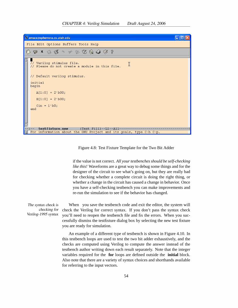
CHAPTER 4: Verilog Simulation Draft August 24, 2006
Figure 4.8: Test Fixture Template for the Two Bit Adder
if the value is not correct.All your testbenches should be self-checkinglike this! Waveforms are a great way to debug some things and for thedesigner of the circuit to see what’s going on, but they are really badfor checking whether a complete circuit is doing the right thing, orwhether a change in the circuit has caused a change in behavior. Onceyou have a self-checking testbench you can make improvements andre-run the simulation to see if the behavior has changed.
When you save the testbench code and exit the editor, the system willThe syntax check ischecking for
Verilog-1995 syntaxcheck the Verilog for correct syntax. If you don’t pass the syntax checkyou’ll need to reopen the testbench file and fix the errors. When you suc-cessfully dismiss the testfixture dialog box by selecting the new test fixtureyou are ready for simulation.
An example of a different type of testbench is shown in Figure 4.10. Inthis testbench loops are used to test the two bit adder exhaustively, and thechecks are computed using Verilog to compute the answer instead of thetestbench author writing down each result separately. Note that the integervariables required for thefor loops are defined outside theinitial block.Also note that there are a variety of syntax choices and shorthands availablefor referring to the input vectors.
54
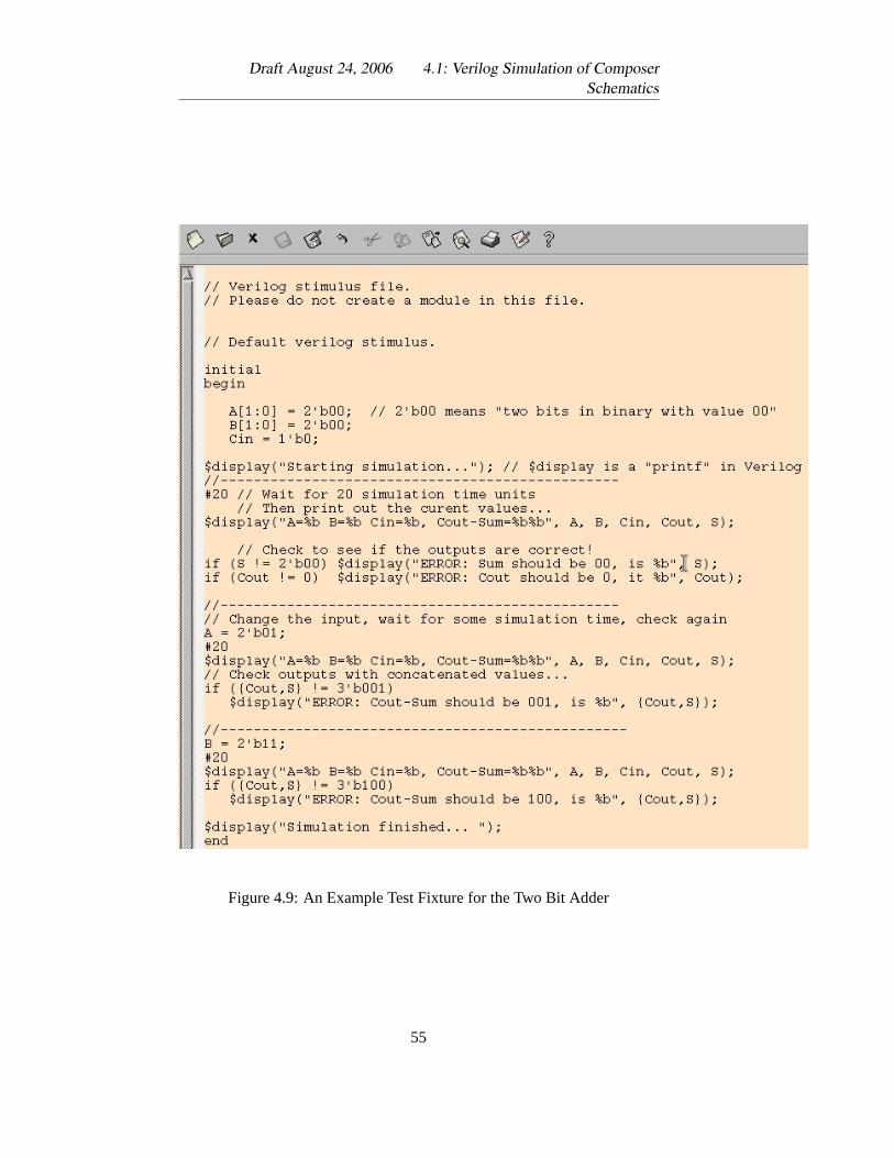
Draft August 24, 2006 4.1: Verilog Simulation of ComposerSchematics
Figure 4.9: An Example Test Fixture for the Two Bit Adder
55
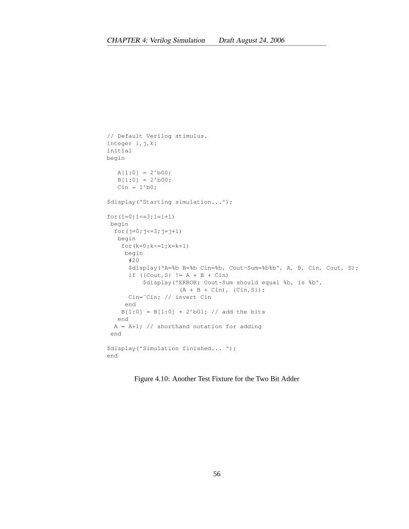
CHAPTER 4: Verilog Simulation Draft August 24, 2006
// Default Verilog stimulus.integer i,j,k;initialbegin
A[1:0] = 2’b00;B[1:0] = 2’b00;Cin = 1’b0;
$display("Starting simulation...");
for(i=0;i<=3;i=i+1)begin
for(j=0;j<=3;j=j+1)begin
for(k=0;k<=1;k=k+1)begin
#20$display("A=%b B=%b Cin=%b, Cout-Sum=%b%b", A, B, Cin, Cout, S);if ({Cout,S} != A + B + Cin)
$display("ERROR: Cout-Sum should equal %b, is %b",(A + B + Cin), {Cin,S});
Cin=˜Cin; // invert Cinend
B[1:0] = B[1:0] + 2’b01; // add the bitsend
A = A+1; // shorthand notation for addingend
$display("Simulation finished... ");end
Figure 4.10: Another Test Fixture for the Two Bit Adder
56
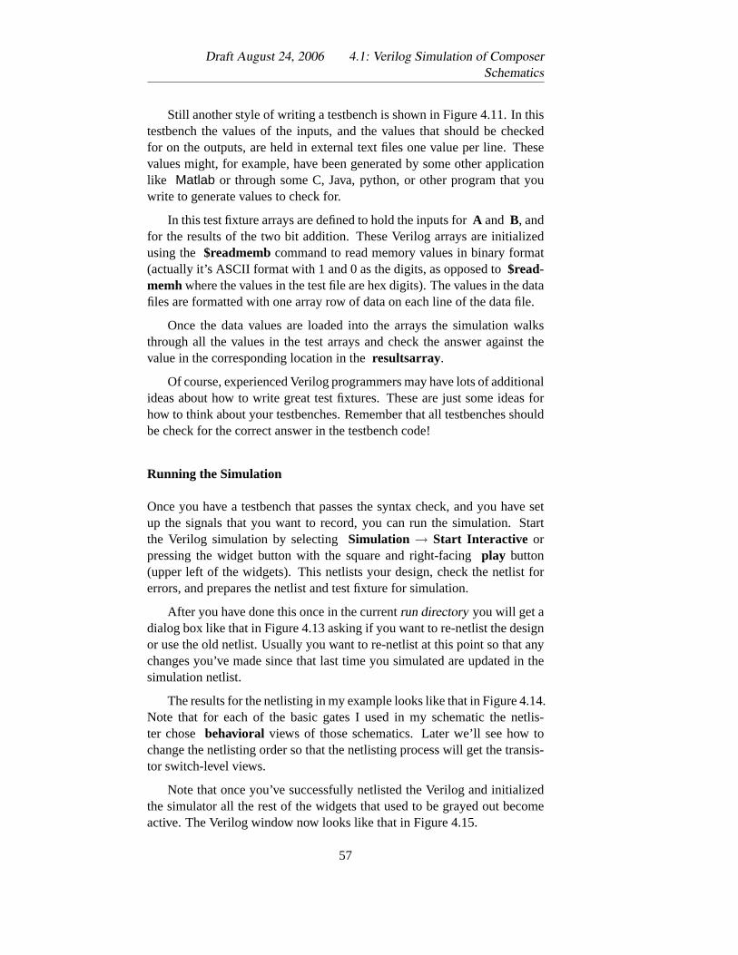
Draft August 24, 2006 4.1: Verilog Simulation of ComposerSchematics
Still another style of writing a testbench is shown in Figure 4.11. In thistestbench the values of the inputs, and the values that should be checkedfor on the outputs, are held in external text files one value per line. Thesevalues might, for example, have been generated by some other applicationlike Matlab or through some C, Java, python, or other program that youwrite to generate values to check for.
In this test fixture arrays are defined to hold the inputs forA and B, andfor the results of the two bit addition. These Verilog arrays are initializedusing the $readmembcommand to read memory values in binary format(actually it’s ASCII format with 1 and 0 as the digits, as opposed to$read-memhwhere the values in the test file are hex digits). The values in the datafiles are formatted with one array row of data on each line of the data file.
Once the data values are loaded into the arrays the simulation walksthrough all the values in the test arrays and check the answer against thevalue in the corresponding location in theresultsarray.
Of course, experienced Verilog programmers may have lots of additionalideas about how to write great test fixtures. These are just some ideas forhow to think about your testbenches. Remember that all testbenches shouldbe check for the correct answer in the testbench code!
Running the Simulation
Once you have a testbench that passes the syntax check, and you have setup the signals that you want to record, you can run the simulation. Startthe Verilog simulation by selectingSimulation → Start Interactive orpressing the widget button with the square and right-facingplay button(upper left of the widgets). This netlists your design, check the netlist forerrors, and prepares the netlist and test fixture for simulation.
After you have done this once in the currentrun directory you will get adialog box like that in Figure 4.13 asking if you want to re-netlist the designor use the old netlist. Usually you want to re-netlist at this point so that anychanges you’ve made since that last time you simulated are updated in thesimulation netlist.
The results for the netlisting in my example looks like that in Figure 4.14.Note that for each of the basic gates I used in my schematic the netlis-ter chose behavioral views of those schematics. Later we’ll see how tochange the netlisting order so that the netlisting process will get the transis-tor switch-level views.
Note that once you’ve successfully netlisted the Verilog and initializedthe simulator all the rest of the widgets that used to be grayed out becomeactive. The Verilog window now looks like that in Figure 4.15.
57
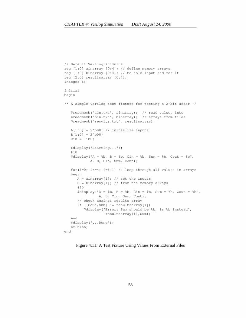
CHAPTER 4: Verilog Simulation Draft August 24, 2006
// Default Verilog stimulus.reg [1:0] ainarray [0:4]; // define memory arraysreg [1:0] binarray [0:4]; // to hold input and resultreg [2:0] resultsarray [0:4];integer i;
initialbegin
/* A simple Verilog test fixture for testing a 2-bit adder */
$readmemb("ain.txt", ainarray); // read values into$readmemb("bin.txt", binarray); // arrays from files$readmemb("results.txt", resultsarray);
A[1:0] = 2’b00; // initialize inputsB[1:0] = 2’b00;Cin = 1’b0;
$display("Starting...");#10$display("A = %b, B = %b, Cin = %b, Sum = %b, Cout = %b",
A, B, Cin, Sum, Cout);
for(i=0; i<=4; i=i+1) // loop through all values in arraysbegin
A = ainarray[i]; // set the inputsB = binarray[i]; // from the memory arrays#10$display("A = %b, B = %b, Cin = %b, Sum = %b, Cout = %b",
A, B, Cin, Sum, Cout);// check against results arrayif ({Cout,Sum} != resultsarray[i])
$display("Error: Sum should be %b, is %b instead",resultsarray[i],Sum);
end$display("...Done");$finish;
end
Figure 4.11: A Test Fixture Using Values From External Files
58
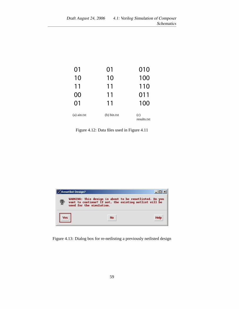
Draft August 24, 2006 4.1: Verilog Simulation of ComposerSchematics
(a) ain.txt (b) bin.txt (c)results.txt
Figure 4.12: Data files used in Figure 4.11
Figure 4.13: Dialog box for re-netlisting a previously netlisted design
59
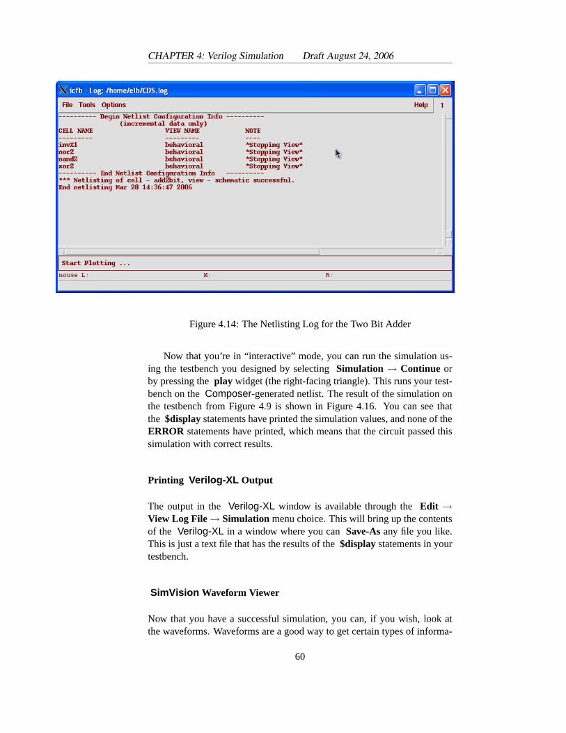
CHAPTER 4: Verilog Simulation Draft August 24, 2006
Figure 4.14: The Netlisting Log for the Two Bit Adder
Now that you’re in “interactive” mode, you can run the simulation us-ing the testbench you designed by selectingSimulation → Continue orby pressing theplay widget (the right-facing triangle). This runs your test-bench on theComposer-generated netlist. The result of the simulation onthe testbench from Figure 4.9 is shown in Figure 4.16. You can see thatthe $displaystatements have printed the simulation values, and none of theERROR statements have printed, which means that the circuit passed thissimulation with correct results.
Printing Verilog-XL Output
The output in the Verilog-XL window is available through theEdit →View Log File→ Simulation menu choice. This will bring up the contentsof the Verilog-XL in a window where you canSave-Asany file you like.This is just a text file that has the results of the$displaystatements in yourtestbench.
SimVision Waveform Viewer
Now that you have a successful simulation, you can, if you wish, look atthe waveforms. Waveforms are a good way to get certain types of informa-
60
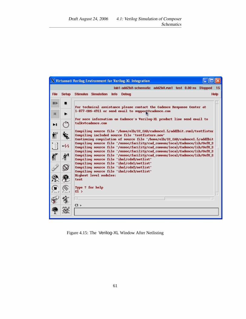
Draft August 24, 2006 4.1: Verilog Simulation of ComposerSchematics
Figure 4.15: TheVerilog-XL Window After Netlisting
61
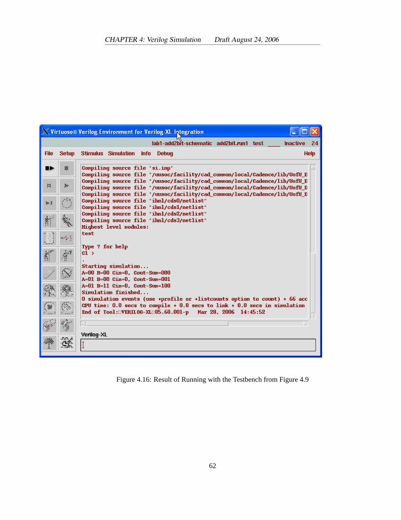
CHAPTER 4: Verilog Simulation Draft August 24, 2006
Figure 4.16: Result of Running with the Testbench from Figure 4.9
62
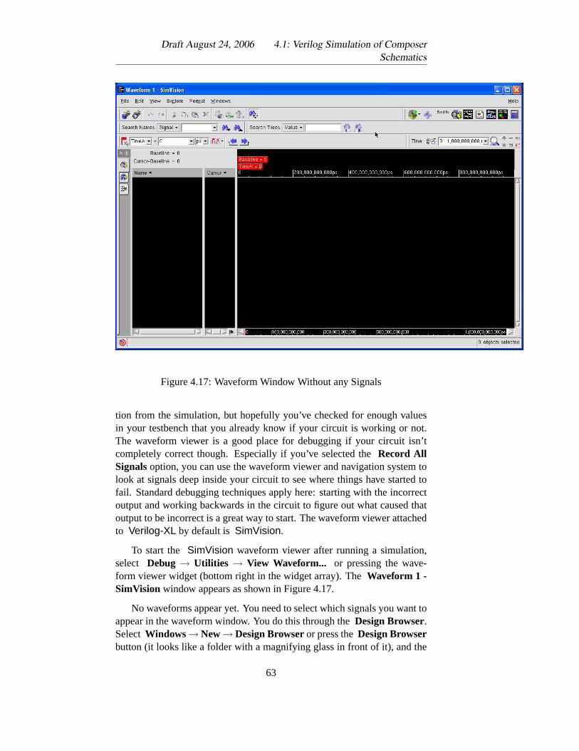
Draft August 24, 2006 4.1: Verilog Simulation of ComposerSchematics
Figure 4.17: Waveform Window Without any Signals
tion from the simulation, but hopefully you’ve checked for enough valuesin your testbench that you already know if your circuit is working or not.The waveform viewer is a good place for debugging if your circuit isn’tcompletely correct though. Especially if you’ve selected theRecord AllSignalsoption, you can use the waveform viewer and navigation system tolook at signals deep inside your circuit to see where things have started tofail. Standard debugging techniques apply here: starting with the incorrectoutput and working backwards in the circuit to figure out what caused thatoutput to be incorrect is a great way to start. The waveform viewer attachedto Verilog-XL by default is SimVision.
To start the SimVision waveform viewer after running a simulation,select Debug→ Utilities → View Waveform... or pressing the wave-form viewer widget (bottom right in the widget array). TheWaveform 1 -SimVision window appears as shown in Figure 4.17.
No waveforms appear yet. You need to select which signals you want toappear in the waveform window. You do this through theDesign Browser.SelectWindows→New→Design Browseror press theDesign Browserbutton (it looks like a folder with a magnifying glass in front of it), and the
63
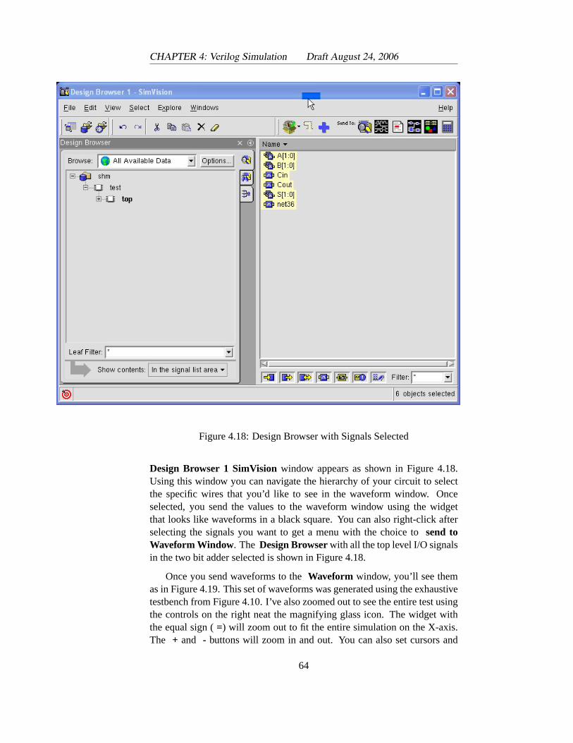
CHAPTER 4: Verilog Simulation Draft August 24, 2006
Figure 4.18: Design Browser with Signals Selected
Design Browser 1 SimVisionwindow appears as shown in Figure 4.18.Using this window you can navigate the hierarchy of your circuit to selectthe specific wires that you’d like to see in the waveform window. Onceselected, you send the values to the waveform window using the widgetthat looks like waveforms in a black square. You can also right-click afterselecting the signals you want to get a menu with the choice tosend toWaveform Window. The Design Browserwith all the top level I/O signalsin the two bit adder selected is shown in Figure 4.18.
Once you send waveforms to theWaveform window, you’ll see themas in Figure 4.19. This set of waveforms was generated using the exhaustivetestbench from Figure 4.10. I’ve also zoomed out to see the entire test usingthe controls on the right neat the magnifying glass icon. The widget withthe equal sign (=) will zoom out to fit the entire simulation on the X-axis.The + and - buttons will zoom in and out. You can also set cursors and
64
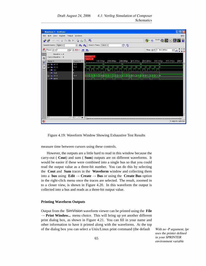
Draft August 24, 2006 4.1: Verilog Simulation of ComposerSchematics
Figure 4.19: Waveform Window Showing Exhaustive Test Results
measure time between cursors using these controls.
However, the outputs are a little hard to read in this window because thecarry-out (Cout) and sum (Sum) outputs are on different waveforms. Itwould be easier if these were combined into a single bus so that you couldread the output value as a three-bit number. You can do this by selectingthe Cout and Sum traces in theWaveform window and collecting theminto a bus using Edit → Create→ Bus or using theCreate Busoptionin the right-click menu once the traces are selected. The result, zoomed into a closer view, is shown in Figure 4.20. In this waveform the output iscollected into a bus and reads as a three-bit output value.
Printing Waveform Outputs
Output from theSimVision waveform viewer can be printed using theFile→ Print Window... menu choice. This will bring up yet another differentprint dialog box, as shown in Figure 4.21. You can fill in your name andother information to have it printed along with the waveforms. At the topof the dialog box you can select a Unix/Linux print command (the defaultWith no -P argument, lpr
uses the printer definedin your $PRINTERenvironment variable
65
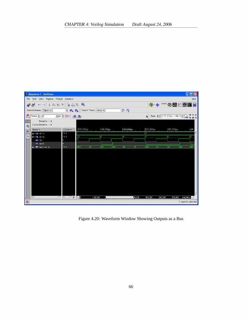
CHAPTER 4: Verilog Simulation Draft August 24, 2006
Figure 4.20: Waveform Window Showing Outputs as a Bus
66
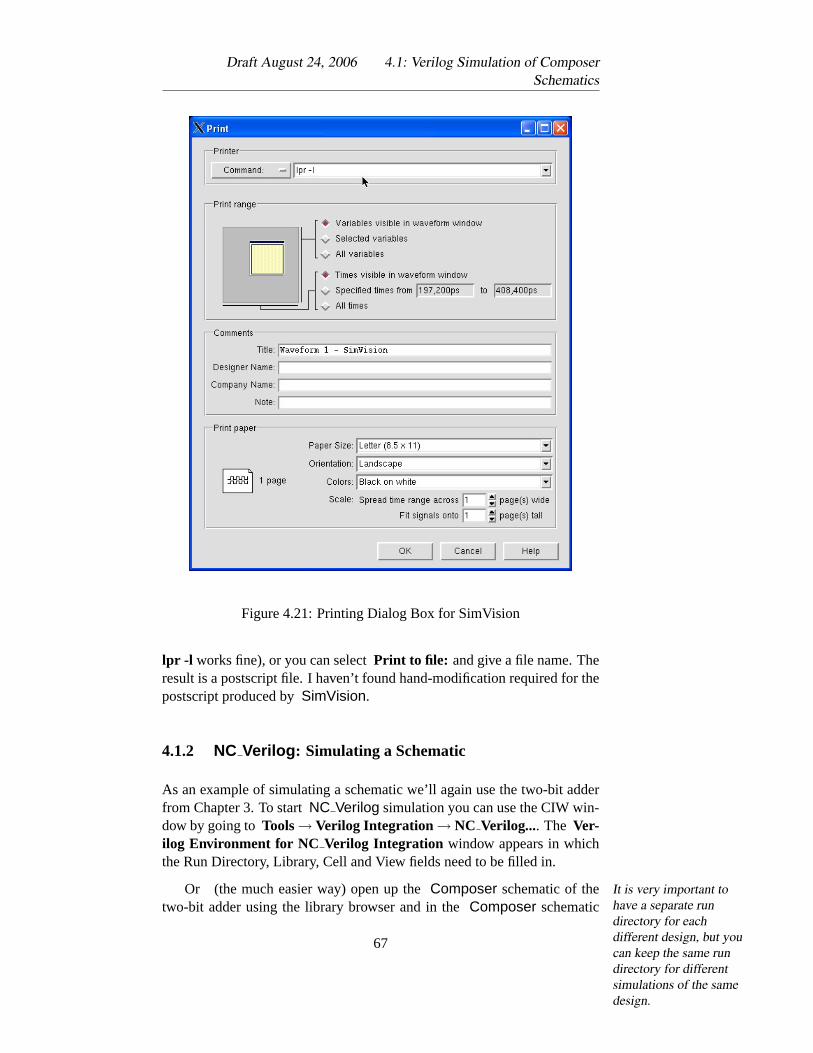
Draft August 24, 2006 4.1: Verilog Simulation of ComposerSchematics
Figure 4.21: Printing Dialog Box for SimVision
lpr -l works fine), or you can selectPrint to file: and give a file name. Theresult is a postscript file. I haven’t found hand-modification required for thepostscript produced bySimVision.
4.1.2 NC Verilog : Simulating a Schematic
As an example of simulating a schematic we’ll again use the two-bit adderfrom Chapter 3. To startNC Verilog simulation you can use the CIW win-dow by going toTools→ Verilog Integration → NC Verilog.... The Ver-ilog Environment for NC Verilog Integration window appears in whichthe Run Directory, Library, Cell and View fields need to be filled in.
Or (the much easier way) open up theComposer schematic of the It is very important tohave a separate rundirectory for eachdifferent design, but youcan keep the same rundirectory for differentsimulations of the samedesign.
two-bit adder using the library browser and in theComposer schematic
67
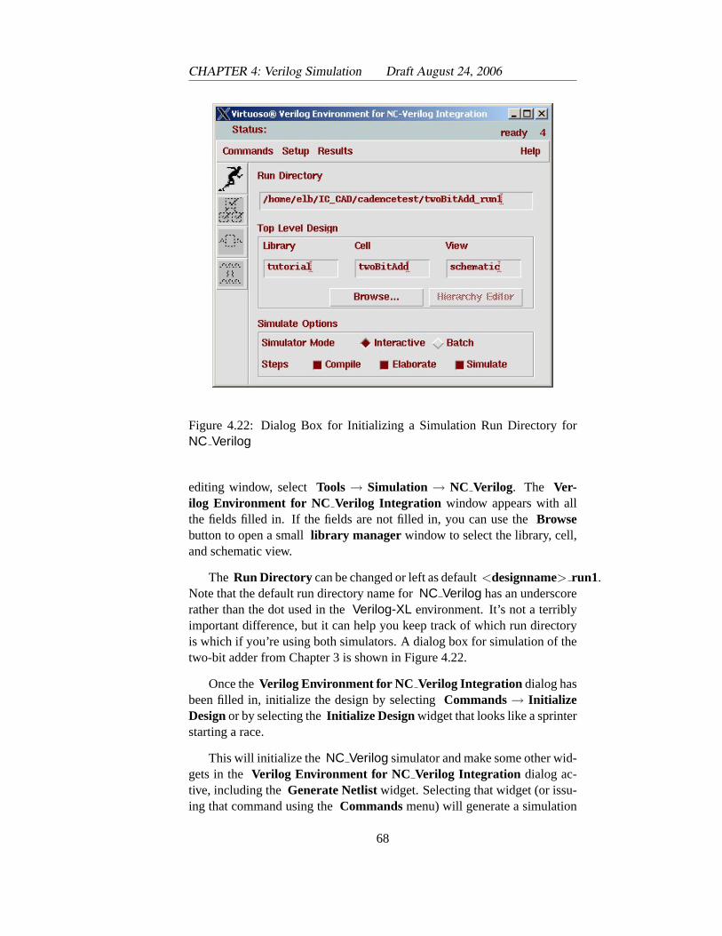
CHAPTER 4: Verilog Simulation Draft August 24, 2006
Figure 4.22: Dialog Box for Initializing a Simulation Run Directory forNC Verilog
editing window, selectTools → Simulation → NC Verilog. The Ver-ilog Environment for NC Verilog Integration window appears with allthe fields filled in. If the fields are not filled in, you can use theBrowsebutton to open a smalllibrary manager window to select the library, cell,and schematic view.
The Run Directory can be changed or left as default<designname> run1.Note that the default run directory name forNC Verilog has an underscorerather than the dot used in theVerilog-XL environment. It’s not a terriblyimportant difference, but it can help you keep track of which run directoryis which if you’re using both simulators. A dialog box for simulation of thetwo-bit adder from Chapter 3 is shown in Figure 4.22.
Once theVerilog Environment for NC Verilog Integration dialog hasbeen filled in, initialize the design by selectingCommands→ InitializeDesignor by selecting theInitialize Design widget that looks like a sprinterstarting a race.
This will initialize the NC Verilog simulator and make some other wid-gets in the Verilog Environment for NC Verilog Integration dialog ac-tive, including theGenerate Netlistwidget. Selecting that widget (or issu-ing that command using theCommandsmenu) will generate a simulation
68
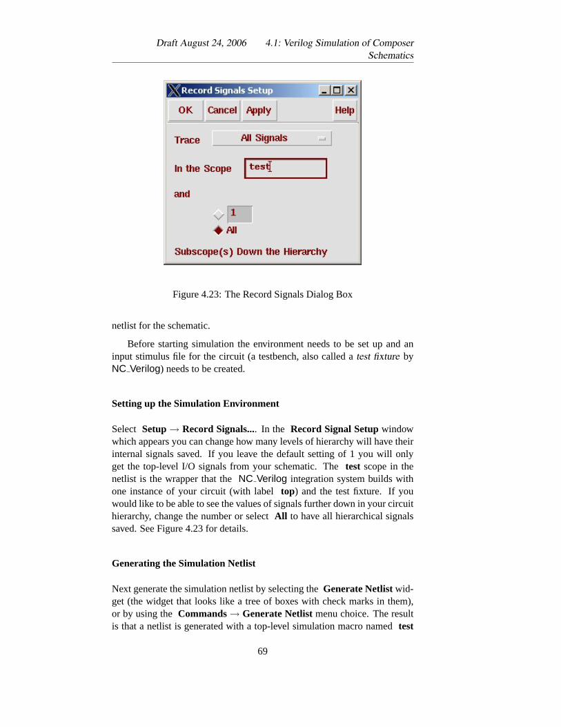
Draft August 24, 2006 4.1: Verilog Simulation of ComposerSchematics
Figure 4.23: The Record Signals Dialog Box
netlist for the schematic.
Before starting simulation the environment needs to be set up and aninput stimulus file for the circuit (a testbench, also called atest fixture byNC Verilog) needs to be created.
Setting up the Simulation Environment
Select Setup→ Record Signals.... In the Record Signal Setupwindowwhich appears you can change how many levels of hierarchy will have theirinternal signals saved. If you leave the default setting of 1 you will onlyget the top-level I/O signals from your schematic. Thetest scope in thenetlist is the wrapper that theNC Verilog integration system builds withone instance of your circuit (with labeltop) and the test fixture. If youwould like to be able to see the values of signals further down in your circuithierarchy, change the number or selectAll to have all hierarchical signalssaved. See Figure 4.23 for details.
Generating the Simulation Netlist
Next generate the simulation netlist by selecting theGenerate Netlistwid-get (the widget that looks like a tree of boxes with check marks in them),or by using theCommands→ Generate Netlistmenu choice. The resultis that a netlist is generated with a top-level simulation macro namedtest
69
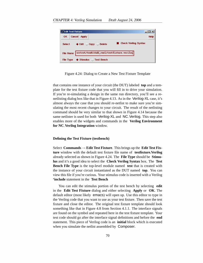
CHAPTER 4: Verilog Simulation Draft August 24, 2006
Figure 4.24: Dialog to Create a New Test Fixture Template
that contains one instance of your circuit (the DUT) labeledtop and a tem-plate for the test fixture code that you will fill in to drive your simulation.If you’re re-simulating a design in the same run directory, you’ll see a re-netlisting dialog box like that in Figure 4.13. As in theVerilog-XL case, it’salmost always the case that you should re-netlist to make sure you’re sim-ulating the most recent changes to your circuit. The result of the netlistingcommand should be very similar to that shown in Figure 4.14 because thesame netlister is used for bothVerilog-XL and NC Verilog. This step alsoenables more of the widgets and commands in theVerilog Environmentfor NC Verilog Integration window.
Defining the Test Fixture (testbench)
SelectCommands→ Edit Test Fixture . This brings up theEdit Test Fix-ture window with the default test fixture file name oftestfixture.Verilogalready selected as shown in Figure 4.24. TheFile Type should beStimu-lus and it’s a good idea to select theCheck Verilog Syntaxbox. The TestBench File Type is the top-level module namedtest that is created withthe instance of your circuit instantiated as the DUT namedtop. You canview this file if you’re curious. Your stimulus code is inserted with a Verilog‘include statement in theTest Bench
You can edit the stimulus portion of the test bench by selectingeditin the Edit Test Fixture dialog and either selectingApply or OK . Thedefault editor (most likelyemacs) will open up. Use this editor to type inthe Verilog code that you want to use as your test fixture. Then save the testfixture and close the editor. The original test fixture template should looksomething like that in Figure 4.8 from Section 4.1.1. The interface signalsare found on the symbol and repeated here in the test fixture template. Yourtest code should go after the interface signal definitions and before theendstatement. This piece of Verilog code is aninitial block which is executedwhen you simulate the netlist assembled byComposer.
70
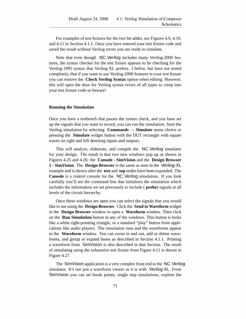
Draft August 24, 2006 4.1: Verilog Simulation of ComposerSchematics
For examples of test fixtures for the two bit adder, see Figures 4.9, 4.10,and 4.11 in Section 4.1.1. Once you have entered your test fixture code andsaved the result without Verilog errors you are ready to simulate.
Note that even thoughNC Verilog includes many Verilog-2000 fea-tures, the syntax checker for the test fixture appears to be checking for theVerilog-1995 syntax that Verilog-XL prefers. I belive, but have not testedcompletely, that if you want to use Verilog-2000 features in your test fixtureyou can remove theCheck Verilog Syntaxoption when editing. However,this will open the door for Verilog syntax errors of all types to creep intoyour test fixture code so beware!
Running the Simulation
Once you have a testbench that passes the syntax check, and you have setup the signals that you want to record, you can run the simulation. Start theVerilog simulation by selectingCommands→ Simulate menu choice orpressing theSimulate widget button with the DUT rectangle with squarewaves on right and left denoting inputs and outputs.
This will analyze, elaborate, and compile theNC Verilog simulatorfor your design. The result is that two new windows pop up as shown inFigures 4.25 and 4.26: theConsole - SimVisionand theDesign Browser1 - SimVision. The Design Browseris the same as seen in theVerilog-XLexample and is shown after thetestand top nodes have been expanded. TheConsoleis a control console for theNC Verilog simulation. If you lookcarefully you’ll see the command line that initializes the simulation whichincludes the information we set previously to include (probe) signals at alllevels of the circuit hierarchy.
Once these windows are open you can select the signals that you wouldlike to see using theDesign Browser. Click the Send to Waveformwidgetin the Design Browserwindow to open aWaveform window. Then clickon the Run Simulation button in any of the windows. This button is lookslike a white right-pointing triangle, or a standard “play” button from appli-cations like audio players. The simulation runs and the waveforms appearin the Waveform window. You can zoom in and out, add or delete wave-forms, and group or expand buses as described in Section 4.1.1. Printinga waveform from SimVision is also described in that Section. The resultof simulating using the exhaustive test fixture from Figure 4.11 is shown inFigure 4.27.
The SimVision application is a very complex front end to theNC Verilogsimulator. It’s not just a waveform viewer as it is withVerilog-XL. FromSimVision you can set break points, single step simulations, explore the
71
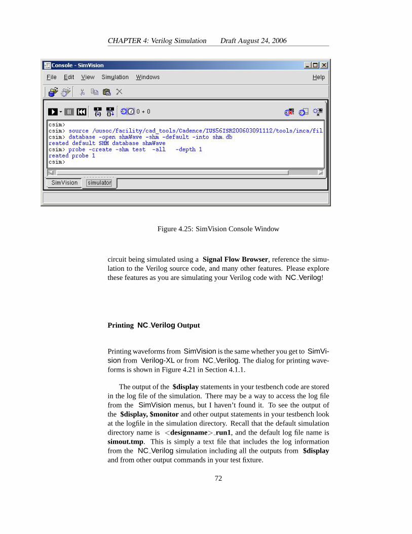
CHAPTER 4: Verilog Simulation Draft August 24, 2006
Figure 4.25: SimVision Console Window
circuit being simulated using aSignal Flow Browser, reference the simu-lation to the Verilog source code, and many other features. Please explorethese features as you are simulating your Verilog code withNC Verilog!
Printing NC Verilog Output
Printing waveforms fromSimVision is the same whether you get toSimVi-sion from Verilog-XL or from NC Verilog. The dialog for printing wave-forms is shown in Figure 4.21 in Section 4.1.1.
The output of the$displaystatements in your testbench code are storedin the log file of the simulation. There may be a way to access the log filefrom the SimVision menus, but I haven’t found it. To see the output ofthe $display, $monitor and other output statements in your testbench lookat the logfile in the simulation directory. Recall that the default simulationdirectory name is<designname> run1, and the default log file name issimout.tmp. This is simply a text file that includes the log informationfrom the NC Verilog simulation including all the outputs from$displayand from other output commands in your test fixture.
72
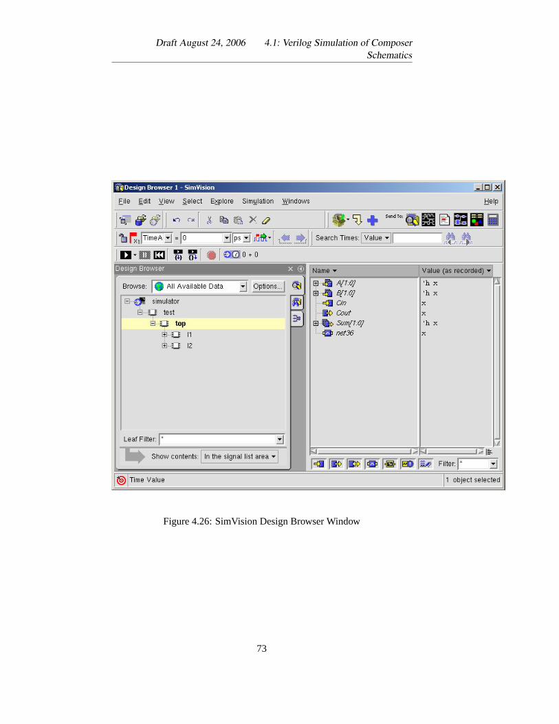
Draft August 24, 2006 4.1: Verilog Simulation of ComposerSchematics
Figure 4.26: SimVision Design Browser Window
73
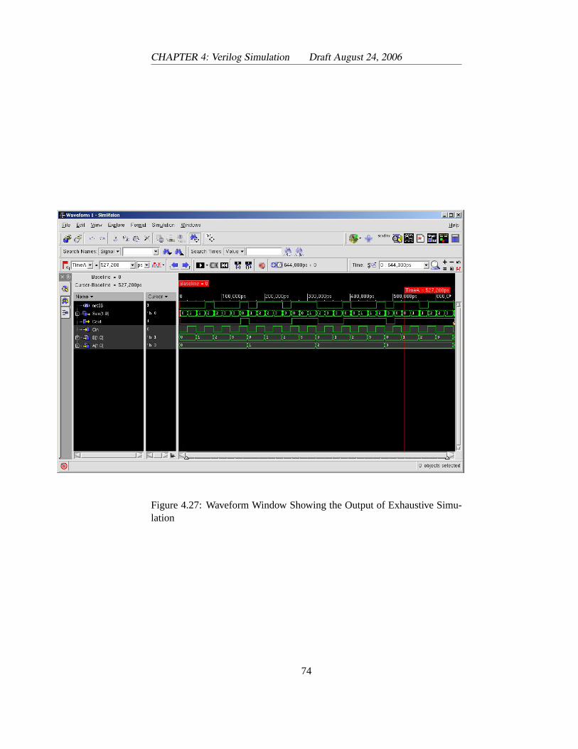
CHAPTER 4: Verilog Simulation Draft August 24, 2006
Figure 4.27: Waveform Window Showing the Output of Exhaustive Simu-lation
74
Draft August 24, 2006 4.2: Behavioral Verilog Code in Composer
4.2 Behavioral Verilog Code in Composer
One way to describe the functionality of your circuit is to use collections ofBoolean gates from a standard cell library, as is shown in the previous sec-tions. Another way is to describe the functionality of the circuit as Verilogcode. The Verilog code might be purely structural meaning that it consistsonly of instantiations of gates from that same standard cell library. In thatcase the Verilog is simply a textual version of the schematic. Verilog canalso describe a circuit as a behavior meaning that it uses statements in theVerilog language to describe the desired behavior. A behavioral Verilog de-scription will look much more like a software program than like a circuitSynthesis of behavioral
Verilog into structural(gate-level) Verilog iscovered in Chapter 8.
description, and will need to be converted (orsynthesized) into a structuraldescription at some point if you want to actually build the circuit, but as aninitial description, a behavioral model can be much more compact, can usehigher-level descriptions, and can simulate much more quickly.
A behavioral Verilog model can be developed as a Verilog program us-ing a text editor, and simulated using a Verilog simulator without ever usingthe Composer schematic tool as will be seen in Section 4.3. However,symbols in Composer schematics can be an interface to behavioral Ver-ilog code just as easily as they can contain gate schematics. These symbolswhich encapsulate Verilog behavioral code may be connected in schematicsusing wires just like other symbols, and can peacefully coexist with othersymbols that encapsulate gate views. The cell view used for generalNote that cell views that
consist of transistors orthat correspond to asingle standard cell mayuse cmos sch as theirschematic view
schematics isschematicand the cell view we use for behavioral Verilogviews is behavioral. In fact, a single cell may have both of these views andyou can tell the netlister later which view to use in a given simulation. Youcan actually use any view name you like for the Verilog behavioral view.It might actually make sense in some situations to use a different name,like verilog for your Verilog view so you can keep track of which pieces ofVerilog are your own behavioral code and which pieces of Verilog are thelibrary cell descriptions. For now we won’t make a distinction.
This allows great freedom in terms of how you want to describe yourcircuits. You can start with a Verilogbehavioral view for initial functionalsimulation, and then incrementally refine pieces of the circuit into gate levelschematicviews, all while using the same testbench code for simulation.
4.2.1 Generating a Behavioral View
Making a behavioral view is very similar to making any other cell view. Youuse the Library Manager to make a new cell view, except that you choosebehavioral as the view name instead ofschematic.
Start in the Library Manager and select the library in which you want to
75
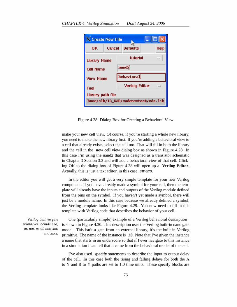
CHAPTER 4: Verilog Simulation Draft August 24, 2006
Figure 4.28: Dialog Box for Creating a Behavioral View
make your new cell view. Of course, if you’re starting a whole new library,you need to make the new library first. If you’re adding a behavioral view toa cell that already exists, select the cell too. That will fill in both the libraryand the cell in thenew cell viewdialog box as shown in Figure 4.28. Inthis case I’m using the nand2 that was designed as a transistor schematicin Chapter 3 Section 3.3 and will add a behavioral view of that cell. Click-ing OK to the dialog box of Figure 4.28 will open up aVerilog Editor .Actually, this is just a text editor, in this caseemacs.
In the editor you will get a very simple template for your new Verilogcomponent. If you have already made a symbol for your cell, then the tem-plate will already have the inputs and outputs of the Verilog module definedfrom the pins on the symbol. If you haven’t yet made a symbol, there willjust be a module name. In this case because we already defined a symbol,the Verilog template looks like Figure 4.29. You now need to fill in thistemplate with Verilog code that describes the behavior of your cell.
One (particularly simple) example of a Verilog behavioral descriptionVerilog built-in gateprimitives include and,or, not, nand, nor, xor,
and xnor.
is shown in Figure 4.30. This description uses the Verilog built-in nand gatemodel. This isn’t a gate from an external library, it’s the built-in Verilogprimitive. The name of the instance isi0. Note that I’ve given the instancea name that starts in an underscore so that if I ever navigate to this instancein a simulation I can tell that it came from the behavioral model of the cell.
I’ve also usedspecifystatements to describe the input to output delayof the cell. In this case both the rising and falling delays for both the Ato Y and B to Y paths are set to 1.0 time units. These specify blocks are
76
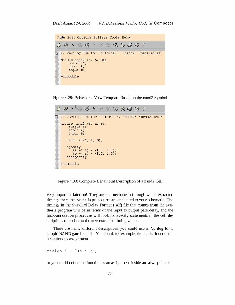
Draft August 24, 2006 4.2: Behavioral Verilog Code in Composer
Figure 4.29: Behavioral View Template Based on the nand2 Symbol
Figure 4.30: Complete Behavioral Description of a nand2 Cell
very important later on! They are the mechanism through which extractedtimings from the synthesis procedures are annotated to your schematic. Thetimings in the Standard Delay Format (.sdf) file that comes from the syn-thesis program will be in terms of the input to output path delay, and theback-annotation procedure will look for specify statements in the cell de-scriptions to update to the new extracted timing values.
There are many different descriptions you could use in Verilog for asimple NAND gate like this. You could, for example, define the function asa continuous assignment
assign Y = ˜(A & B);
or you could define the function as an assignment inside analwaysblock
77
CHAPTER 4: Verilog Simulation Draft August 24, 2006
reg Y;always @(A or B)
beginY = ˜(A & B);
end
or, if you had a standard cell library available with the appropriate gates,you could define it the NAND as a structural composition of gates from thatlibrary.
wire w;AND2 _u1(w, A, B);INV _u2(Y,w);
Each of these descriptions would work. The point is that any legal Ver-ilog behavioral/structural syntax that will simulate in the Verilog simulatorwill work for the contents of abehavioral cell view.
Once you have entered your Verilog code into the template in the editor,save the file and quit the editor. This will cause theComposer VerilogThe syntax checker
appears to be checkingfor Verilog 1995 (i.e.
Verilog-XL) syntax inthis check.
integration system to check the syntax of your code and make sure that itis compatible with the Verilog editor. If it reports errors you need to re-editand fix your Verilog code.
It will also check to make sure that the pin descriptions in your schematicview, the pins in your symbol, and the interface in your behavioral view areall consistent. This is critical if all the different views can be used in variouscombinations in later simulations.
Once you have a behavioral view of a cell, that view can be simu-lated from Composer using a Cadence Verilog simulator, and it canbe included via the symbol in other schematics and those schematics canbe simulated using eitherVerilog-XL or NC Verilog. All of the cells inthe UofU Digital v1 1 library have behavioral views. These views are thedefault choice when simulating schematics that include instances of thesecells. If a transistor switch-level simulation is desired, follow the procedurein Section 4.4.1.
4.2.2 Simulating a Behavioral View
The simplest way to simulate a behavioral view is to make a new schematicand include an instance of the symbol that encapsulates the behavioral view.Then you can use the procedure described in Section 4.1.1 to simulate withVerilog-XL, or the procedure described in Section 4.1.2 to simulate withNC Verilog.
78
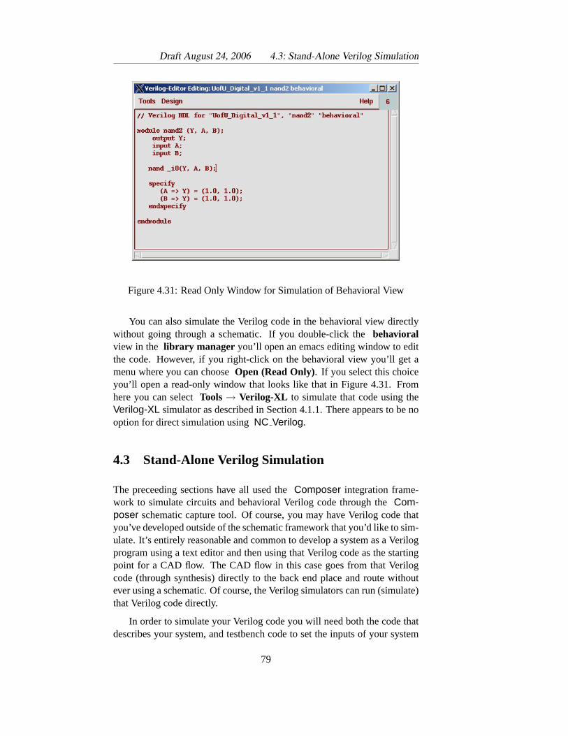
Draft August 24, 2006 4.3: Stand-Alone Verilog Simulation
Figure 4.31: Read Only Window for Simulation of Behavioral View
You can also simulate the Verilog code in the behavioral view directlywithout going through a schematic. If you double-click thebehavioralview in the library manager you’ll open an emacs editing window to editthe code. However, if you right-click on the behavioral view you’ll get amenu where you can chooseOpen (Read Only). If you select this choiceyou’ll open a read-only window that looks like that in Figure 4.31. Fromhere you can selectTools→ Verilog-XL to simulate that code using theVerilog-XL simulator as described in Section 4.1.1. There appears to be nooption for direct simulation usingNC Verilog.
4.3 Stand-Alone Verilog Simulation
The preceeding sections have all used theComposer integration frame-work to simulate circuits and behavioral Verilog code through theCom-poser schematic capture tool. Of course, you may have Verilog code thatyou’ve developed outside of the schematic framework that you’d like to sim-ulate. It’s entirely reasonable and common to develop a system as a Verilogprogram using a text editor and then using that Verilog code as the startingpoint for a CAD flow. The CAD flow in this case goes from that Verilogcode (through synthesis) directly to the back end place and route withoutever using a schematic. Of course, the Verilog simulators can run (simulate)that Verilog code directly.
In order to simulate your Verilog code you will need both the code thatdescribes your system, and testbench code to set the inputs of your system
79
CHAPTER 4: Verilog Simulation Draft August 24, 2006
and check that the outputs are correct. As shown in Figure 4.1 this corre-sponds to DUT code (the code describing your system) and testbench ortestfixture code. These should both be part of a single top-level module thatis simulated. An example is shown in Figure 4.2 where the testfixture codeis contained in a separate file namedtestfixture.verilog.
As another example, consider the Verilog code describing a simple statemachine shown in Figure 4.32. This state machine looks at bits on the inputinsig and raises the output signalsaw4whenever the last four bits have allbeen 1. Of course, there are simpler ways of building a circuit with thisfunctionality, but it makes a perfectly good example of a small finite statemachine to simulate with each of the Verilog simulators.
In order to simulate this piece of Verilog code a testbench is required.Based on the technique described in Figures 4.1 and 4.2, a top-level Verilogfile is required that includes an instance of thesee4module and some test-bench code. This top-level file is shown in Figure 4.33, and an example of apossible testbench in thetestfixture.v included file is shown in Figure 4.34.These files will be used to demonstrate each of the Verilog simulators instand-alone mode.
4.3.1 Verilog-XL
Verilog-XL is an interpreted Verilog simulator from Cadence that is the ref-erence simulator for the Verilog-1995 standard. This means that Verilogconstructs from later versions of the standard will not run with this simu-lator. As seen in Section 4.1.1, it is well-integrated with theComposerschematic capture system, but it is easily used on its own too. The inputs tothe simulator are, at the simplest, just a list of the Verilog files to simulate,but can also include a dizzying array of additional arguments and switchesto control the behavior of the simulator. If you’re already set your path toinclude the standard CAD scripts (see Section 2.2), then you can invoke theVerilog-XL simulator using the script
sim-xl <verilogfilename >
I find it useful to put the files that you want to simulate in a separate file,and then invoke the simulator with the -f switch to point to that file. In thecase of our example from Figures 4.32 to 4.34, thefiles.txt file simply liststhe see4.v and seetest.v files and looks like:
see4.vseetest.v
In this case, I would invoke theVerilog-XL simulator using the com-mand:
80
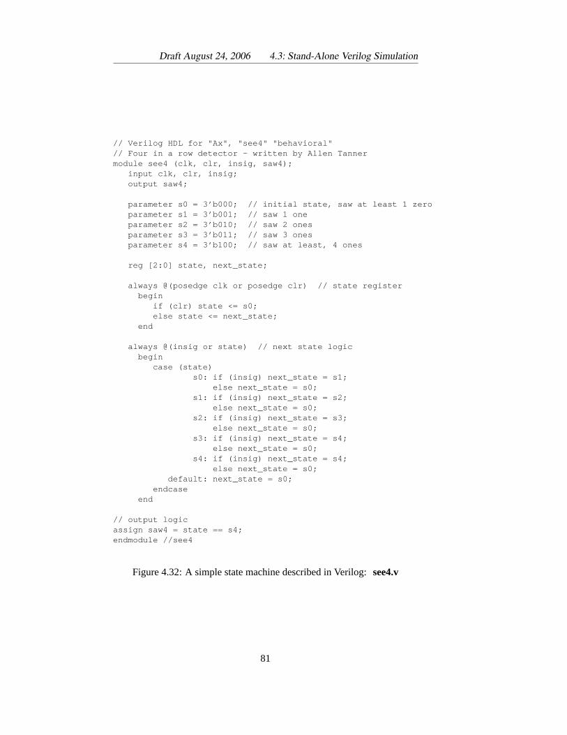
Draft August 24, 2006 4.3: Stand-Alone Verilog Simulation
// Verilog HDL for "Ax", "see4" "behavioral"// Four in a row detector - written by Allen Tannermodule see4 (clk, clr, insig, saw4);
input clk, clr, insig;output saw4;
parameter s0 = 3’b000; // initial state, saw at least 1 zeroparameter s1 = 3’b001; // saw 1 oneparameter s2 = 3’b010; // saw 2 onesparameter s3 = 3’b011; // saw 3 onesparameter s4 = 3’b100; // saw at least, 4 ones
reg [2:0] state, next_state;
always @(posedge clk or posedge clr) // state registerbegin
if (clr) state <= s0;else state <= next_state;
end
always @(insig or state) // next state logicbegin
case (state)s0: if (insig) next_state = s1;
else next_state = s0;s1: if (insig) next_state = s2;
else next_state = s0;s2: if (insig) next_state = s3;
else next_state = s0;s3: if (insig) next_state = s4;
else next_state = s0;s4: if (insig) next_state = s4;
else next_state = s0;default: next_state = s0;
endcaseend
// output logicassign saw4 = state == s4;endmodule //see4
Figure 4.32: A simple state machine described in Verilog:see4.v
81
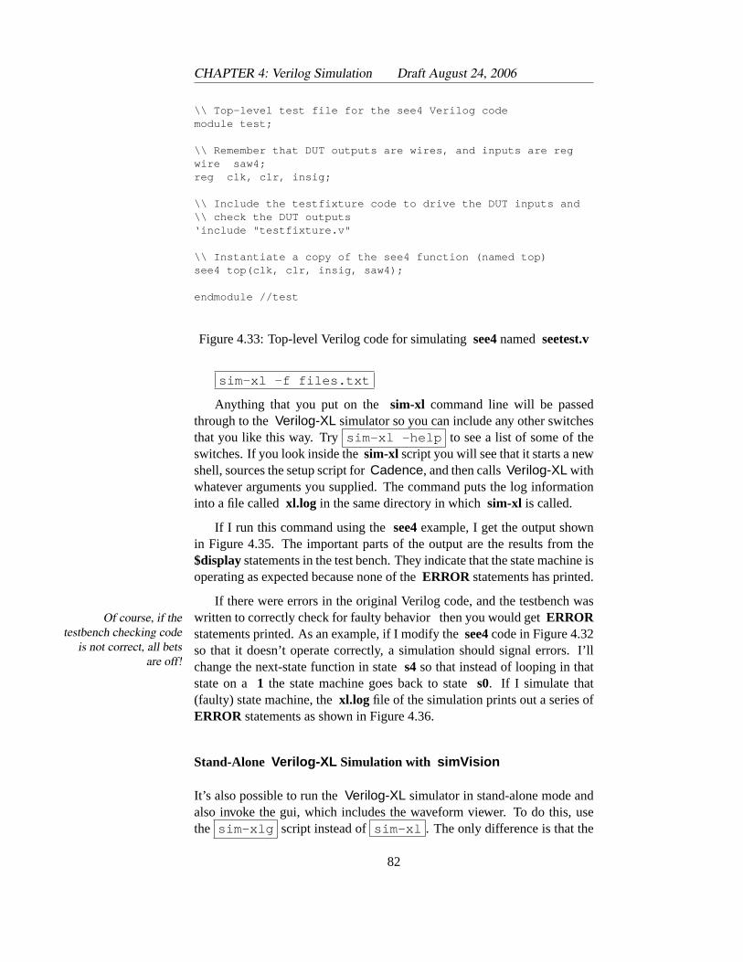
CHAPTER 4: Verilog Simulation Draft August 24, 2006
\\ Top-level test file for the see4 Verilog codemodule test;
\\ Remember that DUT outputs are wires, and inputs are regwire saw4;reg clk, clr, insig;
\\ Include the testfixture code to drive the DUT inputs and\\ check the DUT outputs‘include "testfixture.v"
\\ Instantiate a copy of the see4 function (named top)see4 top(clk, clr, insig, saw4);
endmodule //test
Figure 4.33: Top-level Verilog code for simulatingsee4namedseetest.v
sim-xl -f files.txt
Anything that you put on thesim-xl command line will be passedthrough to theVerilog-XL simulator so you can include any other switchesthat you like this way. Trysim-xl -help to see a list of some of theswitches. If you look inside thesim-xl script you will see that it starts a newshell, sources the setup script forCadence, and then callsVerilog-XL withwhatever arguments you supplied. The command puts the log informationinto a file calledxl.log in the same directory in whichsim-xl is called.
If I run this command using thesee4example, I get the output shownin Figure 4.35. The important parts of the output are the results from the$displaystatements in the test bench. They indicate that the state machine isoperating as expected because none of theERROR statements has printed.
If there were errors in the original Verilog code, and the testbench waswritten to correctly check for faulty behavior then you would getERROROf course, if the
testbench checking codeis not correct, all bets
are off!
statements printed. As an example, if I modify thesee4code in Figure 4.32so that it doesn’t operate correctly, a simulation should signal errors. I’llchange the next-state function in states4so that instead of looping in thatstate on a 1 the state machine goes back to states0. If I simulate that(faulty) state machine, thexl.log file of the simulation prints out a series ofERROR statements as shown in Figure 4.36.
Stand-Alone Verilog-XL Simulation with simVision
It’s also possible to run theVerilog-XL simulator in stand-alone mode andalso invoke the gui, which includes the waveform viewer. To do this, usethe sim-xlg script instead ofsim-xl . The only difference is that the
82
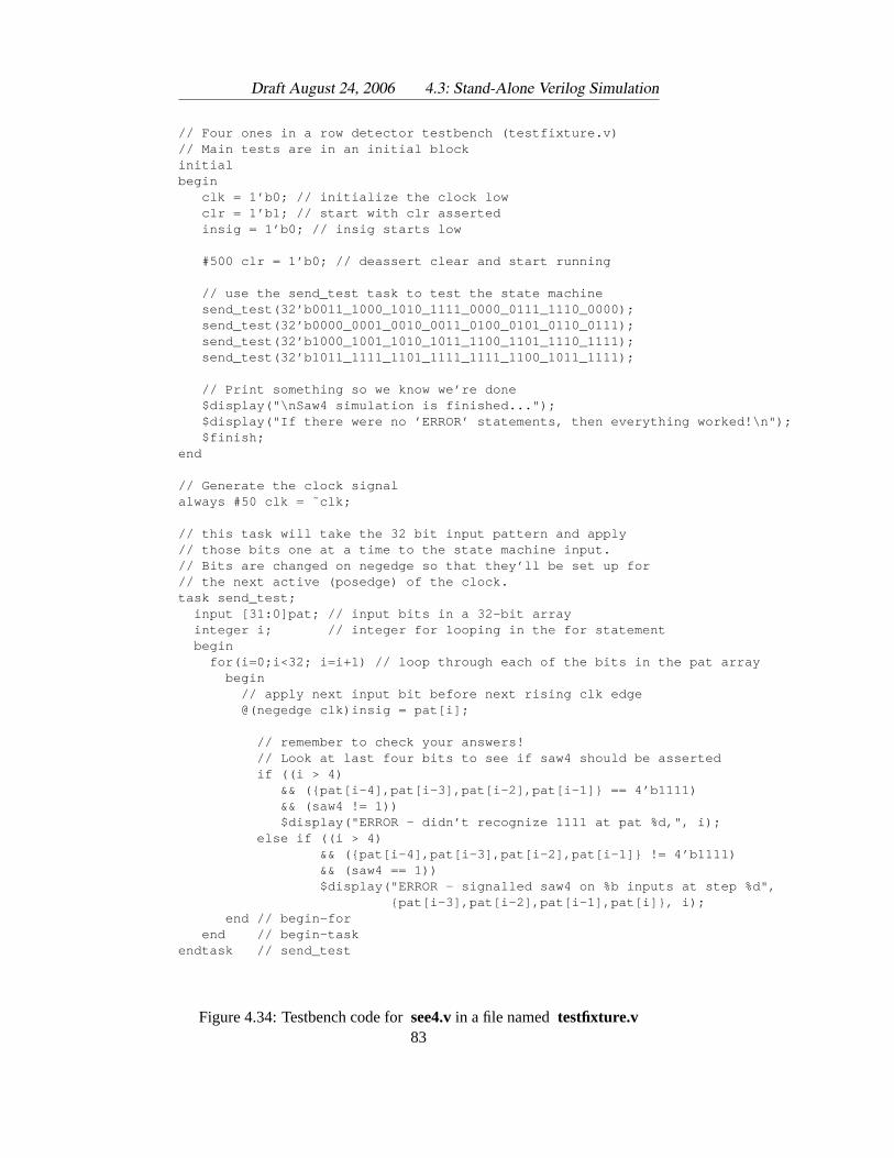
Draft August 24, 2006 4.3: Stand-Alone Verilog Simulation
// Four ones in a row detector testbench (testfixture.v)// Main tests are in an initial blockinitialbegin
clk = 1’b0; // initialize the clock lowclr = 1’b1; // start with clr assertedinsig = 1’b0; // insig starts low
#500 clr = 1’b0; // deassert clear and start running
// use the send_test task to test the state machinesend_test(32’b0011_1000_1010_1111_0000_0111_1110_0000);send_test(32’b0000_0001_0010_0011_0100_0101_0110_0111);send_test(32’b1000_1001_1010_1011_1100_1101_1110_1111);send_test(32’b1011_1111_1101_1111_1111_1100_1011_1111);
// Print something so we know we’re done$display("\nSaw4 simulation is finished...");$display("If there were no ’ERROR’ statements, then everything worked!\n");$finish;
end
// Generate the clock signalalways #50 clk = ˜clk;
// this task will take the 32 bit input pattern and apply// those bits one at a time to the state machine input.// Bits are changed on negedge so that they’ll be set up for// the next active (posedge) of the clock.task send_test;
input [31:0]pat; // input bits in a 32-bit arrayinteger i; // integer for looping in the for statementbegin
for(i=0;i<32; i=i+1) // loop through each of the bits in the pat arraybegin
// apply next input bit before next rising clk edge@(negedge clk)insig = pat[i];
// remember to check your answers!// Look at last four bits to see if saw4 should be assertedif ((i > 4)
&& ({pat[i-4],pat[i-3],pat[i-2],pat[i-1]} == 4’b1111)&& (saw4 != 1))$display("ERROR - didn’t recognize 1111 at pat %d,", i);
else if ((i > 4)&& ({pat[i-4],pat[i-3],pat[i-2],pat[i-1]} != 4’b1111)&& (saw4 == 1))$display("ERROR - signalled saw4 on %b inputs at step %d",
{pat[i-3],pat[i-2],pat[i-1],pat[i]}, i);end // begin-for
end // begin-taskendtask // send_test
Figure 4.34: Testbench code forsee4.vin a file namedtestfixture.v83
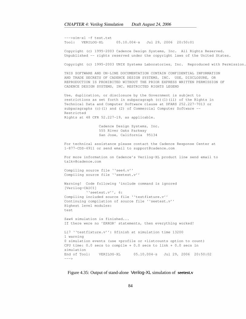
CHAPTER 4: Verilog Simulation Draft August 24, 2006
--->sim-xl -f test.txtTool: VERILOG-XL 05.10.004-s Jul 29, 2006 20:50:01
Copyright (c) 1995-2003 Cadence Design Systems, Inc. All Rights Reserved.Unpublished -- rights reserved under the copyright laws of the United States.
Copyright (c) 1995-2003 UNIX Systems Laboratories, Inc. Reproduced with Permission.
THIS SOFTWARE AND ON-LINE DOCUMENTATION CONTAIN CONFIDENTIAL INFORMATIONAND TRADE SECRETS OF CADENCE DESIGN SYSTEMS, INC. USE, DISCLOSURE, ORREPRODUCTION IS PROHIBITED WITHOUT THE PRIOR EXPRESS WRITTEN PERMISSION OFCADENCE DESIGN SYSTEMS, INC. RESTRICTED RIGHTS LEGEND
Use, duplication, or disclosure by the Government is subject torestrictions as set forth in subparagraph (c)(1)(ii) of the Rights inTechnical Data and Computer Software clause at DFARS 252.227-7013 orsubparagraphs (c)(1) and (2) of Commercial Computer Software --RestrictedRights at 48 CFR 52.227-19, as applicable.
Cadence Design Systems, Inc.555 River Oaks ParkwaySan Jose, California 95134
For technical assistance please contact the Cadence Response Center at1-877-CDS-4911 or send email to [email protected]
For more information on Cadence’s Verilog-XL product line send email [email protected]
Compiling source file ‘‘see4.v’’Compiling source file ‘‘seetest.v’’
Warning! Code following ‘include command is ignored[Verilog-CAICI]
‘‘seetest.v’’, 6:Compiling included source file ‘‘testfixture.v’’Continuing compilation of source file ‘‘seetest.v’’Highest level modules:test
Saw4 simulation is finished...If there were no ’ERROR’ statements, then everything worked!
L17 ‘‘testfixture.v’’: $finish at simulation time 132001 warning0 simulation events (use +profile or +listcounts option to count)CPU time: 0.0 secs to compile + 0.0 secs to link + 0.0 secs insimulationEnd of Tool: VERILOG-XL 05.10.004-s Jul 29, 2006 20:50:02--->
Figure 4.35: Output of stand-aloneVerilog-XL simulation of seetest.v
84
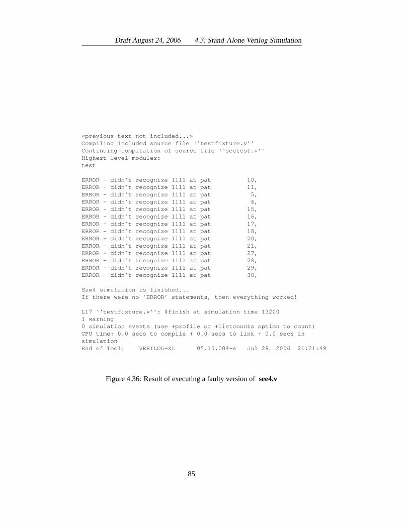
Draft August 24, 2006 4.3: Stand-Alone Verilog Simulation
<previous text not included...>Compiling included source file ‘‘testfixture.v’’Continuing compilation of source file ‘‘seetest.v’’Highest level modules:test
ERROR - didn’t recognize 1111 at pat 10,ERROR - didn’t recognize 1111 at pat 11,ERROR - didn’t recognize 1111 at pat 5,ERROR - didn’t recognize 1111 at pat 6,ERROR - didn’t recognize 1111 at pat 15,ERROR - didn’t recognize 1111 at pat 16,ERROR - didn’t recognize 1111 at pat 17,ERROR - didn’t recognize 1111 at pat 18,ERROR - didn’t recognize 1111 at pat 20,ERROR - didn’t recognize 1111 at pat 21,ERROR - didn’t recognize 1111 at pat 27,ERROR - didn’t recognize 1111 at pat 28,ERROR - didn’t recognize 1111 at pat 29,ERROR - didn’t recognize 1111 at pat 30,
Saw4 simulation is finished...If there were no ’ERROR’ statements, then everything worked!
L17 ‘‘testfixture.v’’: $finish at simulation time 132001 warning0 simulation events (use +profile or +listcounts option to count)CPU time: 0.0 secs to compile + 0.0 secs to link + 0.0 secs insimulationEnd of Tool: VERILOG-XL 05.10.004-s Jul 29, 2006 21:21:49
Figure 4.36: Result of executing a faulty version ofsee4.v
85
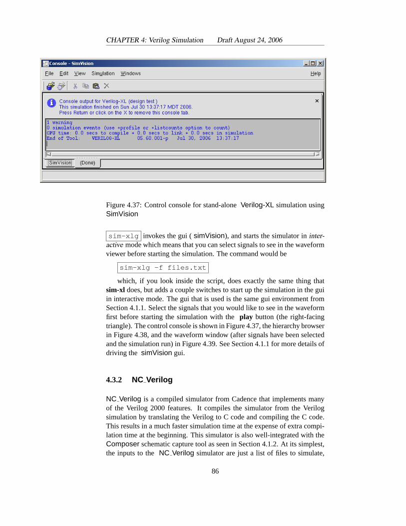
CHAPTER 4: Verilog Simulation Draft August 24, 2006
Figure 4.37: Control console for stand-aloneVerilog-XL simulation usingSimVision
sim-xlg invokes the gui (simVision), and starts the simulator ininter-active mode which means that you can select signals to see in the waveformviewer before starting the simulation. The command would be
sim-xlg -f files.txt
which, if you look inside the script, does exactly the same thing thatsim-xl does, but adds a couple switches to start up the simulation in the guiin interactive mode. The gui that is used is the same gui environment fromSection 4.1.1. Select the signals that you would like to see in the waveformfirst before starting the simulation with theplay button (the right-facingtriangle). The control console is shown in Figure 4.37, the hierarchy browserin Figure 4.38, and the waveform window (after signals have been selectedand the simulation run) in Figure 4.39. See Section 4.1.1 for more details ofdriving the simVision gui.
4.3.2 NC Verilog
NC Verilog is a compiled simulator from Cadence that implements manyof the Verilog 2000 features. It compiles the simulator from the Verilogsimulation by translating the Verilog to C code and compiling the C code.This results in a much faster simulation time at the expense of extra compi-lation time at the beginning. This simulator is also well-integrated with theComposer schematic capture tool as seen in Section 4.1.2. At its simplest,the inputs to theNC Verilog simulator are just a list of files to simulate,
86
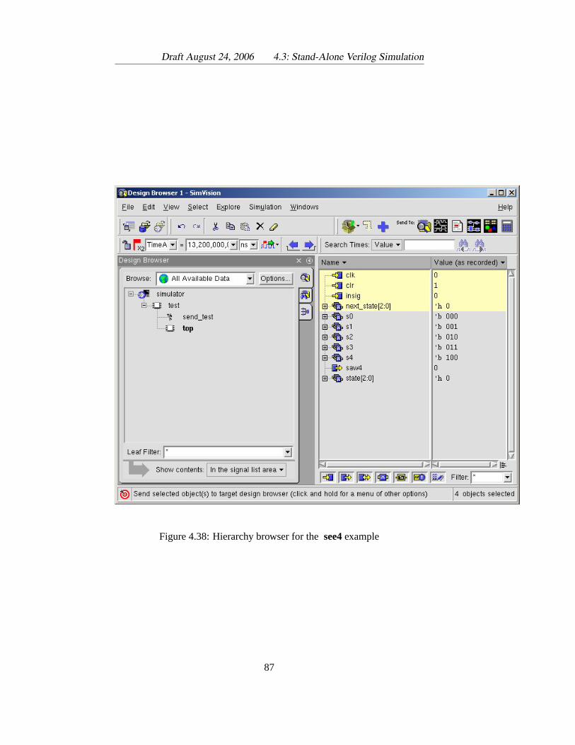
Draft August 24, 2006 4.3: Stand-Alone Verilog Simulation
Figure 4.38: Hierarchy browser for thesee4example
87
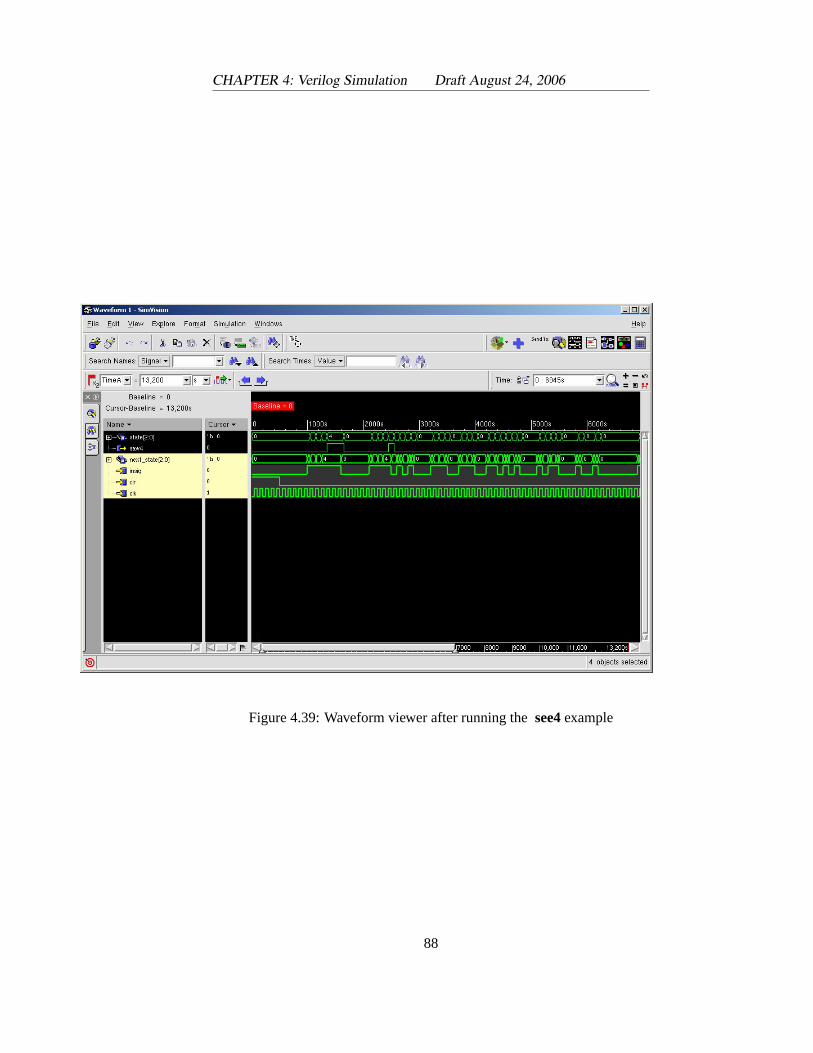
CHAPTER 4: Verilog Simulation Draft August 24, 2006
Figure 4.39: Waveform viewer after running thesee4example
88

Draft August 24, 2006 4.3: Stand-Alone Verilog Simulation
but like other Verilog simulators, there are many many switches that can begiven at the command line to control the simulation. If you’re already setyour path to include the standard CAD scripts (see Section 2.2), then youcan invoke theNC Verilog simulator using the script
sim-nc <verilogfilename >
I find it useful to put the files that you want to simulate in a separate file,and then invoke the simulator with the -f switch to point to that file. In thecase of our example from Figures 4.32 to 4.34, thefiles.txt file simply liststhe see4.v and seetest.v files and looks like:
see4.vseetest.v
In this case, I would invoke theNC Verilog simulator using the com-mand:
sim-nc -f files.txt
Anything that you put on thesim-nc command line will be passedthrough to theNC Verilog simulator so you can include any other switchesthat you like this way. Trysim-nc -help to see a list of some of theswitches. If you look inside thesim-nc script you will see that it starts anew shell, sources the setup script forCadence, and then callsNC Verilogwith the command line information that you have supplied. The log file isnc.log. If I run this command using thesee4example, I get the outputshown in Figure 4.40. The important parts of the output are the results fromthe $display statements in the test bench. They indicate that the state ma-chine is operating as expected because none of theERROR statements hasprinted.
If there were errors in the original Verilog code, and the testbench waswritten to correctly check for faulty behavior then you would getERROR Of course, if the
testbench checking codeis not correct, all betsare off!
statements printed. These error statements would look similar to those inFigure 4.36.
Stand-Alone NC Verilog Simulation with simVision
It’s also possible to run theNC Verilog simulator in stand-alone mode andalso invoke the gui, which includes the waveform viewer. To do this, usethe sim-ncg script instead ofsim-nc . The only difference is that the
sim-ncg invokes the gui (simVision), and starts the simulator ininter-active mode which means that you can select signals to see in the waveformviewer before starting the simulation. The command would be
89
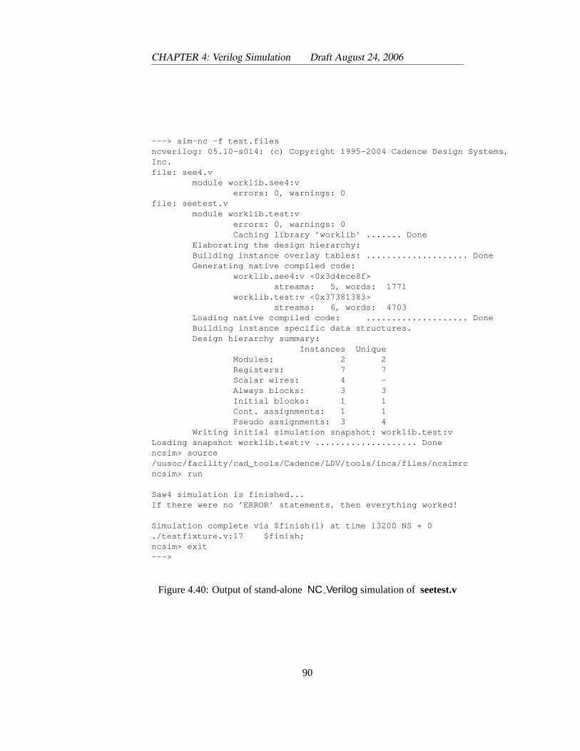
CHAPTER 4: Verilog Simulation Draft August 24, 2006
---> sim-nc -f test.filesncverilog: 05.10-s014: (c) Copyright 1995-2004 Cadence Design Systems,Inc.file: see4.v
module worklib.see4:verrors: 0, warnings: 0
file: seetest.vmodule worklib.test:v
errors: 0, warnings: 0Caching library ’worklib’ ....... Done
Elaborating the design hierarchy:Building instance overlay tables: .................... DoneGenerating native compiled code:
worklib.see4:v <0x3d4ece8f>streams: 5, words: 1771
worklib.test:v <0x37381383>streams: 6, words: 4703
Loading native compiled code: .................... DoneBuilding instance specific data structures.Design hierarchy summary:
Instances UniqueModules: 2 2Registers: 7 7Scalar wires: 4 -Always blocks: 3 3Initial blocks: 1 1Cont. assignments: 1 1Pseudo assignments: 3 4
Writing initial simulation snapshot: worklib.test:vLoading snapshot worklib.test:v .................... Donencsim> source/uusoc/facility/cad_tools/Cadence/LDV/tools/inca/files/ncsimrcncsim> run
Saw4 simulation is finished...If there were no ’ERROR’ statements, then everything worked!
Simulation complete via $finish(1) at time 13200 NS + 0./testfixture.v:17 $finish;ncsim> exit--->
Figure 4.40: Output of stand-aloneNC Verilog simulation of seetest.v
90
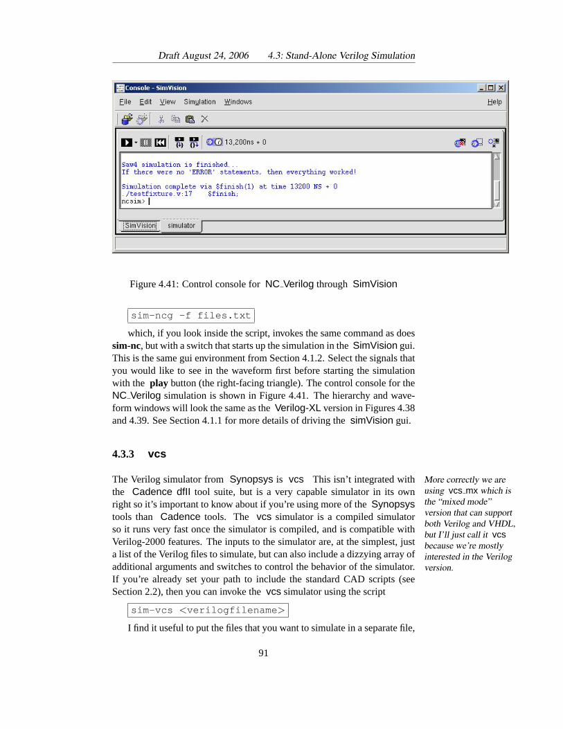
Draft August 24, 2006 4.3: Stand-Alone Verilog Simulation
Figure 4.41: Control console forNC Verilog through SimVision
sim-ncg -f files.txt
which, if you look inside the script, invokes the same command as doessim-nc, but with a switch that starts up the simulation in theSimVision gui.This is the same gui environment from Section 4.1.2. Select the signals thatyou would like to see in the waveform first before starting the simulationwith the play button (the right-facing triangle). The control console for theNC Verilog simulation is shown in Figure 4.41. The hierarchy and wave-form windows will look the same as theVerilog-XL version in Figures 4.38and 4.39. See Section 4.1.1 for more details of driving thesimVision gui.
4.3.3 vcs
The Verilog simulator fromSynopsys is vcs This isn’t integrated with More correctly we areusing vcs mx which isthe “mixed mode”version that can supportboth Verilog and VHDL,but I’ll just call it vcsbecause we’re mostlyinterested in the Verilogversion.
the Cadence dfII tool suite, but is a very capable simulator in its ownright so it’s important to know about if you’re using more of theSynopsystools than Cadence tools. The vcs simulator is a compiled simulatorso it runs very fast once the simulator is compiled, and is compatible withVerilog-2000 features. The inputs to the simulator are, at the simplest, justa list of the Verilog files to simulate, but can also include a dizzying array ofadditional arguments and switches to control the behavior of the simulator.If you’re already set your path to include the standard CAD scripts (seeSection 2.2), then you can invoke thevcs simulator using the script
sim-vcs <verilogfilename >
I find it useful to put the files that you want to simulate in a separate file,
91
CHAPTER 4: Verilog Simulation Draft August 24, 2006
and then invoke the simulator with the -f switch to point to that file. In thecase of our example from Figures 4.32 to 4.34, thefiles.txt file simply liststhe see4.v and seetest.v files and looks like:
see4.vseetest.v
In this case, I would invoke thevcs simulator using the command:
sim-vcs -f files.txt
Anything that you put on thesim-vcs command line will be passedthrough to the vcs simulator so you can include any other switches thatyou like this way. Try sim-vcs -help to see a list of some of theswitches. If you look inside thesim-vcsscript you will see that it starts anew shell, sources the setup script forSynopsys, and then callsvcs withthe command line information you have supplied. The log file isvcs.log.If I run this command using thesee4example, I get the output shown inFigure 4.42.
For the vcs simulator, running thesim-vcsscript doesn’t actually runthe simulation. Instead it compiles the Verilog code into an executable calledsimv. After compiling this simulator, you can run it by runningsimv toget the output seen in Figure 4.43, but thesimv executable needs somesetup information aboutSynopsys before it can run, so rather than runsimv directly, you will run it through a wrapper calledsim-simvas follows:
sim-simv <executable-name >
Because the executable will be namedsimv unless you’ve overriddenthat default name with a command-line switch, this will almost always becalled as:
sim-simv simv
The important parts of the output are the results from the$displaystate-ments in the test bench. They indicate that the state machine is operating asexpected because none of theERROR statements has printed.
If there were errors in the original Verilog code, and the testbench waswritten to correctly check for faulty behavior then you would getERROROf course, if the
testbench checking codeis not correct, all bets
are off!
statements printed. These error statements would look similar to those inFigure 4.36.
Stand-Alone vcs Simulation with VirSim
It’s also possible to run thevcs simulator in stand-alone mode and alsoinvoke the gui, which includes the waveform viewer. To do this, use the
92
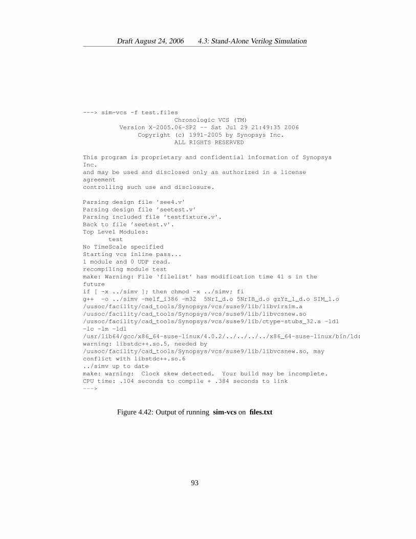
Draft August 24, 2006 4.3: Stand-Alone Verilog Simulation
---> sim-vcs -f test.filesChronologic VCS (TM)
Version X-2005.06-SP2 -- Sat Jul 29 21:49:35 2006Copyright (c) 1991-2005 by Synopsys Inc.
ALL RIGHTS RESERVED
This program is proprietary and confidential information of SynopsysInc.and may be used and disclosed only as authorized in a licenseagreementcontrolling such use and disclosure.
Parsing design file ’see4.v’Parsing design file ’seetest.v’Parsing included file ’testfixture.v’.Back to file ’seetest.v’.Top Level Modules:
testNo TimeScale specifiedStarting vcs inline pass...1 module and 0 UDP read.recompiling module testmake: Warning: File ‘filelist’ has modification time 41 s in thefutureif [ -x ../simv ]; then chmod -x ../simv; fig++ -o ../simv -melf_i386 -m32 5NrI_d.o 5NrIB_d.o gzYz_1_d.o SIM_l.o/uusoc/facility/cad_tools/Synopsys/vcs/suse9/lib/libvirsim.a/uusoc/facility/cad_tools/Synopsys/vcs/suse9/lib/libvcsnew.so/uusoc/facility/cad_tools/Synopsys/vcs/suse9/lib/ctype-stubs_32.a -ldl-lc -lm -ldl/usr/lib64/gcc/x86_64-suse-linux/4.0.2/../../../../x86_64-suse-linux/bin/ld:warning: libstdc++.so.5, needed by/uusoc/facility/cad_tools/Synopsys/vcs/suse9/lib/libvcsnew.so, mayconflict with libstdc++.so.6../simv up to datemake: warning: Clock skew detected. Your build may be incomplete.CPU time: .104 seconds to compile + .384 seconds to link--->
Figure 4.42: Output of runningsim-vcson files.txt
93
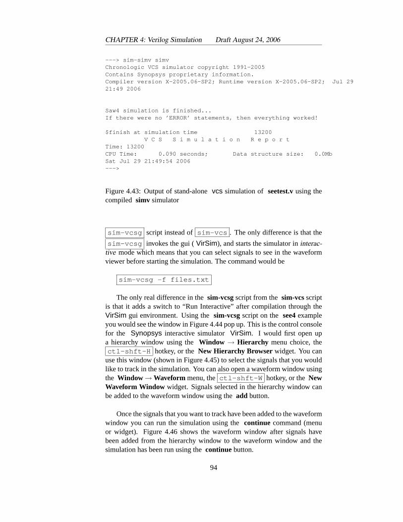
CHAPTER 4: Verilog Simulation Draft August 24, 2006
---> sim-simv simvChronologic VCS simulator copyright 1991-2005Contains Synopsys proprietary information.Compiler version X-2005.06-SP2; Runtime version X-2005.06-SP2; Jul 2921:49 2006
Saw4 simulation is finished...If there were no ’ERROR’ statements, then everything worked!
$finish at simulation time 13200V C S S i m u l a t i o n R e p o r t
Time: 13200CPU Time: 0.090 seconds; Data structure size: 0.0MbSat Jul 29 21:49:54 2006--->
Figure 4.43: Output of stand-alonevcs simulation of seetest.vusing thecompiled simv simulator
sim-vcsg script instead ofsim-vcs . The only difference is that the
sim-vcsg invokes the gui (VirSim), and starts the simulator ininterac-tive mode which means that you can select signals to see in the waveformviewer before starting the simulation. The command would be
sim-vcsg -f files.txt
The only real difference in thesim-vcsgscript from thesim-vcsscriptis that it adds a switch to “Run Interactive” after compilation through theVirSim gui environment. Using thesim-vcsgscript on the see4exampleyou would see the window in Figure 4.44 pop up. This is the control consolefor the Synopsys interactive simulator VirSim. I would first open upa hierarchy window using theWindow → Hierarchy menu choice, thectl-shft-H hotkey, or theNew Hierarchy Browser widget. You can
use this window (shown in Figure 4.45) to select the signals that you wouldlike to track in the simulation. You can also open a waveform window usingthe Window →Waveform menu, thectl-shft-W hotkey, or theNewWaveform Window widget. Signals selected in the hierarchy window canbe added to the waveform window using theadd button.
Once the signals that you want to track have been added to the waveformwindow you can run the simulation using thecontinue command (menuor widget). Figure 4.46 shows the waveform window after signals havebeen added from the hierarchy window to the waveform window and thesimulation has been run using thecontinuebutton.
94
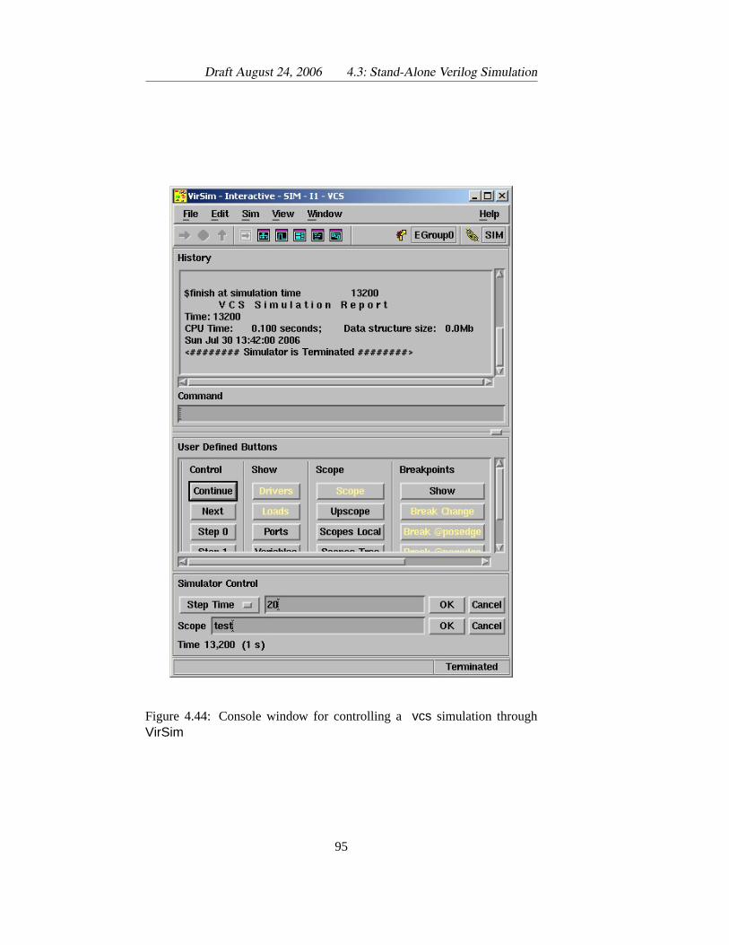
Draft August 24, 2006 4.3: Stand-Alone Verilog Simulation
Figure 4.44: Console window for controlling avcs simulation throughVirSim
95
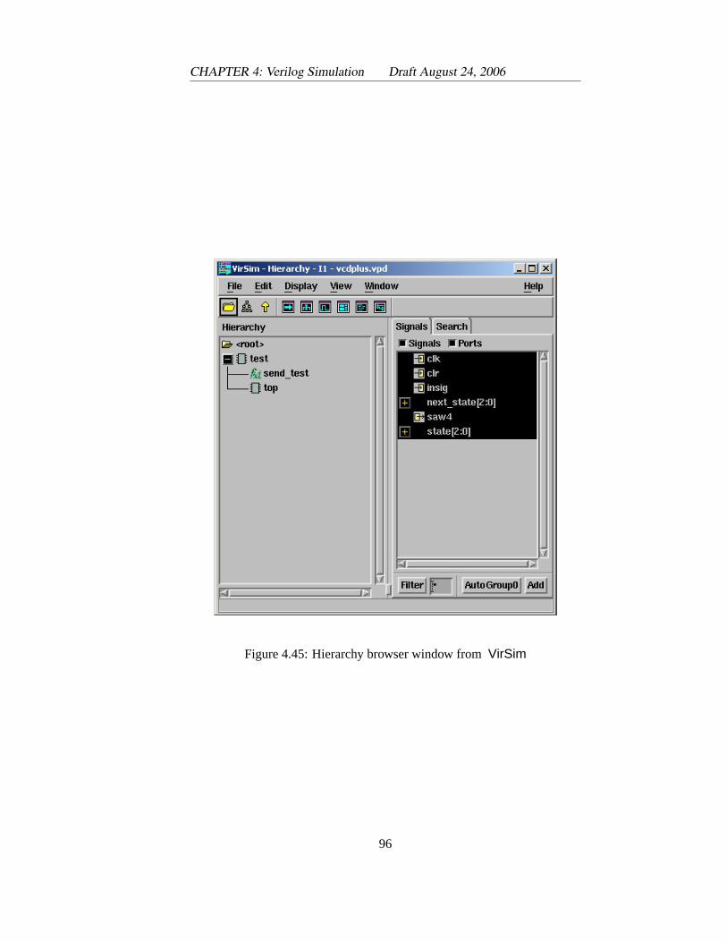
CHAPTER 4: Verilog Simulation Draft August 24, 2006
Figure 4.45: Hierarchy browser window fromVirSim
96
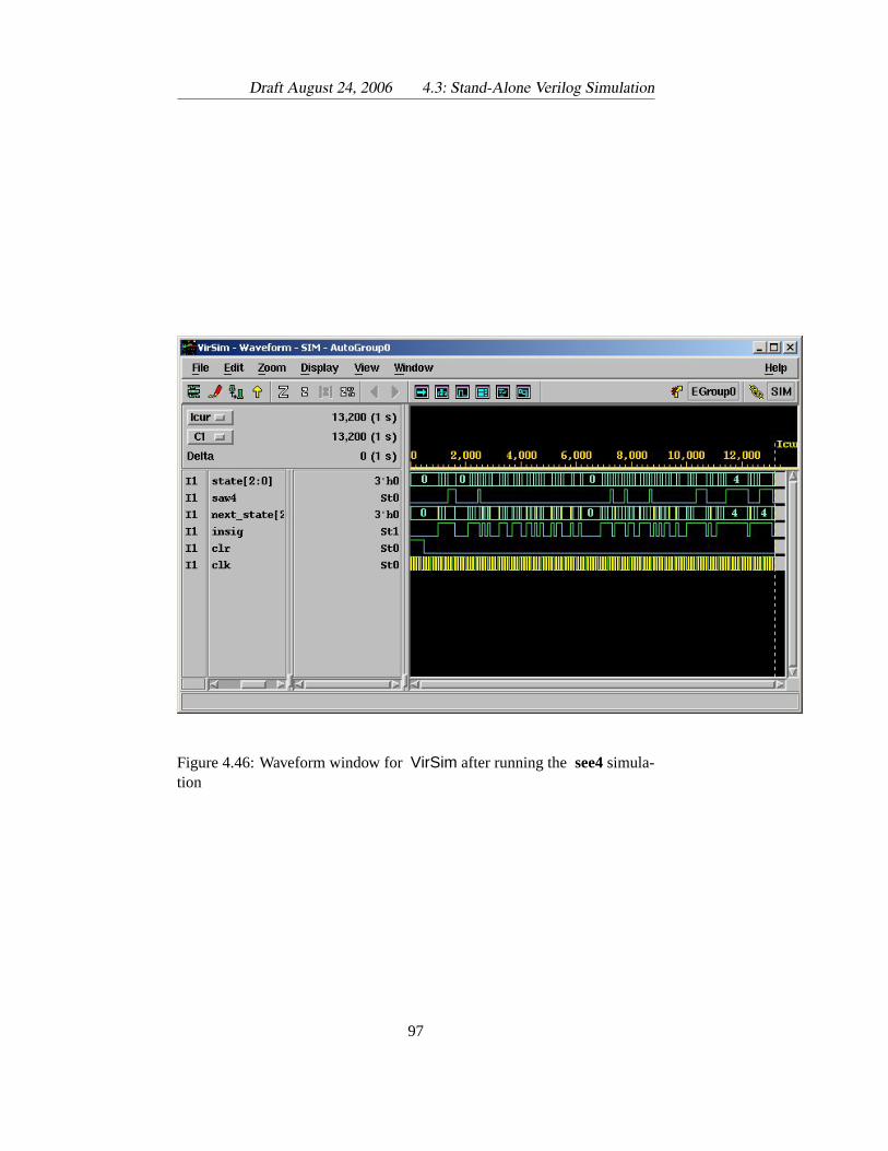
Draft August 24, 2006 4.3: Stand-Alone Verilog Simulation
Figure 4.46: Waveform window forVirSim after running thesee4simula-tion
97
CHAPTER 4: Verilog Simulation Draft August 24, 2006
4.4 Timing in Verilog Simulations
Time is modeled in a Verilog simulation either by explicit delay statementsor through implicit constructs that wait for an event or an edge of a signal be-fore progressing. Explicit delays are denoted with the# character. You’veseen the# character used in the testbench code examples in this chapter.The simplest syntax is#10which means to delay 10 time units before pro-ceeding with the simulation and executing the following statement. You canalso use the#8:10:12syntax to indicate minimum, typical, and maximumdelays. If delays are specified in this way you can choose which delay to usein a given simulation using command-line switches to the Verilog simulator.Typically (and for the three simulators we use) this is accomplished with a+mindelays, +typdelaysor +maxdelayscommand-line argument.
Of course, if the#10construct delays by 10 time units, it is importantto know if those time units correspond to any real time units or are simplyunit delay timings that are not meant to model any specific real time values.Verilog uses the ‘timescale command to specify the connection betweentiming units and real timing numbers. The‘timescaledirective takes twoarguments: a timing unit and a timing precision. For example,
‘timescale 1 ns / 100 ps
means that each “unit” corresponds to 1ns, and the precision at whichtimings are computed is 100ps. But be careful! For many simulations thedelay numbers donot correspond to actual real times and are simply generic“unit timings” to model the fact that time passes without trying to model theexact amount of time the activity takes. Make sure you understand howtiming is used in your simulation before you make assumptions!
Implicit delays in a Verilog simulation are signaled using the@ char-acter which causes the following statement or procedural block to wait forsome event before proceeding. The even might be a signal transition on awire, an edge (posedgeor negedge) of a signal change, or an abstracteventthrough the Verilogeventconstruct. These implicit delays are often used,for example, to wait for an active clock edge before proceeding.
4.4.1 Behavioral versus Transistor Switch Simulation
In our CAD flow there are two main types of Verilog simulations:
Behavioral: The Verilog describes the desired behavior of the system inhigh-level terms. This description does not correspond directly tohardware, but can be synthesized into hardware using a synthesis tool(Chapter 8).
98
Draft August 24, 2006 4.4: Timing in Verilog Simulations
Structural: The Verilog consists of instantiations of primitive gates froma standard cell library. Each of the gates corresponds to a leaf cellfrom the library that can be placed and routed on the completed chip(Chapter 10). The structural Verilog can be strictly textual (Verilogcode), or a hierarchical schematic that uses gate symbols from thestandard cell library.
If you’re simulating behavior only with high-level behavioral Verilog,then the timing in your simulation depends on the timing that you specifyin your code using either explicit (#10) or implicit ( @(posedge clk)) state-ments in your Verilog code. If you’re simulating structural code then you(or, hopefully, the tools) need to generate a simulatable netlist of the struc-tural code where each leaf cell is replaced with the Verilog code that definesthe function of that cell.
A schematic may be strictly structural if all the leaf cells of the hierarchi-cal schematic are standard cells, or it can contain symbols that encapsulatebehavioral code using the behavioral modeling techniques in Section 4.2.
Given this way of thinking about Verilog descriptions of systems, it iseasy to apply this to the standard cells themselves. Each of the standardcells in our standard cell library have two different descriptions which areinstantiated in two different cell views in theCadence library:
behavioral: In this cell view there is Verilog behavioral code that describesthe behavior of the cell. An example of a behavioral view of a stan-dard cell is shown in Figure 4.30. Note that this behavioral descriptionincludes unit delays for thenand2cell using aspecifyblock to spec-ify the input to output delays for that cell as1.0units in both the minand max cases.
cmossch: In this schematic view the library cells are described in terms oftheir transistor networks using transistor models from the analog cellslibraries. Timing in a simulation of this view would depend on thetiming associated with each transistor model.
The CMOS transistors that are the primitives in thecmossch leaf cellviews have their behavior described in a separate cell view:
functional: In this view each transistor is described using a built in Ver-ilog switch-level model of a transistor. Switch-level means that thetransistor is modeled as a simple switch that is closed (conducting)from source to drain on one value of the gate input, and open (non-conducting) for the other value of the gate input. Using these modelsresults in aswitch level simulation of the hardware. This models the
99
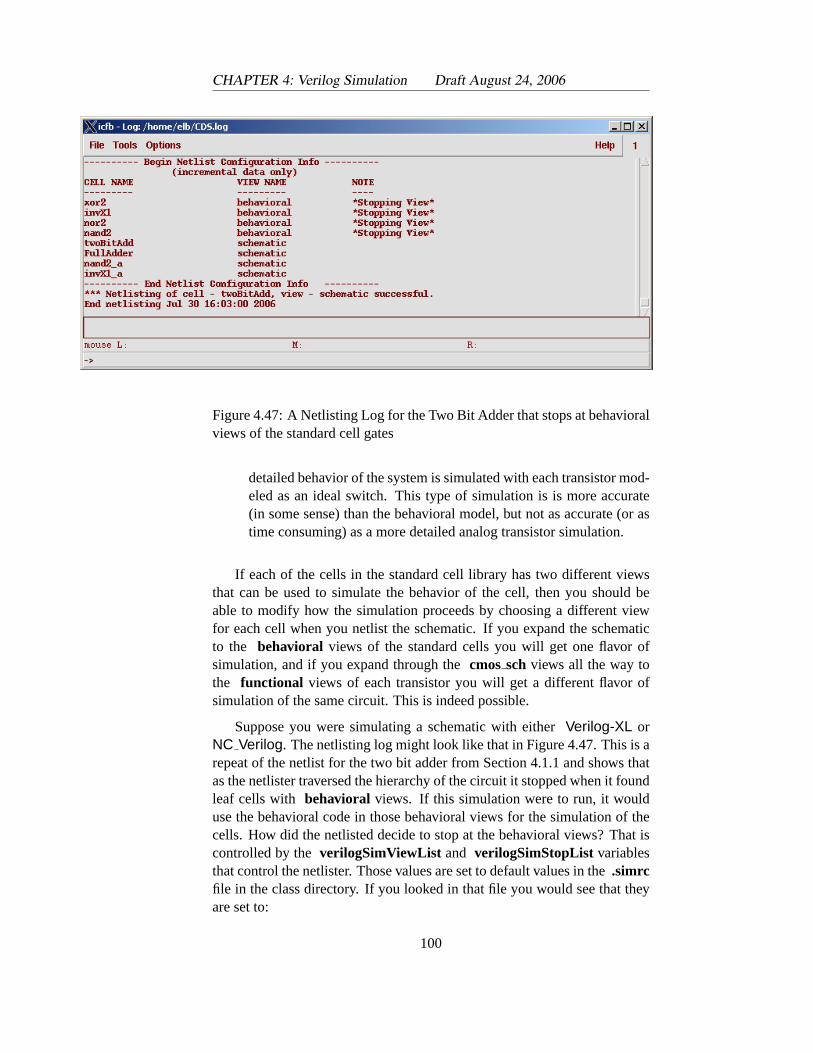
CHAPTER 4: Verilog Simulation Draft August 24, 2006
Figure 4.47: A Netlisting Log for the Two Bit Adder that stops at behavioralviews of the standard cell gates
detailed behavior of the system is simulated with each transistor mod-eled as an ideal switch. This type of simulation is is more accurate(in some sense) than the behavioral model, but not as accurate (or astime consuming) as a more detailed analog transistor simulation.
If each of the cells in the standard cell library has two different viewsthat can be used to simulate the behavior of the cell, then you should beable to modify how the simulation proceeds by choosing a different viewfor each cell when you netlist the schematic. If you expand the schematicto the behavioral views of the standard cells you will get one flavor ofsimulation, and if you expand through thecmossch views all the way tothe functional views of each transistor you will get a different flavor ofsimulation of the same circuit. This is indeed possible.
Suppose you were simulating a schematic with eitherVerilog-XL orNC Verilog. The netlisting log might look like that in Figure 4.47. This is arepeat of the netlist for the two bit adder from Section 4.1.1 and shows thatas the netlister traversed the hierarchy of the circuit it stopped when it foundleaf cells with behavioral views. If this simulation were to run, it woulduse the behavioral code in those behavioral views for the simulation of thecells. How did the netlisted decide to stop at the behavioral views? That iscontrolled by theverilogSimViewList and verilogSimStopList variablesthat control the netlister. Those values are set to default values in the.simrcfile in the class directory. If you looked in that file you would see that theyare set to:
100
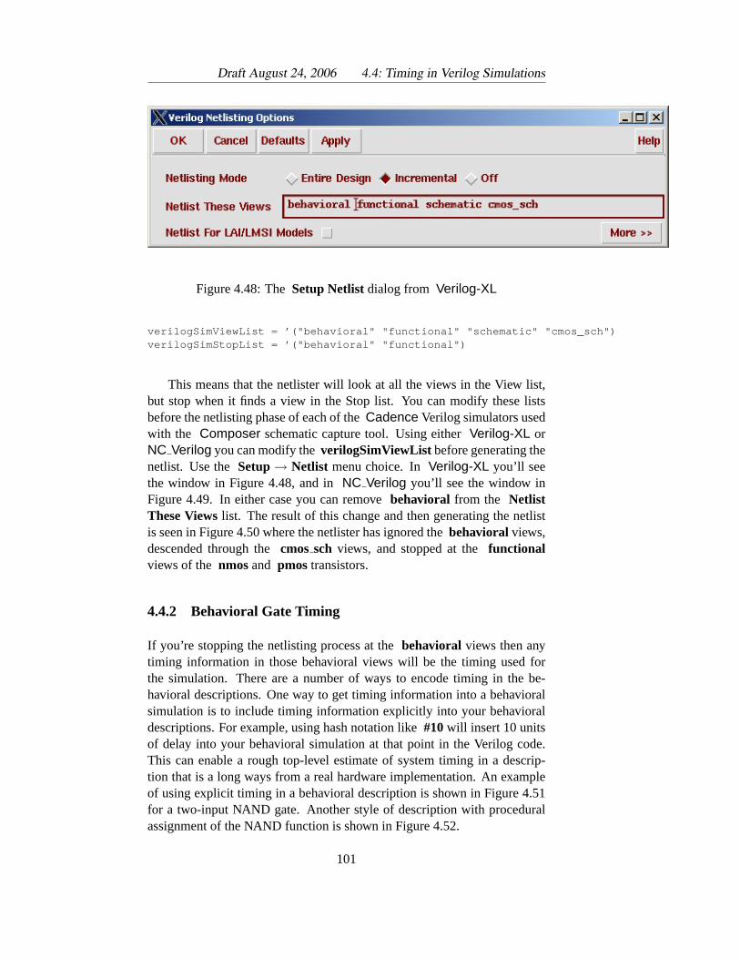
Draft August 24, 2006 4.4: Timing in Verilog Simulations
Figure 4.48: TheSetup Netlistdialog from Verilog-XL
verilogSimViewList = ’("behavioral" "functional" "schematic" "cmos_sch")verilogSimStopList = ’("behavioral" "functional")
This means that the netlister will look at all the views in the View list,but stop when it finds a view in the Stop list. You can modify these listsbefore the netlisting phase of each of theCadence Verilog simulators usedwith the Composer schematic capture tool. Using eitherVerilog-XL orNC Verilog you can modify theverilogSimViewList before generating thenetlist. Use theSetup→ Netlist menu choice. InVerilog-XL you’ll seethe window in Figure 4.48, and inNC Verilog you’ll see the window inFigure 4.49. In either case you can removebehavioral from the NetlistThese Viewslist. The result of this change and then generating the netlistis seen in Figure 4.50 where the netlister has ignored thebehavioral views,descended through thecmossch views, and stopped at thefunctionalviews of the nmosand pmostransistors.
4.4.2 Behavioral Gate Timing
If you’re stopping the netlisting process at thebehavioral views then anytiming information in those behavioral views will be the timing used forthe simulation. There are a number of ways to encode timing in the be-havioral descriptions. One way to get timing information into a behavioralsimulation is to include timing information explicitly into your behavioraldescriptions. For example, using hash notation like#10will insert 10 unitsof delay into your behavioral simulation at that point in the Verilog code.This can enable a rough top-level estimate of system timing in a descrip-tion that is a long ways from a real hardware implementation. An exampleof using explicit timing in a behavioral description is shown in Figure 4.51for a two-input NAND gate. Another style of description with proceduralassignment of the NAND function is shown in Figure 4.52.
101
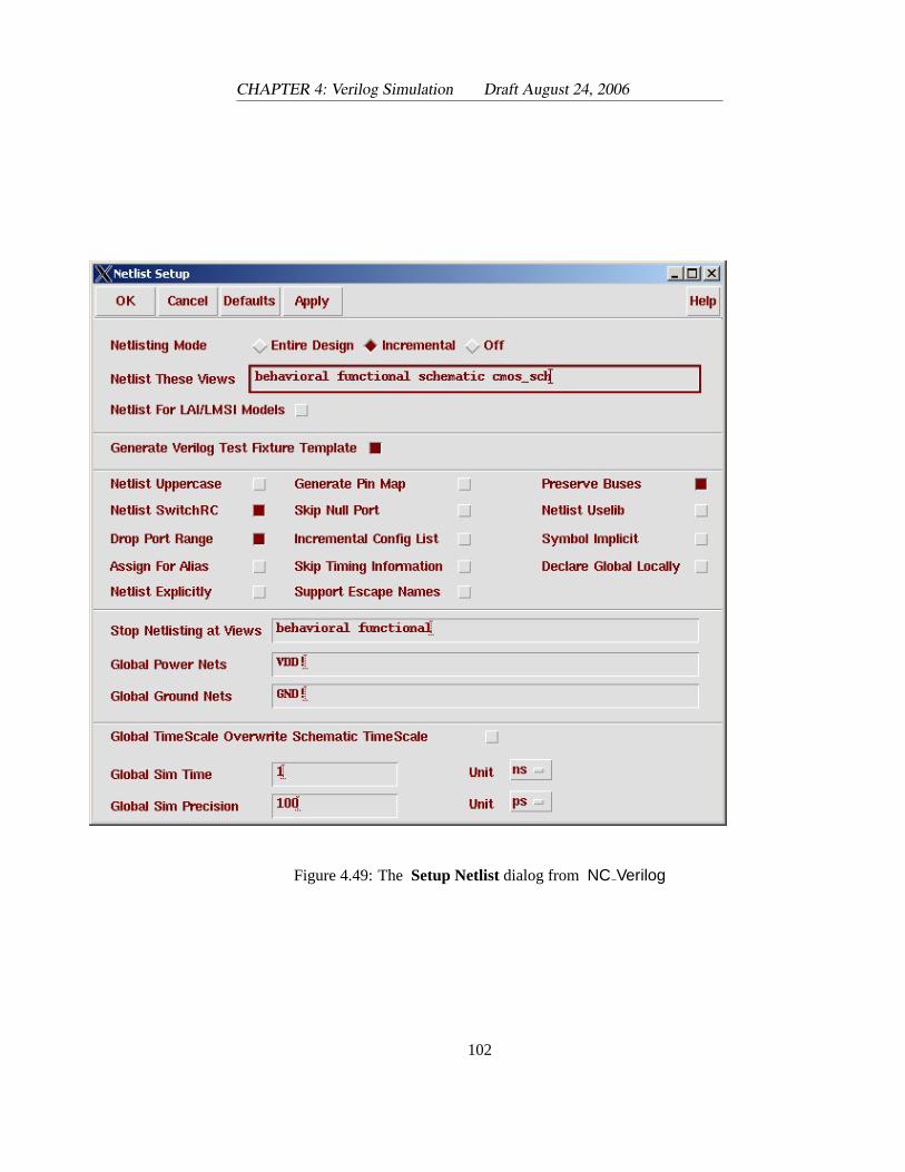
CHAPTER 4: Verilog Simulation Draft August 24, 2006
Figure 4.49: TheSetup Netlistdialog from NC Verilog
102
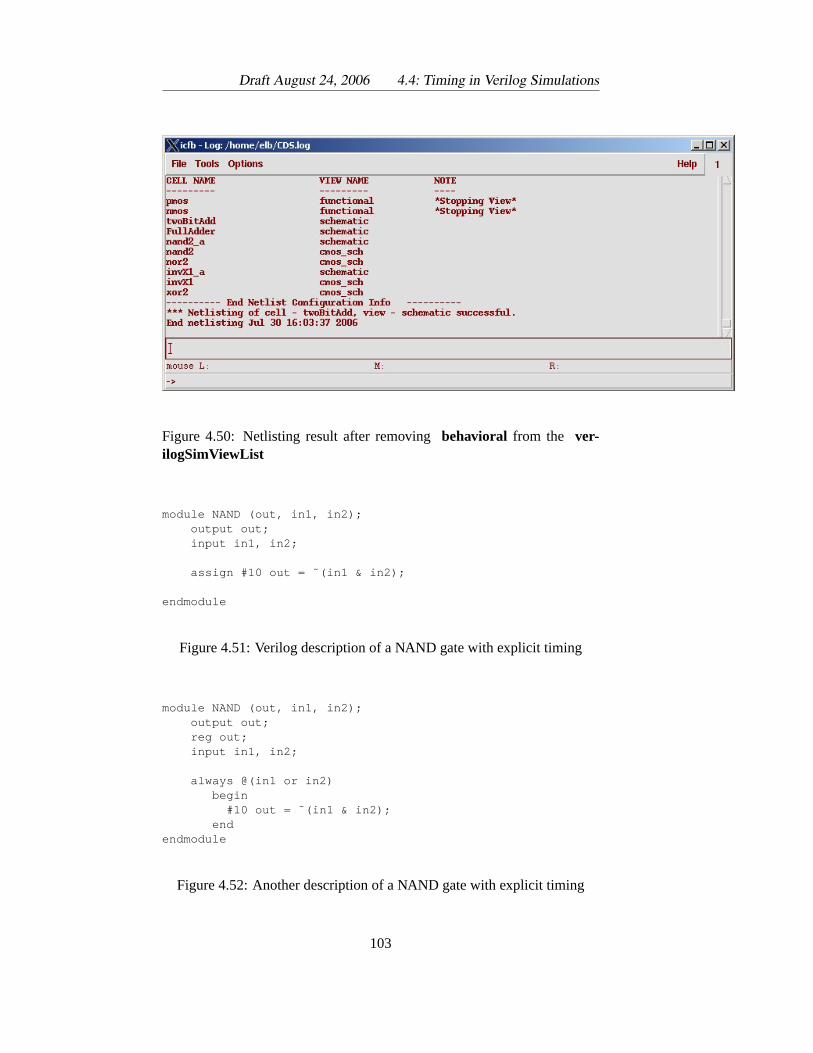
Draft August 24, 2006 4.4: Timing in Verilog Simulations
Figure 4.50: Netlisting result after removingbehavioral from the ver-ilogSimViewList
module NAND (out, in1, in2);output out;input in1, in2;
assign #10 out = ˜(in1 & in2);
endmodule
Figure 4.51: Verilog description of a NAND gate with explicit timing
module NAND (out, in1, in2);output out;reg out;input in1, in2;
always @(in1 or in2)begin
#10 out = ˜(in1 & in2);end
endmodule
Figure 4.52: Another description of a NAND gate with explicit timing
103
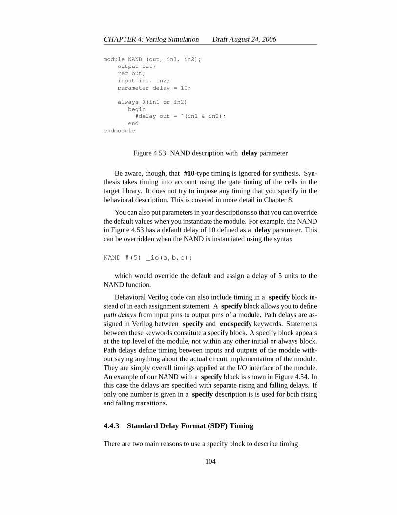
CHAPTER 4: Verilog Simulation Draft August 24, 2006
module NAND (out, in1, in2);output out;reg out;input in1, in2;parameter delay = 10;
always @(in1 or in2)begin
#delay out = ˜(in1 & in2);end
endmodule
Figure 4.53: NAND description withdelayparameter
Be aware, though, that#10-type timing is ignored for synthesis. Syn-thesis takes timing into account using the gate timing of the cells in thetarget library. It does not try to impose any timing that you specify in thebehavioral description. This is covered in more detail in Chapter 8.
You can also put parameters in your descriptions so that you can overridethe default values when you instantiate the module. For example, the NANDin Figure 4.53 has a default delay of 10 defined as adelay parameter. Thiscan be overridden when the NAND is instantiated using the syntax
NAND #(5) _io(a,b,c);
which would override the default and assign a delay of 5 units to theNAND function.
Behavioral Verilog code can also include timing in aspecifyblock in-stead of in each assignment statement. Aspecifyblock allows you to definepath delays from input pins to output pins of a module. Path delays are as-signed in Verilog betweenspecifyand endspecifykeywords. Statementsbetween these keywords constitute a specify block. A specify block appearsat the top level of the module, not within any other initial or always block.Path delays define timing between inputs and outputs of the module with-out saying anything about the actual circuit implementation of the module.They are simply overall timings applied at the I/O interface of the module.An example of our NAND with aspecifyblock is shown in Figure 4.54. Inthis case the delays are specified with separate rising and falling delays. Ifonly one number is given in aspecifydescription is is used for both risingand falling transitions.
4.4.3 Standard Delay Format (SDF) Timing
There are two main reasons to use a specify block to describe timing
104
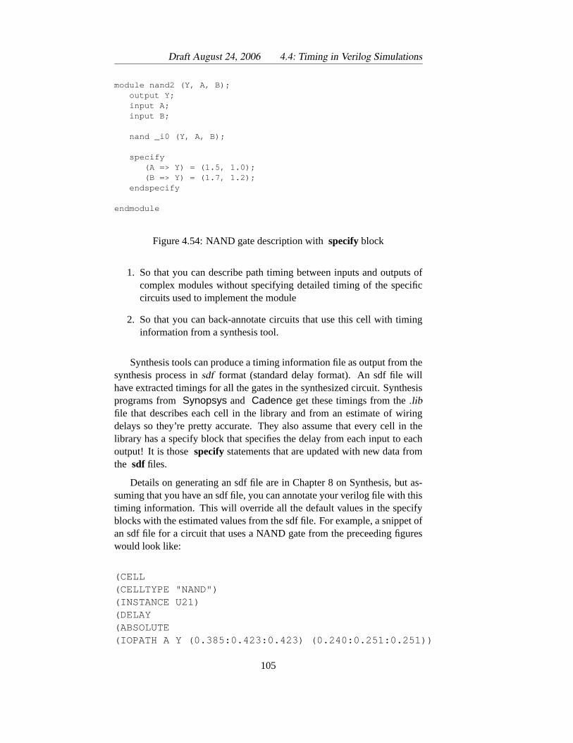
Draft August 24, 2006 4.4: Timing in Verilog Simulations
module nand2 (Y, A, B);output Y;input A;input B;
nand _i0 (Y, A, B);
specify(A => Y) = (1.5, 1.0);(B => Y) = (1.7, 1.2);
endspecify
endmodule
Figure 4.54: NAND gate description withspecifyblock
1. So that you can describe path timing between inputs and outputs ofcomplex modules without specifying detailed timing of the specificcircuits used to implement the module
2. So that you can back-annotate circuits that use this cell with timinginformation from a synthesis tool.
Synthesis tools can produce a timing information file as output from thesynthesis process insdf format (standard delay format). An sdf file willhave extracted timings for all the gates in the synthesized circuit. Synthesisprograms from Synopsys and Cadence get these timings from the.libfile that describes each cell in the library and from an estimate of wiringdelays so they’re pretty accurate. They also assume that every cell in thelibrary has a specify block that specifies the delay from each input to eachoutput! It is thosespecifystatements that are updated with new data fromthe sdf files.
Details on generating an sdf file are in Chapter 8 on Synthesis, but as-suming that you have an sdf file, you can annotate your verilog file with thistiming information. This will override all the default values in the specifyblocks with the estimated values from the sdf file. For example, a snippet ofan sdf file for a circuit that uses a NAND gate from the preceeding figureswould look like:
(CELL(CELLTYPE "NAND")(INSTANCE U21)(DELAY(ABSOLUTE(IOPATH A Y (0.385:0.423:0.423) (0.240:0.251:0.251))
105
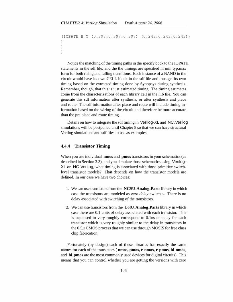
CHAPTER 4: Verilog Simulation Draft August 24, 2006
(IOPATH B Y (0.397:0.397:0.397) (0.243:0.243:0.243)))))
Notice the matching of the timing paths in the specify bock to the IOPATHstatements in the sdf file, and the the timings are specified in min:typ:maxform for both rising and falling transitions. Each instance of a NAND in thecircuit would have its own CELL block in the sdf file and thus get its owntiming based on the extracted timing done by Synopsys during synthesis.Remember, though, that this is just estimated timing. The timing estimatescome from the characterizations of each library cell in the .lib file. You cangenerate this sdf information after synthesis, or after synthesis and placeand route. The sdf information after place and route will include timing in-formation based on the wiring of the circuit and therefore be more accuratethan the pre place and route timing.
Details on how to integrate the sdf timing inVerilog-XL and NC Verilogsimulations will be postponed until Chapter 8 so that we can have structuralVerilog simulations and sdf files to use as examples.
4.4.4 Transistor Timing
When you use individualnmosand pmostransistors in your schematics (asdescribed in Section 3.3), and you simulate those schematics usingVerilog-XL or NC Verilog, what timing is associated with those primitive switch-level transistor models? That depends on how the transistor models aredefined. In our case we have two choices:
1. We can use transistors from theNCSU Analog Parts library in whichcase the transistors are modeled aszero delay switches. There is nodelay associated with switching of the transistors.
2. We can use transistors from theUofU Analog Parts library in whichcase there are 0.1 units of delay associated with each transistor. Thisis supposed to very roughly correspond to 0.1ns of delay for eachtransistor which is very roughly similar to the delay in transistors inthe 0.5µ CMOS process that we can use through MOSIS for free classchip fabrication.
Fortunately (by design) each of these libraries has exactly the samenames for each of the transistors (nmos, pmos, rnmos, r pmos, bi nmos,and bi pmosare the most commonly used devices for digital circuits). Thismeans that you can control whether you are getting the versions with zero
106
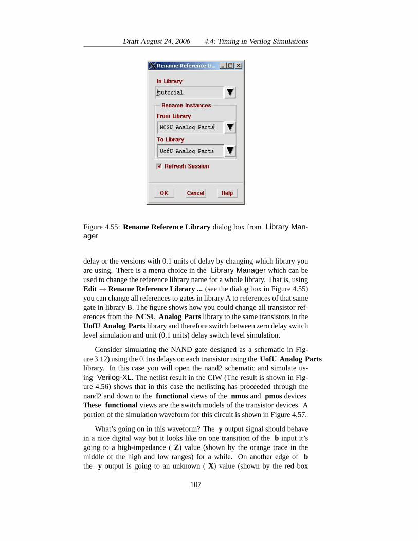
Draft August 24, 2006 4.4: Timing in Verilog Simulations
Figure 4.55:Rename Reference Librarydialog box from Library Man-ager
delay or the versions with 0.1 units of delay by changing which library youare using. There is a menu choice in theLibrary Manager which can beused to change the reference library name for a whole library. That is, usingEdit → Rename Reference Library ...(see the dialog box in Figure 4.55)you can change all references to gates in library A to references of that samegate in library B. The figure shows how you could change all transistor ref-erences from theNCSU Analog Parts library to the same transistors in theUofU Analog Parts library and therefore switch between zero delay switchlevel simulation and unit (0.1 units) delay switch level simulation.
Consider simulating the NAND gate designed as a schematic in Fig-ure 3.12) using the 0.1ns delays on each transistor using theUofU Analog Partslibrary. In this case you will open the nand2 schematic and simulate us-ing Verilog-XL. The netlist result in the CIW (The result is shown in Fig-ure 4.56) shows that in this case the netlisting has proceeded through thenand2 and down to thefunctional views of the nmosand pmosdevices.These functional views are the switch models of the transistor devices. Aportion of the simulation waveform for this circuit is shown in Figure 4.57.
What’s going on in this waveform? They output signal should behavein a nice digital way but it looks like on one transition of theb input it’sgoing to a high-impedance (Z) value (shown by the orange trace in themiddle of the high and low ranges) for a while. On another edge ofbthe y output is going to an unknown (X) value (shown by the red box
107
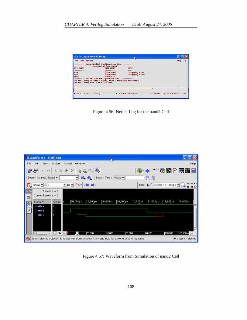
CHAPTER 4: Verilog Simulation Draft August 24, 2006
Figure 4.56: Netlist Log for the nand2 Cell
Figure 4.57: Waveform from Simulation of nand2 Cell
108
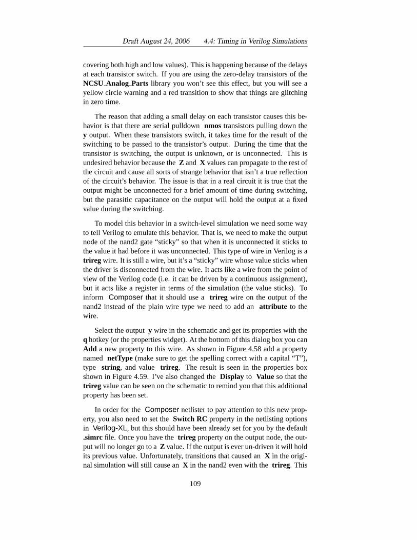
Draft August 24, 2006 4.4: Timing in Verilog Simulations
covering both high and low values). This is happening because of the delaysat each transistor switch. If you are using the zero-delay transistors of theNCSU Analog Parts library you won’t see this effect, but you will see ayellow circle warning and a red transition to show that things are glitchingin zero time.
The reason that adding a small delay on each transistor causes this be-havior is that there are serial pulldownnmos transistors pulling down they output. When these transistors switch, it takes time for the result of theswitching to be passed to the transistor’s output. During the time that thetransistor is switching, the output is unknown, or is unconnected. This isundesired behavior because theZ and X values can propagate to the rest ofthe circuit and cause all sorts of strange behavior that isn’t a true reflectionof the circuit’s behavior. The issue is that in a real circuit it is true that theoutput might be unconnected for a brief amount of time during switching,but the parasitic capacitance on the output will hold the output at a fixedvalue during the switching.
To model this behavior in a switch-level simulation we need some wayto tell Verilog to emulate this behavior. That is, we need to make the outputnode of the nand2 gate “sticky” so that when it is unconnected it sticks tothe value it had before it was unconnected. This type of wire in Verilog is atrireg wire. It is still a wire, but it’s a “sticky” wire whose value sticks whenthe driver is disconnected from the wire. It acts like a wire from the point ofview of the Verilog code (i.e. it can be driven by a continuous assignment),but it acts like a register in terms of the simulation (the value sticks). Toinform Composer that it should use atrireg wire on the output of thenand2 instead of the plain wire type we need to add anattribute to thewire.
Select the outputy wire in the schematic and get its properties with theq hotkey (or the properties widget). At the bottom of this dialog box you canAdd a new property to this wire. As shown in Figure 4.58 add a propertynamed netType (make sure to get the spelling correct with a capital “T”),type string, and value trireg . The result is seen in the properties boxshown in Figure 4.59. I’ve also changed theDisplay to Value so that thetrireg value can be seen on the schematic to remind you that this additionalproperty has been set.
In order for the Composer netlister to pay attention to this new prop-erty, you also need to set theSwitch RC property in the netlisting optionsin Verilog-XL, but this should have been already set for you by the default.simrc file. Once you have thetrireg property on the output node, the out-put will no longer go to aZ value. If the output is ever un-driven it will holdits previous value. Unfortunately, transitions that caused anX in the origi-nal simulation will still cause anX in the nand2 even with thetrireg . This
109
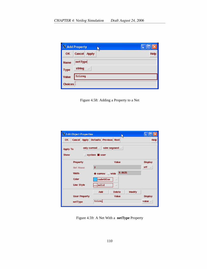
CHAPTER 4: Verilog Simulation Draft August 24, 2006
Figure 4.58: Adding a Property to a Net
Figure 4.59: A Net With anetTypeProperty
110
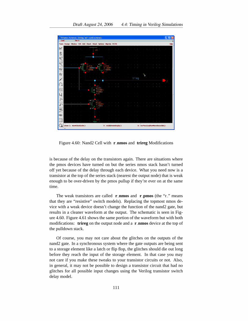
Draft August 24, 2006 4.4: Timing in Verilog Simulations
Figure 4.60: Nand2 Cell withr nmosand trireg Modifications
is because of the delay on the transistors again. There are situations wherethe pmos devices have turned on but the series nmos stack hasn’t turnedoff yet because of the delay through each device. What you need now is atransistor at the top of the series stack (nearest the output node) that is weakenough to be over-driven by the pmos pullup if they’re ever on at the sametime.
The weak transistors are calledr nmos and r pmos (the “r ” meansthat they are “resistive” switch models). Replacing the topmost nmos de-vice with a weak device doesn’t change the function of the nand2 gate, butresults in a cleaner waveform at the output. The schematic is seen in Fig-ure 4.60. Figure 4.61 shows the same portion of the waveform but with bothmodifications: trireg on the output node and ar nmosdevice at the top ofthe pulldown stack.
Of course, you may not care about the glitches on the outputs of thenand2 gate. In a synchronous system where the gate outputs are being sentto a storage element like a latch or flip flop, the glitches should die out longbefore they reach the input of the storage element. In that case you maynot care if you make these tweaks to your transistor circuits or not. Also,in general, it may not be possible to design a transistor circuit that had noglitches for all possible input changes using the Verilog transistor switchdelay model.
111
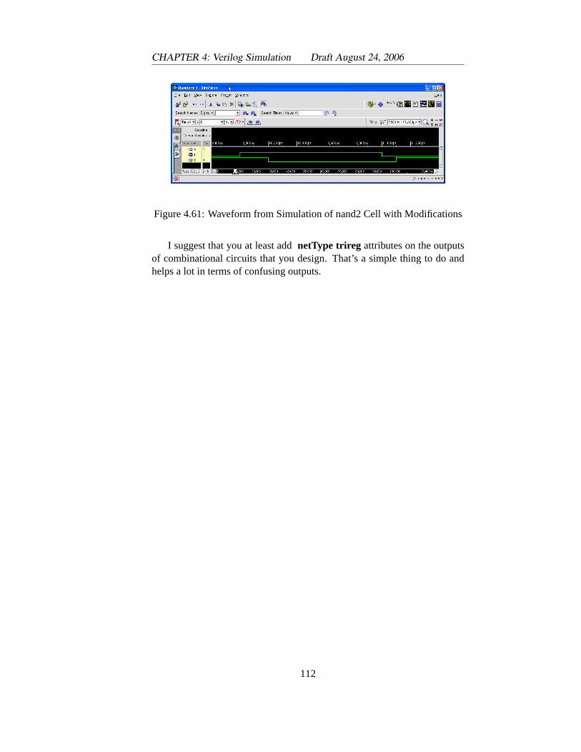
CHAPTER 4: Verilog Simulation Draft August 24, 2006
Figure 4.61: Waveform from Simulation of nand2 Cell with Modifications
I suggest that you at least addnetType trireg attributes on the outputsof combinational circuits that you design. That’s a simple thing to do andhelps a lot in terms of confusing outputs.
112
Chapter 5
Virtuoso Layout Editor
V IRTUOSO is the layout editor from Cadence that you use to drawthe composite layout for the fabrication of your circuit. It is partof the dfII tool suite. The process of drawing layout amounts to
drawing lots of colored rectangles with a graphical editor where each colorcorresponds to a fabrication layer on the integrated circuit. There are a lotof design rules for how those layers interact that must be followed verycarefully. The circuit decribed by these colored rectangles can be extractedfrom this graphic version and compared to the transistors in the schematic.The layout is eventually exported in standard format calledstreamor gdsIIand sent to the foundry to be fabricated.
This chapter will show how to to use theVirtuoso Layout Editor todraw the composite layout and how to check that the layout obeys designrules using DRC (Design Rule Checking). It’s also critical that the layoutcorrespond to the schematic that you wanted. A Layout Versus Schemtic(LVS) process will check that the extracted circuit from your layout matchesthe transistor schematic that you wanted. What we’re after is for all thedifferent views of a cell to match in terms of the information about the cellthat they share. Theschematicor cmosschview should describe the samecircuit that the layout view describes, thesymbol view should have thesame interface as both of those views, and thebehavioral view should alsoshare that interface. Eventually we’ll addextracted and abstract viewsfor other tools, which should also match the essential information. You mayalso useconfigviews for analog simulation.
5.1 An Inverter Schematic
We’ll demonstrate the layout process with a very simple inverter circuit.First you need aschematicview that describes the circuit you want. You
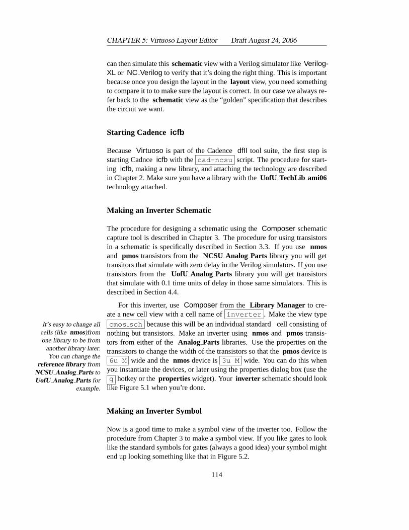
CHAPTER 5: Virtuoso Layout Editor Draft August 24, 2006
can then simulate thisschematicview with a Verilog simulator likeVerilog-XL or NC Verilog to verify that it’s doing the right thing. This is importantbecause once you design the layout in thelayout view, you need somethingto compare it to to make sure the layout is correct. In our case we always re-fer back to theschematicview as the “golden” specification that describesthe circuit we want.
Starting Cadence icfb
BecauseVirtuoso is part of the CadencedfII tool suite, the first step isstarting Cadnceicfb with the cad-ncsu script. The procedure for start-ing icfb, making a new library, and attaching the technology are describedin Chapter 2. Make sure you have a library with theUofU TechLib ami06technology attached.
Making an Inverter Schematic
The procedure for designing a schematic using theComposer schematiccapture tool is described in Chapter 3. The procedure for using transistorsin a schematic is specifically described in Section 3.3. If you usenmosand pmos transistors from theNCSU Analog Parts library you will gettransitors that simulate with zero delay in the Verilog simulators. If you usetransistors from theUofU Analog Parts library you will get transistorsthat simulate with 0.1 time units of delay in those same simulators. This isdescribed in Section 4.4.
For this inverter, useComposer from the Library Manager to cre-ate a new cell view with a cell name ofinverter . Make the view typecmos sch because this will be an individual standard cell consisting ofIt’s easy to change all
cells (like nmos)fromone library to be from
another library later.You can change the
reference library fromNCSU Analog Parts toUofU Analog Parts for
example.
nothing but transistors. Make an inverter usingnmos and pmos transis-tors from either of theAnalog Parts libraries. Use the properties on thetransistors to change the width of the transistors so that thepmosdevice is6u M wide and thenmosdevice is 3u M wide. You can do this when
you instantiate the devices, or later using the properties dialog box (use theq hotkey or theproperties widget). Your inverter schematic should look
like Figure 5.1 when you’re done.
Making an Inverter Symbol
Now is a good time to make a symbol view of the inverter too. Follow theprocedure from Chapter 3 to make a symbol view. If you like gates to looklike the standard symbols for gates (always a good idea) your symbol mightend up looking something like that in Figure 5.2.
114
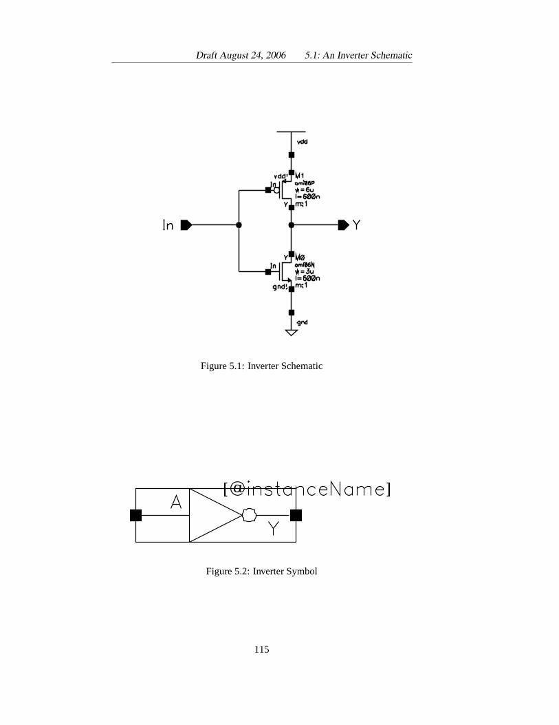
Draft August 24, 2006 5.1: An Inverter Schematic
Figure 5.1: Inverter Schematic
Figure 5.2: Inverter Symbol
115
CHAPTER 5: Virtuoso Layout Editor Draft August 24, 2006
Now check and savethe symbol and cmosschviews. They shouldboth check and save without errors before you proceed to the layout!
5.2 Layout for an Inverter
The process of drawing CMOS layout is to use the graphical editor toNote that there is atutorial on Virtuoso
that comes with thetools. Although it will
not use our sametechnology information
it may show you evenmore tricks of the tools.
draw colored rectangles that represent the fabrication layers in the CMOSfabrication process.
Creating a new layout view
In the Library Manger , in the same library as you used for theinvertercmosschview, create a new cell view. This cell view should have theCellName of inverter so that it will be a different view of the same in-verter cell. The view type should belayout , and the tool should be
Virtuoso (see Figure 5.3).
This will open up two windows; TheVirtuoso Editing window wherethe layout is drawn and theLSW (Layer Select Window), where you selectthe layers (diffusion, metal1, metal2, polysilicon, etc) to draw.
If the layout is going to be a Standard Cell, the height of the cell as wellas the width of the VDD and VSS power supply wires must be defined sothat cells can eventually abut each other and have the power supply connec-tions made automatically as the cells abut each other. To avoid DRC errorswhen abutting the cells, it is also important to keep the left and right bor-ders of the cell free of any drawing that might cause an error when the cellis abutted to another cell. The n-tub is usually aligned with the cell bor-ders so that it connects into a seamless rectangle when abutted. Usually celltemplates of standard heights containing VDD and VSS contacts (wires) aswell as default nwell dimensions are used. For this tutorial, you can justpick some reasonable dimensions, but keep in mind that later you’ll want toplan for a particular power pitch.
Drawing an nmos transistor
Click on the nactive (light green) layer in the LSW window. In the Vir-There are two types ofactive defined in our
technlogy file: nactiveand pactive. They’re
different colors so youcan tell them apart.
tuoso Layout Editor window, pressr to activate the Rectangle command.Now you can draw a rectangle by selecting the start and end points of therectangle. This firstnactive rectangle is shown in Figure 5.4.
Press k to activate the Ruler command. You can click on one ofthe corners of the green rectangle to place the ruler and measure the sides
116
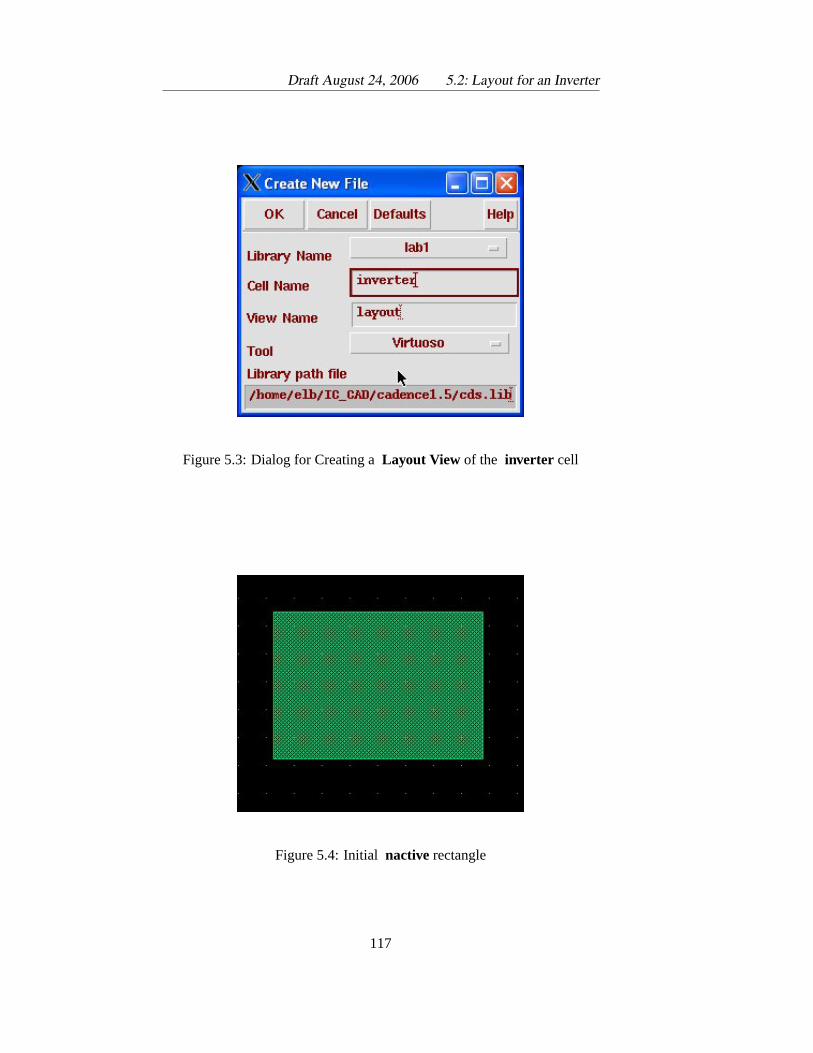
Draft August 24, 2006 5.2: Layout for an Inverter
Figure 5.3: Dialog for Creating aLayout View of the inverter cell
Figure 5.4: Initial nactive rectangle
117
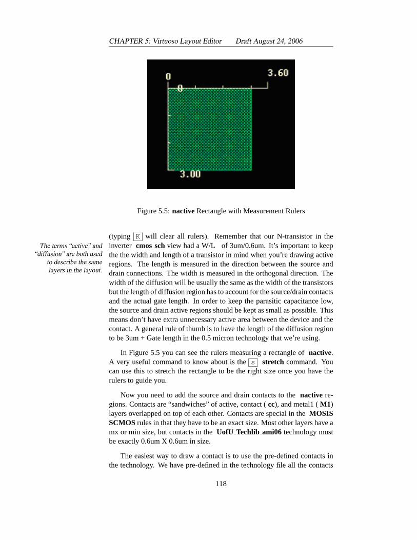
CHAPTER 5: Virtuoso Layout Editor Draft August 24, 2006
Figure 5.5:nactiveRectangle with Measurement Rulers
(typing K will clear all rulers). Remember that our N-transistor in theinverter cmosschview had a W/L of 3um/0.6um. It’s important to keepThe terms “active” and
“diffusion” are both usedto describe the samelayers in the layout.
the the width and length of a transistor in mind when you’re drawing activeregions. The length is measured in the direction between the source anddrain connections. The width is measured in the orthogonal direction. Thewidth of the diffusion will be usually the same as the width of the transistorsbut the length of diffusion region has to account for the source/drain contactsand the actual gate length. In order to keep the parasitic capacitance low,the source and drain active regions should be kept as small as possible. Thismeans don’t have extra unnecessary active area between the device and thecontact. A general rule of thumb is to have the length of the diffusion regionto be 3um + Gate length in the 0.5 micron technology that we’re using.
In Figure 5.5 you can see the rulers measuring a rectangle ofnactive.A very useful command to know about is thes stretch command. Youcan use this to stretch the rectangle to be the right size once you have therulers to guide you.
Now you need to add the source and drain contacts to thenactive re-gions. Contacts are “sandwiches” of active, contact (cc), and metal1 (M1)layers overlapped on top of each other. Contacts are special in theMOSISSCMOS rules in that they have to be an exact size. Most other layers have amx or min size, but contacts in theUofU Techlib ami06 technology mustbe exactly 0.6um X 0.6um in size.
The easiest way to draw a contact is to use the pre-defined contacts inthe technology. We have pre-defined in the technology file all the contacts
118
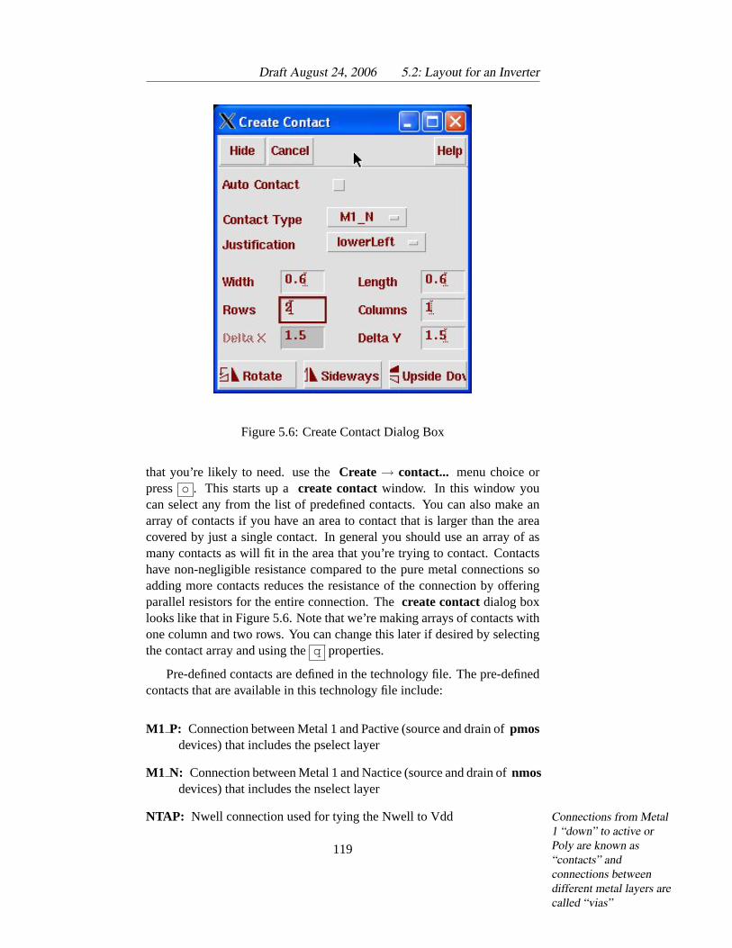
Draft August 24, 2006 5.2: Layout for an Inverter
Figure 5.6: Create Contact Dialog Box
that you’re likely to need. use theCreate→ contact... menu choice orpress o . This starts up acreate contactwindow. In this window youcan select any from the list of predefined contacts. You can also make anarray of contacts if you have an area to contact that is larger than the areacovered by just a single contact. In general you should use an array of asmany contacts as will fit in the area that you’re trying to contact. Contactshave non-negligible resistance compared to the pure metal connections soadding more contacts reduces the resistance of the connection by offeringparallel resistors for the entire connection. Thecreate contactdialog boxlooks like that in Figure 5.6. Note that we’re making arrays of contacts withone column and two rows. You can change this later if desired by selectingthe contact array and using theq properties.
Pre-defined contacts are defined in the technology file. The pre-definedcontacts that are available in this technology file include:
M1 P: Connection between Metal 1 and Pactive (source and drain ofpmosdevices) that includes the pselect layer
M1 N: Connection between Metal 1 and Nactice (source and drain ofnmosdevices) that includes the nselect layer
NTAP: Nwell connection used for tying the Nwell to Vdd Connections from Metal1 “down” to active orPoly are known as“contacts” andconnections betweendifferent metal layers arecalled “vias”
119
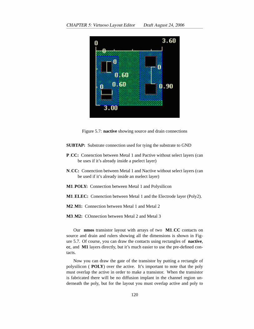
CHAPTER 5: Virtuoso Layout Editor Draft August 24, 2006
Figure 5.7:nactiveshowing source and drain connections
SUBTAP: Substrate connection used for tying the substrate to GND
P CC: Conenction between Metal 1 and Pactive without select layers (canbe uses if it’s already inside a pselect layer)
N CC: Conenction between Metal 1 and Nactive without select layers (canbe used if it’s already inside an nselect layer)
M1 POLY: Connection between Metal 1 and Polysilicon
M1 ELEC: Conenction between Metal 1 and the Electrode layer (Poly2).
M2 M1: Connection between Metal 1 and Metal 2
M3 M2: COnnection between Metal 2 and Metal 3
Our nmos transistor layout with arrays of twoM1 CC contacts onsource and drain and rulers showing all the dimensions is shown in Fig-ure 5.7. Of course, you can draw the contacts using rectangles ofnactive,cc, and M1 layers directly, but it’s much easier to use the pre-defined con-tacts.
Now you can draw the gate of the transistor by putting a rectangle ofpolysilicon ( POLY ) over the active. It’s important to note that the polymust overlap the active in order to make a transistor. When the transistoris fabricated there will be no diffusion implant in the channel region un-derneath the poly, but for the layout you must overlap active and poly to
120
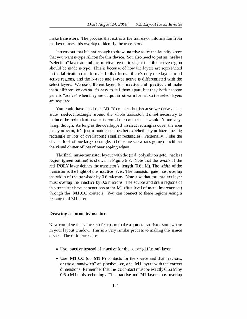
Draft August 24, 2006 5.2: Layout for an Inverter
make transistors. The process that extracts the transistor information fromthe layout uses this overlap to identify the transistors.
It turns out that it’s not enough to drawnactive to let the foundty knowthat you want n-type silicon for this device. You also need to put annselect“selection” layer around thenactive region to signal that this active regionshould be made n-type. This is because of how the layers are represnetedin the fabrication data format. In that format there’s only one layer for allactive regions, and the N-type and P-type active is differentiated with theselect layers. We use different layers fornactive and pactive and makethem different colors so it’s easy to tell them apart, but they both becomegeneric “active” when they are output instream format so the select layersare required.
You could have used theM1 N contacts but because we drew a sep-arate nselectrectangle around the whole transistor, it’s not necessary toinclude the redundantnselectaround the contacts. It wouldn’t hurt any-thing, though. As long as the overlappednselectrectangles cover the areathat you want, it’s just a matter of anesthetics whether you have one bigrectangle or lots of overlapping smaller rectangles. Personally, I like thecleaner look of one large rectangle. It helps me see what’s going on withoutthe visual clutter of lots of overlapping edges.
The final nmostransistor layout with the (red) polysilicon gate,nselectregion (green outline) is shown in Figure 5.8. Note that thewidth of thered POLY layer defines the transistor’slength (0.6u M). Thewidth of thetransistor is the hight of thenactive layer. The transistor gate must overlapthe width of the transistor by 0.6 microns. Note also that thenselectlayermust overlap thenactive by 0.6 microns. The source and drain regions ofthis transistor have conenctions to the M1 (first level of metal interconnect)through the M1 CC contacts. You can connect to these regions using arectangle of M1 later.
Drawing a pmos transistor
Now complete the same set of steps to make apmos transistor somewherein your layout window. This is a very similar process to making thenmosdevice. The differences are:
• Use pactive instead ofnactive for the active (diffusion) layer.
• Use M1 CC (or M1 P) contacts for the source and drain regions,or use a “sandwich” ofpactive, cc, and M1 layers with the correctdimensions. Remember that thecccontact must be exactly 0.6u M by0.6 u M in this technology. Thepactiveand M1 layers must overlap
121
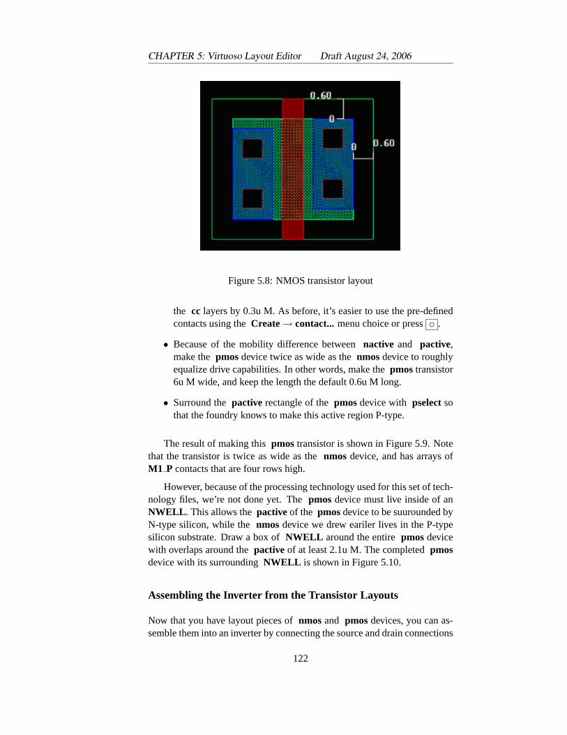
CHAPTER 5: Virtuoso Layout Editor Draft August 24, 2006
Figure 5.8: NMOS transistor layout
the cc layers by 0.3u M. As before, it’s easier to use the pre-definedcontacts using theCreate→ contact...menu choice or presso .
• Because of the mobility difference betweennactive and pactive,make thepmosdevice twice as wide as thenmosdevice to roughlyequalize drive capabilities. In other words, make thepmostransistor6u M wide, and keep the length the default 0.6u M long.
• Surround thepactive rectangle of thepmosdevice with pselectsothat the foundry knows to make this active region P-type.
The result of making thispmos transistor is shown in Figure 5.9. Notethat the transistor is twice as wide as thenmos device, and has arrays ofM1 P contacts that are four rows high.
However, because of the processing technology used for this set of tech-nology files, we’re not done yet. Thepmos device must live inside of anNWELL . This allows thepactiveof the pmosdevice to be suurounded byN-type silicon, while thenmosdevice we drew eariler lives in the P-typesilicon substrate. Draw a box ofNWELL around the entirepmosdevicewith overlaps around thepactive of at least 2.1u M. The completedpmosdevice with its surroundingNWELL is shown in Figure 5.10.
Assembling the Inverter from the Transistor Layouts
Now that you have layout pieces ofnmosand pmosdevices, you can as-semble them into an inverter by connecting the source and drain connections
122
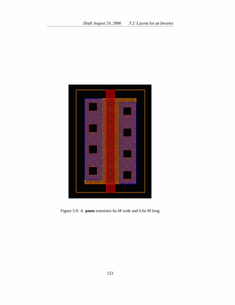
Draft August 24, 2006 5.2: Layout for an Inverter
Figure 5.9: A pmostransistor 6u M wide and 0.6u M long
123
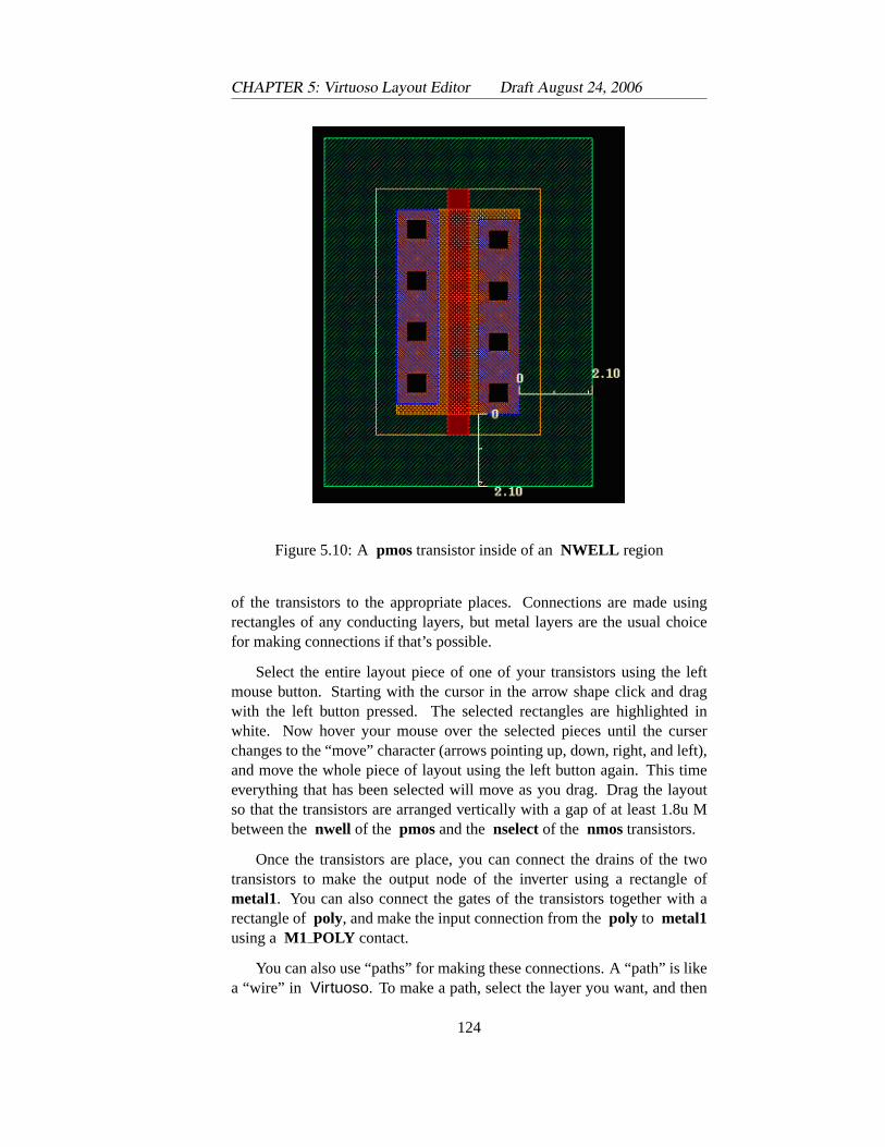
CHAPTER 5: Virtuoso Layout Editor Draft August 24, 2006
Figure 5.10: Apmostransistor inside of anNWELL region
of the transistors to the appropriate places. Connections are made usingrectangles of any conducting layers, but metal layers are the usual choicefor making connections if that’s possible.
Select the entire layout piece of one of your transistors using the leftmouse button. Starting with the cursor in the arrow shape click and dragwith the left button pressed. The selected rectangles are highlighted inwhite. Now hover your mouse over the selected pieces until the curserchanges to the “move” character (arrows pointing up, down, right, and left),and move the whole piece of layout using the left button again. This timeeverything that has been selected will move as you drag. Drag the layoutso that the transistors are arranged vertically with a gap of at least 1.8u Mbetween thenwell of the pmosand thenselectof the nmostransistors.
Once the transistors are place, you can connect the drains of the twotransistors to make the output node of the inverter using a rectangle ofmetal1. You can also connect the gates of the transistors together with arectangle ofpoly, and make the input connection from thepoly to metal1using a M1 POLY contact.
You can also use “paths” for making these connections. A “path” is likea “wire” in Virtuoso. To make a path, select the layer you want, and then
124
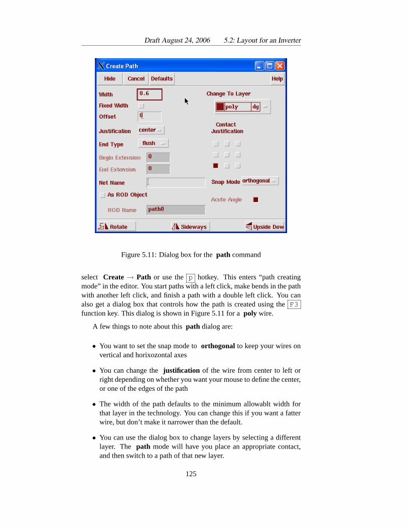
Draft August 24, 2006 5.2: Layout for an Inverter
Figure 5.11: Dialog box for thepath command
select Create → Path or use the p hotkey. This enters “path creatingmode” in the editor. You start paths with a left click, make bends in the pathwith another left click, and finish a path with a double left click. You canalso get a dialog box that controls how the path is created using theF3function key. This dialog is shown in Figure 5.11 for apoly wire.
A few things to note about thispath dialog are:
• You want to set the snap mode toorthogonal to keep your wires onvertical and horixozontal axes
• You can change thejustification of the wire from center to left orright depending on whether you want your mouse to define the center,or one of the edges of the path
• The width of the path defaults to the minimum allowablt width forthat layer in the technology. You can change this if you want a fatterwire, but don’t make it narrower than the default.
• You can use the dialog box to change layers by selecting a differentlayer. The path mode will have you place an appropriate contact,and then switch to a path of that new layer.
125
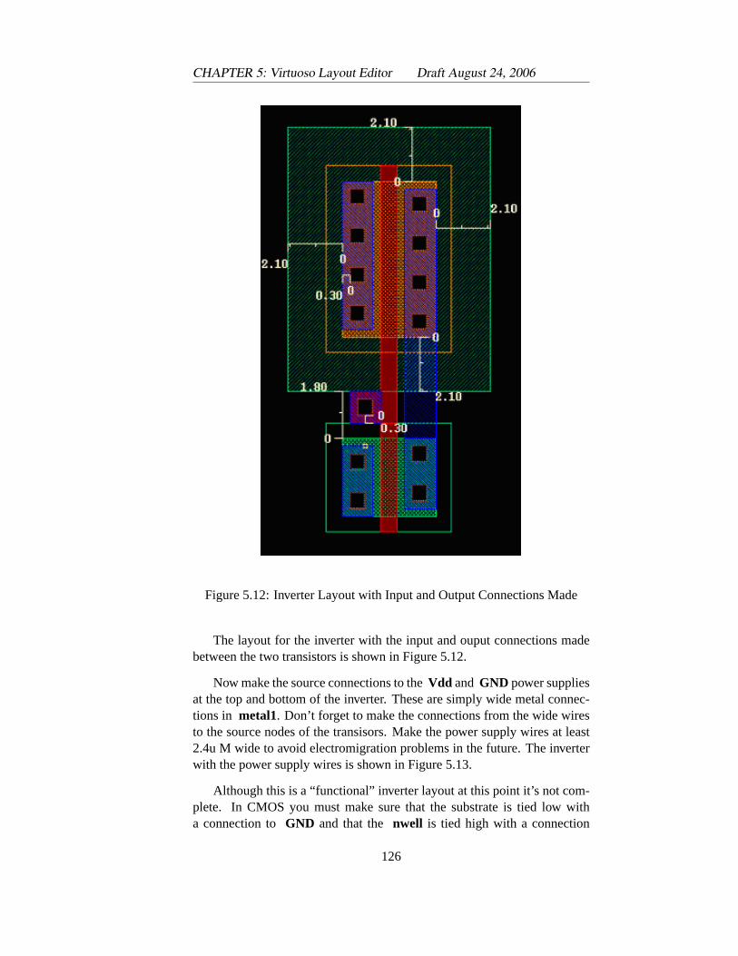
CHAPTER 5: Virtuoso Layout Editor Draft August 24, 2006
Figure 5.12: Inverter Layout with Input and Output Connections Made
The layout for the inverter with the input and ouput connections madebetween the two transistors is shown in Figure 5.12.
Now make the source connections to theVdd and GND power suppliesat the top and bottom of the inverter. These are simply wide metal connec-tions in metal1. Don’t forget to make the connections from the wide wiresto the source nodes of the transisors. Make the power supply wires at least2.4u M wide to avoid electromigration problems in the future. The inverterwith the power supply wires is shown in Figure 5.13.
Although this is a “functional” inverter layout at this point it’s not com-plete. In CMOS you must make sure that the substrate is tied low witha connection toGND and that the nwell is tied high with a connection
126
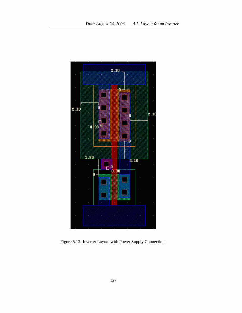
Draft August 24, 2006 5.2: Layout for an Inverter
Figure 5.13: Inverter Layout with Power Supply Connections
127

CHAPTER 5: Virtuoso Layout Editor Draft August 24, 2006
to Vdd to avoid latchup effects due to the parasitic devices formed by thewells. These contacts are most easily made using theSUBTAP and NTAPpre-defined contacts int he technology. These taps are contacts from thenactive and pactive active regions tometal1, but they are meant specifi-cally for connections to the well and substrate. Any connection topactivewhich is outside of annwell is a substrate connection, and any connectionto nactive inside of an nwell is a well connection. These contacts area standard width so that they can be tiled in a consistant way. When youstart fitting your cells to the library template you will see that cells in theUofU Digital library are sized in units of 2.4u M chunks that match withthe well and substrate tap widths for convenience.
The inverter with the well and substrate connections is shown in Fig-ure 5.14. Thenwell layer in this example has been extended by 0.3u Mbeyond theVdd metal layer to make it easier to abut these cells in a largerlayout later on.
Finally, we need to add connection name information to our layout. Re-member that all the different views of a cell must be consistant in their I/Ointerface (at least). The invertercmossch view and symbol view eachRemember that Verilog
names are case sensitive have an input connection namedIn and an output connection namedOut.In addition, our layout needs to identify the power supply connections ex-plicitly. We’ll specify the power supply connections with the namesvdd!and gnd!. The “!” character is a flag to make these names global. If youdon’t use this flag you will have to export your power supply connections aspins to your cell. That’s not incorrect, it’s just a hassle.
In order to make connections in the layout view we need to addpins tothe design. Pins are similar to the red-arrow pins in thecmosschview,but in the layout we identify pieces of the layout with the pins. These arecalled shape pinsbecause they identify a shape in the layout with the pin.There are other types of pins you can make inVirtuoso but please use onlyshape pinsin this tool flow because other steps in the process depend onthis.
A shape pinis a piece of layout (a rectangle) in a particular layer (i.e.metal1) that also has a pin name attached to it. Add ashape pinusing theCreate→ Pin menu choice. The dialog box is shown in Figure 5.15. Notethat you won’t see this exact dialog box until you selectshape pinas the pintype. Once you are in theshape pindialog box, make sure that you haveselected theDisplay Pin Nameoption, that you’re placing a rectangle, thatyou have selected the correct direction for the pin (i.e.input ), and that youhave entered the name (or names) you want to add. You select the layer thatyou want the pin to be made in (i.e.metal1) in the LSW (Layer SelectionWindow). When all this is correct, draw a rectangle of the layer in the spotthat you want to have identified with the connection pin in the layout.
128
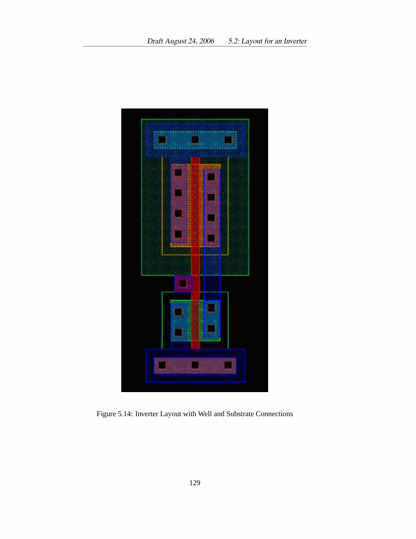
Draft August 24, 2006 5.2: Layout for an Inverter
Figure 5.14: Inverter Layout with Well and Substrate Connections
129
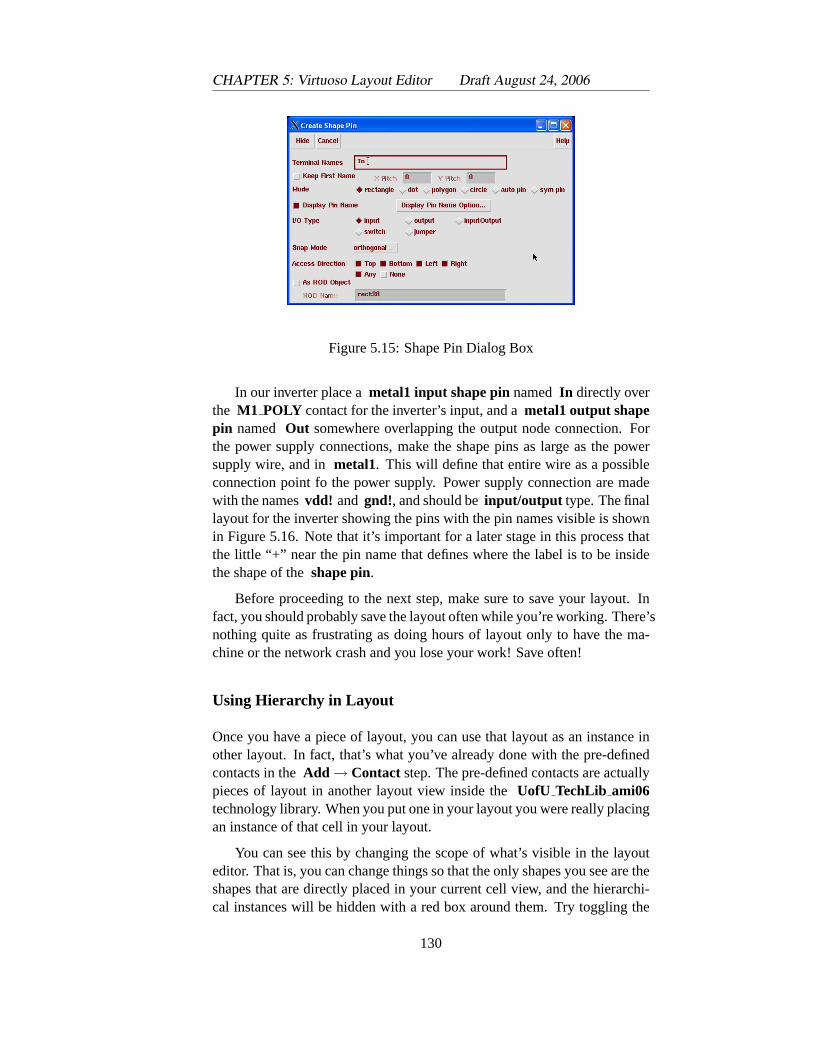
CHAPTER 5: Virtuoso Layout Editor Draft August 24, 2006
Figure 5.15: Shape Pin Dialog Box
In our inverter place ametal1 input shape pinnamed In directly overthe M1 POLY contact for the inverter’s input, and ametal1 output shapepin named Out somewhere overlapping the output node connection. Forthe power supply connections, make the shape pins as large as the powersupply wire, and inmetal1. This will define that entire wire as a possibleconnection point fo the power supply. Power supply connection are madewith the namesvdd! and gnd!, and should beinput/output type. The finallayout for the inverter showing the pins with the pin names visible is shownin Figure 5.16. Note that it’s important for a later stage in this process thatthe little “+” near the pin name that defines where the label is to be insidethe shape of theshape pin.
Before proceeding to the next step, make sure to save your layout. Infact, you should probably save the layout often while you’re working. There’snothing quite as frustrating as doing hours of layout only to have the ma-chine or the network crash and you lose your work! Save often!
Using Hierarchy in Layout
Once you have a piece of layout, you can use that layout as an instance inother layout. In fact, that’s what you’ve already done with the pre-definedcontacts in theAdd → Contact step. The pre-defined contacts are actuallypieces of layout in another layout view inside theUofU TechLib ami06technology library. When you put one in your layout you were really placingan instance of that cell in your layout.
You can see this by changing the scope of what’s visible in the layouteditor. That is, you can change things so that the only shapes you see are theshapes that are directly placed in your current cell view, and the hierarchi-cal instances will be hidden with a red box around them. Try toggling the
130
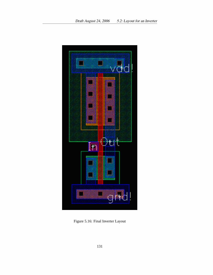
Draft August 24, 2006 5.2: Layout for an Inverter
Figure 5.16: Final Inverter Layout
131
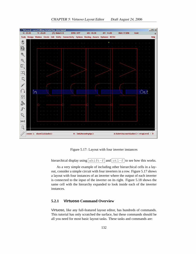
CHAPTER 5: Virtuoso Layout Editor Draft August 24, 2006
Figure 5.17: Layout with four inverter instances
hierarchical display usingshift-f and ctl-f to see how this works.
As a very simple example of including other hierarchical cells in a lay-out, consider a simple circuit with four inverters in a row. Figure 5.17 showsa layout with four instances of an inverter where the output of each inverteris connected to the input of the inverter on its right. Figure 5.18 shows thesame cell with the hierarchy expanded to look inside each of the inverterinstances.
5.2.1 Virtuoso Command Overview
Virtuoso, like any full-featured layout editor, has hundreds of commands.This tutorial has only scratched the surface, but these commands should beall you need for most basic layout tasks. These tasks and commands are:
132
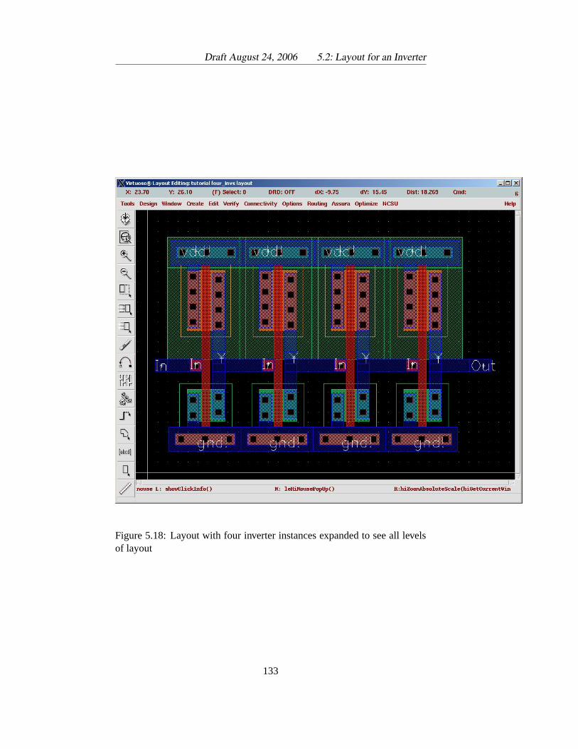
Draft August 24, 2006 5.2: Layout for an Inverter
Figure 5.18: Layout with four inverter instances expanded to see all levelsof layout
133
CHAPTER 5: Virtuoso Layout Editor Draft August 24, 2006
Drawing Rectangles: The basic components of alayout view are coloredrectangles that represent fabrication layers. Layers are selected inthe LSW Layer Selection Window. Rectangles are drawn with theCreate→ Rectanglemenu choice, the rectangle widget, or therhotkey.
Connecting Rectangles:Rectangles of the same material are electricallyconnected by abutment or by overlapping. Rectangles of differentmaterials are electrically connected using contacts or vias. These canbe drawn with a “sandwich” of layers with an appropriate contactshape between them (cc) for connecting metal1 “down” to activeor poly, and via<n> for connecting metal<n> to metal<n+1>.So, for connectingmetal2 to metal3 a via2 is used. Vias and con-tacts must be exactly 0.6u M by 0.6u M in thisUofU Techlib ami06technology.
Using Paths: A convenient way to draw “wires” out of rectangles is to usethe path feature through theCreate→ Path... menu choice or thep hotkey. Choose the layer from theLSW. Single-click the left
button to change directions, double click the left button to end a wire.
Moving and Stretching: Select layout using the left button, or click anddrag to select groups of layout objects. If the cursor changes to the“movement arrows” you can move the selected shapes using the leftbutton with click and drag. Reshapping can be done with theStretch(hotkey s ) command.
Changing the View Hierarchy: You can choose how many levels of hier-archy to view using theOptions→ Display meny choice and changethe Display Levelsnumbers. You can also use thectl-f hotkeyto hide all but the top level, andF (shift-f) hotkey to expand the dis-play to all levels of the hierarchy. Note that thef hotkey fills andcenters on the screen with the current cell.
Viewing Connectivity: You can use theConnectivity→Mark Net menyto mark an entire connected net. This will highlight the entire con-nected net through all conducting layers. Note that it does notselectthat net, it simply marks it so you can see what’s connected to what.
Hierarchical Instantiation: You can include instances of other layout cellsin your current layout with theCreate→ Instance menu, the ihotkey, or the instance widget. These instances will show up asblank boxes with a red outline if you are not viewing deep enoughin the hierarchy, and as filled in layouts if you have expanded theviewing hierarchy.
134
Draft August 24, 2006 5.3: Printing Layouts
5.3 Printing Layouts
In order to print your layout view you can use theDesign→ Plot → Sub-mit... menu. This will submit your design to be plotted (printed) either ona printer or to a file. TheSubmit Plot dialog box is shown in Figure 5.19.This Figure shows the dialog box after the plotter has been configured tosend the output to an EPS (Encapsulated PostScript) file on A-sized paperto a file calledfoo.ps. These choices are set up in thePlot Options... dialogbox as seen in Figure 5.20. In this dialog you can select the plotter (printer)that you would like to send the graphics to. You can either select a printername (like the CADE printer), or save the file as EPS. You can choose tocenter the plot, fit it to the page, or scale the plot to whatever size you like.You can also choose to queue the plot for a later time, change the name ofthe file (if you’re plotting to a file), and choose to have email sent when theplotting completes (a somewhat silly feature, unless you’re really queuingthe plot for sometime later). The EPS option will print to a color postscriptfile so that if you have access to a color printer you can print in color. I liketo un-select thePlot With Header option so that I don’t get an extra headerpage included with the plot.
5.4 Design Rule Checking
Because there are so many rules about how you can draw shapes in thedifferent mask layers, it’s very hard to tell just by looking if you have obeyedall the design rules (The MOSIS SCMOS rev8 design rules are shown inAppendix D). Letting the CAD tool check the design rules for you is knownasDesign Rule Checking or DRC. When you’re drawing new layout usingVirtuoso it’s helpful to run the DRC check frequently as you’re doing yourlayout. There are three DRC tools that we have access to in this CAD flow,but only DIVA is currently fully supported for our class technology. Thetools are:
DIVA: This is the DRC engine that is integrated withVirtuoso and sup-ported by our current class technology files. It will be described indetail in the next section.
Assura : This is a faster and more capable DRC engine that is also inte-grated with Virtuoso, but not yet fully supported by our technologyinformation. It uses a different DRC rules file that is currently underdevelopment.
Calibre : This is the “industry standard” DRC engine fromMentor. Itrequires yet a different DRC rules file so it’s not supported by our
135
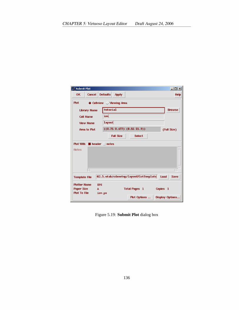
CHAPTER 5: Virtuoso Layout Editor Draft August 24, 2006
Figure 5.19:Submit Plot dialog box
136
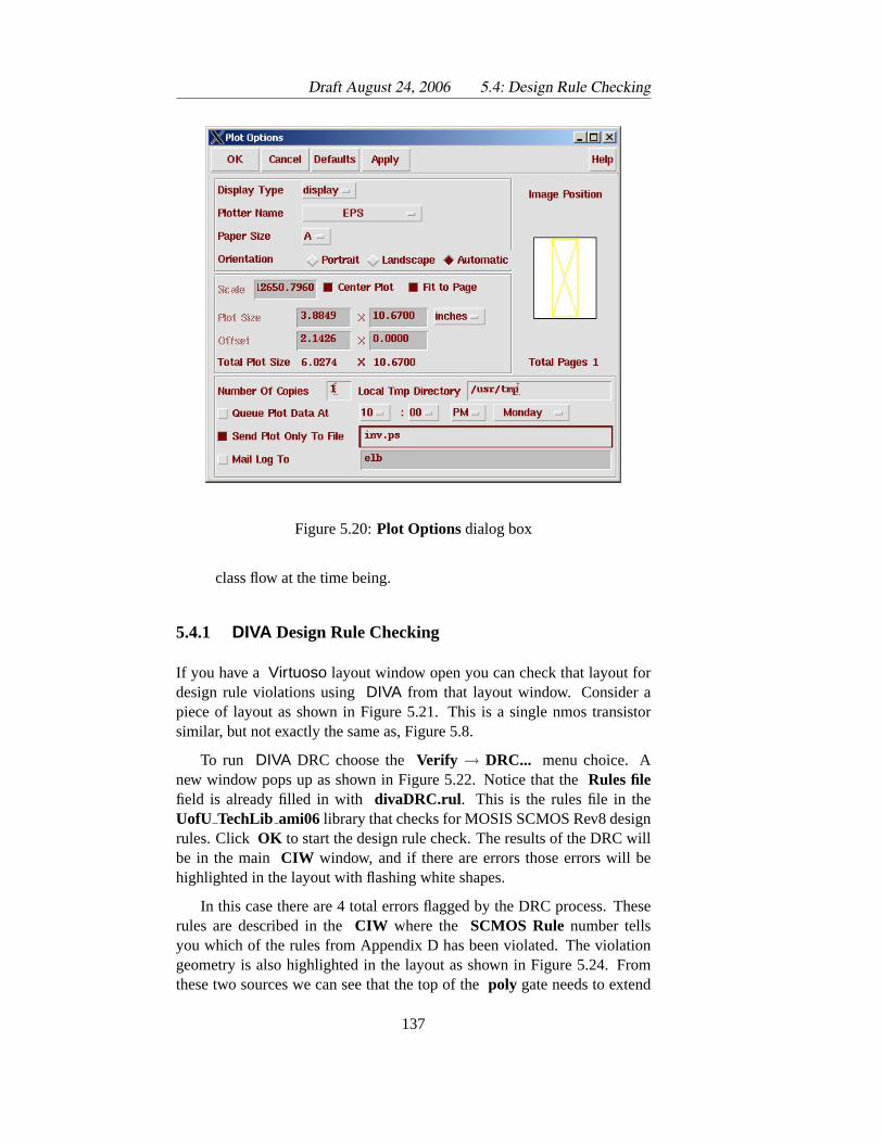
Draft August 24, 2006 5.4: Design Rule Checking
Figure 5.20:Plot Options dialog box
class flow at the time being.
5.4.1 DIVA Design Rule Checking
If you have a Virtuoso layout window open you can check that layout fordesign rule violations usingDIVA from that layout window. Consider apiece of layout as shown in Figure 5.21. This is a single nmos transistorsimilar, but not exactly the same as, Figure 5.8.
To run DIVA DRC choose theVerify → DRC... menu choice. Anew window pops up as shown in Figure 5.22. Notice that theRules filefield is already filled in with divaDRC.rul . This is the rules file in theUofU TechLib ami06 library that checks for MOSIS SCMOS Rev8 designrules. Click OK to start the design rule check. The results of the DRC willbe in the main CIW window, and if there are errors those errors will behighlighted in the layout with flashing white shapes.
In this case there are 4 total errors flagged by the DRC process. Theserules are described in theCIW where the SCMOS Rule number tellsyou which of the rules from Appendix D has been violated. The violationgeometry is also highlighted in the layout as shown in Figure 5.24. Fromthese two sources we can see that the top of thepoly gate needs to extend
137
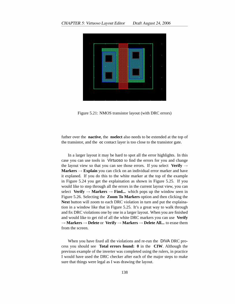
CHAPTER 5: Virtuoso Layout Editor Draft August 24, 2006
Figure 5.21: NMOS transistor layout (with DRC errors)
futher over thenactive, the nselectalso needs to be extended at the top ofthe transistor, and thecccontact layer is too close to the transistor gate.
In a larger layout it may be hard to spot all the error highlights. In thiscase you can use tools inVirtuoso to find the errors for you and changethe layout view so that you can see those errors. If you selectVerify →Markers → Explain you can click on an individual error marker and haveit explaned. If you do this to the white marker at the top of the examplein Figure 5.24 you get the explaination as shown in Figure 5.25. If youwould like to step through all the errors in the current layout view, you canselect Verify → Markers → Find... which pops up the window seen inFigure 5.26. Selecting theZoom To Markers option and then clicking theNext button will zoom to each DRC violation in turn and put the explaina-tion in a window like that in Figure 5.25. It’s a great way to walk throughand fix DRC violations one by one in a larger layout. When you are finishedand would like to get rid of all the white DRC markers you can useVerify→Markers →Deleteor Verify →Markers →Delete All... to erase themfrom the screen.
When you have fixed all the violations and re-run theDIVA DRC pro-cess you should seeTotal errors found: 0 in the CIW . Although theprevious example of the inverter was completed using the rulers, in practiceI would have used the DRC checker after each of the major steps to makesure that things were legal as I was drawing the layout.
138
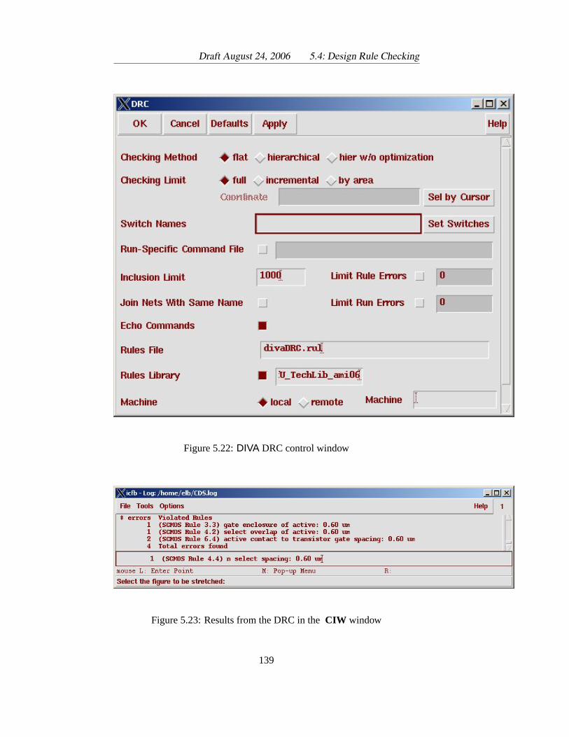
Draft August 24, 2006 5.4: Design Rule Checking
Figure 5.22:DIVA DRC control window
Figure 5.23: Results from the DRC in theCIW window
139
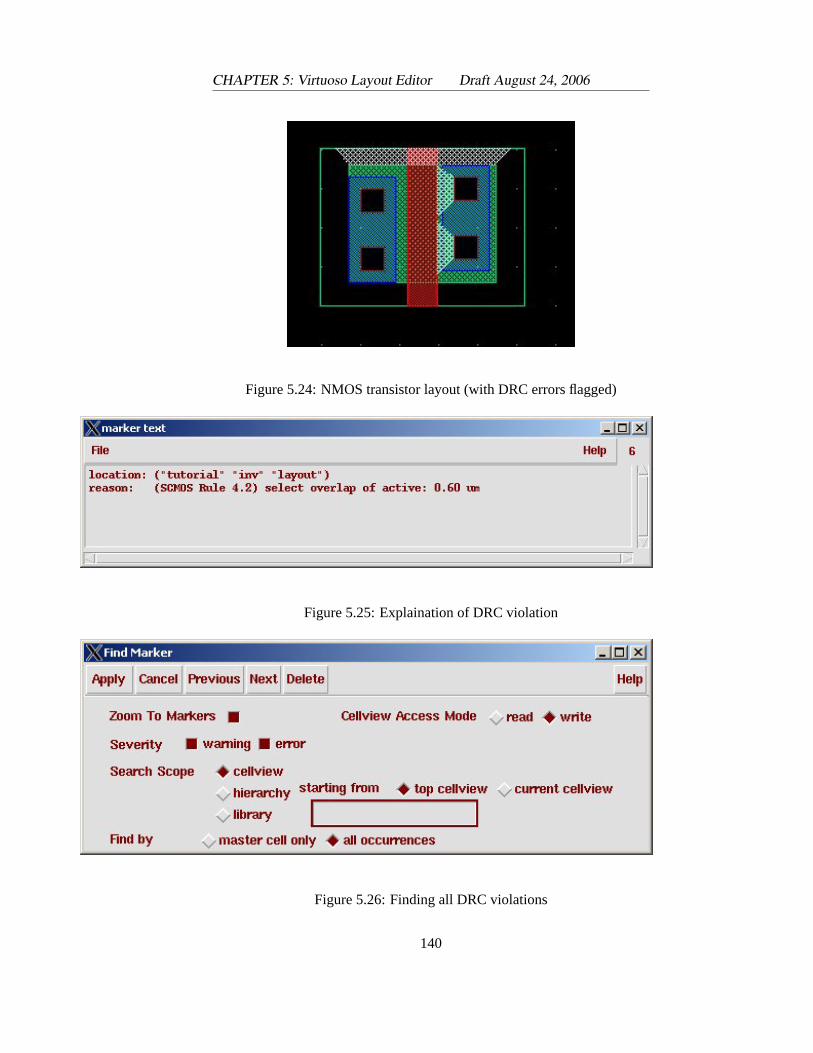
CHAPTER 5: Virtuoso Layout Editor Draft August 24, 2006
Figure 5.24: NMOS transistor layout (with DRC errors flagged)
Figure 5.25: Explaination of DRC violation
Figure 5.26: Finding all DRC violations
140
Draft August 24, 2006 5.5: Generating an Extracted View
5.5 Generating an Extracted View
Another view that is essential to the design process is anextractedview ofa cell. An extracted view is one that takes the layout view of the cell andextracts the transistor schematic from that layout. The extraction tool doesthis by knowing the electrical properties of the layers and the overlap of thelayers. For example, one of the extraction rules is that when apolysili-con rectangle overlaps a rectangle ofnactive, the area of the overlap is annmos transistor. The connection between the transistors is extracted fromthe conducting layers and the connection between those layers.
To run the excraction process usingDIVA start by opening thelayoutview of a cell (for example, the inverter from Figure 5.16). From the layoutwindow choose theVerify → Extract... menu choice. A new window popsup as shown in Figure 5.27. Notice that theRules filefield is already filledin with divaEXT.rul . This is the rules file in theUofU TechLib ami06library that extracts the transistors using the technology defined accordingto the MOSIS SCMOS Rev8 design rules. ClickOK to start the extraction.The results will show up in theicfb Command Interperter Window (CIW).Note that you should run the extractor only after passing the DRC phase. Acorrect extraction should show 0 errors as shown in Figure 5.28.
After extraction you will see that for your cell (theinv in this example) All layers in thevirtuoso layout editorare actually“layer/purpose pairs.”The “purpose” of thelayers is drawing. Thelayers in the extractedview are “net” purposeand have outline viewsto indicate this differentpurpose.
will now have a new view namedextracted. You can open this view inicfb and look at the result. For the inverter you should see outline views ofthe mask layers and transistor symbols for each of the extracted transistors.The extracted transistors will be annotated with their width and length asdefined by the rectangles that are drawn. See Figure 5.29 for an example.The extracted view is used to compare the layout with a schematic to makesure that the layout accurately captures the desired schematic. This is acritical step in the design process!
5.6 Layout Versus Schematic Checking
The process of verifying that an extracted layout captures the same tran-sistor netlist as a schematic is known asLayout versus Schematicor (LVS)checking. In order to do this check you need both aschematicview andan extracted view of the cell. Note that this LVS process will not tell youif your schematic is correct. It will only tell you if the schematic and layoutviews describe the same circuit!
To run the LVS process usingDIVA start by opening thelayout viewof a cell (for example, the inverter from Figure 5.16). From the layout win-dow choose theVerify → LVS... menu choice. A new window pops up as
141
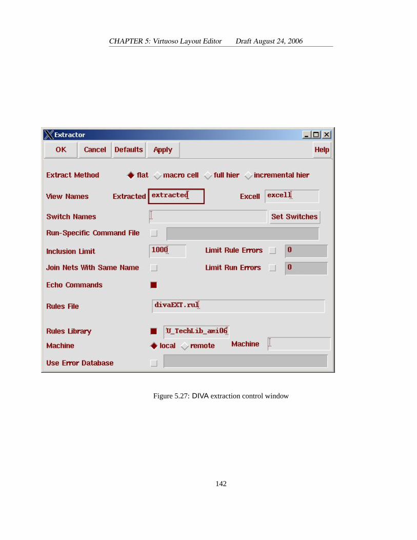
CHAPTER 5: Virtuoso Layout Editor Draft August 24, 2006
Figure 5.27:DIVA extraction control window
142
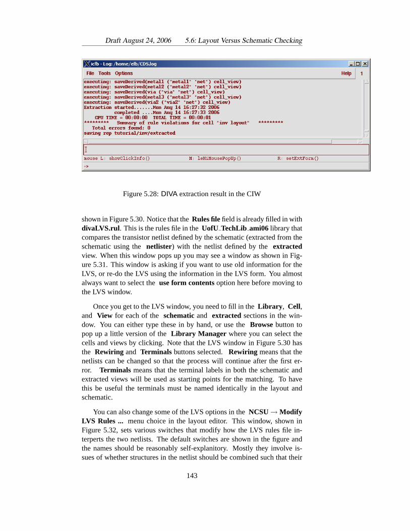
Draft August 24, 2006 5.6: Layout Versus Schematic Checking
Figure 5.28:DIVA extraction result in the CIW
shown in Figure 5.30. Notice that theRules filefield is already filled in withdivaLVS.rul . This is the rules file in theUofU TechLib ami06 library thatcompares the transistor netlist defined by the schematic (extracted from theschematic using thenetlister) with the netlist defined by theextractedview. When this window pops up you may see a window as shown in Fig-ure 5.31. This window is asking if you want to use old information for theLVS, or re-do the LVS using the information in the LVS form. You almostalways want to select theuse form contentsoption here before moving tothe LVS window.
Once you get to the LVS window, you need to fill in theLibrary , Cell,and View for each of theschematicand extracted sections in the win-dow. You can either type these in by hand, or use theBrowse button topop up a little version of theLibrary Manager where you can select thecells and views by clicking. Note that the LVS window in Figure 5.30 hasthe Rewiring and Terminals buttons selected.Rewiring means that thenetlists can be changed so that the process will continue after the first er-ror. Terminals means that the terminal labels in both the schematic andextracted views will be used as starting points for the matching. To havethis be useful the terminals must be named identically in the layout andschematic.
You can also change some of the LVS options in theNCSU→ ModifyLVS Rules ... menu choice in the layout editor. This window, shown inFigure 5.32, sets various switches that modify how the LVS rules file in-terperts the two netlists. The default switches are shown in the figure andthe names should be reasonably self-explanitory. Mostly they involve is-sues of whether structures in the netlist should be combined such that their
143
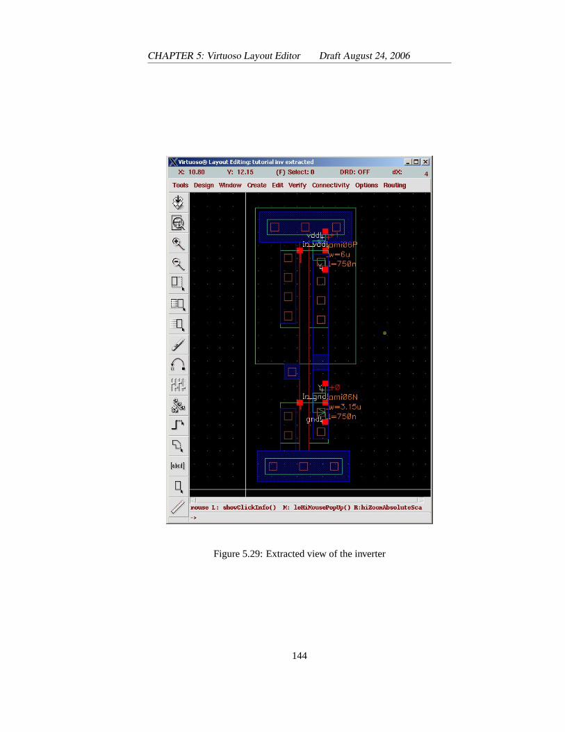
CHAPTER 5: Virtuoso Layout Editor Draft August 24, 2006
Figure 5.29: Extracted view of the inverter
144
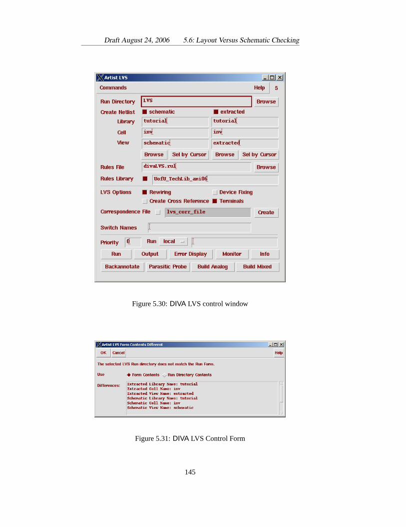
Draft August 24, 2006 5.6: Layout Versus Schematic Checking
Figure 5.30:DIVA LVS control window
Figure 5.31:DIVA LVS Control Form
145
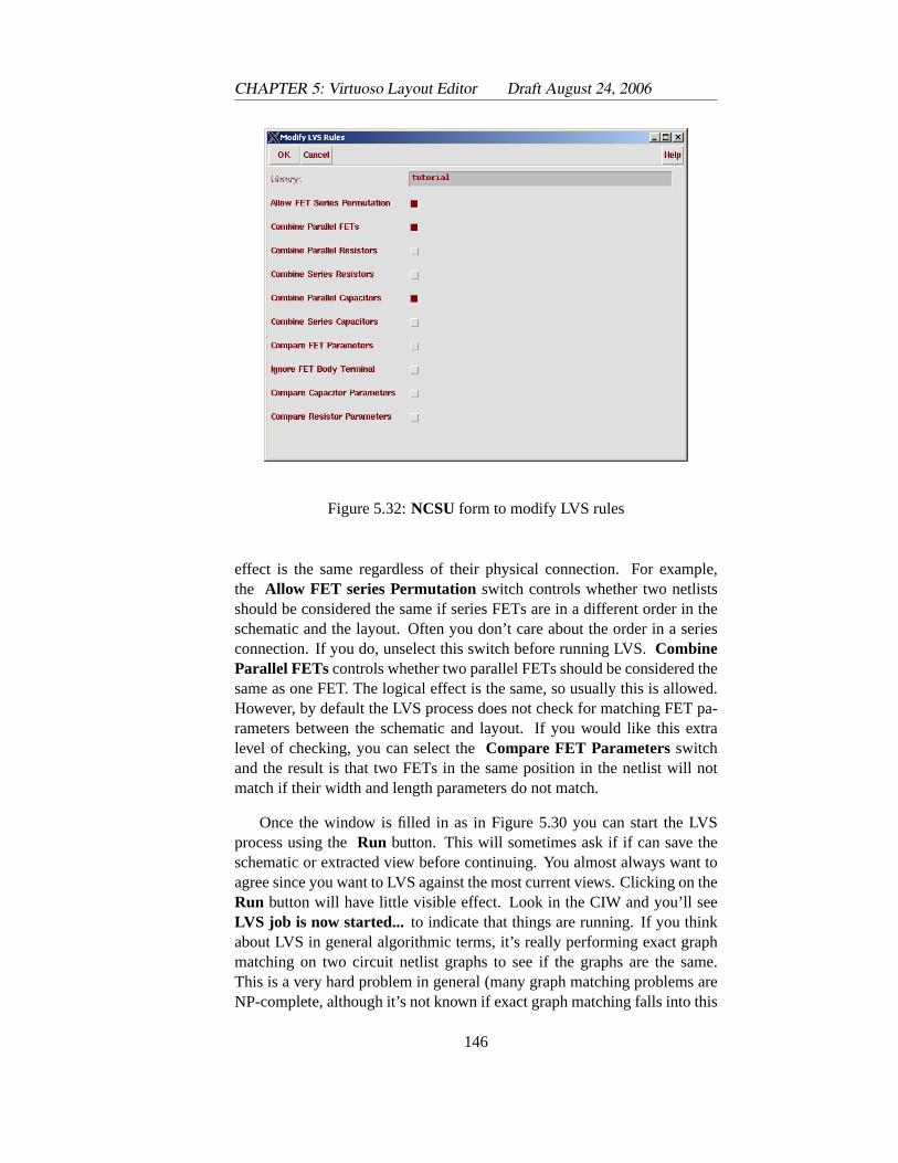
CHAPTER 5: Virtuoso Layout Editor Draft August 24, 2006
Figure 5.32:NCSU form to modify LVS rules
effect is the same regardless of their physical connection. For example,the Allow FET series Permutation switch controls whether two netlistsshould be considered the same if series FETs are in a different order in theschematic and the layout. Often you don’t care about the order in a seriesconnection. If you do, unselect this switch before running LVS.CombineParallel FETs controls whether two parallel FETs should be considered thesame as one FET. The logical effect is the same, so usually this is allowed.However, by default the LVS process does not check for matching FET pa-rameters between the schematic and layout. If you would like this extralevel of checking, you can select theCompare FET Parametersswitchand the result is that two FETs in the same position in the netlist will notmatch if their width and length parameters do not match.
Once the window is filled in as in Figure 5.30 you can start the LVSprocess using theRun button. This will sometimes ask if if can save theschematic or extracted view before continuing. You almost always want toagree since you want to LVS against the most current views. Clicking on theRun button will have little visible effect. Look in the CIW and you’ll seeLVS job is now started... to indicate that things are running. If you thinkabout LVS in general algorithmic terms, it’s really performing exact graphmatching on two circuit netlist graphs to see if the graphs are the same.This is a very hard problem in general (many graph matching problems areNP-complete, although it’s not known if exact graph matching falls into this
146
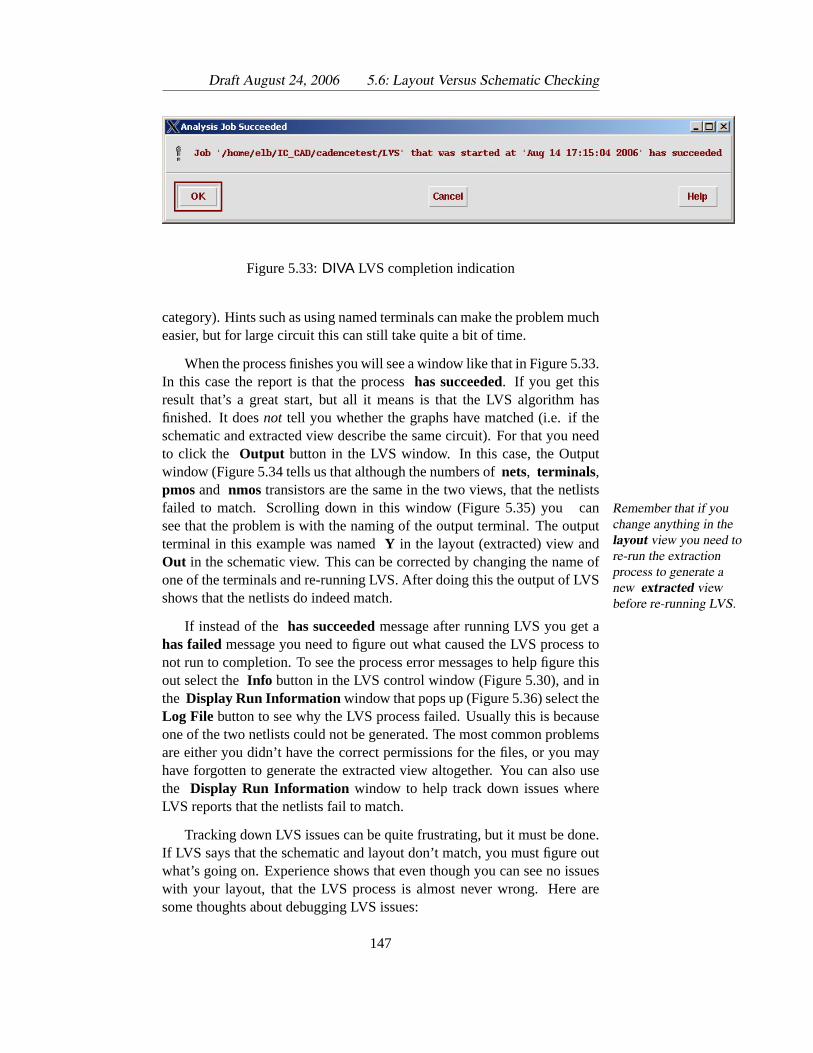
Draft August 24, 2006 5.6: Layout Versus Schematic Checking
Figure 5.33:DIVA LVS completion indication
category). Hints such as using named terminals can make the problem mucheasier, but for large circuit this can still take quite a bit of time.
When the process finishes you will see a window like that in Figure 5.33.In this case the report is that the processhas succeeded. If you get thisresult that’s a great start, but all it means is that the LVS algorithm hasfinished. It doesnot tell you whether the graphs have matched (i.e. if theschematic and extracted view describe the same circuit). For that you needto click the Output button in the LVS window. In this case, the Outputwindow (Figure 5.34 tells us that although the numbers ofnets, terminals,pmosand nmos transistors are the same in the two views, that the netlistsfailed to match. Scrolling down in this window (Figure 5.35) you canRemember that if you
change anything in thelayout view you need tore-run the extractionprocess to generate anew extracted viewbefore re-running LVS.
see that the problem is with the naming of the output terminal. The outputterminal in this example was namedY in the layout (extracted) view andOut in the schematic view. This can be corrected by changing the name ofone of the terminals and re-running LVS. After doing this the output of LVSshows that the netlists do indeed match.
If instead of the has succeededmessage after running LVS you get ahas failedmessage you need to figure out what caused the LVS process tonot run to completion. To see the process error messages to help figure thisout select theInfo button in the LVS control window (Figure 5.30), and inthe Display Run Information window that pops up (Figure 5.36) select theLog File button to see why the LVS process failed. Usually this is becauseone of the two netlists could not be generated. The most common problemsare either you didn’t have the correct permissions for the files, or you mayhave forgotten to generate the extracted view altogether. You can also usethe Display Run Information window to help track down issues whereLVS reports that the netlists fail to match.
Tracking down LVS issues can be quite frustrating, but it must be done.If LVS says that the schematic and layout don’t match, you must figure outwhat’s going on. Experience shows that even though you can see no issueswith your layout, that the LVS process is almost never wrong. Here aresome thoughts about debugging LVS issues:
147
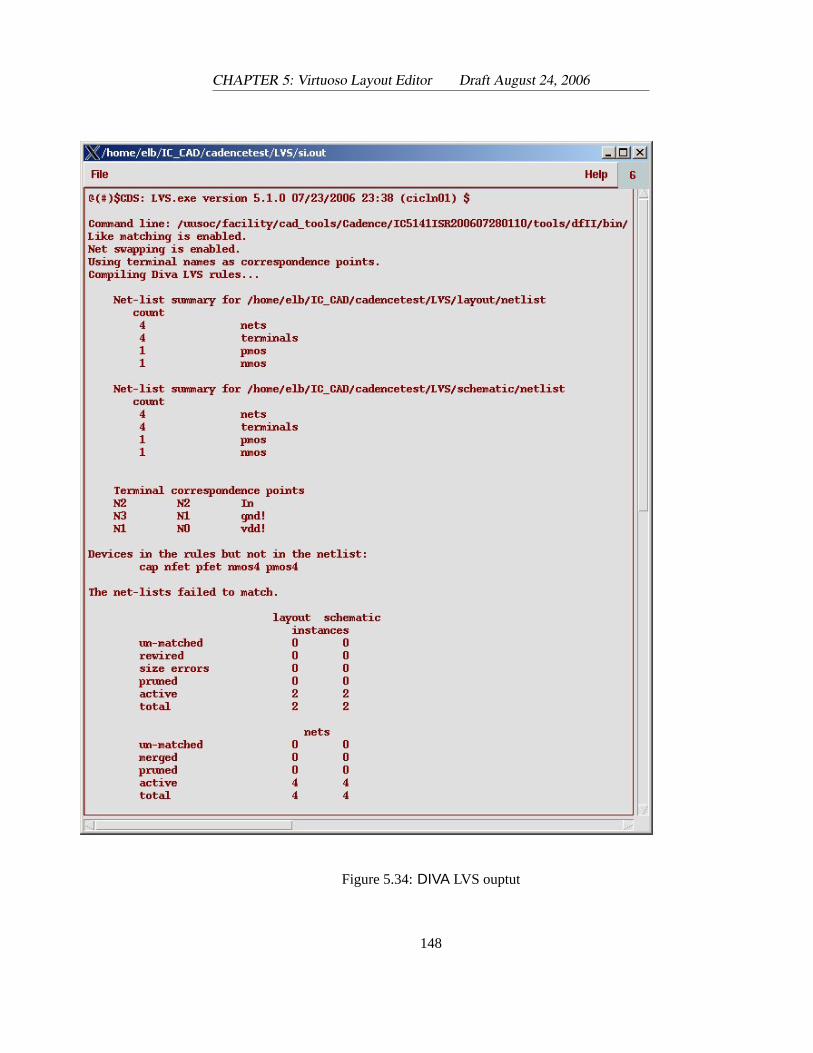
CHAPTER 5: Virtuoso Layout Editor Draft August 24, 2006
Figure 5.34:DIVA LVS ouptut
148
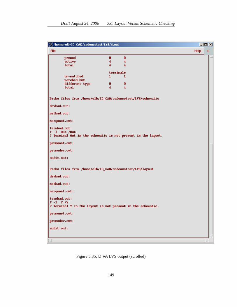
Draft August 24, 2006 5.6: Layout Versus Schematic Checking
Figure 5.35:DIVA LVS output (scrolled)
149
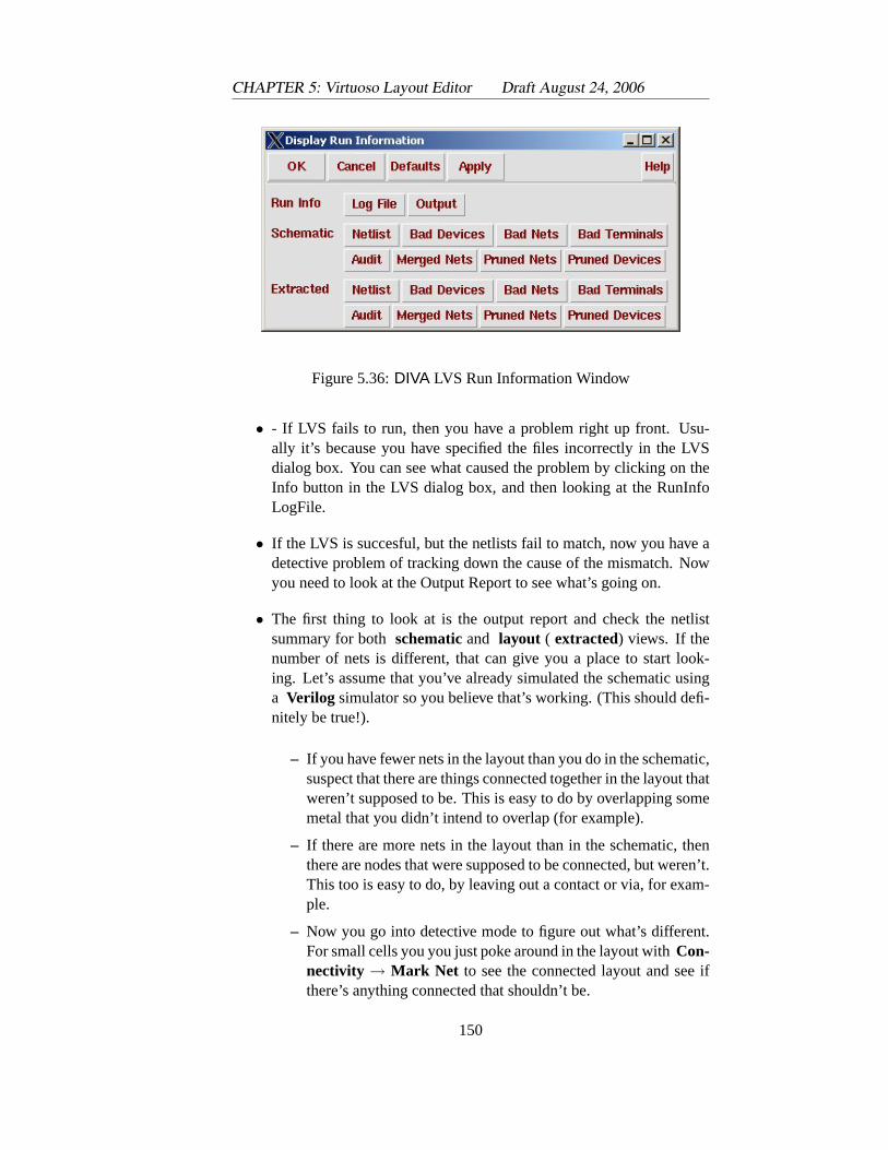
CHAPTER 5: Virtuoso Layout Editor Draft August 24, 2006
Figure 5.36:DIVA LVS Run Information Window
• - If LVS fails to run, then you have a problem right up front. Usu-ally it’s because you have specified the files incorrectly in the LVSdialog box. You can see what caused the problem by clicking on theInfo button in the LVS dialog box, and then looking at the RunInfoLogFile.
• If the LVS is succesful, but the netlists fail to match, now you have adetective problem of tracking down the cause of the mismatch. Nowyou need to look at the Output Report to see what’s going on.
• The first thing to look at is the output report and check the netlistsummary for bothschematicand layout ( extracted) views. If thenumber of nets is different, that can give you a place to start look-ing. Let’s assume that you’ve already simulated the schematic usinga Verilog simulator so you believe that’s working. (This should defi-nitely be true!).
– If you have fewer nets in the layout than you do in the schematic,suspect that there are things connected together in the layout thatweren’t supposed to be. This is easy to do by overlapping somemetal that you didn’t intend to overlap (for example).
– If there are more nets in the layout than in the schematic, thenthere are nodes that were supposed to be connected, but weren’t.This too is easy to do, by leaving out a contact or via, for exam-ple.
– Now you go into detective mode to figure out what’s different.For small cells you you just poke around in the layout withCon-nectivity → Mark Net to see the connected layout and see ifthere’s anything connected that shouldn’t be.
150
Draft August 24, 2006 5.6: Layout Versus Schematic Checking
– You can also open the extracted layout and look at things there.The advantage of this is that the extracted layout has the netlistalready constructed so when you select something you’re select-ing the whole connected layout net by default. You can also useq with the selected net to see thing like net number of the se-
lected net.
• You can also use the error reporting mechanism in LVS to see whichnets are different. After running LVS, open a schematic window andan extracted view window for the cell in question. Now click on theError Display button in the LVS dialog box. This will let you walkthrough the errors in the LVS output file one at a time and will high-light in the schematic or the extrated view which node that error istalking about. This can be very helpful if you have only a few errorsin the output file, but can also be more confusing than helpful if youhave a lot of errors. This is because once you have one error, it cancause lots of things to look like errors. This can, however, be a goodway to see that the output file is talking about, and you might walkthrough the errors and see a big connected net in the layout that youthought should be two separate nodes (for example).
• If you’d like to look at the extracted view and search for a particu-lar net, you can do it through a slightly non-obvious procedure. Ofcourse, you can use theError Display to step through the errors un-til you get to the one with the net you’re interested in. Or you canopen the extractred view, selectVerify → Shorts. Dismiss the in-formational dialog box to get theShorts Locator box. Type the netname or number in theNet Namebox and click onRun. This willhighlight that node in orange. ClickFinish to start over with anothernet. Clearly this dialog box does something more interesting than justhighlight a net. It has something to do with tracking down shorts be-tween nets, but I have to admit I don’t know exactly what it does. Ido know that it highlights nets by name in extracted views!
• Remember that a single LVS error can cause lots of things to look likeerrors. Once you find one error, rerun LVS and see what’s changed.A single fix can cause lots of reported violations to go away.
• If all else fails and you’re convinced that things are correct, try re-moving the /IC CAD/cadence/LVSdirectory and re-running LVS.It’s possible (but rare) that you mess LVS up so badly that you needto delete all its generated files and start over.
If your cell passes LVS then it’s a pretty good indication that your layoutis a correctly functioning circuit that matches the behavior of the transistorschematic.
151
CHAPTER 5: Virtuoso Layout Editor Draft August 24, 2006
5.6.1 Generating an analog-extracted view
The LVS process compares theschematicview with the extractedview tosee if the netlists are the same. Once LVS says that the netlists are the same,there is one further step that you can take. Click on theBuild Analog buttonin the LVS control window (Figure 5.30). Make sure toInclude All theextracted paracitics so that if you extracted paracitic capaciters they willbe included, and clickOK . This will generate yet anotherCell View calledanalog-extracted. This view is very similar to theextracted view, but hasadditional power supply information so that the view can be simulated withthe analog simulatorSpectre. This will be seen in Chapter 6.
5.6.2 Overall Cell Design Flow (so far...)
The complete cell design flow involves each of the steps defined previously.They are:
1. Start with a schematic of your desired circuit. The schematic can bemade using components from theUofU Digital v1 1 library and thetransistors from theNCSU Analog Parts and UofU Analog Partslibraries. UseComposer as described in Chapter 3.
2. Simulate that schematic using one of the Verilog simulators definedin Chapter 4 to make sure the functionality is waht you want. Makesure to use a self-checking testbench.
3. Now draw a layout of the cell using theVirtuoso as described in thisChapter.
4. Make sure that thelayout view passes DRC.
5. Generate anextractedview.
6. Make sure that theschematicand extracted view match by usingthe LVS checker.
7. Generate theanalog-extractedcell view for later analog simulation.
5.7 Standard Cell Template
Designing a standard cell library involves creating a set of cells (gates, flipflops, etc.) that work together throughout the CAD tool flow. In general thismeans that the cells should have all the views necessary for designing withthe cells, and should be compatable in terms of their attributes so that they
152
Draft August 24, 2006 5.7: Standard Cell Template
can all work together. At this point in out understanding of the CAD flowthis means that each cell in the cell library needs the following views:
schematic: This view defines the gate or transistor level definition of thecell. It can be simulated using any of the Verilog simulators in Chap-ter 4 as a switch-level or a behavioral-level simulation.
behavioral: This view is the Verilog description of the cell. It should in-clude both behavior andspecifyblocks for timing so that the timingcan be back-annotated with better estimates as the design progressesthrough the flow.
layout: This view describes the mask layout of the cell. It should pass allDRC checks. It should also follow strict physical and geometricalstandards so that the cells will fit with each other and work together(the subect of this Section).
extracted: This view extracts the circuit netlist from the layout and is gen-erated by the extraction process. It should be used with the LVSchecker to verify that thelayout and schematicviews represent thesame circuit.
analog-extracted: This view is an augmented version of theextractedview that includes information so it can be used by the analog simula-tor Spectre. It is generated from the extracted view through the LVSprocess.
In addition to these views, subsequent Chapters in this text will intro-duce a number of additional views that are required for the final, completecell library. They include:
abstract: This is a view that is derived from the layout. It tells the placeand route tool where the ports of the cell are, and where the “keep-outs” or obstructions of the cell are that it should not try to route over.Generating this view from the layout is described in Chapter 9.
LEF: This is a Library Exchange Format file that is derived from the ab-stract view of the cell and is read by the place and route tool (SOCEncounter) so that it can get information about the technology thatit is routing in, and about the abstract views of the cells in the library.This view is also generated by theAbstract program.
Verilog Interface: The system you design will eventually be input to theplace and route tool as a structural verilog file that describes the stan-dard cell gates used in your design and the connections between them.
153
CHAPTER 5: Virtuoso Layout Editor Draft August 24, 2006
In addition to this file you need a simple I/O interface of each cell(separate from the LEF file) so that the place and route tool can parsethe structural verilog file. This will also be described in Chapter 9.
Lib: This is a standard format, calledLiberty format (usually with a.libfilename extension), for describing cells so that the synthesis toolscan understand the cells. The file describes the I/O interface, the logicfunction, the capacitance on the cell pins, and extracted timing for thecell. This file can be generated by hand, using analog simulation usingSpectre or Spice, or using theSignalStorm tool from Cadenceand will be described in Chapter 7.
5.7.1 Standard Cell Geometry Specification
In standard cell based design flow, the automatic place and route tool (SOCEncounter in this flow) places the standard cells selected by the synthesisengine (Synopsys design compiler or Cadence BuildGates) in a setof rows. To make this packing as efficient as possible we can plan our cellsso that they can be placed adjacent to each other. With some simple rulesabout how the internal layout of the cells is designed, we can guarantee thatany two cells can be placed next to each other without causing any DRCviolations. Some overall design considerations are:
• Since the cells are going to be placed in rows adjacent to each otherwe will make all our cells the same height so that they fit nicely intorows.
• All our CMOS based standard cells have a set ofpmos transistors inan nwell for the pull-up network andnmos transistors for the pull-down network. We will always place thenwell with pmostransistorson top of the layout andnmos transistors at the bottom. By doingthis and having the same height in thenwell layer for all cells, wecan have a continuous well throughout the row of cells.
• All standard cells have a power and ground bus. To avoid shortingof power and ground while placing cells adjacent to each other, weplace the vdd! bus on top andgnd! bus at the bottom of the cell(which makes sense because we have the pull up network on top andpull down at the bottom). Having equal heights for these buses for allcells and running these buses throughout the width of the cells allowfor automatic connection of adjacent cell power and ground buses byabutment.
• All the standard cell layouts will have a fixed origin in the lower leftcorner of the layout, but pay attention, it is not the absolute lower left
154
Draft August 24, 2006 5.7: Standard Cell Template
of the layout!
Hence we define the following standard cell dimensions for class cellsthat will be implemented in the AMI C5N0.5µ CMOS process.
Cell height = 27 microns. This height is measured from the center of thegnd! bus to the center of thevdd! bus.
Cell width = multiple of 2.4 microns. This matches the verticalmetal2routing pitch and also the pitch of theNTAP and SUBTAP well andsubstrate contacts.
nwell height from top of cell = 15.9 microns. This is 2/3 of the cell heightbecausepmostransistors are usually made wider thannmostransis-tors.
vdd! and gnd! bus height = 2.4 microns.This height is centered on thesupply lines so that 1.2 microns is above the cell boundary and 1.2microns is below the cell boundary. This way if the cells are abuttedvertically with the supply lines overlapping those supply lines remain2.4 microns wide.
vdd! and gnd! bus width = 1.2 microns overhang beyond the cell boundary.This is for convenience so that themetal1 layer of the well and sub-strate contacts can overlap the cells safely.
Based on thenwell size and placement, and the MOSIS SCMOS rules,we can now standardize thenselectand pselectsizes as well. The closestthat select edges can be to the well edges is 1.2 microns (SCMOS rules 2.3and 4.2). So, the select restrictions are:
pselect height from inner edge of vdd! bus = 13.5 microns
nselect height from inner edge of gnd! bus = 8.7 microns
nselect and pselect width = cell width
nwell overhang outside cell width = 1.5 microns(to top, left and right ofthe cell)
To avoidlatch-up in the circuit we place substrate and well contacts tomake sure that thenwell is tied to vdd and the substrate is tied to gnd. Asseen in Section 5.2, we use predefined contacts for these connections inThe usual rule of thumb
for the minimumnumber of well contactsis to place one wellcontact for every squareof well material.
the form of NTAP and SUBTAP contacts. Each of these contacts is 2.4microns wide so you can think of the overall cell width as a multiple of 2.4
155
CHAPTER 5: Virtuoso Layout Editor Draft August 24, 2006
microns, or as an integer number ofNTAP and SUBTAP cells. Thesecontacts are placed centered on thevdd! and gnd! lines. Note that placingthis many well and substrate contacts is overkill, but does not have negativeeffects.
It’s a good idea to builr a standard cell layouttemplate incorporatingthese basic design specifications. This can serve as a starting point for thedesign of new cells. It’s also a good idea to keep your library cells in aseparateCadence library from your designs. This keeps the distinctionclear between the library cells and the designs that use those cells. Youcould, for example, make a template with thegnd! bus on the bottom,including the SUBTAP contacts, thevdd! bus on the top, including theNTAP contacts, and thenwell, nselect, and pselect layers as definedearlier. An example of such a template with rulers showing the dimensions,and examplepmosand nmostransistors is shown in Figure 5.37. This cell,even without actual connections between the transistors, should pass DRCwith no violations.
The notion of acell boundary was used without specific definition inthe preceeding text. The cell boundary is the rectangle that defines theThe cell boundary will
be generated as arectangle of typeprBound by the
Abstract program. Thislayer is not editable by
default, but can beenabled if needed
through the LSWwindow.
outline of the cell from the place and route tool’s point of view. We havedefined our library so that the cell boundary is actually inside of the celllayout geometry so that when the cells are abutted with respect to the cellboundary, they actually overlap by a small amount. The cell boundary isshown in Figure 5.38, but you don’t have to draw it by hand. It will bederived during the process of extracting anabstract view as described inChapter 9.
In order to make sure that there will not be any DRC violations whencells are abutted, it is very important that no geometry on any layers (otherthan the layers already in the template) falls within 0.6 microns from theleft and right of the cell boundary or within the vdd! or gnd! buses.This rule is in addition to to other SCMOS Design Rules within the cell andapplies even if the DRC of the individual standard cell does not complain.For example, in the layout shown in Figurr 5.38, thenactive and pactivelayers are placed0.6µ away from the cell boundaries on left and right side.They cannot come any closer to the boundary. Also, in thelayout viewshown, the pmos and nmos transistor gates (poly layer) are placed justtouching the vdd! and gnd! bus inner edges. The gates could go fartheraway from the bus inner edges but cannot extend into the bus structure. Ifyou need more space than these rules allow, you will have to make yourwhole cell wider. Each time you make a cell wider, it has to be made widerin increments of2.4µ.
156
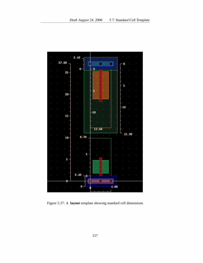
Draft August 24, 2006 5.7: Standard Cell Template
Figure 5.37: A layout template showing standard cell dimensions
157
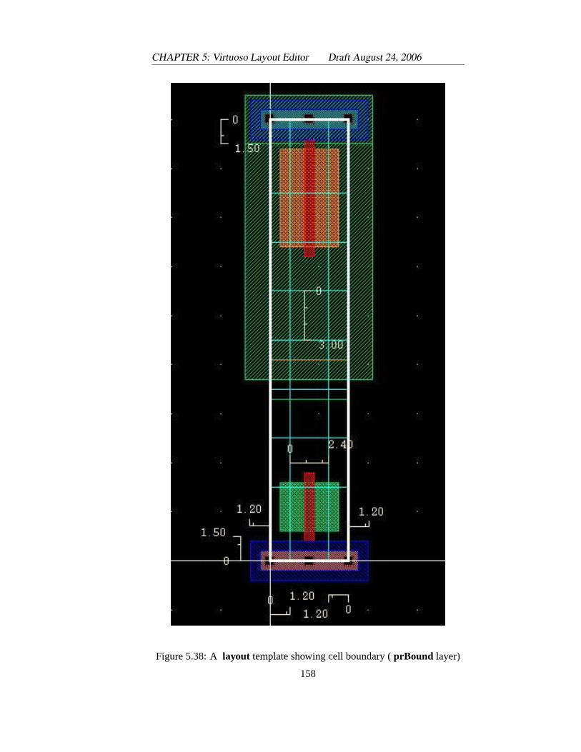
CHAPTER 5: Virtuoso Layout Editor Draft August 24, 2006
Figure 5.38: A layout template showing cell boundary (prBound layer)
158
Draft August 24, 2006 5.7: Standard Cell Template
5.7.2 Standard Cell I/O Pin Placement
The design rules for a specific VLSI process define the minimum dimen-sions and spacing for all layers, including the metal layers that are used forrouting signals. The minimum spacing between two metal routing layersis called thepitch of that layer. It’s also more efficient for overall wiringdensity if the metal wiring on each layer of metal is restricted to a single di-rection. This is well known by people who make multi-layer printed circuitboards and the principle is the same for VLSI chips. In our case we willeventually tell the place and router to prefer horizontal direction routing forlayers metal1and metal3, and vertical routing for layermetal2. The pitchfor metal2 vertical routing according to the MOSIS SCMOS design rulesis 2.4µ which, conveniently (but not coincidentally), matches our standardcell dimension increment and well and substrate contact width. Themetal3routing pitch is3.0µ and so sets the routing pitch for all horizontal routingby the place and route tool even thoughmetal1can actually be routed on afiner pitch when routed by hand.
It turns out to make the job of the place and route tool much easier if theconnection points to the cell are centered on horizontal and vertical routingpitch dimensions. The grid lines in Figure 5.38 (actually 0-width rectanglesof type wire in the layout) show the horizontal and vertical routing chan-nels in the cell. We follow offset grid line placement rules where the gridlines are offset by half of the vertical and horizontal grid line pitch fromthe origin. Thus the vertical grid lines start at1.2µ from the y-axis and Remember to use shape
pins for all connectionpins in a cell.
are spaced2.4µ thereafter. Similarly, the horizontal grid lines start at1.5µfrom the x-axis and are spaced3.0µ thereafter. However it should be notedthat the first and last horizontal grid lines cannot be used, as any geome-try placed on them extends into thevdd! or gnd! bus violating the rulesdefined above.
Input and ouptut pins for a cell should be placed at the intersection of thehorizontal and vertical routing channels if at all possible. Also, if possible,do not place two pins on the same vertical or horizontal routing channel.For our cells it is most efficient if all cell I/O pins are made inmetal2. Thismakes it easy for the router to jump over thevdd! and gnd! buses to makecontact with the pin using ametal2vertical wire.
As far as possible use onlymetal1 for signal routing within the stan-dard cell layout. Routing onmetal2 layer can be used if necessary, but ifit is used it should always run centered on a vertical routing channel lineand never run horizontally except for very short distances (this is to reducemetal2 blockage layers enabling easier place and route). In any case, makesure that there are no horizontal metal2 runs around I/O pins. You should tryto avoid any use ofmetal3 in your library cells. That routing layer shouldbe reserved for use by the place and route tool. I know of at least one com-
159
CHAPTER 5: Virtuoso Layout Editor Draft August 24, 2006
mercial standard cell library for a three-metal process like ours that containsover 400 cells and uses onlymetal1 in the cells (other than the1.2µ by1.2µ metal2connection pins) so it is possible to define lots of cells withoutusing more than one metal layer.
5.7.3 Standard Cell Transistor Sizing
For critical designs MOSIS recommends the minimum transistor width tobe1.5µ for the AMI C5N process. The minimum transistor length for AMIC5N process is0.6µ. Hence the minimum dimension for annmos transis-tor pulling the output directly tognd! is W/L = 1.5µ/0.6µ. TO roughlyequalize the strength of the pullup and pulldowns the minimum dimensionof a pmos transistor pulling the output directly tovdd! should be W/L =3.0µ/0.6µ. For series stack of transistors between output andvdd! orThe 2:1 width ratio
roughly compensates forthe mobility of majority
carriers in pmostransistors (holes) whichis roughly half of that ofnmos transistor carriers
(electrons).
gnd!, the transistor width should be the number of transistors in the stackmultiplied by the minimum width for a single transistor stack. If you can’tmake the series transistors quite wide enough, at least do your best. Also, astack greater than four should not be used. For example, if there are threepmostransistors in a series stack between output node andvdd!, then thesetransistors will be sized W/L =(3× 3.0)µ/0.6µ = 9.0µ/0.6µ if possible.
You can also create cells with different drive strengths by adjusting thewidth of the output transistors. For example, an inverter with a1.5µ pull-A 2x inverter has extra
output drive, but alsoextra input capacitance,so the resulting logicaleffort is the same, butthe electrical effort is
different.
down and3.0µ pullup could be considered a 1x inverter, and one with a3.0µ pulldown and6.0µ pullup would then be a 2x inverter denoting that itsoutput drive is two times as strong as the 1x inverter.
A standard cell template for a cell that is four contacts wide is shownin Figure 5.39. The standard 1x inverter from theUofU Digital v1 1 celllibrary is shown in Figurefig:inv1x, and the 1x two-input nand gate fromthat library is shown in Figure 5.41.
160
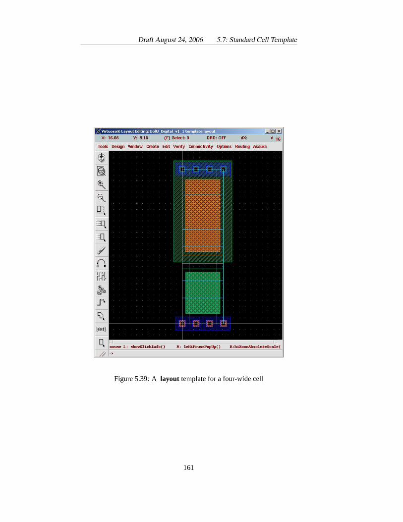
Draft August 24, 2006 5.7: Standard Cell Template
Figure 5.39: A layout template for a four-wide cell
161
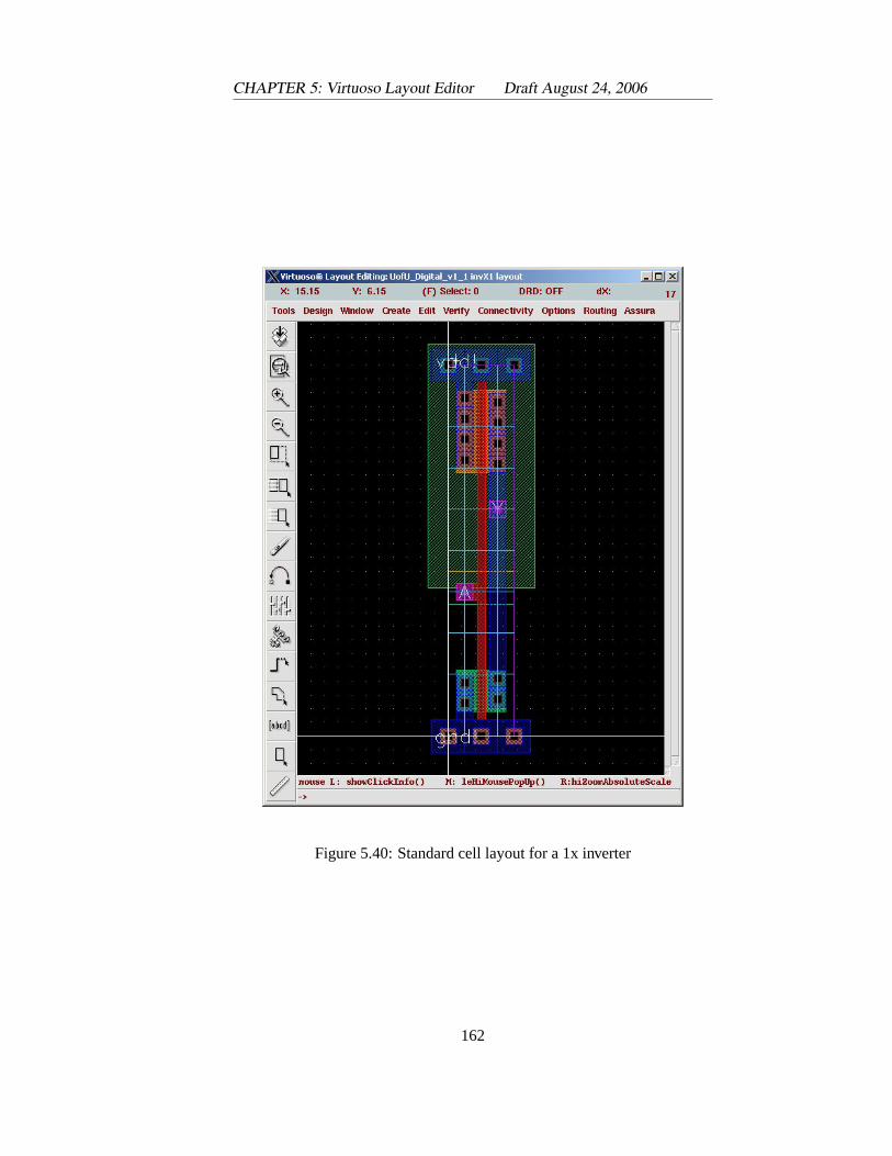
CHAPTER 5: Virtuoso Layout Editor Draft August 24, 2006
Figure 5.40: Standard cell layout for a 1x inverter
162
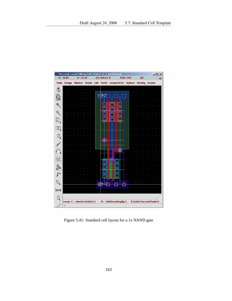
Draft August 24, 2006 5.7: Standard Cell Template
Figure 5.41: Standard cell layout for a 1x NAND gate
163

CHAPTER 5: Virtuoso Layout Editor Draft August 24, 2006
164
Chapter 6
Spectre Analog Simulator
THE SIMULATION described in Chapter 4 is eitherbehavioral simula-tion where the Verilog describes high-level behaviors in a software-like style, orswitch level simulation where the circuit is expanded
all the way to transistors that are modeled as perfect switches using built-inVerilog transistor-switch models. A more accurate simulation would try tomodel the transistors as analog devices and use as much detail as possibleThe FORTRAN history
of Spice is why eventoday the input files foranalog simulators arecalled “spice decks.”That term goes back tothe punched card decksthat were used for inputto these FORTRANprograms.
in that analog model to as accurately as possible reflect the real electricalbehavior of the transistor network. Analog simulators of this sort can gen-erally trace their background to a simulator calledSpice that was origi-nally developed at Berkeley in the early 1970’s. Through the early 1980’sSpice was still written in FORTRAN, and you can actually still obtain theSpice2G6 FORTRAN code from Berkeley if you look around carefullyenough. Spice3 was the first C-language version in 1985. Since escap-ing from Berkeley there have been many commercial versions of Spice andSpice-like programs includingHspice, Pspice, IS Spice, and Micro-cap.
The analog simulator integrated into theCadence framework is calledSpectre. It is similar to Spice in terms of simulating the analog behaviorof the transistors, and it even accepts “spice decks” as input in addition toit’s own Spectre format. It operates slightly differently internally and isclaimed to be a little faster thanSpice. From your point of view they areessentially identical simulators though. They take the same input decks andproduce the same waveform outputs that show the analog behavior of thecircuit network.
An important thing to keep in mind is that while the Verilog simulationsused abstract logical 0 and 1 signals for inputs and outputs, analog simula-tions with Spectre will use analog voltages for inputs and outputs. Thus,you now need to be concerned with things like what voltage the power sup-
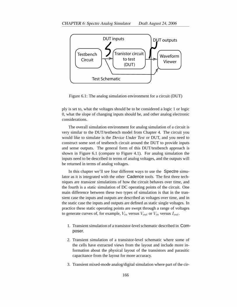
CHAPTER 6: Spectre Analog Simulator Draft August 24, 2006
Tranistor circuitto test (DUT)
Test Schematic
Waveform Viewer
DUT inputs DUT outputs
TestbenchCircuit
Figure 6.1: The analog simulation environment for a circuit (DUT)
ply is set to, what the voltages should be to be considered a logic 1 or logic0, what the slope of changing inputs should be, and other analog electronicconsiderations.
The overall simulation environment for analog simulation of a circuit isvery similar to the DUT/testbench model from Chapter 4. The circuit youwould like to simulate is theDevice Under Test or DUT, and you need toconstruct some sort of testbench circuit around the DUT to provide inputsand sense outputs. The general form of this DUT/testbench approach isshown in Figure 6.1 (compare to Figure 4.1). For analog simulation theinputs need to be described in terms of analog voltages, and the outputs willbe returned in terms of analog voltages.
In this chapter we’ll see four different ways to use theSpectre simu-lator as it is integrated with the otherCadence tools. The first three tech-niques aretransient simulations of how the circuit behaves over time, andthe fourth is astatic simulation of DC operating points of the circuit. Onemain difference between these two types of simulation is that in the tran-sient case the inputs and outputs are described as voltages over time, and inthe static case the inputs and outputs are defined as static single voltages. Inpractice these static operating points are swept through a range of voltagesto generate curves of, for example,Vin versusVout or Vin versusIout.
1. Transient simulation of a transistor-level schematic described inCom-poser.
2. Transient simulation of a transistor-level schematic where some ofthe cells have extracted views from the layout and include more in-formation about the physical layout of the transistors and parasiticcapacitance from the layout for more accuracy.
3. Transient mixed-mode analog/digital simulation where part of the cir-
166
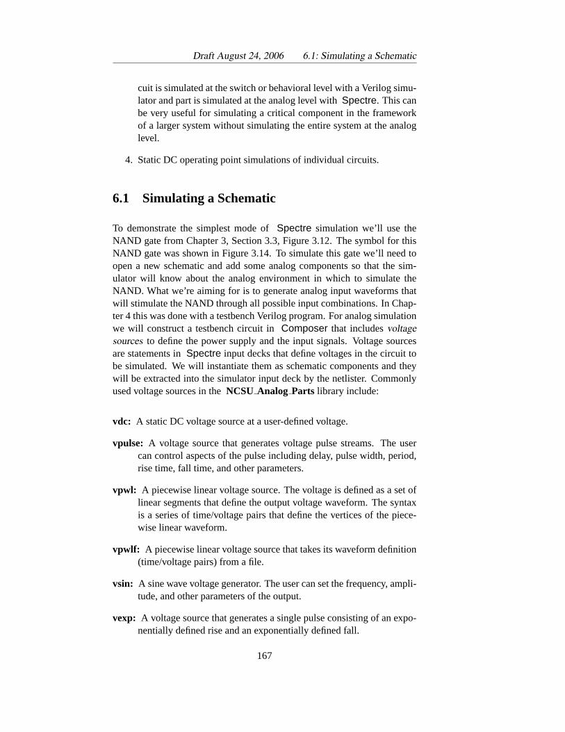
Draft August 24, 2006 6.1: Simulating a Schematic
cuit is simulated at the switch or behavioral level with a Verilog simu-lator and part is simulated at the analog level withSpectre. This canbe very useful for simulating a critical component in the frameworkof a larger system without simulating the entire system at the analoglevel.
4. Static DC operating point simulations of individual circuits.
6.1 Simulating a Schematic
To demonstrate the simplest mode ofSpectre simulation we’ll use theNAND gate from Chapter 3, Section 3.3, Figure 3.12. The symbol for thisNAND gate was shown in Figure 3.14. To simulate this gate we’ll need toopen a new schematic and add some analog components so that the sim-ulator will know about the analog environment in which to simulate theNAND. What we’re aiming for is to generate analog input waveforms thatwill stimulate the NAND through all possible input combinations. In Chap-ter 4 this was done with a testbench Verilog program. For analog simulationwe will construct a testbench circuit inComposer that includesvoltagesources to define the power supply and the input signals. Voltage sourcesare statements inSpectre input decks that define voltages in the circuit tobe simulated. We will instantiate them as schematic components and theywill be extracted into the simulator input deck by the netlister. Commonlyused voltage sources in theNCSU Analog Parts library include:
vdc: A static DC voltage source at a user-defined voltage.
vpulse: A voltage source that generates voltage pulse streams. The usercan control aspects of the pulse including delay, pulse width, period,rise time, fall time, and other parameters.
vpwl: A piecewise linear voltage source. The voltage is defined as a set oflinear segments that define the output voltage waveform. The syntaxis a series of time/voltage pairs that define the vertices of the piece-wise linear waveform.
vpwlf: A piecewise linear voltage source that takes its waveform definition(time/voltage pairs) from a file.
vsin: A sine wave voltage generator. The user can set the frequency, ampli-tude, and other parameters of the output.
vexp: A voltage source that generates a single pulse consisting of an expo-nentially defined rise and an exponentially defined fall.
167
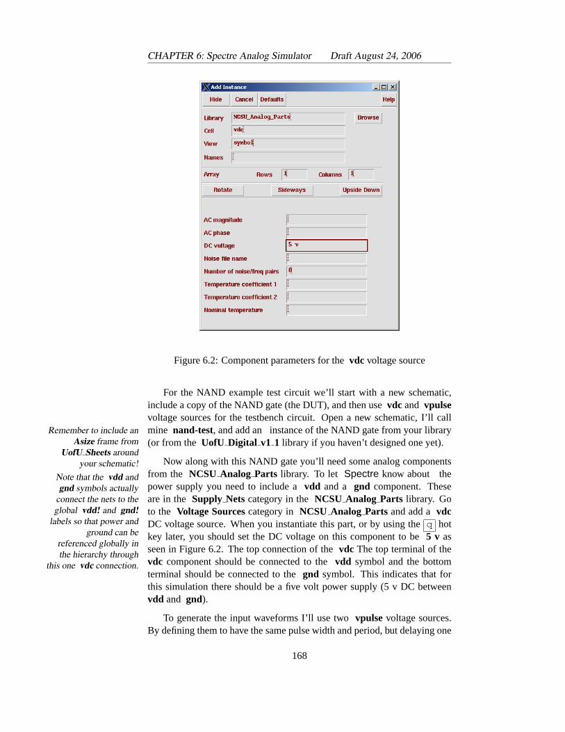
CHAPTER 6: Spectre Analog Simulator Draft August 24, 2006
Figure 6.2: Component parameters for thevdc voltage source
For the NAND example test circuit we’ll start with a new schematic,include a copy of the NAND gate (the DUT), and then usevdc and vpulsevoltage sources for the testbench circuit. Open a new schematic, I’ll callmine nand-test, and add an instance of the NAND gate from your libraryRemember to include an
Asize frame fromUofU Sheets around
your schematic!
(or from the UofU Digital v1 1 library if you haven’t designed one yet).
Now along with this NAND gate you’ll need some analog componentsfrom the NCSU Analog Parts library. To let Spectre know about theNote that the vdd and
gnd symbols actuallyconnect the nets to theglobal vdd! and gnd!
labels so that power andground can be
referenced globally inthe hierarchy through
this one vdc connection.
power supply you need to include avdd and a gnd component. Theseare in the Supply Netscategory in theNCSU Analog Parts library. Goto the Voltage Sourcescategory in NCSU Analog Parts and add avdcDC voltage source. When you instantiate this part, or by using theq hotkey later, you should set the DC voltage on this component to be5 v asseen in Figure 6.2. The top connection of thevdc The top terminal of thevdc component should be connected to thevdd symbol and the bottomterminal should be connected to thegnd symbol. This indicates that forthis simulation there should be a five volt power supply (5 v DC betweenvdd and gnd).
To generate the input waveforms I’ll use twovpulse voltage sources.By defining them to have the same pulse width and period, but delaying one
168
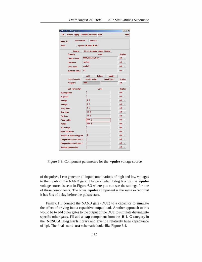
Draft August 24, 2006 6.1: Simulating a Schematic
Figure 6.3: Component parameters for thevpulsevoltage source
of the pulses, I can generate all input combinations of high and low voltagesto the inputs of the NAND gate. The parameter dialog box for thevpulsevoltage source is seen in Figure 6.3 where you can see the settings for oneof these components. The othervpulsecomponent is the same except thatit has 5ns of delay before the pulses start.
Finally, I’ll connect the NAND gate (DUT) to a capacitor to simulatethe effect of driving into a capacitive output load. Another approach to thiswould be to add other gates to the output of the DUT to simulate driving intospecific other gates. I’ll add acapcomponent from theR L C category inthe NCSU Analog Parts library and give it a relatively huge capacitanceof 1pf. The final nand-testschematic looks like Figure 6.4.
169
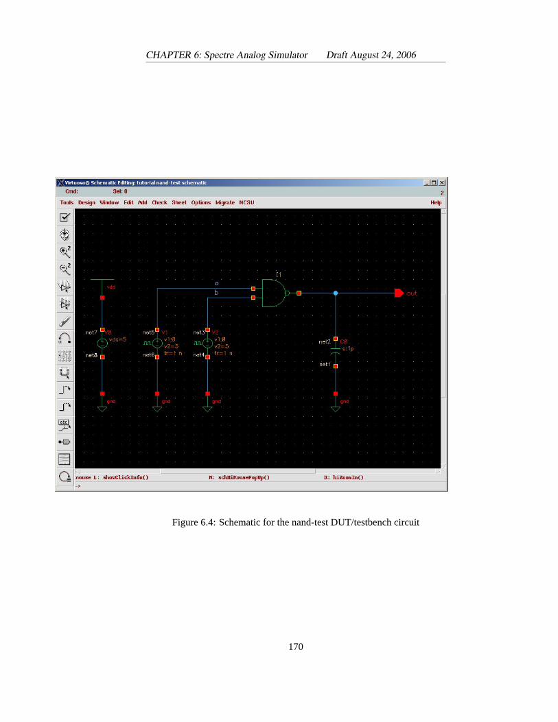
CHAPTER 6: Spectre Analog Simulator Draft August 24, 2006
Figure 6.4: Schematic for the nand-test DUT/testbench circuit
170
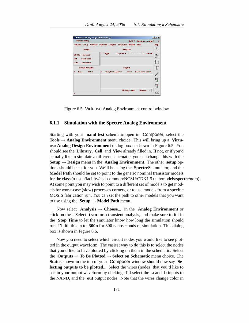
Draft August 24, 2006 6.1: Simulating a Schematic
Figure 6.5:Virtuoso Analog Environment control window
6.1.1 Simulation with the Spectre Analog Environment
Starting with your nand-test schematic open inComposer, select theTools→ Analog Environment menu choice. This will bring up aVirtu-oso Analog Design Environmentdialog box as shown in Figure 6.5. Youshould see theLibrary , Cell, and View already filled in. If not, or if you’dactually like to simulate a different schematic, you can change this with theSetup→ Designmenu in theAnalog Environment. The othersetupop-tions should be set for you. We’ll be using theSpectreSsimulator, and theModel Path should be set to point to the generic nominal transistor modelsfor the class (/uusoc/facility/cadcommon/NCSU/CDK1.5.utah/models/spectre/nom).At some point you may wish to point to a different set of models to get mod-els for worst-case (slow) processes corners, or to use models from a specificMOSIS fabrication run. You can set the path to other models that you wantto use using theSetup→ Model Path menu.
Now select Analysis → Choose... in the Analog Environment orclick on the . Selecttran for a transient analysis, and make sure to fill inthe Stop Time to let the simulator know how long the simulation shouldrun. I’ll fill this in to 300n for 300 nanoseconds of simulation. This dialogbox is shown in Figure 6.6.
Now you need to select which circuit nodes you would like to see plot-ted in the output waveform. The easiest way to do this is to select the nodesthat you’d like to have plotted by clicking on them in the schematic. Selectthe Outputs → To Be Plotted→ Select on Schematicmenu choice. TheStatusshown in the top of yourComposer window should now saySe-lecting outputs to be plotted...Select the wires (nodes) that you’d like tosee in your output waveform by clicking. I’ll select thea and b inputs tothe NAND, and theout output nodes. Note that the wires change color in
171
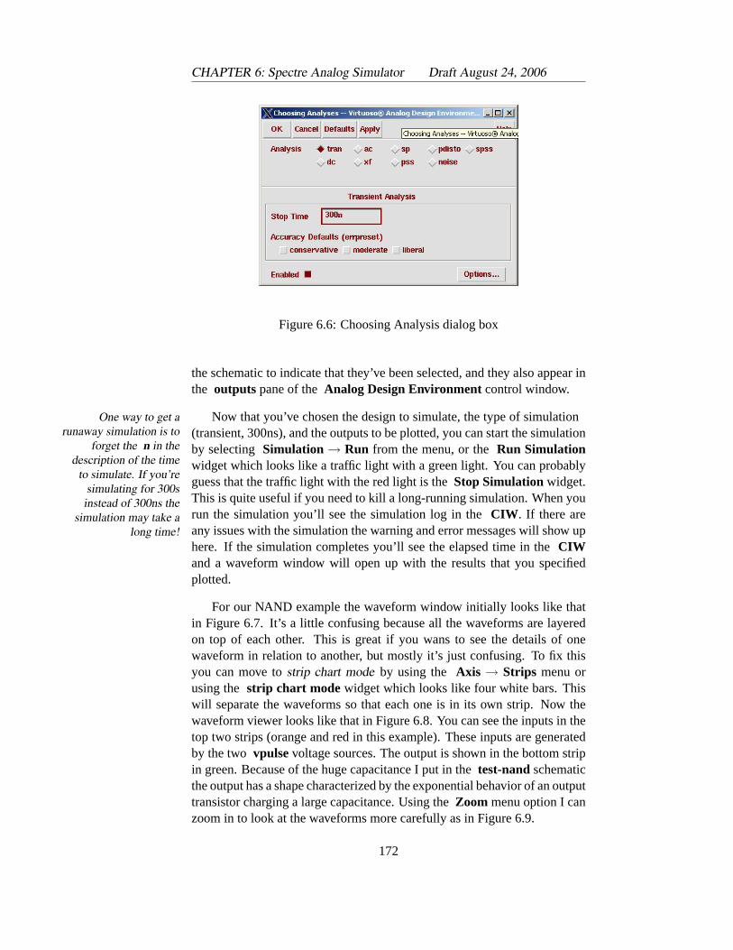
CHAPTER 6: Spectre Analog Simulator Draft August 24, 2006
Figure 6.6: Choosing Analysis dialog box
the schematic to indicate that they’ve been selected, and they also appear inthe outputs pane of theAnalog Design Environmentcontrol window.
Now that you’ve chosen the design to simulate, the type of simulationOne way to get arunaway simulation is to
forget the n in thedescription of the time
to simulate. If you’resimulating for 300sinstead of 300ns the
simulation may take along time!
(transient, 300ns), and the outputs to be plotted, you can start the simulationby selecting Simulation → Run from the menu, or theRun Simulationwidget which looks like a traffic light with a green light. You can probablyguess that the traffic light with the red light is theStop Simulationwidget.This is quite useful if you need to kill a long-running simulation. When yourun the simulation you’ll see the simulation log in theCIW . If there areany issues with the simulation the warning and error messages will show uphere. If the simulation completes you’ll see the elapsed time in theCIWand a waveform window will open up with the results that you specifiedplotted.
For our NAND example the waveform window initially looks like thatin Figure 6.7. It’s a little confusing because all the waveforms are layeredon top of each other. This is great if you wans to see the details of onewaveform in relation to another, but mostly it’s just confusing. To fix thisyou can move tostrip chart mode by using the Axis → Strips menu orusing the strip chart mode widget which looks like four white bars. Thiswill separate the waveforms so that each one is in its own strip. Now thewaveform viewer looks like that in Figure 6.8. You can see the inputs in thetop two strips (orange and red in this example). These inputs are generatedby the two vpulsevoltage sources. The output is shown in the bottom stripin green. Because of the huge capacitance I put in thetest-nandschematicthe output has a shape characterized by the exponential behavior of an outputtransistor charging a large capacitance. Using theZoom menu option I canzoom in to look at the waveforms more carefully as in Figure 6.9.
172
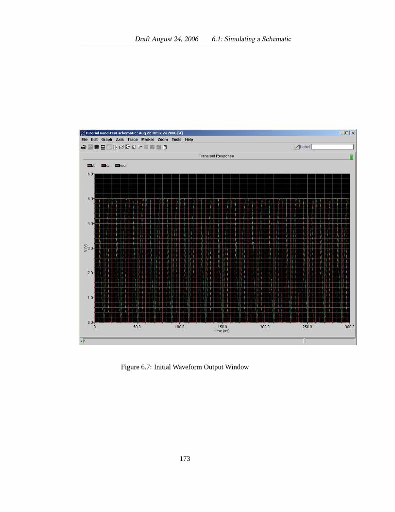
Draft August 24, 2006 6.1: Simulating a Schematic
Figure 6.7: Initial Waveform Output Window
173
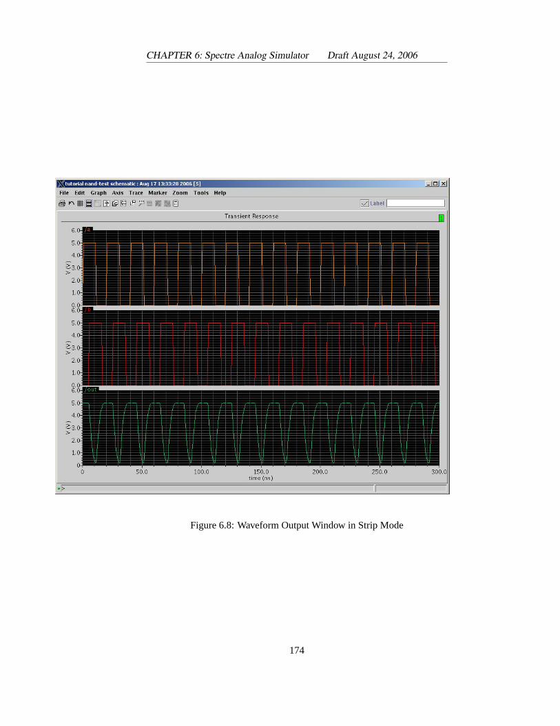
CHAPTER 6: Spectre Analog Simulator Draft August 24, 2006
Figure 6.8: Waveform Output Window in Strip Mode
174
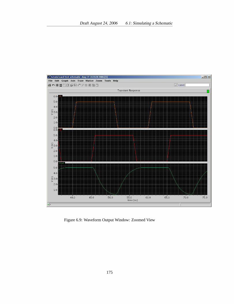
Draft August 24, 2006 6.1: Simulating a Schematic
Figure 6.9: Waveform Output Window: Zoomed View
175
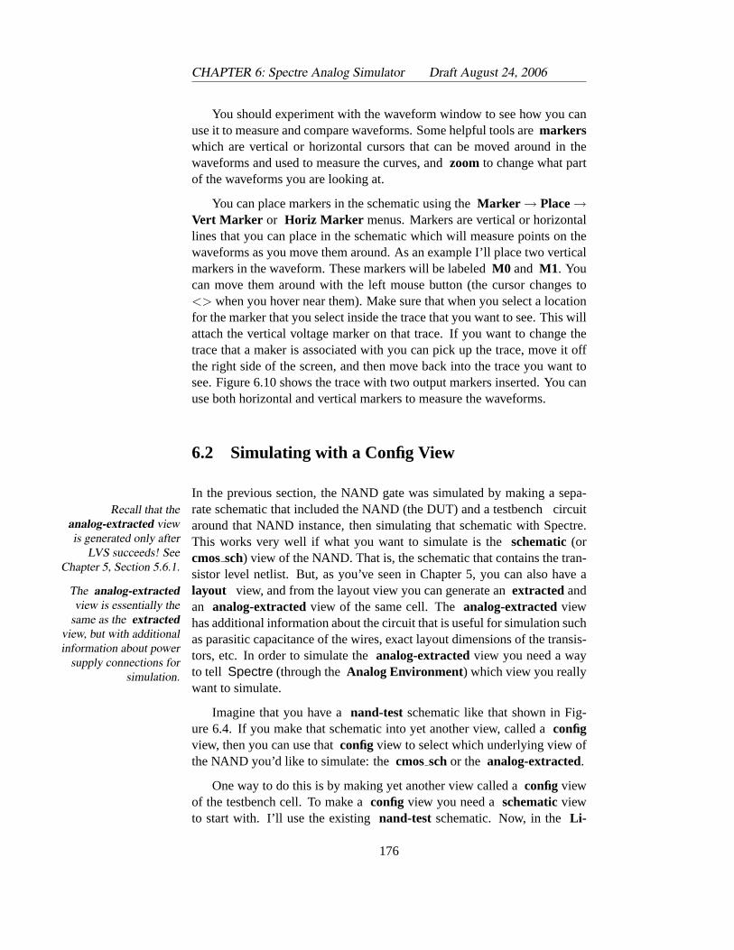
CHAPTER 6: Spectre Analog Simulator Draft August 24, 2006
You should experiment with the waveform window to see how you canuse it to measure and compare waveforms. Some helpful tools aremarkerswhich are vertical or horizontal cursors that can be moved around in thewaveforms and used to measure the curves, andzoom to change what partof the waveforms you are looking at.
You can place markers in the schematic using theMarker → Place→Vert Marker or Horiz Marker menus. Markers are vertical or horizontallines that you can place in the schematic which will measure points on thewaveforms as you move them around. As an example I’ll place two verticalmarkers in the waveform. These markers will be labeledM0 and M1. Youcan move them around with the left mouse button (the cursor changes to<> when you hover near them). Make sure that when you select a locationfor the marker that you select inside the trace that you want to see. This willattach the vertical voltage marker on that trace. If you want to change thetrace that a maker is associated with you can pick up the trace, move it offthe right side of the screen, and then move back into the trace you want tosee. Figure 6.10 shows the trace with two output markers inserted. You canuse both horizontal and vertical markers to measure the waveforms.
6.2 Simulating with a Config View
In the previous section, the NAND gate was simulated by making a sepa-rate schematic that included the NAND (the DUT) and a testbench circuitRecall that the
analog-extracted viewis generated only after
LVS succeeds! SeeChapter 5, Section 5.6.1.
around that NAND instance, then simulating that schematic with Spectre.This works very well if what you want to simulate is theschematic(orcmossch) view of the NAND. That is, the schematic that contains the tran-sistor level netlist. But, as you’ve seen in Chapter 5, you can also have alayout view, and from the layout view you can generate anextractedandThe analog-extracted
view is essentially thesame as the extracted
view, but with additionalinformation about power
supply connections forsimulation.
an analog-extractedview of the same cell. Theanalog-extractedviewhas additional information about the circuit that is useful for simulation suchas parasitic capacitance of the wires, exact layout dimensions of the transis-tors, etc. In order to simulate theanalog-extractedview you need a wayto tell Spectre (through theAnalog Environment) which view you reallywant to simulate.
Imagine that you have anand-test schematic like that shown in Fig-ure 6.4. If you make that schematic into yet another view, called aconfigview, then you can use thatconfig view to select which underlying view ofthe NAND you’d like to simulate: thecmosschor the analog-extracted.
One way to do this is by making yet another view called aconfig viewof the testbench cell. To make aconfig view you need aschematicviewto start with. I’ll use the existingnand-test schematic. Now, in theLi-
176
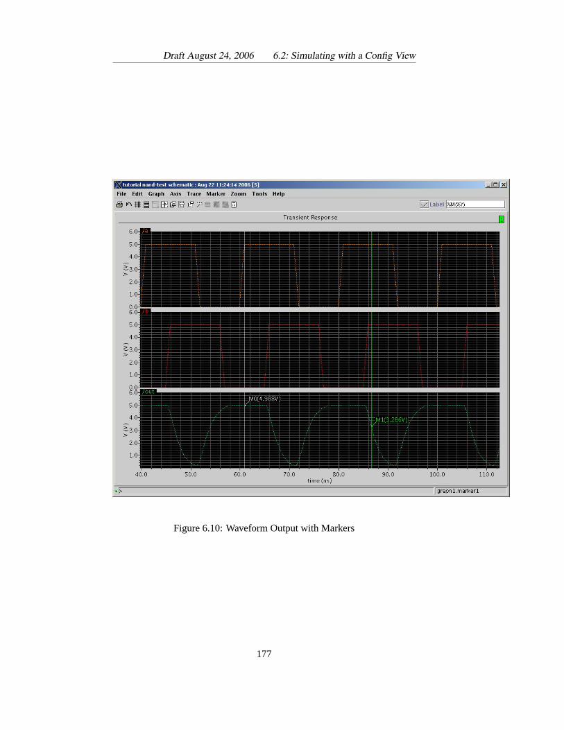
Draft August 24, 2006 6.2: Simulating with a Config View
Figure 6.10: Waveform Output with Markers
177
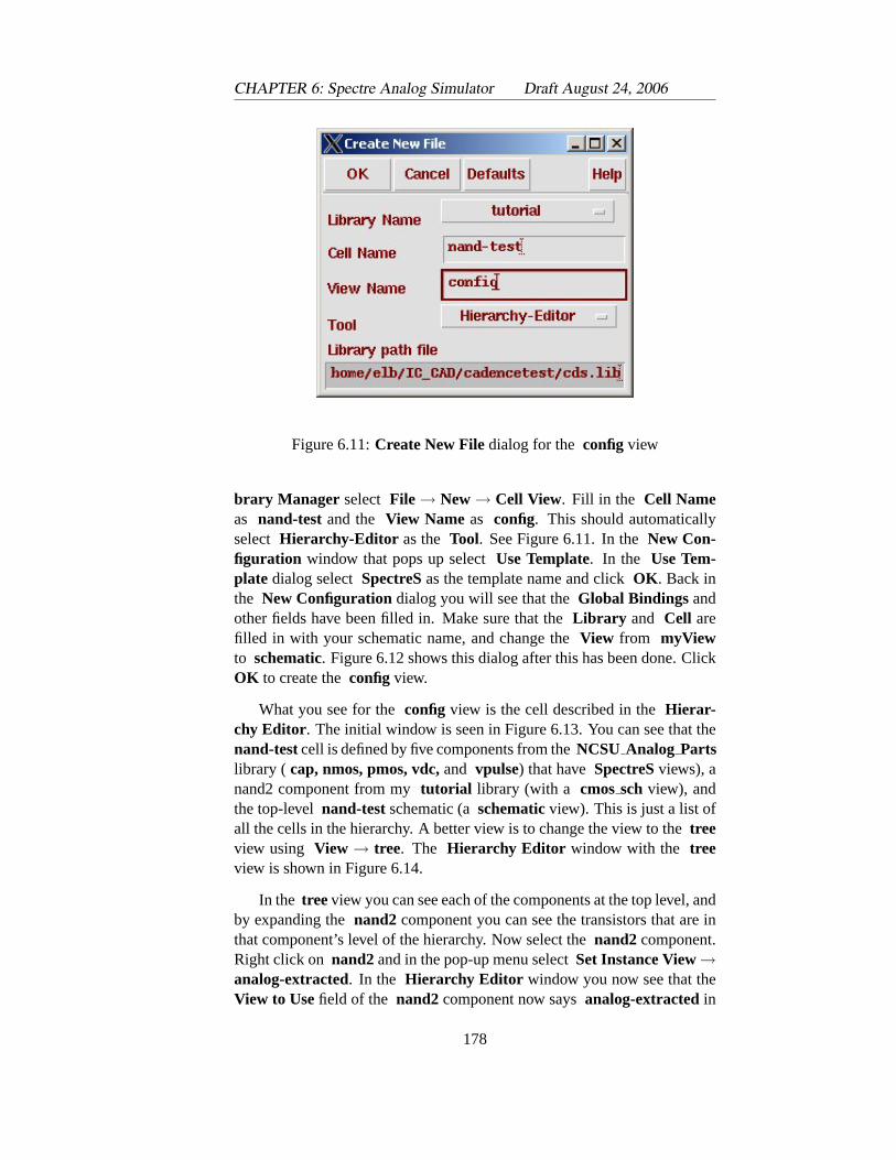
CHAPTER 6: Spectre Analog Simulator Draft August 24, 2006
Figure 6.11:Create New Filedialog for the configview
brary Manager select File → New→ Cell View. Fill in the Cell Nameas nand-test and the View Name as config. This should automaticallyselect Hierarchy-Editor as the Tool. See Figure 6.11. In theNew Con-figuration window that pops up selectUse Template. In the Use Tem-plate dialog selectSpectreSas the template name and clickOK . Back inthe New Configuration dialog you will see that theGlobal Bindings andother fields have been filled in. Make sure that theLibrary and Cell arefilled in with your schematic name, and change theView from myViewto schematic. Figure 6.12 shows this dialog after this has been done. ClickOK to create theconfigview.
What you see for theconfig view is the cell described in theHierar-chy Editor . The initial window is seen in Figure 6.13. You can see that thenand-testcell is defined by five components from theNCSU Analog Partslibrary ( cap, nmos, pmos, vdc,and vpulse) that haveSpectreSviews), anand2 component from mytutorial library (with a cmossch view), andthe top-levelnand-testschematic (aschematicview). This is just a list ofall the cells in the hierarchy. A better view is to change the view to thetreeview using View → tree. The Hierarchy Editor window with the treeview is shown in Figure 6.14.
In the tree view you can see each of the components at the top level, andby expanding thenand2 component you can see the transistors that are inthat component’s level of the hierarchy. Now select thenand2 component.Right click on nand2and in the pop-up menu selectSet Instance View→analog-extracted. In the Hierarchy Editor window you now see that theView to Usefield of the nand2 component now saysanalog-extractedin
178
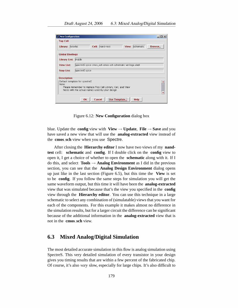
Draft August 24, 2006 6.3: Mixed Analog/Digital Simulation
Figure 6.12:New Configuration dialog box
blue. Update theconfigview with View→ Update, File→ Saveand youhave saved a new view that will use theanalog-extractedview instead ofthe cmosschview when you useSpectre.
After closing theHierarchy editor I now have two views of mynand-test cell: schematicand config. If I double click on the config view toopen it, I get a choice of whether to open theschematicalong with it. If Ido this, and selectTools→ Analog Environment as I did in the previoussection, you can see that theAnalog Design Environmentdialog opensup just like in the last section (Figure 6.5), but this time theView is setto be config. If you follow the same steps for simulation you will get thesame waveform output, but this time it will have been theanalog-extractedview that was simulated because that’s the view you specified in theconfigview through theHierarchy editor . You can use this technique in a largeschematic to select any combination of (simulatable) views that you want foreach of the components. For this example it makes almost no difference inthe simulation results, but for a larger circuit the difference can be significantbecause of the additional information in theanalog-extractedview that isnot in the cmosschview.
6.3 Mixed Analog/Digital Simulation
The most detailed accurate simulation in this flow is analog simulation usingSpectreS. This very detailed simulation of every transistor in your designgives you timing results that are within a few percent of the fabricated chip.Of course, it’s alsovery slow, especially for large chips. It’s also difficult to
179
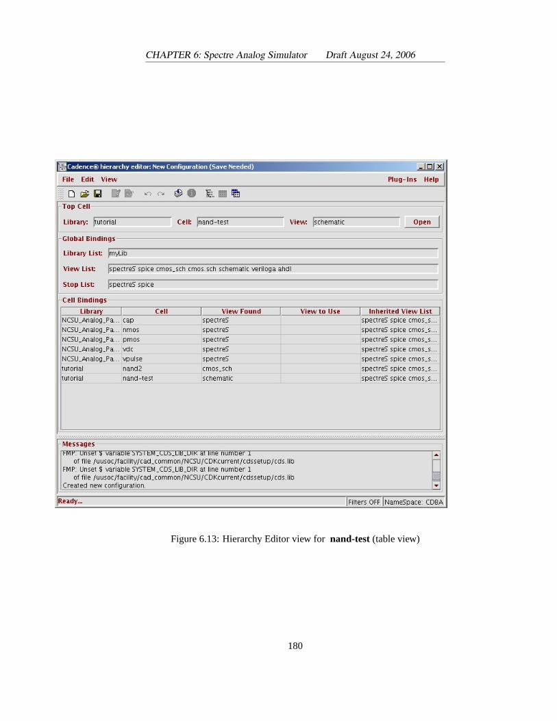
CHAPTER 6: Spectre Analog Simulator Draft August 24, 2006
Figure 6.13: Hierarchy Editor view fornand-test(table view)
180
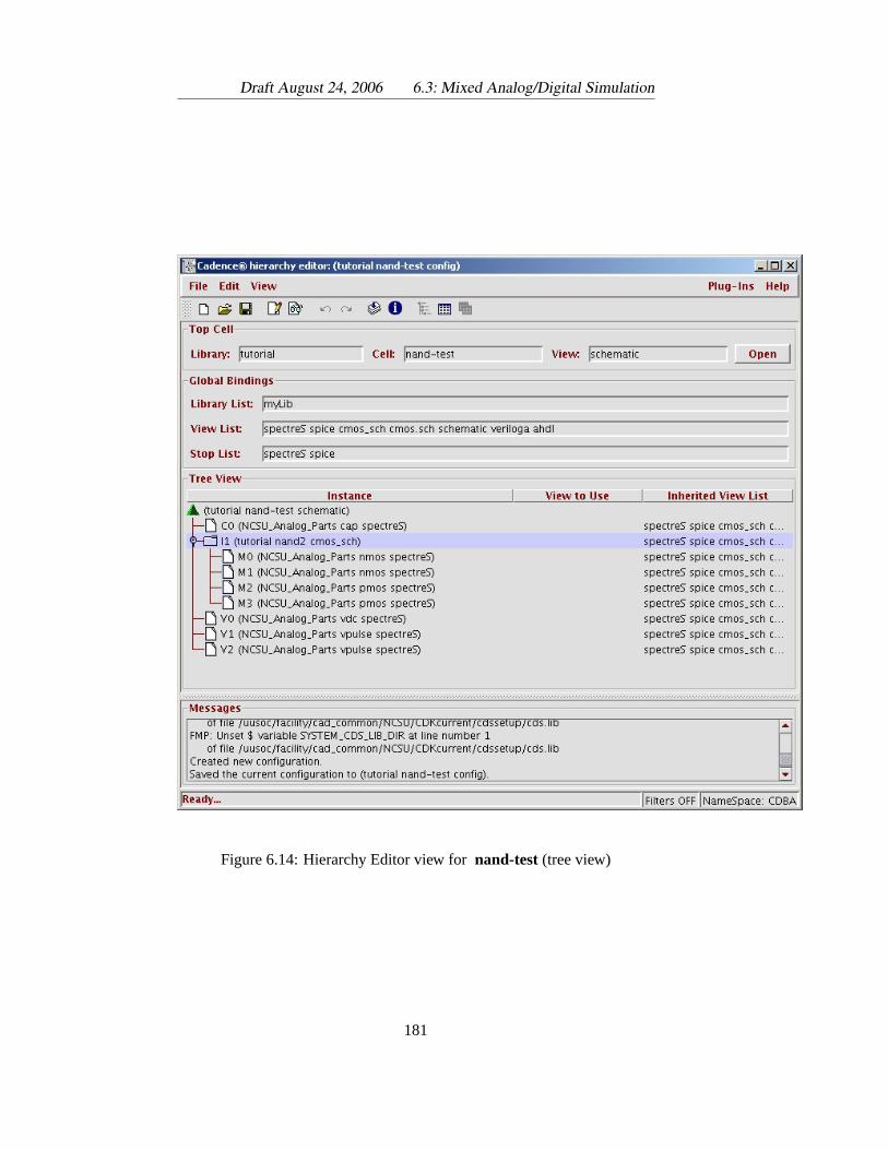
Draft August 24, 2006 6.3: Mixed Analog/Digital Simulation
Figure 6.14: Hierarchy Editor view fornand-test(tree view)
181
CHAPTER 6: Spectre Analog Simulator Draft August 24, 2006
use thevpulseand vpwl components to generate complex data streams fordigital circuits. However, if you really want good timing information aboutEven more detailed
simulation is possiblethat includes 3-d
transistor andinterconnect models,
fild-solvers forundertanding the effects
of changing signals,localized heating, and
many other effects, butthey’re beyond the scope
of this flow.
your chip, there’s no substitute for analog simulation of the whole chip!
Luckily, there is a compromise between full analog simulation and purelyfunctional simulation.Cadence is designed to do mixed mode simulationwhere part of your design is simulated usingVerilog-XL or NC Verilogand part is simulated usingSpectreS. You can use this capability for avariety of simulation tasks.
1. You can simulate circuits that are actually mixed mode circuits. Thatis, systems that have both analog and digital components like a suc-cessive approximation ADC.
2. You can simulate large digital systems by simulating most of the cir-cuit using a Verilog simulator, but specify that certain critical partsare simulated using the analog simulator for more accuracy.
3. You can simulate the entire system with the analog simulator, but havea small set of digital components in your testbench file so that youcan write the testbench in Verilog instead of usingvpulseand vpwlcomponents.
Cadence does through theconfig view that was described in the pre-vious section. It also automatically installsinterface elements between thedigital and analog portions of the design (they’re calleda2dand d2a), andautomatically interfaces the two simulators.
To set up for mixed mode simulation you need a top-level schematic thatincludes your DUT, and also components that drive the input and deliver theoutputs. In the top-level schematic for the pureSpectre case the inputswere driven by analog voltage sources. Because we want to drive the inputsfrom Verilog in this case, the inputs should be driven by digital sources.Because the mixed-mode simulator wants to include interface elements be-tween the digital and analog parts of the circuit, I’m going to include twoinverters in a row driving the inputs, and two inverters in a row for the out-put signals. This will let me make one of thse inverters digital (so that itcan be driven from Verilog) and the second inverter can be analog (so that itwill provide an analog signal to the NAND gate DUT). If there are inputs toyour DUT that you want to be driven from analog voltage sources you canalso include those in this test schematic. Because part of the simulation isanalog, you also need to include thevdc for the power supply connectionin any case. Themixed-testschematic is shown in Figure 6.15.
Create a config view of your testbench schematic as if you were doingan analog simulation. When you get to theNew Configuration dialog box,
182
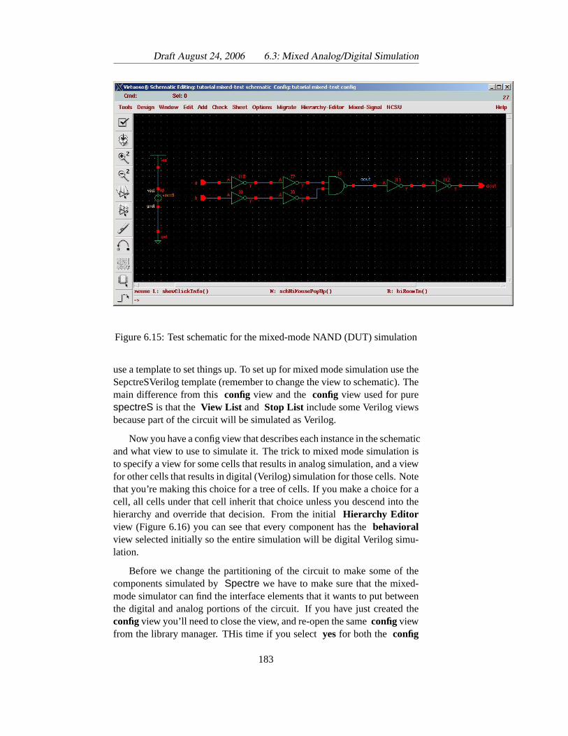
Draft August 24, 2006 6.3: Mixed Analog/Digital Simulation
Figure 6.15: Test schematic for the mixed-mode NAND (DUT) simulation
use a template to set things up. To set up for mixed mode simulation use theSepctreSVerilog template (remember to change the view to schematic). Themain difference from thisconfig view and the config view used for purespectreS is that theView List and Stop List include some Verilog viewsbecause part of the circuit will be simulated as Verilog.
Now you have a config view that describes each instance in the schematicand what view to use to simulate it. The trick to mixed mode simulation isto specify a view for some cells that results in analog simulation, and a viewfor other cells that results in digital (Verilog) simulation for those cells. Notethat you’re making this choice for a tree of cells. If you make a choice for acell, all cells under that cell inherit that choice unless you descend into thehierarchy and override that decision. From the initialHierarchy Editorview (Figure 6.16) you can see that every component has thebehavioralview selected initially so the entire simulation will be digital Verilog simu-lation.
Before we change the partitioning of the circuit to make some of thecomponents simulated bySpectre we have to make sure that the mixed-mode simulator can find the interface elements that it wants to put betweenthe digital and analog portions of the circuit. If you have just created theconfigview you’ll need to close the view, and re-open the sameconfigviewfrom the library manager. THis time if you selectyesfor both the config
183
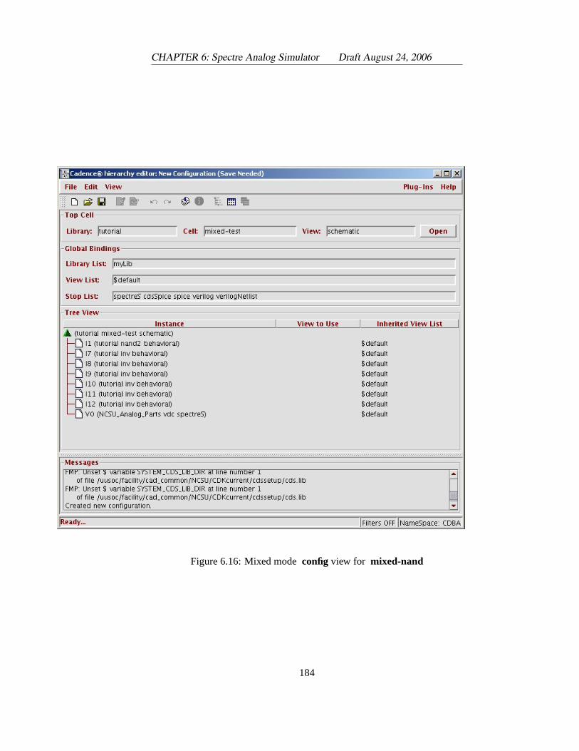
CHAPTER 6: Spectre Analog Simulator Draft August 24, 2006
Figure 6.16: Mixed modeconfigview for mixed-nand
184
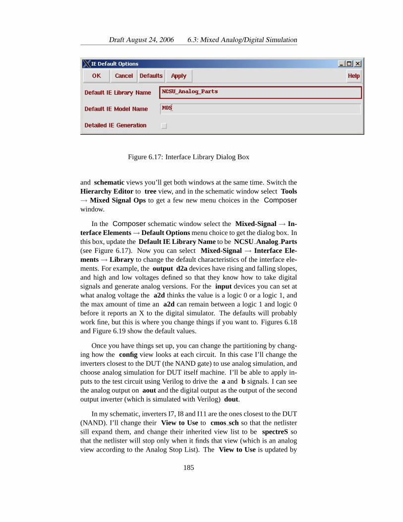
Draft August 24, 2006 6.3: Mixed Analog/Digital Simulation
Figure 6.17: Interface Library Dialog Box
and schematicviews you’ll get both windows at the same time. Switch theHierarchy Editor to tree view, and in the schematic window selectTools→ Mixed Signal Ops to get a few new menu choices in theComposerwindow.
In the Composer schematic window select theMixed-Signal→ In-terface Elements→Default Options menu choice to get the dialog box. Inthis box, update theDefault IE Library Name to be NCSU Analog Parts(see Figure 6.17). Now you can selectMixed-Signal → Interface Ele-ments→ Library to change the default characteristics of the interface ele-ments. For example, theoutput d2a devices have rising and falling slopes,and high and low voltages defined so that they know how to take digitalsignals and generate analog versions. For theinput devices you can set atwhat analog voltage thea2d thinks the value is a logic 0 or a logic 1, andthe max amount of time ana2d can remain between a logic 1 and logic 0before it reports an X to the digital simulator. The defaults will probablywork fine, but this is where you change things if you want to. Figures 6.18and Figure 6.19 show the default values.
Once you have things set up, you can change the partitioning by chang-ing how the config view looks at each circuit. In this case I’ll change theinverters closest to the DUT (the NAND gate) to use analog simulation, andchoose analog simulation for DUT itself machine. I’ll be able to apply in-puts to the test circuit using Verilog to drive thea and b signals. I can seethe analog output onaout and the digital output as the output of the secondoutput inverter (which is simulated with Verilog)dout.
In my schematic, inverters I7, I8 and I11 are the ones closest to the DUT(NAND). I’ll change their View to Use to cmossch so that the netlistersill expand them, and change their inherited view list to bespectreSsothat the netlister will stop only when it finds that view (which is an analogview according to the Analog Stop List). TheView to Use is updated by
185
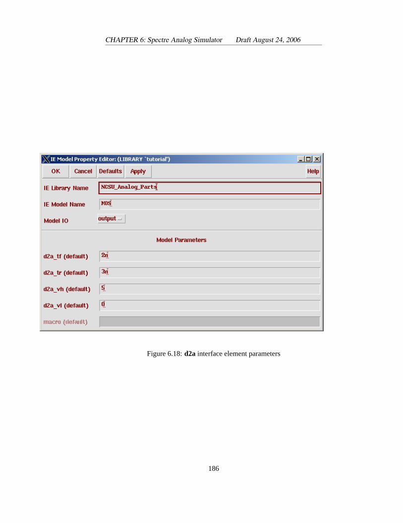
CHAPTER 6: Spectre Analog Simulator Draft August 24, 2006
Figure 6.18:d2a interface element parameters
186
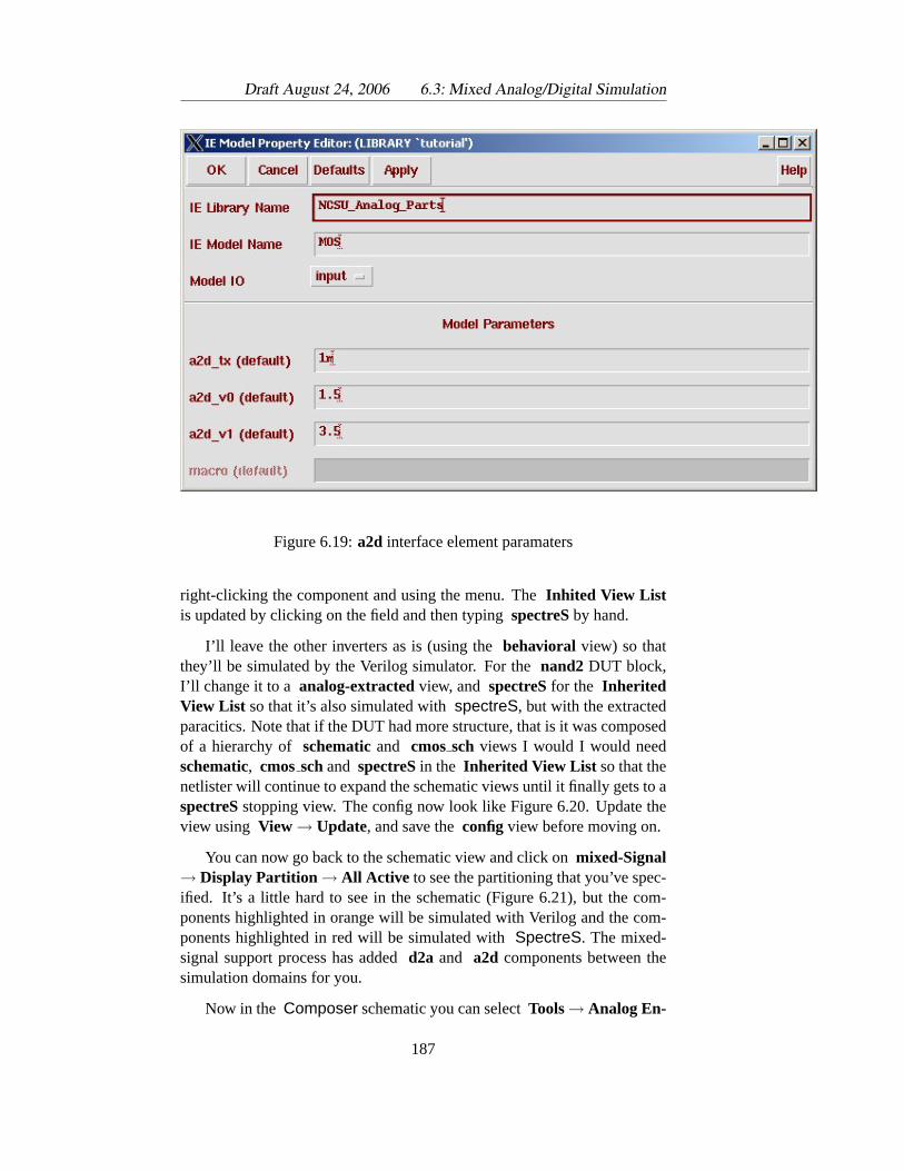
Draft August 24, 2006 6.3: Mixed Analog/Digital Simulation
Figure 6.19:a2d interface element paramaters
right-clicking the component and using the menu. TheInhited View Listis updated by clicking on the field and then typingspectreSby hand.
I’ll leave the other inverters as is (using thebehavioral view) so thatthey’ll be simulated by the Verilog simulator. For thenand2 DUT block,I’ll change it to a analog-extractedview, and spectreSfor the InheritedView List so that it’s also simulated withspectreS, but with the extractedparacitics. Note that if the DUT had more structure, that is it was composedof a hierarchy of schematicand cmossch views I would I would needschematic, cmosschand spectreSin the Inherited View List so that thenetlister will continue to expand the schematic views until it finally gets to aspectreSstopping view. The config now look like Figure 6.20. Update theview using View → Update, and save theconfigview before moving on.
You can now go back to the schematic view and click onmixed-Signal→ Display Partition → All Active to see the partitioning that you’ve spec-ified. It’s a little hard to see in the schematic (Figure 6.21), but the com-ponents highlighted in orange will be simulated with Verilog and the com-ponents highlighted in red will be simulated withSpectreS. The mixed-signal support process has addedd2a and a2d components between thesimulation domains for you.
Now in the Composer schematic you can selectTools→ Analog En-
187
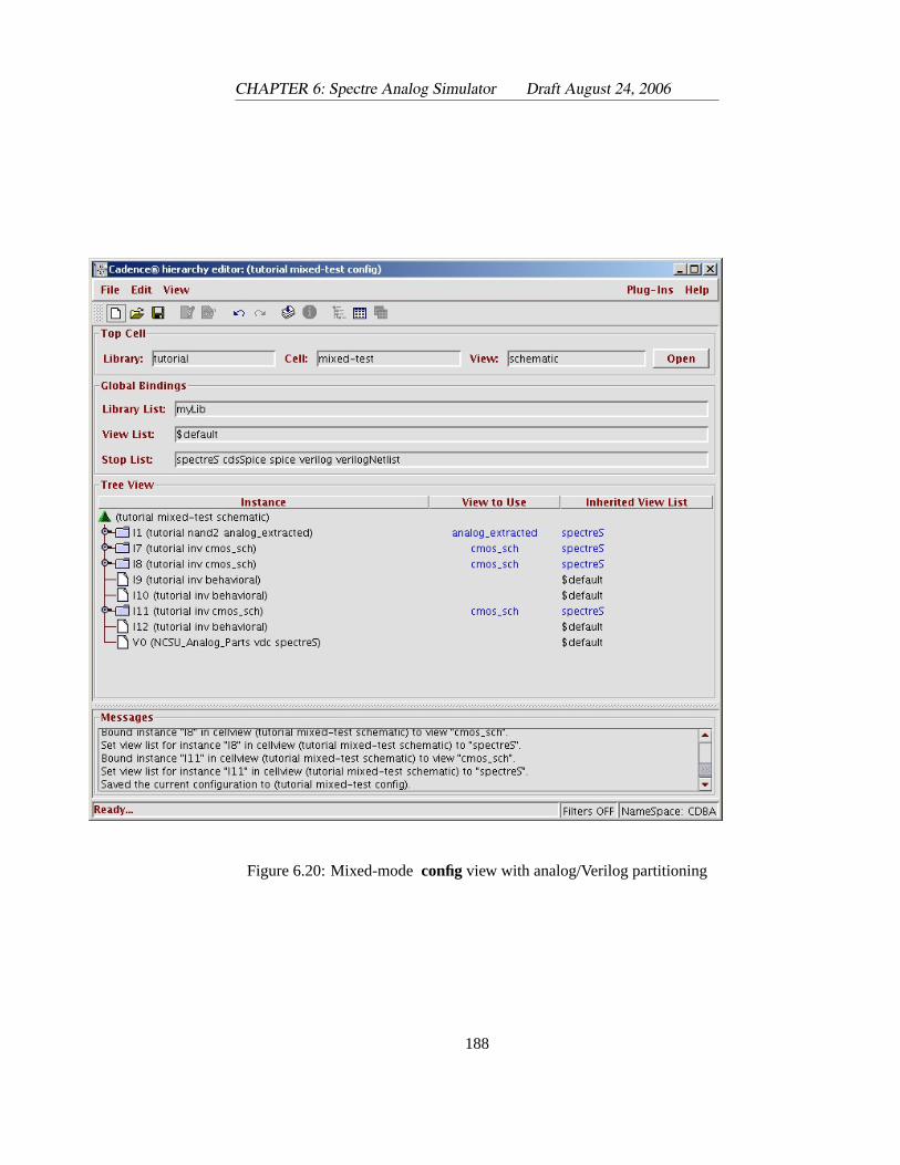
CHAPTER 6: Spectre Analog Simulator Draft August 24, 2006
Figure 6.20: Mixed-modeconfigview with analog/Verilog partitioning
188
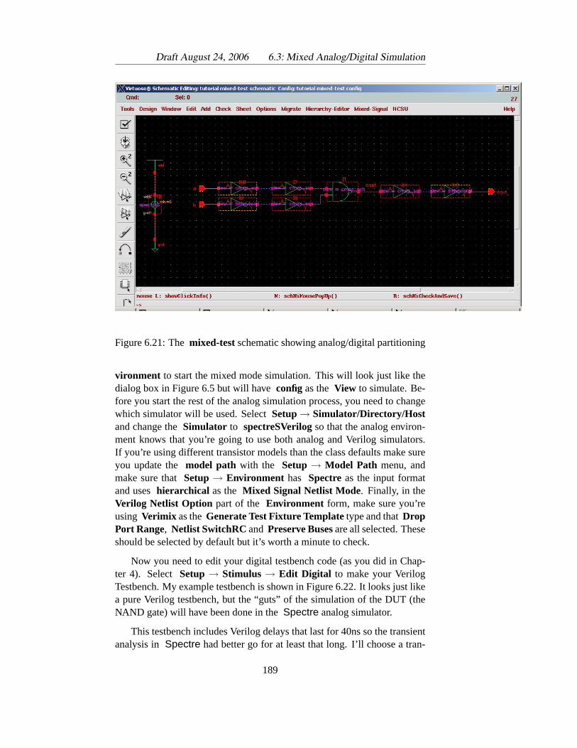
Draft August 24, 2006 6.3: Mixed Analog/Digital Simulation
Figure 6.21: Themixed-testschematic showing analog/digital partitioning
vironment to start the mixed mode simulation. This will look just like thedialog box in Figure 6.5 but will haveconfig as theView to simulate. Be-fore you start the rest of the analog simulation process, you need to changewhich simulator will be used. SelectSetup→ Simulator/Directory/Hostand change theSimulator to spectreSVerilogso that the analog environ-ment knows that you’re going to use both analog and Verilog simulators.If you’re using different transistor models than the class defaults make sureyou update themodel path with the Setup→ Model Path menu, andmake sure thatSetup→ Environment has Spectreas the input formatand useshierarchical as the Mixed Signal Netlist Mode. Finally, in theVerilog Netlist Option part of the Environment form, make sure you’reusing Verimix as theGenerate Test Fixture Templatetype and thatDropPort Range, Netlist SwitchRC and Preserve Busesare all selected. Theseshould be selected by default but it’s worth a minute to check.
Now you need to edit your digital testbench code (as you did in Chap-ter 4). Select Setup→ Stimulus → Edit Digital to make your VerilogTestbench. My example testbench is shown in Figure 6.22. It looks just likea pure Verilog testbench, but the “guts” of the simulation of the DUT (theNAND gate) will have been done in theSpectre analog simulator.
This testbench includes Verilog delays that last for 40ns so the transientanalysis in Spectre had better go for at least that long. I’ll choose a tran-
189
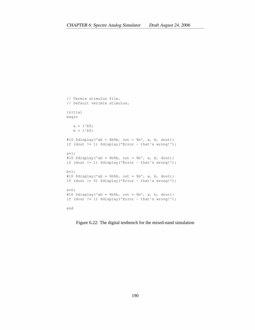
CHAPTER 6: Spectre Analog Simulator Draft August 24, 2006
// Vermix stimulus file.// Default verimix stimulus.
initialbegin
a = 1’b0;b = 1’b0;
#10 $display("ab = %b%b, out = %b", a, b, dout);if (dout != 1) $display("Error - that’s wrong!");
a=1;#10 $display("ab = %b%b, out = %b", a, b, dout);if (dout != 1) $display("Error - that’s wrong!");
b=1;#10 $display("ab = %b%b, out = %b", a, b, dout);if (dout != 0) $display("Error - that’s wrong!");
a=0;#10 $display("ab = %b%b, out = %b", a, b, dout);if (dout != 1) $display("Error - that’s wrong!");
end
Figure 6.22: The digital testbench for the mixed-nand simulation
190
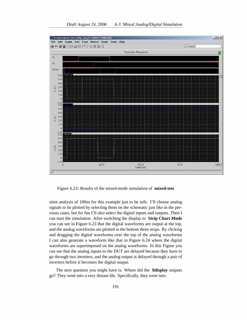
Draft August 24, 2006 6.3: Mixed Analog/Digital Simulation
Figure 6.23: Results of the mixed-mode simulation ofmixed-test
sient analysis of 100ns for this example just to be safe. I’ll choose analogsignals to be plotted by selecting them on the schematic just like in the pre-vious cases, but for fun I’ll also select the digital inputs and outputs. Then Ican start the simulation. After switching the display toStrip Chart Modeyou can see in Figure 6.23 that the digital waveforms are output at the top,and the analog waveforms are plotted in the bottom three strips. By clickingand dragging the digital waveforms over the top of the analog waveformsI can also generate a waveform like that in Figure 6.24 where the digitalwaveforms are superimposed on the analog waveforms. In this Figure youcan see that the analog inputs to the DUT are delayed because they have togo through two inverters, and the analog output is delayed through a pair ofinverters before it becomes the digital output.
The next question you might have is: Where did the$display outputsgo? They went into a very distant file. Specifically, they went into:
191
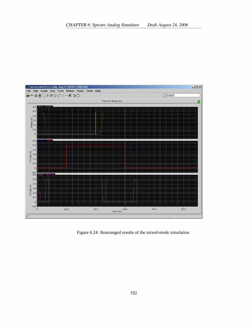
CHAPTER 6: Spectre Analog Simulator Draft August 24, 2006
Figure 6.24: Rearranged results of the mixed-mode simulation
192
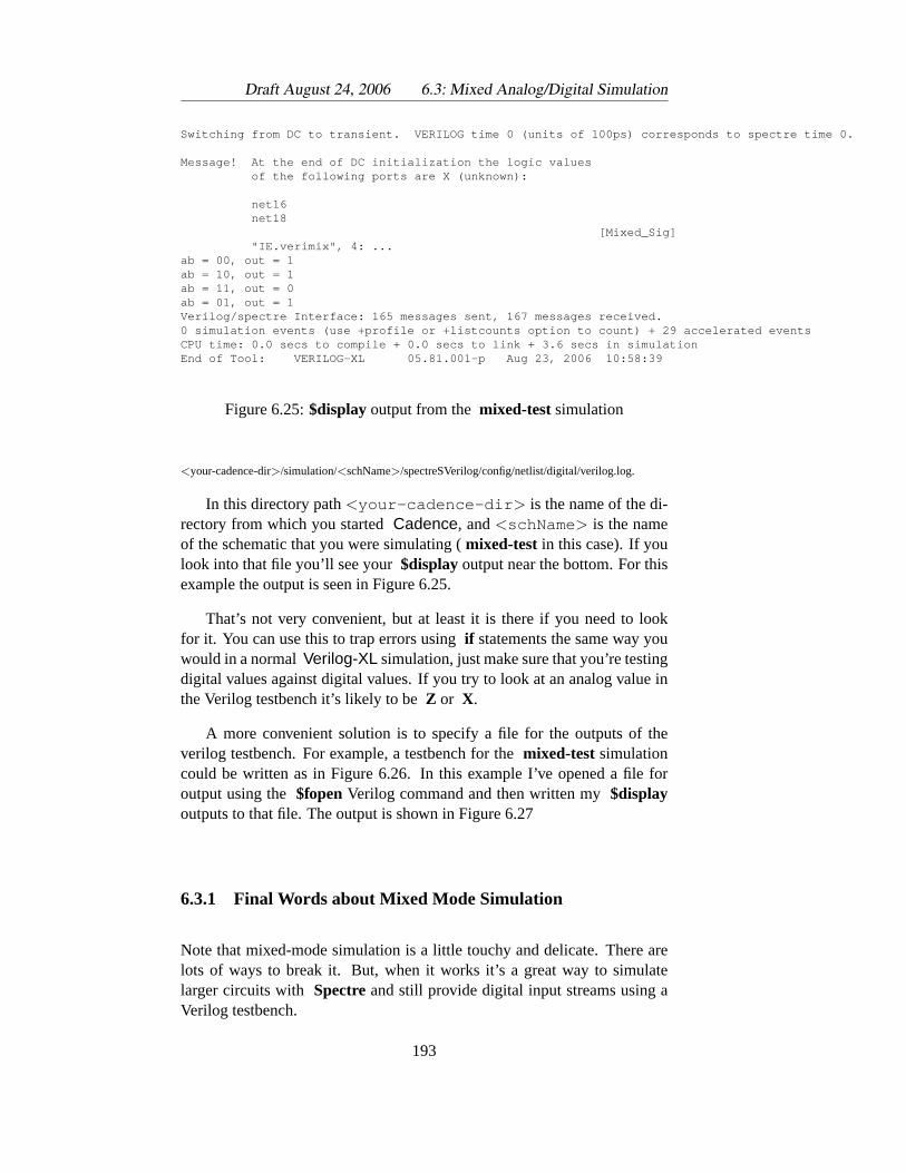
Draft August 24, 2006 6.3: Mixed Analog/Digital Simulation
Switching from DC to transient. VERILOG time 0 (units of 100ps) corresponds to spectre time 0.
Message! At the end of DC initialization the logic valuesof the following ports are X (unknown):
net16net18
[Mixed_Sig]"IE.verimix", 4: ...
ab = 00, out = 1ab = 10, out = 1ab = 11, out = 0ab = 01, out = 1Verilog/spectre Interface: 165 messages sent, 167 messages received.0 simulation events (use +profile or +listcounts option to count) + 29 accelerated eventsCPU time: 0.0 secs to compile + 0.0 secs to link + 3.6 secs in simulationEnd of Tool: VERILOG-XL 05.81.001-p Aug 23, 2006 10:58:39
Figure 6.25:$displayoutput from themixed-testsimulation
<your-cadence-dir>/simulation/<schName>/spectreSVerilog/config/netlist/digital/verilog.log.
In this directory path<your-cadence-dir > is the name of the di-rectory from which you startedCadence, and<schName> is the nameof the schematic that you were simulating (mixed-test in this case). If youlook into that file you’ll see your$display output near the bottom. For thisexample the output is seen in Figure 6.25.
That’s not very convenient, but at least it is there if you need to lookfor it. You can use this to trap errors usingif statements the same way youwould in a normalVerilog-XL simulation, just make sure that you’re testingdigital values against digital values. If you try to look at an analog value inthe Verilog testbench it’s likely to beZ or X.
A more convenient solution is to specify a file for the outputs of theverilog testbench. For example, a testbench for themixed-testsimulationcould be written as in Figure 6.26. In this example I’ve opened a file foroutput using the$fopenVerilog command and then written my$displayoutputs to that file. The output is shown in Figure 6.27
6.3.1 Final Words about Mixed Mode Simulation
Note that mixed-mode simulation is a little touchy and delicate. There arelots of ways to break it. But, when it works it’s a great way to simulatelarger circuits with Spectreand still provide digital input streams using aVerilog testbench.
193
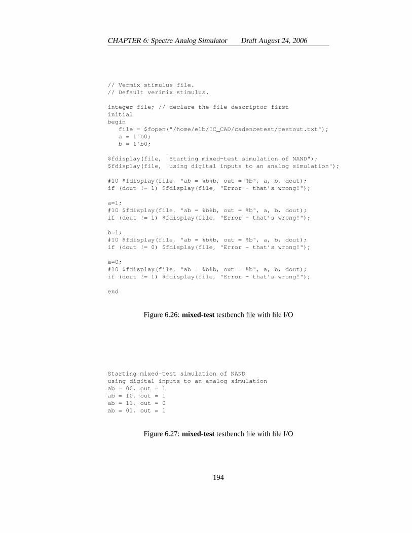
CHAPTER 6: Spectre Analog Simulator Draft August 24, 2006
// Vermix stimulus file.// Default verimix stimulus.
integer file; // declare the file descriptor firstinitialbegin
file = $fopen("/home/elb/IC_CAD/cadencetest/testout.txt");a = 1’b0;b = 1’b0;
$fdisplay(file, "Starting mixed-test simulation of NAND");$fdisplay(file, "using digital inputs to an analog simulation");
#10 $fdisplay(file, "ab = %b%b, out = %b", a, b, dout);if (dout != 1) $fdisplay(file, "Error - that’s wrong!");
a=1;#10 $fdisplay(file, "ab = %b%b, out = %b", a, b, dout);if (dout != 1) $fdisplay(file, "Error - that’s wrong!");
b=1;#10 $fdisplay(file, "ab = %b%b, out = %b", a, b, dout);if (dout != 0) $fdisplay(file, "Error - that’s wrong!");
a=0;#10 $fdisplay(file, "ab = %b%b, out = %b", a, b, dout);if (dout != 1) $fdisplay(file, "Error - that’s wrong!");
end
Figure 6.26:mixed-testtestbench file with file I/O
Starting mixed-test simulation of NANDusing digital inputs to an analog simulationab = 00, out = 1ab = 10, out = 1ab = 11, out = 0ab = 01, out = 1
Figure 6.27:mixed-testtestbench file with file I/O
194
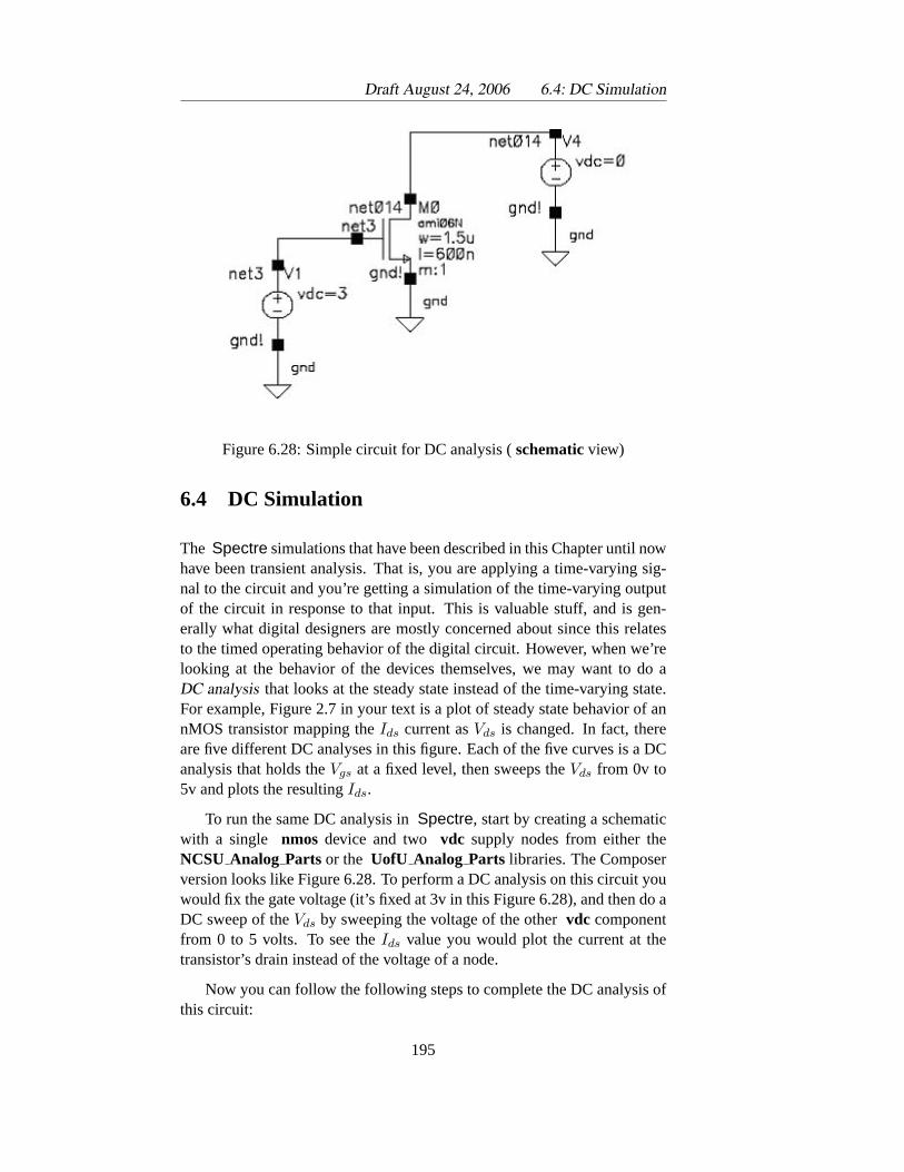
Draft August 24, 2006 6.4: DC Simulation
Figure 6.28: Simple circuit for DC analysis (schematicview)
6.4 DC Simulation
The Spectre simulations that have been described in this Chapter until nowhave been transient analysis. That is, you are applying a time-varying sig-nal to the circuit and you’re getting a simulation of the time-varying outputof the circuit in response to that input. This is valuable stuff, and is gen-erally what digital designers are mostly concerned about since this relatesto the timed operating behavior of the digital circuit. However, when we’relooking at the behavior of the devices themselves, we may want to do aDC analysis that looks at the steady state instead of the time-varying state.For example, Figure 2.7 in your text is a plot of steady state behavior of annMOS transistor mapping theIds current asVds is changed. In fact, thereare five different DC analyses in this figure. Each of the five curves is a DCanalysis that holds theVgs at a fixed level, then sweeps theVds from 0v to5v and plots the resultingIds.
To run the same DC analysis inSpectre, start by creating a schematicwith a single nmos device and two vdc supply nodes from either theNCSU Analog Parts or the UofU Analog Parts libraries. The Composerversion looks like Figure 6.28. To perform a DC analysis on this circuit youwould fix the gate voltage (it’s fixed at 3v in this Figure 6.28), and then do aDC sweep of theVds by sweeping the voltage of the othervdc componentfrom 0 to 5 volts. To see theIds value you would plot the current at thetransistor’s drain instead of the voltage of a node.
Now you can follow the following steps to complete the DC analysis ofthis circuit:
195

CHAPTER 6: Spectre Analog Simulator Draft August 24, 2006
1. Open the schematic inComposer. Set the voltages of thevdc com-ponents as they are in Figure 6.28.
2. Select Tools→ Analog Environment. When you choose thenal-ysis typeselect DC instead of tran . This changes theChoosingAnalysisdialog box to DC.
3. Choose your sweep variable for the DC analysis. In this case we’regoing to sweep the voltage of thevdc component that’s connected tothe nmos drain so chooseComponent Parameterso that we canselect the component that we want to use for the sweep.
4. This changes the dialog box so that you can tell it which componentyou’re going to select, which parameter of the component you want tovary, and what the sweep range is of that parameter. Click onSelectComponentso that you can select thevdc connected to the transistordrain by clicking on it in the schematic.
5. When you select (click on) thevdc connected to the transistor drain,you get another box (Figure 6.29)that asks you to select the compo-nent parameter that you want to sweep. We want to sweep thedcvoltage. Click on that and then OK. You’ll see that the componentname (/V1 in my circuit) and the parameter name (dc) have beenadded to theChoosing Analysisdialog box which now looks likethat in Figure 6.30.
6. Now enter the Sweep Range. Start from 0 and stop at 5. This will setup the DC analysis to sweepVds from 0v to 5v during the analysis.Click OK.
7. Back in the Analog Environment you need to select the outputs tobe plotted. Use the sameSelect on Schematicchoice that you’veused before, but instead of selecting a wire, select the red square onthe drain of thenmos transistor (the top leg of transistor M0 in Fig-ure 6.28 - the one without the arrow). This will cause a circle to be putaround the drain, and the drain current will be plotted. This shows upas M0/D for the output in my circuit (M0 is the transistor identifier,and D is the drain current). TheAnalog Environment dialog boxshould look like Figure 6.31 when you’re done.
8. Now run the simulation. You should get a waveform output like Fig-ure 6.32 that has a singleIds curve for a 3v gate voltage (Vgs) and aDC sweep from 0v to 5v onVds.
196
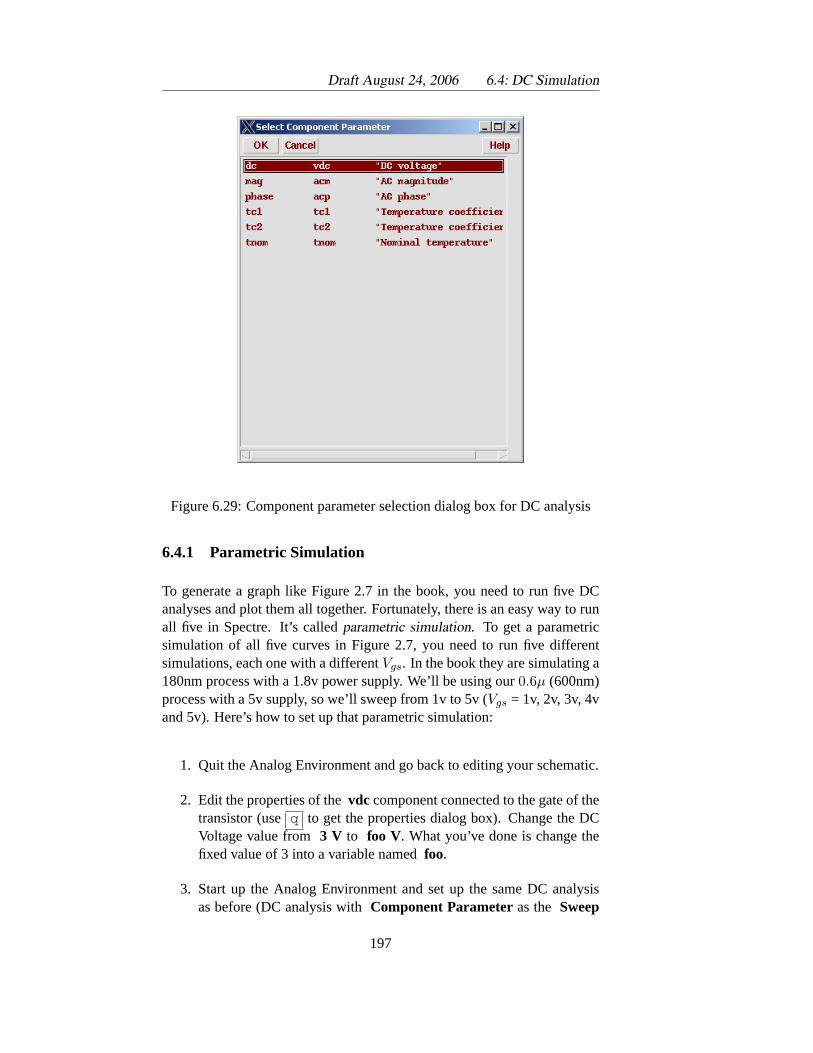
Draft August 24, 2006 6.4: DC Simulation
Figure 6.29: Component parameter selection dialog box for DC analysis
6.4.1 Parametric Simulation
To generate a graph like Figure 2.7 in the book, you need to run five DCanalyses and plot them all together. Fortunately, there is an easy way to runall five in Spectre. It’s calledparametric simulation. To get a parametricsimulation of all five curves in Figure 2.7, you need to run five differentsimulations, each one with a differentVgs. In the book they are simulating a180nm process with a 1.8v power supply. We’ll be using our0.6µ (600nm)process with a 5v supply, so we’ll sweep from 1v to 5v (Vgs = 1v, 2v, 3v, 4vand 5v). Here’s how to set up that parametric simulation:
1. Quit the Analog Environment and go back to editing your schematic.
2. Edit the properties of thevdc component connected to the gate of thetransistor (useq to get the properties dialog box). Change the DCVoltage value from3 V to foo V. What you’ve done is change thefixed value of 3 into a variable namedfoo.
3. Start up the Analog Environment and set up the same DC analysisas before (DC analysis withComponent Parameteras the Sweep
197
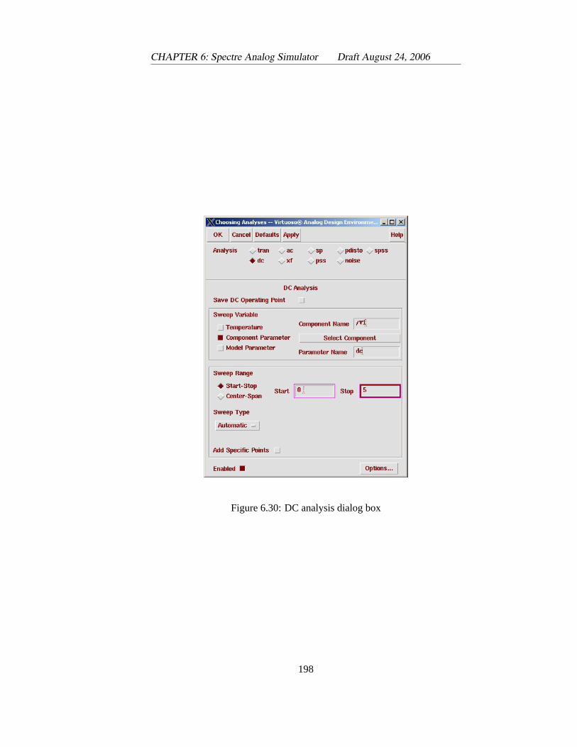
CHAPTER 6: Spectre Analog Simulator Draft August 24, 2006
Figure 6.30: DC analysis dialog box
198
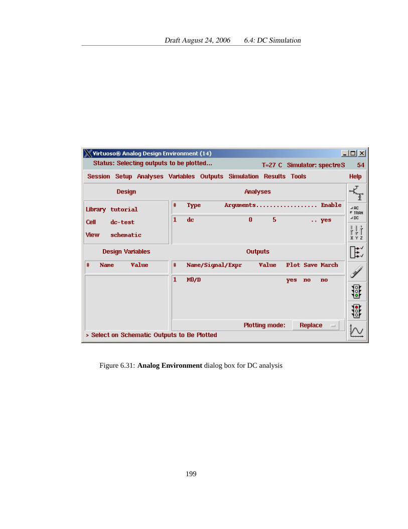
Draft August 24, 2006 6.4: DC Simulation
Figure 6.31:Analog Environment dialog box for DC analysis
199
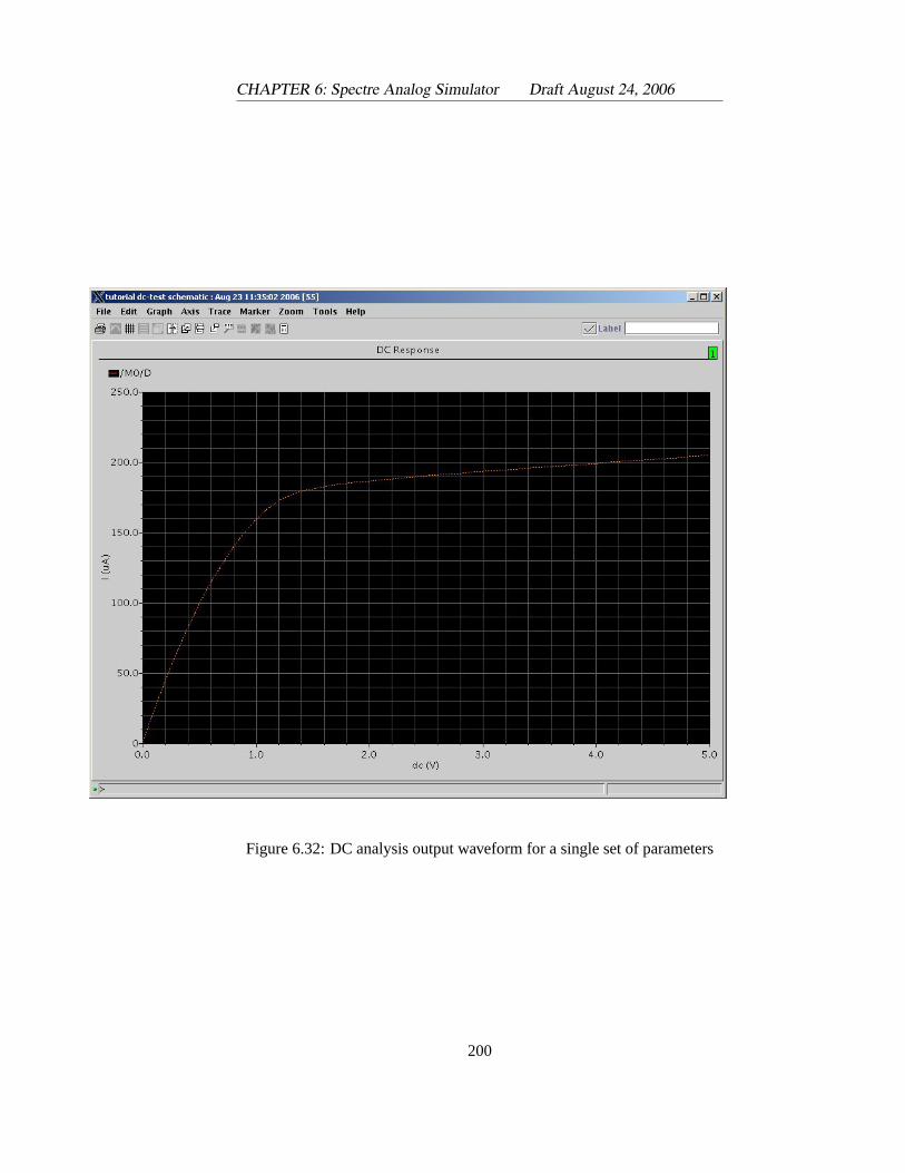
CHAPTER 6: Spectre Analog Simulator Draft August 24, 2006
Figure 6.32: DC analysis output waveform for a single set of parameters
200
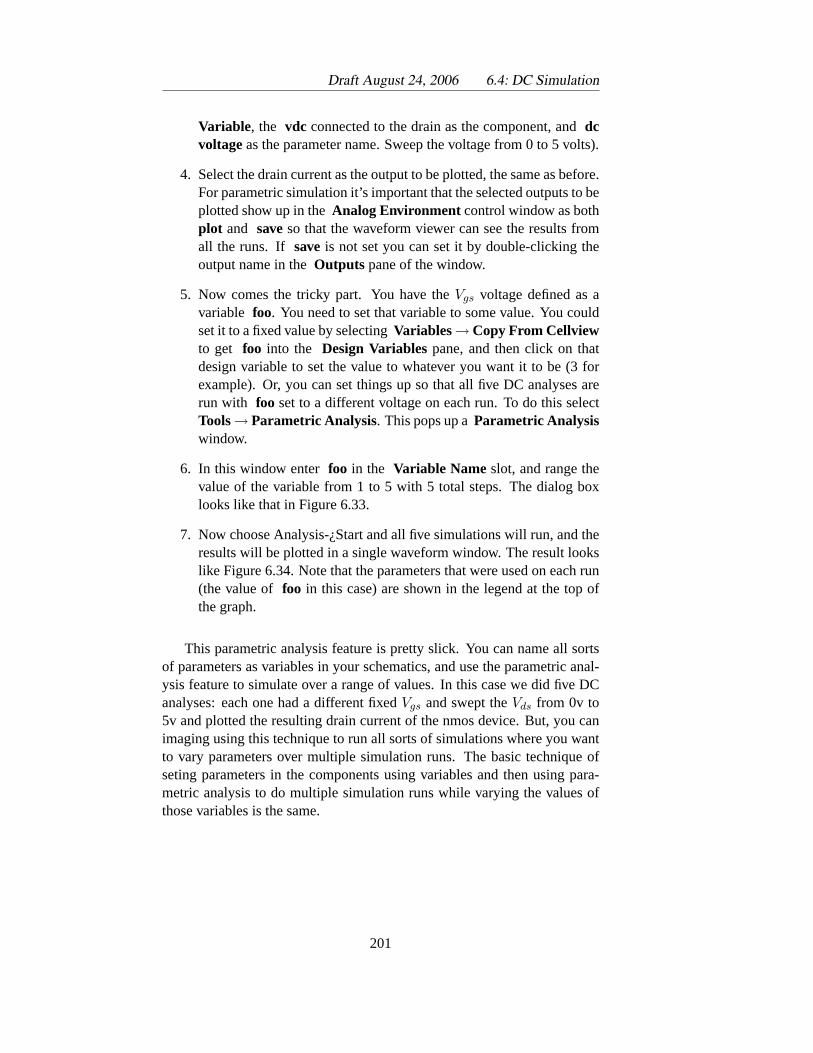
Draft August 24, 2006 6.4: DC Simulation
Variable, the vdc connected to the drain as the component, anddcvoltageas the parameter name. Sweep the voltage from 0 to 5 volts).
4. Select the drain current as the output to be plotted, the same as before.For parametric simulation it’s important that the selected outputs to beplotted show up in theAnalog Environment control window as bothplot and saveso that the waveform viewer can see the results fromall the runs. If saveis not set you can set it by double-clicking theoutput name in theOutputs pane of the window.
5. Now comes the tricky part. You have theVgs voltage defined as avariable foo. You need to set that variable to some value. You couldset it to a fixed value by selectingVariables→Copy From Cellviewto get foo into the Design Variablespane, and then click on thatdesign variable to set the value to whatever you want it to be (3 forexample). Or, you can set things up so that all five DC analyses arerun with foo set to a different voltage on each run. To do this selectTools→ Parametric Analysis. This pops up aParametric Analysiswindow.
6. In this window enterfoo in the Variable Name slot, and range thevalue of the variable from 1 to 5 with 5 total steps. The dialog boxlooks like that in Figure 6.33.
7. Now choose Analysis-¿Start and all five simulations will run, and theresults will be plotted in a single waveform window. The result lookslike Figure 6.34. Note that the parameters that were used on each run(the value of foo in this case) are shown in the legend at the top ofthe graph.
This parametric analysis feature is pretty slick. You can name all sortsof parameters as variables in your schematics, and use the parametric anal-ysis feature to simulate over a range of values. In this case we did five DCanalyses: each one had a different fixedVgs and swept theVds from 0v to5v and plotted the resulting drain current of the nmos device. But, you canimaging using this technique to run all sorts of simulations where you wantto vary parameters over multiple simulation runs. The basic technique ofseting parameters in the components using variables and then using para-metric analysis to do multiple simulation runs while varying the values ofthose variables is the same.
201
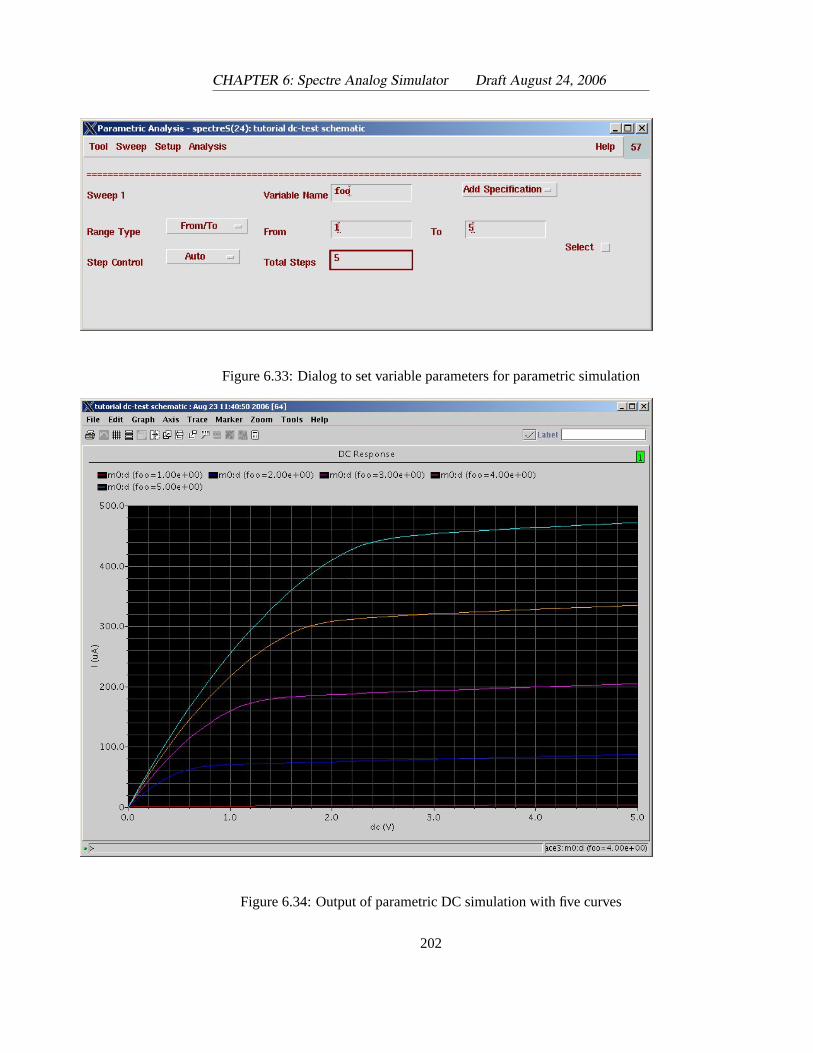
CHAPTER 6: Spectre Analog Simulator Draft August 24, 2006
Figure 6.33: Dialog to set variable parameters for parametric simulation
Figure 6.34: Output of parametric DC simulation with five curves
202

Chapter 7
Cell Characterization
STANDARD CELLS must be characterized so that they can be under-stood and used by the various tools in the CAD flow. So far if you’vedesigned schematic and layout views of your cells the tools under-
stand the transistor netlist and the layout of the cells, but they don’t under-stand the function of the cells in a way that the tools can use, and otherinformation such as the input load, speed, and power of the cell has notbeen extracted in a way that the tools can understand. The synthesis toolscoming up in Chapter 8, for example, need to know the logic function of thecell, the load that the cell input will present to a signal connecting to it, thespeed of the cell under different input slope and output loading conditions,the power that the cell will consume, and the area of the cell in order to doa good job of synthesizing a behavioral description to a collection of stan-dard cells. Cell characterization is a process of simulating a standard cellwith an analog simulator to extract this information in a way that the othertools can understand. This can be done through specific analog simulation(using SpectreS) whose output you look at to generate the characteriza-tion data, or by using a library characterization tool. In this case we’ll useSignalStorm from Cadence.
7.1 Liberty file format
We need to encode the cell characterization data in a standard format calledliberty format which usually uses a .lib file extension. Liberty format isan ASCII file that describes a cell’s characterized data in a standard way.This file is used both by the synthesis tools described in Chapter 8 and bythe place and route tools in Chapter 10. The general form of a liberty fileis shown in Figure 7.1. At this level of detail it simply describes the overallstructure of the file. Each field has lots of detail that you can add by hand, or
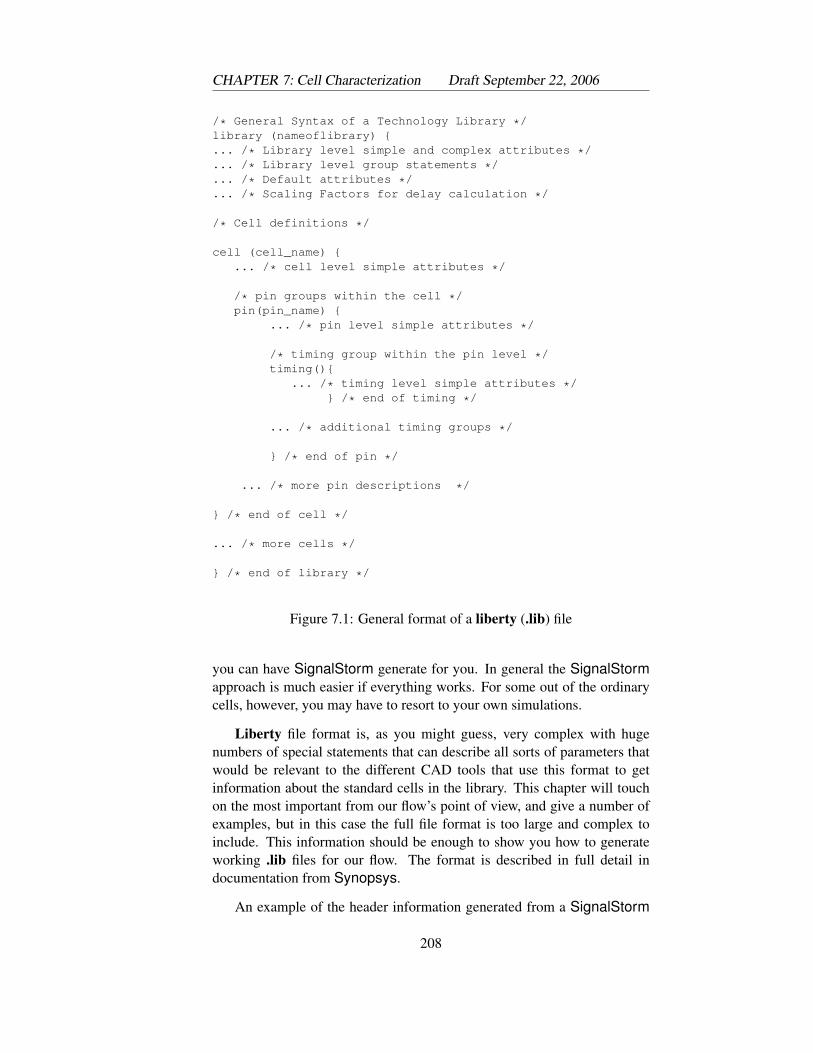
CHAPTER 7: Cell Characterization Draft September 22, 2006
/* General Syntax of a Technology Library */library (nameoflibrary) {... /* Library level simple and complex attributes */... /* Library level group statements */... /* Default attributes */... /* Scaling Factors for delay calculation */
/* Cell definitions */
cell (cell_name) {... /* cell level simple attributes */
/* pin groups within the cell */pin(pin_name) {
... /* pin level simple attributes */
/* timing group within the pin level */timing(){
... /* timing level simple attributes */} /* end of timing */
... /* additional timing groups */
} /* end of pin */
... /* more pin descriptions */
} /* end of cell */
... /* more cells */
} /* end of library */
Figure 7.1: General format of a liberty (.lib) file
you can have SignalStorm generate for you. In general the SignalStormapproach is much easier if everything works. For some out of the ordinarycells, however, you may have to resort to your own simulations.
Liberty file format is, as you might guess, very complex with hugenumbers of special statements that can describe all sorts of parameters thatwould be relevant to the different CAD tools that use this format to getinformation about the standard cells in the library. This chapter will touchon the most important from our flow’s point of view, and give a number ofexamples, but in this case the full file format is too large and complex toinclude. This information should be enough to show you how to generateworking .lib files for our flow. The format is described in full detail indocumentation from Synopsys.
An example of the header information generated from a SignalStorm
208
Draft September 22, 2006 7.1: Liberty file format
characterization run is shown in Figure 7.2. This is all data above the celldefinitions in the .lib file. Later we will see how to add additional infor-mation to this technology header to generate, for example, a simple modelof wire loads that estimates the delay that will be caused by the RC de-lays in the wiring of the circuit once it is physically placed and routed. Fornow we can look at the information in the header and see what’s going on.The delay model says that the characterized delays will be described intable lookup format. This means that the delays will be described as a ta-ble of delays simulated with different input and output conditions. In ourcharacterizations this will be the input slope on one dimension of the tableand output capacitive load on the other axis. The synthesis tool can usethis information, and information about the connection of the cells that itis synthesizing, to estimate delays with reasonable accuracy (assuming thatthe tables have enough data, and that the data is accurate of course). Thereare other delay models possible, but table lookup is by far the most widelyused.
The in place swap mode tells the tool that uses this file that cells whosefootprints match can be used as replacements for each other. This allowsus to have, for example, inverters with the same logic function but withdifferent output drives swapped for each other as required. To prevent thisswapping you would set this mode to be no swapping.
The unit attributes should be fairly self-explanatory. They define the Delays are measuredwith these percentagesbecause measuring fromthe 50% point can resultin a negative delay. Thiscan happen if a gate hashigh gain so that a smallchange on the inputcauses the output tochange rapidly. By thetime the input has risento 50%, the output hasalready changed.
default units that various electrical parameters will be described in so thatsimple numbers can be used in the cell descriptions with the units assumedto be these defaults. The thresholds define where in the waveform slews anddelays are computed. In this case the rise and fall times are computed at the30-70% points in the input or output waveform. That is, delays are definedas being measured from 30% of the total rise or fall on the input to 70% ofthe rise or fall of the output. The percentages are based on vdd. The defaultoperating conditions are set which are actually only really useful if multipleoperating conditions are characterized (usually typical, max, and min) but,of course, that increases characterization time. Finally the format of thelu table template is defined for both delay and power computations. Theseare the look up tables that will contain the actual timing and power data.In this case we define 5x5 tables with input slope (input net transition)on the first axis and output capacitance (total output net capacitance) onthe second axis. The actual value of the input slope (in ns) and the outputloading (in pF) will be defined for each look up table defined in the celldefinition section.
209
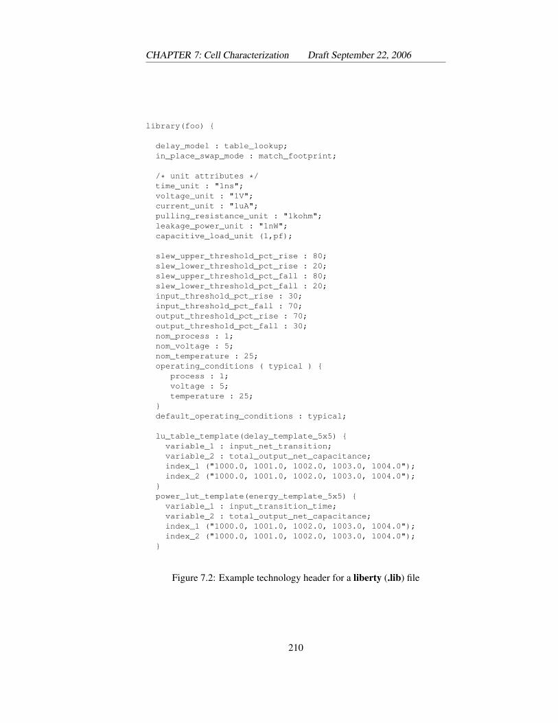
CHAPTER 7: Cell Characterization Draft September 22, 2006
library(foo) {
delay_model : table_lookup;in_place_swap_mode : match_footprint;
/* unit attributes */time_unit : "1ns";voltage_unit : "1V";current_unit : "1uA";pulling_resistance_unit : "1kohm";leakage_power_unit : "1nW";capacitive_load_unit (1,pf);
slew_upper_threshold_pct_rise : 80;slew_lower_threshold_pct_rise : 20;slew_upper_threshold_pct_fall : 80;slew_lower_threshold_pct_fall : 20;input_threshold_pct_rise : 30;input_threshold_pct_fall : 70;output_threshold_pct_rise : 70;output_threshold_pct_fall : 30;nom_process : 1;nom_voltage : 5;nom_temperature : 25;operating_conditions ( typical ) {
process : 1;voltage : 5;temperature : 25;
}default_operating_conditions : typical;
lu_table_template(delay_template_5x5) {variable_1 : input_net_transition;variable_2 : total_output_net_capacitance;index_1 ("1000.0, 1001.0, 1002.0, 1003.0, 1004.0");index_2 ("1000.0, 1001.0, 1002.0, 1003.0, 1004.0");
}power_lut_template(energy_template_5x5) {variable_1 : input_transition_time;variable_2 : total_output_net_capacitance;index_1 ("1000.0, 1001.0, 1002.0, 1003.0, 1004.0");index_2 ("1000.0, 1001.0, 1002.0, 1003.0, 1004.0");
}
Figure 7.2: Example technology header for a liberty (.lib) file
210
Draft September 22, 2006 7.1: Liberty file format
Wire Load Models
An increasingly important contributor to the overall delay in a circuit is thedelay in the wires. For a simple model of wire delay it’s not too hard tocompute the wire’s contribution to delay once the wiring is actually known(i.e. after place and route). But, if you’re using information in the .lib file toestimate performance before you have physical placement and wiring, howdo you estimate the wire delays? One way is to use an educated guess atthe average length of a wire for a broad class of circuits of different sizes.It turns out that, not surprisingly, average wires tend to get longer the largerthe circuit is. When a program like Synopsys generates a circuit from abehavioral description, it has information from the .lib file about the sizeof the cells, so it has a good estimate of what the final size of the circuitmight be. Using that circuit size, a wire load model can be used to estimate(roughly) what the wire delay will be for the final circuit.
A good wire load model might come from a company where many de-signs have been done using a particular cell library, and statistics have beenkept on the average wire length for circuits build using those libraries. Wedon’t have such good statistics for our library so we’ll have to guess. Thewire load model in Figures 7.3 and 7.3 define a wire load model derivedfrom some rough guesses about wire length and some information about theresistance and capacitance of general wiring in our 0.6µ CMOS process.These models would be placed in the .lib file right after the technology in-formation in Figure 7.2.
7.1.1 Combinational Cell Definition
The cell definition (with some details deleted so it fits on a page) that wasderived from the SignalStorm characterization for an inverter is shown inFigure 7.5. You can see that the name of the cell is INVX1 and the overallattributes are defined. Then each pin is described. Pin A is an input pin soits attributes are all related to the capacitance that this pin presents to anysignal that connects to it. Remember the default units earlier in the file sothese numbers are in units of pF.
The output pin Y is much more interesting. Delays occur at the outputpins with respect to changes on the input pins and hence only output pinshave timing information for combinational cells. Because it doesn’t feedback into the cell the capacitance that output pin Y sees because of this cellis 0. The function of the output defines the logical behavior of the cell.In this case the function is !A or the inverse of the A input. The timing()section defines how the output timing relates to changes on each input pin.There’s only one input pin in this case but for a gate with multiple inputs the
211
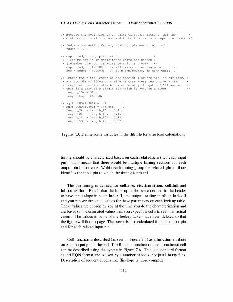
CHAPTER 7: Cell Characterization Draft September 22, 2006
/* Because the cell area is in units of square microns, all the ** distance units will be assumed to be in microns or square microns. */
/* fudge = correction factor, routing, placement, etc. */fudge = 1.0;
/* cap = fudge * cap per micron ** I assume cap is in capacitance units per micron ** (remember that our capacitance unit is 1.0pf) */
cap = fudge * 0.000030; /* .03ff/micron for avg metal */res = fudge * 0.00008 /* 80 m-ohm/square, in kohm units */
/* length_top = the length of one side of a square die (in our case, ** a 4 TCU die of 2500u on a side of core area) length_10k = the ** length of one side of a block containing 10k gates (I’ll assume ** this is a core of a single TCU which is 900u on a side) */
length_10k = 900;length_top = 2500.0;
/* sqrt(5000/10000) = .71 ** sqrt(2000/10000) = .45 etc */
length_5k = length_10k * 0.71;length_2k = length_10k * 0.45;length_1k = length_10k * 0.32;length_500 = length_10k * 0.22;
Figure 7.3: Define some variables in the .lib file for wire load calculations
timing should be characterized based on each related pin (i.e. each inputpin). This means that there would be multiple timing sections for eachoutput pin in that case. Within each timing group the related pin attributeidentifies the input pin to which the timing is related.
The pin timing is defined for cell rise, rise transition, cell fall andfall transition. Recall that the look up tables were defined in the headerto have input slope in ns on index 1, and output loading in pF on index 2and you can see the actual values for these parameters on each look up table.These values are chosen by you at the time you do the characterization andare based on the estimated values that you expect the cells to see in an actualcircuit. The values in some of the lookup tables have been deleted so thatthe figure will fit on a page. The power is also calculated for each output pinand for each related input pin.
Cell function is described (as seen in Figure 7.5) as a function attributeon each output pin of the cell. The Boolean function of a combinational cellcan be described using the syntax in Figure 7.6. This is a standard formatcalled EQN format and is used by a number of tools, not just liberty files.Description of sequential cells like flip-flops is more complex.
212
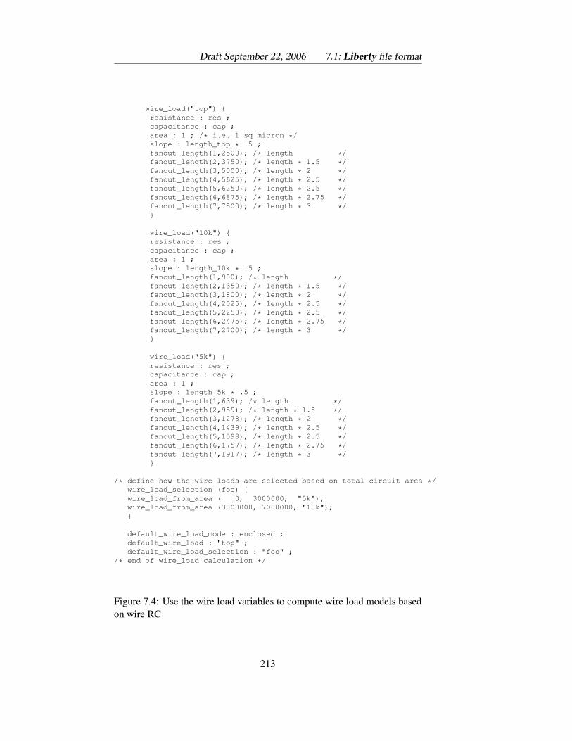
Draft September 22, 2006 7.1: Liberty file format
wire_load("top") {resistance : res ;capacitance : cap ;area : 1 ; /* i.e. 1 sq micron */slope : length_top * .5 ;fanout_length(1,2500); /* length */fanout_length(2,3750); /* length * 1.5 */fanout_length(3,5000); /* length * 2 */fanout_length(4,5625); /* length * 2.5 */fanout_length(5,6250); /* length * 2.5 */fanout_length(6,6875); /* length * 2.75 */fanout_length(7,7500); /* length * 3 */}
wire_load("10k") {resistance : res ;capacitance : cap ;area : 1 ;slope : length_10k * .5 ;fanout_length(1,900); /* length */fanout_length(2,1350); /* length * 1.5 */fanout_length(3,1800); /* length * 2 */fanout_length(4,2025); /* length * 2.5 */fanout_length(5,2250); /* length * 2.5 */fanout_length(6,2475); /* length * 2.75 */fanout_length(7,2700); /* length * 3 */}
wire_load("5k") {resistance : res ;capacitance : cap ;area : 1 ;slope : length_5k * .5 ;fanout_length(1,639); /* length */fanout_length(2,959); /* length * 1.5 */fanout_length(3,1278); /* length * 2 */fanout_length(4,1439); /* length * 2.5 */fanout_length(5,1598); /* length * 2.5 */fanout_length(6,1757); /* length * 2.75 */fanout_length(7,1917); /* length * 3 */}
/* define how the wire loads are selected based on total circuit area */wire_load_selection (foo) {wire_load_from_area ( 0, 3000000, "5k");wire_load_from_area (3000000, 7000000, "10k");}
default_wire_load_mode : enclosed ;default_wire_load : "top" ;default_wire_load_selection : "foo" ;
/* end of wire_load calculation */
Figure 7.4: Use the wire load variables to compute wire load models basedon wire RC
213
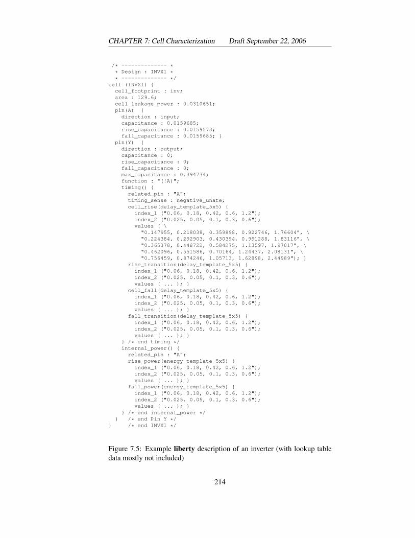
CHAPTER 7: Cell Characterization Draft September 22, 2006
/* -------------- ** Design : INVX1 ** -------------- */
cell (INVX1) {cell_footprint : inv;area : 129.6;cell_leakage_power : 0.0310651;pin(A) {
direction : input;capacitance : 0.0159685;rise_capacitance : 0.0159573;fall_capacitance : 0.0159685; }
pin(Y) {direction : output;capacitance : 0;rise_capacitance : 0;fall_capacitance : 0;max_capacitance : 0.394734;function : "(!A)";timing() {
related_pin : "A";timing_sense : negative_unate;cell_rise(delay_template_5x5) {
index_1 ("0.06, 0.18, 0.42, 0.6, 1.2");index_2 ("0.025, 0.05, 0.1, 0.3, 0.6");values ( \
"0.147955, 0.218038, 0.359898, 0.922746, 1.76604", \"0.224384, 0.292903, 0.430394, 0.991288, 1.83116", \"0.365378, 0.448722, 0.584275, 1.13597, 1.97017", \"0.462096, 0.551586, 0.70164, 1.24437, 2.08131", \"0.756459, 0.874246, 1.05713, 1.62898, 2.44989"); }
rise_transition(delay_template_5x5) {index_1 ("0.06, 0.18, 0.42, 0.6, 1.2");index_2 ("0.025, 0.05, 0.1, 0.3, 0.6");values ( ... ); }
cell_fall(delay_template_5x5) {index_1 ("0.06, 0.18, 0.42, 0.6, 1.2");index_2 ("0.025, 0.05, 0.1, 0.3, 0.6");values ( ... ); }
fall_transition(delay_template_5x5) {index_1 ("0.06, 0.18, 0.42, 0.6, 1.2");index_2 ("0.025, 0.05, 0.1, 0.3, 0.6");values ( ... ); }
} /* end timing */internal_power() {
related_pin : "A";rise_power(energy_template_5x5) {
index_1 ("0.06, 0.18, 0.42, 0.6, 1.2");index_2 ("0.025, 0.05, 0.1, 0.3, 0.6");values ( ... ); }
fall_power(energy_template_5x5) {index_1 ("0.06, 0.18, 0.42, 0.6, 1.2");index_2 ("0.025, 0.05, 0.1, 0.3, 0.6");values ( ... ); }
} /* end internal_power */} /* end Pin Y */
} /* end INVX1 */
Figure 7.5: Example liberty description of an inverter (with lookup tabledata mostly not included)
214
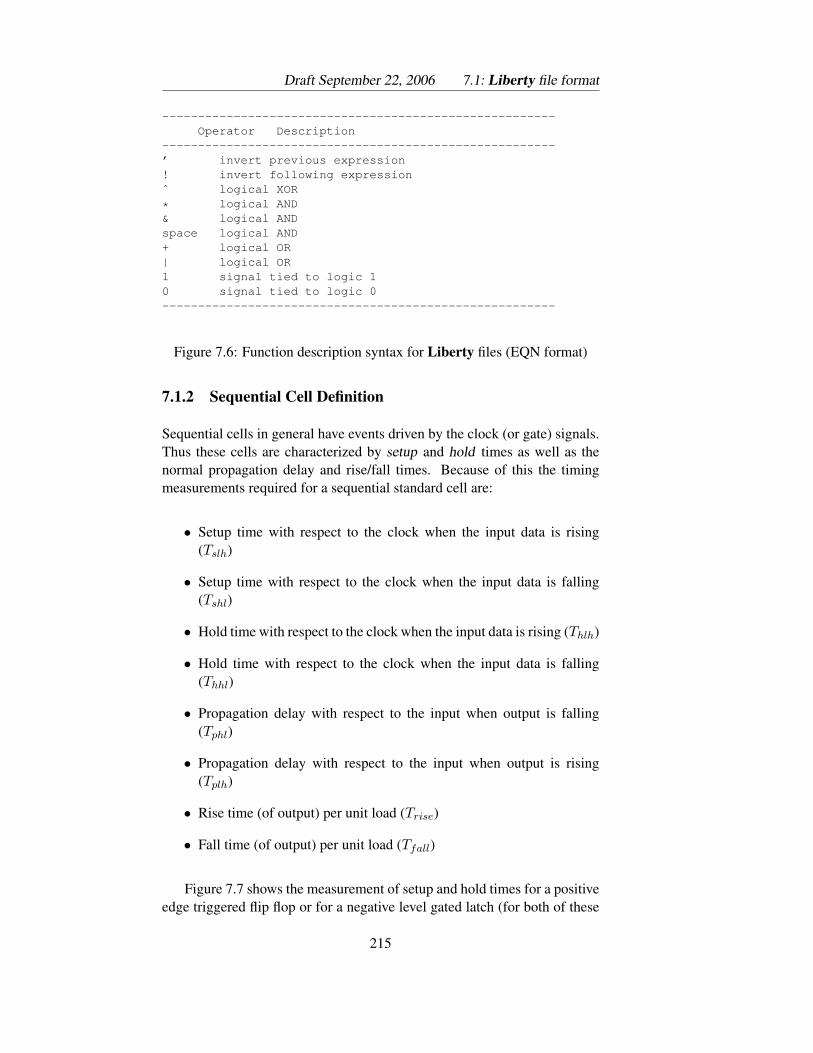
Draft September 22, 2006 7.1: Liberty file format
-------------------------------------------------------Operator Description
-------------------------------------------------------’ invert previous expression! invert following expressionˆ logical XOR
* logical AND& logical ANDspace logical AND+ logical OR| logical OR1 signal tied to logic 10 signal tied to logic 0-------------------------------------------------------
Figure 7.6: Function description syntax for Liberty files (EQN format)
7.1.2 Sequential Cell Definition
Sequential cells in general have events driven by the clock (or gate) signals.Thus these cells are characterized by setup and hold times as well as thenormal propagation delay and rise/fall times. Because of this the timingmeasurements required for a sequential standard cell are:
• Setup time with respect to the clock when the input data is rising(Tslh)
• Setup time with respect to the clock when the input data is falling(Tshl)
• Hold time with respect to the clock when the input data is rising (Thlh)
• Hold time with respect to the clock when the input data is falling(Thhl)
• Propagation delay with respect to the input when output is falling(Tphl)
• Propagation delay with respect to the input when output is rising(Tplh)
• Rise time (of output) per unit load (Trise)
• Fall time (of output) per unit load (Tfall)
Figure 7.7 shows the measurement of setup and hold times for a positiveedge triggered flip flop or for a negative level gated latch (for both of these
215
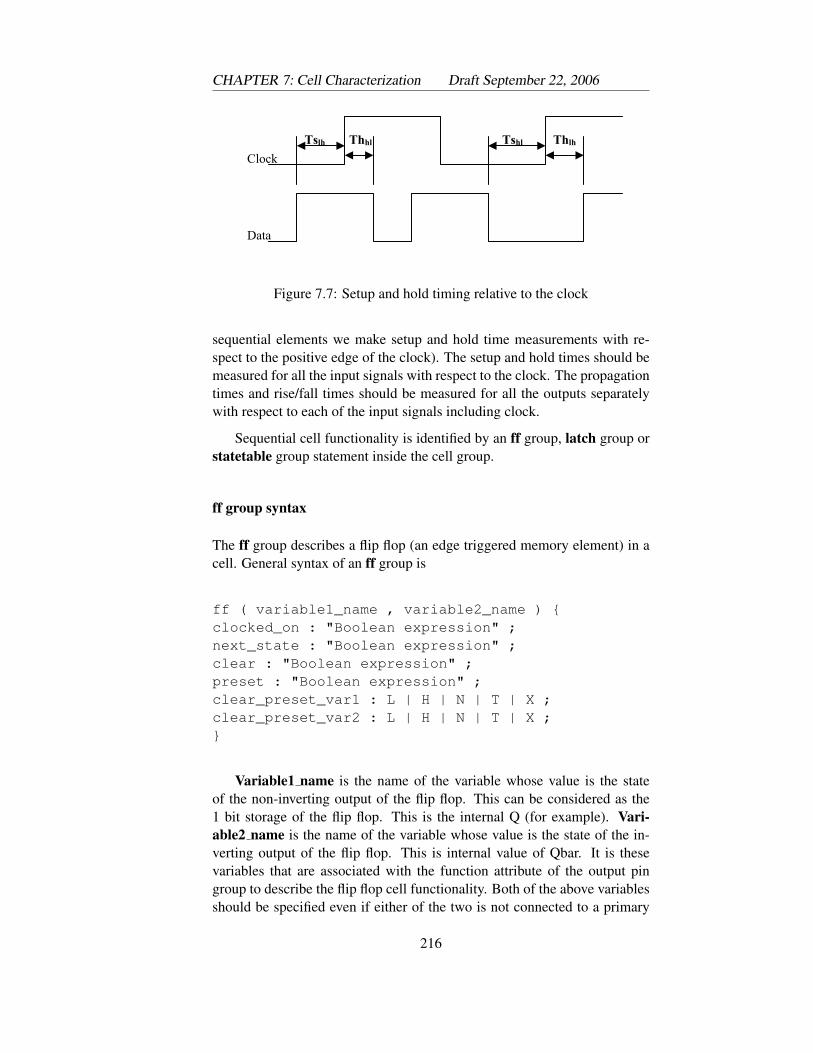
CHAPTER 7: Cell Characterization Draft September 22, 2006
Clock
Data
Tslh Thhl Tshl Thlh
Figure 7.7: Setup and hold timing relative to the clock
sequential elements we make setup and hold time measurements with re-spect to the positive edge of the clock). The setup and hold times should bemeasured for all the input signals with respect to the clock. The propagationtimes and rise/fall times should be measured for all the outputs separatelywith respect to each of the input signals including clock.
Sequential cell functionality is identified by an ff group, latch group orstatetable group statement inside the cell group.
ff group syntax
The ff group describes a flip flop (an edge triggered memory element) in acell. General syntax of an ff group is
ff ( variable1_name , variable2_name ) {clocked_on : "Boolean expression" ;next_state : "Boolean expression" ;clear : "Boolean expression" ;preset : "Boolean expression" ;clear_preset_var1 : L | H | N | T | X ;clear_preset_var2 : L | H | N | T | X ;}
Variable1 name is the name of the variable whose value is the stateof the non-inverting output of the flip flop. This can be considered as the1 bit storage of the flip flop. This is the internal Q (for example). Vari-able2 name is the name of the variable whose value is the state of the in-verting output of the flip flop. This is internal value of Qbar. It is thesevariables that are associated with the function attribute of the output pingroup to describe the flip flop cell functionality. Both of the above variablesshould be specified even if either of the two is not connected to a primary
216
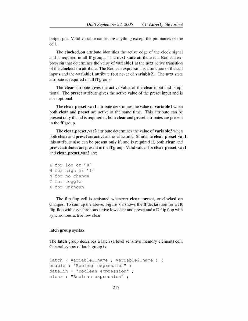
Draft September 22, 2006 7.1: Liberty file format
output pin. Valid variable names are anything except the pin names of thecell.
The clocked on attribute identifies the active edge of the clock signaland is required in all ff groups. The next state attribute is a Boolean ex-pression that determines the value of variable1 at the next active transitionof the clocked on attribute. The Boolean expression is a function of the cellinputs and the variable1 attribute (but never of variable2). The next stateattribute is required in all ff groups.
The clear attribute gives the active value of the clear input and is op-tional. The preset attribute gives the active value of the preset input and isalso optional.
The clear preset var1 attribute determines the value of variable1 whenboth clear and preset are active at the same time. This attribute can bepresent only if, and is required if, both clear and preset attributes are presentin the ff group.
The clear preset var2 attribute determines the value of variable2 whenboth clear and preset are active at the same time. Similar to clear preset var1,this attribute also can be present only if, and is required if, both clear andpreset attributes are present in the ff group. Valid values for clear preset var1and clear preset var2 are:
L for low or ’0’H for high or ’1’N for no changeT for toggleX for unknown
The flip-flop cell is activated whenever clear, preset, or clocked onchanges. To sum up the above, Figure 7.8 shows the ff declaration for a JKflip-flop with asynchronous active low clear and preset and a D flip flop withsynchronous active low clear.
latch group syntax
The latch group describes a latch (a level sensitive memory element) cell.General syntax of latch group is
latch ( variable1_name , variable2_name ) {enable : "Boolean expression" ;data_in : "Boolean expression" ;clear : "Boolean expression" ;
217
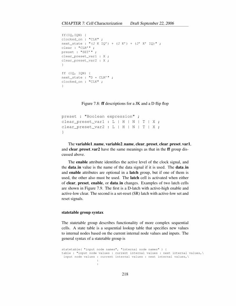
CHAPTER 7: Cell Characterization Draft September 22, 2006
ff(IQ,IQN) {clocked_on : "CLK" ;next_state : "(J K IQ’) + (J K’) + (J’ K’ IQ)" ;clear : "CLR’" ;preset : "SET’" ;clear_preset_var1 : X ;clear_preset_var2 : X ;}
ff (IQ, IQN) {next_state : "D * CLR’" ;clocked_on : "CLK" ;}
Figure 7.8: ff descriptions for a JK and a D flip flop
preset : "Boolean expression" ;clear_preset_var1 : L | H | N | T | X ;clear_preset_var2 : L | H | N | T | X ;}
The variable1 name, variable2 name, clear, preset, clear preset var1,and clear preset var2 have the same meanings as that in the ff group dis-cussed above.
The enable attribute identifies the active level of the clock signal, andthe data in value is the name of the data signal if it is used. The data inand enable attributes are optional in a latch group, but if one of them isused, the other also must be used. The latch cell is activated when eitherof clear, preset, enable, or data in changes. Examples of two latch cellsare shown in Figure 7.9. The first is a D-latch with active-high enable andactive-low clear. The second is a set-reset (SR) latch with active-low set andreset signals.
statetable group syntax
The statetable group describes functionality of more complex sequentialcells. A state table is a sequential lookup table that specifies new valuesto internal nodes based on the current internal node values and inputs. Thegeneral syntax of a statetable group is
statetable( "input node names", "internal node names" ) {table : "input node values : current internal values : next internal values,\input node values : current internal values : next internal values,\
::
218
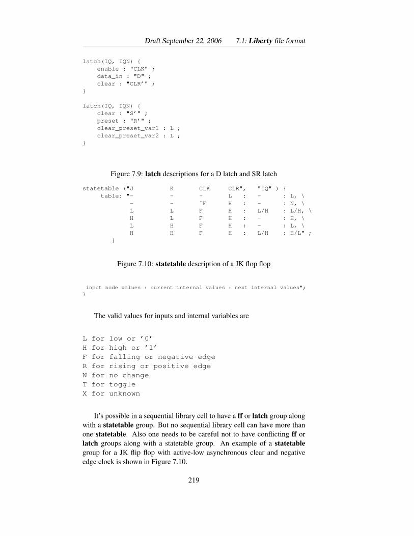
Draft September 22, 2006 7.1: Liberty file format
latch(IQ, IQN) {enable : "CLK" ;data_in : "D" ;clear : "CLR’" ;
}
latch(IQ, IQN) {clear : "S’" ;preset : "R’" ;clear_preset_var1 : L ;clear_preset_var2 : L ;
}
Figure 7.9: latch descriptions for a D latch and SR latch
statetable ("J K CLK CLR", "IQ" ) {table: "- - - L : - : L, \
- - ˜F H : - : N, \L L F H : L/H : L/H, \H L F H : - : H, \L H F H : - : L, \H H F H : L/H : H/L" ;
}
Figure 7.10: statetable description of a JK flop flop
input node values : current internal values : next internal values";}
The valid values for inputs and internal variables are
L for low or ’0’H for high or ’1’F for falling or negative edgeR for rising or positive edgeN for no changeT for toggleX for unknown
It’s possible in a sequential library cell to have a ff or latch group alongwith a statetable group. But no sequential library cell can have more thanone statetable. Also one needs to be careful not to have conflicting ff orlatch groups along with a statetable group. An example of a statetablegroup for a JK flip flop with active-low asynchronous clear and negativeedge clock is shown in Figure 7.10.
219
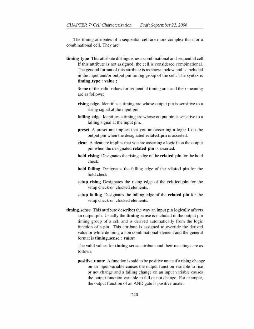
CHAPTER 7: Cell Characterization Draft September 22, 2006
The timing attributes of a sequential cell are more complex than for acombinational cell. They are:
timing type This attribute distinguishes a combinational and sequential cell.If this attribute is not assigned, the cell is considered combinational.The general format of this attribute is as shown below and is includedin the input and/or output pin timing group of the cell. The syntax istiming type : value ;
Some of the valid values for sequential timing arcs and their meaningare as follows:
rising edge Identifies a timing arc whose output pin is sensitive to arising signal at the input pin.
falling edge Identifies a timing arc whose output pin is sensitive to afalling signal at the input pin.
preset A preset arc implies that you are asserting a logic 1 on theoutput pin when the designated related pin is asserted.
clear A clear arc implies that you are asserting a logic 0 on the outputpin when the designated related pin is asserted.
hold rising Designates the rising edge of the related pin for the holdcheck.
hold falling Designates the falling edge of the related pin for thehold check.
setup rising Designates the rising edge of the related pin for thesetup check on clocked elements.
setup falling Designates the falling edge of the related pin for thesetup check on clocked elements.
timing sense This attribute describes the way an input pin logically affectsan output pin. Usually the timing sense is included in the output pintiming group of a cell and is derived automatically from the logicfunction of a pin. This attribute is assigned to override the derivedvalue or while defining a non combinational element and the generalformat is timing sense : value;
The valid values for timing sense attribute and their meanings are asfollows:
positive unate A function is said to be positive unate if a rising changeon an input variable causes the output function variable to riseor not change and a falling change on an input variable causesthe output function variable to fall or not change. For example,the output function of an AND gate is positive unate.
220
Draft September 22, 2006 7.1: Liberty file format
negative unate A function is said to be negative unate if a risingchange on an input variable causes the output function variableto fall or not change and a falling change on an input variablecauses the output function variable to rise or not change. Forexample, the output function of a NAND gate is negative unate.
non unate The non unate timing sense represents a function whoseoutput value change cannot be determined from the direction ofthe change in the input value. For example, the output functionof an XOR gate is non unate.
Also note that if a related pin is an output pin, the timing sense at-tribute for that pin must be defined.
clock This attribute is optional and indicates whether an input pin is a clockpin. The syntax is clock : true; or clock : false;
min period This is an optional attribute on the clock pin of a flip flop orlatch specifies the minimum clock period required for the input pin.The syntax is min period : value;
A D-type edge triggered flip flop can be described in terms of all theseattributes. The .lib description (with the data in the lookup tables missingso that it will fit on a page) is shown in Figure 7.11. Note that in this casethe setup and hold timing are defined as scalar types, but they could justas easily (well, not really just as easily because there would be extra sim-ulation involved) be described in a lookup table too. The first part of theflip flop description is an ff block describing the functionality. Then the pindescriptions follow. The D input pin had setup and hold timing. The clkpin is defined as a clock, and the Q pin has rise and fall timing described aslookup tables and has timing described with both clk and clr as related pins.The timing values are defined as 5 x 5 lookup tables as seen in Figure 7.5.
7.1.3 Tristate Cell Definition
The major difference of a tristate cell to other cells is that a tristate celloutput can take a value of Z as well as 1 and 0. The output goes to the Zvalue when the cell enable pin is de-asserted or when the tristate condition(generally a Boolean expression) is true. Electrically this Z value is a highimpedance value on the output. It is as if the output drivers are disconnectedfrom the output wire. It is also worthwhile to note that both combinationaltristate cells as well as sequential tristate cells exist.
The type of measurements required for tristate cells are the same asany other combinational or sequential cells. However when it comes to
221
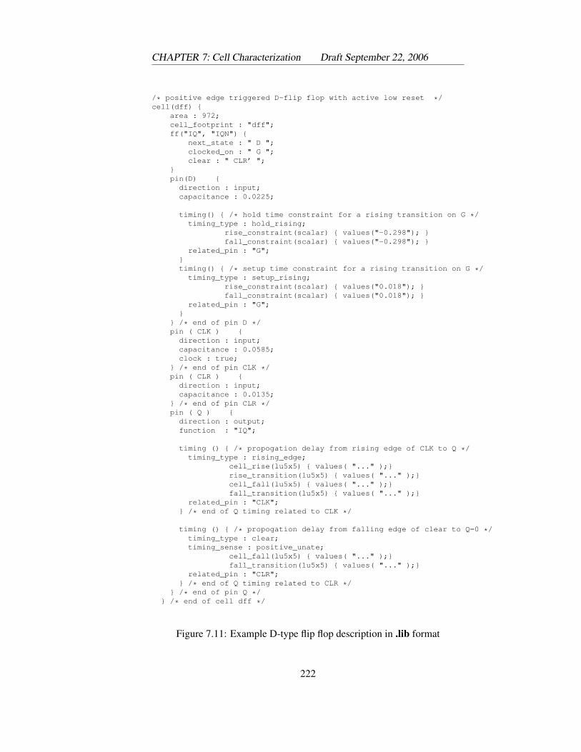
CHAPTER 7: Cell Characterization Draft September 22, 2006
/* positive edge triggered D-flip flop with active low reset */cell(dff) {
area : 972;cell_footprint : "dff";ff("IQ", "IQN") {
next_state : " D ";clocked_on : " G ";clear : " CLR’ ";
}pin(D) {
direction : input;capacitance : 0.0225;
timing() { /* hold time constraint for a rising transition on G */timing_type : hold_rising;
rise_constraint(scalar) { values("-0.298"); }fall_constraint(scalar) { values("-0.298"); }
related_pin : "G";}timing() { /* setup time constraint for a rising transition on G */
timing_type : setup_rising;rise_constraint(scalar) { values("0.018"); }fall_constraint(scalar) { values("0.018"); }
related_pin : "G";}
} /* end of pin D */pin ( CLK ) {
direction : input;capacitance : 0.0585;clock : true;
} /* end of pin CLK */pin ( CLR ) {
direction : input;capacitance : 0.0135;
} /* end of pin CLR */pin ( Q ) {
direction : output;function : "IQ";
timing () { /* propogation delay from rising edge of CLK to Q */timing_type : rising_edge;
cell_rise(lu5x5) { values( "..." );}rise_transition(lu5x5) { values( "..." );}cell_fall(lu5x5) { values( "..." );}fall_transition(lu5x5) { values( "..." );}
related_pin : "CLK";} /* end of Q timing related to CLK */
timing () { /* propogation delay from falling edge of clear to Q=0 */timing_type : clear;timing_sense : positive_unate;
cell_fall(lu5x5) { values( "..." );}fall_transition(lu5x5) { values( "..." );}
related_pin : "CLR";} /* end of Q timing related to CLR */
} /* end of pin Q */} /* end of cell dff */
Figure 7.11: Example D-type flip flop description in .lib format
222
Draft September 22, 2006 7.2: Cell Characterization with SignalStorm
measurement of the tristate output pin parameters with respect to the cellenable pin (or pin related to the tristate condition), one needs to rememberthat either the initial output value or the final output value will be Z. Alsotwo sets of measurements are required with respect to the cell enable pin:one when the cell is being enabled (output going to 1 or 1) and one whenthe cell is being disabled (output going to Z). This makes measurement oftime-to-reach-tristate and time-to-start-driving a little tricky. If the outputsare not connected to capacitors the analog simulator generally simulatorputs the output of a tri-stated device at around 2.5v for a 5v process, so wecan measure from this point when measuring the time to or from a tristateoutput state (or some percentage of that point if you’re using a 10% to 90%measurement, for example).
Special attributes for a tristate gate include
three state This attribute defines a tristate output pin in a cell. The syntaxis three state : <Boolean-expression> ;
The Boolean expression is the condition to make the correspondingoutput pin to go to tristate or high impedance condition.
three state enable This is the value the timing type attribute should takefor the tristatable output pin in the “cell being enabled” timing group.The cell rise and rise transition will correspond to the Z to 1 transi-tion, and the cell fall and fall transition will correspond to the Z to0 transition.
three state disable This is the value then timing type attribute should takefor the tristatable output pin in the “cell being disabled” timing group.The cell rise and rise transition will correspond to the 0 to Z transi-tion, and the cell fall and fall transition will correspond to the 1 toZ transition.
An example of a tristate inverter is shown in Figure 7.12. Note that theenable and disable timing matrix templates are different than the “regular”delay value matrix template. The indices of these templates should havebeen defined in the technology header of the .lib file (see Figure 7.2), orthe actual index values can be defined before each values statement in thetiming block (as they were for the inverter in Figure 7.5).
7.2 Cell Characterization with SignalStorm
SignalStorm is a tool from Cadence that uses Spectre to characterizecells and outputs the results in a format that can be converted into liberty
223
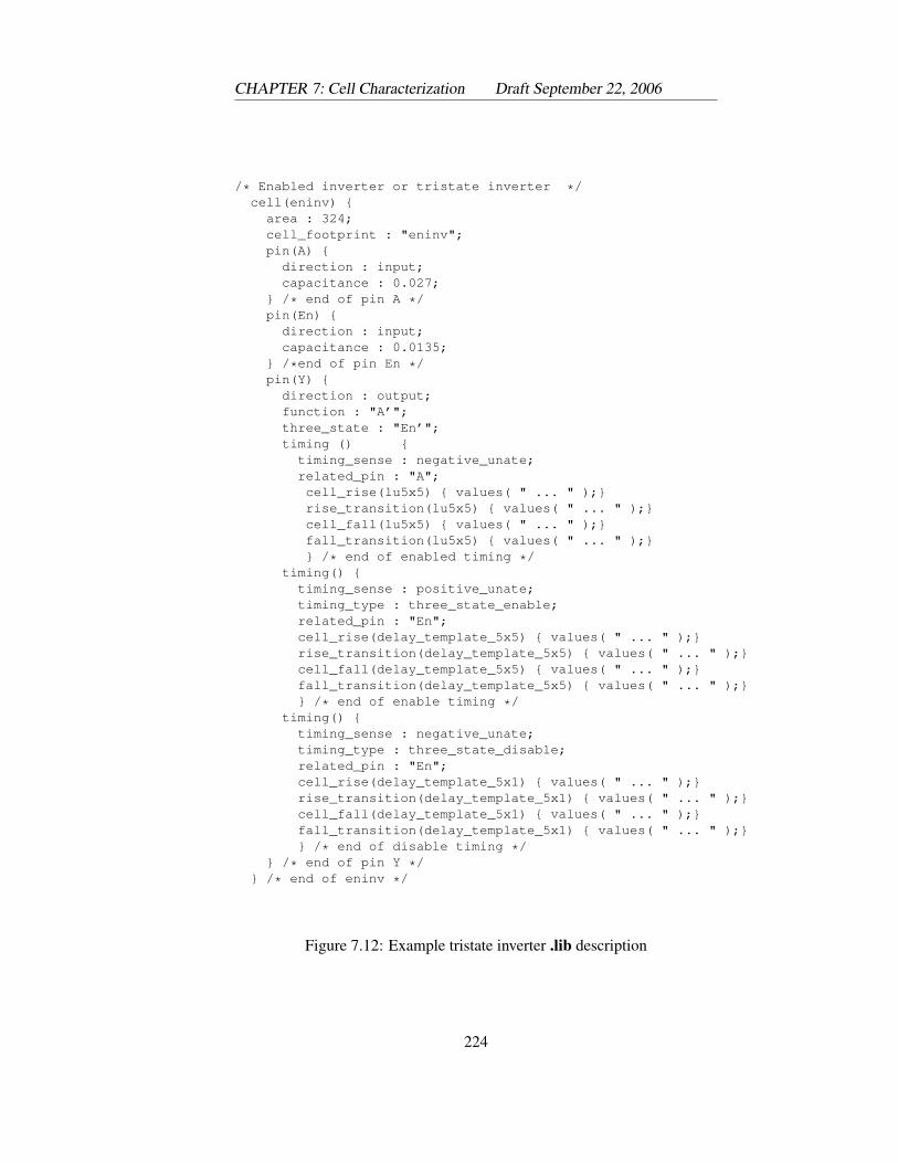
CHAPTER 7: Cell Characterization Draft September 22, 2006
/* Enabled inverter or tristate inverter */cell(eninv) {area : 324;cell_footprint : "eninv";pin(A) {direction : input;capacitance : 0.027;
} /* end of pin A */pin(En) {direction : input;capacitance : 0.0135;
} /*end of pin En */pin(Y) {direction : output;function : "A’";three_state : "En’";timing () {timing_sense : negative_unate;related_pin : "A";cell_rise(lu5x5) { values( " ... " );}rise_transition(lu5x5) { values( " ... " );}cell_fall(lu5x5) { values( " ... " );}fall_transition(lu5x5) { values( " ... " );}} /* end of enabled timing */
timing() {timing_sense : positive_unate;timing_type : three_state_enable;related_pin : "En";cell_rise(delay_template_5x5) { values( " ... " );}rise_transition(delay_template_5x5) { values( " ... " );}cell_fall(delay_template_5x5) { values( " ... " );}fall_transition(delay_template_5x5) { values( " ... " );}} /* end of enable timing */
timing() {timing_sense : negative_unate;timing_type : three_state_disable;related_pin : "En";cell_rise(delay_template_5x1) { values( " ... " );}rise_transition(delay_template_5x1) { values( " ... " );}cell_fall(delay_template_5x1) { values( " ... " );}fall_transition(delay_template_5x1) { values( " ... " );}} /* end of disable timing */
} /* end of pin Y */} /* end of eninv */
Figure 7.12: Example tristate inverter .lib description
224
Draft September 22, 2006 7.2: Cell Characterization with SignalStorm
format. It takes a bit of fiddling to get the inputs just right for this program,mostly because SignalStorm uses pure Spectre format as input whereasthe NCSU tech libraries that are the basis for our cells uses the Spice-styleinput format that SpectreS can read. However, once the input is massagedto the right form this is a very slick program. When you consider that evenfor the inverter, using 5 x 5 timing matrices (25 values each), there are 6 *25 = 150 Spectre runs required to characterize the cell. Each run changesthe input slope or the output loading or both and then measures the inputand output waveform timing to get a number for one of the timing matrices.Cells with larger numbers of inputs and outputs, and sequential cells willrequire even more Spectre runs to characterize. Even a two-input NANDtakes 12 * 25 = 300 Spectre runs for full characterization using 5 x 5 ma-trices.
The other very nice thing about SignalStorm is that it even figures outfor you what the functionality of your cells is. You don’t have to specify inadvance that a cell is, for example, a two-input and-or-invert gate. Signal-Storm will figure this out for you based on analyzing the transistor network.Of course, you need to check to make sure that it has determined the func-tionality correctly, but it’s quite good at this.
7.2.1 Generating the SignalStorm netlist
SignalStorm requires a netlist of all the cells that you would like it to char-acterize. This netlist should be sub-circuit definitions in Spectre format(which is very similar, but not exactly like Spice format). You could writethese by hand, but it’s much more convenient to have Cadence generatethem for you from your schematics. The process will be very similar to thefirst steps of the analog simulation process from Chapter 6, but you’ll haveto specify the Spectre simulator instead of SpectreS, make a few moretweaks, and then stop at netlisting without actually simulating. From there(unfortunately) some hand-modification of the netlist is required.
Before you can characterize a cell you need a cmos sch transistor levelschematic view, and a layout view of each cell you want to characterize.The layout should have passed both DRC and LVS, and you should havecreated an analog extracted view after the LVS was complete. It is theanalog extracted view that we’ll use to generate the transistor netlist forSignalStorm characterization. This is because if you have extracted withparasitic capacitors then the analog extracted view will include not onlyextra information on the transistor sizes, but also those parasitics.
As an example I’ll start with a library that includes the inverter andnand2 cells that you’ve seen from Chapters 3, 4, and 5. The library includes(at least) cmos sch, layout, and analog extracted views of both of these
225
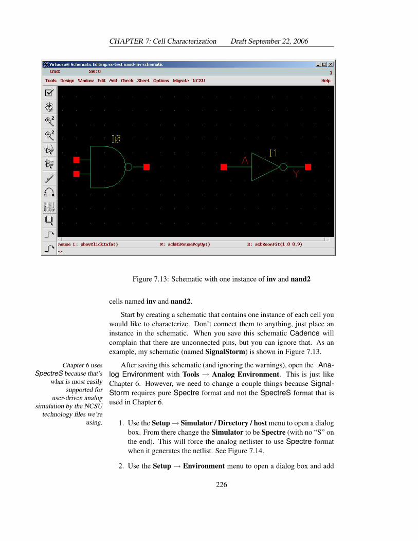
CHAPTER 7: Cell Characterization Draft September 22, 2006
Figure 7.13: Schematic with one instance of inv and nand2
cells named inv and nand2.
Start by creating a schematic that contains one instance of each cell youwould like to characterize. Don’t connect them to anything, just place aninstance in the schematic. When you save this schematic Cadence willcomplain that there are unconnected pins, but you can ignore that. As anexample, my schematic (named SignalStorm) is shown in Figure 7.13.
After saving this schematic (and ignoring the warnings), open the Ana-Chapter 6 usesSpectreS because that’s
what is most easilysupported for
user-driven analogsimulation by the NCSU
technology files we’reusing.
log Environment with Tools → Analog Environment. This is just likeChapter 6. However, we need to change a couple things because Signal-Storm requires pure Spectre format and not the SpectreS format that isused in Chapter 6.
1. Use the Setup→ Simulator / Directory / host menu to open a dialogbox. From there change the Simulator to be Spectre (with no “S” onthe end). This will force the analog netlister to use Spectre formatwhen it generates the netlist. See Figure 7.14.
2. Use the Setup → Environment menu to open a dialog box and add
226
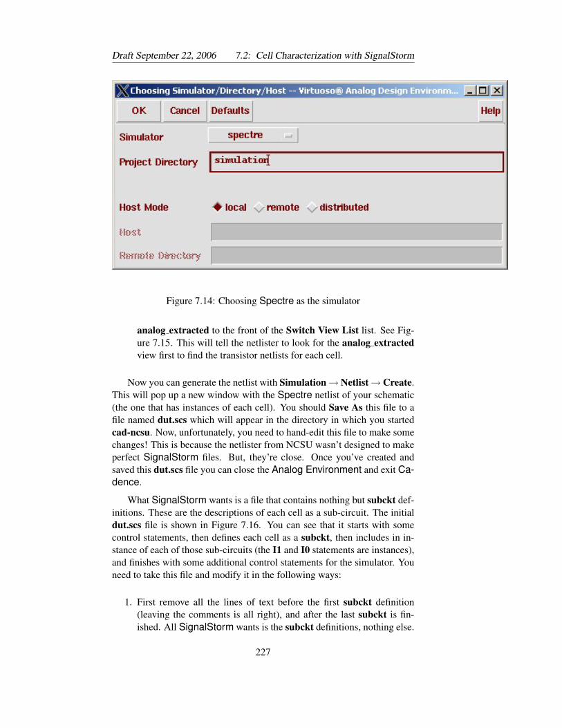
Draft September 22, 2006 7.2: Cell Characterization with SignalStorm
Figure 7.14: Choosing Spectre as the simulator
analog extracted to the front of the Switch View List list. See Fig-ure 7.15. This will tell the netlister to look for the analog extractedview first to find the transistor netlists for each cell.
Now you can generate the netlist with Simulation→Netlist→Create.This will pop up a new window with the Spectre netlist of your schematic(the one that has instances of each cell). You should Save As this file to afile named dut.scs which will appear in the directory in which you startedcad-ncsu. Now, unfortunately, you need to hand-edit this file to make somechanges! This is because the netlister from NCSU wasn’t designed to makeperfect SignalStorm files. But, they’re close. Once you’ve created andsaved this dut.scs file you can close the Analog Environment and exit Ca-dence.
What SignalStorm wants is a file that contains nothing but subckt def-initions. These are the descriptions of each cell as a sub-circuit. The initialdut.scs file is shown in Figure 7.16. You can see that it starts with somecontrol statements, then defines each cell as a subckt, then includes in in-stance of each of those sub-circuits (the I1 and I0 statements are instances),and finishes with some additional control statements for the simulator. Youneed to take this file and modify it in the following ways:
1. First remove all the lines of text before the first subckt definition(leaving the comments is all right), and after the last subckt is fin-ished. All SignalStorm wants is the subckt definitions, nothing else.
227
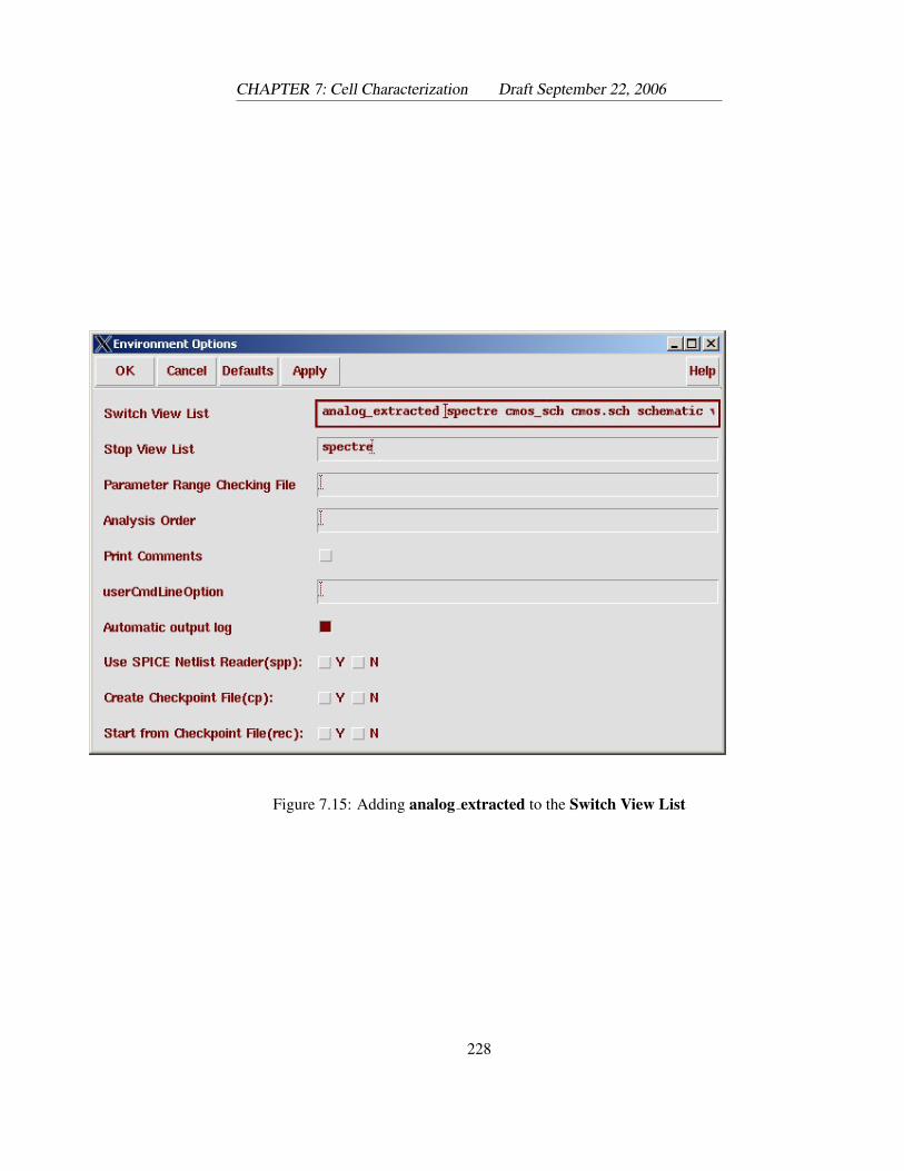
CHAPTER 7: Cell Characterization Draft September 22, 2006
Figure 7.15: Adding analog extracted to the Switch View List
228
Draft September 22, 2006 7.2: Cell Characterization with SignalStorm
Note that Spectre (at least as used by SignalStorm has no conceptof global signals so removing the global statement won’t cause prob-lems.
2. SignalStorm doesn’t like non-alpha characters in signal names. Changeevery instance of vdd! to be vdd.
3. SignalStorm doesn’t like to use 0 as the default ground node. Thisis quite odd because this is a standard convention, but it appears tobe true for the specific way that SignalStorm uses Spectre. Un-fortunately, this is a trickier thing to change with search-and-replacebecause there are also 0’s in other parameters. Make the followingreplacements:
(a) Replace “ 0 ” with “ gnd ” (note that there are spaces on bothsides of each of those strings!).
(b) Replace “(0” with “(gnd”.
(c) Replace “0)” with “gnd)”.
4. Because SignalStorm doesn’t use global signal names, you need toadd vdd gnd to the argument list of each subckt definition.
A dut.scs file that has had all the required modifications is shown inFigure 7.17. Note that it consists only of subckt definitions, has vdd gndadded to all subckt argument lists, and uses vdd and gnd to define the powerand ground connections.
Now that you have a modified dut.scs file with subckt definitions forthe cells you want to characterize, you can start using SignalStorm. I rec-ommend that you make a separate directory in which to run SignalStorm sothat you can compartmentalize things and keep track of where the log filesand result files are. I’m using a $HOME/IC CAD/slc directory for this (slcstands for SignalStorm Library Characterizer). Move your dut.scs file tothat directory.
In your slc directory you need to copy some script files from the classdirectory, specifically the cadence/SLC subdirectory. The directory path is:
/uusoc/facility/cad common/local/class/6710/cadence/SLC
From that directory, copy the step1, step2 and step3 files to your slcdirectory. These are command files you can use to drive the SignalStormcharacterization process. These scripts are used one at a time in sequence,but they represent three important steps in the process where you may needto stop and fix errors which is why they’re separate. You can use the scriptsas-is, or edit them to do different things once you are more familiar withthe process. To run SignalStorm use the cad-slc script in the same
229
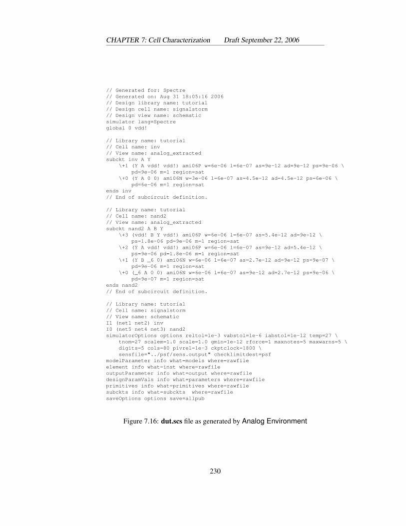
CHAPTER 7: Cell Characterization Draft September 22, 2006
// Generated for: Spectre// Generated on: Aug 31 18:05:16 2006// Design library name: tutorial// Design cell name: signalstorm// Design view name: schematicsimulator lang=Spectreglobal 0 vdd!
// Library name: tutorial// Cell name: inv// View name: analog_extractedsubckt inv A Y
\+1 (Y A vdd! vdd!) ami06P w=6e-06 l=6e-07 as=9e-12 ad=9e-12 ps=9e-06 \pd=9e-06 m=1 region=sat
\+0 (Y A 0 0) ami06N w=3e-06 l=6e-07 as=4.5e-12 ad=4.5e-12 ps=6e-06 \pd=6e-06 m=1 region=sat
ends inv// End of subcircuit definition.
// Library name: tutorial// Cell name: nand2// View name: analog_extractedsubckt nand2 A B Y
\+3 (vdd! B Y vdd!) ami06P w=6e-06 l=6e-07 as=5.4e-12 ad=9e-12 \ps=1.8e-06 pd=9e-06 m=1 region=sat
\+2 (Y A vdd! vdd!) ami06P w=6e-06 l=6e-07 as=9e-12 ad=5.4e-12 \ps=9e-06 pd=1.8e-06 m=1 region=sat
\+1 (Y B _6 0) ami06N w=6e-06 l=6e-07 as=2.7e-12 ad=9e-12 ps=9e-07 \pd=9e-06 m=1 region=sat
\+0 (_6 A 0 0) ami06N w=6e-06 l=6e-07 as=9e-12 ad=2.7e-12 ps=9e-06 \pd=9e-07 m=1 region=sat
ends nand2// End of subcircuit definition.
// Library name: tutorial// Cell name: signalstorm// View name: schematicI1 (net1 net2) invI0 (net5 net4 net3) nand2simulatorOptions options reltol=1e-3 vabstol=1e-6 iabstol=1e-12 temp=27 \
tnom=27 scalem=1.0 scale=1.0 gmin=1e-12 rforce=1 maxnotes=5 maxwarns=5 \digits=5 cols=80 pivrel=1e-3 ckptclock=1800 \sensfile="../psf/sens.output" checklimitdest=psf
modelParameter info what=models where=rawfileelement info what=inst where=rawfileoutputParameter info what=output where=rawfiledesignParamVals info what=parameters where=rawfileprimitives info what=primitives where=rawfilesubckts info what=subckts where=rawfilesaveOptions options save=allpub
Figure 7.16: dut.scs file as generated by Analog Environment
230
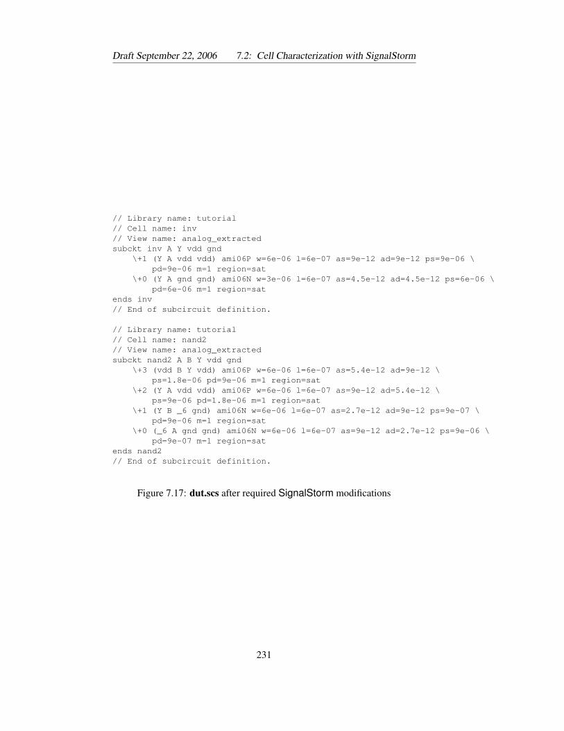
Draft September 22, 2006 7.2: Cell Characterization with SignalStorm
// Library name: tutorial// Cell name: inv// View name: analog_extractedsubckt inv A Y vdd gnd
\+1 (Y A vdd vdd) ami06P w=6e-06 l=6e-07 as=9e-12 ad=9e-12 ps=9e-06 \pd=9e-06 m=1 region=sat
\+0 (Y A gnd gnd) ami06N w=3e-06 l=6e-07 as=4.5e-12 ad=4.5e-12 ps=6e-06 \pd=6e-06 m=1 region=sat
ends inv// End of subcircuit definition.
// Library name: tutorial// Cell name: nand2// View name: analog_extractedsubckt nand2 A B Y vdd gnd
\+3 (vdd B Y vdd) ami06P w=6e-06 l=6e-07 as=5.4e-12 ad=9e-12 \ps=1.8e-06 pd=9e-06 m=1 region=sat
\+2 (Y A vdd vdd) ami06P w=6e-06 l=6e-07 as=9e-12 ad=5.4e-12 \ps=9e-06 pd=1.8e-06 m=1 region=sat
\+1 (Y B _6 gnd) ami06N w=6e-06 l=6e-07 as=2.7e-12 ad=9e-12 ps=9e-07 \pd=9e-06 m=1 region=sat
\+0 (_6 A gnd gnd) ami06N w=6e-06 l=6e-07 as=9e-12 ad=2.7e-12 ps=9e-06 \pd=9e-07 m=1 region=sat
ends nand2// End of subcircuit definition.
Figure 7.17: dut.scs after required SignalStorm modifications
231
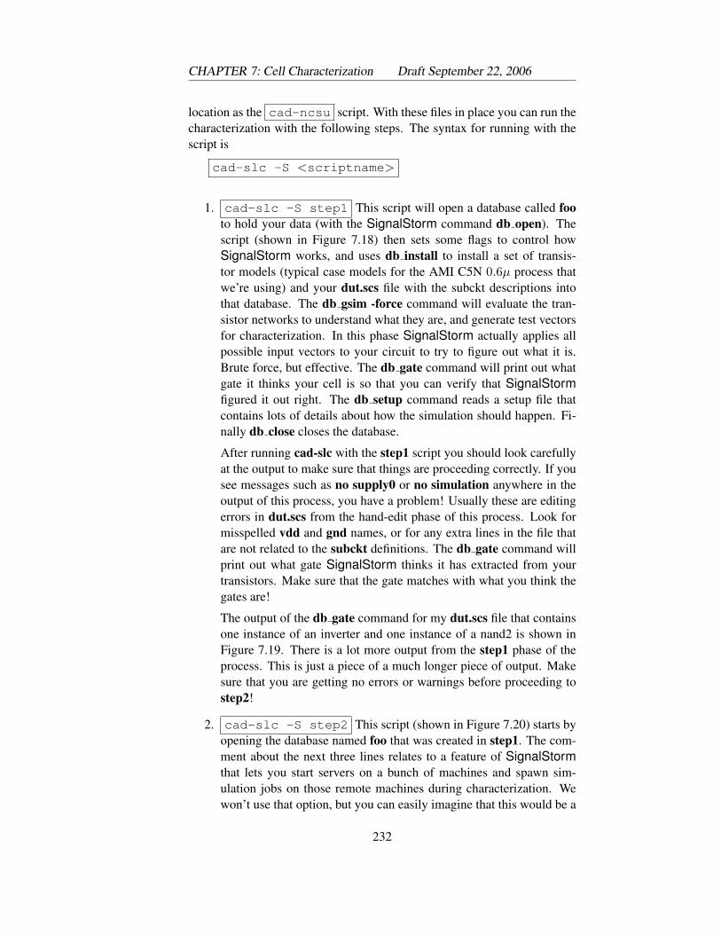
CHAPTER 7: Cell Characterization Draft September 22, 2006
location as the cad-ncsu script. With these files in place you can run thecharacterization with the following steps. The syntax for running with thescript is
cad-slc -S <scriptname>
1. cad-slc -S step1 This script will open a database called footo hold your data (with the SignalStorm command db open). Thescript (shown in Figure 7.18) then sets some flags to control howSignalStorm works, and uses db install to install a set of transis-tor models (typical case models for the AMI C5N 0.6µ process thatwe’re using) and your dut.scs file with the subckt descriptions intothat database. The db gsim -force command will evaluate the tran-sistor networks to understand what they are, and generate test vectorsfor characterization. In this phase SignalStorm actually applies allpossible input vectors to your circuit to try to figure out what it is.Brute force, but effective. The db gate command will print out whatgate it thinks your cell is so that you can verify that SignalStormfigured it out right. The db setup command reads a setup file thatcontains lots of details about how the simulation should happen. Fi-nally db close closes the database.
After running cad-slc with the step1 script you should look carefullyat the output to make sure that things are proceeding correctly. If yousee messages such as no supply0 or no simulation anywhere in theoutput of this process, you have a problem! Usually these are editingerrors in dut.scs from the hand-edit phase of this process. Look formisspelled vdd and gnd names, or for any extra lines in the file thatare not related to the subckt definitions. The db gate command willprint out what gate SignalStorm thinks it has extracted from yourtransistors. Make sure that the gate matches with what you think thegates are!
The output of the db gate command for my dut.scs file that containsone instance of an inverter and one instance of a nand2 is shown inFigure 7.19. There is a lot more output from the step1 phase of theprocess. This is just a piece of a much longer piece of output. Makesure that you are getting no errors or warnings before proceeding tostep2!
2. cad-slc -S step2 This script (shown in Figure 7.20) starts byopening the database named foo that was created in step1. The com-ment about the next three lines relates to a feature of SignalStormthat lets you start servers on a bunch of machines and spawn sim-ulation jobs on those remote machines during characterization. Wewon’t use that option, but you can easily imagine that this would be a
232
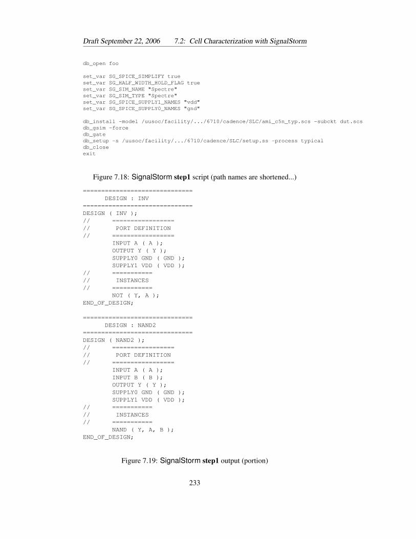
Draft September 22, 2006 7.2: Cell Characterization with SignalStorm
db_open foo
set_var SG_SPICE_SIMPLIFY trueset_var SG_HALF_WIDTH_HOLD_FLAG trueset_var SG_SIM_NAME "Spectre"set_var SG_SIM_TYPE "Spectre"set_var SG_SPICE_SUPPLY1_NAMES "vdd"set_var SG_SPICE_SUPPLY0_NAMES "gnd"
db_install -model /uusoc/facility/.../6710/cadence/SLC/ami_c5n_typ.scs -subckt dut.scsdb_gsim -forcedb_gatedb_setup -s /uusoc/facility/.../6710/cadence/SLC/setup.ss -process typicaldb_closeexit
Figure 7.18: SignalStorm step1 script (path names are shortened...)
==============================DESIGN : INV
==============================DESIGN ( INV );// =================// PORT DEFINITION// =================
INPUT A ( A );OUTPUT Y ( Y );SUPPLY0 GND ( GND );SUPPLY1 VDD ( VDD );
// ===========// INSTANCES// ===========
NOT ( Y, A );END_OF_DESIGN;
==============================DESIGN : NAND2
==============================DESIGN ( NAND2 );// =================// PORT DEFINITION// =================
INPUT A ( A );INPUT B ( B );OUTPUT Y ( Y );SUPPLY0 GND ( GND );SUPPLY1 VDD ( VDD );
// ===========// INSTANCES// ===========
NAND ( Y, A, B );END_OF_DESIGN;
Figure 7.19: SignalStorm step1 output (portion)
233
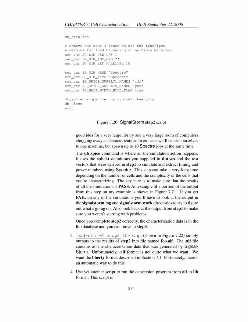
CHAPTER 7: Cell Characterization Draft September 22, 2006
db_open foo
# Remove the next 3 lines to use the ipsd/ipsc# deamons for load balancing on multiple machinesset_var SG_SIM_USE_LSF 1set_var SG_SIM_LSF_CMD ""set_var SG_SIM_LSF_PARALLEL 10
set_var SG_SIM_NAME "Spectre"set_var SG_SIM_TYPE "Spectre"set_var SG_SPICE_SUPPLY1_NAMES "vdd"set_var SG_SPICE_SUPPLY0_NAMES "gnd"set_var SG_HALF_WIDTH_HOLD_FLAG true
db_spice -s spectre -p typical -keep_logdb_closeexit
Figure 7.20: SignalStorm step2 script
good idea for a very large library and a very large room of computerschugging away at characterization. In our case we’ll restrict ourselvesto one machine, but spawn up to 10 Spectre jobs at the same time.
The db spice command is where all the simulation action happens.It uses the subckt definitions you supplied in dut.scs and the testvectors that were derived in step1 to simulate and extract timing andpower numbers using Spectre. This step can take a very long timedepending on the number of cells and the complexity of the cells thatyou’re characterizing. The key here is to make sure that the resultsof all the simulations is PASS. An example of a portion of the outputfrom this step on my example is shown in Figure 7.21. If you getFAIL on any of the simulations you’ll have to look at the output inthe signalstorm.log and signalstorm.work directories to try to figureout what’s going on. Also look back at the output from step1 to makesure you weren’t starting with problems.
Once you complete step2 correctly, the characterization data is in thefoo database and you can move to step3.
3. cad-slc -S step3 This script (shown in Figure 7.22) simplyoutputs to the results of step2 into file named foo.alf. The .alf filecontains all the characerization data that was generated by Signal-Storm. Unfortunately, .alf format is not quite what we want. Wewant the liberty format described in Section 7.1. Fortunately, there’san automatic way to do this.
4. Use yet another script to run the conversion program from alf to libformat. This script is
234
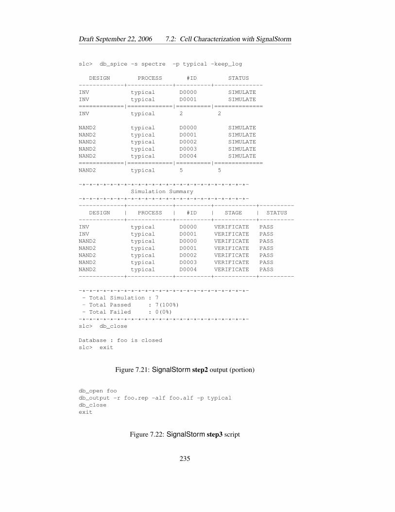
Draft September 22, 2006 7.2: Cell Characterization with SignalStorm
slc> db_spice -s spectre -p typical -keep_log
DESIGN PROCESS #ID STATUS-------------+-------------+----------+--------------INV typical D0000 SIMULATEINV typical D0001 SIMULATE=============|=============|==========|==============INV typical 2 2
NAND2 typical D0000 SIMULATENAND2 typical D0001 SIMULATENAND2 typical D0002 SIMULATENAND2 typical D0003 SIMULATENAND2 typical D0004 SIMULATE=============|=============|==========|==============NAND2 typical 5 5
-*-*-*-*-*-*-*-*-*-*-*-*-*-*-*-*-*-*-*-*-*-*-*-*-Simulation Summary
-*-*-*-*-*-*-*-*-*-*-*-*-*-*-*-*-*-*-*-*-*-*-*-*--------------+-------------+----------+------------+----------
DESIGN | PROCESS | #ID | STAGE | STATUS-------------+-------------+----------+------------+----------INV typical D0000 VERIFICATE PASSINV typical D0001 VERIFICATE PASSNAND2 typical D0000 VERIFICATE PASSNAND2 typical D0001 VERIFICATE PASSNAND2 typical D0002 VERIFICATE PASSNAND2 typical D0003 VERIFICATE PASSNAND2 typical D0004 VERIFICATE PASS-------------+-------------+----------+------------+----------
-*-*-*-*-*-*-*-*-*-*-*-*-*-*-*-*-*-*-*-*-*-*-*-*-- Total Simulation : 7- Total Passed : 7(100%)- Total Failed : 0(0%)-*-*-*-*-*-*-*-*-*-*-*-*-*-*-*-*-*-*-*-*-*-*-*-*-slc> db_close
Database : foo is closedslc> exit
Figure 7.21: SignalStorm step2 output (portion)
db_open foodb_output -r foo.rep -alf foo.alf -p typicaldb_closeexit
Figure 7.22: SignalStorm step3 script
235
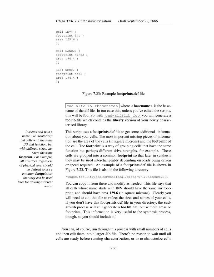
CHAPTER 7: Cell Characterization Draft September 22, 2006
cell INV* {footprint inv ;area 129.6 ;};
cell NAND2* {footprint nand2 ;area 194.4 ;};
cell NOR2* {footprint nor2 ;area 194.4 ;};
Figure 7.23: Example footprints.def file
cad-alf2lib <basename> where <basename> is the base-name of the alf file. In our case this, unless you’ve edited the scripts,this will be foo. So, with cad-alf2lib foo you will generate afoo.lib file which contains the liberty version of your newly charac-terized library.
This script uses a footprints.def file to get some additional informa-It seems odd with aname like “footprint,”
but cells with the sameI/O and function, but
with different sizes, canshare the same
footprint. For example,all inverters, regardless
of physical area, shouldbe defined to use a
common footprint sothat they can be used
later for driving differentloads.
tion about your cells. The most important missing pieces of informa-tion are the area of the cells (in square microns) and the footprint ofthe cell. The footprint is a way of grouping cells that have the samefunction but perhaps different drive strengths, for example. Thesecells are grouped into a common footprint so that later in synthesisthey may be used interchangeably depending on loads being drivenor speed required. An example of a footprints.def file is shown inFigure 7.23. This file is also in the following directory:
/uusoc/facility/cad common/local/class/6710/cadence/SLC
You can copy it from there and modify as needed. This file says thatall cells whose name starts with INV should have the same inv foot-print, and should have area 129.6 (in square microns). Clearly youwill need to edit this file to reflect the sizes and names of your cells.If you don’t have this footprints.def file in your directory, the cad-alf2lib process will still generate a foo.lib file, but without areas orfootprints. This information is very useful to the synthesis process,though, so you should include it!
You can, of course, run through this process with small numbers of cellsand then edit them into a larger .lib file. There’s no reason to wait until allcells are ready before running characterization, or to re-characterize cells
236
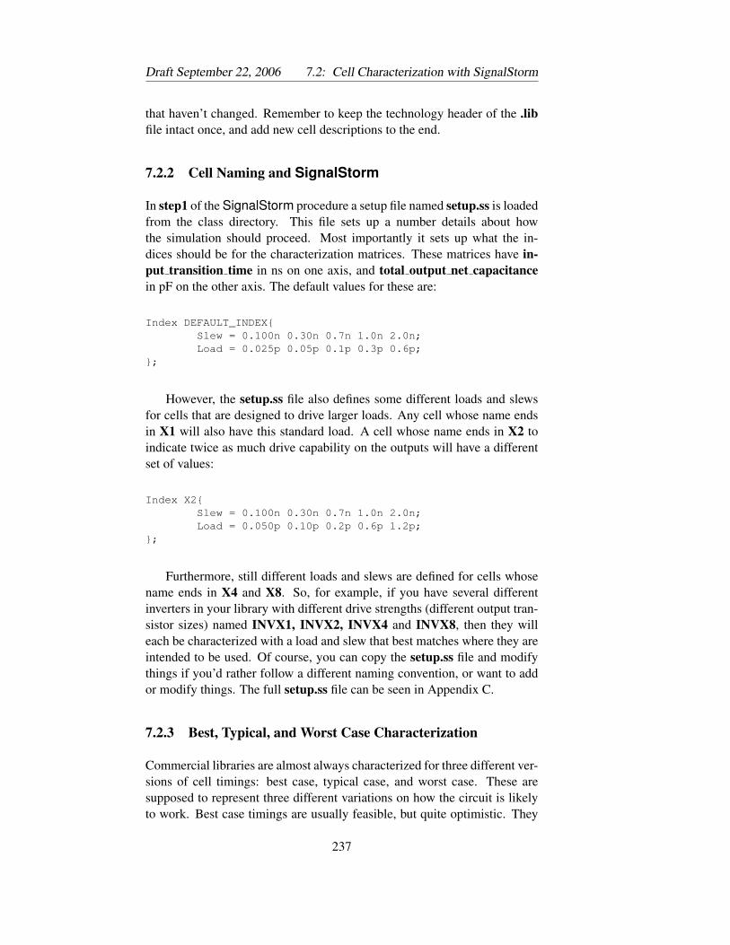
Draft September 22, 2006 7.2: Cell Characterization with SignalStorm
that haven’t changed. Remember to keep the technology header of the .libfile intact once, and add new cell descriptions to the end.
7.2.2 Cell Naming and SignalStorm
In step1 of the SignalStorm procedure a setup file named setup.ss is loadedfrom the class directory. This file sets up a number details about howthe simulation should proceed. Most importantly it sets up what the in-dices should be for the characterization matrices. These matrices have in-put transition time in ns on one axis, and total output net capacitancein pF on the other axis. The default values for these are:
Index DEFAULT_INDEX{Slew = 0.100n 0.30n 0.7n 1.0n 2.0n;Load = 0.025p 0.05p 0.1p 0.3p 0.6p;
};
However, the setup.ss file also defines some different loads and slewsfor cells that are designed to drive larger loads. Any cell whose name endsin X1 will also have this standard load. A cell whose name ends in X2 toindicate twice as much drive capability on the outputs will have a differentset of values:
Index X2{Slew = 0.100n 0.30n 0.7n 1.0n 2.0n;Load = 0.050p 0.10p 0.2p 0.6p 1.2p;
};
Furthermore, still different loads and slews are defined for cells whosename ends in X4 and X8. So, for example, if you have several differentinverters in your library with different drive strengths (different output tran-sistor sizes) named INVX1, INVX2, INVX4 and INVX8, then they willeach be characterized with a load and slew that best matches where they areintended to be used. Of course, you can copy the setup.ss file and modifythings if you’d rather follow a different naming convention, or want to addor modify things. The full setup.ss file can be seen in Appendix C.
7.2.3 Best, Typical, and Worst Case Characterization
Commercial libraries are almost always characterized for three different ver-sions of cell timings: best case, typical case, and worst case. These aresupposed to represent three different variations on how the circuit is likelyto work. Best case timings are usually feasible, but quite optimistic. They
237
CHAPTER 7: Cell Characterization Draft September 22, 2006
assume transistors that operate in the fast region measured by the foundry,with a vdd that’s typically 10% higher than nominal, and at a nice cool tem-perature. Typical case timings are supposed to model what you’ll usuallysee in the fabricated circuit. The transistor models are taken from the mid-dle of the measured performance distribution, vdd is nominal (5v in our 6µprocess), and the temperature is assumed to be 25C. Worst case timings aretaken from the slow end of the transistor distribution, with vdd at 10% belownominal, and a nice toasty temperature of 125C. If you’re trying to see whatspeed your circuit might run at, use the typical timings. If you’re trying tosee whether your circuit will work in more general environments, use theworst timings. Only a very optimistic person would ever use best timings!
The step1, step2 and step3 scripts are designed to measure typical casetimings for you cells. However, if you would like to generate best and worstcase libraries as well, there are versions of the scripts to do this. For ex-ample, step[1,2,3] worst will measure wort case timings using worst-casetransistor models from MOSIS, vdd assumed to be 4.5v, and a temperatureof 125C. These scripts are in the class library.
7.3 Characterization with Spectre
If you want to characterize cells by hand, you can do this using SpectreSby making your own test fixture circuits and doing analog simulation asdescribed in Chapter 6. This is clearly a little more hand-work than lettingSignalStorm run everything, but you have much more control over everyaspect of the characterizations. My recommendation is to use SignalStorm,but here are some things to think about if you’d like to do things directly withSpectreS.
The process of characterizing cells involves running lots of simulationwhile varying the input slope and the output load so that you can fill out thetiming tables. This argues strongly for using parametric simulation whereyou vary the parameters of the voltage sources and the output loads auto-matically. For example, you could set up a test fixture schematic as in Fig-ure 7.24. In this test fixture the DUT is driven by a vpulse voltage source,and is driving load capacitor. The slope of the pulse will be controlled by avariable named slope and the size of the load will be controlled by a vari-able named load. To assign these component parameters a variable name,simply give the variable name in the q properties of the device instead ofa numeric value.
Now you can use the same parametric simulation techniques as de-scribed in Chapter 6 Section 6.4.1. In this case you could vary the inputslope to be a series of times in ns, and the output load to be a series of val-
238
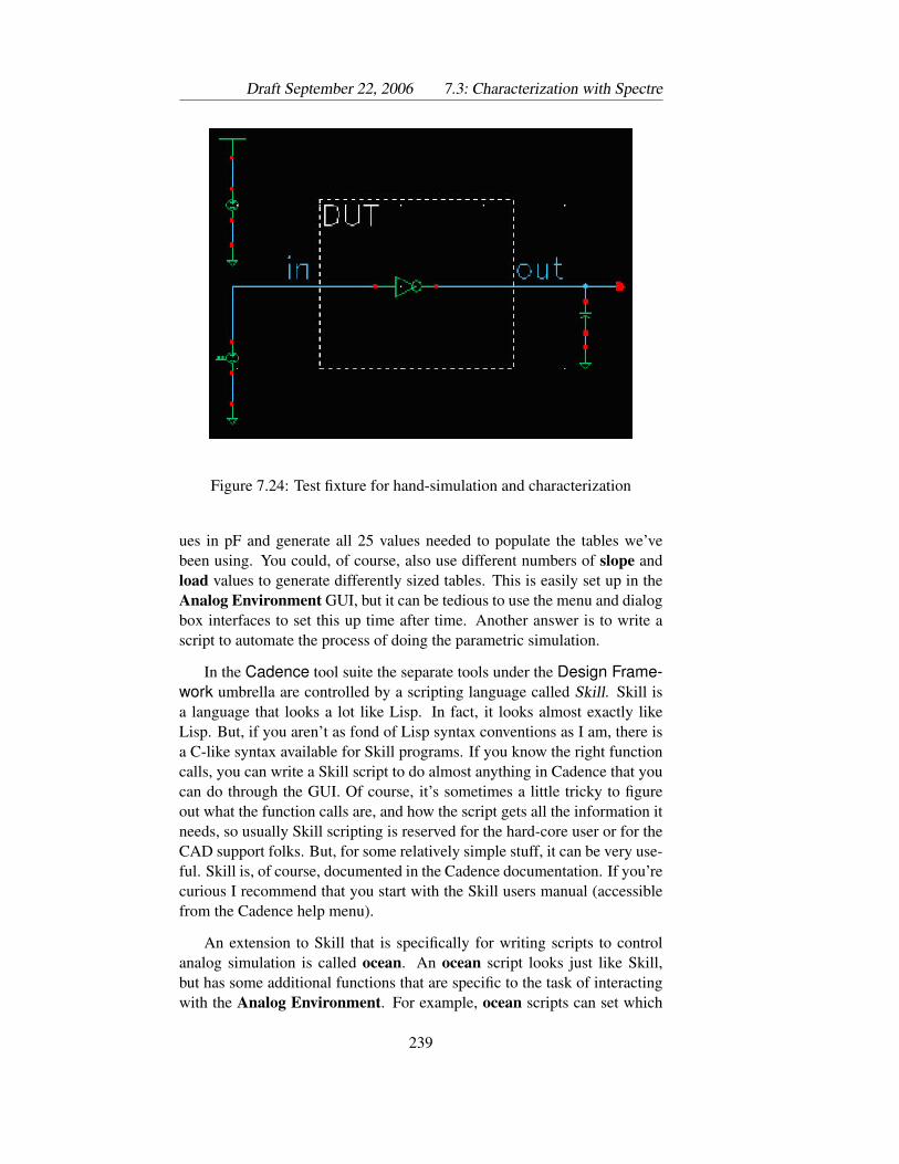
Draft September 22, 2006 7.3: Characterization with Spectre
Figure 7.24: Test fixture for hand-simulation and characterization
ues in pF and generate all 25 values needed to populate the tables we’vebeen using. You could, of course, also use different numbers of slope andload values to generate differently sized tables. This is easily set up in theAnalog Environment GUI, but it can be tedious to use the menu and dialogbox interfaces to set this up time after time. Another answer is to write ascript to automate the process of doing the parametric simulation.
In the Cadence tool suite the separate tools under the Design Frame-work umbrella are controlled by a scripting language called Skill. Skill isa language that looks a lot like Lisp. In fact, it looks almost exactly likeLisp. But, if you aren’t as fond of Lisp syntax conventions as I am, there isa C-like syntax available for Skill programs. If you know the right functioncalls, you can write a Skill script to do almost anything in Cadence that youcan do through the GUI. Of course, it’s sometimes a little tricky to figureout what the function calls are, and how the script gets all the information itneeds, so usually Skill scripting is reserved for the hard-core user or for theCAD support folks. But, for some relatively simple stuff, it can be very use-ful. Skill is, of course, documented in the Cadence documentation. If you’recurious I recommend that you start with the Skill users manual (accessiblefrom the Cadence help menu).
An extension to Skill that is specifically for writing scripts to controlanalog simulation is called ocean. An ocean script looks just like Skill,but has some additional functions that are specific to the task of interactingwith the Analog Environment. For example, ocean scripts can set which
239
CHAPTER 7: Cell Characterization Draft September 22, 2006
design you’re looking at, which set of waveform results you’re evaluating,and which signals in those waveforms you’re measuring.
I’ve written an ocean script that you can use or modify to perform para-metric simulation of a cell and which will generate the output in a set oflookup tables formatted for the .lib file. It turns out that formatting the out-put to look like liberty format wants it is practically the hardest part! Theother hard part is that I can’t figure out is how to generate the netlist forsimulation in the first place in the script, so you still need to use the AnalogEnvironment GUI for part of the process, the same as for SignalStorm.But, after you get things set up, it’s as easy as typing a function name in theCIW and you get the parametric simulation results generated for you. Ofcourse, it’s not remotely as automated as SignalStorm so I still recommendthat you stop reading now and go back to the SignalStorm section!
If you’re still reading, in order to use the script, you’ll need a schematicthat describes the DUT simulation setup. I called this schematic test setupfor lack of a more imaginative name. Because we’re aiming to simulateover a range of output loads I put a capacitor on the output with the variableload as the capacitance value. Because we’re also aiming to simulate overa range of input slopes, I put a Vpulse on the input of the DUT with thevariable slope as the rise and fall time values. I can then use the parametricsimulation setup to vary both of those values. The schematic is shown inFigure 7.24.
Notice that the DUT is being driven by the Vpulse and is driving intothe load capacitor. If you were simulating a multi-input gate, you’d needto tie the non-driven inputs of that gate to an appropriate value that wouldturn the output of the gate to either an inverter or a buffer. For example, ifyou were simulating a 2-input NAND gate, you’d want to tie the input thatyou’re not driving to logic 1 (vdd) so that the pulse on the other input wouldcome through the output as an inverted signal. Remember that you need togenerate timing for all outputs with respect to all inputs so in the case of a2-input NAND you’d need timing from A→ Y and from B→ Y. Each timeyou would modify the schematic and generate a new netlist to simulate withthe script. You also need to keep track of whether the gate is acting like aninverter (negative unate timing), or as a buffer (positive unate timing) forthis simulation.
In order to make sure that I’m simulating the right thing, I’ll need aconfig view of the test setup schematic, just like you’ve done before. In theconfig view you will want to specify the analog extracted view of whatevercell you’re using as the DUT in this simulation run. In Figure 7.25 you cansee the config view of my test setup schematic with the analog extractedview of my inverter selected.
To generate the analog netlist open the test setup schematic and then
240
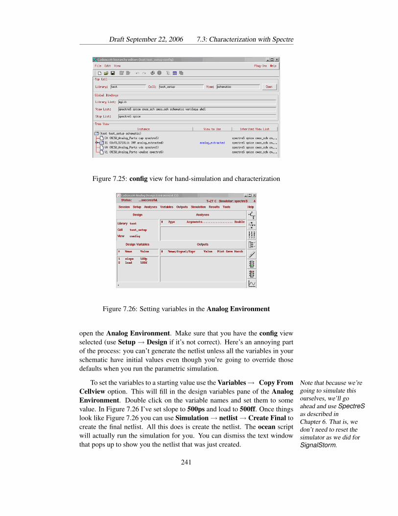
Draft September 22, 2006 7.3: Characterization with Spectre
Figure 7.25: config view for hand-simulation and characterization
Figure 7.26: Setting variables in the Analog Environment
open the Analog Environment. Make sure that you have the config viewselected (use Setup → Design if it’s not correct). Here’s an annoying partof the process: you can’t generate the netlist unless all the variables in yourschematic have initial values even though you’re going to override thosedefaults when you run the parametric simulation.
To set the variables to a starting value use the Variables→ Copy From Note that because we’regoing to simulate thisourselves, we’ll goahead and use SpectreSas described inChapter 6. That is, wedon’t need to reset thesimulator as we did forSignalStorm.
Cellview option. This will fill in the design variables pane of the AnalogEnvironment. Double click on the variable names and set them to somevalue. In Figure 7.26 I’ve set slope to 500ps and load to 500ff. Once thingslook like Figure 7.26 you can use Simulation → netlist → Create Final tocreate the final netlist. All this does is create the netlist. The ocean scriptwill actually run the simulation for you. You can dismiss the text windowthat pops up to show you the netlist that was just created.
241
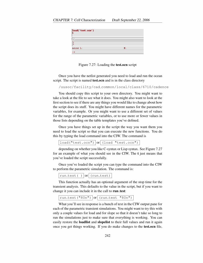
CHAPTER 7: Cell Characterization Draft September 22, 2006
Figure 7.27: Loading the test.ocn script
Once you have the netlist generated you need to load and run the oceanscript. The script is named test.ocn and is in the class directory
/uusoc/facility/cad common/local/class/6710/cadence
You should copy this script to your own directory. You might want totake a look at the file to see what it does. You might also want to look at thefirst section to see if there are any things you would like to change about howthe script does its stuff. You might have different names for the parametricvariables, for example. Or you might want to use a different set of valuesfor the range of the parametric variables, or to use more or fewer values inthose lists depending on the table templates you’ve defined.
Once you have things set up in the script the way you want them youneed to load the script so that you can execute the new functions. You dothis by typing the load command into the CIW. The command is
load("test.ocn") or (load "test.ocn")
depending on whether you like C-syntax or Lisp syntax. See Figure 7.27for an example of what you should see in the CIW. The t just means thatyou’ve loaded the script successfully.
Once you’ve loaded the script you can type the command into the CIWto perform the parametric simulation. The command is:
run test( ) or (run test)
This function actually has an optional argument of the stop time for thetransient analysis. This defaults to the value in the script, but if you want tochange it you can include it in the call to run test:
run test("80n") or (run test "80n")
What you’ll see in response is a bunch of text in the CIW output pane foreach of the parametric transient simulations. You might want to try this withonly a couple values for load and for slope so that it doesn’t take so long torun the simulations just to make sure that everything is working. You caneasily restore the loadlist and slopelist to their full values and run it againonce you get things working. If you do make changes to the test.ocn file,
242
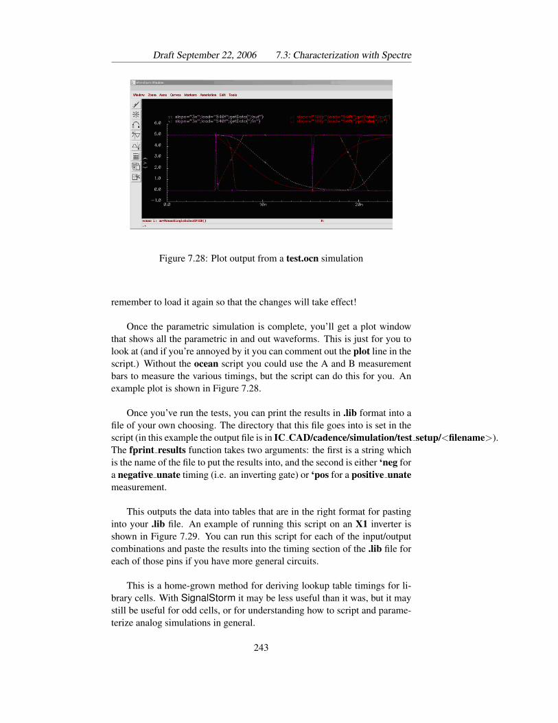
Draft September 22, 2006 7.3: Characterization with Spectre
Figure 7.28: Plot output from a test.ocn simulation
remember to load it again so that the changes will take effect!
Once the parametric simulation is complete, you’ll get a plot windowthat shows all the parametric in and out waveforms. This is just for you tolook at (and if you’re annoyed by it you can comment out the plot line in thescript.) Without the ocean script you could use the A and B measurementbars to measure the various timings, but the script can do this for you. Anexample plot is shown in Figure 7.28.
Once you’ve run the tests, you can print the results in .lib format into afile of your own choosing. The directory that this file goes into is set in thescript (in this example the output file is in IC CAD/cadence/simulation/test setup/<filename>).The fprint results function takes two arguments: the first is a string whichis the name of the file to put the results into, and the second is either ‘neg fora negative unate timing (i.e. an inverting gate) or ‘pos for a positive unatemeasurement.
This outputs the data into tables that are in the right format for pastinginto your .lib file. An example of running this script on an X1 inverter isshown in Figure 7.29. You can run this script for each of the input/outputcombinations and paste the results into the timing section of the .lib file foreach of those pins if you have more general circuits.
This is a home-grown method for deriving lookup table timings for li-brary cells. With SignalStorm it may be less useful than it was, but it maystill be useful for odd cells, or for understanding how to script and parame-terize analog simulations in general.
243
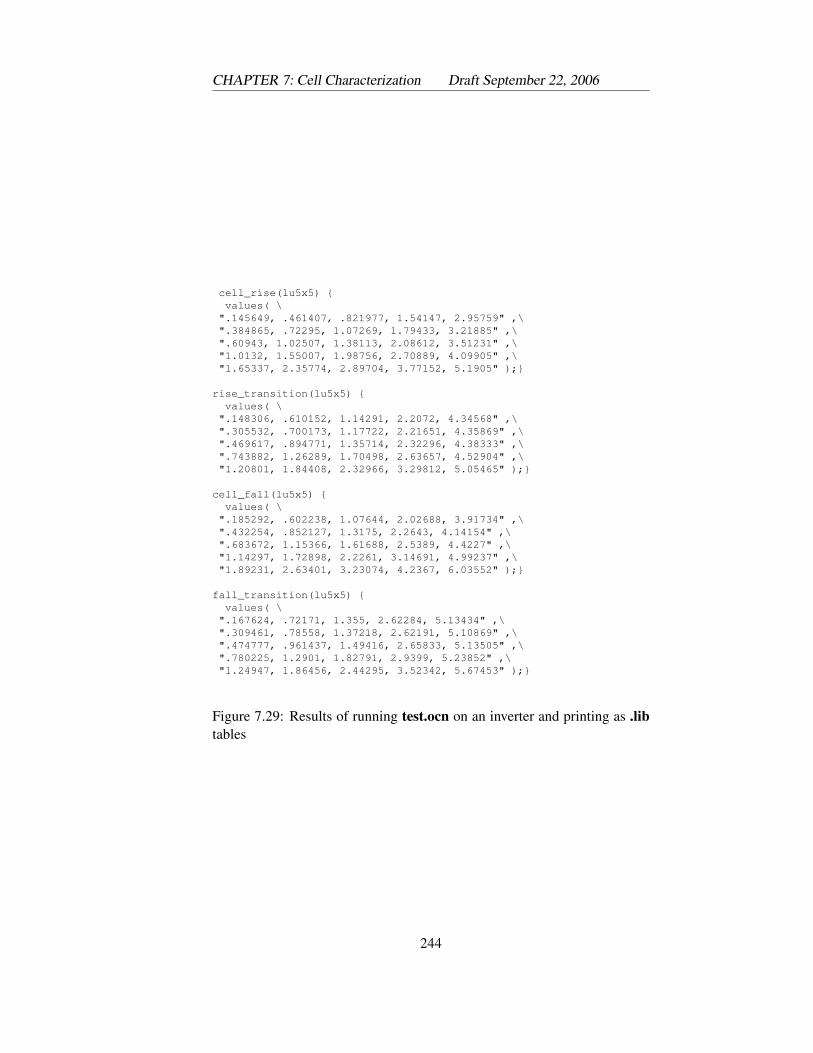
CHAPTER 7: Cell Characterization Draft September 22, 2006
cell_rise(lu5x5) {values( \
".145649, .461407, .821977, 1.54147, 2.95759" ,\".384865, .72295, 1.07269, 1.79433, 3.21885" ,\".60943, 1.02507, 1.38113, 2.08612, 3.51231" ,\"1.0132, 1.55007, 1.98756, 2.70889, 4.09905" ,\"1.65337, 2.35774, 2.89704, 3.77152, 5.1905" );}
rise_transition(lu5x5) {values( \
".148306, .610152, 1.14291, 2.2072, 4.34568" ,\".305532, .700173, 1.17722, 2.21651, 4.35869" ,\".469617, .894771, 1.35714, 2.32296, 4.38333" ,\".743882, 1.26289, 1.70498, 2.63657, 4.52904" ,\"1.20801, 1.84408, 2.32966, 3.29812, 5.05465" );}
cell_fall(lu5x5) {values( \
".185292, .602238, 1.07644, 2.02688, 3.91734" ,\".432254, .852127, 1.3175, 2.2643, 4.14154" ,\".683672, 1.15366, 1.61688, 2.5389, 4.4227" ,\"1.14297, 1.72898, 2.2261, 3.14691, 4.99237" ,\"1.89231, 2.63401, 3.23074, 4.2367, 6.03552" );}
fall_transition(lu5x5) {values( \
".167624, .72171, 1.355, 2.62284, 5.13434" ,\".309461, .78558, 1.37218, 2.62191, 5.10869" ,\".474777, .961437, 1.49416, 2.65833, 5.13505" ,\".780225, 1.2901, 1.82791, 2.9399, 5.23852" ,\"1.24947, 1.86456, 2.44295, 3.52342, 5.67453" );}
Figure 7.29: Results of running test.ocn on an inverter and printing as .libtables
244
Draft September 22, 2006 7.4: Converting Liberty to SynopsysDatabase Format
7.4 Converting Liberty to Synopsys Database For-mat
Once you have generated a liberty formatted file that describes your cellsyou should be done because this is the most common industry standard for-mat for describing cell timing and power data. But, even though this is aformat that originally came from Synopsys, the Synopsys tools actuallyrequire a compiled format that is compiled from this liberty text descrip-tion. The Synopsys library compiler tool can easily compile the .lib fileinto this .db format, but unfortunately, and for reasons I don’t understand,the .lib file that is generated by SignalStorm actually needs a little hand-modification to be completely compatable with Synopsys! Annoying buttrue.
Start with the .lib file that you got from SignalStorm and make thefollowing changes. If you’ve written your own .lib file then you may haveother issues of course, but you also need to pay attention to these.
• There are errors in the compilation process if a pin has a a fall capacitance rangeparameter, but not a rise capacitance range. One quick fix is just totake out all [rise/fall] capacitance range lines. This won’t cause ahuge difference. These lines describe the range of capacitance a pinwill see during signal transitions. Alternatively, you could add the Instructions for
compiling .lib into .dbare coming up in thissection
missing [rise/fall] capacitance range statement for each pin that hasone but not the other. For the missing range you can use the singlevalue for the pin capacitance for the top and bottom of the range.
• If you remove all those attributes, you may get warnings about nothaving them, but you can ignore them. Look at the warnings. Theytell you that the compiler will assume that the range is just equal tothe one measured value, which should be fine.
• If you have negative delays in any of your timing tables (I had themfor disable timings for the eninv when the input rise times were slow,for example) you should “round” those negative timings to 0.
• If you want to avoid warinings about not having default values set youshould include the following lines in the technology header section ofyour .lib file:
/* Default attributes */
/* Fanout (in terms of capacitive load units) */default_fanout_load : 0.3 ;
245
CHAPTER 7: Cell Characterization Draft September 22, 2006
default_max_fanout : 10.0 ;
/* Pin Capacitance */default_inout_pin_cap : 0.00675 ;default_input_pin_cap : 0.00675 ;default_output_pin_cap : 0.0 ;
/* leakage power */default_cell_leakage_power : 0.0 ;default_leakage_power_density : 0.0 ;
• If you want to include the wire load models, include the text fromFigures 7.3 and 7.4 in the tech header section of your .lib file.
Once you have a correct (and correctly modified) .lib file you can com-pile it into a Synopsys synthesis database (.db) file. To do this you needto run the Synopsys design compiler synthesis tool, but only in a verysimple way. The command to start design compiler or, more precicely thecommand-line shell version called dc shell is with the command
syn-dc
This will start up design compiler in a mode where you can type incommands to the design compiler shell. What you want to do is read inthe library in .lib format, and write out that library in .db format. The firstcommand that you type to the shell is the read lib command to read the.lib file. It looks like (dc shell-xg-t> is the design compiler shell prompt:
dc shell-xg-t> read lib <filename>.lib
where, of course, <filename>.lib is the name of your .lib file. This willissue a bunch of warnings about defining new variables and perhaps aboutmissing range attributes. You should look carefully at this stage to makesure there are no errors! If you are satisfied that there are only warnings andthat the warnings are not important, you can then write out that library in.db format with the write lib command. THe name of the library isthe name you defined in the library(<name>) command at the top of your.lib file.
dc shell-xg-t> write lib <libname> -o <libname>.db
The -o switch lets you specify whatever file name you like for the outputfile, but your life will be easier if you name it with a .db extension.
If this finishes without error, you can exit with the exit command tothe design compiler shell. You now (hopefully) have a correctly formatedbinary database for your cell library that Synopsys can use in its synthesisprocedure.
246
Chapter 8
Verilog Synthesis
SYNTHESIS is the process of taking a behavioral Verilog file and con-verting it to a structural file using cells from a standard cell library.That is, the behavior that is captured by the Verilog program is syn-
thesized into a circuit that behaves in the same way. The synthesized circuitis described as a collection of cells from the target cell library. This Verilogfile is known as structural because it is strictly structural instantiations ofcells. It is the Verilog text equivalent of a schematic. This structural file canbe used as the starting point for the backend tools which will place thosecells on the chip and route the wire connections between them.
There are three different behavioral synthesis tools that are usable in ourflow, and one schematic-based helper application. They are:
Synopsys Design Compiler: This is the flagship synthesis tool from TCL is Tool CommandLanguage and is astandard syntax forproviding inputcommands to tools.
Synopsys. It comes in two flavors: dc shell which has a TCL shell-command interface and design vision which is a gui window/menudriven version. The dc shell version is often driven by writing scriptsand executing those scripts on new designs.
Synopsys Module Compiler: This is a specialty synthesis tool from Syn-opsys that is specifically for synthesis of arithmetic circuits. It hasmore knowledge of different arithmetic circuit variants than designcompiler, including many fast adder variants and even floating pointmodels. It also has its own circuit specification language that you canuse to describe complex arithmetic operations. It uses the same targetlibrary database at design compiler.
Cadence Build Gates: This is the primary synthesis tool from Cadence.It uses the .lib file directly as the cell database and it is also usuallydriven from scripts.
CHAPTER 8: Verilog Synthesis Draft September 25, 2006
Cadence to Synopsys Interface (CSI): This is a tool integrated withthe Composer schematic capture tool that lets you take schemat-ics that use a combination of standard cells and behavioral Verilog(wrapped in Composer symbols) and output that schematic as a struc-tural Verilog file.
8.1 Synopsys Synthesis: Basic Synthesis
In order to make use of Synopsys synthesis you need (at least) the follow-ing files:
.synopsys dc.setup: This is the setup file for design compiler and modulecompiler. It can be copied from
/uusoc/facility/cad common/local/class/6710/synopsys
Note that it has a dot as the first character in the file name. You shouldcopy this file into the directory from which you plan to run the Syn-opsys tools.
a cell database file: This is the binary .db file that contains the cell infor-mation for the target library that you would like your behavior com-piled to. Details of cell characterization and file formats for charac-terized libraries are in Chapter 7. It’s helpful if you either have thisfile in the directory from which you are running Synopsys, or makea link to it in that directory if it really lives elsewhere.
A behavioral Verilog file: This is the file whose behavior you would liketo synthesize into a circuit. It can contain purely behavioral code, ora mixture of behavioral and structural (cell instantiations) code. Thisshould also be either in or linked to the directory you use for runningSynopsys
If you have these three files you can run very basic synthesis using aclass script. This script, named beh2str , converts a behavioral Verilogfile into a structural Verilog file in a very simplified way. It does no fancyoptimization, and it only works for a single behavioral Verilog file as input(no multiple-file designs). It’s not really designed for final synthesis, it’sjust deigned as a quick and dirty script that you can use to check and seehow things are working, and for initial investigations into small designs. Touse the script you don’t need to know anything about what design compileris actually doing. For more advanced synthesis you’ll want much moredirect control. But, this is a good introduction to the process of synthesis,and a good way to see what the synthesis engine does to different ways ofexpressing things in Verilog.
248
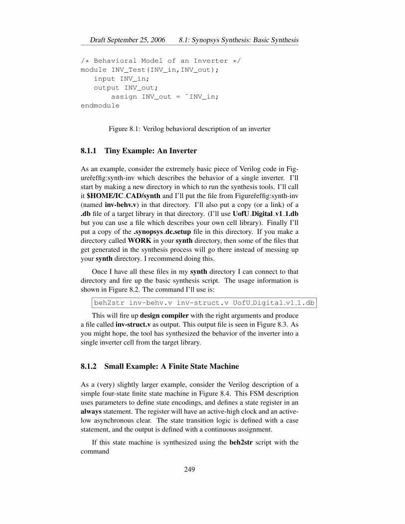
Draft September 25, 2006 8.1: Synopsys Synthesis: Basic Synthesis
/* Behavioral Model of an Inverter */module INV_Test(INV_in,INV_out);
input INV_in;output INV_out;
assign INV_out = ˜INV_in;endmodule
Figure 8.1: Verilog behavioral description of an inverter
8.1.1 Tiny Example: An Inverter
As an example, consider the extremely basic piece of Verilog code in Fig-urereffig:synth-inv which describes the behavior of a single inverter. I’llstart by making a new directory in which to run the synthesis tools. I’ll callit $HOME/IC CAD/synth and I’ll put the file from Figurereffig:synth-inv(named inv-behv.v) in that directory. I’ll also put a copy (or a link) of a.db file of a target library in that directory. (I’ll use UofU Digital v1 1.dbbut you can use a file which describes your own cell library). Finally I’llput a copy of the .synopsys dc.setup file in this directory. If you make adirectory called WORK in your synth directory, then some of the files thatget generated in the synthesis process will go there instead of messing upyour synth directory. I recommend doing this.
Once I have all these files in my synth directory I can connect to thatdirectory and fire up the basic synthesis script. The usage information isshown in Figure 8.2. The command I’ll use is:
beh2str inv-behv.v inv-struct.v UofU Digital v1 1.db
This will fire up design compiler with the right arguments and producea file called inv-struct.v as output. This output file is seen in Figure 8.3. Asyou might hope, the tool has synthesized the behavior of the inverter into asingle inverter cell from the target library.
8.1.2 Small Example: A Finite State Machine
As a (very) slightly larger example, consider the Verilog description of asimple four-state finite state machine in Figure 8.4. This FSM descriptionuses parameters to define state encodings, and defines a state register in analways statement. The register will have an active-high clock and an active-low asynchronous clear. The state transition logic is defined with a casestatement, and the output is defined with a continuous assignment.
If this state machine is synthesized using the beh2str script with thecommand
249
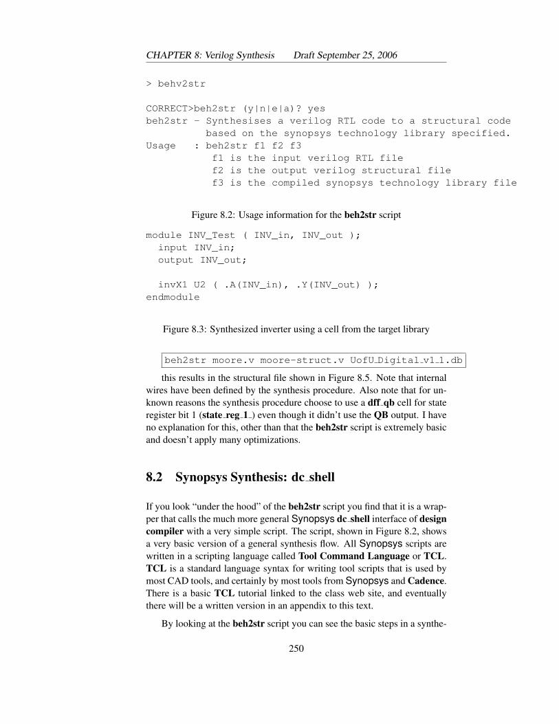
CHAPTER 8: Verilog Synthesis Draft September 25, 2006
> behv2str
CORRECT>beh2str (y|n|e|a)? yesbeh2str - Synthesises a verilog RTL code to a structural code
based on the synopsys technology library specified.Usage : beh2str f1 f2 f3
f1 is the input verilog RTL filef2 is the output verilog structural filef3 is the compiled synopsys technology library file
Figure 8.2: Usage information for the beh2str script
module INV_Test ( INV_in, INV_out );input INV_in;output INV_out;
invX1 U2 ( .A(INV_in), .Y(INV_out) );endmodule
Figure 8.3: Synthesized inverter using a cell from the target library
beh2str moore.v moore-struct.v UofU Digital v1 1.db
this results in the structural file shown in Figure 8.5. Note that internalwires have been defined by the synthesis procedure. Also note that for un-known reasons the synthesis procedure choose to use a dff qb cell for stateregister bit 1 (state reg 1 ) even though it didn’t use the QB output. I haveno explanation for this, other than that the beh2str script is extremely basicand doesn’t apply many optimizations.
8.2 Synopsys Synthesis: dc shell
If you look “under the hood” of the beh2str script you find that it is a wrap-per that calls the much more general Synopsys dc shell interface of designcompiler with a very simple script. The script, shown in Figure 8.2, showsa very basic version of a general synthesis flow. All Synopsys scripts arewritten in a scripting language called Tool Command Language or TCL.TCL is a standard language syntax for writing tool scripts that is used bymost CAD tools, and certainly by most tools from Synopsys and Cadence.There is a basic TCL tutorial linked to the class web site, and eventuallythere will be a written version in an appendix to this text.
By looking at the beh2str script you can see the basic steps in a synthe-
250
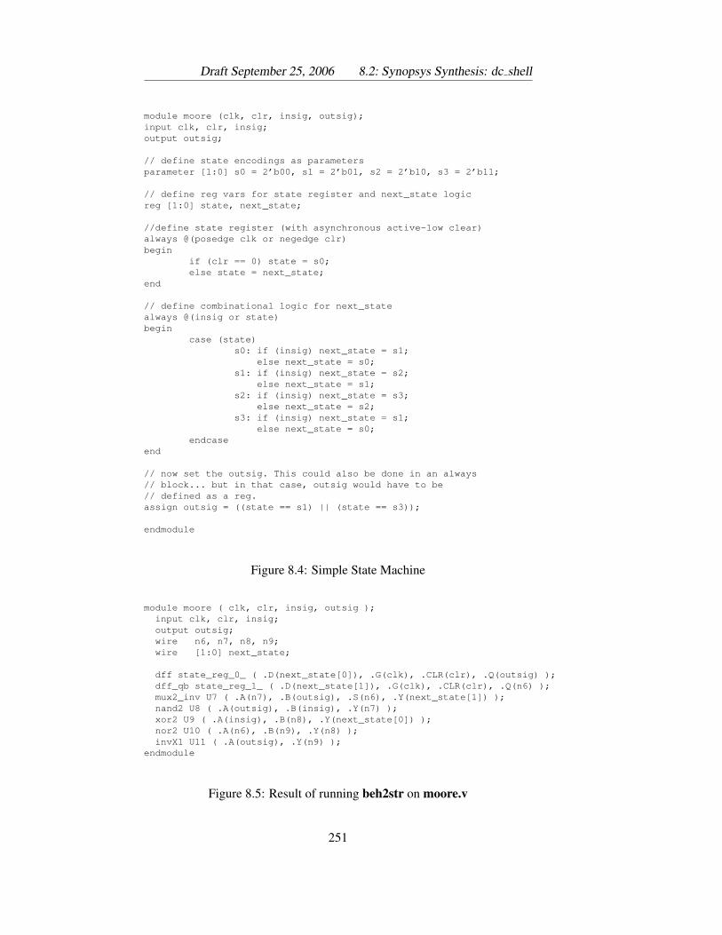
Draft September 25, 2006 8.2: Synopsys Synthesis: dc shell
module moore (clk, clr, insig, outsig);input clk, clr, insig;output outsig;
// define state encodings as parametersparameter [1:0] s0 = 2’b00, s1 = 2’b01, s2 = 2’b10, s3 = 2’b11;
// define reg vars for state register and next_state logicreg [1:0] state, next_state;
//define state register (with asynchronous active-low clear)always @(posedge clk or negedge clr)begin
if (clr == 0) state = s0;else state = next_state;
end
// define combinational logic for next_statealways @(insig or state)begin
case (state)s0: if (insig) next_state = s1;
else next_state = s0;s1: if (insig) next_state = s2;
else next_state = s1;s2: if (insig) next_state = s3;
else next_state = s2;s3: if (insig) next_state = s1;
else next_state = s0;endcase
end
// now set the outsig. This could also be done in an always// block... but in that case, outsig would have to be// defined as a reg.assign outsig = ((state == s1) || (state == s3));
endmodule
Figure 8.4: Simple State Machine
module moore ( clk, clr, insig, outsig );input clk, clr, insig;output outsig;wire n6, n7, n8, n9;wire [1:0] next_state;
dff state_reg_0_ ( .D(next_state[0]), .G(clk), .CLR(clr), .Q(outsig) );dff_qb state_reg_1_ ( .D(next_state[1]), .G(clk), .CLR(clr), .Q(n6) );mux2_inv U7 ( .A(n7), .B(outsig), .S(n6), .Y(next_state[1]) );nand2 U8 ( .A(outsig), .B(insig), .Y(n7) );xor2 U9 ( .A(insig), .B(n8), .Y(next_state[0]) );nor2 U10 ( .A(n6), .B(n9), .Y(n8) );invX1 U11 ( .A(outsig), .Y(n9) );
endmodule
Figure 8.5: Result of running beh2str on moore.v
251
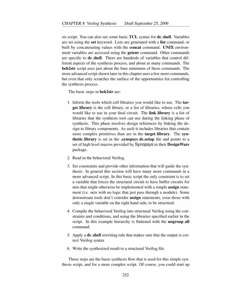
CHAPTER 8: Verilog Synthesis Draft September 25, 2006
sis script. You can also see some basic TCL syntax for dc shell. Variablesare set using the set keyword. Lists are generated with a list command, orbuilt by concatenating values with the concat command. UNIX environ-ment variables are accessed using the getenv command. Other commandsare specific to dc shell. There are hundreds of variables that control dif-ferent aspects of the synthesis process, and about as many commands. Thebeh2str script uses just about the bare minimum of these commands. Themore advanced script shown later in this chapter uses a few more commands,but even that only scratches the surface of the opportunities for controllingthe synthesis process.
The basic steps in beh2str are:
1. Inform the tools which cell libraries you would like to use. The tar-get library is the cell library, or a list of libraries, whose cells youwould like to use in your final circuit. The link library is a list oflibraries that the synthesis tool can use during the linking phase ofsynthesis. This phase resolves design references by linking the de-sign to library components. As such it includes libraries that containmore complex primitives than are in the target library. The syn-thetic library is set in the .synopsys dc.setup file and points to aset of high level macros provided by Synopsys in their DesignWarepackage.
2. Read in the behavioral Verilog.
3. Set constraints and provide other information that will guide the syn-thesis. In general this section will have many more commands in amore advanced script. In this basic script the only constraint is to seta variable that forces the structural circuit to have buffer circuits fornets that might otherwise be implemented with a simple assign state-ment (i.e. nets with no logic that just pass through a module). Somedownstream tools don’t consider assign statements, even those withonly a single variable on the right hand side, to be structural.
4. Compile the behavioral Verilog into structural Verilog using the con-straints and conditions, and using the libraries specified earlier in thescript. In this example hierarchy is flattened with the ungroup allcommand.
5. Apply a dc shell rewriting rule that makes sure that the output is cor-rect Verilog syntax
6. Write the synthesized result to a structural Verilog file.
These steps are the basic synthesis flow that is used for this simple syn-thesis script, and for a more complex script. Of course, you could start up
252
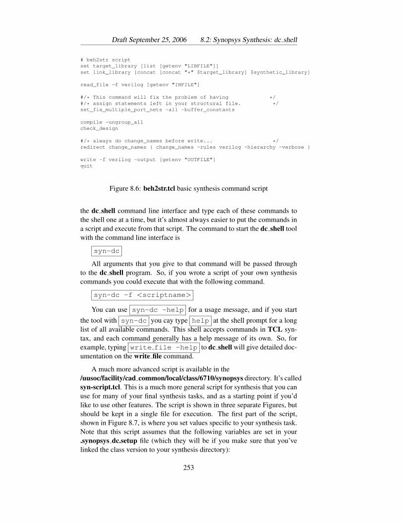
Draft September 25, 2006 8.2: Synopsys Synthesis: dc shell
# beh2str scriptset target_library [list [getenv "LIBFILE"]]set link_library [concat [concat "*" $target_library] $synthetic_library]
read_file -f verilog [getenv "INFILE"]
#/* This command will fix the problem of having */#/* assign statements left in your structural file. */set_fix_multiple_port_nets -all -buffer_constants
compile -ungroup_allcheck_design
#/* always do change_names before write... */redirect change_names { change_names -rules verilog -hierarchy -verbose }
write -f verilog -output [getenv "OUTFILE"]quit
Figure 8.6: beh2str.tcl basic synthesis command script
the dc shell command line interface and type each of these commands tothe shell one at a time, but it’s almost always easier to put the commands ina script and execute from that script. The command to start the dc shell toolwith the command line interface is
syn-dc
All arguments that you give to that command will be passed throughto the dc shell program. So, if you wrote a script of your own synthesiscommands you could execute that with the following command.
syn-dc -f <scriptname>
You can use syn-dc -help for a usage message, and if you startthe tool with syn-dc you cay type help at the shell prompt for a longlist of all available commands. This shell accepts commands in TCL syn-tax, and each command generally has a help message of its own. So, forexample, typing write file -help to dc shell will give detailed doc-umentation on the write file command.
A much more advanced script is available in the/uusoc/facility/cad common/local/class/6710/synopsys directory. It’s calledsyn-script.tcl. This is a much more general script for synthesis that you canuse for many of your final synthesis tasks, and as a starting point if you’dlike to use other features. The script is shown in three separate Figures, butshould be kept in a single file for execution. The first part of the script,shown in Figure 8.7, is where you set values specific to your synthesis task.Note that this script assumes that the following variables are set in your.synopsys dc.setup file (which they will be if you make sure that you’velinked the class version to your synthesis directory):
253
CHAPTER 8: Verilog Synthesis Draft September 25, 2006
SynopsysInstall: The path to the main synopsys installation directory
synthetic library: The path to the DesignWare files
symbol library: The path to a library of generic logic symbols for makingschematics
In this first part of the syn-script.tcl file you need to modify things foryour specific synthesis task. You should look at each line carefully, and inparticular you should change everything that has “!!” in front and back tothe correct values for your synthesis task. Some comments about the thingsto set follow:
• You need to set the name of your .db file as the target library, ormake this a list if you have multiple libraries with cell descriptions.
• You also need to list all of your Verilog behavioral files. The exampleshave all been with a single Verilog file, but in general a larger designwill most likely use multiple files.
• The basename is the basename that will be used for the output files.An extra descriptor will be appended to each output file to identifythem.
• myclk is the name of your clock signal. If your design has no clock(i.e. it’s combinational not sequential) you can use a virtual clock forpurposes of defining a speed target. Synopsys uses the timing of theclock signal to define a speed goal for the synthesis. A virtual clockis a name not attached to any wire in your circuit that can be used forthis speed goal if you don’t actually have a clock.
• The useUltra switch defines whether to use “ultra mode” for compil-ing or not. Unless you have very specific reasons to drive the synthesisdirectly, “ultra mode” will probably give you the best results.
• The timing section is where you set speed goals for the synthesis. Thenumbers are in ns. A period of 10 would set a speed goal of 100MHz,for example.
• The other delays define how inputs from other circuits and outputs toother circuits will behave. That is, how will this synthesized circuitconnect to other circuits.
• The myinputbuf variable should be set to the name of the cell inyour library that is an example of what would be driving the externalinputs to your circuit, and the myloadcell variable should be the nameof the pin on a cell in your library that represents the output load of
254
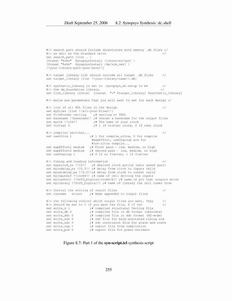
Draft September 25, 2006 8.2: Synopsys Synthesis: dc shell
#/* search path should include directories with memory .db files */#/* as well as the standard cells */set search_path [list . \[format "%s%s" SynopsysInstall /libraries/syn] \[format "%s%s" SynopsysInstall /dw/sim_ver] \!!your-library-path-goes-here!!]
#/* target library list should include all target .db files */set target_library [list !!your-library-name!!.db]
#/* synthetic_library is set in .synopsys_dc.setup to be */#/* the dw_foundation library. */set link_library [concat [concat "*" $target_library] $synthetic_library]
#/* below are parameters that you will want to set for each design */
#/* list of all HDL files in the design */set myfiles [list !!all-your-files!!]set fileFormat verilog ;# verilog or VHDLset basename !!basename!! ;# choose a basename for the output filesset myclk !!clk!! ;# The name of your clockset virtual 0 ;# 1 if virtual clock, 0 if real clock
#/* compiler switches... */set useUltra 1 ;# 1 for compile_ultra, 0 for compile
#mapEffort, useUngroup are for#non-ultra compile...
set mapEffort1 medium ;# First pass - low, medium, or highset mapEffort2 medium ;# second pass - low, medium, or highset useUngroup 1 ;# 0 if no flatten, 1 if flatten
#/* Timing and loading information */set myperiod_ns !!10!! ;# desired clock period (sets speed goal)set myindelay_ns !!0.5!! ;# delay from clock to inputs validset myoutdelay_ns !!0.5!!;# delay from clock to output validset myinputbuf !!invX4!! ;# name of cell driving the inputsset myloadcell !!UofU_Digital/invX4/A!! ;# name of pin that outputs driveset mylibrary !!UofU_Digital!! ;# name of library the cell comes from
#/* Control the writing of result files */set runname struct ;# Name appended to output files
#/* the following control which output files you want. They */#/* should be set to 1 if you want the file, 0 if not */set write_v 1 ;# compiled structural Verilog fileset write_db 0 ;# compiled file in db format (obsolete)set write_ddc 0 ;# compiled file in ddc format (XG-mode)set write_sdf 0 ;# sdf file for back-annotated timing simset write_sdc 0 ;# sdc constraint file for place and routeset write_rep 1 ;# report file from compilationset write_pow 0 ;# report file for power estimate
Figure 8.7: Part 1 of the syn-script.tcl synthesis script
255
CHAPTER 8: Verilog Synthesis Draft September 25, 2006
an external output. The example in Figure 8.7 references the A inputof the invX4 inverter in the UofU Digital library (also defined as thetarget library. These must be names of cells and cell inputs in oneof your target libraries.
• The write flags define which outputs should be generated by the syn-thesis process. You almost certainly want to generate a structural Ver-ilog file. You will usually also want at least a report file for timingand area reports. The other output files are used for other phases ofthe total flow. The ddc file is the Synopsys binary database format.You can save the synthesized circuit in .ddc format for ease of read-ing it back in to Synopsys for further processing. The .sdf and .sdcfiles are timing and constraint files that are used later in the flow. Thepower report uses power information in the .db file to generate a veryrough estimate of power usage by your design.
.
The second part of the syn-script.tcl is seen in Figure 8.8. It containsthe synthesis commands that use the variables you set in the first part of thefile. You shouldn’t have to modify anything in this part of the file unlessyou’d like to change how the synthesis proceeds. Note that the read com-mand from beh2str has been replaced with a two-step process of analyzeand elaborate. This is because if you have multiple Verilog files to syn-thesize, you need to analyze them all first before combining them togetherand synthesizing them. The other commands are documented in the script.You can see that constraints are set according to your information in part1.Finally the design is compiled, checked, and violations are checked.
The third part of the syn-script.tcl file is where the outputs are writtenout. It’s pretty straightforward. Note that when you write the structural Ver-ilog output you also change names to make sure that the output is in correctVerilog syntax. You’d think that this would be part of the write command,but it’s not. The output file names are constructed from basename and run-name which are set in the first part of the file.
8.2.1 Small Example: A Finite State Machine
As an example, if the moore.v Verilog file in Figure 8.4 was compiledwith this script, I would set the target library to UofU Digital.db, includemoore.v in the myfiles list, use a basename of moore, a myclk of clk, anduse the ultra mode with useUltra. With a speed goal of 10ns period andthe input buffer and output load set as in the example, the result is seen inFigure 8.10. Note that it’s almost the same as the simple result in Figure 8.5(which would expect for such a simple Verilog behavioral description), but
256
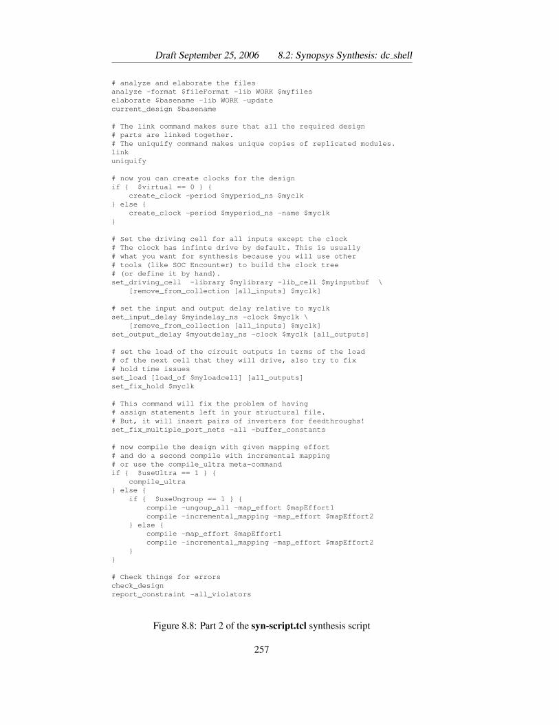
Draft September 25, 2006 8.2: Synopsys Synthesis: dc shell
# analyze and elaborate the filesanalyze -format $fileFormat -lib WORK $myfileselaborate $basename -lib WORK -updatecurrent_design $basename
# The link command makes sure that all the required design# parts are linked together.# The uniquify command makes unique copies of replicated modules.linkuniquify
# now you can create clocks for the designif { $virtual == 0 } {
create_clock -period $myperiod_ns $myclk} else {
create_clock -period $myperiod_ns -name $myclk}
# Set the driving cell for all inputs except the clock# The clock has infinte drive by default. This is usually# what you want for synthesis because you will use other# tools (like SOC Encounter) to build the clock tree# (or define it by hand).set_driving_cell -library $mylibrary -lib_cell $myinputbuf \
[remove_from_collection [all_inputs] $myclk]
# set the input and output delay relative to myclkset_input_delay $myindelay_ns -clock $myclk \
[remove_from_collection [all_inputs] $myclk]set_output_delay $myoutdelay_ns -clock $myclk [all_outputs]
# set the load of the circuit outputs in terms of the load# of the next cell that they will drive, also try to fix# hold time issuesset_load [load_of $myloadcell] [all_outputs]set_fix_hold $myclk
# This command will fix the problem of having# assign statements left in your structural file.# But, it will insert pairs of inverters for feedthroughs!set_fix_multiple_port_nets -all -buffer_constants
# now compile the design with given mapping effort# and do a second compile with incremental mapping# or use the compile_ultra meta-commandif { $useUltra == 1 } {
compile_ultra} else {
if { $useUngroup == 1 } {compile -ungoup_all -map_effort $mapEffort1compile -incremental_mapping -map_effort $mapEffort2
} else {compile -map_effort $mapEffort1compile -incremental_mapping -map_effort $mapEffort2
}}
# Check things for errorscheck_designreport_constraint -all_violators
Figure 8.8: Part 2 of the syn-script.tcl synthesis script
257
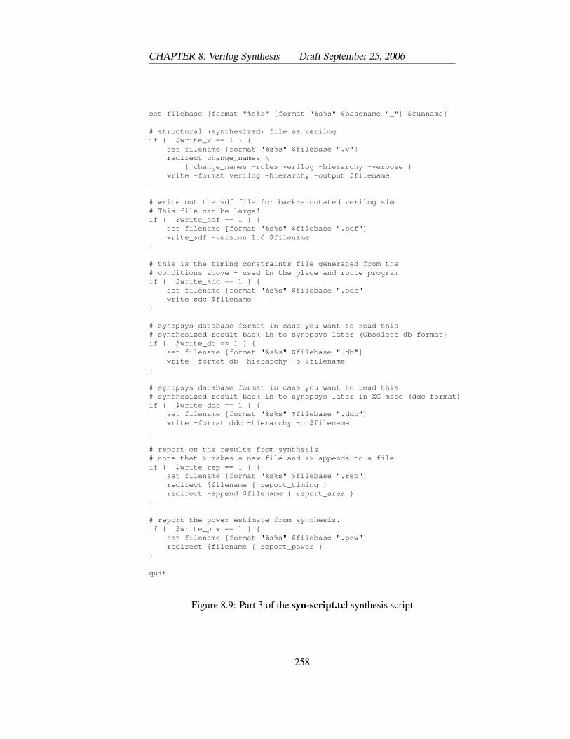
CHAPTER 8: Verilog Synthesis Draft September 25, 2006
set filebase [format "%s%s" [format "%s%s" $basename "_"] $runname]
# structural (synthesized) file as verilogif { $write_v == 1 } {
set filename [format "%s%s" $filebase ".v"]redirect change_names \
{ change_names -rules verilog -hierarchy -verbose }write -format verilog -hierarchy -output $filename
}
# write out the sdf file for back-annotated verilog sim# This file can be large!if { $write_sdf == 1 } {
set filename [format "%s%s" $filebase ".sdf"]write_sdf -version 1.0 $filename
}
# this is the timing constraints file generated from the# conditions above - used in the place and route programif { $write_sdc == 1 } {
set filename [format "%s%s" $filebase ".sdc"]write_sdc $filename
}
# synopsys database format in case you want to read this# synthesized result back in to synopsys later (Obsolete db format)if { $write_db == 1 } {
set filename [format "%s%s" $filebase ".db"]write -format db -hierarchy -o $filename
}
# synopsys database format in case you want to read this# synthesized result back in to synopsys later in XG mode (ddc format)if { $write_ddc == 1 } {
set filename [format "%s%s" $filebase ".ddc"]write -format ddc -hierarchy -o $filename
}
# report on the results from synthesis# note that > makes a new file and >> appends to a fileif { $write_rep == 1 } {
set filename [format "%s%s" $filebase ".rep"]redirect $filename { report_timing }redirect -append $filename { report_area }
}
# report the power estimate from synthesis.if { $write_pow == 1 } {
set filename [format "%s%s" $filebase ".pow"]redirect $filename { report_power }
}
quit
Figure 8.9: Part 3 of the syn-script.tcl synthesis script
258
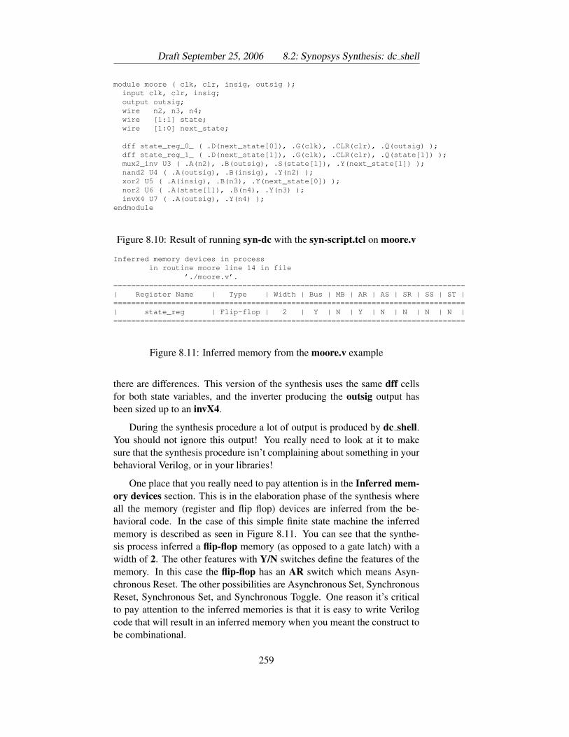
Draft September 25, 2006 8.2: Synopsys Synthesis: dc shell
module moore ( clk, clr, insig, outsig );input clk, clr, insig;output outsig;wire n2, n3, n4;wire [1:1] state;wire [1:0] next_state;
dff state_reg_0_ ( .D(next_state[0]), .G(clk), .CLR(clr), .Q(outsig) );dff state_reg_1_ ( .D(next_state[1]), .G(clk), .CLR(clr), .Q(state[1]) );mux2_inv U3 ( .A(n2), .B(outsig), .S(state[1]), .Y(next_state[1]) );nand2 U4 ( .A(outsig), .B(insig), .Y(n2) );xor2 U5 ( .A(insig), .B(n3), .Y(next_state[0]) );nor2 U6 ( .A(state[1]), .B(n4), .Y(n3) );invX4 U7 ( .A(outsig), .Y(n4) );
endmodule
Figure 8.10: Result of running syn-dc with the syn-script.tcl on moore.v
Inferred memory devices in processin routine moore line 14 in file
’./moore.v’.===============================================================================| Register Name | Type | Width | Bus | MB | AR | AS | SR | SS | ST |===============================================================================| state_reg | Flip-flop | 2 | Y | N | Y | N | N | N | N |===============================================================================
Figure 8.11: Inferred memory from the moore.v example
there are differences. This version of the synthesis uses the same dff cellsfor both state variables, and the inverter producing the outsig output hasbeen sized up to an invX4.
During the synthesis procedure a lot of output is produced by dc shell.You should not ignore this output! You really need to look at it to makesure that the synthesis procedure isn’t complaining about something in yourbehavioral Verilog, or in your libraries!
One place that you really need to pay attention is in the Inferred mem-ory devices section. This is in the elaboration phase of the synthesis whereall the memory (register and flip flop) devices are inferred from the be-havioral code. In the case of this simple finite state machine the inferredmemory is described as seen in Figure 8.11. You can see that the synthe-sis process inferred a flip-flop memory (as opposed to a gate latch) with awidth of 2. The other features with Y/N switches define the features of thememory. In this case the flip-flop has an AR switch which means Asyn-chronous Reset. The other possibilities are Asynchronous Set, SynchronousReset, Synchronous Set, and Synchronous Toggle. One reason it’s criticalto pay attention to the inferred memories is that it is easy to write Verilogcode that will result in an inferred memory when you meant the construct tobe combinational.
259
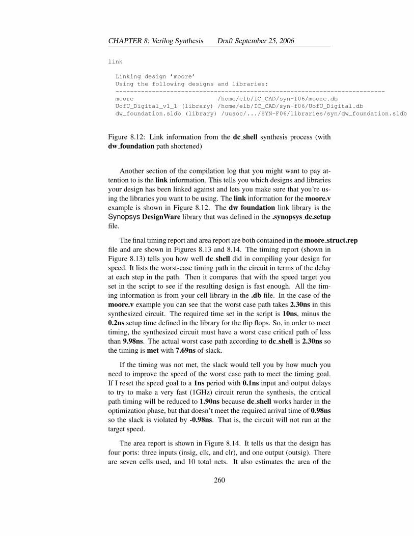
CHAPTER 8: Verilog Synthesis Draft September 25, 2006
link
Linking design ’moore’Using the following designs and libraries:--------------------------------------------------------------------------moore /home/elb/IC_CAD/syn-f06/moore.dbUofU_Digital_v1_1 (library) /home/elb/IC_CAD/syn-f06/UofU_Digital.dbdw_foundation.sldb (library) /uusoc/.../SYN-F06/libraries/syn/dw_foundation.sldb
Figure 8.12: Link information from the dc shell synthesis process (withdw foundation path shortened)
Another section of the compilation log that you might want to pay at-tention to is the link information. This tells you which designs and librariesyour design has been linked against and lets you make sure that you’re us-ing the libraries you want to be using. The link information for the moore.vexample is shown in Figure 8.12. The dw foundation link library is theSynopsys DesignWare library that was defined in the .synopsys dc.setupfile.
The final timing report and area report are both contained in the moore struct.repfile and are shown in Figures 8.13 and 8.14. The timing report (shown inFigure 8.13) tells you how well dc shell did in compiling your design forspeed. It lists the worst-case timing path in the circuit in terms of the delayat each step in the path. Then it compares that with the speed target youset in the script to see if the resulting design is fast enough. All the tim-ing information is from your cell library in the .db file. In the case of themoore.v example you can see that the worst case path takes 2.30ns in thissynthesized circuit. The required time set in the script is 10ns, minus the0.2ns setup time defined in the library for the flip flops. So, in order to meettiming, the synthesized circuit must have a worst case critical path of lessthan 9.98ns. The actual worst case path according to dc shell is 2.30ns sothe timing is met with 7.69ns of slack.
If the timing was not met, the slack would tell you by how much youneed to improve the speed of the worst case path to meet the timing goal.If I reset the speed goal to a 1ns period with 0.1ns input and output delaysto try to make a very fast (1GHz) circuit rerun the synthesis, the criticalpath timing will be reduced to 1.90ns because dc shell works harder in theoptimization phase, but that doesn’t meet the required arrival time of 0.98nsso the slack is violated by -0.98ns. That is, the circuit will not run at thetarget speed.
The area report is shown in Figure 8.14. It tells us that the design hasfour ports: three inputs (insig, clk, and clr), and one output (outsig). Thereare seven cells used, and 10 total nets. It also estimates the area of the
260
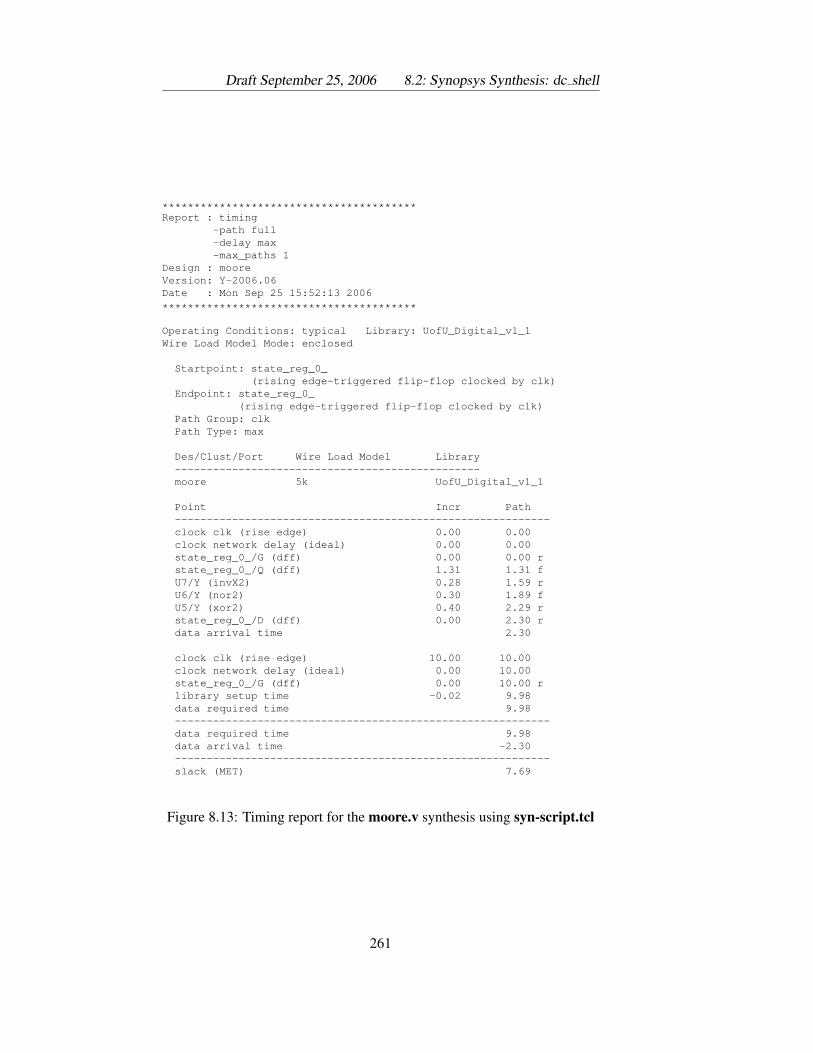
Draft September 25, 2006 8.2: Synopsys Synthesis: dc shell
****************************************Report : timing
-path full-delay max-max_paths 1
Design : mooreVersion: Y-2006.06Date : Mon Sep 25 15:52:13 2006
****************************************
Operating Conditions: typical Library: UofU_Digital_v1_1Wire Load Model Mode: enclosed
Startpoint: state_reg_0_(rising edge-triggered flip-flop clocked by clk)
Endpoint: state_reg_0_(rising edge-triggered flip-flop clocked by clk)
Path Group: clkPath Type: max
Des/Clust/Port Wire Load Model Library------------------------------------------------moore 5k UofU_Digital_v1_1
Point Incr Path-----------------------------------------------------------clock clk (rise edge) 0.00 0.00clock network delay (ideal) 0.00 0.00state_reg_0_/G (dff) 0.00 0.00 rstate_reg_0_/Q (dff) 1.31 1.31 fU7/Y (invX2) 0.28 1.59 rU6/Y (nor2) 0.30 1.89 fU5/Y (xor2) 0.40 2.29 rstate_reg_0_/D (dff) 0.00 2.30 rdata arrival time 2.30
clock clk (rise edge) 10.00 10.00clock network delay (ideal) 0.00 10.00state_reg_0_/G (dff) 0.00 10.00 rlibrary setup time -0.02 9.98data required time 9.98-----------------------------------------------------------data required time 9.98data arrival time -2.30-----------------------------------------------------------slack (MET) 7.69
Figure 8.13: Timing report for the moore.v synthesis using syn-script.tcl
261
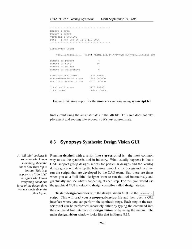
CHAPTER 8: Verilog Synthesis Draft September 25, 2006
****************************************Report : areaDesign : mooreVersion: Y-2006.06Date : Mon Sep 25 15:24:12 2006
****************************************
Library(s) Used:
UofU_Digital_v1_1 (File: /home/elb/IC_CAD/syn-f06/UofU_Digital.db)
Number of ports: 4Number of nets: 10Number of cells: 7Number of references: 6
Combinational area: 1231.199951Noncombinational area: 1944.000000Net Interconnect area: 8470.000000
Total cell area: 3175.199951Total area: 11645.200195
Figure 8.14: Area report for the moore.v synthesis using syn-script.tcl
final circuit using the area estimates in the .db file. This area does not takeplacement and routing into account so it’s just approximate.
8.3 Synopsys Synthesis: Design Vision GUI
Running dc shell with a script (like syn-script.tcl is the most commonA “tall thin” designer issomeone who knowssomething about the
entire flow from top tobottom. This is as
oppose to a “short fat”designer who knowseverything about one
layer of the design flow,but not much about the
other layers.
way to use the synthesis tool in industry. What usually happens is that aCAD support group designs scripts for particular designs and the Verilogdesign group will develop the behavioral model of the design and then justrun the scripts that are developed by the CAD team. But, there are timeswhen you as a “tall thin” designer want to run the tool interactively andgraphically and see what’s happening at each step. For this, you would usethe graphical GUI interface to design compiler called design vision.
To start design compiler with the design vision GUI use the syn-dvscript. This will read your .synopsys dc.setup file and then open a GUIinterface where you can perform the synthesis steps. Each step in the syn-script.tcl can be performed separately either by typing the command intothe command line interface of design vision or by using the menus. Themain design vision window looks like that in Figure 8.15.
262
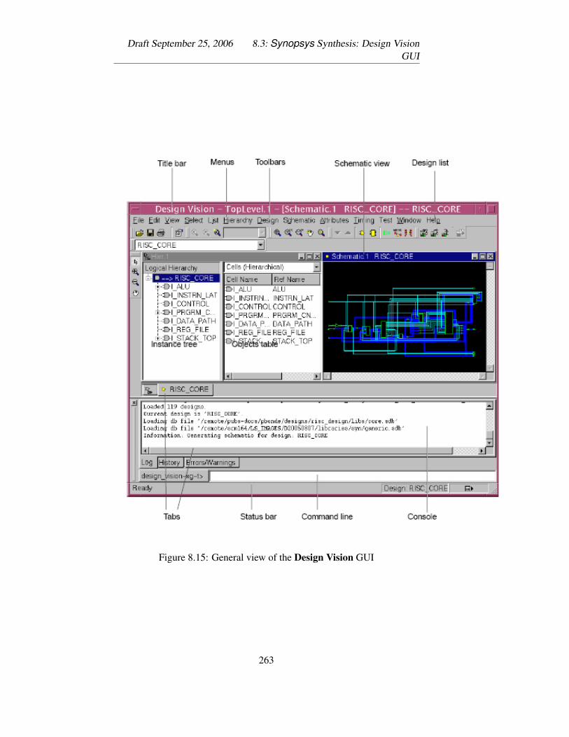
Draft September 25, 2006 8.3: Synopsys Synthesis: Design VisionGUI
Figure 8.15: General view of the Design Vision GUI
263
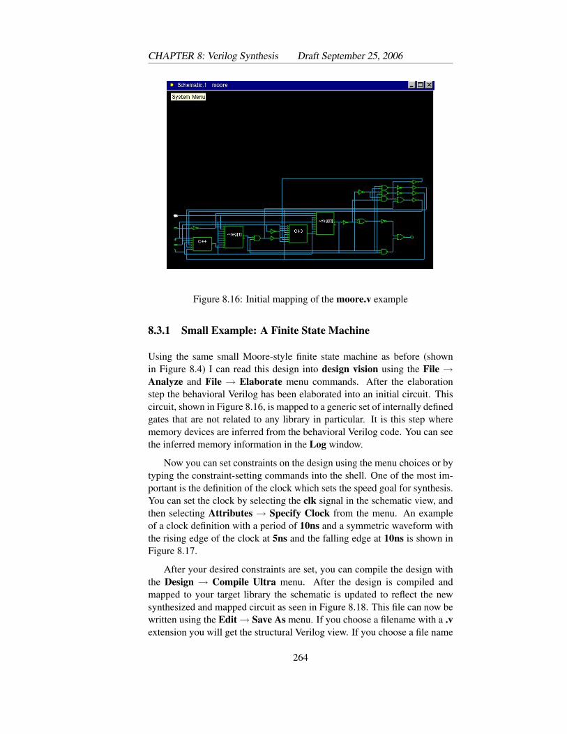
CHAPTER 8: Verilog Synthesis Draft September 25, 2006
Figure 8.16: Initial mapping of the moore.v example
8.3.1 Small Example: A Finite State Machine
Using the same small Moore-style finite state machine as before (shownin Figure 8.4) I can read this design into design vision using the File →Analyze and File → Elaborate menu commands. After the elaborationstep the behavioral Verilog has been elaborated into an initial circuit. Thiscircuit, shown in Figure 8.16, is mapped to a generic set of internally definedgates that are not related to any library in particular. It is this step wherememory devices are inferred from the behavioral Verilog code. You can seethe inferred memory information in the Log window.
Now you can set constraints on the design using the menu choices or bytyping the constraint-setting commands into the shell. One of the most im-portant is the definition of the clock which sets the speed goal for synthesis.You can set the clock by selecting the clk signal in the schematic view, andthen selecting Attributes → Specify Clock from the menu. An exampleof a clock definition with a period of 10ns and a symmetric waveform withthe rising edge of the clock at 5ns and the falling edge at 10ns is shown inFigure 8.17.
After your desired constraints are set, you can compile the design withthe Design → Compile Ultra menu. After the design is compiled andmapped to your target library the schematic is updated to reflect the newsynthesized and mapped circuit as seen in Figure 8.18. This file can now bewritten using the Edit → Save As menu. If you choose a filename with a .vextension you will get the structural Verilog view. If you choose a file name
264
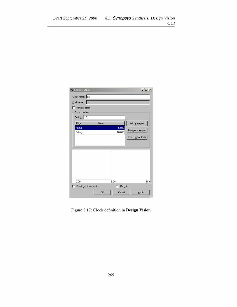
Draft September 25, 2006 8.3: Synopsys Synthesis: Design VisionGUI
Figure 8.17: Clock definition in Design Vision
265
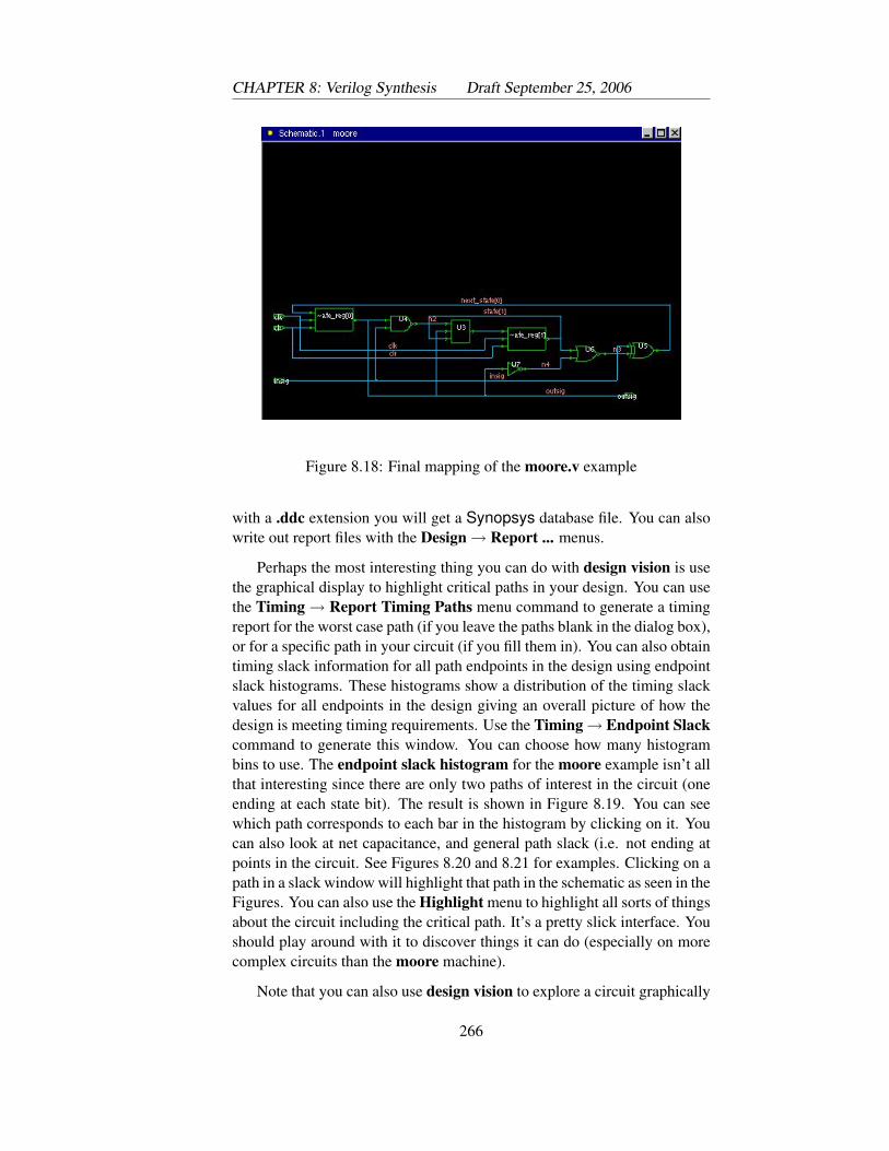
CHAPTER 8: Verilog Synthesis Draft September 25, 2006
Figure 8.18: Final mapping of the moore.v example
with a .ddc extension you will get a Synopsys database file. You can alsowrite out report files with the Design → Report ... menus.
Perhaps the most interesting thing you can do with design vision is usethe graphical display to highlight critical paths in your design. You can usethe Timing → Report Timing Paths menu command to generate a timingreport for the worst case path (if you leave the paths blank in the dialog box),or for a specific path in your circuit (if you fill them in). You can also obtaintiming slack information for all path endpoints in the design using endpointslack histograms. These histograms show a distribution of the timing slackvalues for all endpoints in the design giving an overall picture of how thedesign is meeting timing requirements. Use the Timing→ Endpoint Slackcommand to generate this window. You can choose how many histogrambins to use. The endpoint slack histogram for the moore example isn’t allthat interesting since there are only two paths of interest in the circuit (oneending at each state bit). The result is shown in Figure 8.19. You can seewhich path corresponds to each bar in the histogram by clicking on it. Youcan also look at net capacitance, and general path slack (i.e. not ending atpoints in the circuit. See Figures 8.20 and 8.21 for examples. Clicking on apath in a slack window will highlight that path in the schematic as seen in theFigures. You can also use the Highlight menu to highlight all sorts of thingsabout the circuit including the critical path. It’s a pretty slick interface. Youshould play around with it to discover things it can do (especially on morecomplex circuits than the moore machine).
Note that you can also use design vision to explore a circuit graphically
266
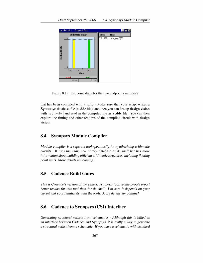
Draft September 25, 2006 8.4: Synopsys Module Compiler
Figure 8.19: Endpoint slack for the two endpoints in moore
that has been compiled with a script. Make sure that your script writes aSynopsys database file (a .ddc file), and then you can fire up design visionwith syn-dv and read in the compiled file as a .ddc file. You can thenexplore the timing and other features of the compiled circuit with designvision.
8.4 Synopsys Module Compiler
Module compiler is a separate tool specifically for synthesizing arithmeticcircuits. It uses the same cell library database as dc shell but has moreinformation about building efficient arithmetic structures, including floatingpoint units. More details are coming!
8.5 Cadence Build Gates
This is Cadence’s version of the generic synthesis tool. Some people reportbetter results for this tool than for dc shell. I’m sure it depends on yourcircuit and your familiarity with the tools. More details are coming!
8.6 Cadence to Synopsys (CSI) Interface
Generating structural netlists from schematics - Although this is billed asan interface between Cadence and Synopsys, it is really a way to generatea structural netlist from a schematic. If you have a schematic with standard
267
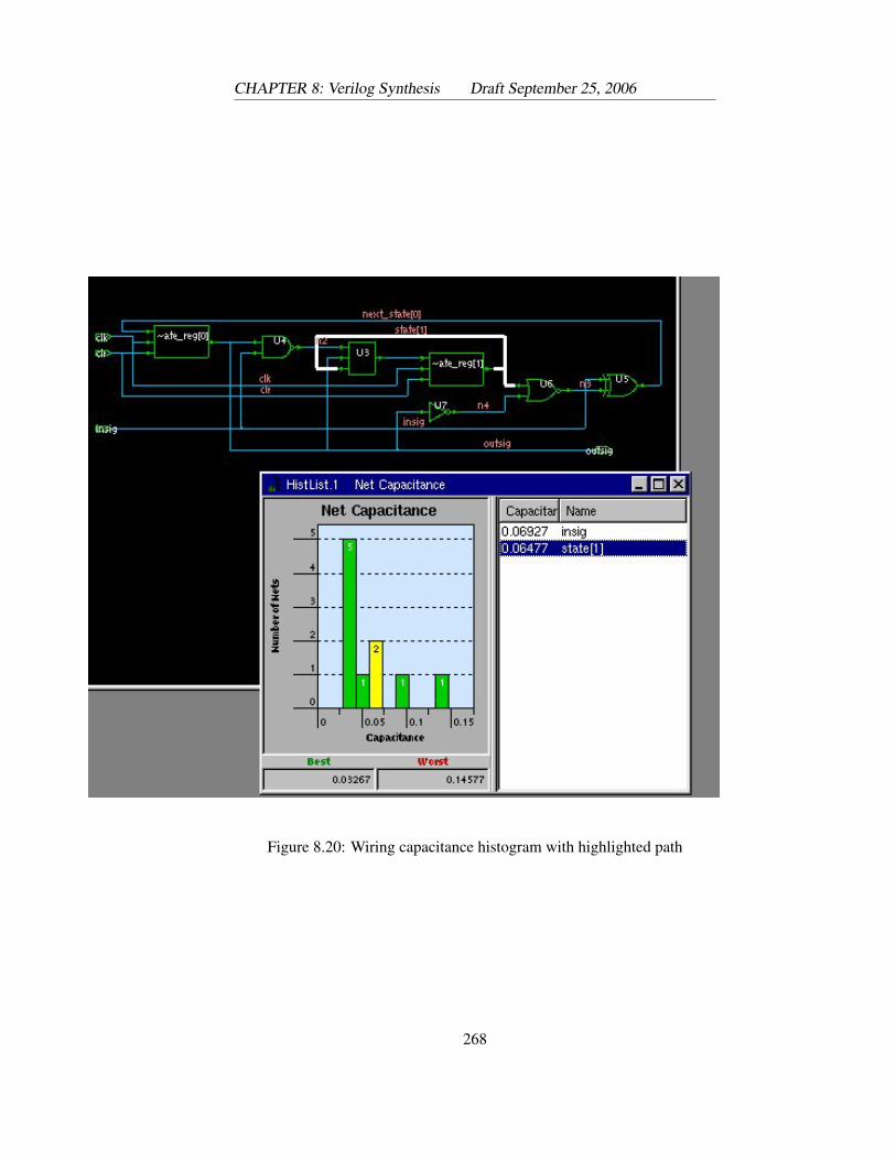
CHAPTER 8: Verilog Synthesis Draft September 25, 2006
Figure 8.20: Wiring capacitance histogram with highlighted path
268
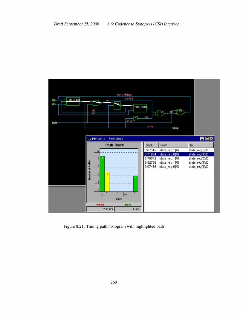
Draft September 25, 2006 8.6: Cadence to Synopsys (CSI) Interface
Figure 8.21: Timing path histogram with highlighted path
269

CHAPTER 8: Verilog Synthesis Draft September 25, 2006
cells gates, this will generate a netlist that only goes down to those gates, andnot descend all the way to the transistors as would happen for simulation.More details are coming!
270
Chapter 9
Abstract Generation
IN ORDER for the place and route tool to do its job, it needs to knowcertain physical information about the cells in the library it is using.For example, it needs to know the bounding box of each cell so it can
use that bounding box when it places cells next to each other. Note that thisbounding box may be described by the furthest pieces of geometry in thelayout view of the cell, or it may be offset from the layout so that the cellgeometry overlaps or has a gap when it is placed next to another cell. Theplace and route tool doesn’t need to know anything about the layout. It justplaces the cells according to their bounding box.
The other critical information for the place and route tool is the signalconnection points on the cells. It needs to know where the power and groundconnections are, and the signal connections so that it can wire the cells to-gether. It also needs to know just enough about the layout geometry of thecells so that it know where it can and can’t place wires over the top of thecell.
A view of the cell that has only this information about the cell (boundingbox, signal connections, and wiring blockages) is called an abstract view.An abstract view has much less information than the full layout view whichis useful for two reasons: it’s smaller and therefore less trouble to read, andit doesn’t have full layout information so cell library vendors can easilyrelease their abstract views while keeping the customers from seeing thefull layout views and thus retain their proprietary layout.
As an example, consider a simple inverter. Figure 9.1 shows the layoutview side by side with the abstract view. You can see that the abstract isvery simple compared to the layout. The abstract view doesn’t need anyinformation about any layers that aren’t directly used by the place and routeprogram. Because the place and route program uses only the metal layersfor routing, only the metal layers show up in the abstract. This example
CHAPTER 9: Abstract Generation Draft September 28, 2006
actually has four connection points: A (input), Y (output), and vdd (the topmetal piece) and gnd (the bottom metal piece). Note that the power andground connections are designed to abut (actually overlap) when the cellsare placed next to each other with their bounding boxes touching.
9.1 Abstract Tool
We, of course, have full layout views because that’s what we’ve been de-signing. The tool that extracts the abstract information from the full layoutview is called, appropriately enough, abstract and it can be run from yourcadence directory using the cad-abstract script.
Before you run abstract you need to have layout and extracted views(at least) of the cells that you wish to generate the abstracts of. Connectto the directory from which you run Cadence, and fire up the tool withcad-abstract . The abstract tool will now have access to your design
libraries that you’ve been using in Cadence.
9.1.1 Reading your Library into Abstract
When you start up abstract you’ll get a command window. All the majorYou can also get shorthelp on many things by
hovering your mouseover the object.
operations in generating abstracts can be initiated with the widgets near thetop of the window or by using the menus. The far-left widget that lookslike a book is used to load a Cadence library into abstract. The first stepin generating abstract views is to load a library that contains your cells.Figure 9.2 shows the Open Library box where I’m choosing my abs-testlibrary.
Once you’ve loaded your library you should see all the cell names inyour library sorted into bins. the Core bin will contain the cells that ab-stract thinks will be general core cells. The Ignore bin are the cells thatit will ignore. The other bins (IO, Corner, Block) are related to pad I/Oand pre-designed blocks. We won’t use them for our cell library. If you areonly interested in generating abstracts for some of your cells you can usethe Cells → Move... menu choice to move cells to different bins. By mov-ing cells to the Ignore bin, for example, you can exclude them from furtherprocessing. My example library has 11 cells that I would like to processinto abstract views, and 2 that I want to ignore. The window looks likethat in Figure 9.3. Note that you may have warnings that you don’t alreadyhave abstract views. You can ignore them. You should, however, see greencheck marks by each cell in the layout column to indicate that the layouthas been successfully read. If you see an orange exclamation point insteadthat means that there was some issue when the cell was read into abstract.
278
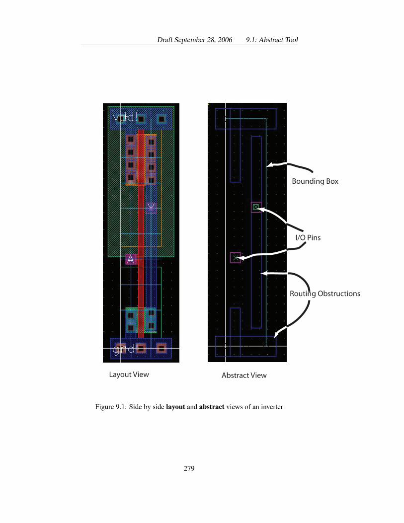
Draft September 28, 2006 9.1: Abstract Tool
Layout View Abstract View
Bounding Box
I/O Pins
Routing Obstructions
Figure 9.1: Side by side layout and abstract views of an inverter
279
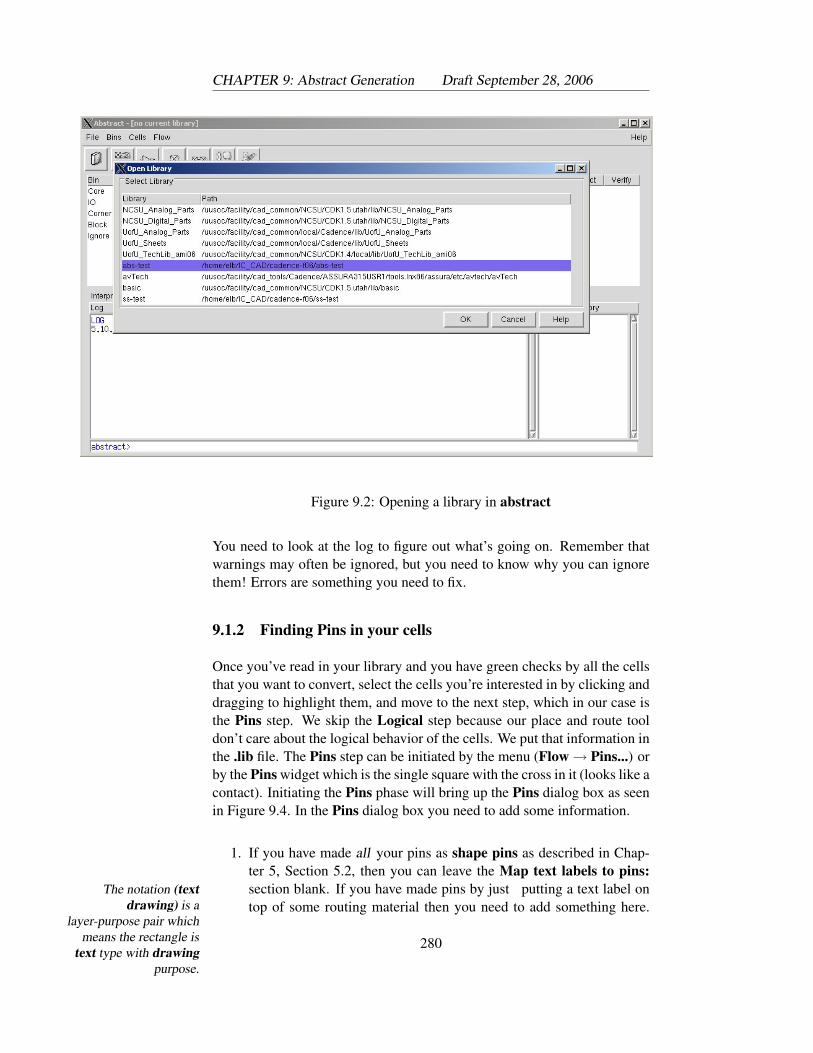
CHAPTER 9: Abstract Generation Draft September 28, 2006
Figure 9.2: Opening a library in abstract
You need to look at the log to figure out what’s going on. Remember thatwarnings may often be ignored, but you need to know why you can ignorethem! Errors are something you need to fix.
9.1.2 Finding Pins in your cells
Once you’ve read in your library and you have green checks by all the cellsthat you want to convert, select the cells you’re interested in by clicking anddragging to highlight them, and move to the next step, which in our case isthe Pins step. We skip the Logical step because our place and route tooldon’t care about the logical behavior of the cells. We put that information inthe .lib file. The Pins step can be initiated by the menu (Flow → Pins...) orby the Pins widget which is the single square with the cross in it (looks like acontact). Initiating the Pins phase will bring up the Pins dialog box as seenin Figure 9.4. In the Pins dialog box you need to add some information.
1. If you have made all your pins as shape pins as described in Chap-ter 5, Section 5.2, then you can leave the Map text labels to pins:section blank. If you have made pins by just putting a text label onThe notation (text
drawing) is alayer-purpose pair which
means the rectangle istext type with drawing
purpose.
top of some routing material then you need to add something here.
280
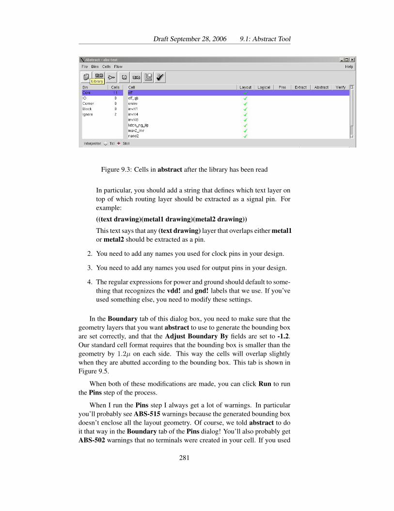
Draft September 28, 2006 9.1: Abstract Tool
Figure 9.3: Cells in abstract after the library has been read
In particular, you should add a string that defines which text layer ontop of which routing layer should be extracted as a signal pin. Forexample:
((text drawing)(metal1 drawing)(metal2 drawing))
This text says that any (text drawing) layer that overlaps either metal1or metal2 should be extracted as a pin.
2. You need to add any names you used for clock pins in your design.
3. You need to add any names you used for output pins in your design.
4. The regular expressions for power and ground should default to some-thing that recognizes the vdd! and gnd! labels that we use. If you’veused something else, you need to modify these settings.
In the Boundary tab of this dialog box, you need to make sure that thegeometry layers that you want abstract to use to generate the bounding boxare set correctly, and that the Adjust Boundary By fields are set to -1.2.Our standard cell format requires that the bounding box is smaller than thegeometry by 1.2µ on each side. This way the cells will overlap slightlywhen they are abutted according to the bounding box. This tab is shown inFigure 9.5.
When both of these modifications are made, you can click Run to runthe Pins step of the process.
When I run the Pins step I always get a lot of warnings. In particularyou’ll probably see ABS-515 warnings because the generated bounding boxdoesn’t enclose all the layout geometry. Of course, we told abstract to doit that way in the Boundary tab of the Pins dialog! You’ll also probably getABS-502 warnings that no terminals were created in your cell. If you used
281
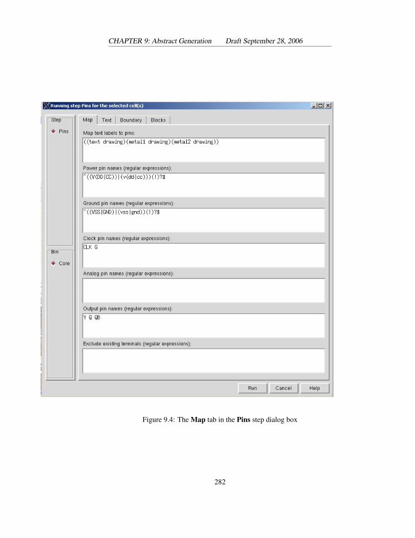
CHAPTER 9: Abstract Generation Draft September 28, 2006
Figure 9.4: The Map tab in the Pins step dialog box
282
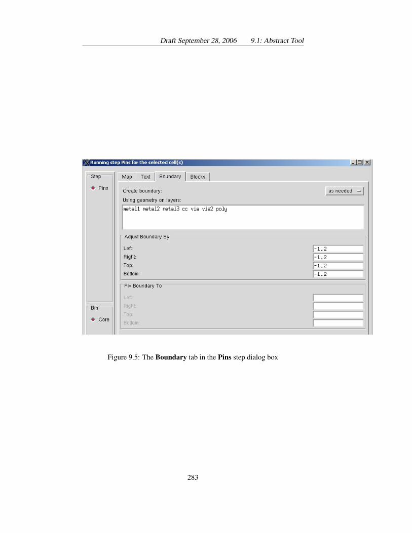
Draft September 28, 2006 9.1: Abstract Tool
Figure 9.5: The Boundary tab in the Pins step dialog box
283
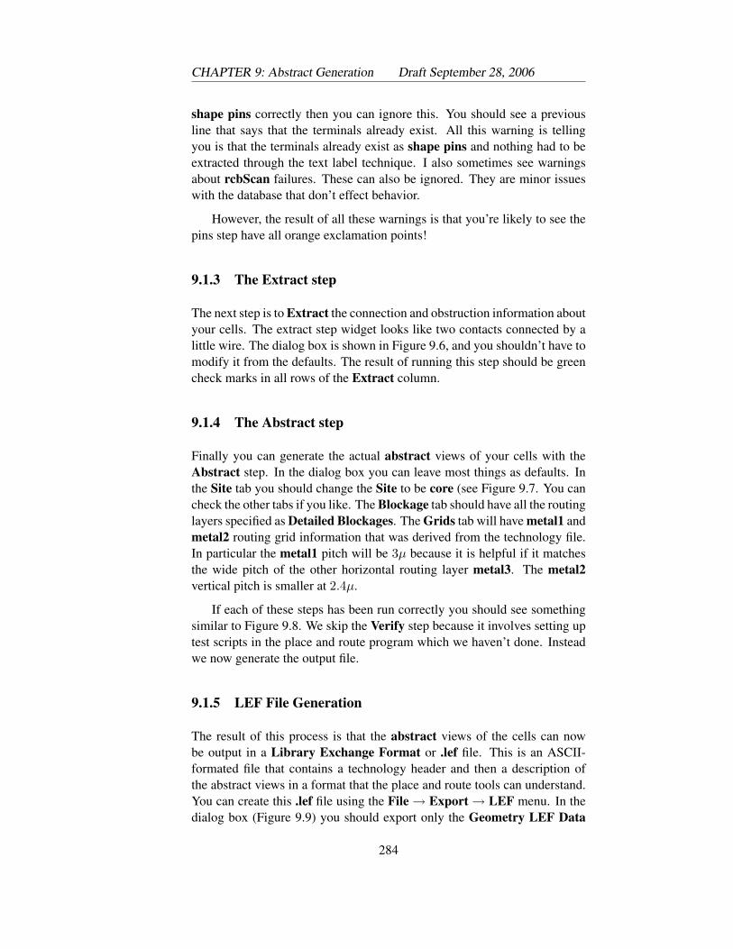
CHAPTER 9: Abstract Generation Draft September 28, 2006
shape pins correctly then you can ignore this. You should see a previousline that says that the terminals already exist. All this warning is tellingyou is that the terminals already exist as shape pins and nothing had to beextracted through the text label technique. I also sometimes see warningsabout rcbScan failures. These can also be ignored. They are minor issueswith the database that don’t effect behavior.
However, the result of all these warnings is that you’re likely to see thepins step have all orange exclamation points!
9.1.3 The Extract step
The next step is to Extract the connection and obstruction information aboutyour cells. The extract step widget looks like two contacts connected by alittle wire. The dialog box is shown in Figure 9.6, and you shouldn’t have tomodify it from the defaults. The result of running this step should be greencheck marks in all rows of the Extract column.
9.1.4 The Abstract step
Finally you can generate the actual abstract views of your cells with theAbstract step. In the dialog box you can leave most things as defaults. Inthe Site tab you should change the Site to be core (see Figure 9.7. You cancheck the other tabs if you like. The Blockage tab should have all the routinglayers specified as Detailed Blockages. The Grids tab will have metal1 andmetal2 routing grid information that was derived from the technology file.In particular the metal1 pitch will be 3µ because it is helpful if it matchesthe wide pitch of the other horizontal routing layer metal3. The metal2vertical pitch is smaller at 2.4µ.
If each of these steps has been run correctly you should see somethingsimilar to Figure 9.8. We skip the Verify step because it involves setting uptest scripts in the place and route program which we haven’t done. Insteadwe now generate the output file.
9.1.5 LEF File Generation
The result of this process is that the abstract views of the cells can nowbe output in a Library Exchange Format or .lef file. This is an ASCII-formated file that contains a technology header and then a description ofthe abstract views in a format that the place and route tools can understand.You can create this .lef file using the File → Export → LEF menu. In thedialog box (Figure 9.9) you should export only the Geometry LEF Data
284
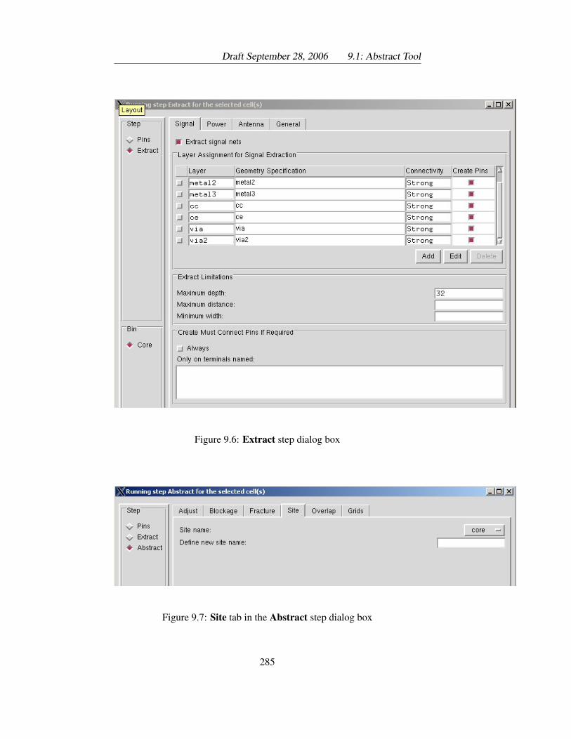
Draft September 28, 2006 9.1: Abstract Tool
Figure 9.6: Extract step dialog box
Figure 9.7: Site tab in the Abstract step dialog box
285
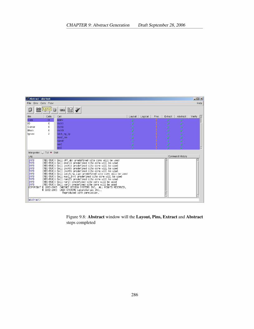
CHAPTER 9: Abstract Generation Draft September 28, 2006
Figure 9.8: Abstract window will the Layout, Pins, Extract and Abstractsteps completed
286
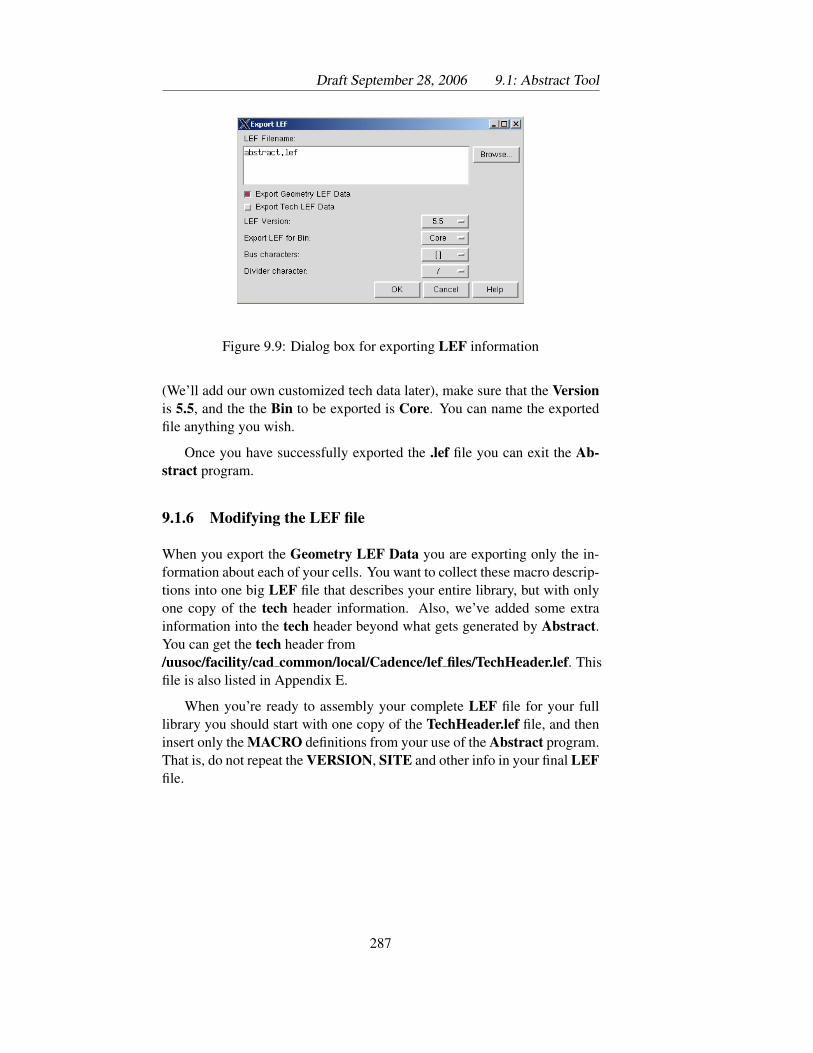
Draft September 28, 2006 9.1: Abstract Tool
Figure 9.9: Dialog box for exporting LEF information
(We’ll add our own customized tech data later), make sure that the Versionis 5.5, and the the Bin to be exported is Core. You can name the exportedfile anything you wish.
Once you have successfully exported the .lef file you can exit the Ab-stract program.
9.1.6 Modifying the LEF file
When you export the Geometry LEF Data you are exporting only the in-formation about each of your cells. You want to collect these macro descrip-tions into one big LEF file that describes your entire library, but with onlyone copy of the tech header information. Also, we’ve added some extrainformation into the tech header beyond what gets generated by Abstract.You can get the tech header from/uusoc/facility/cad common/local/Cadence/lef files/TechHeader.lef. Thisfile is also listed in Appendix E.
When you’re ready to assembly your complete LEF file for your fulllibrary you should start with one copy of the TechHeader.lef file, and theninsert only the MACRO definitions from your use of the Abstract program.That is, do not repeat the VERSION, SITE and other info in your final LEFfile.
287

CHAPTER 9: Abstract Generation Draft September 28, 2006
288
Chapter 10
SOC EncounterPlace and Route
PLACE AND ROUTE is the process of taking a structural file (Verilogin our case) and making a physical chip from that description. Itinvolves placing the cells on the chip, and routing the wiring con-
nections between those cells. The structural Verilog file gives all the in-formation about the circuit that should be assembled. It is simply a list ofstandard cells and the connections between those cells. The cell layouts areused to place the cells physically on the chip. More accurately, the abstractviews of the cells are used. The abstracts have only information about theconnection points of the cells (the pins), and routing obstructions in thosecells. Obstructions are simply layers of material in the cell that conflict withthe layers that the routing tool wants to use for making the connections. Es-sentially it is a layout view of the cell that is restricted to pins and metalrouting layers. This reduces the amount of information that’s required bythe place and route tool, and it also lets the vendor of the cells to keep otherdetails of their cells (like transistor information) private. It’s not need forplace and route, so it’s not included in the abstract view.
The files required before starting place and route are:
Cell characterization data: This should be in a liberty (or <filename>.lib)formatted file. It is the detailed timing, power, and functionality infor-mation that you derived through the characterization process (Chap-ter 7). It’s possible that you might have up to three different .lib fileswith typ, worst, and best timing, but you can complete the processwith only a single .lib file. It is very important that your .lib file in-clude footprints for all cells. In particular you will need to know thefootprint of inverter, buffer, and delay cells (delay cells can just bebuffers or inverters). If you have special buffers/inverters for building
CHAPTER 10: SOC EncounterPlace and Route Draft October 16, 2006
clock trees, those should use a different footprint than the “regular”buffers and inverters. If you have multiple drive strengths of any cellswith the same functionality, those cells should have the same foot-print. This enables certain timing optimizations in the place and routetool.
You might have multiple .lib files if your structural Verilog uses cellsfrom multiple libraries.
Cell abstract information: This is information that you generated throughthe abstract process (Chapter 9), and is contained in a LEF (or <filename>.lef)file. The LEF file should include technology information and macroinformation about all the cells in your library.
You might have multiple .lef files if your structural Verilog uses cellsfrom multiple different libraries.
Structural Verilog: This file defines the circuit that you want to have as-sembled by the place and route tool. It should be a purely structuraldescription that contains nothing but instantiations of cells from yourlibrary or libraries.
If your design is hierarchical you might have multiple Verilog filesthat describe the complete design. That is, some Verilog modulesmight include instantiations of other modules in addition to just cells.In any case you should know the name of the top-level module that isthe circuit that you want to place and route.
Delay constraint information: This is used by the place and router dur-ing timing optimization and clock tree generation. It describes thetiming and loading of primary inputs and outputs. It also defines theclock signal and the required timing of the clock signal. This filewill have been generated by the Synopsys synthesis process, and is<filename>.sdc. You can also generate this by hand since it’s just atext file, but it’s much easier to let Synopsys generate this file based onthe timing constraints you specified as part of the synthesis procedure(Chapter 8).
If you have all these files you can proceed to use the place and routetool to assemble that circuit on a chip. In our case we’ll be using the SOCEncounter tool from Cadence. My recommendation is to make a newdirectory from which to run the tool. I’ll make an IC CAD/soc direc-tory, and in fact, under that I’ll usually make distinct directories for eachproject I’m running through the soc tool. In this example I’ll be using asimple counter that is synthesized from the behavioral Verilog code in Fig-ure 10.1 so I’ll make an IC CAD/soc/count directory to run this ex-ample. Inside this directory I’ll make copies or links to the .lib and .lef
292
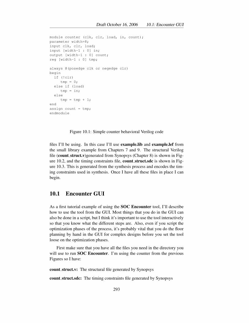
Draft October 16, 2006 10.1: Encounter GUI
module counter (clk, clr, load, in, count);parameter width=8;input clk, clr, load;input [width-1 : 0] in;output [width-1 : 0] count;reg [width-1 : 0] tmp;
always @(posedge clk or negedge clr)beginif (!clr)
tmp = 0;else if (load)
tmp = in;else
tmp = tmp + 1;endassign count = tmp;endmodule
Figure 10.1: Simple counter behavioral Verilog code
files I’ll be using. In this case I’ll use example.lib and example.lef fromthe small library example from Chapters 7 and 9. The structural Verilogfile (count struct.v)generated from Synopsys (Chapter 8) is shown in Fig-ure 10.2, and the timing constraints file, count struct.sdc is shown in Fig-ure 10.3. This is generated from the synthesis process and encodes the tim-ing constraints used in synthesis. Once I have all these files in place I canbegin.
10.1 Encounter GUI
As a first tutorial example of using the SOC Encounter tool, I’ll describehow to use the tool from the GUI. Most things that you do in the GUI canalso be done in a script, but I think it’s important to use the tool interactivelyso that you know what the different steps are. Also, even if you script theoptimization phases of the process, it’s probably vital that you do the floorplanning by hand in the GUI for complex designs before you set the toolloose on the optimization phases.
First make sure that you have all the files you need in the directory youwill use to run SOC Encounter. I’m using the counter from the previousFigures so I have:
count struct.v: The structural file generated by Synopsys
count struct.sdc: The timing constraints file generated by Synopsys
293
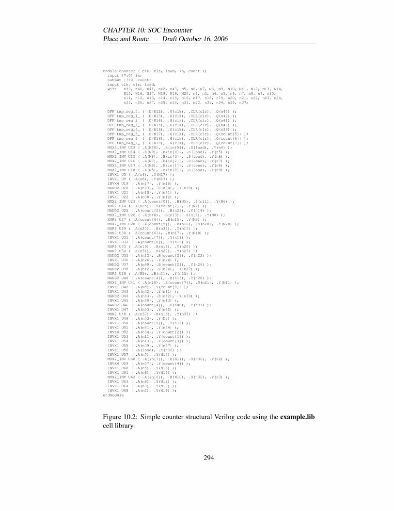
CHAPTER 10: SOC EncounterPlace and Route Draft October 16, 2006
module counter ( clk, clr, load, in, count );input [7:0] in;output [7:0] count;input clk, clr, load;wire n39, n40, n41, n42, n43, N5, N6, N7, N8, N9, N10, N11, N12, N13, N14,
N15, N16, N17, N18, N19, N20, n2, n3, n4, n5, n6, n7, n8, n9, n10,n11, n12, n13, n14, n15, n16, n17, n18, n19, n20, n21, n22, n23, n24,n25, n26, n27, n28, n30, n31, n32, n33, n34, n36, n37;
DFF tmp_reg_0_ ( .D(N12), .G(clk), .CLR(clr), .Q(n43) );DFF tmp_reg_1_ ( .D(N13), .G(clk), .CLR(clr), .Q(n42) );DFF tmp_reg_2_ ( .D(N14), .G(clk), .CLR(clr), .Q(n41) );DFF tmp_reg_3_ ( .D(N15), .G(clk), .CLR(clr), .Q(n40) );DFF tmp_reg_4_ ( .D(N16), .G(clk), .CLR(clr), .Q(n39) );DFF tmp_reg_5_ ( .D(N17), .G(clk), .CLR(clr), .Q(count[5]) );DFF tmp_reg_6_ ( .D(N18), .G(clk), .CLR(clr), .Q(count[6]) );DFF tmp_reg_7_ ( .D(N19), .G(clk), .CLR(clr), .Q(count[7]) );MUX2_INV U13 ( .A(N20), .B(in[5]), .S(load), .Y(n4) );MUX2_INV U14 ( .A(N9), .B(in[4]), .S(load), .Y(n5) );MUX2_INV U15 ( .A(N8), .B(in[3]), .S(load), .Y(n6) );MUX2_INV U16 ( .A(N7), .B(in[2]), .S(load), .Y(n7) );MUX2_INV U17 ( .A(N6), .B(in[1]), .S(load), .Y(n8) );MUX2_INV U18 ( .A(N5), .B(in[0]), .S(load), .Y(n9) );INVX1 U5 ( .A(n4), .Y(N17) );INVX1 U9 ( .A(n8), .Y(N13) );INVX4 U19 ( .A(n27), .Y(n15) );NAND2 U20 ( .A(n23), .B(n20), .Y(n10) );INVX1 U21 ( .A(n10), .Y(n21) );INVX1 U22 ( .A(n30), .Y(n12) );MUX2_INV U23 ( .A(count[0]), .B(N5), .S(n11), .Y(N6) );XOR2 U24 ( .A(n25), .B(count[2]), .Y(N7) );NAND2 U25 ( .A(count[2]), .B(n25), .Y(n14) );MUX2_INV U26 ( .A(n40), .B(n13), .S(n14), .Y(N8) );XOR2 U27 ( .A(count[4]), .B(n15), .Y(N9) );MUX2_INV U28 ( .A(count[5]), .B(n16), .S(n28), .Y(N20) );NOR2 U29 ( .A(n27), .B(n32), .Y(n17) );XOR2 U30 ( .A(count[6]), .B(n17), .Y(N10) );INVX1 U31 ( .A(count[7]), .Y(n18) );INVX1 U32 ( .A(count[6]), .Y(n19) );NOR2 U33 ( .A(n19), .B(n16), .Y(n20) );NOR2 U34 ( .A(n31), .B(n22), .Y(n23) );NAND2 U35 ( .A(n12), .B(count[2]), .Y(n22) );INVX1 U36 ( .A(n26), .Y(n24) );NAND2 U37 ( .A(n40), .B(count[2]), .Y(n26) );NAND2 U38 ( .A(n12), .B(n24), .Y(n27) );NOR2 U39 ( .A(N5), .B(n11), .Y(n25) );NAND2 U40 ( .A(count[4]), .B(n15), .Y(n28) );MUX2_INV U41 ( .A(n18), .B(count[7]), .S(n21), .Y(N11) );INVX1 U42 ( .A(N5), .Y(count[0]) );INVX1 U43 ( .A(n42), .Y(n11) );NAND2 U44 ( .A(n43), .B(n42), .Y(n30) );INVX1 U45 ( .A(n40), .Y(n13) );NAND2 U46 ( .A(count[4]), .B(n40), .Y(n31) );INVX1 U47 ( .A(n33), .Y(n32) );NOR2 U48 ( .A(n37), .B(n16), .Y(n33) );INVX1 U49 ( .A(n43), .Y(N5) );INVX1 U50 ( .A(count[5]), .Y(n16) );INVX1 U51 ( .A(n41), .Y(n34) );INVX4 U52 ( .A(n34), .Y(count[2]) );INVX1 U53 ( .A(n11), .Y(count[1]) );INVX1 U54 ( .A(n13), .Y(count[3]) );INVX1 U55 ( .A(n39), .Y(n37) );INVX1 U56 ( .A(load), .Y(n36) );INVX1 U57 ( .A(n7), .Y(N14) );MUX2_INV U58 ( .A(in[7]), .B(N11), .S(n36), .Y(n2) );INVX4 U59 ( .A(n37), .Y(count[4]) );INVX1 U60 ( .A(n5), .Y(N16) );INVX1 U61 ( .A(n6), .Y(N15) );MUX2_INV U62 ( .A(in[6]), .B(N10), .S(n36), .Y(n3) );INVX1 U63 ( .A(n9), .Y(N12) );INVX1 U64 ( .A(n3), .Y(N18) );INVX1 U65 ( .A(n2), .Y(N19) );
endmodule
Figure 10.2: Simple counter structural Verilog code using the example.libcell library
294
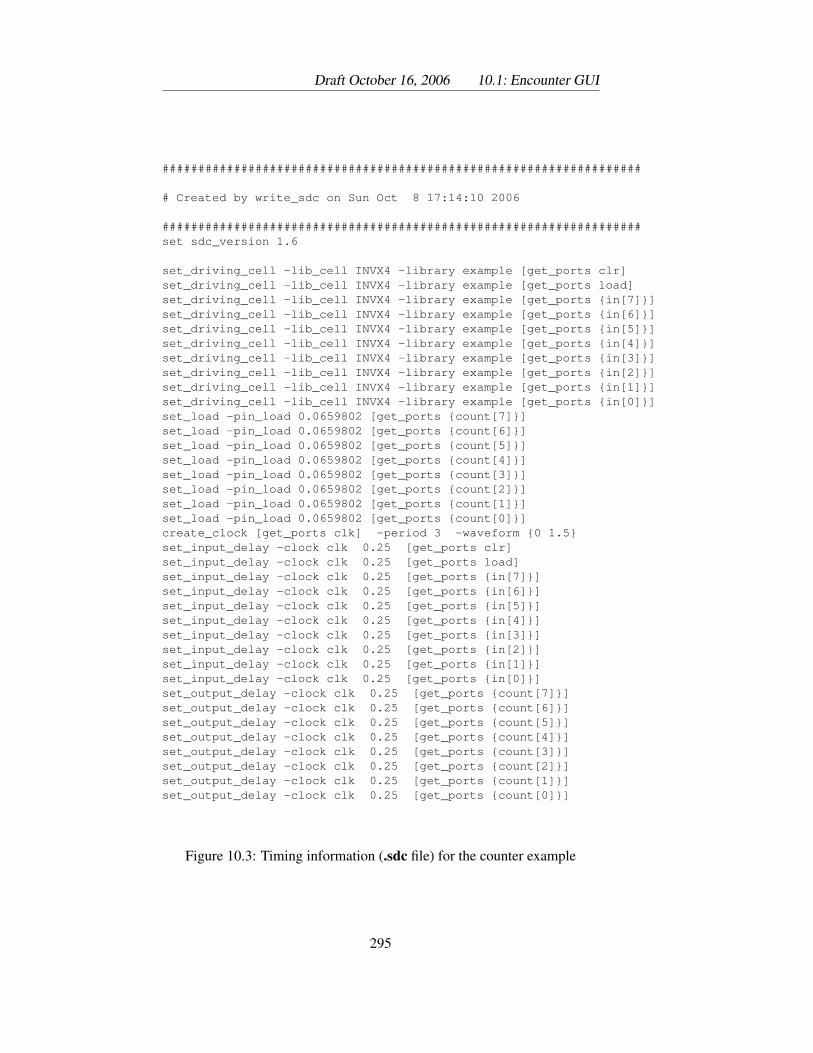
Draft October 16, 2006 10.1: Encounter GUI
###################################################################
# Created by write_sdc on Sun Oct 8 17:14:10 2006
###################################################################set sdc_version 1.6
set_driving_cell -lib_cell INVX4 -library example [get_ports clr]set_driving_cell -lib_cell INVX4 -library example [get_ports load]set_driving_cell -lib_cell INVX4 -library example [get_ports {in[7]}]set_driving_cell -lib_cell INVX4 -library example [get_ports {in[6]}]set_driving_cell -lib_cell INVX4 -library example [get_ports {in[5]}]set_driving_cell -lib_cell INVX4 -library example [get_ports {in[4]}]set_driving_cell -lib_cell INVX4 -library example [get_ports {in[3]}]set_driving_cell -lib_cell INVX4 -library example [get_ports {in[2]}]set_driving_cell -lib_cell INVX4 -library example [get_ports {in[1]}]set_driving_cell -lib_cell INVX4 -library example [get_ports {in[0]}]set_load -pin_load 0.0659802 [get_ports {count[7]}]set_load -pin_load 0.0659802 [get_ports {count[6]}]set_load -pin_load 0.0659802 [get_ports {count[5]}]set_load -pin_load 0.0659802 [get_ports {count[4]}]set_load -pin_load 0.0659802 [get_ports {count[3]}]set_load -pin_load 0.0659802 [get_ports {count[2]}]set_load -pin_load 0.0659802 [get_ports {count[1]}]set_load -pin_load 0.0659802 [get_ports {count[0]}]create_clock [get_ports clk] -period 3 -waveform {0 1.5}set_input_delay -clock clk 0.25 [get_ports clr]set_input_delay -clock clk 0.25 [get_ports load]set_input_delay -clock clk 0.25 [get_ports {in[7]}]set_input_delay -clock clk 0.25 [get_ports {in[6]}]set_input_delay -clock clk 0.25 [get_ports {in[5]}]set_input_delay -clock clk 0.25 [get_ports {in[4]}]set_input_delay -clock clk 0.25 [get_ports {in[3]}]set_input_delay -clock clk 0.25 [get_ports {in[2]}]set_input_delay -clock clk 0.25 [get_ports {in[1]}]set_input_delay -clock clk 0.25 [get_ports {in[0]}]set_output_delay -clock clk 0.25 [get_ports {count[7]}]set_output_delay -clock clk 0.25 [get_ports {count[6]}]set_output_delay -clock clk 0.25 [get_ports {count[5]}]set_output_delay -clock clk 0.25 [get_ports {count[4]}]set_output_delay -clock clk 0.25 [get_ports {count[3]}]set_output_delay -clock clk 0.25 [get_ports {count[2]}]set_output_delay -clock clk 0.25 [get_ports {count[1]}]set_output_delay -clock clk 0.25 [get_ports {count[0]}]
Figure 10.3: Timing information (.sdc file) for the counter example
295
CHAPTER 10: SOC EncounterPlace and Route Draft October 16, 2006
example.lib: A link to my cell library’s characterized data in .lib format.Make sure this file has footprint information for all cells.
example.lef: A link to my cell library’s abstract data in .lef form. Makesure that you have correctly appended the TechHeader.lef informa-tion in front of the MACRO definitions.
After connecting to your directory (I’m using IC CAD/soc/counter)you can start the SOC Encounter tool using the cad-soc script. You’llsee the main encounter window as seen in Figure 10.4. This Figure isannotated to describe the different areas of the screen. The pallete on theright lets you choose what is currently visible in the design display area.The Design Views change how you see that design. From left to right theDesign Views are:
Floorplan View: This view shows the overall floorplan of your chip. Itlets you see the area that is generated for the standard cells, and howthe different pieces of your design hierarchy fit into that standard cellarea. For this first example there is no hierarchy in the design so theentire counter will be placed inside the cell area. For a more complexdesign you can manually place the different pieces of the design inthe cell area if you wish.
Amoeba View: This view shows information related to the Amoeba place-ment and routing of the cells. It gives feedback on cell placement,density, and congestion.
Physical View: This view shows the actual cells as they are placed, and theactual wires as they are routed by the tool.
All three views are useful, but I generally start out with the floorplanview during, as you might guess, floorplanning, then toggle between the thatview and the physical view once the place and route gets under way.
10.1.1 Reading in the Design
Once the tool is started you need to read all your design files into the tool.Select the Design → Design Import... menu choice to get the Design Im-port dialog box. This box has multiple fields in multiple tabs that you needto fill in. First fill in the Basic fields with the following (see Figure 10.5):
Verilog Netlist: Your structural Verilog file or files. You can either let SOCEncounter pick the top cell, or you can provide the name of the toplevel module.
296
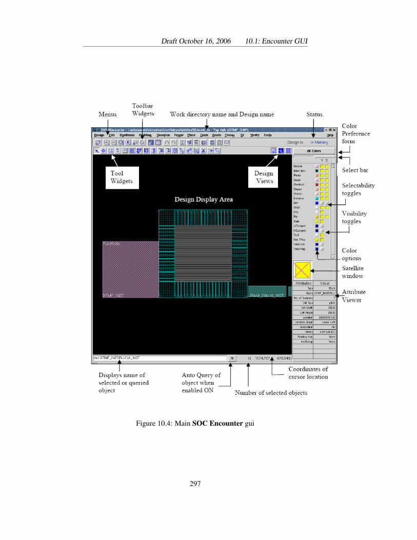
Draft October 16, 2006 10.1: Encounter GUI
Figure 10.4: Main SOC Encounter gui
297
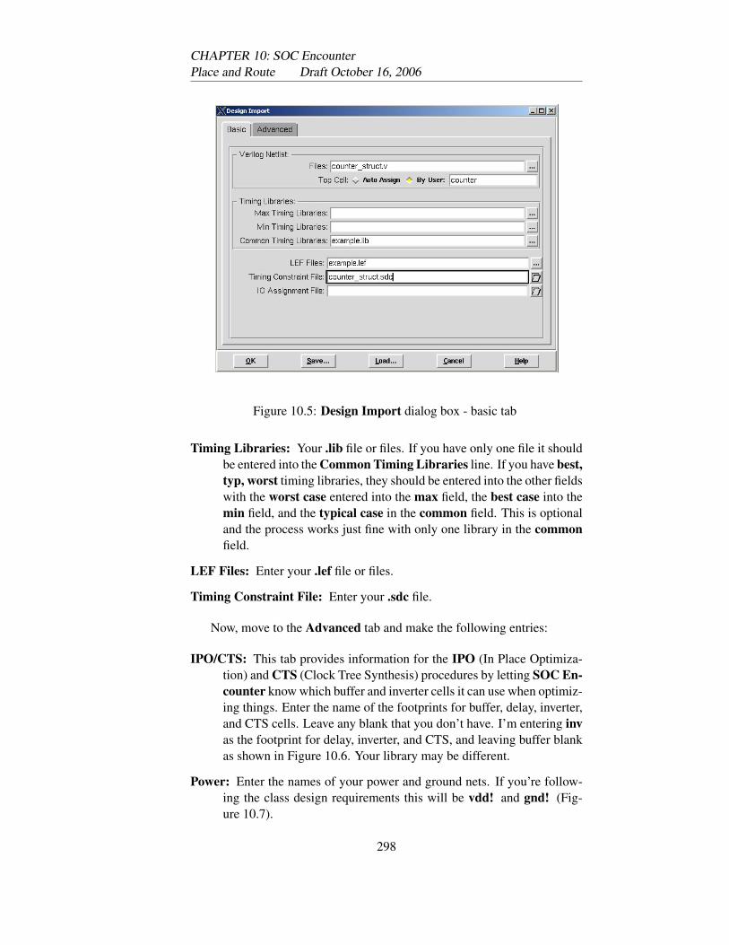
CHAPTER 10: SOC EncounterPlace and Route Draft October 16, 2006
Figure 10.5: Design Import dialog box - basic tab
Timing Libraries: Your .lib file or files. If you have only one file it shouldbe entered into the Common Timing Libraries line. If you have best,typ, worst timing libraries, they should be entered into the other fieldswith the worst case entered into the max field, the best case into themin field, and the typical case in the common field. This is optionaland the process works just fine with only one library in the commonfield.
LEF Files: Enter your .lef file or files.
Timing Constraint File: Enter your .sdc file.
Now, move to the Advanced tab and make the following entries:
IPO/CTS: This tab provides information for the IPO (In Place Optimiza-tion) and CTS (Clock Tree Synthesis) procedures by letting SOC En-counter know which buffer and inverter cells it can use when optimiz-ing things. Enter the name of the footprints for buffer, delay, inverter,and CTS cells. Leave any blank that you don’t have. I’m entering invas the footprint for delay, inverter, and CTS, and leaving buffer blankas shown in Figure 10.6. Your library may be different.
Power: Enter the names of your power and ground nets. If you’re follow-ing the class design requirements this will be vdd! and gnd! (Fig-ure 10.7).
298
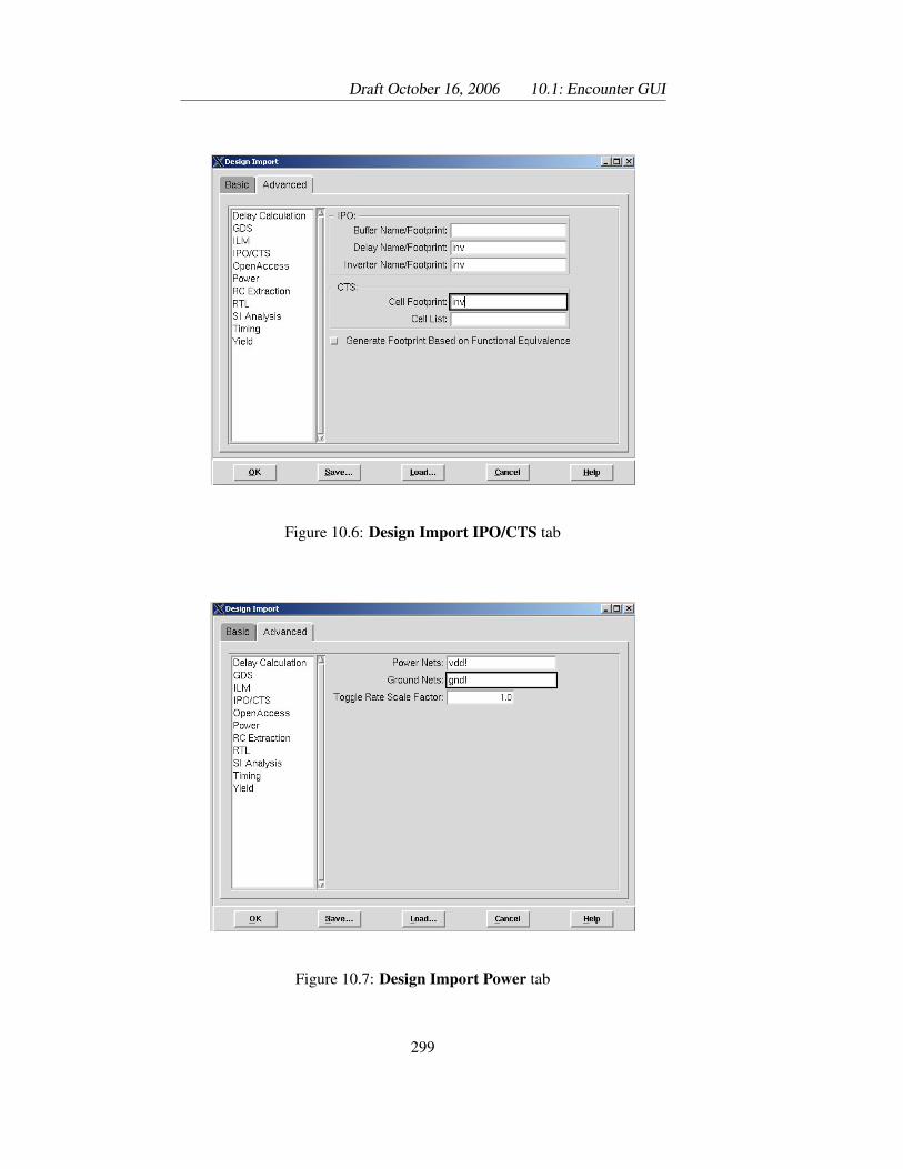
Draft October 16, 2006 10.1: Encounter GUI
Figure 10.6: Design Import IPO/CTS tab
Figure 10.7: Design Import Power tab
299
CHAPTER 10: SOC EncounterPlace and Route Draft October 16, 2006
Now you can press OK and read all this information into SOC En-counter. The comments (and potential warnings and errors) will show upin the shell window in which you invoked cad-soc . You should look atthem carefully to make sure that things have imported correctly. If they didyou will see the SOC Encounter window has been updated to show a set ofrows in which standard cells will be placed.
10.1.2 Floorplanning
Floorplanning is the step where you make decisions about how denselypacked the standard cells will be, and how the large pieces of your designwill be placed relative to each other. Because there is only one top-levelmodule in the counter example, this is automatically assumed to cover theentire standard cell area. If your design had mode structure in terms of hi-erarchical modules, those modules would be placed to the side of the cellplacement area so that you could place them as desired inside the cell area.The default is just to let the entire top-level design fill the standard cell areawithout further structuring. In practice this spreads out the entire designacross the entire area which, for large systems with significant structure,may result in lower performance. For a system with significant structure acareful placement of the major blocks can have a dramatic impact on systemperformance.
But, for this example, what we really care about is cell density and otherarea parameters related to the design. Select Floorplan → Specify Floor-plan... to get the floorplanning dialog box (Figure 10.8). In this dialog boxyou can change various parameters related to the floorplan:
Aspect Ratio: This sets the (rectangular) shape of the cell. An aspect ofclose to 1 is close to square. An aspect of .5 is a rectangle with thevertical edge half as long as the horizontal, and 1.5 is a rectangle withthe vertical edge twice the horizontal. This is handy if you’re tryingto make a subsystem to fit in a larger project. For now, just for fun,I’ll change the aspect ratio to 0.5. Note that the tool will adjust thisnumber a little based on the anticipated cell sizes.
Core Utilization: This lets the tool know how densely packed the coreshould be with standard cells. The default is around 70% which leavesroom for in place optimization and clock tree synthesis, both ofwhich may add extra cells during their operation. For a large complexdesign you may even have to reduce the utilization percentage belowthis.
Core Margins: These should be set by Core to IO Boundary and areAll measurements areassumed to be in
microns. 300
Draft October 16, 2006 10.1: Encounter GUI
to leave room for the power and ground rings that will be generatedaround your cell. All the Core to ... values should be set to 30. Notethat even though you specify 30, when you apply those values theymay change slightly according to SOC Encounter’s measurements.
Others: Other spots in the Specify Floorplan dialog can be left as de-fault. In particular you want the standard cell rows to be Double-backRows, and you can leave the Row Spacing as zero to leave no spacebetween the rows. If your design proves hard to route you can startagain and leave extra space between the rows for routing.
After adjusting the floorplan, the main SOC Encounter window lookslike Figure 10.9. The rows in which cells will be placed are in the centerwith the little corner diagonals showing how the cells in those rows willbe flipped. The dotted line is the outer dimension of the final cell. Thepower and ground rings will go in the space between the cells and the outerboundary.
Saving the Design
This is a good spot in which to save the current design. There are lots of I like to save the designat each major step sothat I can go back if Ineed to try somethingdifferent at that step. Beaware that there’s nogeneral “undo” functionin Encounter.
steps in the process that are not “undo-able.” It’s nice to save the design atvarious points so that if you want to try something different you can reloadthe design and try other things. Save the design with Design → Save De-sign... and name the saved file <filename>.enc. In my case I’ll name itfloorplan.enc so that I can restore to the point where I have a floorplan if Iwant to start over from this point. Saved designs are restored into the toolusing the Design → Restore Design... menu.
10.1.3 Power Planning
Now it’s time to put the power and ground ring around your circuit, andconnect that ring to the rows so that your cells will be connected to powerand ground when they’re placed in the row. Start with Power → PowerPlanning → Add Rings. From this dialog box (Figure 10.10) you cancontrol how the power rings are generated. The fields of interest are: Remember that all the
sizes and spacings youspecify must be divisibleby the basic lambda unitof our underlyingtechnology. That is,everything is measuredin units of 0.3 microns,so values should bedivisible by 0.3.
Ring Type: The defaults are good here. You should have the Core ring(s)contouring: set to Around core boundary.
Ring Configuration: You can select the metal layers you want to use forthe ring, their width, and their spacing. I’m making the top andbottom of the ring horizontal metal1, and the right and left vertical
301
CHAPTER 10: SOC EncounterPlace and Route Draft October 16, 2006
Figure 10.8: The Specify Floorplan dialog box
302
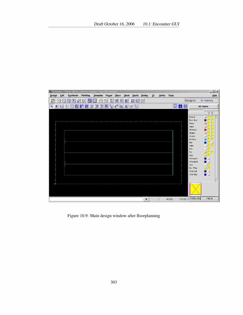
Draft October 16, 2006 10.1: Encounter GUI
Figure 10.9: Main design window after floorplanning
303
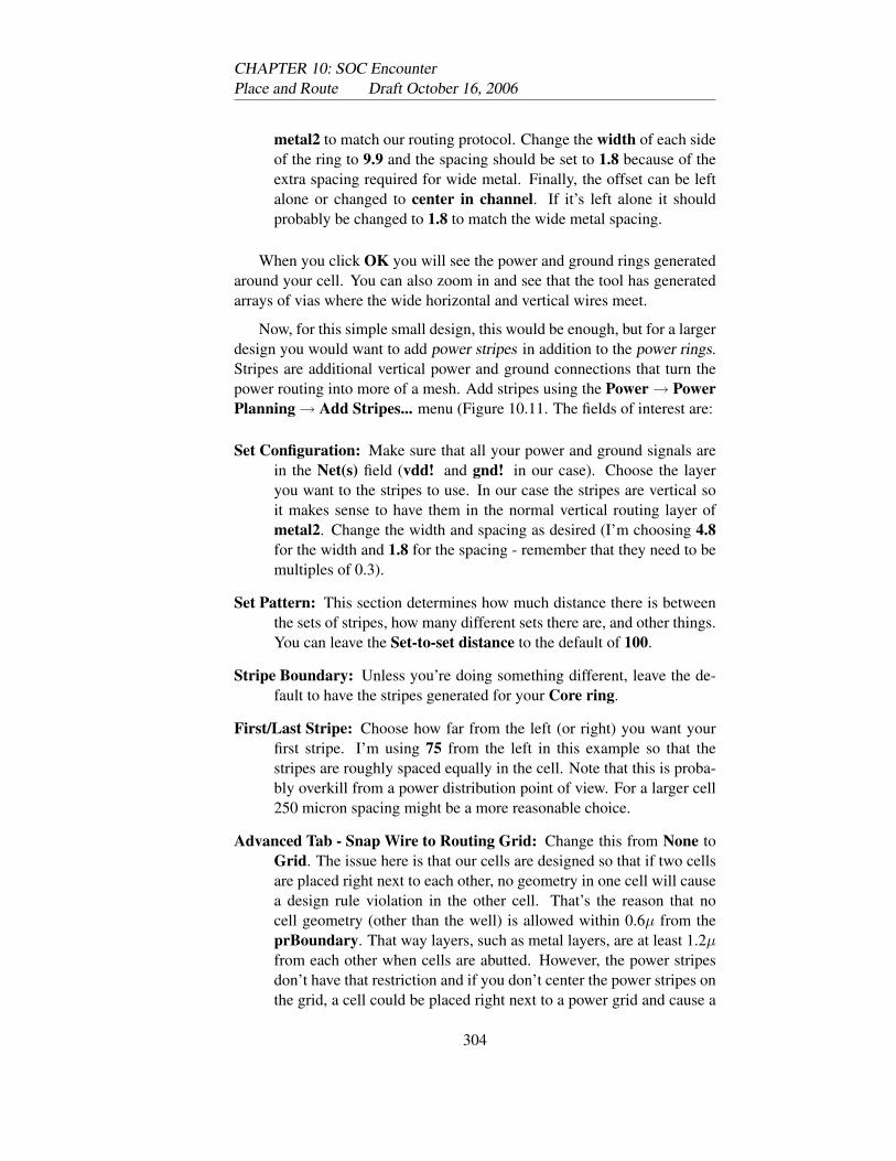
CHAPTER 10: SOC EncounterPlace and Route Draft October 16, 2006
metal2 to match our routing protocol. Change the width of each sideof the ring to 9.9 and the spacing should be set to 1.8 because of theextra spacing required for wide metal. Finally, the offset can be leftalone or changed to center in channel. If it’s left alone it shouldprobably be changed to 1.8 to match the wide metal spacing.
When you click OK you will see the power and ground rings generatedaround your cell. You can also zoom in and see that the tool has generatedarrays of vias where the wide horizontal and vertical wires meet.
Now, for this simple small design, this would be enough, but for a largerdesign you would want to add power stripes in addition to the power rings.Stripes are additional vertical power and ground connections that turn thepower routing into more of a mesh. Add stripes using the Power → PowerPlanning → Add Stripes... menu (Figure 10.11. The fields of interest are:
Set Configuration: Make sure that all your power and ground signals arein the Net(s) field (vdd! and gnd! in our case). Choose the layeryou want to the stripes to use. In our case the stripes are vertical soit makes sense to have them in the normal vertical routing layer ofmetal2. Change the width and spacing as desired (I’m choosing 4.8for the width and 1.8 for the spacing - remember that they need to bemultiples of 0.3).
Set Pattern: This section determines how much distance there is betweenthe sets of stripes, how many different sets there are, and other things.You can leave the Set-to-set distance to the default of 100.
Stripe Boundary: Unless you’re doing something different, leave the de-fault to have the stripes generated for your Core ring.
First/Last Stripe: Choose how far from the left (or right) you want yourfirst stripe. I’m using 75 from the left in this example so that thestripes are roughly spaced equally in the cell. Note that this is proba-bly overkill from a power distribution point of view. For a larger cell250 micron spacing might be a more reasonable choice.
Advanced Tab - Snap Wire to Routing Grid: Change this from None toGrid. The issue here is that our cells are designed so that if two cellsare placed right next to each other, no geometry in one cell will causea design rule violation in the other cell. That’s the reason that nocell geometry (other than the well) is allowed within 0.6µ from theprBoundary. That way layers, such as metal layers, are at least 1.2µfrom each other when cells are abutted. However, the power stripesdon’t have that restriction and if you don’t center the power stripes onthe grid, a cell could be placed right next to a power grid and cause a
304
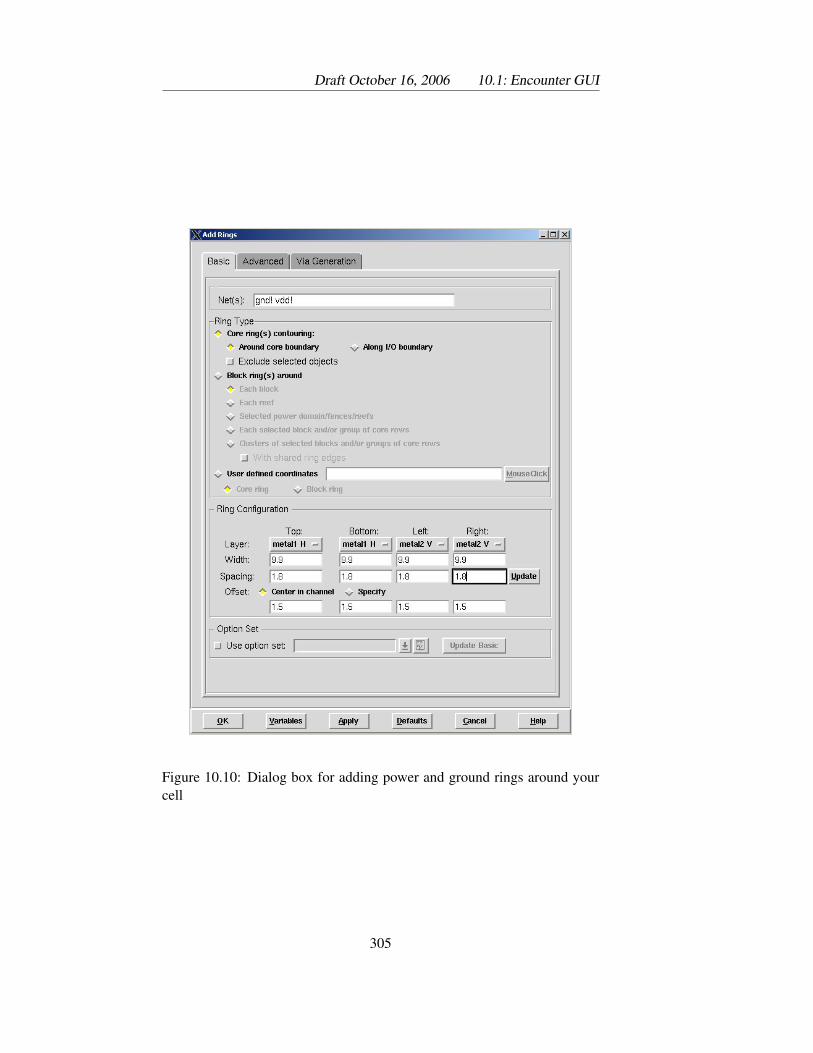
Draft October 16, 2006 10.1: Encounter GUI
Figure 10.10: Dialog box for adding power and ground rings around yourcell
305
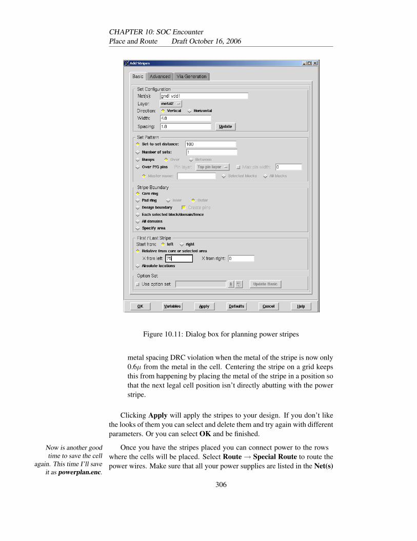
CHAPTER 10: SOC EncounterPlace and Route Draft October 16, 2006
Figure 10.11: Dialog box for planning power stripes
metal spacing DRC violation when the metal of the stripe is now only0.6µ from the metal in the cell. Centering the stripe on a grid keepsthis from happening by placing the metal of the stripe in a position sothat the next legal cell position isn’t directly abutting with the powerstripe.
Clicking Apply will apply the stripes to your design. If you don’t likethe looks of them you can select and delete them and try again with differentparameters. Or you can select OK and be finished.
Once you have the stripes placed you can connect power to the rowsNow is another goodtime to save the cell
again. This time I’ll saveit as powerplan.enc.
where the cells will be placed. Select Route → Special Route to route thepower wires. Make sure that all your power supplies are listed in the Net(s)
306
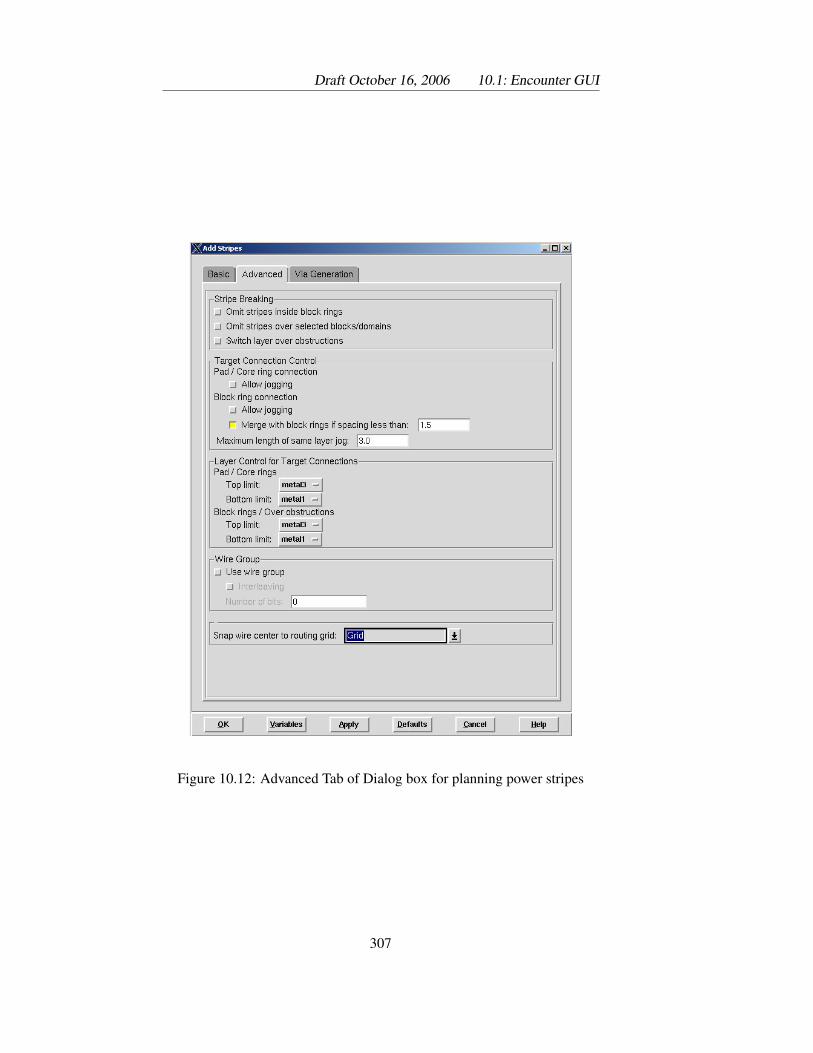
Draft October 16, 2006 10.1: Encounter GUI
Figure 10.12: Advanced Tab of Dialog box for planning power stripes
307
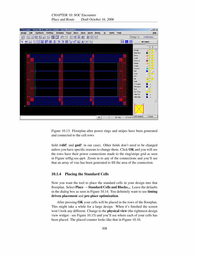
CHAPTER 10: SOC EncounterPlace and Route Draft October 16, 2006
Figure 10.13: Floorplan after power rings and stripes have been generatedand connected to the cell rows
field (vdd! and gnd! in our case). Other fields don’t need to be changedunless you have specific reasons to change them. Click OK and you will seethe rows have their power connections made to the ring/stripe grid as seenin Figure reffig:soc-pp4. Zoom in to any of the connections and you’ll seethat an array of vias has been generated to fill the area of the connection.
10.1.4 Placing the Standard Cells
Now you want the tool to place the standard cells in your design into thatfloorplan. Select Place→ Standard Cells and Blocks.... Leave the defaultsin the dialog box as seen in Figure 10.14. You definitely want to use timingdriven placement and pre-place optimization.
After pressing OK your cells will be placed in the rows of the floorplan.This might take a while for a large design. When it’s finished the screenwon’t look any different. Change to the physical view (the rightmost designview widget - see Figure 10.15) and you’ll see where each of your cells hasbeen placed. The placed counter looks like that in Figure 10.16.
308
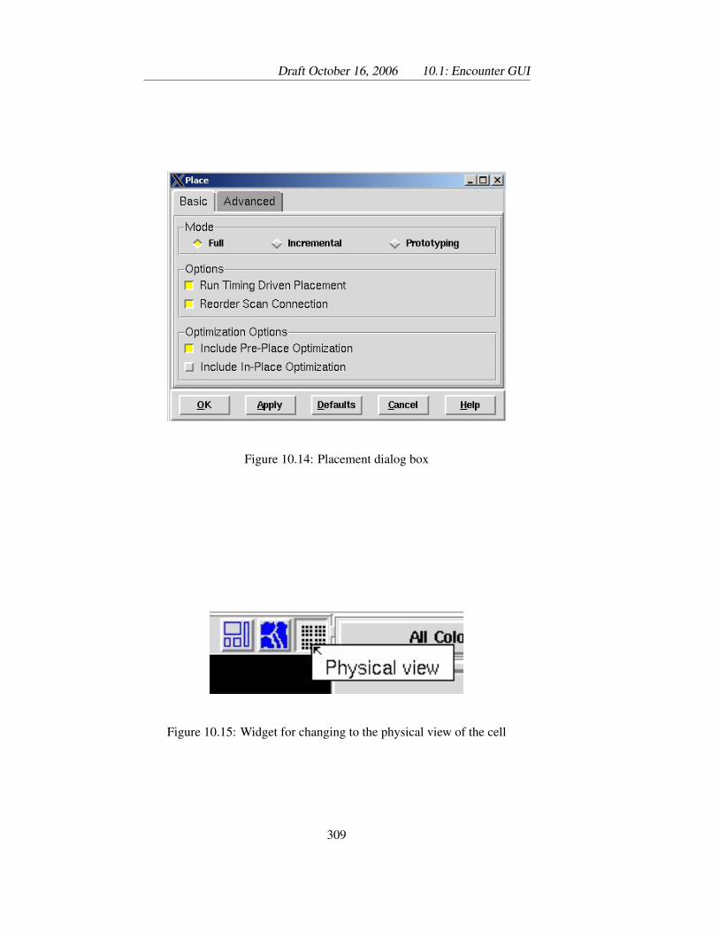
Draft October 16, 2006 10.1: Encounter GUI
Figure 10.14: Placement dialog box
Figure 10.15: Widget for changing to the physical view of the cell
309
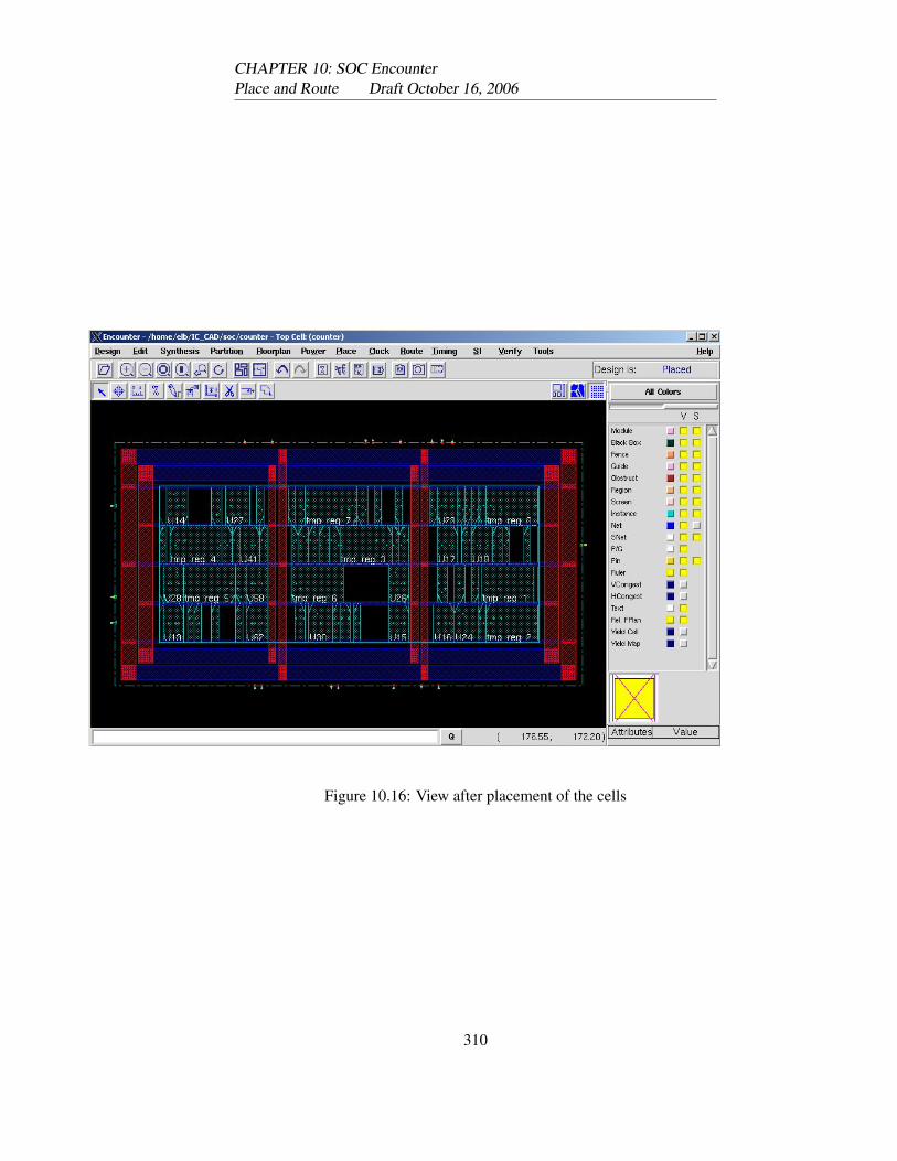
CHAPTER 10: SOC EncounterPlace and Route Draft October 16, 2006
Figure 10.16: View after placement of the cells
310
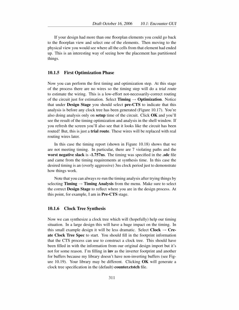
Draft October 16, 2006 10.1: Encounter GUI
If your design had more than one floorplan elements you could go backto the floorplan view and select one of the elements. Then moving to thephysical view you would see where all the cells from that element had endedup. This is an interesting way of seeing how the placement has partitionedthings.
10.1.5 First Optimization Phase
Now you can perform the first timing and optimization step. At this stageof the process there are no wires so the timing step will do a trial routeto estimate the wiring. This is a low-effort not-necessarily-correct routingof the circuit just for estimation. Select Timing → Optimization. Noticethat under Design Stage you should select pre-CTS to indicate that thisanalysis is before any clock tree has been generated (Figure 10.17). You’realso doing analysis only on setup time of the circuit. Click OK and you’llsee the result of the timing optimization and analysis in the shell window. Ifyou refresh the screen you’ll also see that it looks like the circuit has beenrouted! But, this is just a trial route. These wires will be replaced with realrouting wires later.
In this case the timing report (shown in Figure 10.18) shows that weare not meeting timing. In particular, there are 7 violating paths and theworst negative slack is -1.757ns. The timing was specified in the .sdc fileand came from the timing requirements at synthesis time. In this case thedesired timing is an (overly aggressive) 3ns clock period just to demonstratehow things work.
Note that you can always re-run the timing analysis after trying things byselecting Timing → Timing Analysis from the menu. Make sure to selectthe correct Design Stage to reflect where you are in the design process. Atthis point, for example, I am in Pre-CTS stage.
10.1.6 Clock Tree Synthesis
Now we can synthesize a clock tree which will (hopefully) help our timingsituation. In a large design this will have a huge impact on the timing. Inthis small example design it will be less dramatic. Select Clock → Cre-ate Clock Tree Spec to start. You should fill in the footprint informationthat the CTS process can use to construct a clock tree. This should havebeen filled in with the information from our original design import but it’snot for some reason. I’m filling in inv as the inverter footprint and anotherfor buffers because my library doesn’t have non-inverting buffers (see Fig-ure 10.19). Your library may be different. Clicking OK will generate aclock tree specification in the (default) counter.ctstch file.
311
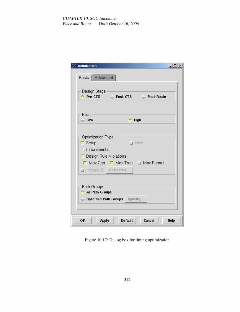
CHAPTER 10: SOC EncounterPlace and Route Draft October 16, 2006
Figure 10.17: Dialog box for timing optimization
312
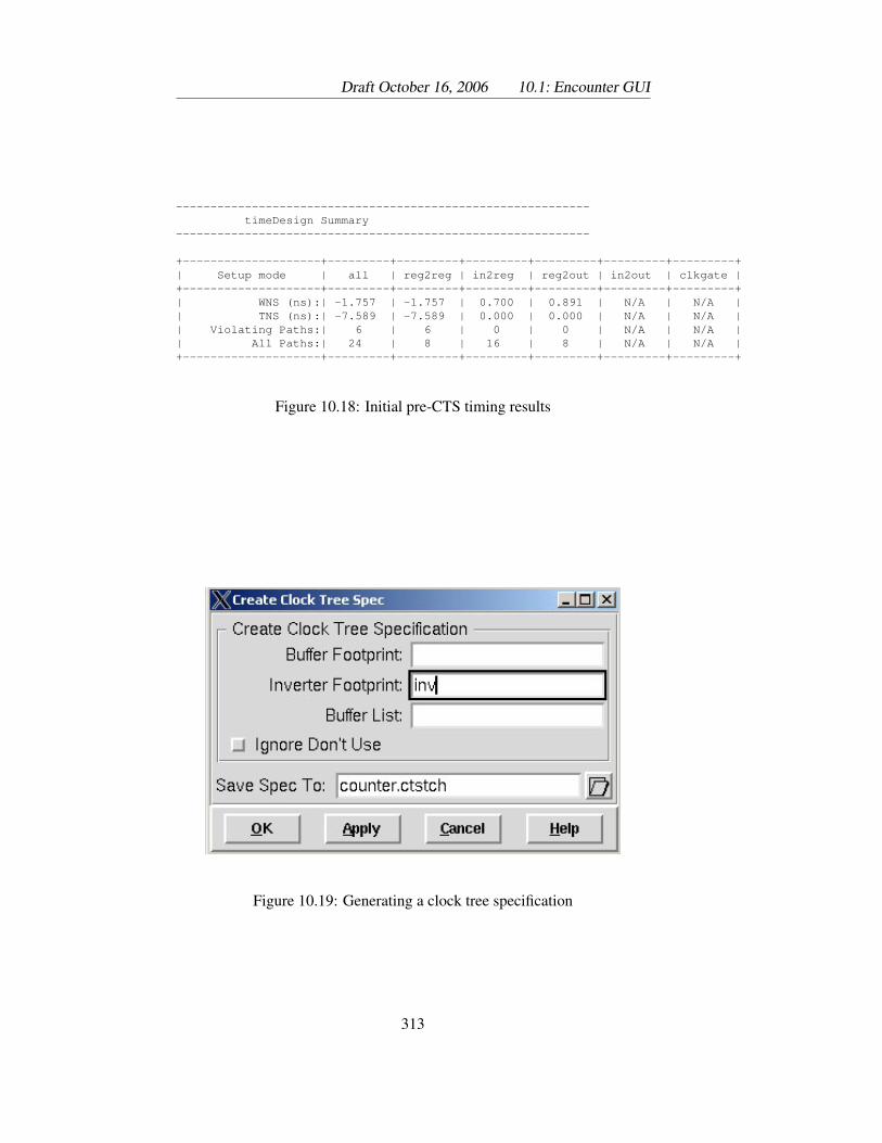
Draft October 16, 2006 10.1: Encounter GUI
------------------------------------------------------------timeDesign Summary
------------------------------------------------------------
+--------------------+---------+---------+---------+---------+---------+---------+| Setup mode | all | reg2reg | in2reg | reg2out | in2out | clkgate |+--------------------+---------+---------+---------+---------+---------+---------+| WNS (ns):| -1.757 | -1.757 | 0.700 | 0.891 | N/A | N/A || TNS (ns):| -7.589 | -7.589 | 0.000 | 0.000 | N/A | N/A || Violating Paths:| 6 | 6 | 0 | 0 | N/A | N/A || All Paths:| 24 | 8 | 16 | 8 | N/A | N/A |+--------------------+---------+---------+---------+---------+---------+---------+
Figure 10.18: Initial pre-CTS timing results
Figure 10.19: Generating a clock tree specification
313
CHAPTER 10: SOC EncounterPlace and Route Draft October 16, 2006
Now you need to specify the clock tree based on this spec (yes, thisseems a little redundant...). Select Clock → Specify Clock Tree and usethe clock tree specification file (counter.ctstch) that you just generated.
Now you can actually generate the clock tree with Clock→ SynthesizeClock Tree. You can leave the defaults in this dialog box and just click OKto generate the clock tree. This will use the cells you told it about to generatea clock tree in your circuit. If you watched carefully you would have seensome cells added and other cells moved around during this process.
If you’d like to see the clock tree that was generated you can selectClock→ Display→ Display Clock Tree to see the tree. This will annotatethe display to show the tree. You should select Clock Route Only in thedialog box (Figure 10.20). If you select Display Clock Phase Delay you’llsee the clock tree (in blue) and the flip flops connected to that tree coloredby their differing phase delays. If you select Display Min/Max Paths you’llsee the min and max path from the clock pin to the flip flop displayed. SeeFigure 10.21 for an example. You can clear the clock tree display withClock → Display → Clear Clock Tree Display.
10.1.7 Post-CTS Optimization
After you have generated the clock tree you can do another phase of timingoptimization. Again select Timing → Optimization but this time selectpost-CTS (refer back to Figure 10.17). This optimization phase shows thatthe addition of the clock tree and the subsequent optimization helped a little,but not much. In a larger design this would have a much more dramaticimpact. See Figure 10.22.
10.1.8 Final Routing
Now that the design has a clock tree you can perform final routing of thedesign. Select Route → NanoRoute → Route to invoke the router. ThereFor a large complex
design you may need togo all the way back to
the floorplanning stageand add more space
between rows for routingchannels. Because this
technology has onlythree routing layers, and
you have likely used alot of metal1 in yourcells, the chance for
routing congestion inlarge designs is high.
are lots of controls, but Timing Driven is probably the only one you need tochange from the default (see Figure 10.23). Of course, you are welcome toplay around with these controls to see what happens. Once you select Tim-ing Driven you can also adjust the Effort slider to tell the tool how mucheffort to spend on meeting timing and how much on reducing congestion.On a large, aggressive design you may need to try things are various settingsto get something you like. Because this is not un-doable, you should savethe circuit in a state just before routing so that you can restore to that statebefore trying different routing options.
This can take a long time on a large design. Check the shell window
314
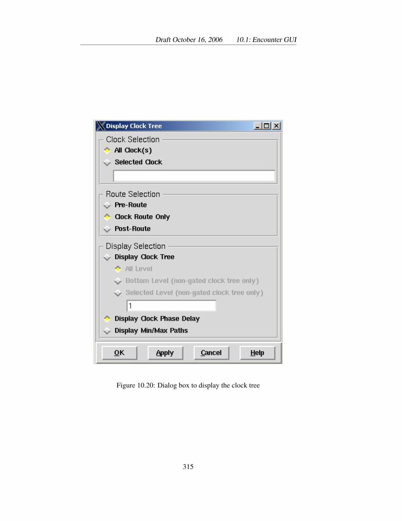
Draft October 16, 2006 10.1: Encounter GUI
Figure 10.20: Dialog box to display the clock tree
315
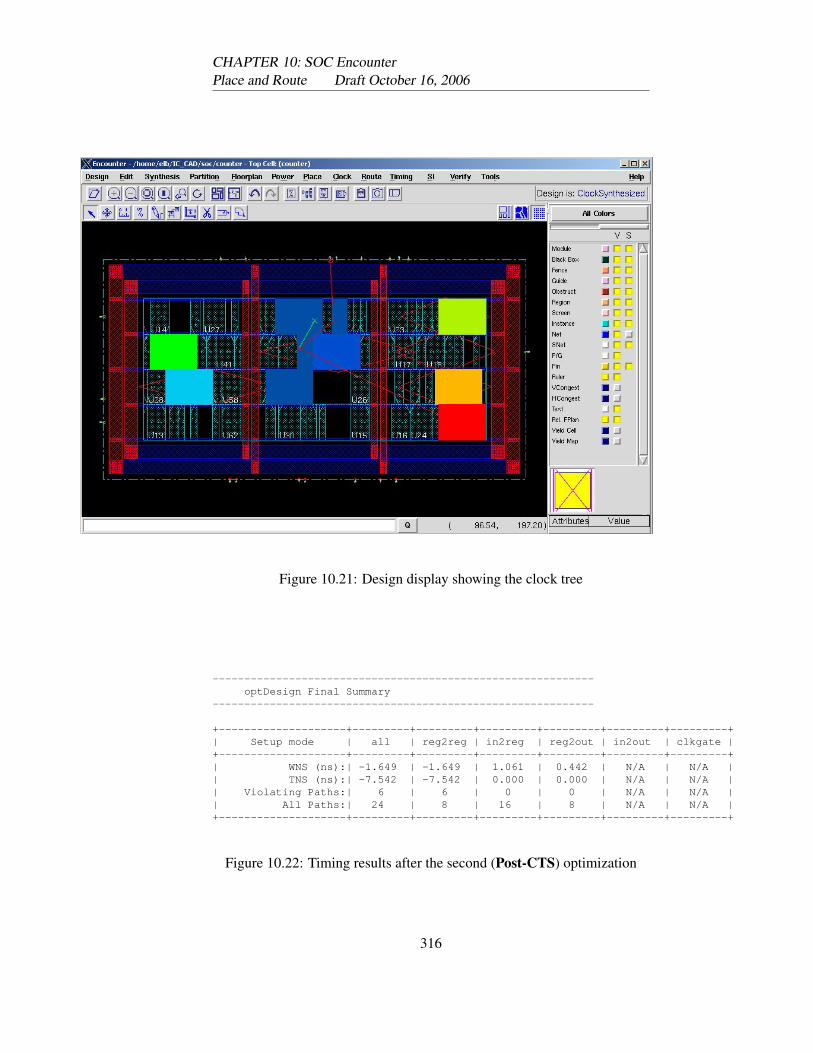
CHAPTER 10: SOC EncounterPlace and Route Draft October 16, 2006
Figure 10.21: Design display showing the clock tree
------------------------------------------------------------optDesign Final Summary
------------------------------------------------------------
+--------------------+---------+---------+---------+---------+---------+---------+| Setup mode | all | reg2reg | in2reg | reg2out | in2out | clkgate |+--------------------+---------+---------+---------+---------+---------+---------+| WNS (ns):| -1.649 | -1.649 | 1.061 | 0.442 | N/A | N/A || TNS (ns):| -7.542 | -7.542 | 0.000 | 0.000 | N/A | N/A || Violating Paths:| 6 | 6 | 0 | 0 | N/A | N/A || All Paths:| 24 | 8 | 16 | 8 | N/A | N/A |+--------------------+---------+---------+---------+---------+---------+---------+
Figure 10.22: Timing results after the second (Post-CTS) optimization
316
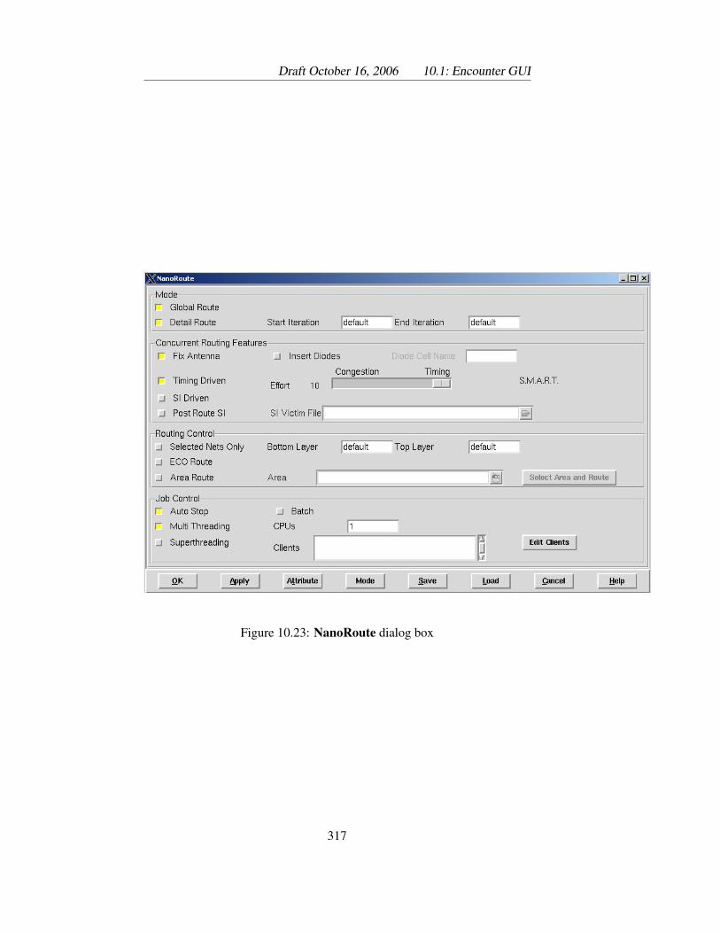
Draft October 16, 2006 10.1: Encounter GUI
Figure 10.23: NanoRoute dialog box
317
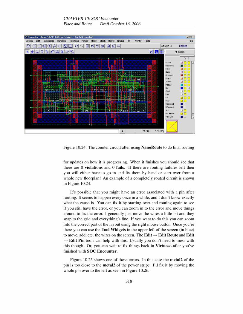
CHAPTER 10: SOC EncounterPlace and Route Draft October 16, 2006
Figure 10.24: The counter circuit after using NanoRoute to do final routing
for updates on how it is progressing. When it finishes you should see thatthere are 0 violations and 0 fails. If there are routing failures left thenyou will either have to go in and fix them by hand or start over from awhole new floorplan! An example of a completely routed circuit is shownin Figure 10.24.
It’s possible that you might have an error associated with a pin afterrouting. It seems to happen every once in a while, and I don’t know exactlywhat the cause is. You can fix it by starting over and routing again to seeif you still have the error, or you can zoom in to the error and move thingsaround to fix the error. I generally just move the wires a little bit and theysnap to the grid and everything’s fine. If you want to do this you can zoominto the correct part of the layout using the right mouse button. Once you’rethere you can use the Tool Widgets in the upper left of the screen (in blue)to move, add, etc. the wires on the screen. The Edit→ Edit Route and Edit→ Edit Pin tools can help with this. Usually you don’t need to mess withthis though. Or, you can wait to fix things back in Virtuoso after you’vefinished with SOC Encounter.
Figure 10.25 shows one of these errors. In this case the metal2 of thepin is too close to the metal2 of the power stripe. I’ll fix it by moving thewhole pin over to the left as seen in Figure 10.26.
318
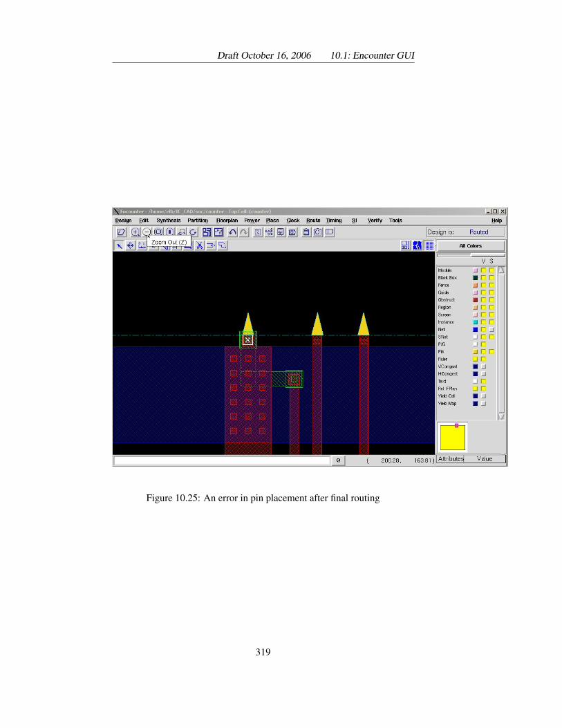
Draft October 16, 2006 10.1: Encounter GUI
Figure 10.25: An error in pin placement after final routing
319
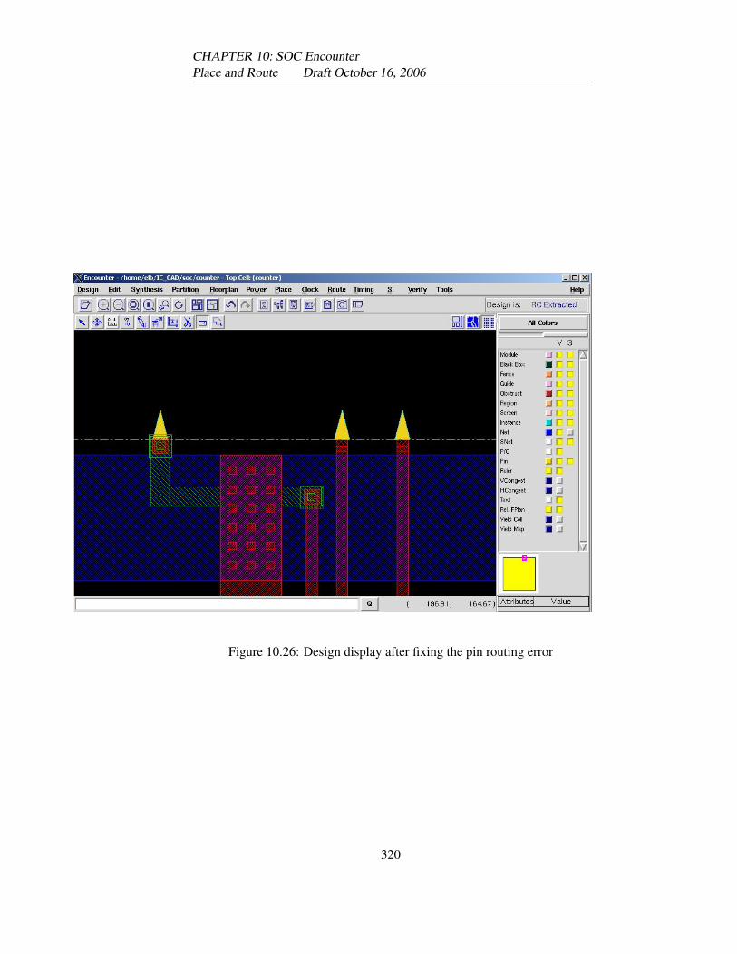
CHAPTER 10: SOC EncounterPlace and Route Draft October 16, 2006
Figure 10.26: Design display after fixing the pin routing error
320
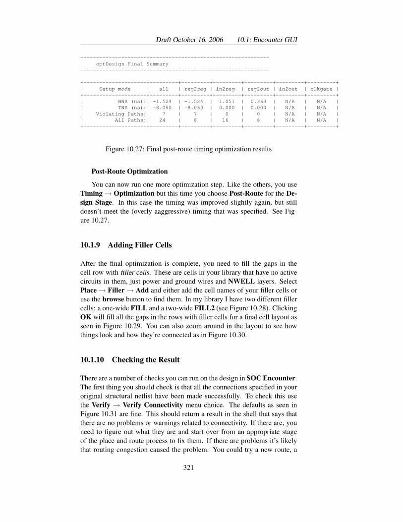
Draft October 16, 2006 10.1: Encounter GUI
------------------------------------------------------------optDesign Final Summary
------------------------------------------------------------
+--------------------+---------+---------+---------+---------+---------+---------+| Setup mode | all | reg2reg | in2reg | reg2out | in2out | clkgate |+--------------------+---------+---------+---------+---------+---------+---------+| WNS (ns):| -1.524 | -1.524 | 1.051 | 0.363 | N/A | N/A || TNS (ns):| -8.050 | -8.050 | 0.000 | 0.000 | N/A | N/A || Violating Paths:| 7 | 7 | 0 | 0 | N/A | N/A || All Paths:| 24 | 8 | 16 | 8 | N/A | N/A |+--------------------+---------+---------+---------+---------+---------+---------+
Figure 10.27: Final post-route timing optimization results
Post-Route Optimization
You can now run one more optimization step. Like the others, you useTiming → Optimization but this time you choose Post-Route for the De-sign Stage. In this case the timing was improved slightly again, but stilldoesn’t meet the (overly aaggressive) timing that was specified. See Fig-ure 10.27.
10.1.9 Adding Filler Cells
After the final optimization is complete, you need to fill the gaps in thecell row with filler cells. These are cells in your library that have no activecircuits in them, just power and ground wires and NWELL layers. SelectPlace → Filler → Add and either add the cell names of your filler cells oruse the browse button to find them. In my library I have two different fillercells: a one-wide FILL and a two-wide FILL2 (see Figure 10.28). ClickingOK will fill all the gaps in the rows with filler cells for a final cell layout asseen in Figure 10.29. You can also zoom around in the layout to see howthings look and how they’re connected as in Figure 10.30.
10.1.10 Checking the Result
There are a number of checks you can run on the design in SOC Encounter.The first thing you should check is that all the connections specified in youroriginal structural netlist have been made successfully. To check this usethe Verify → Verify Connectivity menu choice. The defaults as seen inFigure 10.31 are fine. This should return a result in the shell that says thatthere are no problems or warnings related to connectivity. If there are, youneed to figure out what they are and start over from an appropriate stageof the place and route process to fix them. If there are problems it’s likelythat routing congestion caused the problem. You could try a new route, a
321
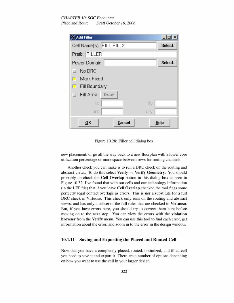
CHAPTER 10: SOC EncounterPlace and Route Draft October 16, 2006
Figure 10.28: Filler cell dialog box
new placement, or go all the way back to a new floorplan with a lower coreutilization percentage or more space between rows for routing channels.
Another check you can make is to run a DRC check on the routing andabstract views. To do this select Verify → Verify Geometry. You shouldprobably un-check the Cell Overlap button in this dialog box as seen inFigure 10.32. I’ve found that with our cells and our technology information(in the LEF file) that if you leave Cell Overlap checked the tool flags someperfectly legal contact overlaps as errors. This is not a substitute for a fullDRC check in Virtuoso. This check only runs on the routing and abstractviews, and has only a subset of the full rules that are checked in Virtuoso.But, if you have errors here, you should try to correct them here beforemoving on to the next step. You can view the errors with the violationbrowser from the Verify menu. You can use this tool to find each error, getinformation about the error, and zoom in to the error in the design window.
10.1.11 Saving and Exporting the Placed and Routed Cell
Now that you have a completely placed, routed, optimized, and filled cellyou need to save it and export it. There are a number of options dependingon how you want to use the cell in your larger design.
322
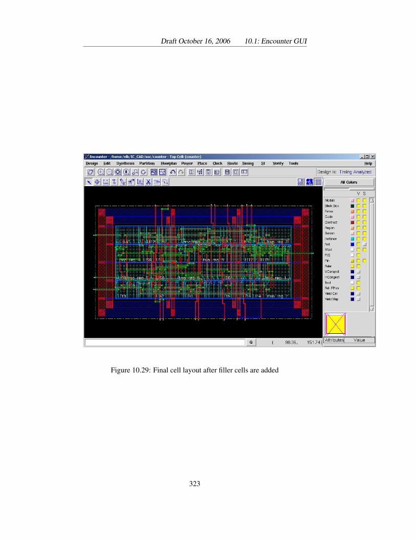
Draft October 16, 2006 10.1: Encounter GUI
Figure 10.29: Final cell layout after filler cells are added
323
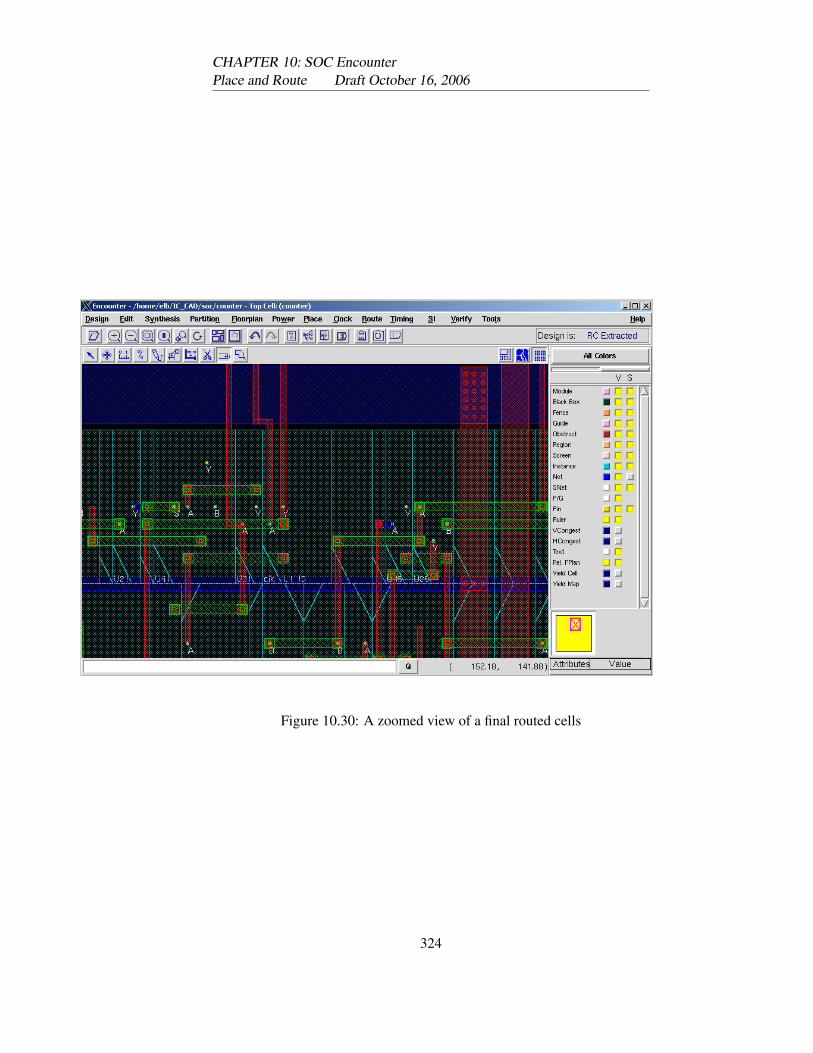
CHAPTER 10: SOC EncounterPlace and Route Draft October 16, 2006
Figure 10.30: A zoomed view of a final routed cells
324
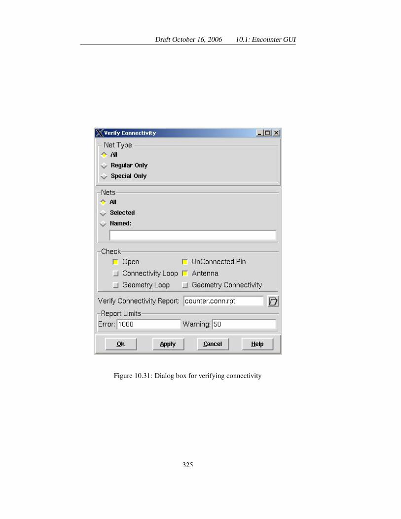
Draft October 16, 2006 10.1: Encounter GUI
Figure 10.31: Dialog box for verifying connectivity
325
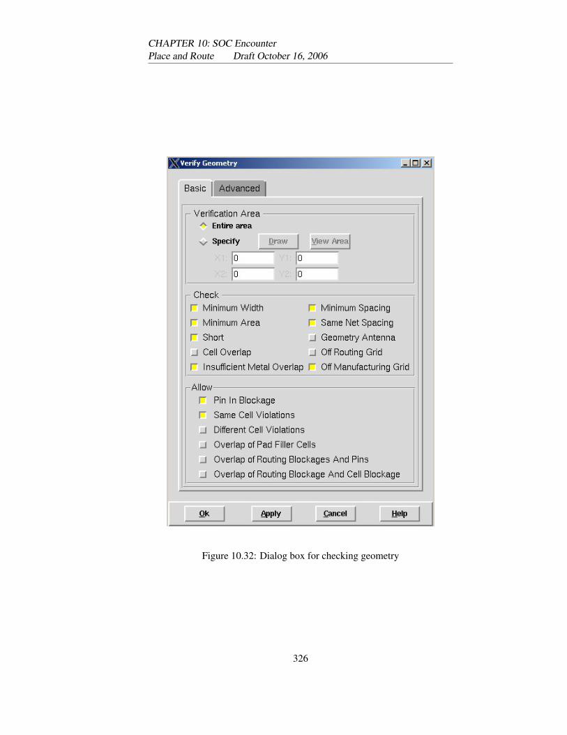
CHAPTER 10: SOC EncounterPlace and Route Draft October 16, 2006
Figure 10.32: Dialog box for checking geometry
326
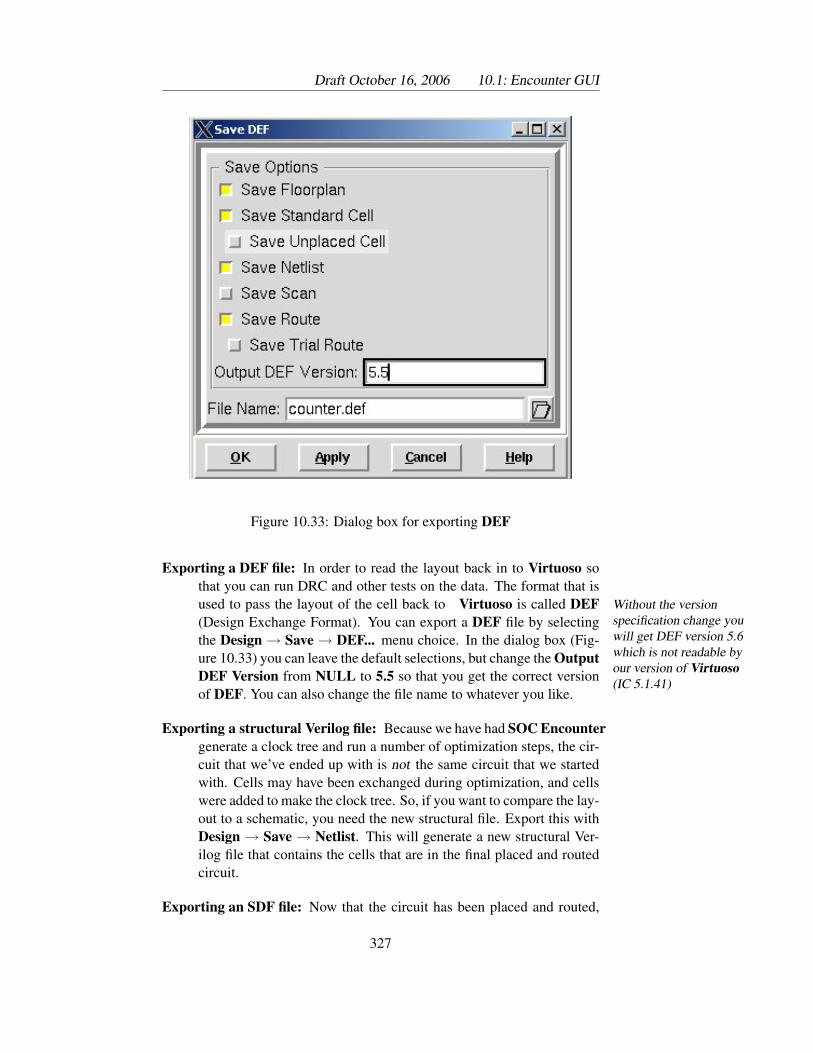
Draft October 16, 2006 10.1: Encounter GUI
Figure 10.33: Dialog box for exporting DEF
Exporting a DEF file: In order to read the layout back in to Virtuoso sothat you can run DRC and other tests on the data. The format that isused to pass the layout of the cell back to Virtuoso is called DEF Without the version
specification change youwill get DEF version 5.6which is not readable byour version of Virtuoso(IC 5.1.41)
(Design Exchange Format). You can export a DEF file by selectingthe Design → Save → DEF... menu choice. In the dialog box (Fig-ure 10.33) you can leave the default selections, but change the OutputDEF Version from NULL to 5.5 so that you get the correct versionof DEF. You can also change the file name to whatever you like.
Exporting a structural Verilog file: Because we have had SOC Encountergenerate a clock tree and run a number of optimization steps, the cir-cuit that we’ve ended up with is not the same circuit that we startedwith. Cells may have been exchanged during optimization, and cellswere added to make the clock tree. So, if you want to compare the lay-out to a schematic, you need the new structural file. Export this withDesign → Save → Netlist. This will generate a new structural Ver-ilog file that contains the cells that are in the final placed and routedcircuit.
Exporting an SDF file: Now that the circuit has been placed and routed,
327
CHAPTER 10: SOC EncounterPlace and Route Draft October 16, 2006
you can export an SDF (Standard Delay Format) file that has not onlytimings for the cells but timing extracted from the interconnect. Youcan use this file with your Verilog simulation if all your cells havebehavioral views with specify blocks for timing to get quite accu-rate timing in your behavioral simulation. Generate this file by firstselecting Timing → Extract RC to extract the RC timings of the in-terconnect. You can leave the default of just saving the capacitanceto the .cap file if you just want an SDF file, or you can select othertypes of RC output files. The SPEF file in particular can be used bythe Synopsys tool PrimeTime later for static timing analysis if youwant. Once you’ve extracted the RC information you can generate anSDF file with the Timing → Calculate Delay menu choice.
Exporting a LEF file: If you want to use this placed and routed cell as ablock in a larger circuit you need to export the cell as a LEF file andas a liberty file. That is, you could take this entire cell and instantiateit as a block in another larger circuit. It could be placed as a blockin the floorplanning stage and other standard cells could be placedand routed around the block. The LEF file would describe this entirecell as one MACRO, and you would include that LEF file in the listof LEF files in the design import phase. The .lib file would definethe timing of this cell. For some reason, exporting LEF and Libinformation is not in the menus. To generate these files you needto type the commands directly to the SOC Encounter prompt in theshell window. Type the commands:
do extract model -blackbox 2d -force counter.characterize.liblefOut counter.lef -stripePin -PGpinLayers 1 2
This will generate both .lib and .lef files that you can use later to in-clude this cell as a block in another circuit. The options to the lefOutcommand make sure that the power and ground rings and stripes areextracted in the cell macro. If you look at the .lef file you’ll notice thatthe cell macro is defined to be of CLASS BLOCK. This is differentfrom the lower level standard cells which are CLASS CORE. Thisindicates that this is a large block that should be placed separatelyfrom the standard cells in SOC Encounter.
10.1.12 Reading the Cell Back Into Virtuoso
Now your cell is complete so you can read it back in to Virtuoso for furtherprocessing (DRC, extract, and LVS) or for further use as a macro cell inother designs.
328
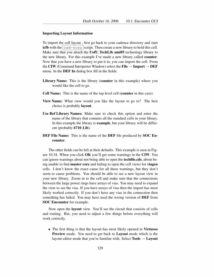
Draft October 16, 2006 10.1: Encounter GUI
Importing Layout Information
To import the cell layout , first go back to your cadence directory and starticfb with the cad-ncsu script. Then create a new library to hold this cell.Make sure that you attach the UofU TechLib ami05 technology library tothe new library. For this example I’ve made a new library called counter.Now that you have a new library to put it in, you can import the cell. Fromthe CIW (Command Interpreter Window) select the File→ Import→DEFmenu. In the DEF In dialog box fill in the fields:
Library Name: This is the library (counter in this example) where youwould like the cell to go.
Cell Name: This is the name of the top-level cell (counter in this case).
View Name: What view would you like the layout to go to? The bestchoice is probably layout.
Use Ref Library Names: Make sure to check this option and enter thename of the library that contains all the standard cells in your library.In this example the library is example, but your library will be differ-ent (probably 6710 Lib).
DEF File Name: This is the name of the DEF file produced by SOC En-counter.
The other fields can be left at their defaults. This example is seen in Fig-ure 10.34. When you click OK you’ll get some warnings in the CIW. Youcan ignore warnings about not being able to open the techfile.cds, about be-ing unable to find master core and failing to open the cell views for viagencells. I don’t know the exact cause for all these warnings, but they don’tseem to cause problems. You should be able to see a new layout view inyour new library. Zoom in to the cell and make sure that the connectionsbetween the large power rings have arrays of vias. You may need to expandthe view to see the vias. If you have arrays of vias then the import has mostlikely worked correctly. If you don’t have any vias in the connection thensomething has failed. You may have used the wrong version of DEF fromSOC Encounter for example.
Now open the layout view. You’ll see the circuit that consists of cellsand routing. But, you need to adjust a few things before everything willwork correctly.
• The first thing is that the layout has most likely opened in VirtuosoPreview mode. You need to get back to Layout mode which is thelayout editor mode that you’re familiar with. Select Tools → Layout
329
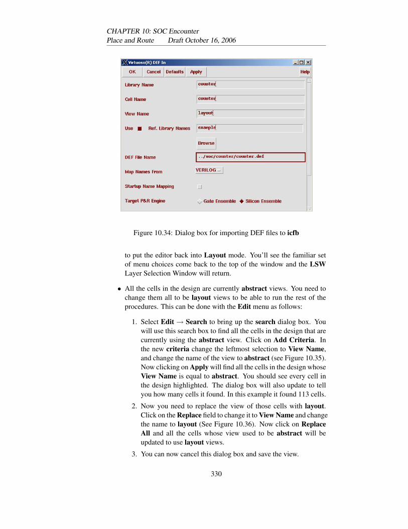
CHAPTER 10: SOC EncounterPlace and Route Draft October 16, 2006
Figure 10.34: Dialog box for importing DEF files to icfb
to put the editor back into Layout mode. You’ll see the familiar setof menu choices come back to the top of the window and the LSWLayer Selection Window will return.
• All the cells in the design are currently abstract views. You need tochange them all to be layout views to be able to run the rest of theprocedures. This can be done with the Edit menu as follows:
1. Select Edit → Search to bring up the search dialog box. Youwill use this search box to find all the cells in the design that arecurrently using the abstract view. Click on Add Criteria. Inthe new criteria change the leftmost selection to View Name,and change the name of the view to abstract (see Figure 10.35).Now clicking on Apply will find all the cells in the design whoseView Name is equal to abstract. You should see every cell inthe design highlighted. The dialog box will also update to tellyou how many cells it found. In this example it found 113 cells.
2. Now you need to replace the view of those cells with layout.Click on the Replace field to change it to View Name and changethe name to layout (See Figure 10.36). Now click on ReplaceAll and all the cells whose view used to be abstract will beupdated to use layout views.
3. You can now cancel this dialog box and save the view.
330
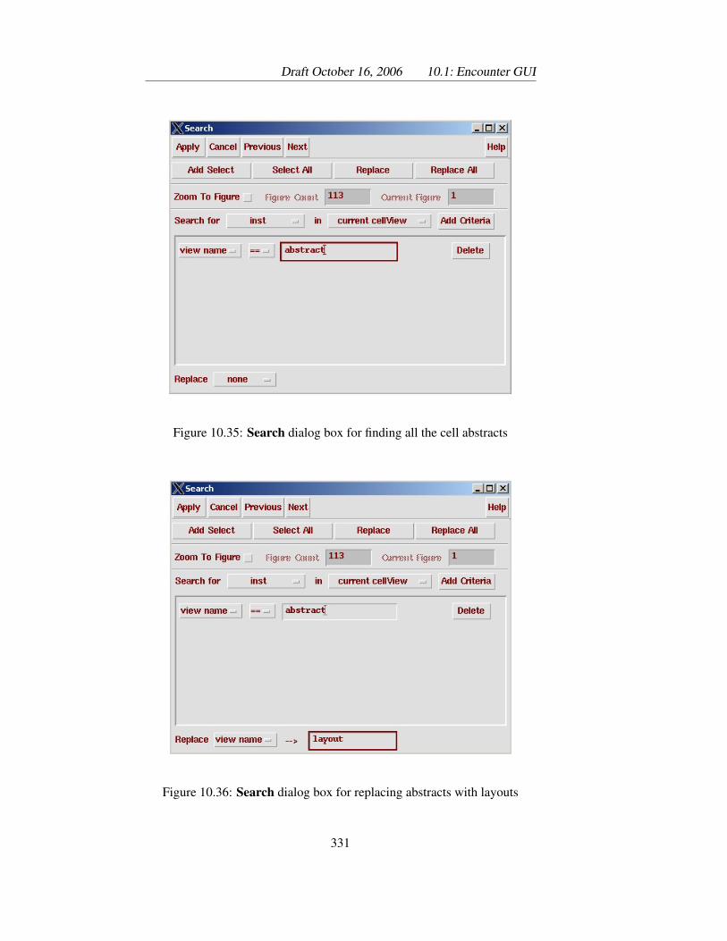
Draft October 16, 2006 10.1: Encounter GUI
Figure 10.35: Search dialog box for finding all the cell abstracts
Figure 10.36: Search dialog box for replacing abstracts with layouts
331
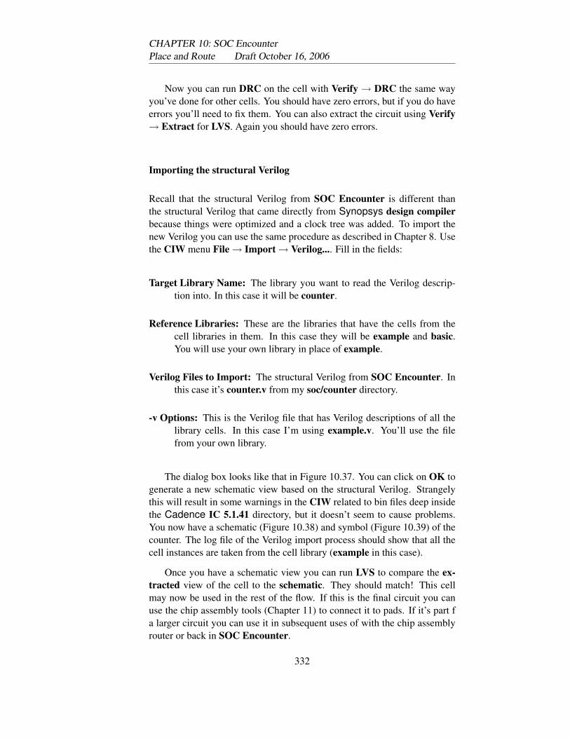
CHAPTER 10: SOC EncounterPlace and Route Draft October 16, 2006
Now you can run DRC on the cell with Verify → DRC the same wayyou’ve done for other cells. You should have zero errors, but if you do haveerrors you’ll need to fix them. You can also extract the circuit using Verify→ Extract for LVS. Again you should have zero errors.
Importing the structural Verilog
Recall that the structural Verilog from SOC Encounter is different thanthe structural Verilog that came directly from Synopsys design compilerbecause things were optimized and a clock tree was added. To import thenew Verilog you can use the same procedure as described in Chapter 8. Usethe CIW menu File → Import → Verilog.... Fill in the fields:
Target Library Name: The library you want to read the Verilog descrip-tion into. In this case it will be counter.
Reference Libraries: These are the libraries that have the cells from thecell libraries in them. In this case they will be example and basic.You will use your own library in place of example.
Verilog Files to Import: The structural Verilog from SOC Encounter. Inthis case it’s counter.v from my soc/counter directory.
-v Options: This is the Verilog file that has Verilog descriptions of all thelibrary cells. In this case I’m using example.v. You’ll use the filefrom your own library.
The dialog box looks like that in Figure 10.37. You can click on OK togenerate a new schematic view based on the structural Verilog. Strangelythis will result in some warnings in the CIW related to bin files deep insidethe Cadence IC 5.1.41 directory, but it doesn’t seem to cause problems.You now have a schematic (Figure 10.38) and symbol (Figure 10.39) of thecounter. The log file of the Verilog import process should show that all thecell instances are taken from the cell library (example in this case).
Once you have a schematic view you can run LVS to compare the ex-tracted view of the cell to the schematic. They should match! This cellmay now be used in the rest of the flow. If this is the final circuit you canuse the chip assembly tools (Chapter 11) to connect it to pads. If it’s part fa larger circuit you can use it in subsequent uses of with the chip assemblyrouter or back in SOC Encounter.
332
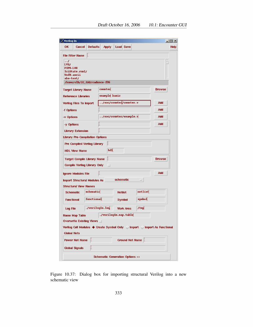
Draft October 16, 2006 10.1: Encounter GUI
Figure 10.37: Dialog box for importing structural Verilog into a newschematic view
333
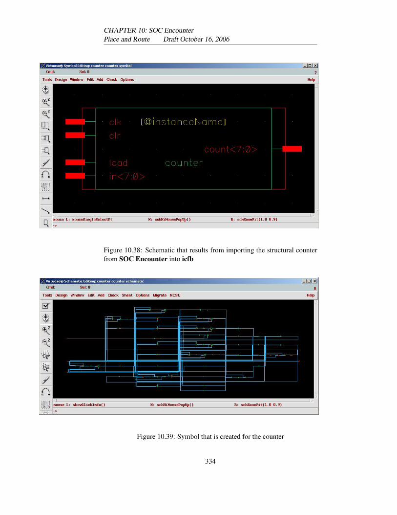
CHAPTER 10: SOC EncounterPlace and Route Draft October 16, 2006
Figure 10.38: Schematic that results from importing the structural counterfrom SOC Encounter into icfb
Figure 10.39: Symbol that is created for the counter
334
Draft October 16, 2006 10.2: Encounter Scripting
10.2 Encounter Scripting
SOC Encounter, like most CAD tools, can be driven either from the window-based GUI or from scripts. Once you’ve completed the process of place androute a few times from the GUI, you may want to automate parts of theprocess using scripts. In general, you probably want to do the floor plan-ning portion of the flow by hand, and then use a script for the rest of theflow (placement, optimization, clock tree synthesis, optimization, routing,optimization, exporting data).
You can always peruse the SOC Encounter Text Command ReferenceGuide in the documentation to see how to write the script commands, oryou can look in the output logs from your use of the GUI. SOC Encounterproduces two logs while you are using the GUI: encounter.log which logsthe messages in the shell window, and encounter.cmd which logs the com-mands that you execute while using the menus. You can use the encounter.cmdfile to replicate commands in scripts that you previously used in the GUI.
10.2.1 Design Import with Configuration Files
The first step in using SOC Encounter is to use the Design Import menu toread in your initial structural Verilog file. You can streamline this process byusing a configuration file. In the class directory related to SOC Encounter(/uusoc/facility/cad common/local/class/6710/cadence/SOC you will findan input configuration file called UofU soc.conf that you can customize foryour use. Change the file names and library names in the top portion ofthe file for your application before using it. The first part of this file, asconfigured for the counter example is shown in Figure 10.40. The fullconfiguration file template is shown in Appendix C, and, of course, you cansee it on-line.
To use this configuration file, after filling in your information, use theDesign → Design Import menu, but choose Load and then load the .conffile that you’ve customized for your circuit. This will read in the circuit withall the extra information in the other tabs already filled in.
10.2.2 Floor Planning
You can now proceed to the floor planning stage of the process using theFloorplan → Specify Floorplan menu. You’ll see that the Aspect Ratio,Core Utilization, and Core to IO Boundary fields will be already filled in,although may not be exactly 1, 0.7, and 30 (but they’ll be close!). You canmodify things, or accept the defaults. From this point you can proceed as
335
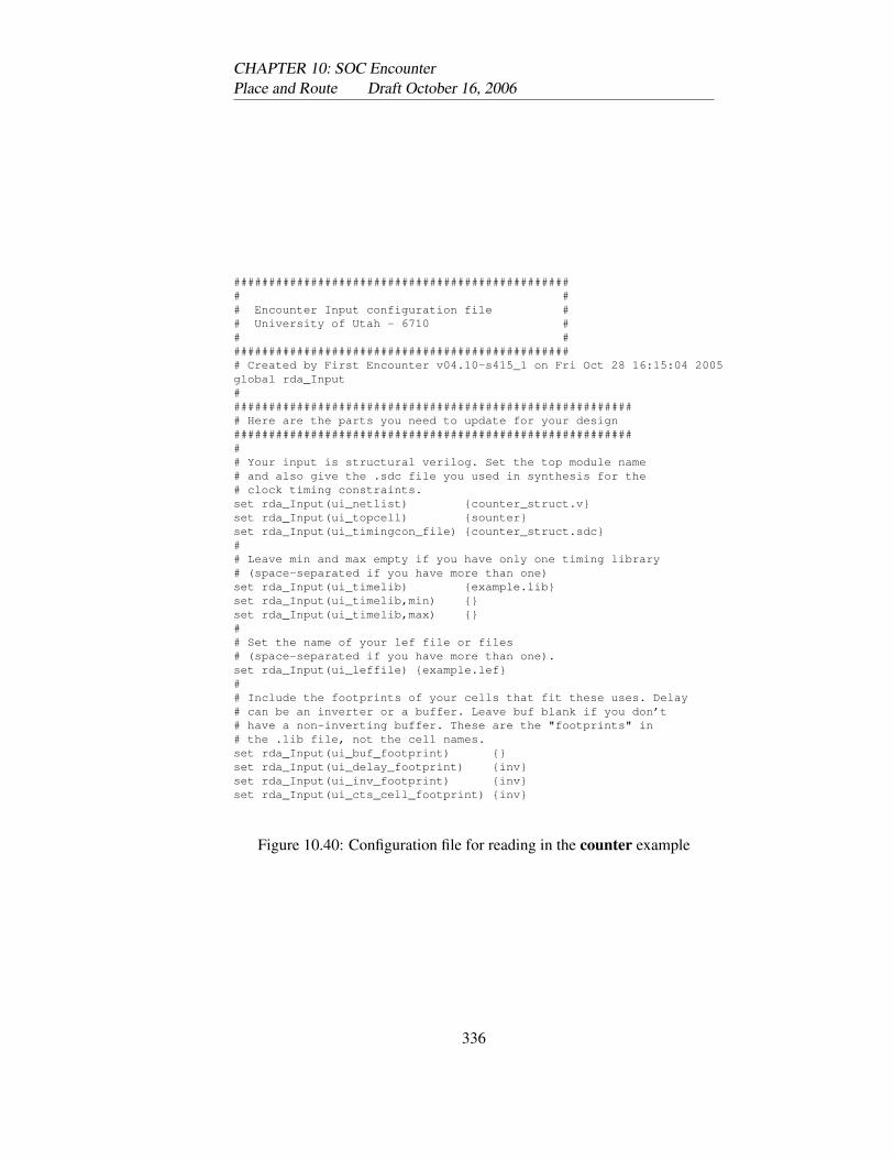
CHAPTER 10: SOC EncounterPlace and Route Draft October 16, 2006
################################################# ## Encounter Input configuration file ## University of Utah - 6710 ## ################################################## Created by First Encounter v04.10-s415_1 on Fri Oct 28 16:15:04 2005global rda_Input########################################################### Here are the parts you need to update for your design########################################################### Your input is structural verilog. Set the top module name# and also give the .sdc file you used in synthesis for the# clock timing constraints.set rda_Input(ui_netlist) {counter_struct.v}set rda_Input(ui_topcell) {sounter}set rda_Input(ui_timingcon_file) {counter_struct.sdc}## Leave min and max empty if you have only one timing library# (space-separated if you have more than one)set rda_Input(ui_timelib) {example.lib}set rda_Input(ui_timelib,min) {}set rda_Input(ui_timelib,max) {}## Set the name of your lef file or files# (space-separated if you have more than one).set rda_Input(ui_leffile) {example.lef}## Include the footprints of your cells that fit these uses. Delay# can be an inverter or a buffer. Leave buf blank if you don’t# have a non-inverting buffer. These are the "footprints" in# the .lib file, not the cell names.set rda_Input(ui_buf_footprint) {}set rda_Input(ui_delay_footprint) {inv}set rda_Input(ui_inv_footprint) {inv}set rda_Input(ui_cts_cell_footprint) {inv}
Figure 10.40: Configuration file for reading in the counter example
336
Draft October 16, 2006 10.2: Encounter Scripting
in the previous sections. The <filename>.conf configuration file will havemade the Design Import process much easier.
10.2.3 Complete Scripting
You could run through the rest of the flow by hand at this point, or you couldscript the rest of the flow. In the class directory you’ll find a complete scriptthat runs through the entire flow. This script is called UofU opt.tcl. Youcan modify this script for your own use. You may, for example, want to runthrough the floor planning by hand, and run the script for everything else. Oryou may want to adjust your configuration file for the floorplan you want,and run the script for everything. Or you might want to extract portions ofthe script to run separately. You can also use the script as a starting pointand add new commands based on the commands that you’ve run in the GUI.It’s all up to you! This script is not meant to be the end-all be-all of scripts.It’s just a starting point.
I haven’t yet found a way to execute scripts from the GUI or the shellonce SOC Encounter is running. Instead, you can run the script fromthe initial program execution with cad-soc -init <scriptfile>which will run the script when the program starts up. The first part ofthe UofU opt.tcl script is shown in Figure 10.41 as I configured it for thecounter example. The full script is in the class directory and in Appendix C.Remember that if you try something that works well in the GUI, you canlook in the encounter.cmd log file to find the text version of that commandto add to your own script.
337
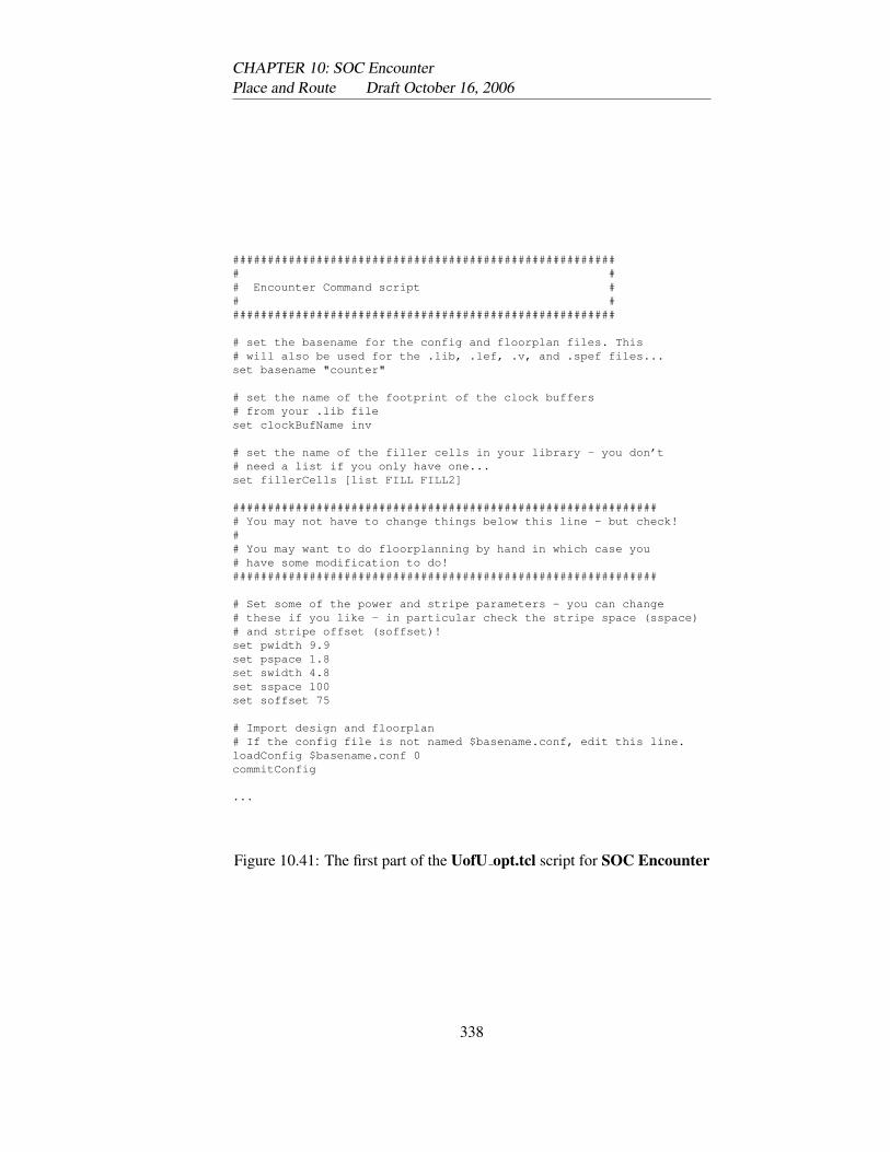
CHAPTER 10: SOC EncounterPlace and Route Draft October 16, 2006
######################################################## ## Encounter Command script ## ########################################################
# set the basename for the config and floorplan files. This# will also be used for the .lib, .lef, .v, and .spef files...set basename "counter"
# set the name of the footprint of the clock buffers# from your .lib fileset clockBufName inv
# set the name of the filler cells in your library - you don’t# need a list if you only have one...set fillerCells [list FILL FILL2]
############################################################## You may not have to change things below this line - but check!## You may want to do floorplanning by hand in which case you# have some modification to do!#############################################################
# Set some of the power and stripe parameters - you can change# these if you like - in particular check the stripe space (sspace)# and stripe offset (soffset)!set pwidth 9.9set pspace 1.8set swidth 4.8set sspace 100set soffset 75
# Import design and floorplan# If the config file is not named $basename.conf, edit this line.loadConfig $basename.conf 0commitConfig
...
Figure 10.41: The first part of the UofU opt.tcl script for SOC Encounter
338
Chapter 11
Chip Assembly
THE PROCESS of wiring up pre-designed modules to make a completechip core, or taking a finished core and routing it to the chip padsis known as chip assembly. Cadence has yet another tool that is
designed specifically for this set of tasks known as the Cadence Chip As-sembly Router (ccar) which is part of the IC Craftsman (ICC) tool set.This tool will route between large pre-designed blocks which are not placedon a regular grid. This makes it fundamentally different than SOC En-counter which wants to place small cells on a fixed grid. The blocks thatare routed by ccar could be blocks that are placed and routed by SOC En-counter, or could also be blocks that are designed by hand or by other tools(i.e. custom datapath circuits, memories, or other dense regular arrays). Al-though there are certainly more features of ccar then are described here, weuse ccar strictly for routing. That is, the user places the blocks by hand,connects the global power and ground nets, then uses ccar to connect thesignal wires between those large blocks. The ccar tool is also used to routebetween finished cores and the pad ring.
11.1 Module Routing with ccar
The ccar tool, unlike other tools we’ve used so far, is not invoked directly.Instead it is used in conjunction with the Cadence Composer and Virtuosotools. The overall process is:
1. Make a schematic that contains your modules connected together. In-put and output pins should be used to indicate signals that enter andleave the collection of modules.
2. Use Virtuoso-XL to generate a new layout based on that schematic.

CHAPTER 11: Chip Assembly Draft October 30, 2006
3. Place the modules by hand in the layout view.
4. Place the IO pins that were defined in the schematic (and generated inthe layout) in the desired spots in the layout.
5. Connect vdd! and gnd! so that the modules are connected to a com-mon power network.
6. Export the layout view to ccar for signal routing
7. Route the signal nets in ccar
8. Import the routed module back to Virtuoso-XL. Then DRC, extract,and LVS.
So, to start out you need:
1. The modules that you will be connecting need to have layout viewsthat have all the connection points marked with shape pins of the righttype (metal1, metal2, or metal3) and named the same things as on thesymbol (blocks routed by SOC Encounter already have these).
2. For each cell you also need a symbol view of that cell that has thesame pins on the interface of the symbol that are in the layout (cellblocks imported from the structural Verilog view generated by SOCEncounter have these symbols too).
3. You need a schematic showing the connection of parts that you wantto route together. That is, you make a schematic that includes in-stances of the parts that you want to use, and all the connections be-tween them. This is a good thing to have in general because you’llneed it to simulate the functionality of the schematic and for LVSanyway. It’s also what tells ccar which signals it should route and towhere.
4. A rules file for the IC Craftsman (icc) ccar router called icc.rul.Copy this file from/uusoc/facility/cad common/local/class/6710/cadence/ICC to the di-rectory from which you start cad-ncsu.
5. Also copy the do.do file from that same class directory to the directoryfrom which you start cad-ncsu. You’ll need both of these later whenyou start up ccar.
What this process will do is generate a connected layout that corre-sponds to the schematic. You will do the placement by hand, but the router
340
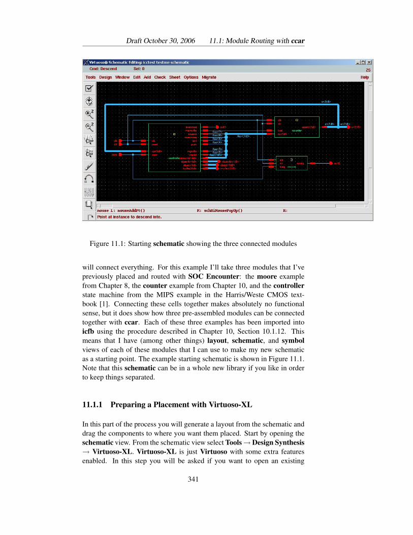
Draft October 30, 2006 11.1: Module Routing with ccar
Figure 11.1: Starting schematic showing the three connected modules
will connect everything. For this example I’ll take three modules that I’vepreviously placed and routed with SOC Encounter: the moore examplefrom Chapter 8, the counter example from Chapter 10, and the controllerstate machine from the MIPS example in the Harris/Weste CMOS text-book [1]. Connecting these cells together makes absolutely no functionalsense, but it does show how three pre-assembled modules can be connectedtogether with ccar. Each of these three examples has been imported intoicfb using the procedure described in Chapter 10, Section 10.1.12. Thismeans that I have (among other things) layout, schematic, and symbolviews of each of these modules that I can use to make my new schematicas a starting point. The example starting schematic is shown in Figure 11.1.Note that this schematic can be in a whole new library if you like in orderto keep things separated.
11.1.1 Preparing a Placement with Virtuoso-XL
In this part of the process you will generate a layout from the schematic anddrag the components to where you want them placed. Start by opening theschematic view. From the schematic view select Tools→Design Synthesis→ Virtuoso-XL. Virtuoso-XL is just Virtuoso with some extra featuresenabled. In this step you will be asked if you want to open an existing
341
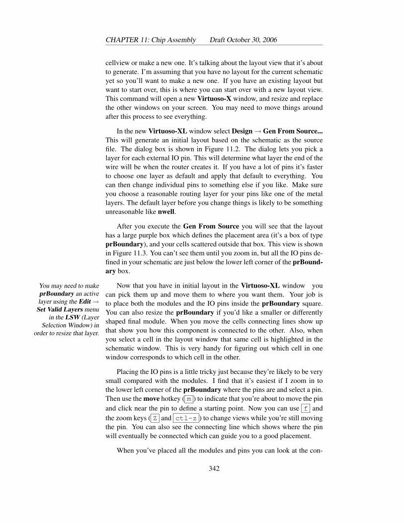
CHAPTER 11: Chip Assembly Draft October 30, 2006
cellview or make a new one. It’s talking about the layout view that it’s aboutto generate. I’m assuming that you have no layout for the current schematicyet so you’ll want to make a new one. If you have an existing layout butwant to start over, this is where you can start over with a new layout view.This command will open a new Virtuoso-X window, and resize and replacethe other windows on your screen. You may need to move things aroundafter this process to see everything.
In the new Virtuoso-XL window select Design→Gen From Source...This will generate an initial layout based on the schematic as the sourcefile. The dialog box is shown in Figure 11.2. The dialog lets you pick alayer for each external IO pin. This will determine what layer the end of thewire will be when the router creates it. If you have a lot of pins it’s fasterto choose one layer as default and apply that default to everything. Youcan then change individual pins to something else if you like. Make sureyou choose a reasonable routing layer for your pins like one of the metallayers. The default layer before you change things is likely to be somethingunreasonable like nwell.
After you execute the Gen From Source you will see that the layouthas a large purple box which defines the placement area (it’s a box of typeprBoundary), and your cells scattered outside that box. This view is shownin Figure 11.3. You can’t see them until you zoom in, but all the IO pins de-fined in your schematic are just below the lower left corner of the prBound-ary box.
Now that you have in initial layout in the Virtuoso-XL window youYou may need to makeprBoundary an activelayer using the Edit →
Set Valid Layers menuin the LSW (Layer
Selection Window) inorder to resize that layer.
can pick them up and move them to where you want them. Your job isto place both the modules and the IO pins inside the prBoundary square.You can also resize the prBoundary if you’d like a smaller or differentlyshaped final module. When you move the cells connecting lines show upthat show you how this component is connected to the other. Also, whenyou select a cell in the layout window that same cell is highlighted in theschematic window. This is very handy for figuring out which cell in onewindow corresponds to which cell in the other.
Placing the IO pins is a little tricky just because they’re likely to be verysmall compared with the modules. I find that it’s easiest if I zoom in tothe lower left corner of the prBoundary where the pins are and select a pin.Then use the move hotkey ( m ) to indicate that you’re about to move the pinand click near the pin to define a starting point. Now you can use f andthe zoom keys ( Z and ctl-z ) to change views while you’re still movingthe pin. You can also see the connecting line which shows where the pinwill eventually be connected which can guide you to a good placement.
When you’ve placed all the modules and pins you can look at the con-
342
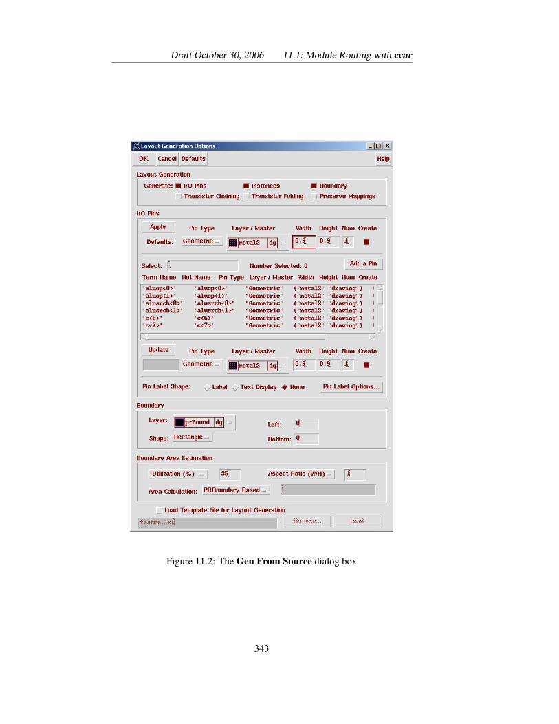
Draft October 30, 2006 11.1: Module Routing with ccar
Figure 11.2: The Gen From Source dialog box
343
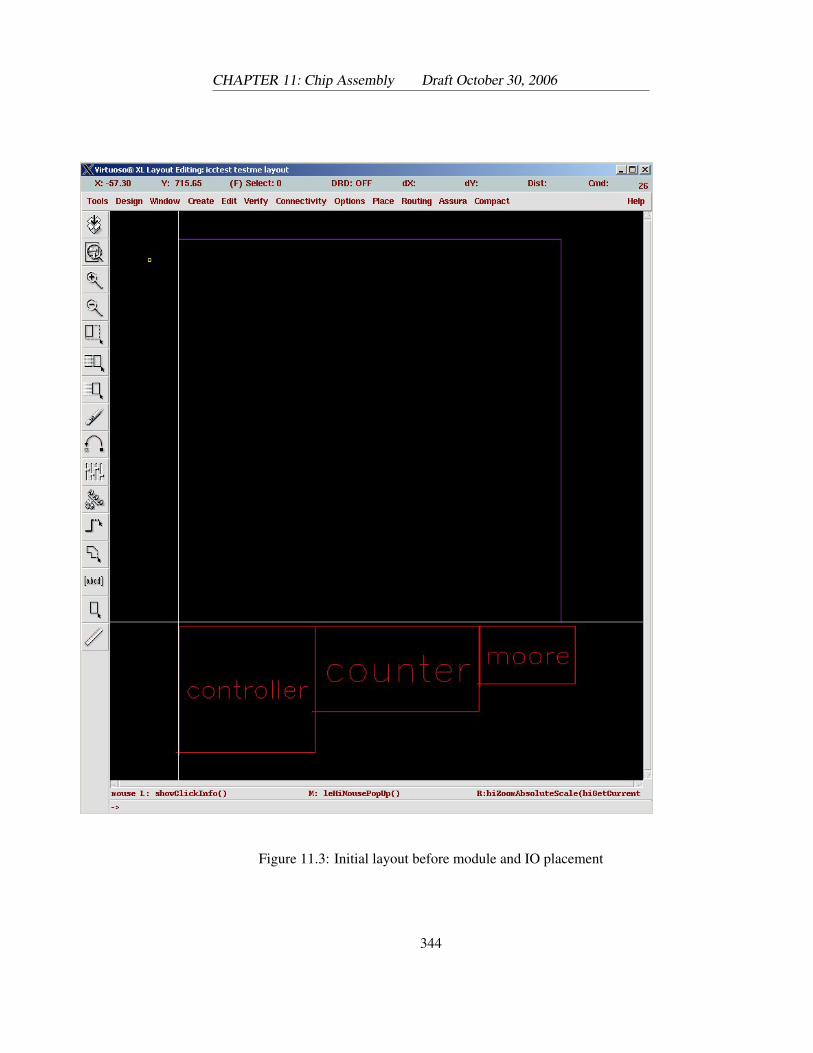
CHAPTER 11: Chip Assembly Draft October 30, 2006
Figure 11.3: Initial layout before module and IO placement
344
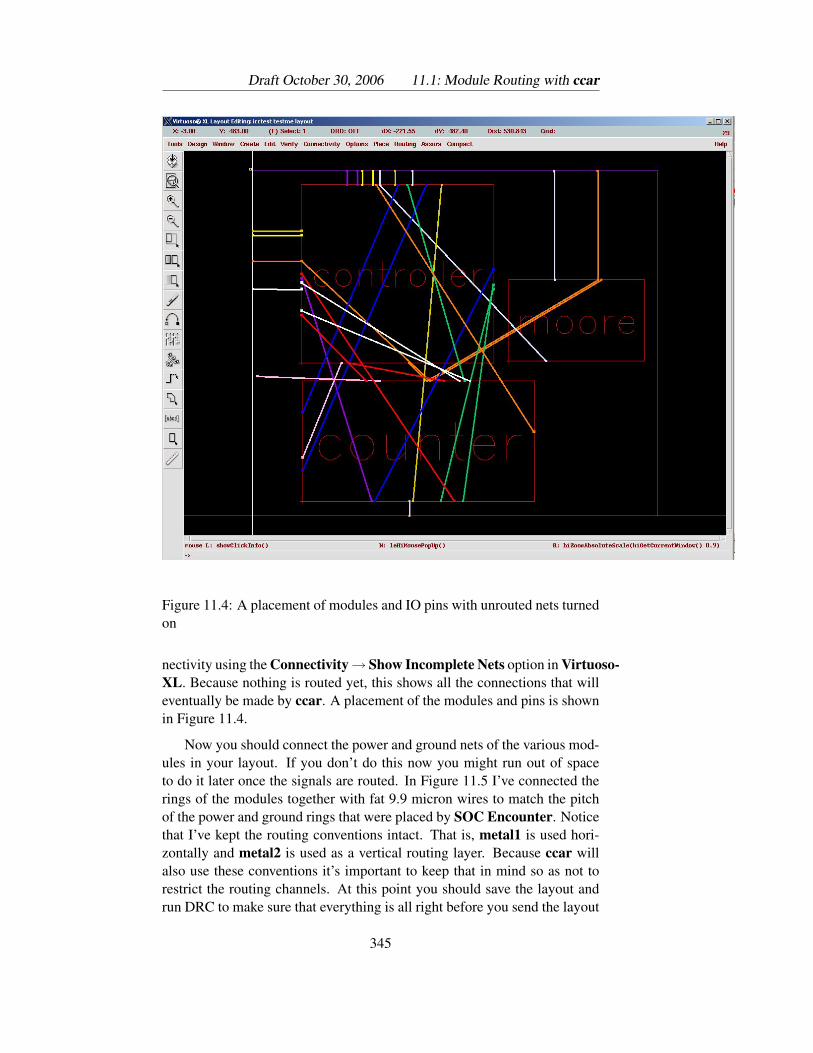
Draft October 30, 2006 11.1: Module Routing with ccar
Figure 11.4: A placement of modules and IO pins with unrouted nets turnedon
nectivity using the Connectivity→ Show Incomplete Nets option in Virtuoso-XL. Because nothing is routed yet, this shows all the connections that willeventually be made by ccar. A placement of the modules and pins is shownin Figure 11.4.
Now you should connect the power and ground nets of the various mod-ules in your layout. If you don’t do this now you might run out of spaceto do it later once the signals are routed. In Figure 11.5 I’ve connected therings of the modules together with fat 9.9 micron wires to match the pitchof the power and ground rings that were placed by SOC Encounter. Noticethat I’ve kept the routing conventions intact. That is, metal1 is used hori-zontally and metal2 is used as a vertical routing layer. Because ccar willalso use these conventions it’s important to keep that in mind so as not torestrict the routing channels. At this point you should save the layout andrun DRC to make sure that everything is all right before you send the layout
345
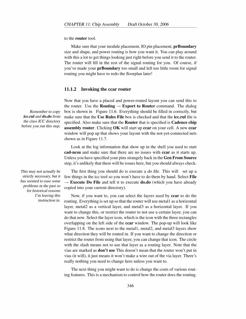
CHAPTER 11: Chip Assembly Draft October 30, 2006
to the router tool.
Make sure that your module placement, IO pin placement, prBoundarysize and shape, and power routing is how you want it. You can play aroundwith this a lot to get things looking just right before you send it to the router.The router will fill in the rest of the signal routing for you. Of course, ifyou’ve made your prBoundary too small and left too little room for signalrouting you might have to redo the floorplan later!
11.1.2 Invoking the ccar router
Now that you have a placed and power-routed layout you can send this tothe router. Use the Routing → Export to Router command. The dialogbox is shown in Figure 11.6. Everything should be filled in correctly, butRemember to copy
icc.rul and do.do fromthe class ICC directory
before you run this step.
make sure that the Use Rules File box is checked and that the icc.rul file isspecified. Also make sure that the Router that is specified is Cadence chipassembly router. Clicking OK will start up ccar on your cell. A new ccarwindow will pop up that shows your layout with the not-yet-connected netsshown as in Figure 11.7.
Look at the log information that show up in the shell you used to startcad-ncsu and make sure that there are no issues with ccar as it starts up.Unless you have specified your pins strangely back in the Gen From Sourcestep, it’s unlikely that there will be issues here, but you should always check.
The first thing you should do is execute a do file. This will set up aThis may not actually bestrictly necessary, but it
has seemed to ease someproblems in the past so
for historical reasonsI’m leaving this
instruction in.
few things in the icc tool so you won’t have to do them by hand. Select File→ Execute Do File and tell it to execute do.do (which you have alreadycopied into your current directory).
Now, if you want to, you can select the layers used by ccar to do therouting. Everything is set up so that the router will use metal1 as a horizontallayer, metal2 as a vertical layer, and metal3 as a horizontal layer. If youwant to change this, or restrict the router to not use a certain layer, you cando that now. Select the layer icon, which is the icon with the three rectanglesoverlapping on the left side of the ccar window. The pop-up will look likeFigure 11.8. The icons next to the metal1, metal2, and metal3 layers showwhat direction they will be routed in. If you want to change the direction orrestrict the router from using that layer, you can change that icon. The circlewith the slash means not to use that layer as a routing layer. Note that thevias are marked as don’t use This doesn’t mean that the router won’t put invias (it will), it just means it won’t make a wire out of the via layer. There’sreally nothing you need to change here unless you want to.
The next thing you might want to do is change the costs of various rout-ing features. This is a mechanism to control how the router does the routing.
346
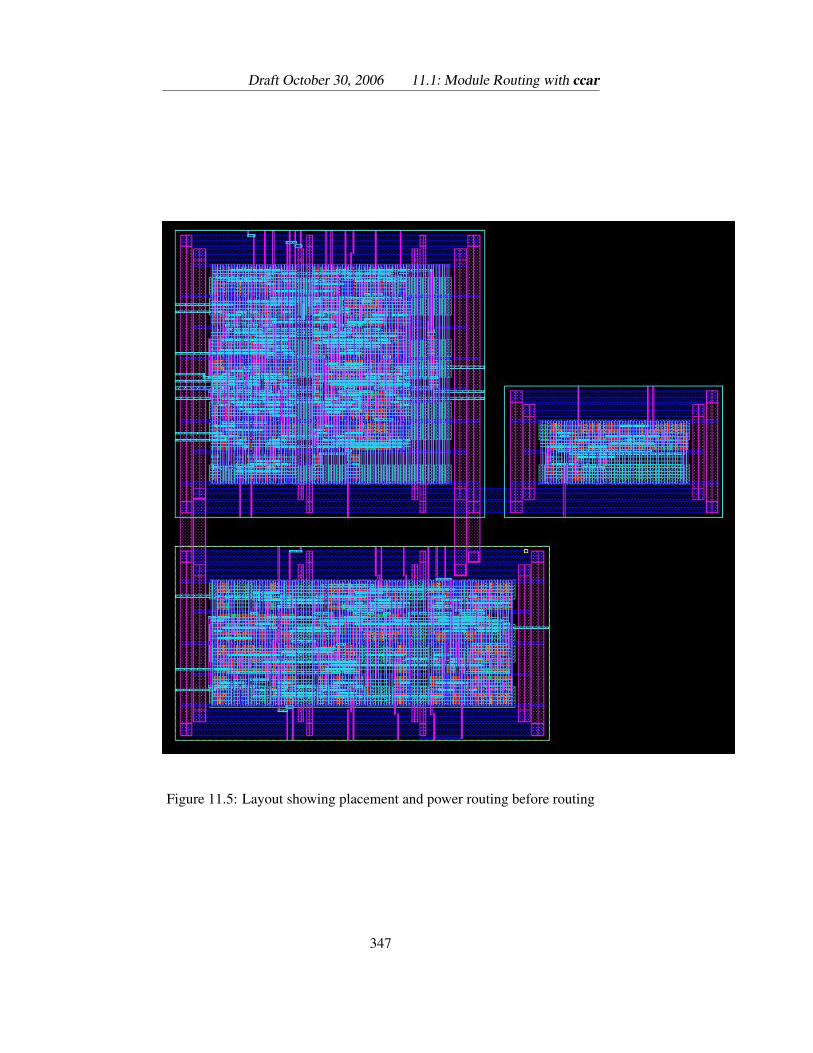
Draft October 30, 2006 11.1: Module Routing with ccar
Figure 11.5: Layout showing placement and power routing before routing
347
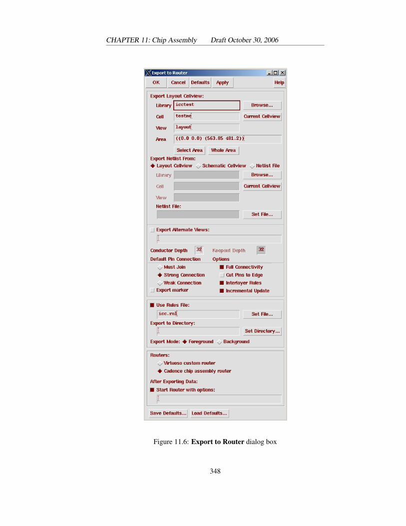
CHAPTER 11: Chip Assembly Draft October 30, 2006
Figure 11.6: Export to Router dialog box
348
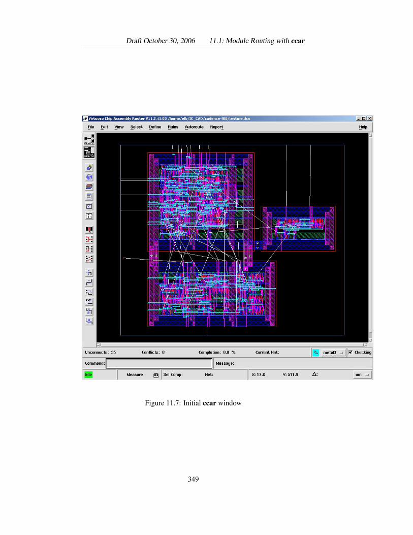
Draft October 30, 2006 11.1: Module Routing with ccar
Figure 11.7: Initial ccar window
349
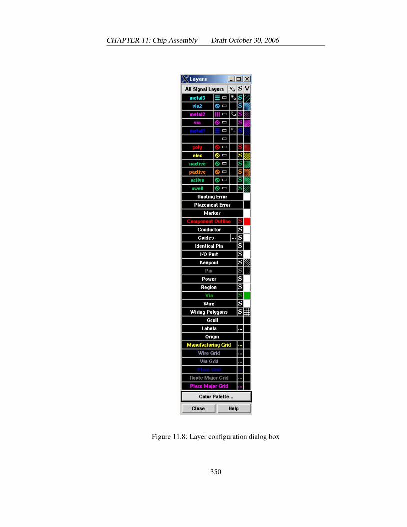
CHAPTER 11: Chip Assembly Draft October 30, 2006
Figure 11.8: Layer configuration dialog box
350
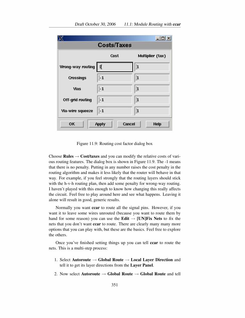
Draft October 30, 2006 11.1: Module Routing with ccar
Figure 11.9: Routing cost factor dialog box
Choose Rules → Cost/taxes and you can modify the relative costs of vari-ous routing features. The dialog box is shown in Figure 11.9. The -1 meansthat there is no penalty. Putting in any number raises the cost penalty in therouting algorithm and makes it less likely that the router will behave in thatway. For example, if you feel strongly that the routing layers should stickwith the h-v-h routing plan, then add some penalty for wrong-way routing.I haven’t played with this enough to know how changing this really affectsthe circuit. Feel free to play around here and see what happens. Leaving italone will result in good, generic results.
Normally you want ccar to route all the signal pins. However, if youwant it to leave some wires unrouted (because you want to route them byhand for some reason) you can use the Edit → [UN]Fix Nets to fix thenets that you don’t want ccar to route. There are clearly many many moreoptions that you can play with, but these are the basics. Feel free to explorethe others.
Once you’ve finished setting things up you can tell ccar to route thenets. This is a multi-step process:
1. Select Autoroute → Global Route → Local Layer Direction andtell it to get its layer directions from the Layer Panel.
2. Now select Autoroute → Global Route → Global Route and tell
351
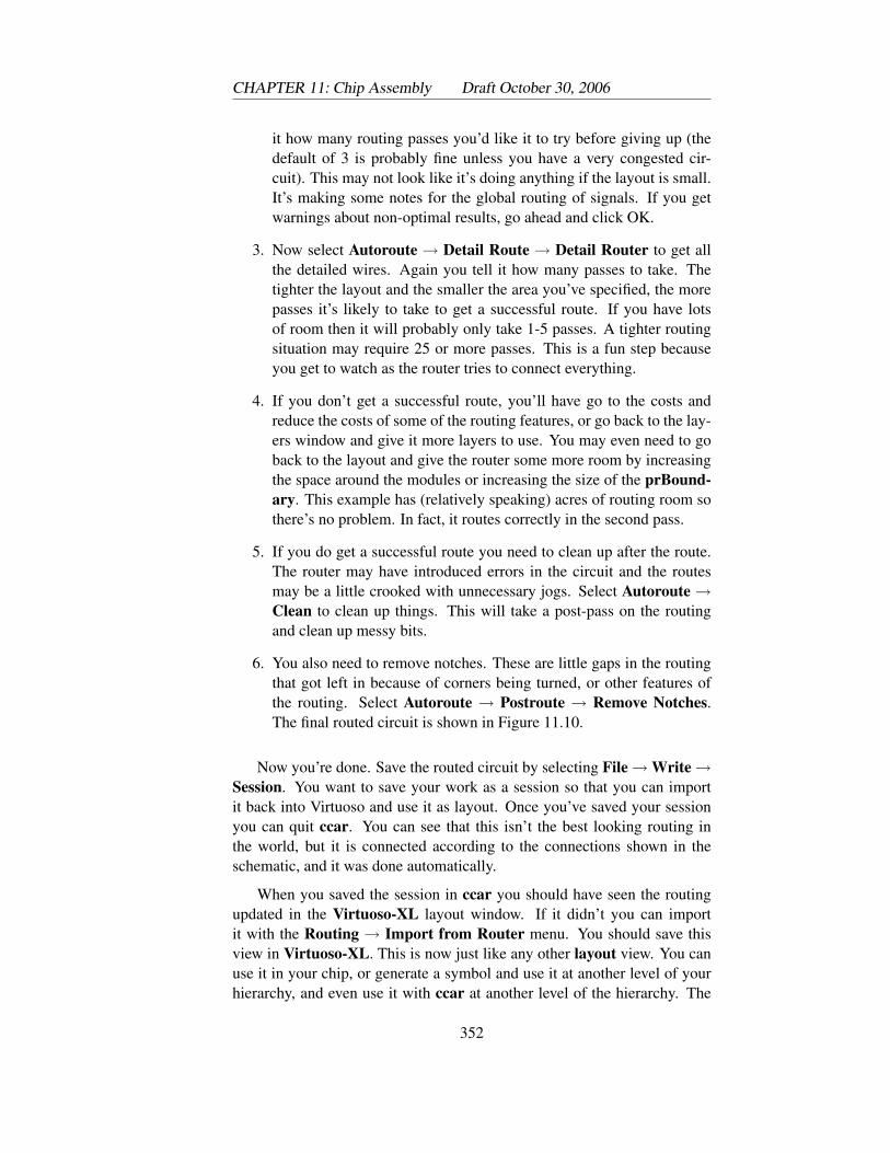
CHAPTER 11: Chip Assembly Draft October 30, 2006
it how many routing passes you’d like it to try before giving up (thedefault of 3 is probably fine unless you have a very congested cir-cuit). This may not look like it’s doing anything if the layout is small.It’s making some notes for the global routing of signals. If you getwarnings about non-optimal results, go ahead and click OK.
3. Now select Autoroute → Detail Route → Detail Router to get allthe detailed wires. Again you tell it how many passes to take. Thetighter the layout and the smaller the area you’ve specified, the morepasses it’s likely to take to get a successful route. If you have lotsof room then it will probably only take 1-5 passes. A tighter routingsituation may require 25 or more passes. This is a fun step becauseyou get to watch as the router tries to connect everything.
4. If you don’t get a successful route, you’ll have go to the costs andreduce the costs of some of the routing features, or go back to the lay-ers window and give it more layers to use. You may even need to goback to the layout and give the router some more room by increasingthe space around the modules or increasing the size of the prBound-ary. This example has (relatively speaking) acres of routing room sothere’s no problem. In fact, it routes correctly in the second pass.
5. If you do get a successful route you need to clean up after the route.The router may have introduced errors in the circuit and the routesmay be a little crooked with unnecessary jogs. Select Autoroute →Clean to clean up things. This will take a post-pass on the routingand clean up messy bits.
6. You also need to remove notches. These are little gaps in the routingthat got left in because of corners being turned, or other features ofthe routing. Select Autoroute → Postroute → Remove Notches.The final routed circuit is shown in Figure 11.10.
Now you’re done. Save the routed circuit by selecting File → Write →Session. You want to save your work as a session so that you can importit back into Virtuoso and use it as layout. Once you’ve saved your sessionyou can quit ccar. You can see that this isn’t the best looking routing inthe world, but it is connected according to the connections shown in theschematic, and it was done automatically.
When you saved the session in ccar you should have seen the routingupdated in the Virtuoso-XL layout window. If it didn’t you can importit with the Routing → Import from Router menu. You should save thisview in Virtuoso-XL. This is now just like any other layout view. You canuse it in your chip, or generate a symbol and use it at another level of yourhierarchy, and even use it with ccar at another level of the hierarchy. The
352
Draft October 30, 2006 11.1: Module Routing with ccar
Figure 11.10: Final routed circuit (shown in Virtuoso window)
353
CHAPTER 11: Chip Assembly Draft October 30, 2006
only difference between this and a layout view that you did by hand is thatafter you did a placement of the cells by hand in this example, the ChipAssembly Router did the interconnect for you.
Once you have the layout back in Virtuoso, you will want to do the usualthings to it: DRC and LVS for example. The first thing you should do is runDRC to make sure that the autorouted circuit does not have any new DRCerrors in it. Although the autorouter is good, it’s not perfect and it may leavea few small errors around. In particular, you may get metal spacing errorsat the point where the autorouted wires connect to the SOC-routed block.This is because the connections that SOC uses are shape pins that use pintype material instead of drawing type material. You can see this if you openthe SOC-routed layout and zoom in close to one of the IO pins. The IOSOC uses pin layers for
the IO pins that itgenerates, and an
extracted view uses netpurpose layers for the
extracted nets.
pin that SOC put in looks different than real metal. Each of the layers inCadence is really a layer-purpose pair. That is, there is a set of layers, anda set of purposes, and each layer can be paired with a purpose. Normallyyou’re using drawing purpose. The layers in your LSW have a little dgafter them to show that they’re drawing-purpose layers.
If you do have metal spacing errors, you can fix them by hand by puttinga small piece of metal over the mistake, or you can fix them by editing yourSOC layout. To do this, open the SOC layout. Then use the Edit→ Searchdialog to find all rectangles on layer metal1 pn (or metal2 pn or metal3 pndepending on where you put your pins), and change them to layer their dgversions. This will convert them to drawing purpose layers and the DRCprocess should stop complaining.
If you have any other DRC errors, you need to check them out and fixthem.
Now you can LVS against the schematic that you used to define theconnectivity in the first place. This is done in the usual way generate anextracted view, LVS the extracted against the schematic. The only thingyou need to be careful of here is to make sure vdd! and gnd! were connectedbefore you try to LVS. You will need to connect these supply nets by hand(which you should have done before you routed the module).
11.2 Core to Pad Frame Routing with ccar
In this section I will walk through the procedure for using icc to connectActually, it does matterfor a grade in the class.
Everyone shouldconnect their core to thepads for the final report
even if the core isn’tworking completely yet!
your chip core to a pad frame. Before you start the process of connectingyour core, you need a complete core! A complete core is the complete gutsof your chip with all the components connected, all the vdd! and gnd! linesconnected, and simulated for functionality. If you don’t have a functional,simulated, complete core, then it doesn’t matter whether it has pads around
354
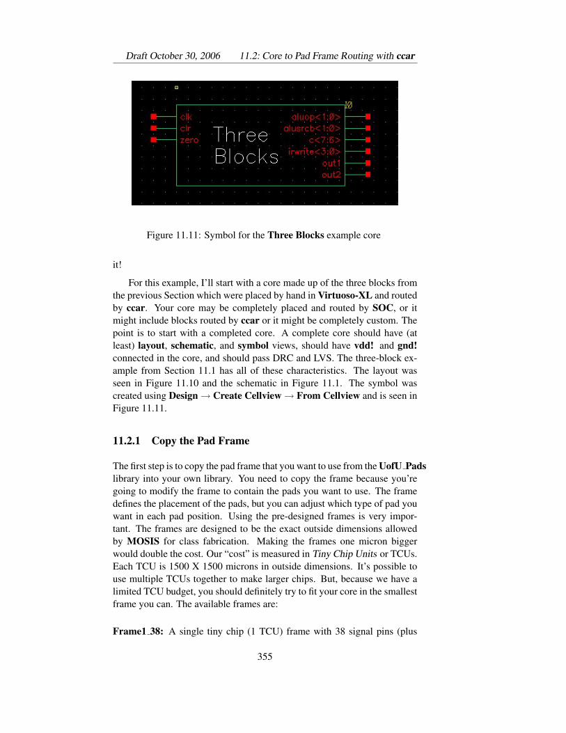
Draft October 30, 2006 11.2: Core to Pad Frame Routing with ccar
Figure 11.11: Symbol for the Three Blocks example core
it!
For this example, I’ll start with a core made up of the three blocks fromthe previous Section which were placed by hand in Virtuoso-XL and routedby ccar. Your core may be completely placed and routed by SOC, or itmight include blocks routed by ccar or it might be completely custom. Thepoint is to start with a completed core. A complete core should have (atleast) layout, schematic, and symbol views, should have vdd! and gnd!connected in the core, and should pass DRC and LVS. The three-block ex-ample from Section 11.1 has all of these characteristics. The layout wasseen in Figure 11.10 and the schematic in Figure 11.1. The symbol wascreated using Design → Create Cellview → From Cellview and is seen inFigure 11.11.
11.2.1 Copy the Pad Frame
The first step is to copy the pad frame that you want to use from the UofU Padslibrary into your own library. You need to copy the frame because you’regoing to modify the frame to contain the pads you want to use. The framedefines the placement of the pads, but you can adjust which type of pad youwant in each pad position. Using the pre-designed frames is very impor-tant. The frames are designed to be the exact outside dimensions allowedby MOSIS for class fabrication. Making the frames one micron biggerwould double the cost. Our “cost” is measured in Tiny Chip Units or TCUs.Each TCU is 1500 X 1500 microns in outside dimensions. It’s possible touse multiple TCUs together to make larger chips. But, because we have alimited TCU budget, you should definitely try to fit your core in the smallestframe you can. The available frames are:
Frame1 38: A single tiny chip (1 TCU) frame with 38 signal pins (plus
355
CHAPTER 11: Chip Assembly Draft October 30, 2006
1-vdd and 1-gnd). Usable core area is approximately 900 X 900 mi-crons.
Frame2h 70: A two-tiny-chip (2 TCU) frame with 70 signal pins (plus 1-vdd and 1-gnd). The core a horizontal rectangle (long edges on topand bottom). Usable core area is approximately 2300 X 900 microns.If you aren’t using all the signal pad locations and want to add extrapower and ground pads you can add them as follows: vdd on pads 16and 33, gnd on pads 48 and 74.
Frame2v 70: A two-tiny-chip (2 TCU) frame with 70 signal pins (plus 1-vdd and 1-gnd). The core a vertical rectangle (long edges on right andleft). Usable core area is approximately 900 X 2300 microns. If youaren’t using all the signal pad locations and want to add extra powerand ground pads you can add them as follows: vdd on pads 16 and33, gnd on pads 48 and 74.
Frame4 78: A four-tiny-chip frame with 78 signal pins (plus 3-vdd and3-gnd). Usable core area is approximately 2300 X 2300 microns.
For this example I’ll use the Frame1 38. I’ll copy that cell from theUofU Pads library to my own library so that I can modify for the needs ofthe core.
11.2.2 Modify the Frame schematic view
Once the frame of your choice is copied into the library you are using forchip assembly, you need to replace pads that are in the frame with the padsyou want. The frames have vdd and gnd pads in the correct places for thetester so DO NOT change the location of the vdd and gnd pads! All theother pads in the frame are pad nc for no-connect. You should replace thepad nc cells with the pads you want. The cells available are:
pad bidirhe: A bidirectional (tri-state) pad with high-enable. From thecore to the pad the signals are DataOut and EN. These are outputsfrom your core, and inputs to the pad cell. From the pad to the corethe signals are DataIn and DataInB. These are outputs from the padand inputs to your core. The pad itself is connected to an inout pincalled pad.
pad in: An input pad meaning from the outside world to your core. Thesignals are DataIn and DataInB going from the pad to your core.The pad itself is on an input pin called pad.
356
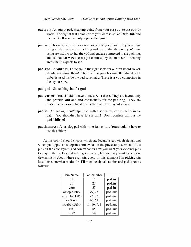
Draft October 30, 2006 11.2: Core to Pad Frame Routing with ccar
pad out: An output pad, meaning going from your core out to the outsideworld. The signal that comes from your core is called DataOut, andthe pad itself is on an output pin called pad.
pad nc: This is a pad that does not connect to your core. If you are notusing all the pads in the pad ring make sure that the ones you’re notusing are pad nc so that the vdd and gnd are connected in the pad ring,and so that MOSIS doesn’t get confused by the number of bondingareas that it expects to see.
pad vdd: A vdd pad. These are in the right spots for our test board so youshould not move them! There are no pins because the global vdd!Label is used inside the pad schematic. There is a vdd connection inthe layout view.
pad gnd: Same thing, but for gnd.
pad corner: You shouldn’t have to mess with these. They are layout-onlyand provide vdd and gnd connectivity for the pad ring. They areplaced in the correct locations in the pad frame layout views.
pad io: An analog input/output pad with a series resistor in the io signalpath. You shouldn’t have to use this! Don’t confuse this for thepad bidirhe!
pad io nores: An analog pad with no series resistor. You shouldn’t have touse this either!
At this point I should choose which pad locations get which signals andwhich pad type. This depends somewhat on the physical placement of thepins on the core layout, and somewhat on how you want your external pinsto map to the package. Anything will work, but you may want to be moredeterministic about where each pin goes. In this example I’m picking pinlocations somewhat randomly. I’ll map the signals to pins and pad types asfollows:
Pin Name Pad Numberclk 15 pad inclr 27 pad in
zero 37 pad inaluop<1:0> 79, 78 pad out
alusrcb<1:0> 73, 72 pad outc<7:6> 70, 69 pad out
irwrite<3:0> 11, 10, 9, 8 pad outout1 55 pad outout2 54 pad out
357
CHAPTER 11: Chip Assembly Draft October 30, 2006
This involves changing the appropriate pad nc cells into pad in andpad out cells in the schematic view. You can use the q Object PropertiesIt’s possible that the
origins of the cells maybe in different spots and
you may have to movethings around to keep
things looking neat.
menu to change which cell is instantiated in that spot without moving thecell.
Once I’ve made the cell type changes, I will add wires and pins to the ap-propriate cell inputs and outputs. What we’re aiming for is to define the in-put and output signals of the frame, collect this into a symbol view, and thenmake another schematic that has our core and frame connected together.This will be the starting point for the ccar router to route the signal pins tothe pads.
Now add input, output, and inout (if you have bidirectional pads) pins(and wires) to your frame schematic. There are two types of pins that youneed to add: signals coming from the outside world to your pad ring (theseconnect to the pad pins on the pad cells as if you were wiring the externalsignals to the pads), and signals going between your pad ring and your core(connecting to the DataIn, DataInB, and DataOut pins on the pad cells).The pad frame for this example is shown in Figure 11.12.
Make sure to get the directions right! Remember that going from yourcore to the pad frame is an output as far as the overall chip is concerned, butthat will be an input to the frame cell because it’s coming in to the framefrom your core. Likewise, a signal going from your pad frame to the coreis an input to your core because it’s coming into your core from the outsideworld, but it’s an output with respect to your frame cell. Think of the frameas a doughnut with the core in the hole. Outputs from your core go into theinside edge of the doughnut and emerge at the pads on the outside edge ofthe doughnut.
I like to name the pins that go between the core and the pad frame to bethe names of the signals with a i suffix for “internal,” and use the existing“real” signal names on the signals that are on the pads. That way I can keeptrack of which signals are internal and which are on the pads and connectto the outside world. It also lets me use the same testbench on the versionwith pads as with just the core itself. Of course you can come up with yourown naming scheme. An example of my naming scheme is seen in Fig-I modified the frame
symbol slightly toposition the pins of the
symbol in a “nice” waywith respect to the core
symbol.
ure 11.13. An automatically generated frame symbol is seen in Figure 11.14where it is connected to the core macro in a core-with-pads schematic viewthat I’ll call wholechip. The frame symbol was generated automatically us-ing the Design→ Create Cellview→ From Cellview menu. Note that I’vecollected some of the buses into bus pins in the frame schematic, and leftsome expanded as individual wires just to show that both are possible.
When I save the wholechip schematic I get some warnings about theDataInB signals being floating outputs. I didn’t connect them because Iwasn’t using them, so I’ll ignore those warnings. Unconnected outputs are
358
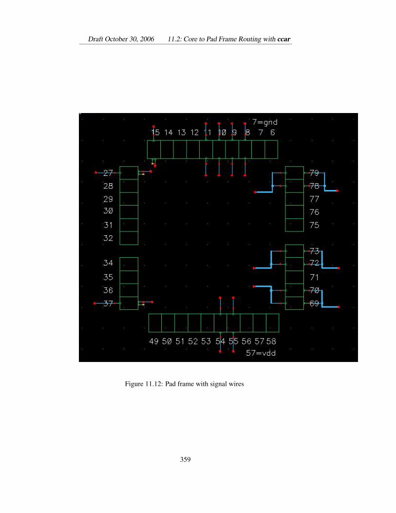
Draft October 30, 2006 11.2: Core to Pad Frame Routing with ccar
Figure 11.12: Pad frame with signal wires
359
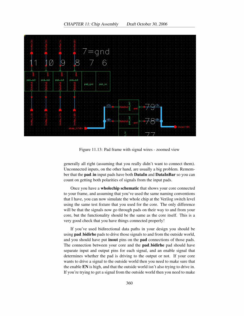
CHAPTER 11: Chip Assembly Draft October 30, 2006
Figure 11.13: Pad frame with signal wires - zoomed view
generally all right (assuming that you really didn’t want to connect them).Unconnected inputs, on the other hand, are usually a big problem. Remem-ber that the pad in input pads have both DataIn and DataInBar so you cancount on getting both polarities of signals from the input pads.
Once you have a wholechip schematic that shows your core connectedto your frame, and assuming that you’ve used the same naming conventionsthat I have, you can now simulate the whole chip at the Verilog switch levelusing the same test fixture that you used for the core. The only differencewill be that the signals now go through pads on their way to and from yourcore, but the functionality should be the same as the core itself. This is avery good check that you have things connected properly!
If you’ve used bidirectional data paths in your design you should beusing pad bidirhe pads to drive those signals to and from the outside world,and you should have put inout pins on the pad connections of those pads.The connection between your core and the pad bidirhe pad should haveseparate input and output pins for each signal, and an enable signal thatdetermines whether the pad is driving to the output or not. If your corewants to drive a signal to the outside world then you need to make sure thatthe enable EN is high, and that the outside world isn’t also trying to drive in.If you’re trying to get a signal from the outside world then you need to make
360
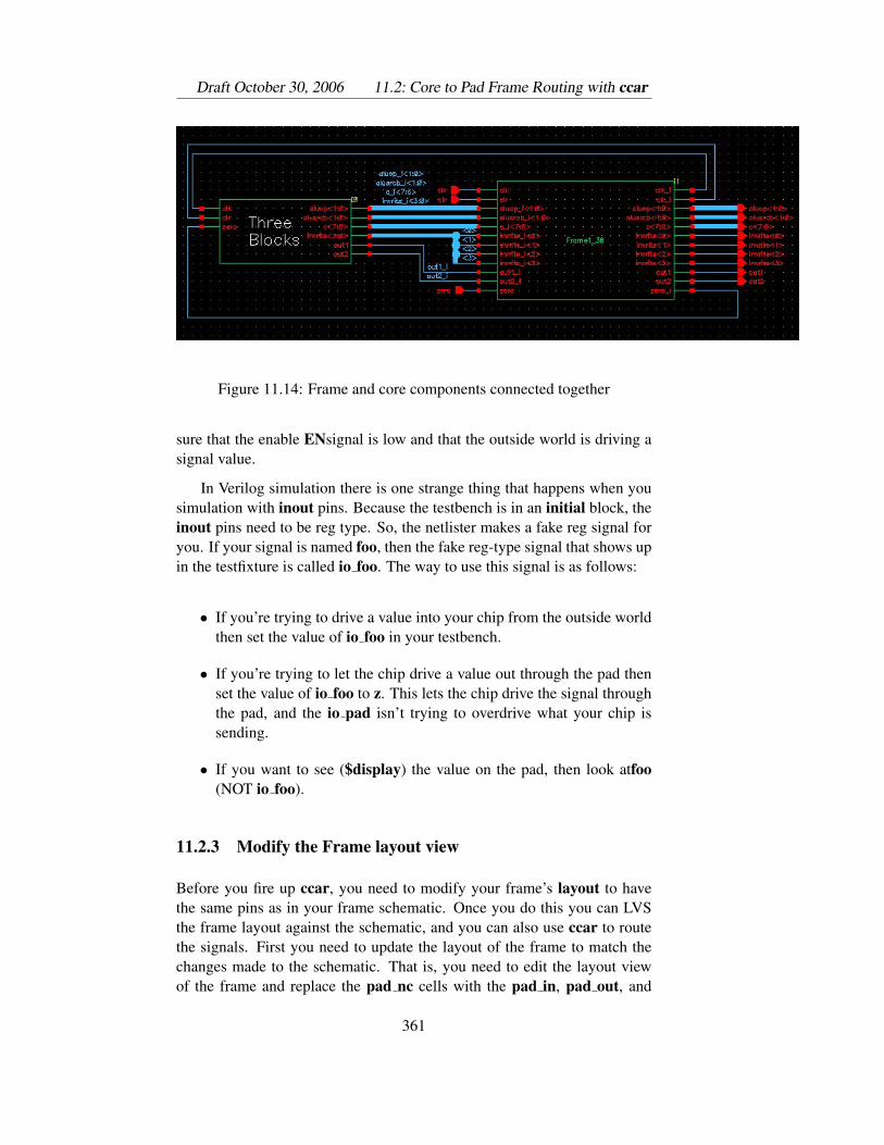
Draft October 30, 2006 11.2: Core to Pad Frame Routing with ccar
Figure 11.14: Frame and core components connected together
sure that the enable ENsignal is low and that the outside world is driving asignal value.
In Verilog simulation there is one strange thing that happens when yousimulation with inout pins. Because the testbench is in an initial block, theinout pins need to be reg type. So, the netlister makes a fake reg signal foryou. If your signal is named foo, then the fake reg-type signal that shows upin the testfixture is called io foo. The way to use this signal is as follows:
• If you’re trying to drive a value into your chip from the outside worldthen set the value of io foo in your testbench.
• If you’re trying to let the chip drive a value out through the pad thenset the value of io foo to z. This lets the chip drive the signal throughthe pad, and the io pad isn’t trying to overdrive what your chip issending.
• If you want to see ($display) the value on the pad, then look atfoo(NOT io foo).
11.2.3 Modify the Frame layout view
Before you fire up ccar, you need to modify your frame’s layout to havethe same pins as in your frame schematic. Once you do this you can LVSthe frame layout against the schematic, and you can also use ccar to routethe signals. First you need to update the layout of the frame to match thechanges made to the schematic. That is, you need to edit the layout viewof the frame and replace the pad nc cells with the pad in, pad out, and
361
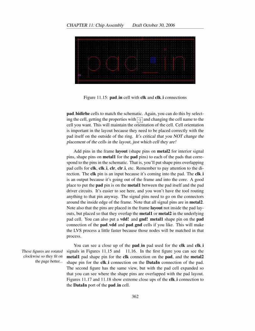
CHAPTER 11: Chip Assembly Draft October 30, 2006
Figure 11.15: pad in cell with clk and clk i connections
pad bidirhe cells to match the schematic. Again, you can do this by select-ing the cell, getting the properties with q and changing the cell name to thecell you want. This will maintain the orientation of the cell. Cell orientationis important in the layout because they need to be placed correctly with thepad itself on the outside of the ring. It’s critical that you NOT change theplacement of the cells in the layout, just which cell they are!
Add pins in the frame layout (shape pins on metal2 for interior signalpins, shape pins on metal1 for the pad pins) to each of the pads that corre-spond to the pins in the schematic. That is, you’ll put shape pins overlappingpad cells for clk, clk i, clr, clr i, etc. Remember to pay attention to the di-rection. The clk pin is an input because it’s coming into the pad. The clk iis an output because it’s going out of the frame and into the core. A goodplace to put the pad pin is on the metal1 between the pad itself and the paddriver circuits. It’s easier to see here, and you won’t have the tool routinganything to that pin anyway. The signal pins need to go on the connectorsaround the inside edge of the frame. Note that all signal pins are in metal2.Note also that the pins are placed in the frame layout not inside the pad lay-outs, but placed so that they overlap the metal1 or metal2 in the underlyingpad cell. You can also put a vdd! and gnd! metal1 shape pin on the padconnection of the pad vdd and pad gnd cells if you like. This will makethe LVS process a little faster because those nodes will be matched in thatprocess.
You can see a close up of the pad in pad used for the clk and clk isignals in Figures 11.15 and 11.16. In the first figure you can see theThese figures are rotated
clockwise so they fit onthe page better...
metal1 pad shape pin for the clk connection on the pad, and the metal2shape pin for the clk i connection on the DataIn connection of the pad.The second figure has the same view, but with the pad cell expanded sothat you can see where the shape pins are overlapped with the pad layout.Figures 11.17 and 11.18 show extreme close ups of the clk i connection tothe DataIn port of the pad in cell.
362
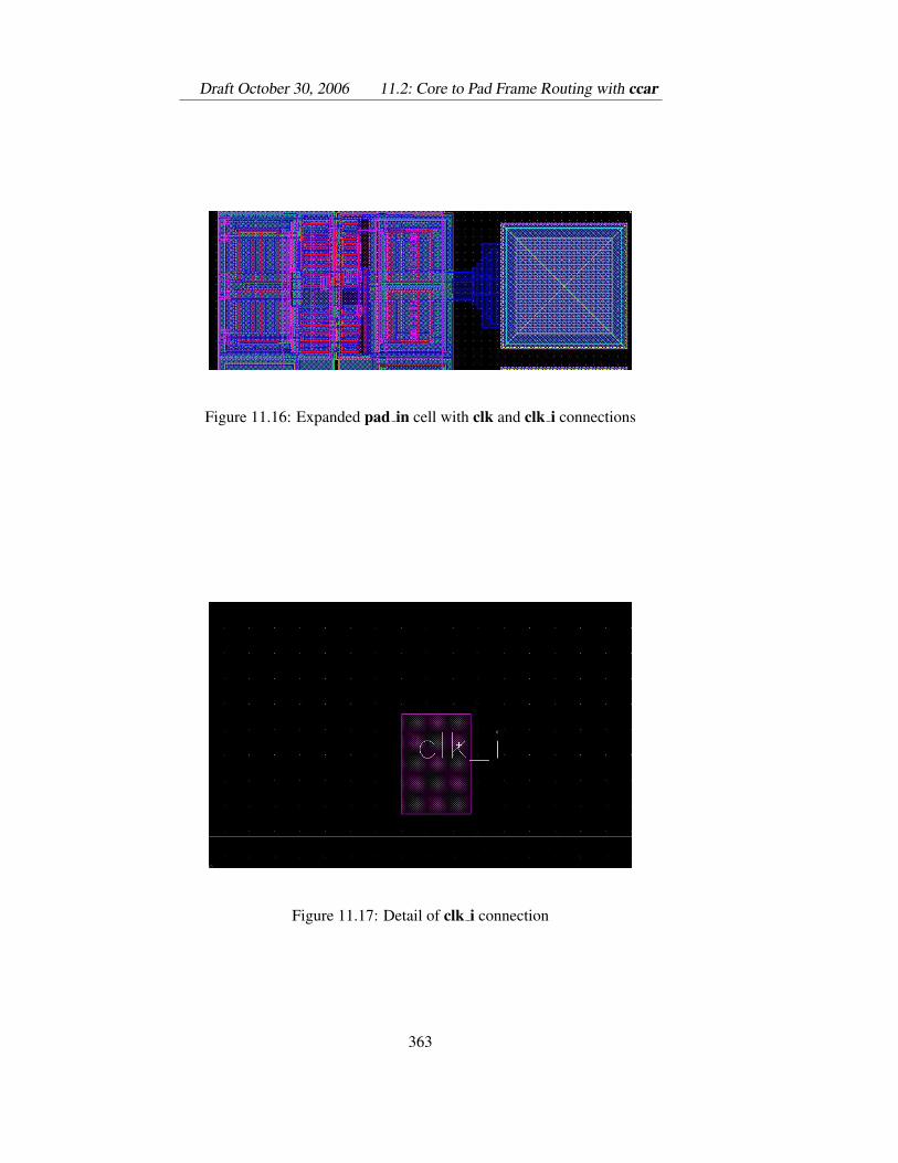
Draft October 30, 2006 11.2: Core to Pad Frame Routing with ccar
Figure 11.16: Expanded pad in cell with clk and clk i connections
Figure 11.17: Detail of clk i connection
363
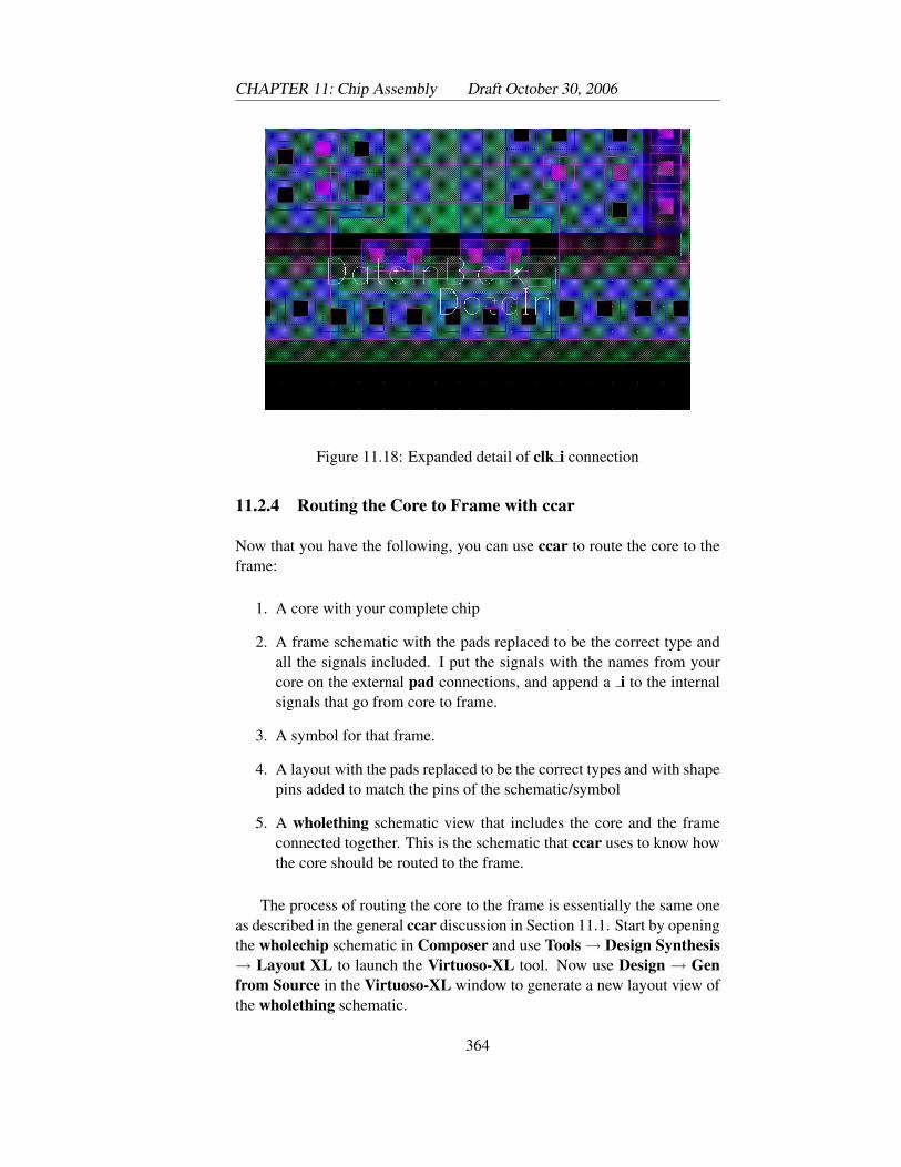
CHAPTER 11: Chip Assembly Draft October 30, 2006
Figure 11.18: Expanded detail of clk i connection
11.2.4 Routing the Core to Frame with ccar
Now that you have the following, you can use ccar to route the core to theframe:
1. A core with your complete chip
2. A frame schematic with the pads replaced to be the correct type andall the signals included. I put the signals with the names from yourcore on the external pad connections, and append a i to the internalsignals that go from core to frame.
3. A symbol for that frame.
4. A layout with the pads replaced to be the correct types and with shapepins added to match the pins of the schematic/symbol
5. A wholething schematic view that includes the core and the frameconnected together. This is the schematic that ccar uses to know howthe core should be routed to the frame.
The process of routing the core to the frame is essentially the same oneas described in the general ccar discussion in Section 11.1. Start by openingthe wholechip schematic in Composer and use Tools → Design Synthesis→ Layout XL to launch the Virtuoso-XL tool. Now use Design → Genfrom Source in the Virtuoso-XL window to generate a new layout view ofthe wholething schematic.
364
Draft October 30, 2006 11.2: Core to Pad Frame Routing with ccar
In the Gen from Source dialog box you have a chance to select whichpins you want to create. Pins are created for signals that are routed from thislayout view to an external pin so that the resulting routed layout can be usedhierarchically. In this case, the external connections are all to pads. In otherwords, there are no pins that you want created because there are no pins thatare exported outside this cell. All the connections are made internal to thewholechip schematic. All the connections are made to connect the core tothe frame. In the Gen from Source dialog box select all the pins (whichshould be only external pads, not the internal i signals) and turn off thecreate box. In the dialog box select all pins, turn off the create button, andpress Update. Also un-select the Generate I/O Pins button in the LayoutGeneration section. This way none of those pins will be created.
Now you can place the frame and core layouts in Virtuoso-XL. Grabthe frame and put it inside the purple prBoundary. You’ll probably want toexpand the view so that you can see inside the cells. Now move the core tobe inside the pad frame. When you do the placement in Virtuoso-XL youshould see the lines that connect the core to the frame. See Figure 11.19 foran example. You can see that I didn’t do a particularly good job of placingthe pad frame pins in convenient locations for the core. For this examplethat’s fine because there’s lots of routing room. For your chip you mightwant to think about this a little more carefully.
Check to make sure that there aren’t any stray pads (like vdd! and gnd!)down in the lower left just below the prBoundary. If there are, delete them!You don’t want icc to route anything but the signal pads. If you didn’tmanage to get all the signal pins turned off in the Gen from-Source step,here’s another chance to get rid of them.
Before you send this to the router, you need to connect vdd! and gnd!.Look at the pad vdd and pad gnd pads. There are big metal1 connectionpoints for vdd and gnd in the middle of the edge of the pad cell. The powertabs should be 28.8u wide. These are what you use to make a connectionbetween vdd and gnd from the pads to your core. Use the largest wires thatmake sense, and remember to put arrays of contacts if you have to switchlayers to connect large wires. DRC is a good idea at this point before yousend things to the router! there’s a view of the core placed inside the padframe just before I send it to the ccar router in Figure 11.20.
Now that I have a placed and power-routed core and frame layout, Ican send it to the ccar router with the Routing → Export to Router com-mand as in Section 11.1. The initial view in the ccar router is shown inFigure 11.21. You can now perform the routing (set the costs/taxes, set lo-cal layer direction, global route, detail route, cleanup, and remove notches).The result (seen after importing back into Virtuoso is seen in Figure 11.22.This layout should then be processed for DRC, Extract, and LVS to make
365
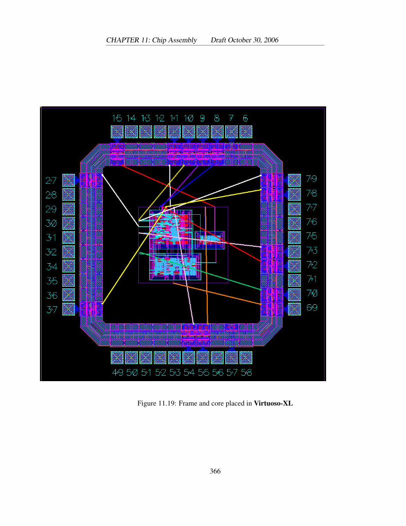
CHAPTER 11: Chip Assembly Draft October 30, 2006
Figure 11.19: Frame and core placed in Virtuoso-XL
366
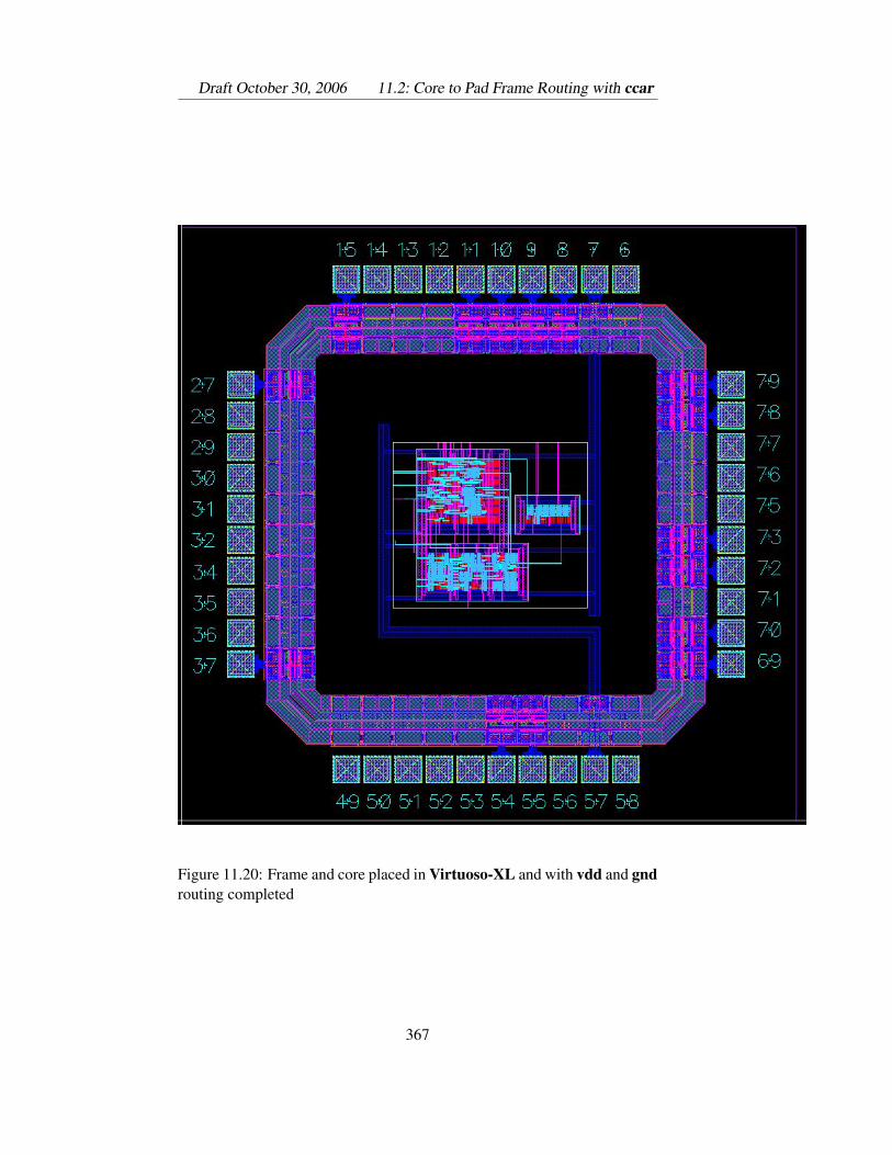
Draft October 30, 2006 11.2: Core to Pad Frame Routing with ccar
Figure 11.20: Frame and core placed in Virtuoso-XL and with vdd and gndrouting completed
367
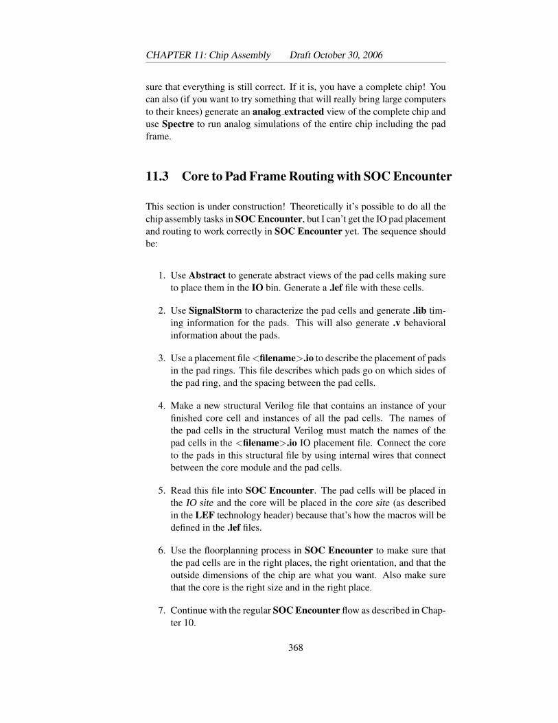
CHAPTER 11: Chip Assembly Draft October 30, 2006
sure that everything is still correct. If it is, you have a complete chip! Youcan also (if you want to try something that will really bring large computersto their knees) generate an analog extracted view of the complete chip anduse Spectre to run analog simulations of the entire chip including the padframe.
11.3 Core to Pad Frame Routing with SOC Encounter
This section is under construction! Theoretically it’s possible to do all thechip assembly tasks in SOC Encounter, but I can’t get the IO pad placementand routing to work correctly in SOC Encounter yet. The sequence shouldbe:
1. Use Abstract to generate abstract views of the pad cells making sureto place them in the IO bin. Generate a .lef file with these cells.
2. Use SignalStorm to characterize the pad cells and generate .lib tim-ing information for the pads. This will also generate .v behavioralinformation about the pads.
3. Use a placement file <filename>.io to describe the placement of padsin the pad rings. This file describes which pads go on which sides ofthe pad ring, and the spacing between the pad cells.
4. Make a new structural Verilog file that contains an instance of yourfinished core cell and instances of all the pad cells. The names ofthe pad cells in the structural Verilog must match the names of thepad cells in the <filename>.io IO placement file. Connect the coreto the pads in this structural file by using internal wires that connectbetween the core module and the pad cells.
5. Read this file into SOC Encounter. The pad cells will be placed inthe IO site and the core will be placed in the core site (as describedin the LEF technology header) because that’s how the macros will bedefined in the .lef files.
6. Use the floorplanning process in SOC Encounter to make sure thatthe pad cells are in the right places, the right orientation, and that theoutside dimensions of the chip are what you want. Also make surethat the core is the right size and in the right place.
7. Continue with the regular SOC Encounter flow as described in Chap-ter 10.
368
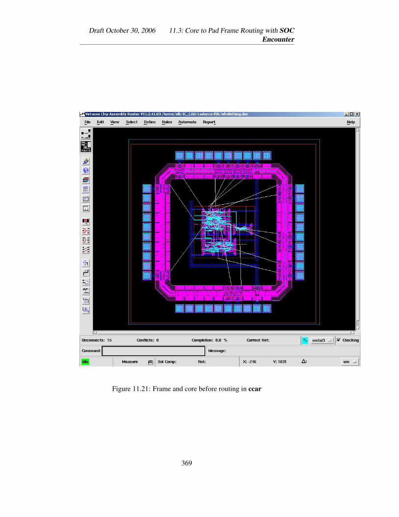
Draft October 30, 2006 11.3: Core to Pad Frame Routing with SOCEncounter
Figure 11.21: Frame and core before routing in ccar
369
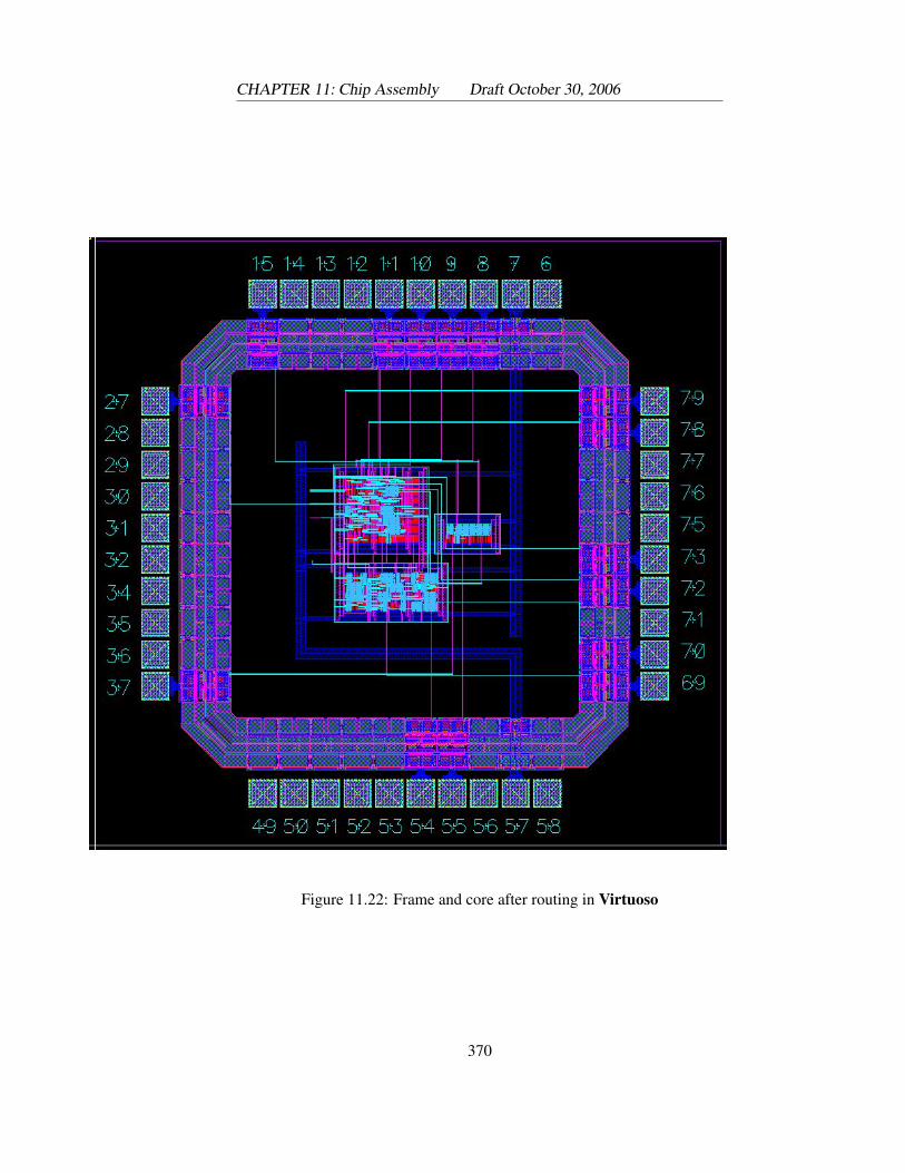
CHAPTER 11: Chip Assembly Draft October 30, 2006
Figure 11.22: Frame and core after routing in Virtuoso
370
Draft October 30, 2006 11.4: Final GDS Generation
This should result in a correctly placed and routed chip. I’ve followedall these steps, but have not yet figured out how to get the SOC Encounterfloorplanning step to correctly place the pads and the core such that every-thing will come out right. Feel free to try this yourself and see if you can getit working if you like. In the meantime, we know that the ccar procedureworks!
11.4 Final GDS Generation
Final Stream (GDS) output - talk about map files, also about metal/poly filland final DRC/LVS on the GDS file
371

CHAPTER 11: Chip Assembly Draft October 30, 2006
372
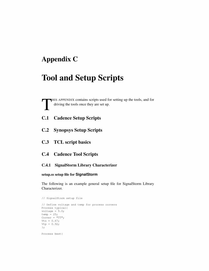
Appendix C
Tool and Setup Scripts
THIS APPENDIX contains scripts used for setting up the tools, and fordriving the tools once they are set up.
C.1 Cadence Setup Scripts
C.2 Synopsys Setup Scripts
C.3 TCL script basics
C.4 Cadence Tool Scripts
C.4.1 SignalStorm Library Characterizer
setup.ss setup file for SignalStorm
The following is an example general setup file for SignalStorm LibraryCharacterizer.
// SignalStorm setup file
// Define voltage and temp for process cornersProcess typical{voltage = 5.0;temp = 25;Corner = "TT";Vtn = 0.67;Vtp = 0.92;};
Process best{
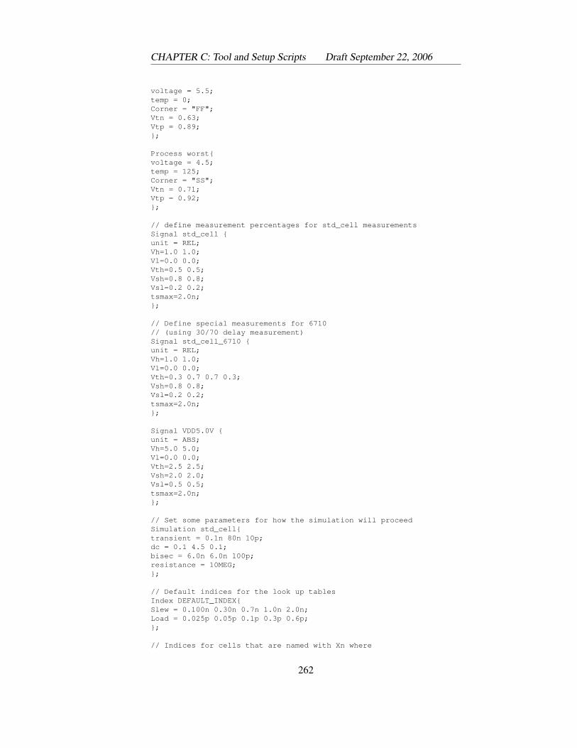
CHAPTER C: Tool and Setup Scripts Draft September 22, 2006
voltage = 5.5;temp = 0;Corner = "FF";Vtn = 0.63;Vtp = 0.89;};
Process worst{voltage = 4.5;temp = 125;Corner = "SS";Vtn = 0.71;Vtp = 0.92;};
// define measurement percentages for std_cell measurementsSignal std_cell {unit = REL;Vh=1.0 1.0;Vl=0.0 0.0;Vth=0.5 0.5;Vsh=0.8 0.8;Vsl=0.2 0.2;tsmax=2.0n;};
// Define special measurements for 6710// (using 30/70 delay measurement)Signal std_cell_6710 {unit = REL;Vh=1.0 1.0;Vl=0.0 0.0;Vth=0.3 0.7 0.7 0.3;Vsh=0.8 0.8;Vsl=0.2 0.2;tsmax=2.0n;};
Signal VDD5.0V {unit = ABS;Vh=5.0 5.0;Vl=0.0 0.0;Vth=2.5 2.5;Vsh=2.0 2.0;Vsl=0.5 0.5;tsmax=2.0n;};
// Set some parameters for how the simulation will proceedSimulation std_cell{transient = 0.1n 80n 10p;dc = 0.1 4.5 0.1;bisec = 6.0n 6.0n 100p;resistance = 10MEG;};
// Default indices for the look up tablesIndex DEFAULT_INDEX{Slew = 0.100n 0.30n 0.7n 1.0n 2.0n;Load = 0.025p 0.05p 0.1p 0.3p 0.6p;};
// Indices for cells that are named with Xn where
262
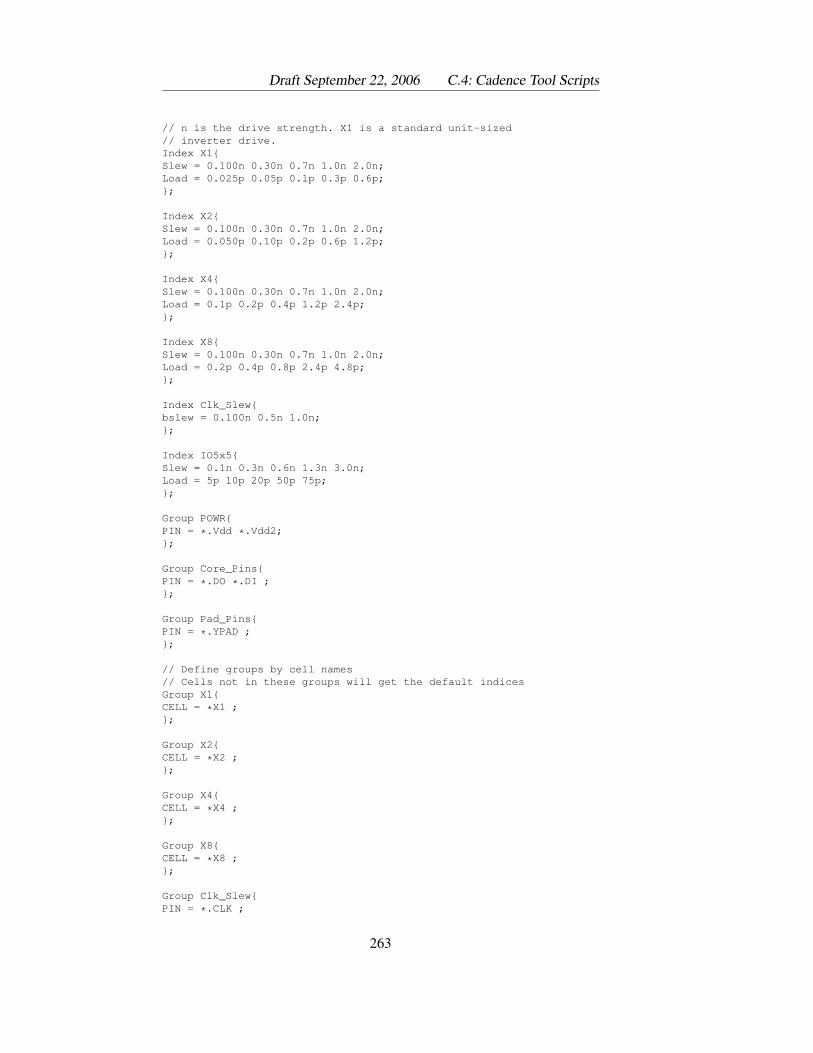
Draft September 22, 2006 C.4: Cadence Tool Scripts
// n is the drive strength. X1 is a standard unit-sized// inverter drive.Index X1{Slew = 0.100n 0.30n 0.7n 1.0n 2.0n;Load = 0.025p 0.05p 0.1p 0.3p 0.6p;};
Index X2{Slew = 0.100n 0.30n 0.7n 1.0n 2.0n;Load = 0.050p 0.10p 0.2p 0.6p 1.2p;};
Index X4{Slew = 0.100n 0.30n 0.7n 1.0n 2.0n;Load = 0.1p 0.2p 0.4p 1.2p 2.4p;};
Index X8{Slew = 0.100n 0.30n 0.7n 1.0n 2.0n;Load = 0.2p 0.4p 0.8p 2.4p 4.8p;};
Index Clk_Slew{bslew = 0.100n 0.5n 1.0n;};
Index IO5x5{Slew = 0.1n 0.3n 0.6n 1.3n 3.0n;Load = 5p 10p 20p 50p 75p;};
Group POWR{PIN = *.Vdd *.Vdd2;};
Group Core_Pins{PIN = *.DO *.DI ;};
Group Pad_Pins{PIN = *.YPAD ;};
// Define groups by cell names// Cells not in these groups will get the default indicesGroup X1{CELL = *X1 ;};
Group X2{CELL = *X2 ;};
Group X4{CELL = *X4 ;};
Group X8{CELL = *X8 ;};
Group Clk_Slew{PIN = *.CLK ;
263
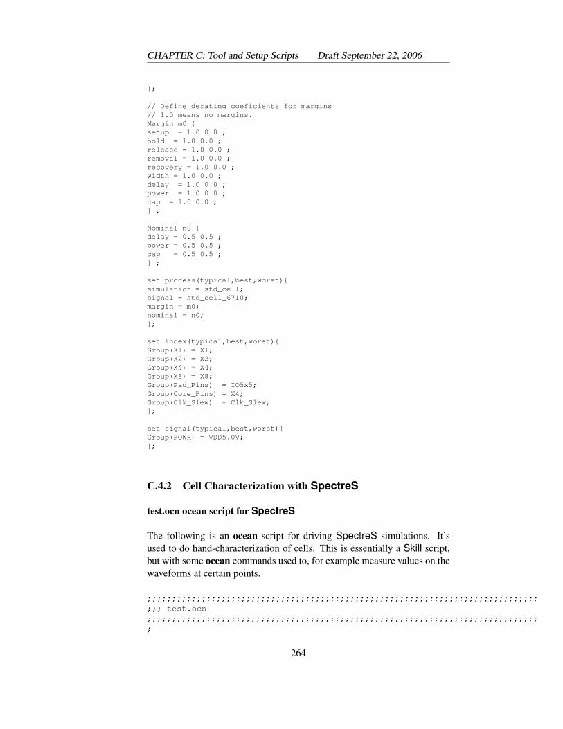
CHAPTER C: Tool and Setup Scripts Draft September 22, 2006
};
// Define derating coeficients for margins// 1.0 means no margins.Margin m0 {setup = 1.0 0.0 ;hold = 1.0 0.0 ;release = 1.0 0.0 ;removal = 1.0 0.0 ;recovery = 1.0 0.0 ;width = 1.0 0.0 ;delay = 1.0 0.0 ;power = 1.0 0.0 ;cap = 1.0 0.0 ;} ;
Nominal n0 {delay = 0.5 0.5 ;power = 0.5 0.5 ;cap = 0.5 0.5 ;} ;
set process(typical,best,worst){simulation = std_cell;signal = std_cell_6710;margin = m0;nominal = n0;};
set index(typical,best,worst){Group(X1) = X1;Group(X2) = X2;Group(X4) = X4;Group(X8) = X8;Group(Pad_Pins) = IO5x5;Group(Core_Pins) = X4;Group(Clk_Slew) = Clk_Slew;};
set signal(typical,best,worst){Group(POWR) = VDD5.0V;};
C.4.2 Cell Characterization with SpectreS
test.ocn ocean script for SpectreS
The following is an ocean script for driving SpectreS simulations. It’sused to do hand-characterization of cells. This is essentially a Skill script,but with some ocean commands used to, for example measure values on thewaveforms at certain points.
;;;;;;;;;;;;;;;;;;;;;;;;;;;;;;;;;;;;;;;;;;;;;;;;;;;;;;;;;;;;;;;;;;;;;;;;;;;;;;;;;; test.ocn;;;;;;;;;;;;;;;;;;;;;;;;;;;;;;;;;;;;;;;;;;;;;;;;;;;;;;;;;;;;;;;;;;;;;;;;;;;;;;;;
264
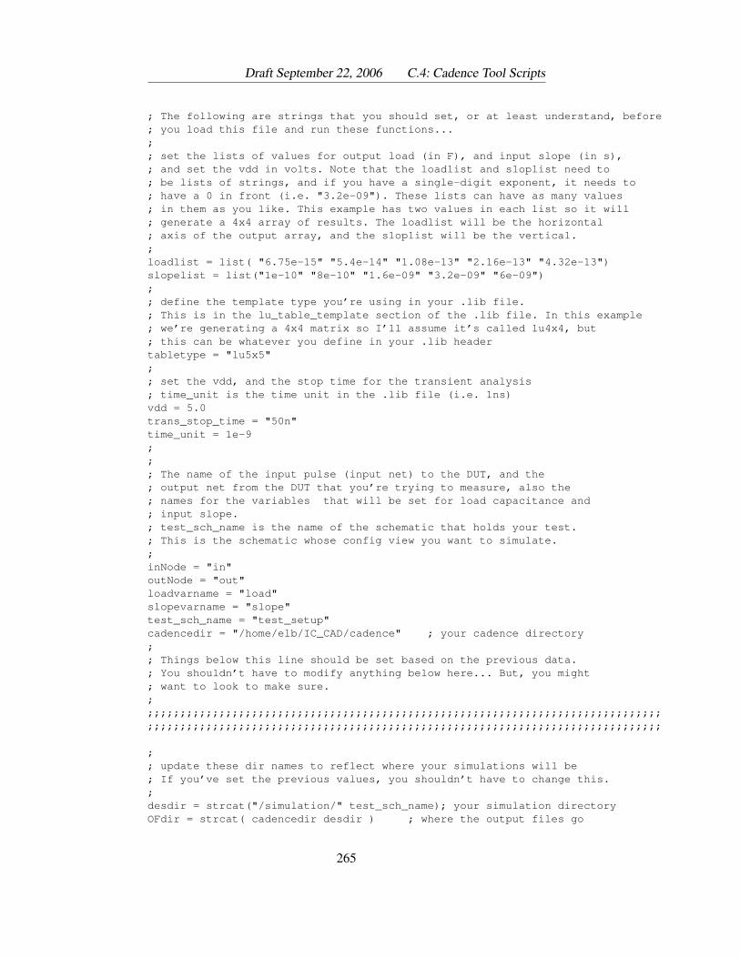
Draft September 22, 2006 C.4: Cadence Tool Scripts
; The following are strings that you should set, or at least understand, before; you load this file and run these functions...;; set the lists of values for output load (in F), and input slope (in s),; and set the vdd in volts. Note that the loadlist and sloplist need to; be lists of strings, and if you have a single-digit exponent, it needs to; have a 0 in front (i.e. "3.2e-09"). These lists can have as many values; in them as you like. This example has two values in each list so it will; generate a 4x4 array of results. The loadlist will be the horizontal; axis of the output array, and the sloplist will be the vertical.;loadlist = list( "6.75e-15" "5.4e-14" "1.08e-13" "2.16e-13" "4.32e-13")slopelist = list("1e-10" "8e-10" "1.6e-09" "3.2e-09" "6e-09");; define the template type you’re using in your .lib file.; This is in the lu_table_template section of the .lib file. In this example; we’re generating a 4x4 matrix so I’ll assume it’s called lu4x4, but; this can be whatever you define in your .lib headertabletype = "lu5x5";; set the vdd, and the stop time for the transient analysis; time_unit is the time unit in the .lib file (i.e. 1ns)vdd = 5.0trans_stop_time = "50n"time_unit = 1e-9;;; The name of the input pulse (input net) to the DUT, and the; output net from the DUT that you’re trying to measure, also the; names for the variables that will be set for load capacitance and; input slope.; test_sch_name is the name of the schematic that holds your test.; This is the schematic whose config view you want to simulate.;inNode = "in"outNode = "out"loadvarname = "load"slopevarname = "slope"test_sch_name = "test_setup"cadencedir = "/home/elb/IC_CAD/cadence" ; your cadence directory;; Things below this line should be set based on the previous data.; You shouldn’t have to modify anything below here... But, you might; want to look to make sure.;;;;;;;;;;;;;;;;;;;;;;;;;;;;;;;;;;;;;;;;;;;;;;;;;;;;;;;;;;;;;;;;;;;;;;;;;;;;;;;;;;;;;;;;;;;;;;;;;;;;;;;;;;;;;;;;;;;;;;;;;;;;;;;;;;;;;;;;;;;;;;;;;;;;;;;;;;;;;;;
;; update these dir names to reflect where your simulations will be; If you’ve set the previous values, you shouldn’t have to change this.;desdir = strcat("/simulation/" test_sch_name); your simulation directoryOFdir = strcat( cadencedir desdir ) ; where the output files go
265
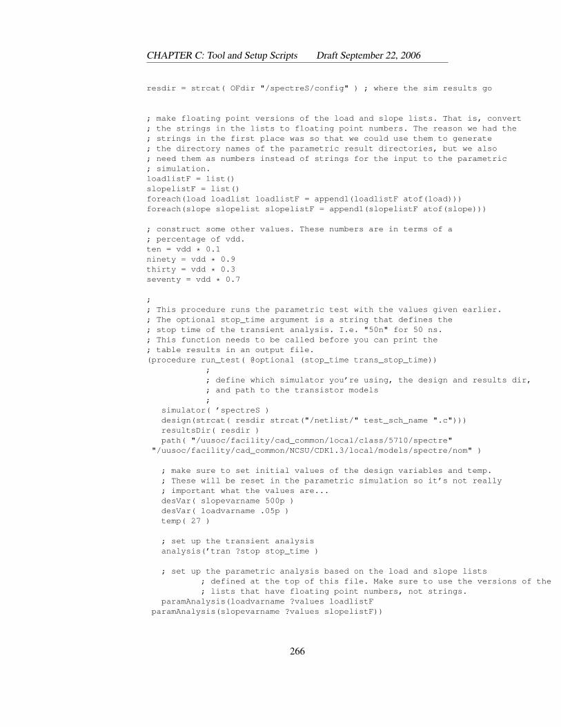
CHAPTER C: Tool and Setup Scripts Draft September 22, 2006
resdir = strcat( OFdir "/spectreS/config" ) ; where the sim results go
; make floating point versions of the load and slope lists. That is, convert; the strings in the lists to floating point numbers. The reason we had the; strings in the first place was so that we could use them to generate; the directory names of the parametric result directories, but we also; need them as numbers instead of strings for the input to the parametric; simulation.loadlistF = list()slopelistF = list()foreach(load loadlist loadlistF = append1(loadlistF atof(load)))foreach(slope slopelist slopelistF = append1(slopelistF atof(slope)))
; construct some other values. These numbers are in terms of a; percentage of vdd.ten = vdd * 0.1ninety = vdd * 0.9thirty = vdd * 0.3seventy = vdd * 0.7
;; This procedure runs the parametric test with the values given earlier.; The optional stop_time argument is a string that defines the; stop time of the transient analysis. I.e. "50n" for 50 ns.; This function needs to be called before you can print the; table results in an output file.(procedure run_test( @optional (stop_time trans_stop_time))
;; define which simulator you’re using, the design and results dir,; and path to the transistor models;
simulator( ’spectreS )design(strcat( resdir strcat("/netlist/" test_sch_name ".c")))resultsDir( resdir )path( "/uusoc/facility/cad_common/local/class/5710/spectre"
"/uusoc/facility/cad_common/NCSU/CDK1.3/local/models/spectre/nom" )
; make sure to set initial values of the design variables and temp.; These will be reset in the parametric simulation so it’s not really; important what the values are...desVar( slopevarname 500p )desVar( loadvarname .05p )temp( 27 )
; set up the transient analysisanalysis(’tran ?stop stop_time )
; set up the parametric analysis based on the load and slope lists; defined at the top of this file. Make sure to use the versions of the; lists that have floating point numbers, not strings.
paramAnalysis(loadvarname ?values loadlistFparamAnalysis(slopevarname ?values slopelistF))
266
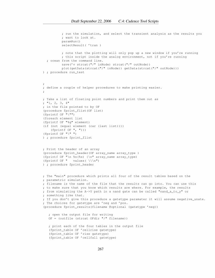
Draft September 22, 2006 C.4: Cadence Tool Scripts
; run the simulation, and select the transient analysis as the results you; want to look at.paramRun()selectResult( ’tran )
; note that the plotting will only pop up a new window if you’re running; this script inside the analog environment, not if you’re running
; ocean from the command line.save(’v strcat("/" inNode) strcat("/" outNode))plot(getData(strcat("/" inNode)) getData(strcat("/" outNode)))
) ; procedure run_test
;; define a couple of helper procedures to make printing easier.;
; Take a list of floating point numbers and print them out as; "1, 2, 3, 4"; in the file pointed to by OF(procedure fprint_flist(OF list)(fprintf OF "\"")(foreach element list(fprintf OF "%g" element)(if (not (equal element (car (last list))))
(fprintf OF ", ")))(fprintf OF "\" ")) ; procedure fprint_flist
; Print the header of an array(procedure fprint_header(OF array_name array_type )(fprintf OF "\n %s(%s) {\n" array_name array_type)(fprintf OF " values( \\\n")) ; procedure fprint_header
; The "main" procedure which prints all four of the result tables based on the; parametric simulation.; filename is the name of the file that the results can go into. You can use this; to make sure that you know which results are where. For example, the results; from simulating the A->Y path in a nand gate can be called "nand_a_to_y" or; something like that.; If you don’t give this procedure a gatetype paramater it will assume negative_unate.; The choices for gatetype are ’neg and ’pos.(procedure fprint_results(filename @optional (gatetype ’neg))
; open the output file for writingOF = (outfile (strcat OFdir "/" filename))
; print each of the four tables in the output file(fprint_table OF ’cellrise gatetype)(fprint_table OF ’rise gatetype)(fprint_table OF ’cellfall gatetype)
267
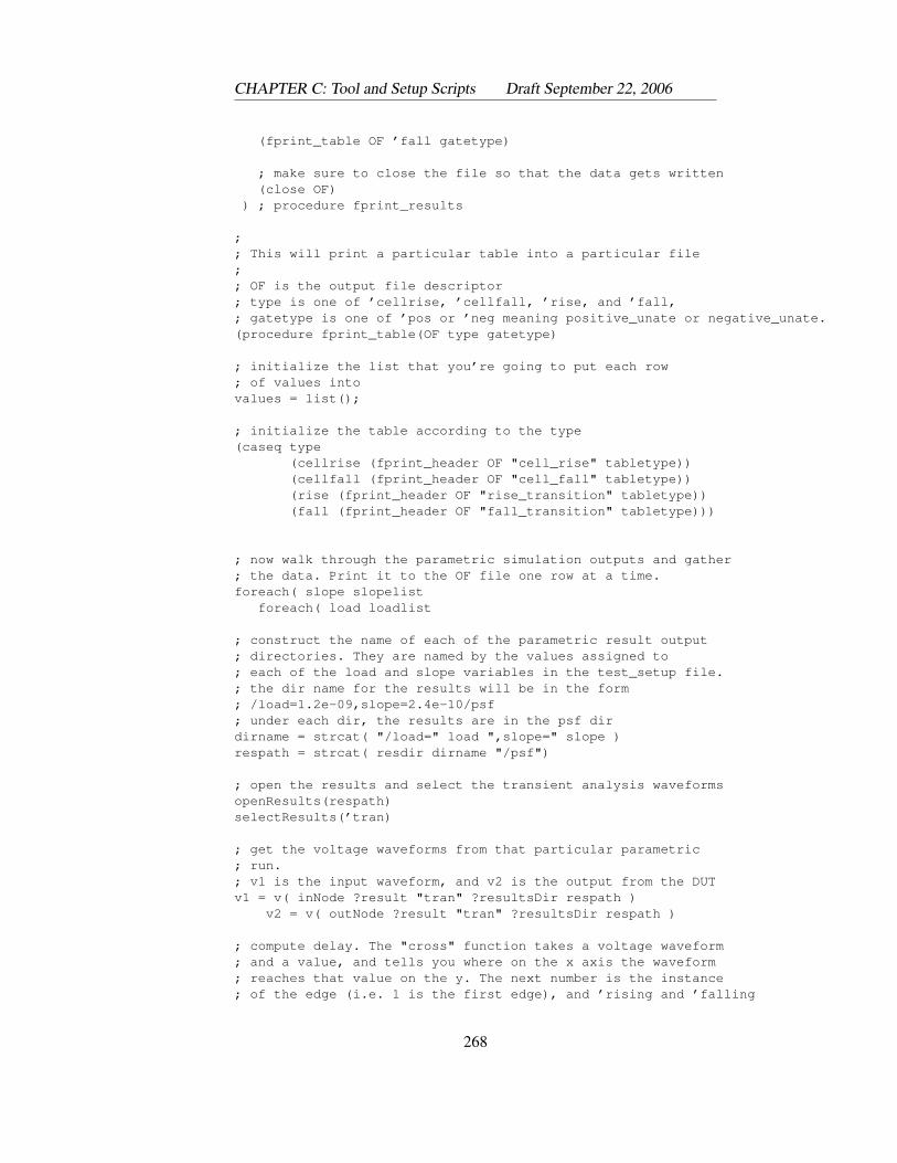
CHAPTER C: Tool and Setup Scripts Draft September 22, 2006
(fprint_table OF ’fall gatetype)
; make sure to close the file so that the data gets written(close OF)
) ; procedure fprint_results
;; This will print a particular table into a particular file;; OF is the output file descriptor; type is one of ’cellrise, ’cellfall, ’rise, and ’fall,; gatetype is one of ’pos or ’neg meaning positive_unate or negative_unate.(procedure fprint_table(OF type gatetype)
; initialize the list that you’re going to put each row; of values intovalues = list();
; initialize the table according to the type(caseq type
(cellrise (fprint_header OF "cell_rise" tabletype))(cellfall (fprint_header OF "cell_fall" tabletype))(rise (fprint_header OF "rise_transition" tabletype))(fall (fprint_header OF "fall_transition" tabletype)))
; now walk through the parametric simulation outputs and gather; the data. Print it to the OF file one row at a time.foreach( slope slopelist
foreach( load loadlist
; construct the name of each of the parametric result output; directories. They are named by the values assigned to; each of the load and slope variables in the test_setup file.; the dir name for the results will be in the form; /load=1.2e-09,slope=2.4e-10/psf; under each dir, the results are in the psf dirdirname = strcat( "/load=" load ",slope=" slope )respath = strcat( resdir dirname "/psf")
; open the results and select the transient analysis waveformsopenResults(respath)selectResults(’tran)
; get the voltage waveforms from that particular parametric; run.; v1 is the input waveform, and v2 is the output from the DUTv1 = v( inNode ?result "tran" ?resultsDir respath )
v2 = v( outNode ?result "tran" ?resultsDir respath )
; compute delay. The "cross" function takes a voltage waveform; and a value, and tells you where on the x axis the waveform; reaches that value on the y. The next number is the instance; of the edge (i.e. 1 is the first edge), and ’rising and ’falling
268
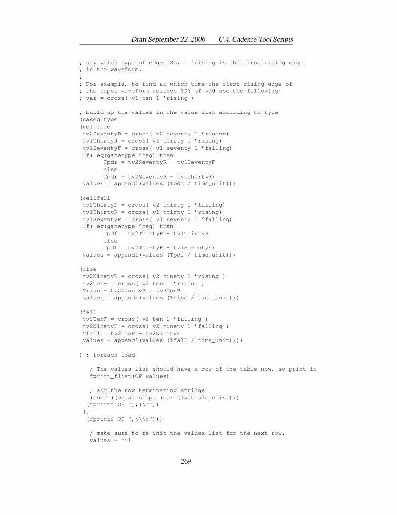
Draft September 22, 2006 C.4: Cadence Tool Scripts
; say which type of edge. So, 1 ’rising is the first rising edge; in the waveform.;; For example, to find at which time the first rising edge of; the input waveform reaches 10% of vdd use the following:; var = cross( v1 ten 1 ’rising )
; build up the values in the value list according to type(caseq type(cellrisetv2SeventyR = cross( v2 seventy 1 ’rising)tv1ThirtyR = cross( v1 thirty 1 ’rising)tv1SeventyF = cross( v1 seventy 1 ’falling)if( eq(gatetype ’neg) then
Tpdr = tv2SeventyR - tv1SeventyFelseTpdr = tv2SeventyR - tv1ThirtyR)
values = append1(values (Tpdr / time_unit)))
(cellfalltv2ThirtyF = cross( v2 thirty 1 ’falling)tv1ThirtyR = cross( v1 thirty 1 ’rising)tv1SeventyF = cross( v1 seventy 1 ’falling)if( eq(gatetype ’neg) then
Tpdf = tv2ThirtyF - tv1ThirtyRelseTpdf = tv2ThirtyF - tv1SeventyF)
values = append1(values (Tpdf / time_unit)))
(risetv2NinetyR = cross( v2 ninety 1 ’rising )tv2TenR = cross( v2 ten 1 ’rising )Trise = tv2NinetyR - tv2TenRvalues = append1(values (Trise / time_unit)))
(falltv2TenF = cross( v2 ten 1 ’falling )tv2NinetyF = cross( v2 ninety 1 ’falling )Tfall = tv2TenF - tv2NinetyFvalues = append1(values (Tfall / time_unit))))
) ; foreach load
; The values list should have a row of the table now, so print itfprint_flist(OF values)
; add the row terminating strings(cond ((equal slope (car (last slopelist)))(fprintf OF ");}\n"))(t(fprintf OF ",\\\n")))
; make sure to re-init the values list for the next row.values = nil
269
CHAPTER C: Tool and Setup Scripts Draft September 22, 2006
) ; foreach slope) ; procedure fprintf_table
;; A "do it all" function that runs the simulation and then generates the results(procedure run_all(filename @optional (gatetype ’neg)(stop_time trans_stop_time))
(run_test stop_time)(fprint_results filename gatetype)
) ; procedure run_all
C.4.3 SOC Encounter
C.4.4 BuildGates Synthesis
C.5 Synopsys Tool Scripts
C.5.1 dc shell Synthesis
C.5.2 Module Compiler Synthesis
C.5.3 PrimeTime Timing Analysis
270
Appendix E
Technology and Cell Libraries
THIS APPENDIX documents the NCSU CDK, the UofU extensions, theUofU Digital library, and the OSU libraries. It also has and exampleof a liberty file for a small example cell library.
E.1 NCSU CDK
E.1.1 UofU Extensions
There are a number of modifications and extentions to the NCSU CDK thatwe use at Utah. These will be documented here.
E.2 Standard Cell Libraries
E.2.1 Example Liberty File
The following is an example of a Liberty file that was generated by Signal-Storm on a small library. The library demonstrates a range of cells includ-ing static combinational cells, tri-state cells, and sequential cells (both flipflops and latches). The cells (shown in the schematic in Figure E.1) are:
dff and dff qb: D-type master slave flip flops. The dff qb varient has bothQ and QB outputs
latch ng iip: A gated latch with negative gate and inverting input
invX1, invX4, invX8: Inverters in a variety of drive strengths
mux2 inv: An inverting 2-way multiplexor
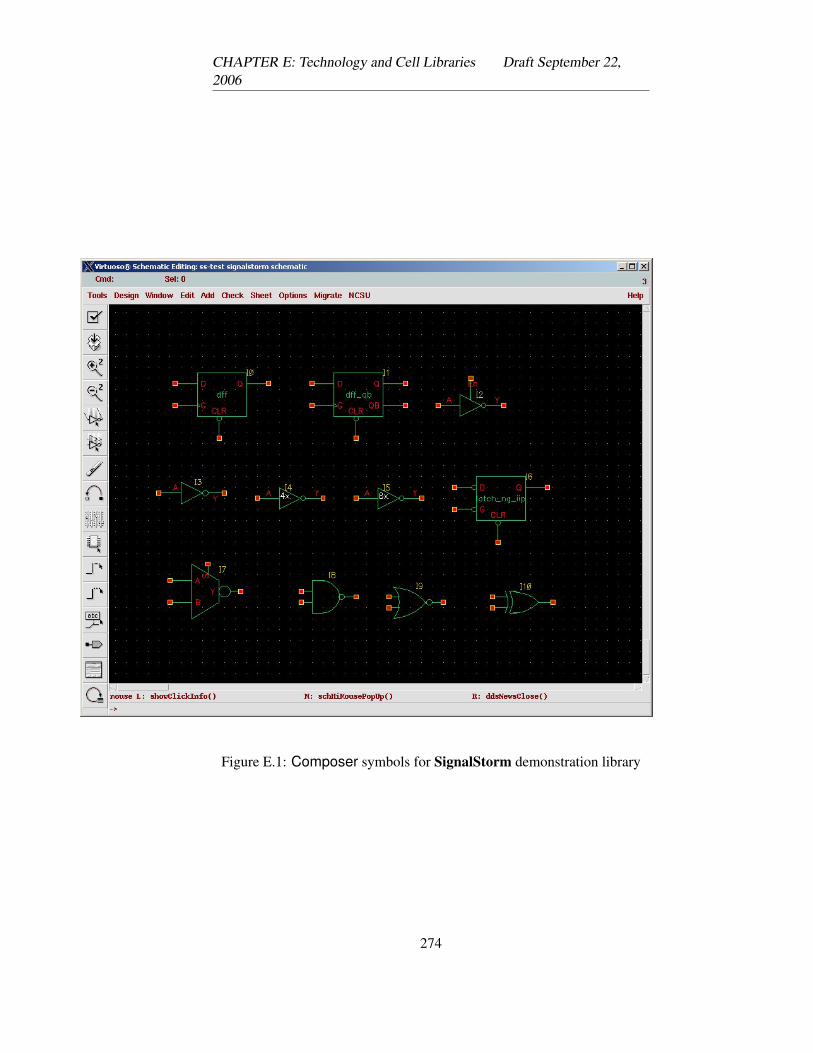
CHAPTER E: Technology and Cell Libraries Draft September 22,2006
Figure E.1: Composer symbols for SignalStorm demonstration library
274
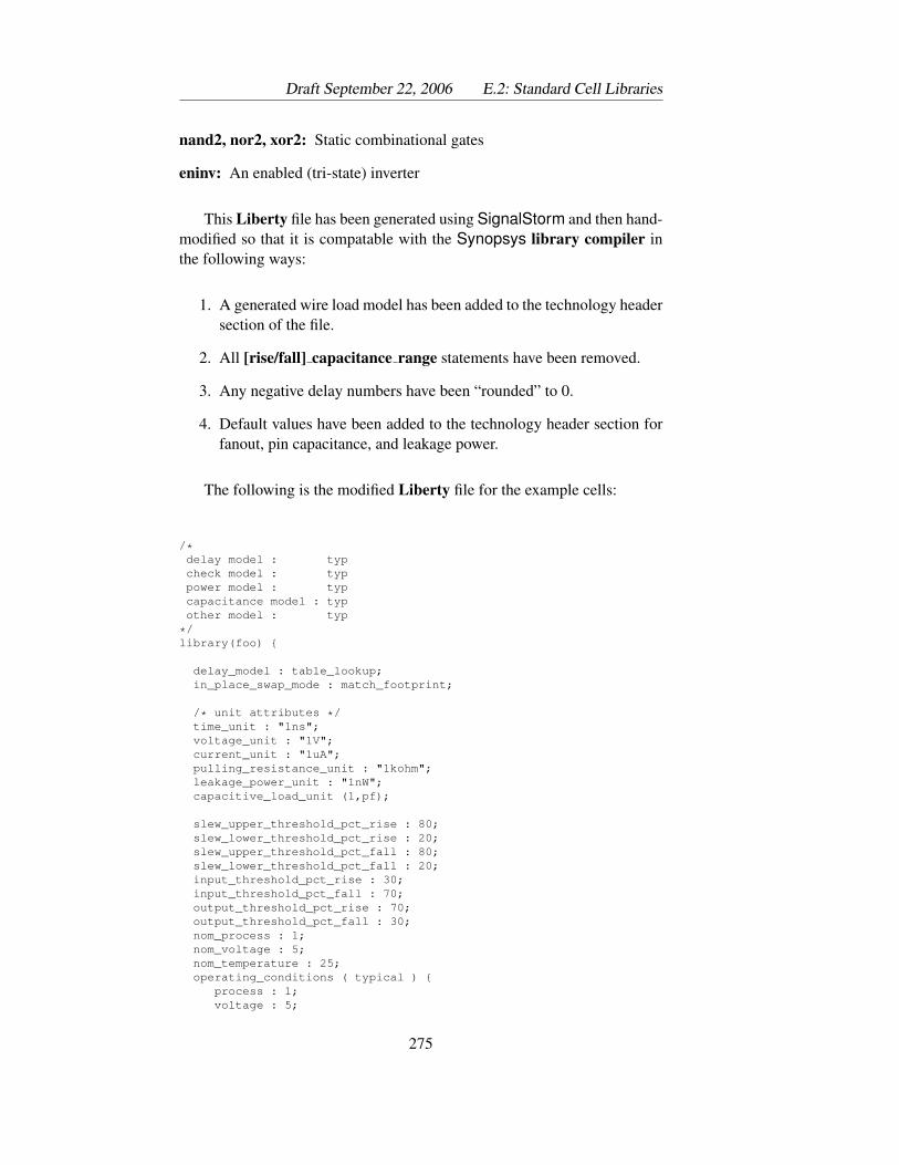
Draft September 22, 2006 E.2: Standard Cell Libraries
nand2, nor2, xor2: Static combinational gates
eninv: An enabled (tri-state) inverter
This Liberty file has been generated using SignalStorm and then hand-modified so that it is compatable with the Synopsys library compiler inthe following ways:
1. A generated wire load model has been added to the technology headersection of the file.
2. All [rise/fall] capacitance range statements have been removed.
3. Any negative delay numbers have been “rounded” to 0.
4. Default values have been added to the technology header section forfanout, pin capacitance, and leakage power.
The following is the modified Liberty file for the example cells:
/*delay model : typcheck model : typpower model : typcapacitance model : typother model : typ
*/library(foo) {
delay_model : table_lookup;in_place_swap_mode : match_footprint;
/* unit attributes */time_unit : "1ns";voltage_unit : "1V";current_unit : "1uA";pulling_resistance_unit : "1kohm";leakage_power_unit : "1nW";capacitive_load_unit (1,pf);
slew_upper_threshold_pct_rise : 80;slew_lower_threshold_pct_rise : 20;slew_upper_threshold_pct_fall : 80;slew_lower_threshold_pct_fall : 20;input_threshold_pct_rise : 30;input_threshold_pct_fall : 70;output_threshold_pct_rise : 70;output_threshold_pct_fall : 30;nom_process : 1;nom_voltage : 5;nom_temperature : 25;operating_conditions ( typical ) {
process : 1;voltage : 5;
275
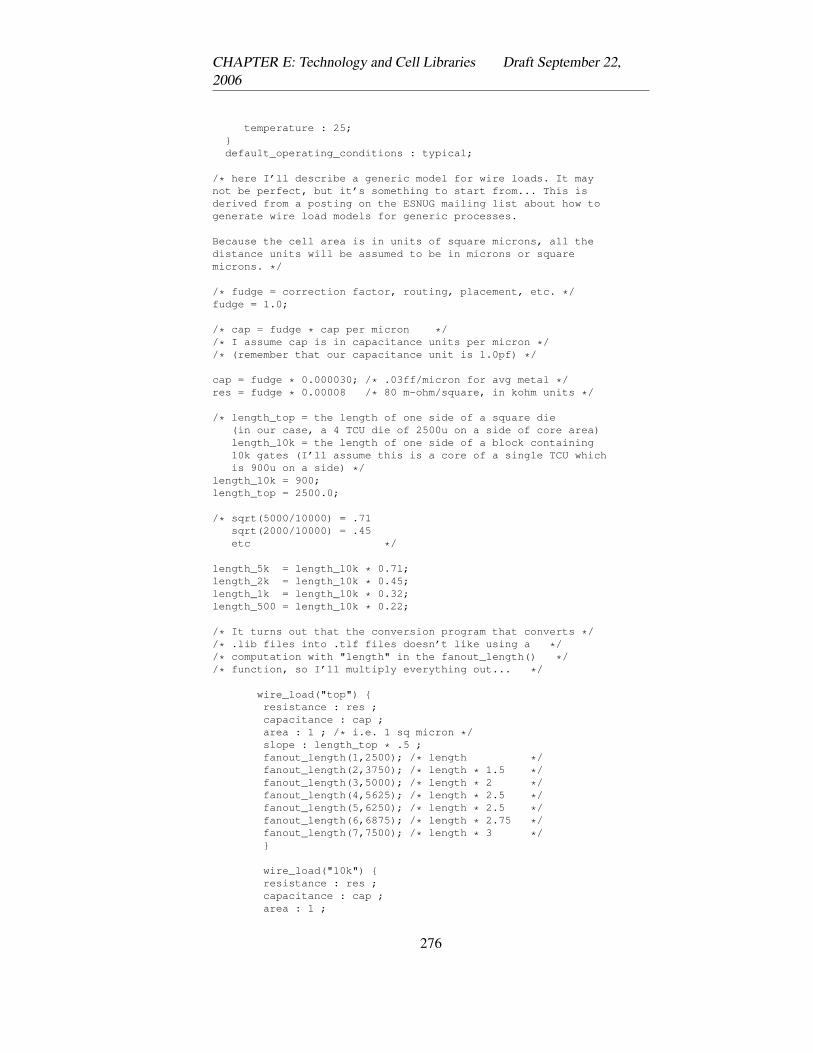
CHAPTER E: Technology and Cell Libraries Draft September 22,2006
temperature : 25;}default_operating_conditions : typical;
/* here I’ll describe a generic model for wire loads. It maynot be perfect, but it’s something to start from... This isderived from a posting on the ESNUG mailing list about how togenerate wire load models for generic processes.
Because the cell area is in units of square microns, all thedistance units will be assumed to be in microns or squaremicrons. */
/* fudge = correction factor, routing, placement, etc. */fudge = 1.0;
/* cap = fudge * cap per micron *//* I assume cap is in capacitance units per micron *//* (remember that our capacitance unit is 1.0pf) */
cap = fudge * 0.000030; /* .03ff/micron for avg metal */res = fudge * 0.00008 /* 80 m-ohm/square, in kohm units */
/* length_top = the length of one side of a square die(in our case, a 4 TCU die of 2500u on a side of core area)length_10k = the length of one side of a block containing10k gates (I’ll assume this is a core of a single TCU whichis 900u on a side) */
length_10k = 900;length_top = 2500.0;
/* sqrt(5000/10000) = .71sqrt(2000/10000) = .45etc */
length_5k = length_10k * 0.71;length_2k = length_10k * 0.45;length_1k = length_10k * 0.32;length_500 = length_10k * 0.22;
/* It turns out that the conversion program that converts *//* .lib files into .tlf files doesn’t like using a *//* computation with "length" in the fanout_length() *//* function, so I’ll multiply everything out... */
wire_load("top") {resistance : res ;capacitance : cap ;area : 1 ; /* i.e. 1 sq micron */slope : length_top * .5 ;fanout_length(1,2500); /* length */fanout_length(2,3750); /* length * 1.5 */fanout_length(3,5000); /* length * 2 */fanout_length(4,5625); /* length * 2.5 */fanout_length(5,6250); /* length * 2.5 */fanout_length(6,6875); /* length * 2.75 */fanout_length(7,7500); /* length * 3 */}
wire_load("10k") {resistance : res ;capacitance : cap ;area : 1 ;
276
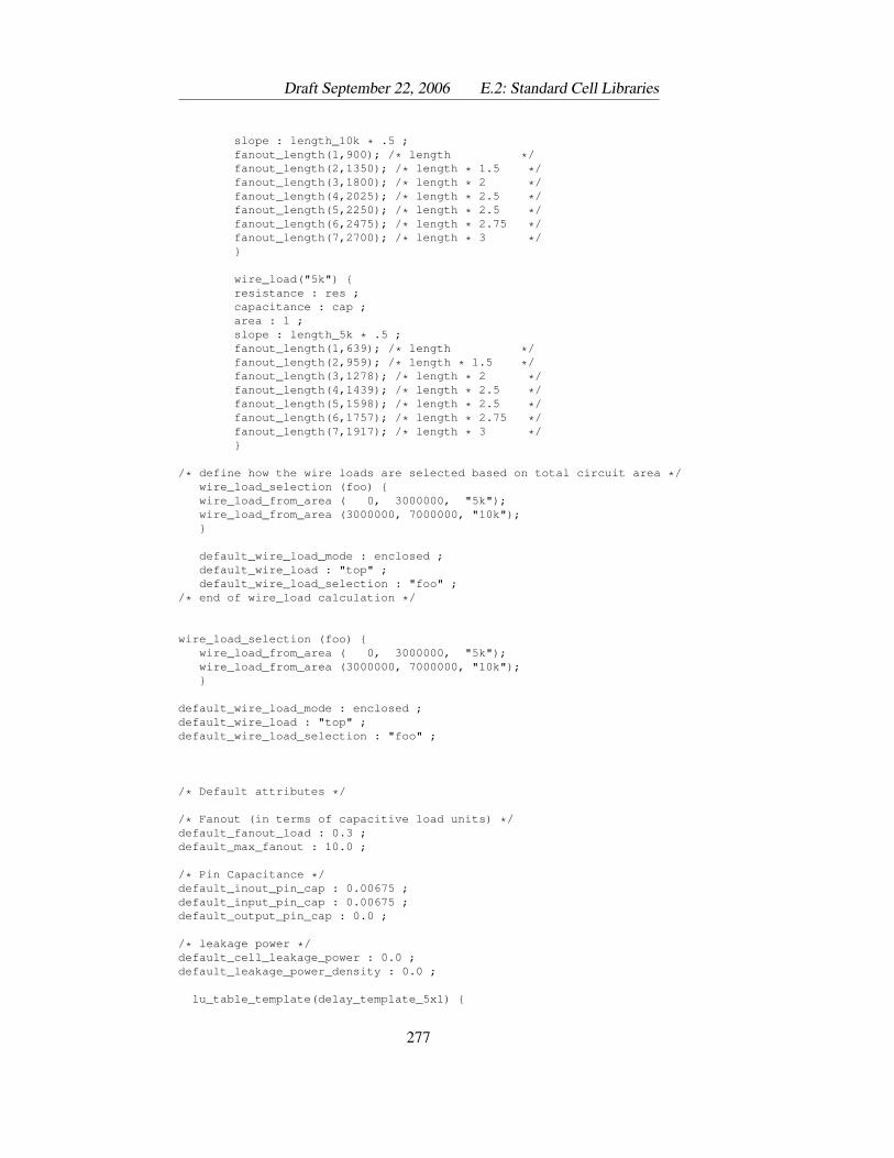
Draft September 22, 2006 E.2: Standard Cell Libraries
slope : length_10k * .5 ;fanout_length(1,900); /* length */fanout_length(2,1350); /* length * 1.5 */fanout_length(3,1800); /* length * 2 */fanout_length(4,2025); /* length * 2.5 */fanout_length(5,2250); /* length * 2.5 */fanout_length(6,2475); /* length * 2.75 */fanout_length(7,2700); /* length * 3 */}
wire_load("5k") {resistance : res ;capacitance : cap ;area : 1 ;slope : length_5k * .5 ;fanout_length(1,639); /* length */fanout_length(2,959); /* length * 1.5 */fanout_length(3,1278); /* length * 2 */fanout_length(4,1439); /* length * 2.5 */fanout_length(5,1598); /* length * 2.5 */fanout_length(6,1757); /* length * 2.75 */fanout_length(7,1917); /* length * 3 */}
/* define how the wire loads are selected based on total circuit area */wire_load_selection (foo) {wire_load_from_area ( 0, 3000000, "5k");wire_load_from_area (3000000, 7000000, "10k");}
default_wire_load_mode : enclosed ;default_wire_load : "top" ;default_wire_load_selection : "foo" ;
/* end of wire_load calculation */
wire_load_selection (foo) {wire_load_from_area ( 0, 3000000, "5k");wire_load_from_area (3000000, 7000000, "10k");}
default_wire_load_mode : enclosed ;default_wire_load : "top" ;default_wire_load_selection : "foo" ;
/* Default attributes */
/* Fanout (in terms of capacitive load units) */default_fanout_load : 0.3 ;default_max_fanout : 10.0 ;
/* Pin Capacitance */default_inout_pin_cap : 0.00675 ;default_input_pin_cap : 0.00675 ;default_output_pin_cap : 0.0 ;
/* leakage power */default_cell_leakage_power : 0.0 ;default_leakage_power_density : 0.0 ;
lu_table_template(delay_template_5x1) {
277
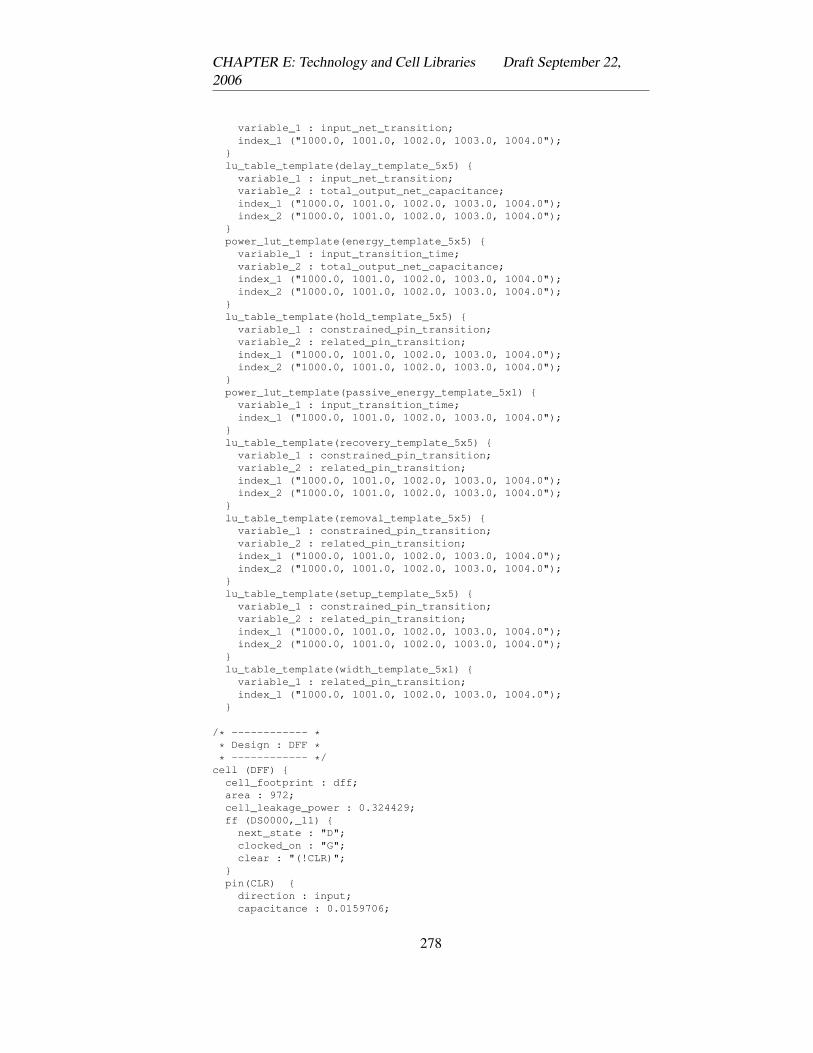
CHAPTER E: Technology and Cell Libraries Draft September 22,2006
variable_1 : input_net_transition;index_1 ("1000.0, 1001.0, 1002.0, 1003.0, 1004.0");
}lu_table_template(delay_template_5x5) {
variable_1 : input_net_transition;variable_2 : total_output_net_capacitance;index_1 ("1000.0, 1001.0, 1002.0, 1003.0, 1004.0");index_2 ("1000.0, 1001.0, 1002.0, 1003.0, 1004.0");
}power_lut_template(energy_template_5x5) {
variable_1 : input_transition_time;variable_2 : total_output_net_capacitance;index_1 ("1000.0, 1001.0, 1002.0, 1003.0, 1004.0");index_2 ("1000.0, 1001.0, 1002.0, 1003.0, 1004.0");
}lu_table_template(hold_template_5x5) {
variable_1 : constrained_pin_transition;variable_2 : related_pin_transition;index_1 ("1000.0, 1001.0, 1002.0, 1003.0, 1004.0");index_2 ("1000.0, 1001.0, 1002.0, 1003.0, 1004.0");
}power_lut_template(passive_energy_template_5x1) {
variable_1 : input_transition_time;index_1 ("1000.0, 1001.0, 1002.0, 1003.0, 1004.0");
}lu_table_template(recovery_template_5x5) {
variable_1 : constrained_pin_transition;variable_2 : related_pin_transition;index_1 ("1000.0, 1001.0, 1002.0, 1003.0, 1004.0");index_2 ("1000.0, 1001.0, 1002.0, 1003.0, 1004.0");
}lu_table_template(removal_template_5x5) {
variable_1 : constrained_pin_transition;variable_2 : related_pin_transition;index_1 ("1000.0, 1001.0, 1002.0, 1003.0, 1004.0");index_2 ("1000.0, 1001.0, 1002.0, 1003.0, 1004.0");
}lu_table_template(setup_template_5x5) {
variable_1 : constrained_pin_transition;variable_2 : related_pin_transition;index_1 ("1000.0, 1001.0, 1002.0, 1003.0, 1004.0");index_2 ("1000.0, 1001.0, 1002.0, 1003.0, 1004.0");
}lu_table_template(width_template_5x1) {
variable_1 : related_pin_transition;index_1 ("1000.0, 1001.0, 1002.0, 1003.0, 1004.0");
}
/* ------------ ** Design : DFF ** ------------ */
cell (DFF) {cell_footprint : dff;area : 972;cell_leakage_power : 0.324429;ff (DS0000,_11) {
next_state : "D";clocked_on : "G";clear : "(!CLR)";
}pin(CLR) {
direction : input;capacitance : 0.0159706;
278
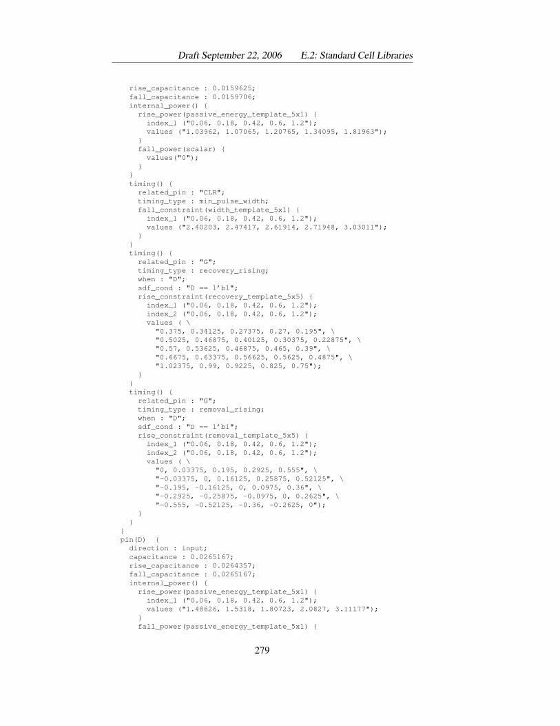
Draft September 22, 2006 E.2: Standard Cell Libraries
rise_capacitance : 0.0159625;fall_capacitance : 0.0159706;internal_power() {
rise_power(passive_energy_template_5x1) {index_1 ("0.06, 0.18, 0.42, 0.6, 1.2");values ("1.03962, 1.07065, 1.20765, 1.34095, 1.81963");
}fall_power(scalar) {
values("0");}
}timing() {
related_pin : "CLR";timing_type : min_pulse_width;fall_constraint(width_template_5x1) {
index_1 ("0.06, 0.18, 0.42, 0.6, 1.2");values ("2.40203, 2.47417, 2.61914, 2.71948, 3.03011");
}}timing() {
related_pin : "G";timing_type : recovery_rising;when : "D";sdf_cond : "D == 1’b1";rise_constraint(recovery_template_5x5) {
index_1 ("0.06, 0.18, 0.42, 0.6, 1.2");index_2 ("0.06, 0.18, 0.42, 0.6, 1.2");values ( \
"0.375, 0.34125, 0.27375, 0.27, 0.195", \"0.5025, 0.46875, 0.40125, 0.30375, 0.22875", \"0.57, 0.53625, 0.46875, 0.465, 0.39", \"0.6675, 0.63375, 0.56625, 0.5625, 0.4875", \"1.02375, 0.99, 0.9225, 0.825, 0.75");
}}timing() {
related_pin : "G";timing_type : removal_rising;when : "D";sdf_cond : "D == 1’b1";rise_constraint(removal_template_5x5) {
index_1 ("0.06, 0.18, 0.42, 0.6, 1.2");index_2 ("0.06, 0.18, 0.42, 0.6, 1.2");values ( \
"0, 0.03375, 0.195, 0.2925, 0.555", \"-0.03375, 0, 0.16125, 0.25875, 0.52125", \"-0.195, -0.16125, 0, 0.0975, 0.36", \"-0.2925, -0.25875, -0.0975, 0, 0.2625", \"-0.555, -0.52125, -0.36, -0.2625, 0");
}}
}pin(D) {
direction : input;capacitance : 0.0265167;rise_capacitance : 0.0264357;fall_capacitance : 0.0265167;internal_power() {
rise_power(passive_energy_template_5x1) {index_1 ("0.06, 0.18, 0.42, 0.6, 1.2");values ("1.48626, 1.5318, 1.80723, 2.0827, 3.11177");
}fall_power(passive_energy_template_5x1) {
279
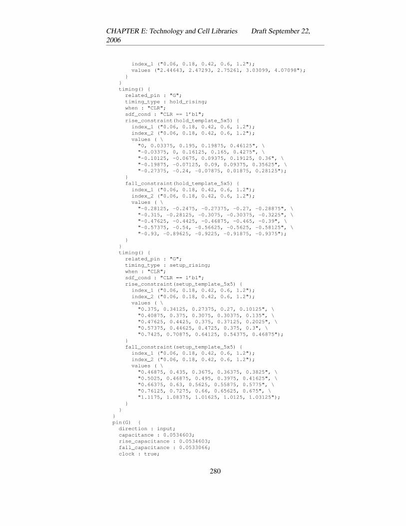
CHAPTER E: Technology and Cell Libraries Draft September 22,2006
index_1 ("0.06, 0.18, 0.42, 0.6, 1.2");values ("2.44643, 2.47293, 2.75261, 3.03099, 4.07098");
}}timing() {
related_pin : "G";timing_type : hold_rising;when : "CLR";sdf_cond : "CLR == 1’b1";rise_constraint(hold_template_5x5) {
index_1 ("0.06, 0.18, 0.42, 0.6, 1.2");index_2 ("0.06, 0.18, 0.42, 0.6, 1.2");values ( \
"0, 0.03375, 0.195, 0.19875, 0.46125", \"-0.03375, 0, 0.16125, 0.165, 0.4275", \"-0.10125, -0.0675, 0.09375, 0.19125, 0.36", \"-0.19875, -0.07125, 0.09, 0.09375, 0.35625", \"-0.27375, -0.24, -0.07875, 0.01875, 0.28125");
}fall_constraint(hold_template_5x5) {
index_1 ("0.06, 0.18, 0.42, 0.6, 1.2");index_2 ("0.06, 0.18, 0.42, 0.6, 1.2");values ( \
"-0.28125, -0.2475, -0.27375, -0.27, -0.28875", \"-0.315, -0.28125, -0.3075, -0.30375, -0.3225", \"-0.47625, -0.4425, -0.46875, -0.465, -0.39", \"-0.57375, -0.54, -0.56625, -0.5625, -0.58125", \"-0.93, -0.89625, -0.9225, -0.91875, -0.9375");
}}timing() {
related_pin : "G";timing_type : setup_rising;when : "CLR";sdf_cond : "CLR == 1’b1";rise_constraint(setup_template_5x5) {
index_1 ("0.06, 0.18, 0.42, 0.6, 1.2");index_2 ("0.06, 0.18, 0.42, 0.6, 1.2");values ( \
"0.375, 0.34125, 0.27375, 0.27, 0.10125", \"0.40875, 0.375, 0.3075, 0.30375, 0.135", \"0.47625, 0.4425, 0.375, 0.37125, 0.2025", \"0.57375, 0.44625, 0.4725, 0.375, 0.3", \"0.7425, 0.70875, 0.64125, 0.54375, 0.46875");
}fall_constraint(setup_template_5x5) {
index_1 ("0.06, 0.18, 0.42, 0.6, 1.2");index_2 ("0.06, 0.18, 0.42, 0.6, 1.2");values ( \
"0.46875, 0.435, 0.3675, 0.36375, 0.3825", \"0.5025, 0.46875, 0.495, 0.3975, 0.41625", \"0.66375, 0.63, 0.5625, 0.55875, 0.5775", \"0.76125, 0.7275, 0.66, 0.65625, 0.675", \"1.1175, 1.08375, 1.01625, 1.0125, 1.03125");
}}
}pin(G) {
direction : input;capacitance : 0.0534603;rise_capacitance : 0.0534603;fall_capacitance : 0.0533066;clock : true;
280
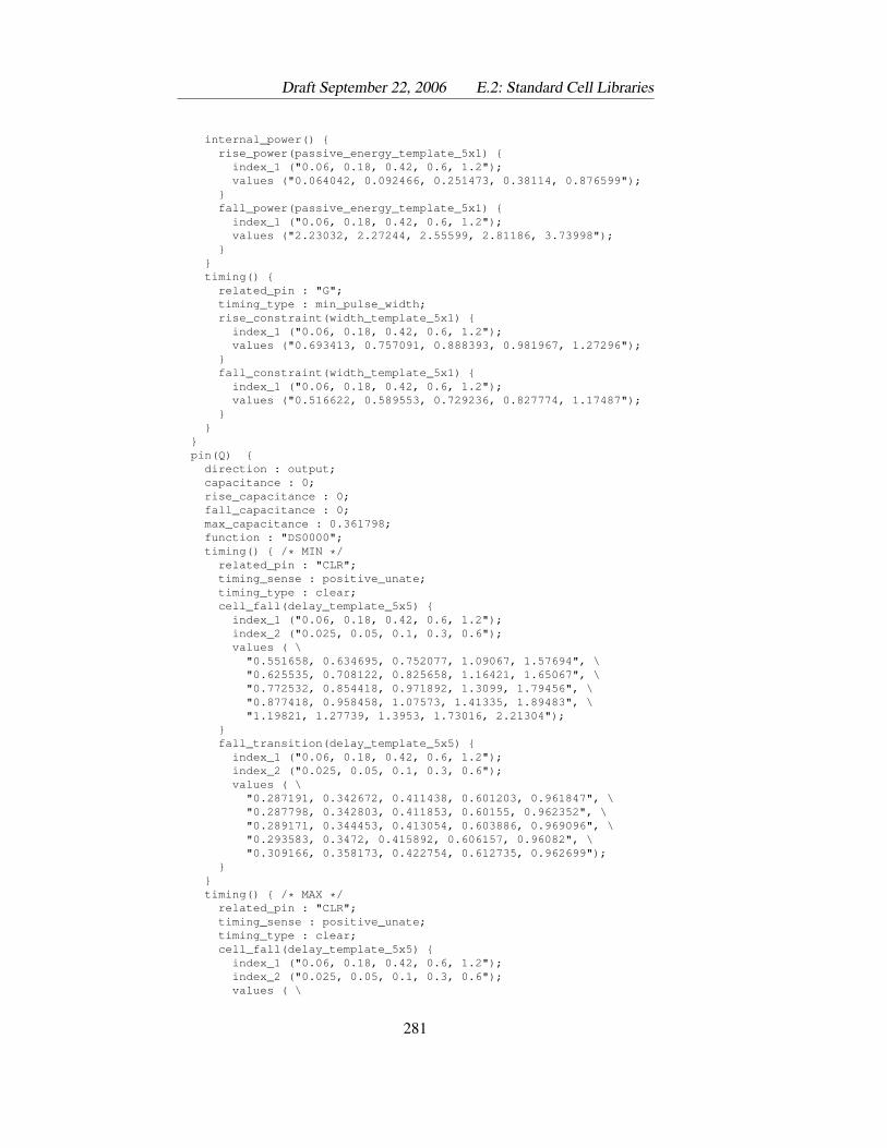
Draft September 22, 2006 E.2: Standard Cell Libraries
internal_power() {rise_power(passive_energy_template_5x1) {
index_1 ("0.06, 0.18, 0.42, 0.6, 1.2");values ("0.064042, 0.092466, 0.251473, 0.38114, 0.876599");
}fall_power(passive_energy_template_5x1) {
index_1 ("0.06, 0.18, 0.42, 0.6, 1.2");values ("2.23032, 2.27244, 2.55599, 2.81186, 3.73998");
}}timing() {
related_pin : "G";timing_type : min_pulse_width;rise_constraint(width_template_5x1) {
index_1 ("0.06, 0.18, 0.42, 0.6, 1.2");values ("0.693413, 0.757091, 0.888393, 0.981967, 1.27296");
}fall_constraint(width_template_5x1) {
index_1 ("0.06, 0.18, 0.42, 0.6, 1.2");values ("0.516622, 0.589553, 0.729236, 0.827774, 1.17487");
}}
}pin(Q) {
direction : output;capacitance : 0;rise_capacitance : 0;fall_capacitance : 0;max_capacitance : 0.361798;function : "DS0000";timing() { /* MIN */
related_pin : "CLR";timing_sense : positive_unate;timing_type : clear;cell_fall(delay_template_5x5) {
index_1 ("0.06, 0.18, 0.42, 0.6, 1.2");index_2 ("0.025, 0.05, 0.1, 0.3, 0.6");values ( \
"0.551658, 0.634695, 0.752077, 1.09067, 1.57694", \"0.625535, 0.708122, 0.825658, 1.16421, 1.65067", \"0.772532, 0.854418, 0.971892, 1.3099, 1.79456", \"0.877418, 0.958458, 1.07573, 1.41335, 1.89483", \"1.19821, 1.27739, 1.3953, 1.73016, 2.21304");
}fall_transition(delay_template_5x5) {
index_1 ("0.06, 0.18, 0.42, 0.6, 1.2");index_2 ("0.025, 0.05, 0.1, 0.3, 0.6");values ( \
"0.287191, 0.342672, 0.411438, 0.601203, 0.961847", \"0.287798, 0.342803, 0.411853, 0.60155, 0.962352", \"0.289171, 0.344453, 0.413054, 0.603886, 0.969096", \"0.293583, 0.3472, 0.415892, 0.606157, 0.96082", \"0.309166, 0.358173, 0.422754, 0.612735, 0.962699");
}}timing() { /* MAX */
related_pin : "CLR";timing_sense : positive_unate;timing_type : clear;cell_fall(delay_template_5x5) {
index_1 ("0.06, 0.18, 0.42, 0.6, 1.2");index_2 ("0.025, 0.05, 0.1, 0.3, 0.6");values ( \
281
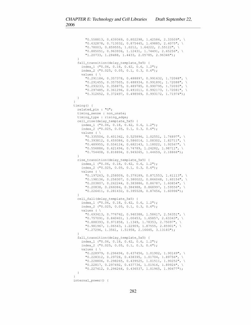
CHAPTER E: Technology and Cell Libraries Draft September 22,2006
"0.558813, 0.639369, 0.802298, 1.42586, 2.33509", \"0.632878, 0.713032, 0.875445, 1.49885, 2.4075", \"0.78003, 0.859555, 1.0212, 1.64222, 2.55122", \"0.885051, 0.963936, 1.12431, 1.74491, 2.65256", \"1.20733, 1.28488, 1.4433, 2.05785, 2.96346");
}fall_transition(delay_template_5x5) {
index_1 ("0.06, 0.18, 0.42, 0.6, 1.2");index_2 ("0.025, 0.05, 0.1, 0.3, 0.6");values ( \
"0.291184, 0.357378, 0.488897, 0.991632, 1.72068", \"0.291455, 0.357505, 0.488934, 0.991891, 1.72088", \"0.293233, 0.358875, 0.489785, 0.990795, 1.72093", \"0.297485, 0.361296, 0.491011, 0.992173, 1.72081", \"0.312652, 0.372497, 0.498569, 0.993172, 1.71974");
}}timing() {
related_pin : "G";timing_sense : non_unate;timing_type : rising_edge;cell_rise(delay_template_5x5) {
index_1 ("0.06, 0.18, 0.42, 0.6, 1.2");index_2 ("0.025, 0.05, 0.1, 0.3, 0.6");values ( \
"0.335504, 0.401342, 0.525896, 1.02551, 1.76897", \"0.393812, 0.459386, 0.586014, 1.08302, 1.82711", \"0.489955, 0.556124, 0.682143, 1.18022, 1.92567", \"0.556886, 0.621494, 0.74789, 1.24282, 1.98711", \"0.754408, 0.818894, 0.949265, 1.44659, 2.18866");
}rise_transition(delay_template_5x5) {
index_1 ("0.06, 0.18, 0.42, 0.6, 1.2");index_2 ("0.025, 0.05, 0.1, 0.3, 0.6");values ( \
"0.197263, 0.258009, 0.379189, 0.871553, 1.61113", \"0.198136, 0.258307, 0.380022, 0.866048, 1.60154", \"0.203807, 0.262244, 0.383886, 0.86787, 1.60854", \"0.20838, 0.266084, 0.384988, 0.868997, 1.59556", \"0.226411, 0.281432, 0.395528, 0.87456, 1.60996");
}cell_fall(delay_template_5x5) {
index_1 ("0.06, 0.18, 0.42, 0.6, 1.2");index_2 ("0.025, 0.05, 0.1, 0.3, 0.6");values ( \
"0.693413, 0.776742, 0.940388, 1.58617, 2.56351", \"0.757091, 0.840401, 1.00453, 1.65857, 2.63343", \"0.888393, 0.971858, 1.1349, 1.78353, 2.75097", \"0.981967, 1.06543, 1.22909, 1.87555, 2.85901", \"1.27296, 1.3561, 1.51958, 2.16645, 3.13183");
}fall_transition(delay_template_5x5) {
index_1 ("0.06, 0.18, 0.42, 0.6, 1.2");index_2 ("0.025, 0.05, 0.1, 0.3, 0.6");values ( \
"0.228979, 0.296494, 0.437456, 1.01902, 1.90149", \"0.228312, 0.29728, 0.438395, 1.01704, 1.89756", \"0.228806, 0.298265, 0.439525, 1.01511, 1.90252", \"0.22817, 0.297492, 0.437736, 1.01916, 1.89924", \"0.227412, 0.296264, 0.436537, 1.01965, 1.90477");
}}internal_power() {
282
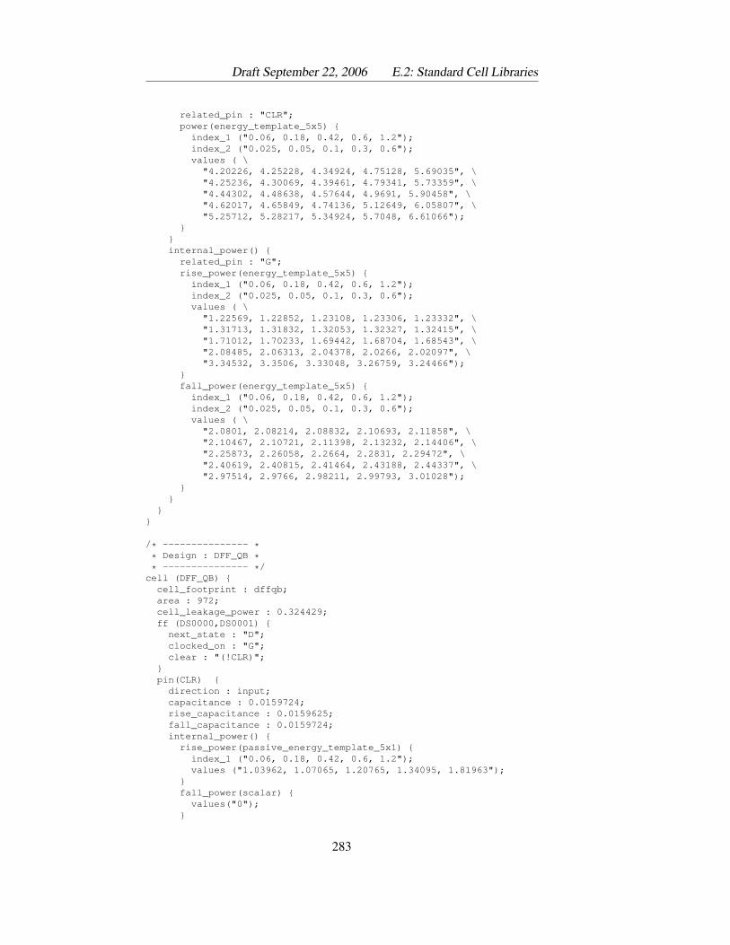
Draft September 22, 2006 E.2: Standard Cell Libraries
related_pin : "CLR";power(energy_template_5x5) {
index_1 ("0.06, 0.18, 0.42, 0.6, 1.2");index_2 ("0.025, 0.05, 0.1, 0.3, 0.6");values ( \
"4.20226, 4.25228, 4.34924, 4.75128, 5.69035", \"4.25236, 4.30069, 4.39461, 4.79341, 5.73359", \"4.44302, 4.48638, 4.57644, 4.9691, 5.90458", \"4.62017, 4.65849, 4.74136, 5.12649, 6.05807", \"5.25712, 5.28217, 5.34924, 5.7048, 6.61066");
}}internal_power() {
related_pin : "G";rise_power(energy_template_5x5) {
index_1 ("0.06, 0.18, 0.42, 0.6, 1.2");index_2 ("0.025, 0.05, 0.1, 0.3, 0.6");values ( \
"1.22569, 1.22852, 1.23108, 1.23306, 1.23332", \"1.31713, 1.31832, 1.32053, 1.32327, 1.32415", \"1.71012, 1.70233, 1.69442, 1.68704, 1.68543", \"2.08485, 2.06313, 2.04378, 2.0266, 2.02097", \"3.34532, 3.3506, 3.33048, 3.26759, 3.24466");
}fall_power(energy_template_5x5) {
index_1 ("0.06, 0.18, 0.42, 0.6, 1.2");index_2 ("0.025, 0.05, 0.1, 0.3, 0.6");values ( \
"2.0801, 2.08214, 2.08832, 2.10693, 2.11858", \"2.10467, 2.10721, 2.11398, 2.13232, 2.14406", \"2.25873, 2.26058, 2.2664, 2.2831, 2.29472", \"2.40619, 2.40815, 2.41464, 2.43188, 2.44337", \"2.97514, 2.9766, 2.98211, 2.99793, 3.01028");
}}
}}
/* --------------- ** Design : DFF_QB ** --------------- */
cell (DFF_QB) {cell_footprint : dffqb;area : 972;cell_leakage_power : 0.324429;ff (DS0000,DS0001) {
next_state : "D";clocked_on : "G";clear : "(!CLR)";
}pin(CLR) {
direction : input;capacitance : 0.0159724;rise_capacitance : 0.0159625;fall_capacitance : 0.0159724;internal_power() {
rise_power(passive_energy_template_5x1) {index_1 ("0.06, 0.18, 0.42, 0.6, 1.2");values ("1.03962, 1.07065, 1.20765, 1.34095, 1.81963");
}fall_power(scalar) {
values("0");}
283
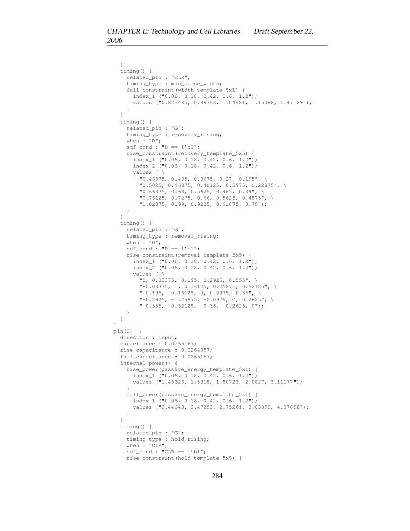
CHAPTER E: Technology and Cell Libraries Draft September 22,2006
}timing() {
related_pin : "CLR";timing_type : min_pulse_width;fall_constraint(width_template_5x1) {
index_1 ("0.06, 0.18, 0.42, 0.6, 1.2");values ("0.823485, 0.89763, 1.04481, 1.15088, 1.47129");
}}timing() {
related_pin : "G";timing_type : recovery_rising;when : "D";sdf_cond : "D == 1’b1";rise_constraint(recovery_template_5x5) {
index_1 ("0.06, 0.18, 0.42, 0.6, 1.2");index_2 ("0.06, 0.18, 0.42, 0.6, 1.2");values ( \
"0.46875, 0.435, 0.3675, 0.27, 0.195", \"0.5025, 0.46875, 0.40125, 0.3975, 0.22875", \"0.66375, 0.63, 0.5625, 0.465, 0.39", \"0.76125, 0.7275, 0.66, 0.5625, 0.4875", \"1.02375, 0.99, 0.9225, 0.91875, 0.75");
}}timing() {
related_pin : "G";timing_type : removal_rising;when : "D";sdf_cond : "D == 1’b1";rise_constraint(removal_template_5x5) {
index_1 ("0.06, 0.18, 0.42, 0.6, 1.2");index_2 ("0.06, 0.18, 0.42, 0.6, 1.2");values ( \
"0, 0.03375, 0.195, 0.2925, 0.555", \"-0.03375, 0, 0.16125, 0.25875, 0.52125", \"-0.195, -0.16125, 0, 0.0975, 0.36", \"-0.2925, -0.25875, -0.0975, 0, 0.2625", \"-0.555, -0.52125, -0.36, -0.2625, 0");
}}
}pin(D) {
direction : input;capacitance : 0.0265167;rise_capacitance : 0.0264357;fall_capacitance : 0.0265167;internal_power() {
rise_power(passive_energy_template_5x1) {index_1 ("0.06, 0.18, 0.42, 0.6, 1.2");values ("1.48626, 1.5318, 1.80723, 2.0827, 3.11177");
}fall_power(passive_energy_template_5x1) {
index_1 ("0.06, 0.18, 0.42, 0.6, 1.2");values ("2.44643, 2.47293, 2.75261, 3.03099, 4.07098");
}}timing() {
related_pin : "G";timing_type : hold_rising;when : "CLR";sdf_cond : "CLR == 1’b1";rise_constraint(hold_template_5x5) {
284
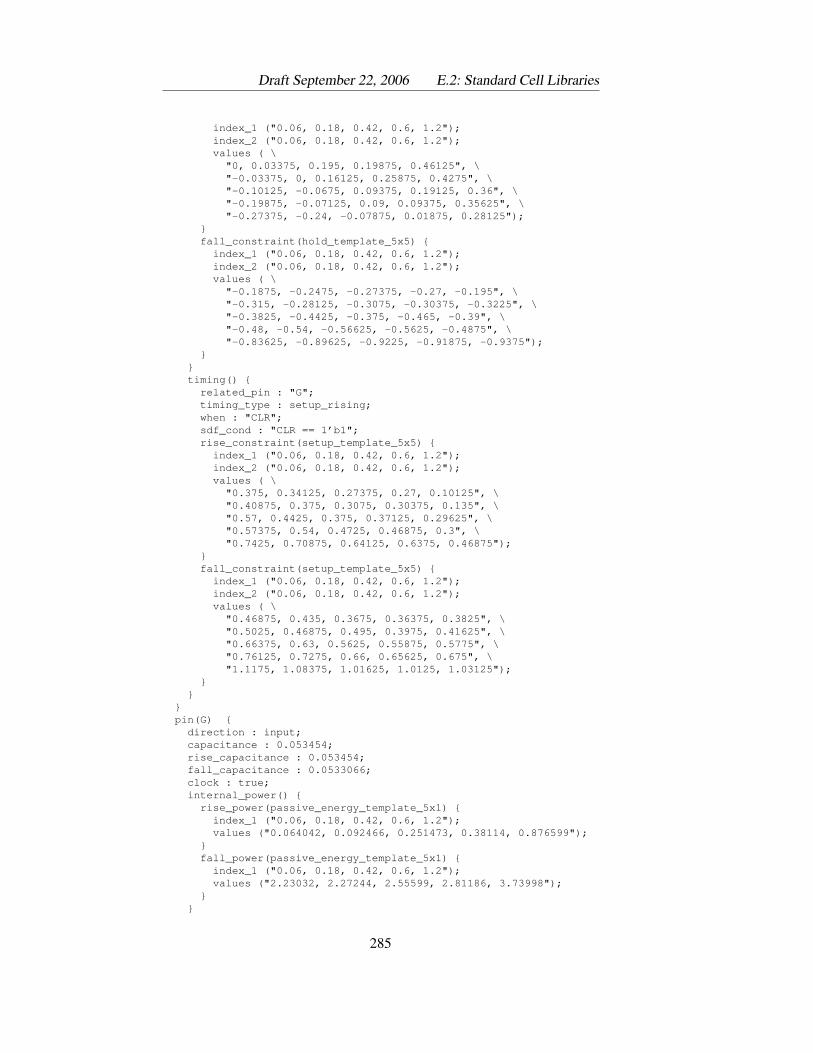
Draft September 22, 2006 E.2: Standard Cell Libraries
index_1 ("0.06, 0.18, 0.42, 0.6, 1.2");index_2 ("0.06, 0.18, 0.42, 0.6, 1.2");values ( \
"0, 0.03375, 0.195, 0.19875, 0.46125", \"-0.03375, 0, 0.16125, 0.25875, 0.4275", \"-0.10125, -0.0675, 0.09375, 0.19125, 0.36", \"-0.19875, -0.07125, 0.09, 0.09375, 0.35625", \"-0.27375, -0.24, -0.07875, 0.01875, 0.28125");
}fall_constraint(hold_template_5x5) {
index_1 ("0.06, 0.18, 0.42, 0.6, 1.2");index_2 ("0.06, 0.18, 0.42, 0.6, 1.2");values ( \
"-0.1875, -0.2475, -0.27375, -0.27, -0.195", \"-0.315, -0.28125, -0.3075, -0.30375, -0.3225", \"-0.3825, -0.4425, -0.375, -0.465, -0.39", \"-0.48, -0.54, -0.56625, -0.5625, -0.4875", \"-0.83625, -0.89625, -0.9225, -0.91875, -0.9375");
}}timing() {
related_pin : "G";timing_type : setup_rising;when : "CLR";sdf_cond : "CLR == 1’b1";rise_constraint(setup_template_5x5) {
index_1 ("0.06, 0.18, 0.42, 0.6, 1.2");index_2 ("0.06, 0.18, 0.42, 0.6, 1.2");values ( \
"0.375, 0.34125, 0.27375, 0.27, 0.10125", \"0.40875, 0.375, 0.3075, 0.30375, 0.135", \"0.57, 0.4425, 0.375, 0.37125, 0.29625", \"0.57375, 0.54, 0.4725, 0.46875, 0.3", \"0.7425, 0.70875, 0.64125, 0.6375, 0.46875");
}fall_constraint(setup_template_5x5) {
index_1 ("0.06, 0.18, 0.42, 0.6, 1.2");index_2 ("0.06, 0.18, 0.42, 0.6, 1.2");values ( \
"0.46875, 0.435, 0.3675, 0.36375, 0.3825", \"0.5025, 0.46875, 0.495, 0.3975, 0.41625", \"0.66375, 0.63, 0.5625, 0.55875, 0.5775", \"0.76125, 0.7275, 0.66, 0.65625, 0.675", \"1.1175, 1.08375, 1.01625, 1.0125, 1.03125");
}}
}pin(G) {
direction : input;capacitance : 0.053454;rise_capacitance : 0.053454;fall_capacitance : 0.0533066;clock : true;internal_power() {
rise_power(passive_energy_template_5x1) {index_1 ("0.06, 0.18, 0.42, 0.6, 1.2");values ("0.064042, 0.092466, 0.251473, 0.38114, 0.876599");
}fall_power(passive_energy_template_5x1) {
index_1 ("0.06, 0.18, 0.42, 0.6, 1.2");values ("2.23032, 2.27244, 2.55599, 2.81186, 3.73998");
}}
285
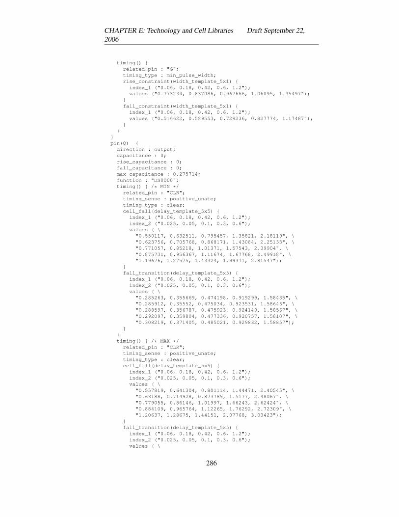
CHAPTER E: Technology and Cell Libraries Draft September 22,2006
timing() {related_pin : "G";timing_type : min_pulse_width;rise_constraint(width_template_5x1) {
index_1 ("0.06, 0.18, 0.42, 0.6, 1.2");values ("0.773234, 0.837086, 0.967666, 1.06095, 1.35497");
}fall_constraint(width_template_5x1) {
index_1 ("0.06, 0.18, 0.42, 0.6, 1.2");values ("0.516622, 0.589553, 0.729236, 0.827774, 1.17487");
}}
}pin(Q) {
direction : output;capacitance : 0;rise_capacitance : 0;fall_capacitance : 0;max_capacitance : 0.275714;function : "DS0000";timing() { /* MIN */
related_pin : "CLR";timing_sense : positive_unate;timing_type : clear;cell_fall(delay_template_5x5) {
index_1 ("0.06, 0.18, 0.42, 0.6, 1.2");index_2 ("0.025, 0.05, 0.1, 0.3, 0.6");values ( \
"0.550117, 0.632511, 0.795457, 1.35821, 2.18119", \"0.623756, 0.705768, 0.868171, 1.43084, 2.25133", \"0.771057, 0.85218, 1.01371, 1.57543, 2.39904", \"0.875731, 0.956367, 1.11674, 1.67768, 2.49918", \"1.19676, 1.27575, 1.43324, 1.99371, 2.81547");
}fall_transition(delay_template_5x5) {
index_1 ("0.06, 0.18, 0.42, 0.6, 1.2");index_2 ("0.025, 0.05, 0.1, 0.3, 0.6");values ( \
"0.285263, 0.355669, 0.474198, 0.919299, 1.58435", \"0.285912, 0.35552, 0.475034, 0.923531, 1.58646", \"0.288597, 0.356787, 0.475923, 0.924149, 1.58567", \"0.292097, 0.359804, 0.477336, 0.920757, 1.58107", \"0.308219, 0.371405, 0.485021, 0.929832, 1.58857");
}}timing() { /* MAX */
related_pin : "CLR";timing_sense : positive_unate;timing_type : clear;cell_fall(delay_template_5x5) {
index_1 ("0.06, 0.18, 0.42, 0.6, 1.2");index_2 ("0.025, 0.05, 0.1, 0.3, 0.6");values ( \
"0.557819, 0.641304, 0.801114, 1.44471, 2.40545", \"0.63188, 0.714928, 0.873789, 1.5177, 2.48067", \"0.779055, 0.86146, 1.01997, 1.66243, 2.62424", \"0.884109, 0.965764, 1.12265, 1.76292, 2.72309", \"1.20637, 1.28675, 1.44151, 2.07768, 3.03423");
}fall_transition(delay_template_5x5) {
index_1 ("0.06, 0.18, 0.42, 0.6, 1.2");index_2 ("0.025, 0.05, 0.1, 0.3, 0.6");values ( \
286
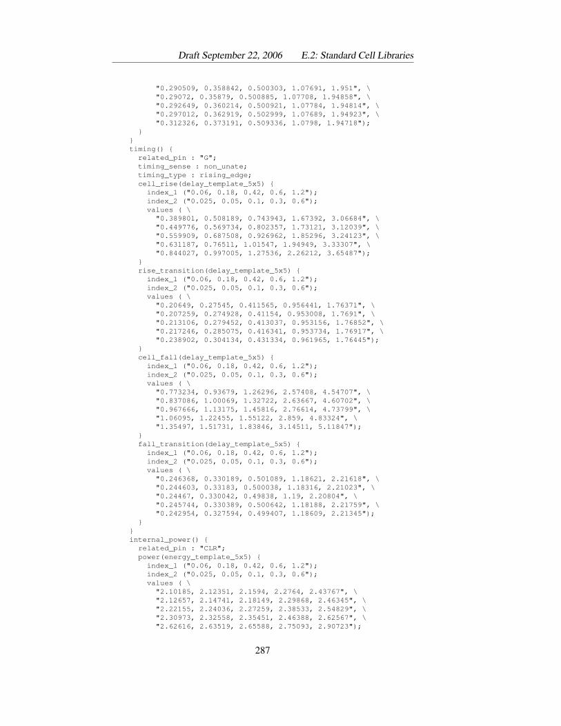
Draft September 22, 2006 E.2: Standard Cell Libraries
"0.290509, 0.358842, 0.500303, 1.07691, 1.951", \"0.29072, 0.35879, 0.500885, 1.07708, 1.94858", \"0.292649, 0.360214, 0.500921, 1.07784, 1.94814", \"0.297012, 0.362919, 0.502999, 1.07689, 1.94923", \"0.312326, 0.373191, 0.509336, 1.0798, 1.94718");
}}timing() {
related_pin : "G";timing_sense : non_unate;timing_type : rising_edge;cell_rise(delay_template_5x5) {
index_1 ("0.06, 0.18, 0.42, 0.6, 1.2");index_2 ("0.025, 0.05, 0.1, 0.3, 0.6");values ( \
"0.389801, 0.508189, 0.743943, 1.67392, 3.06684", \"0.449776, 0.569734, 0.802357, 1.73121, 3.12039", \"0.559909, 0.687508, 0.926962, 1.85296, 3.24123", \"0.631187, 0.76511, 1.01547, 1.94949, 3.33307", \"0.844027, 0.997005, 1.27536, 2.26212, 3.65487");
}rise_transition(delay_template_5x5) {
index_1 ("0.06, 0.18, 0.42, 0.6, 1.2");index_2 ("0.025, 0.05, 0.1, 0.3, 0.6");values ( \
"0.20649, 0.27545, 0.411565, 0.956441, 1.76371", \"0.207259, 0.274928, 0.41154, 0.953008, 1.7691", \"0.213106, 0.279452, 0.413037, 0.953156, 1.76852", \"0.217246, 0.285075, 0.416341, 0.953734, 1.76917", \"0.238902, 0.304134, 0.431334, 0.961965, 1.76445");
}cell_fall(delay_template_5x5) {
index_1 ("0.06, 0.18, 0.42, 0.6, 1.2");index_2 ("0.025, 0.05, 0.1, 0.3, 0.6");values ( \
"0.773234, 0.93679, 1.26296, 2.57408, 4.54707", \"0.837086, 1.00069, 1.32722, 2.63667, 4.60702", \"0.967666, 1.13175, 1.45816, 2.76614, 4.73799", \"1.06095, 1.22455, 1.55122, 2.859, 4.83324", \"1.35497, 1.51731, 1.83846, 3.14511, 5.11847");
}fall_transition(delay_template_5x5) {
index_1 ("0.06, 0.18, 0.42, 0.6, 1.2");index_2 ("0.025, 0.05, 0.1, 0.3, 0.6");values ( \
"0.246368, 0.330189, 0.501089, 1.18621, 2.21618", \"0.244603, 0.33183, 0.500038, 1.18316, 2.21023", \"0.24467, 0.330042, 0.49838, 1.19, 2.20804", \"0.245744, 0.330389, 0.500642, 1.18188, 2.21759", \"0.242954, 0.327594, 0.499407, 1.18609, 2.21345");
}}internal_power() {
related_pin : "CLR";power(energy_template_5x5) {
index_1 ("0.06, 0.18, 0.42, 0.6, 1.2");index_2 ("0.025, 0.05, 0.1, 0.3, 0.6");values ( \
"2.10185, 2.12351, 2.1594, 2.2764, 2.43767", \"2.12657, 2.14741, 2.18149, 2.29868, 2.46345", \"2.22155, 2.24036, 2.27259, 2.38533, 2.54829", \"2.30973, 2.32558, 2.35451, 2.46388, 2.62567", \"2.62616, 2.63519, 2.65588, 2.75093, 2.90723");
287
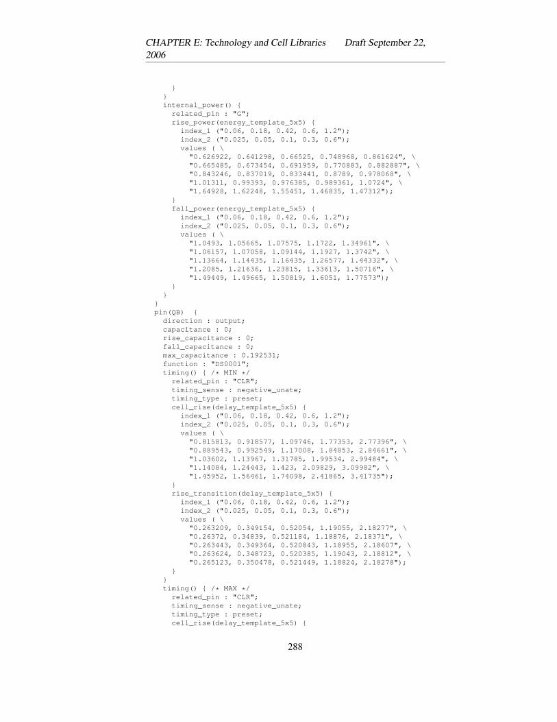
CHAPTER E: Technology and Cell Libraries Draft September 22,2006
}}internal_power() {
related_pin : "G";rise_power(energy_template_5x5) {
index_1 ("0.06, 0.18, 0.42, 0.6, 1.2");index_2 ("0.025, 0.05, 0.1, 0.3, 0.6");values ( \
"0.626922, 0.641298, 0.66525, 0.748968, 0.861624", \"0.665485, 0.673454, 0.691959, 0.770883, 0.882887", \"0.843246, 0.837019, 0.833441, 0.8789, 0.978068", \"1.01311, 0.99393, 0.976385, 0.989361, 1.0724", \"1.64928, 1.62248, 1.55451, 1.46835, 1.47312");
}fall_power(energy_template_5x5) {
index_1 ("0.06, 0.18, 0.42, 0.6, 1.2");index_2 ("0.025, 0.05, 0.1, 0.3, 0.6");values ( \
"1.0493, 1.05665, 1.07575, 1.1722, 1.34961", \"1.06157, 1.07058, 1.09144, 1.1927, 1.3742", \"1.13664, 1.14435, 1.16435, 1.26577, 1.44332", \"1.2085, 1.21636, 1.23815, 1.33613, 1.50716", \"1.49449, 1.49665, 1.50819, 1.6051, 1.77573");
}}
}pin(QB) {
direction : output;capacitance : 0;rise_capacitance : 0;fall_capacitance : 0;max_capacitance : 0.192531;function : "DS0001";timing() { /* MIN */
related_pin : "CLR";timing_sense : negative_unate;timing_type : preset;cell_rise(delay_template_5x5) {
index_1 ("0.06, 0.18, 0.42, 0.6, 1.2");index_2 ("0.025, 0.05, 0.1, 0.3, 0.6");values ( \
"0.815813, 0.918577, 1.09746, 1.77353, 2.77396", \"0.889543, 0.992549, 1.17008, 1.84853, 2.84661", \"1.03602, 1.13967, 1.31785, 1.99534, 2.99484", \"1.14084, 1.24443, 1.423, 2.09829, 3.09982", \"1.45952, 1.56461, 1.74098, 2.41865, 3.41735");
}rise_transition(delay_template_5x5) {
index_1 ("0.06, 0.18, 0.42, 0.6, 1.2");index_2 ("0.025, 0.05, 0.1, 0.3, 0.6");values ( \
"0.263209, 0.349154, 0.52054, 1.19055, 2.18277", \"0.26372, 0.34839, 0.521184, 1.18876, 2.18371", \"0.263443, 0.349364, 0.520843, 1.18955, 2.18607", \"0.263624, 0.348723, 0.520385, 1.19043, 2.18812", \"0.265123, 0.350478, 0.521449, 1.18824, 2.18278");
}}timing() { /* MAX */
related_pin : "CLR";timing_sense : negative_unate;timing_type : preset;cell_rise(delay_template_5x5) {
288
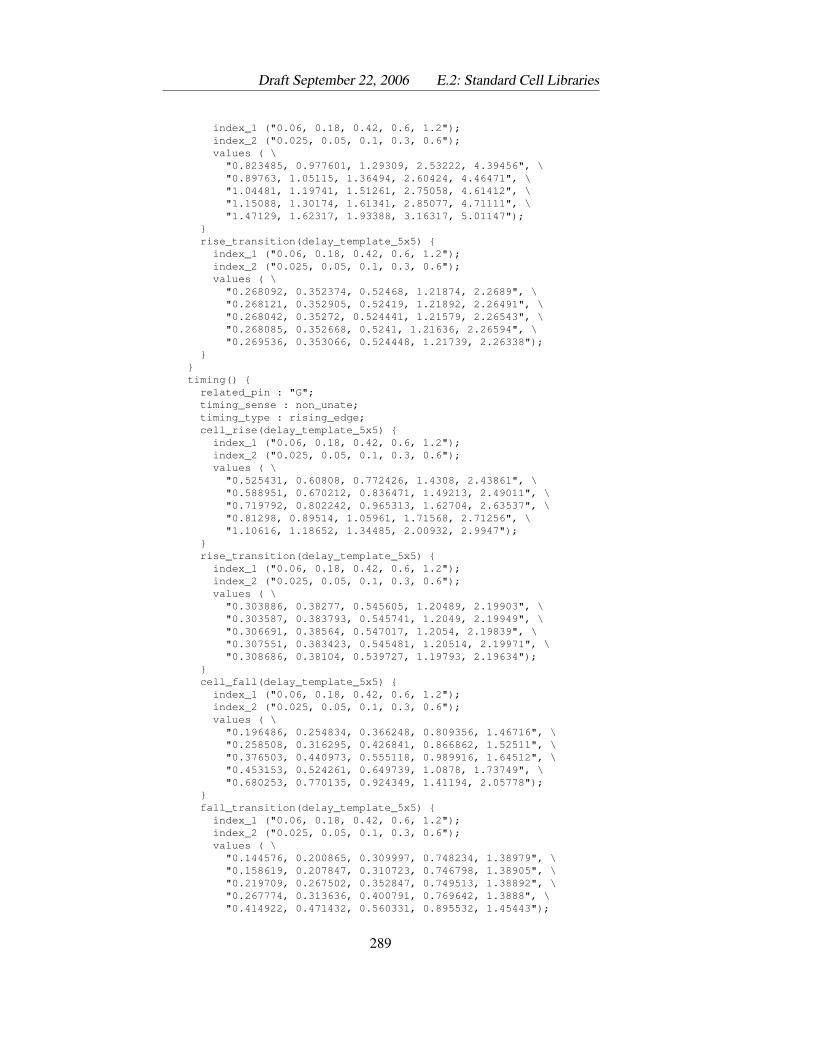
Draft September 22, 2006 E.2: Standard Cell Libraries
index_1 ("0.06, 0.18, 0.42, 0.6, 1.2");index_2 ("0.025, 0.05, 0.1, 0.3, 0.6");values ( \
"0.823485, 0.977601, 1.29309, 2.53222, 4.39456", \"0.89763, 1.05115, 1.36494, 2.60424, 4.46471", \"1.04481, 1.19741, 1.51261, 2.75058, 4.61412", \"1.15088, 1.30174, 1.61341, 2.85077, 4.71111", \"1.47129, 1.62317, 1.93388, 3.16317, 5.01147");
}rise_transition(delay_template_5x5) {
index_1 ("0.06, 0.18, 0.42, 0.6, 1.2");index_2 ("0.025, 0.05, 0.1, 0.3, 0.6");values ( \
"0.268092, 0.352374, 0.52468, 1.21874, 2.2689", \"0.268121, 0.352905, 0.52419, 1.21892, 2.26491", \"0.268042, 0.35272, 0.524441, 1.21579, 2.26543", \"0.268085, 0.352668, 0.5241, 1.21636, 2.26594", \"0.269536, 0.353066, 0.524448, 1.21739, 2.26338");
}}timing() {
related_pin : "G";timing_sense : non_unate;timing_type : rising_edge;cell_rise(delay_template_5x5) {
index_1 ("0.06, 0.18, 0.42, 0.6, 1.2");index_2 ("0.025, 0.05, 0.1, 0.3, 0.6");values ( \
"0.525431, 0.60808, 0.772426, 1.4308, 2.43861", \"0.588951, 0.670212, 0.836471, 1.49213, 2.49011", \"0.719792, 0.802242, 0.965313, 1.62704, 2.63537", \"0.81298, 0.89514, 1.05961, 1.71568, 2.71256", \"1.10616, 1.18652, 1.34485, 2.00932, 2.9947");
}rise_transition(delay_template_5x5) {
index_1 ("0.06, 0.18, 0.42, 0.6, 1.2");index_2 ("0.025, 0.05, 0.1, 0.3, 0.6");values ( \
"0.303886, 0.38277, 0.545605, 1.20489, 2.19903", \"0.303587, 0.383793, 0.545741, 1.2049, 2.19949", \"0.306691, 0.38564, 0.547017, 1.2054, 2.19839", \"0.307551, 0.383423, 0.545481, 1.20514, 2.19971", \"0.308686, 0.38104, 0.539727, 1.19793, 2.19634");
}cell_fall(delay_template_5x5) {
index_1 ("0.06, 0.18, 0.42, 0.6, 1.2");index_2 ("0.025, 0.05, 0.1, 0.3, 0.6");values ( \
"0.196486, 0.254834, 0.366248, 0.809356, 1.46716", \"0.258508, 0.316295, 0.426841, 0.866862, 1.52511", \"0.376503, 0.440973, 0.555118, 0.989916, 1.64512", \"0.453153, 0.524261, 0.649739, 1.0878, 1.73749", \"0.680253, 0.770135, 0.924349, 1.41194, 2.05778");
}fall_transition(delay_template_5x5) {
index_1 ("0.06, 0.18, 0.42, 0.6, 1.2");index_2 ("0.025, 0.05, 0.1, 0.3, 0.6");values ( \
"0.144576, 0.200865, 0.309997, 0.748234, 1.38979", \"0.158619, 0.207847, 0.310723, 0.746798, 1.38905", \"0.219709, 0.267502, 0.352847, 0.749513, 1.38892", \"0.267774, 0.313636, 0.400791, 0.769642, 1.3888", \"0.414922, 0.471432, 0.560331, 0.895532, 1.45443");
289
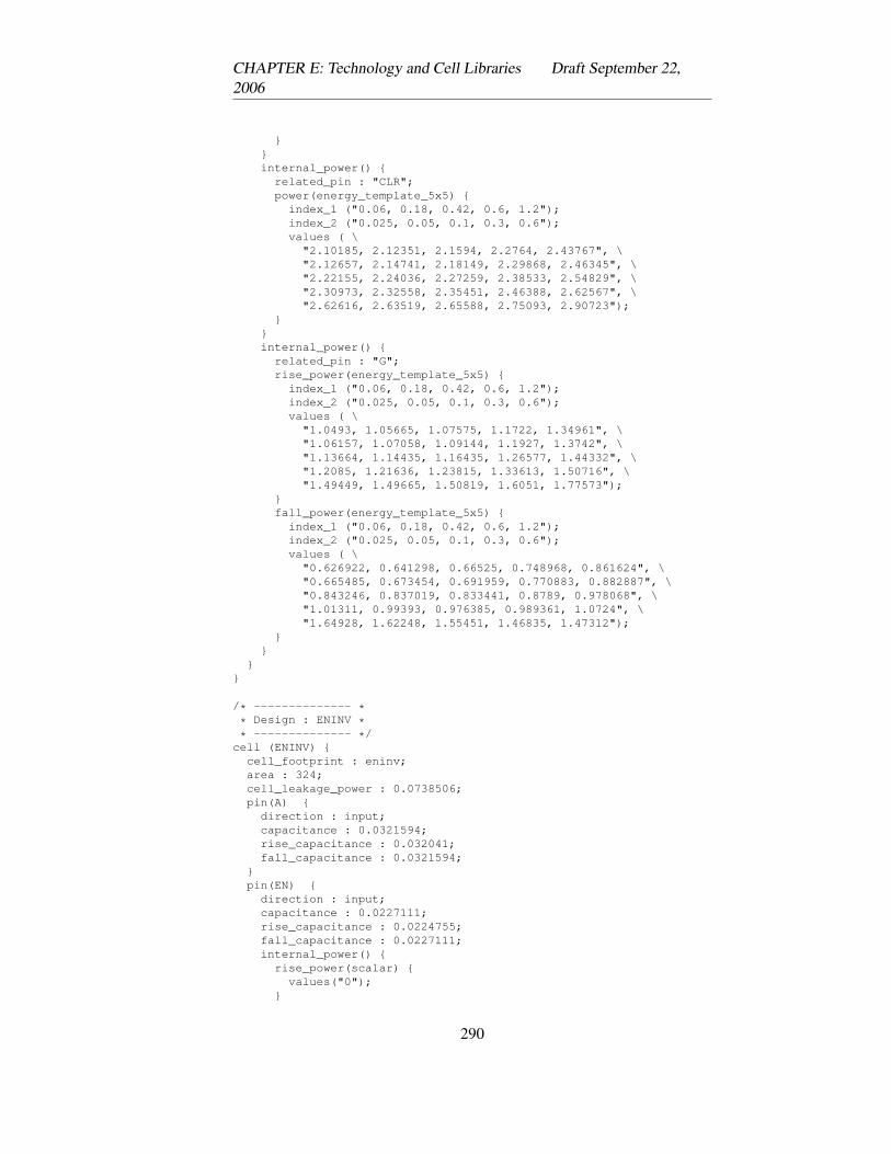
CHAPTER E: Technology and Cell Libraries Draft September 22,2006
}}internal_power() {
related_pin : "CLR";power(energy_template_5x5) {
index_1 ("0.06, 0.18, 0.42, 0.6, 1.2");index_2 ("0.025, 0.05, 0.1, 0.3, 0.6");values ( \
"2.10185, 2.12351, 2.1594, 2.2764, 2.43767", \"2.12657, 2.14741, 2.18149, 2.29868, 2.46345", \"2.22155, 2.24036, 2.27259, 2.38533, 2.54829", \"2.30973, 2.32558, 2.35451, 2.46388, 2.62567", \"2.62616, 2.63519, 2.65588, 2.75093, 2.90723");
}}internal_power() {
related_pin : "G";rise_power(energy_template_5x5) {
index_1 ("0.06, 0.18, 0.42, 0.6, 1.2");index_2 ("0.025, 0.05, 0.1, 0.3, 0.6");values ( \
"1.0493, 1.05665, 1.07575, 1.1722, 1.34961", \"1.06157, 1.07058, 1.09144, 1.1927, 1.3742", \"1.13664, 1.14435, 1.16435, 1.26577, 1.44332", \"1.2085, 1.21636, 1.23815, 1.33613, 1.50716", \"1.49449, 1.49665, 1.50819, 1.6051, 1.77573");
}fall_power(energy_template_5x5) {
index_1 ("0.06, 0.18, 0.42, 0.6, 1.2");index_2 ("0.025, 0.05, 0.1, 0.3, 0.6");values ( \
"0.626922, 0.641298, 0.66525, 0.748968, 0.861624", \"0.665485, 0.673454, 0.691959, 0.770883, 0.882887", \"0.843246, 0.837019, 0.833441, 0.8789, 0.978068", \"1.01311, 0.99393, 0.976385, 0.989361, 1.0724", \"1.64928, 1.62248, 1.55451, 1.46835, 1.47312");
}}
}}
/* -------------- ** Design : ENINV ** -------------- */
cell (ENINV) {cell_footprint : eninv;area : 324;cell_leakage_power : 0.0738506;pin(A) {
direction : input;capacitance : 0.0321594;rise_capacitance : 0.032041;fall_capacitance : 0.0321594;
}pin(EN) {
direction : input;capacitance : 0.0227111;rise_capacitance : 0.0224755;fall_capacitance : 0.0227111;internal_power() {
rise_power(scalar) {values("0");
}
290
Draft September 22, 2006 E.2: Standard Cell Libraries
fall_power(passive_energy_template_5x1) {index_1 ("0.06, 0.18, 0.42, 0.6, 1.2");values ("0.471294, 0.541237, 0.735163, 0.890906, 1.43609");
}}
}pin(Y) {
direction : output;capacitance : 0.019643;rise_capacitance : 0.019643;fall_capacitance : 0.0195901;max_capacitance : 0.456534;function : "(!A)";three_state : "(!EN)";timing() {
related_pin : "A";timing_sense : negative_unate;cell_rise(delay_template_5x5) {
index_1 ("0.06, 0.18, 0.42, 0.6, 1.2");index_2 ("0.044643, 0.069643, 0.119643, 0.319643, 0.619643");values ( \
"0.231543, 0.295486, 0.420722, 0.920277, 1.65986", \"0.281866, 0.344312, 0.469158, 0.961652, 1.70523", \"0.408865, 0.469576, 0.586993, 1.07167, 1.8032", \"0.507155, 0.568392, 0.687317, 1.15748, 1.89027", \"0.821945, 0.893387, 1.02316, 1.48403, 2.19312");
}rise_transition(delay_template_5x5) {
index_1 ("0.06, 0.18, 0.42, 0.6, 1.2");index_2 ("0.044643, 0.069643, 0.119643, 0.319643, 0.619643");values ( \
"0.157613, 0.218934, 0.343089, 0.831042, 1.56989", \"0.167199, 0.224339, 0.343477, 0.834151, 1.57532", \"0.225645, 0.272043, 0.373425, 0.836156, 1.56981", \"0.276151, 0.320372, 0.410994, 0.849582, 1.56901", \"0.446965, 0.491146, 0.569087, 0.941312, 1.60102");
}cell_fall(delay_template_5x5) {
index_1 ("0.06, 0.18, 0.42, 0.6, 1.2");index_2 ("0.0445901, 0.0695901, 0.11959, 0.31959, 0.61959");values ( \
"0.211275, 0.26897, 0.381301, 0.823526, 1.48457", \"0.256114, 0.311952, 0.423985, 0.864339, 1.52097", \"0.363252, 0.419315, 0.525177, 0.957198, 1.60822", \"0.442369, 0.499252, 0.606801, 1.02993, 1.67772", \"0.684617, 0.755665, 0.876926, 1.30314, 1.92799");
}fall_transition(delay_template_5x5) {
index_1 ("0.06, 0.18, 0.42, 0.6, 1.2");index_2 ("0.0445901, 0.0695901, 0.11959, 0.31959, 0.61959");values ( \
"0.150886, 0.203677, 0.30787, 0.731287, 1.36732", \"0.161691, 0.208762, 0.310394, 0.728784, 1.36267", \"0.219949, 0.258752, 0.34209, 0.734512, 1.35996", \"0.273229, 0.307864, 0.383115, 0.748592, 1.3634", \"0.440057, 0.482434, 0.549949, 0.851726, 1.41879");
}}timing() {
related_pin : "EN";timing_sense : positive_unate;timing_type : three_state_enable;cell_rise(delay_template_5x5) {
291
CHAPTER E: Technology and Cell Libraries Draft September 22,2006
index_1 ("0.06, 0.18, 0.42, 0.6, 1.2");index_2 ("0.044643, 0.069643, 0.119643, 0.319643, 0.619643");values ( \
"0.284987, 0.348123, 0.473392, 0.967588, 1.70718", \"0.382419, 0.445347, 0.569797, 1.06615, 1.80438", \"0.563654, 0.627346, 0.753711, 1.25257, 1.98628", \"0.693423, 0.758915, 0.881092, 1.37666, 2.12748", \"1.09888, 1.17084, 1.3014, 1.79342, 2.541");
}rise_transition(delay_template_5x5) {
index_1 ("0.06, 0.18, 0.42, 0.6, 1.2");index_2 ("0.044643, 0.069643, 0.119643, 0.319643, 0.619643");values ( \
"0.168633, 0.223147, 0.34324, 0.83535, 1.57157", \"0.170977, 0.226199, 0.343377, 0.833219, 1.5721", \"0.17112, 0.224139, 0.343229, 0.837152, 1.57167", \"0.179368, 0.228924, 0.341145, 0.829693, 1.57792", \"0.208461, 0.250794, 0.35033, 0.82941, 1.56762");
}cell_fall(delay_template_5x5) {
index_1 ("0.06, 0.18, 0.42, 0.6, 1.2");index_2 ("0.0445901, 0.0695901, 0.11959, 0.31959, 0.61959");values ( \
"0.15178, 0.209751, 0.321014, 0.764236, 1.42682", \"0.237819, 0.300427, 0.411592, 0.85449, 1.51687", \"0.36342, 0.450526, 0.58801, 1.03656, 1.70204", \"0.44242, 0.539813, 0.701024, 1.17134, 1.83043", \"0.651706, 0.788663, 1.00713, 1.60568, 2.2819");
}fall_transition(delay_template_5x5) {
index_1 ("0.06, 0.18, 0.42, 0.6, 1.2");index_2 ("0.0445901, 0.0695901, 0.11959, 0.31959, 0.61959");values ( \
"0.104133, 0.160605, 0.273405, 0.723412, 1.36831", \"0.132399, 0.181313, 0.278989, 0.720856, 1.37113", \"0.181987, 0.24516, 0.336736, 0.728872, 1.36169", \"0.217033, 0.279682, 0.384932, 0.756418, 1.36662", \"0.313155, 0.392265, 0.517552, 0.901574, 1.45979");
}}timing() {
related_pin : "EN";timing_sense : negative_unate;timing_type : three_state_disable;cell_rise(delay_template_5x1) {
index_1 ("0.06, 0.18, 0.42, 0.6, 1.2");values ("0.105616, 0.203647, 0.399709, 0.546756, 1.03691");
}rise_transition(scalar) {
values("0");}cell_fall(delay_template_5x1) {
index_1 ("0.06, 0.18, 0.42, 0.6, 1.2");values ("0.098026, 0.064018, 0.0, 0.0, 0.0");
}fall_transition(scalar) {
values("0");}
}internal_power() {
related_pin : "A";rise_power(energy_template_5x5) {
index_1 ("0.06, 0.18, 0.42, 0.6, 1.2");
292
Draft September 22, 2006 E.2: Standard Cell Libraries
index_2 ("0.044643, 0.069643, 0.119643, 0.319643, 0.619643");values ( \
"1.37914, 1.38369, 1.38815, 1.39306, 1.39471", \"1.41575, 1.40978, 1.40504, 1.39966, 1.3975", \"1.72818, 1.68171, 1.61946, 1.52492, 1.47776", \"2.03178, 1.96173, 1.86261, 1.67902, 1.58", \"3.15953, 3.04275, 2.8551, 2.42476, 2.13431");
}fall_power(energy_template_5x5) {
index_1 ("0.06, 0.18, 0.42, 0.6, 1.2");index_2 ("0.0445901, 0.0695901, 0.11959, 0.31959, 0.61959");values ( \
"0.064026, 0.067784, 0.071784, 0.076383, 0.077986", \"0.113509, 0.104997, 0.095238, 0.08408, 0.079851", \"0.408751, 0.362529, 0.301363, 0.191876, 0.155377", \"0.689885, 0.616902, 0.513429, 0.341686, 0.231254", \"1.77006, 1.64322, 1.446, 1.01412, 0.703659");
}}internal_power() {
related_pin : "EN";rise_power(energy_template_5x5) {
index_1 ("0.06, 0.18, 0.42, 0.6, 1.2");index_2 ("0.044643, 0.069643, 0.119643, 0.319643, 0.619643");values ( \
"1.12356, 1.12407, 1.12452, 1.12392, 1.12357", \"1.17161, 1.17088, 1.17163, 1.1721, 1.17217", \"1.33784, 1.34069, 1.34135, 1.34132, 1.34008", \"1.48843, 1.48639, 1.48704, 1.48461, 1.48334", \"2.00398, 2.00749, 2.01096, 2.01075, 2.00803");
}fall_power(energy_template_5x5) {
index_1 ("0.06, 0.18, 0.42, 0.6, 1.2");index_2 ("0.0445901, 0.0695901, 0.11959, 0.31959, 0.61959");values ( \
"0.419356, 0.41897, 0.418623, 0.418344, 0.418277", \"0.474271, 0.470872, 0.469518, 0.46768, 0.467427", \"0.664928, 0.655782, 0.65154, 0.645562, 0.643824", \"0.824271, 0.815601, 0.806621, 0.797667, 0.794933", \"1.38899, 1.37135, 1.35554, 1.33709, 1.3277");
}}
}}
/* -------------- ** Design : INVX1 ** -------------- */
cell (INVX1) {cell_footprint : inv;area : 129.6;cell_leakage_power : 0.0310651;pin(A) {
direction : input;capacitance : 0.0159685;rise_capacitance : 0.0159573;fall_capacitance : 0.0159685;
}pin(Y) {
direction : output;capacitance : 0;rise_capacitance : 0;fall_capacitance : 0;
293
CHAPTER E: Technology and Cell Libraries Draft September 22,2006
max_capacitance : 0.394734;function : "(!A)";timing() {
related_pin : "A";timing_sense : negative_unate;cell_rise(delay_template_5x5) {
index_1 ("0.06, 0.18, 0.42, 0.6, 1.2");index_2 ("0.025, 0.05, 0.1, 0.3, 0.6");values ( \
"0.147955, 0.218038, 0.359898, 0.922746, 1.76604", \"0.224384, 0.292903, 0.430394, 0.991288, 1.83116", \"0.365378, 0.448722, 0.584275, 1.13597, 1.97017", \"0.462096, 0.551586, 0.70164, 1.24437, 2.08131", \"0.756459, 0.874246, 1.05713, 1.62898, 2.44989");
}rise_transition(delay_template_5x5) {
index_1 ("0.06, 0.18, 0.42, 0.6, 1.2");index_2 ("0.025, 0.05, 0.1, 0.3, 0.6");values ( \
"0.097646, 0.166118, 0.305233, 0.855517, 1.68169", \"0.12087, 0.180331, 0.305311, 0.856547, 1.68363", \"0.175816, 0.236207, 0.344754, 0.854867, 1.67647", \"0.221599, 0.275198, 0.389989, 0.866611, 1.68061", \"0.327821, 0.409494, 0.526714, 0.97884, 1.71625");
}cell_fall(delay_template_5x5) {
index_1 ("0.06, 0.18, 0.42, 0.6, 1.2");index_2 ("0.025, 0.05, 0.1, 0.3, 0.6");values ( \
"0.168427, 0.249665, 0.41214, 1.06347, 2.02047", \"0.235098, 0.316001, 0.477491, 1.11802, 2.08758", \"0.366675, 0.457594, 0.614395, 1.25219, 2.22177", \"0.456999, 0.554239, 0.720463, 1.35319, 2.30488", \"0.732337, 0.85371, 1.05629, 1.70148, 2.65896");
}fall_transition(delay_template_5x5) {
index_1 ("0.06, 0.18, 0.42, 0.6, 1.2");index_2 ("0.025, 0.05, 0.1, 0.3, 0.6");values ( \
"0.104777, 0.181627, 0.32734, 0.929445, 1.79725", \"0.120705, 0.185144, 0.329039, 0.911419, 1.80491", \"0.180522, 0.242777, 0.364665, 0.924133, 1.82211", \"0.218513, 0.284372, 0.399704, 0.932018, 1.82289", \"0.338406, 0.422748, 0.54836, 1.02215, 1.84033");
}}internal_power() {
related_pin : "A";rise_power(energy_template_5x5) {
index_1 ("0.06, 0.18, 0.42, 0.6, 1.2");index_2 ("0.025, 0.05, 0.1, 0.3, 0.6");values ( \
"0.389884, 0.393267, 0.398283, 0.402712, 0.403947", \"0.442367, 0.433472, 0.422229, 0.416833, 0.409844", \"0.621677, 0.587412, 0.541775, 0.487576, 0.442274", \"0.765329, 0.724789, 0.653911, 0.549869, 0.513513", \"1.30339, 1.22138, 1.10368, 0.87106, 0.736151");
}fall_power(energy_template_5x5) {
index_1 ("0.06, 0.18, 0.42, 0.6, 1.2");index_2 ("0.025, 0.05, 0.1, 0.3, 0.6");values ( \
"0.012443, 0.004308, 0.000761, 0.005505, 0.006901", \
294
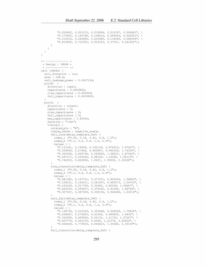
Draft September 22, 2006 E.2: Standard Cell Libraries
"0.026962, 0.021572, 0.019096, 0.012187, 0.008481", \"0.175583, 0.140788, 0.108614, 0.064456, 0.028351", \"0.315916, 0.264984, 0.203985, 0.118285, 0.086594", \"0.819665, 0.723352, 0.610353, 0.37551, 0.241641");
}}
}}
/* -------------- ** Design : INVX4 ** -------------- */
cell (INVX4) {cell_footprint : inv;area : 194.4;cell_leakage_power : 0.0627138;pin(A) {
direction : input;capacitance : 0.0659802;rise_capacitance : 0.065909;fall_capacitance : 0.0659802;
}pin(Y) {
direction : output;capacitance : 0;rise_capacitance : 0;fall_capacitance : 0;max_capacitance : 1.80656;function : "(!A)";timing() {
related_pin : "A";timing_sense : negative_unate;cell_rise(delay_template_5x5) {
index_1 ("0.06, 0.18, 0.42, 0.6, 1.2");index_2 ("0.1, 0.2, 0.4, 1.2, 2.4");values ( \
"0.131341, 0.19938, 0.332136, 0.870412, 1.67427", \"0.209954, 0.27454, 0.405897, 0.940326, 1.74355", \"0.350364, 0.429758, 0.560893, 1.08527, 1.87945", \"0.447117, 0.535454, 0.68169, 1.19366, 1.99119", \"0.746303, 0.863606, 1.0427, 1.59032, 2.36568");
}rise_transition(delay_template_5x5) {
index_1 ("0.06, 0.18, 0.42, 0.6, 1.2");index_2 ("0.1, 0.2, 0.4, 1.2, 2.4");values ( \
"0.081385, 0.147721, 0.277471, 0.802694, 1.58884", \"0.108531, 0.164311, 0.281697, 0.805573, 1.59703", \"0.163129, 0.217769, 0.32685, 0.80336, 1.58467", \"0.206105, 0.256657, 0.370492, 0.81546, 1.58706", \"0.307567, 0.387569, 0.508156, 0.944486, 1.63214");
}cell_fall(delay_template_5x5) {
index_1 ("0.06, 0.18, 0.42, 0.6, 1.2");index_2 ("0.1, 0.2, 0.4, 1.2, 2.4");values ( \
"0.138738, 0.210329, 0.353488, 0.928038, 1.79845", \"0.204947, 0.275855, 0.41693, 0.989893, 1.8432", \"0.324395, 0.409304, 0.55131, 1.11722, 1.97267", \"0.407779, 0.501274, 0.6569, 1.21374, 2.06522", \"0.658649, 0.779933, 0.969423, 1.55384, 2.39109");
}fall_transition(delay_template_5x5) {
295
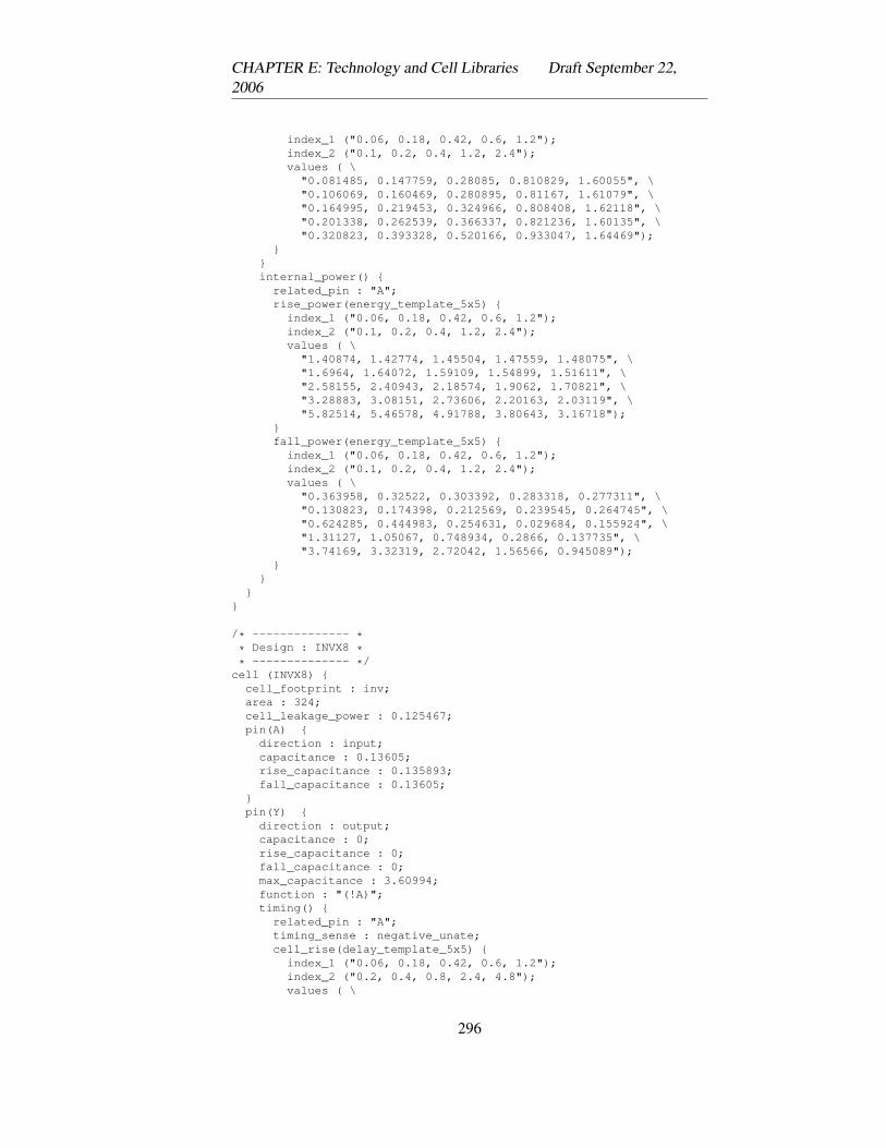
CHAPTER E: Technology and Cell Libraries Draft September 22,2006
index_1 ("0.06, 0.18, 0.42, 0.6, 1.2");index_2 ("0.1, 0.2, 0.4, 1.2, 2.4");values ( \
"0.081485, 0.147759, 0.28085, 0.810829, 1.60055", \"0.106069, 0.160469, 0.280895, 0.81167, 1.61079", \"0.164995, 0.219453, 0.324966, 0.808408, 1.62118", \"0.201338, 0.262539, 0.366337, 0.821236, 1.60135", \"0.320823, 0.393328, 0.520166, 0.933047, 1.64469");
}}internal_power() {
related_pin : "A";rise_power(energy_template_5x5) {
index_1 ("0.06, 0.18, 0.42, 0.6, 1.2");index_2 ("0.1, 0.2, 0.4, 1.2, 2.4");values ( \
"1.40874, 1.42774, 1.45504, 1.47559, 1.48075", \"1.6964, 1.64072, 1.59109, 1.54899, 1.51611", \"2.58155, 2.40943, 2.18574, 1.9062, 1.70821", \"3.28883, 3.08151, 2.73606, 2.20163, 2.03119", \"5.82514, 5.46578, 4.91788, 3.80643, 3.16718");
}fall_power(energy_template_5x5) {
index_1 ("0.06, 0.18, 0.42, 0.6, 1.2");index_2 ("0.1, 0.2, 0.4, 1.2, 2.4");values ( \
"0.363958, 0.32522, 0.303392, 0.283318, 0.277311", \"0.130823, 0.174398, 0.212569, 0.239545, 0.264745", \"0.624285, 0.444983, 0.254631, 0.029684, 0.155924", \"1.31127, 1.05067, 0.748934, 0.2866, 0.137735", \"3.74169, 3.32319, 2.72042, 1.56566, 0.945089");
}}
}}
/* -------------- ** Design : INVX8 ** -------------- */
cell (INVX8) {cell_footprint : inv;area : 324;cell_leakage_power : 0.125467;pin(A) {
direction : input;capacitance : 0.13605;rise_capacitance : 0.135893;fall_capacitance : 0.13605;
}pin(Y) {
direction : output;capacitance : 0;rise_capacitance : 0;fall_capacitance : 0;max_capacitance : 3.60994;function : "(!A)";timing() {
related_pin : "A";timing_sense : negative_unate;cell_rise(delay_template_5x5) {
index_1 ("0.06, 0.18, 0.42, 0.6, 1.2");index_2 ("0.2, 0.4, 0.8, 2.4, 4.8");values ( \
296
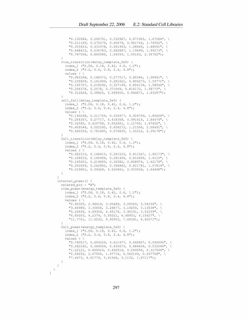
Draft September 22, 2006 E.2: Standard Cell Libraries
"0.132684, 0.200701, 0.332967, 0.871955, 1.67584", \"0.211169, 0.275276, 0.40676, 0.941744, 1.74502", \"0.353453, 0.431078, 0.561963, 1.08669, 1.88091", \"0.448415, 0.536783, 0.682887, 1.19499, 1.99273", \"0.747564, 0.865086, 1.04393, 1.59143, 2.36702");
}rise_transition(delay_template_5x5) {
index_1 ("0.06, 0.18, 0.42, 0.6, 1.2");index_2 ("0.2, 0.4, 0.8, 2.4, 4.8");values ( \
"0.082268, 0.148373, 0.277517, 0.80346, 1.58961", \"0.109409, 0.161494, 0.281621, 0.806273, 1.59771", \"0.165707, 0.218092, 0.327199, 0.804136, 1.58544", \"0.206378, 0.2578, 0.371069, 0.816172, 1.58775", \"0.312424, 0.38825, 0.508455, 0.944871, 1.63287");
}cell_fall(delay_template_5x5) {
index_1 ("0.06, 0.18, 0.42, 0.6, 1.2");index_2 ("0.2, 0.4, 0.8, 2.4, 4.8");values ( \
"0.140268, 0.211759, 0.354977, 0.929799, 1.80009", \"0.206357, 0.27717, 0.418358, 0.991414, 1.84474", \"0.32585, 0.410708, 0.552601, 1.11765, 1.97402", \"0.409344, 0.502595, 0.658272, 1.21506, 2.06491", \"0.660356, 0.781495, 0.970835, 1.55512, 2.39178");
}fall_transition(delay_template_5x5) {
index_1 ("0.06, 0.18, 0.42, 0.6, 1.2");index_2 ("0.2, 0.4, 0.8, 2.4, 4.8");values ( \
"0.082315, 0.148415, 0.281533, 0.811567, 1.60173", \"0.106633, 0.160964, 0.281456, 0.812406, 1.6115", \"0.165601, 0.219855, 0.32582, 0.808974, 1.62178", \"0.202059, 0.262802, 0.366882, 0.821781, 1.57819", \"0.319801, 0.39428, 0.520661, 0.933934, 1.64498");
}}internal_power() {
related_pin : "A";rise_power(energy_template_5x5) {
index_1 ("0.06, 0.18, 0.42, 0.6, 1.2");index_2 ("0.2, 0.4, 0.8, 2.4, 4.8");values ( \
"2.90305, 2.94614, 3.00489, 3.05069, 3.06236", \"3.46989, 3.35658, 3.26877, 3.19259, 3.13038", \"5.24405, 4.89304, 4.45174, 3.90191, 3.51039", \"6.65003, 6.2379, 5.55021, 4.48953, 4.15427", \"11.7761, 11.0032, 9.90953, 7.69391, 6.42071");
}fall_power(energy_template_5x5) {
index_1 ("0.06, 0.18, 0.42, 0.6, 1.2");index_2 ("0.2, 0.4, 0.8, 2.4, 4.8");values ( \
"0.740517, 0.659229, 0.611977, 0.568407, 0.555606", \"0.282242, 0.364504, 0.435673, 0.484434, 0.532046", \"1.22121, 0.869414, 0.492514, 0.049558, 0.317566", \"2.59252, 2.07505, 1.47718, 0.562149, 0.267708", \"7.4473, 6.61779, 5.41546, 3.1132, 1.87117");
}}
}}
297
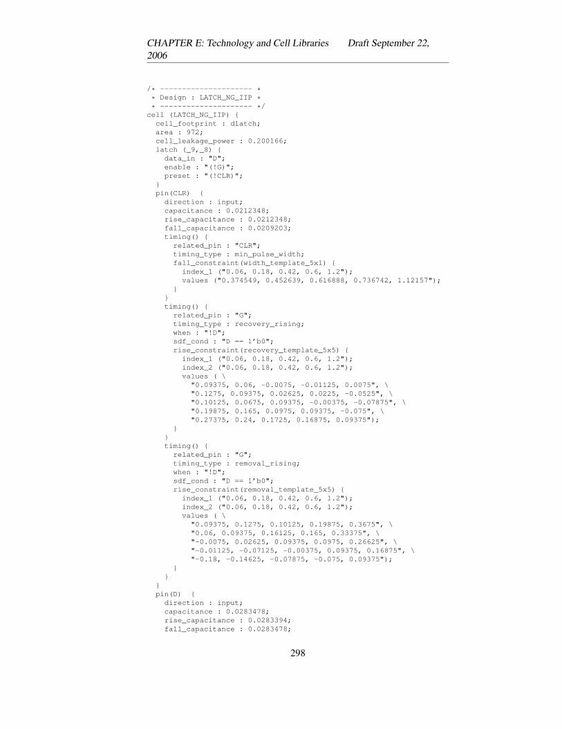
CHAPTER E: Technology and Cell Libraries Draft September 22,2006
/* --------------------- ** Design : LATCH_NG_IIP ** --------------------- */
cell (LATCH_NG_IIP) {cell_footprint : dlatch;area : 972;cell_leakage_power : 0.200166;latch (_9,_8) {
data_in : "D";enable : "(!G)";preset : "(!CLR)";
}pin(CLR) {
direction : input;capacitance : 0.0212348;rise_capacitance : 0.0212348;fall_capacitance : 0.0209203;timing() {
related_pin : "CLR";timing_type : min_pulse_width;fall_constraint(width_template_5x1) {
index_1 ("0.06, 0.18, 0.42, 0.6, 1.2");values ("0.374549, 0.452639, 0.616888, 0.736742, 1.12157");
}}timing() {
related_pin : "G";timing_type : recovery_rising;when : "!D";sdf_cond : "D == 1’b0";rise_constraint(recovery_template_5x5) {
index_1 ("0.06, 0.18, 0.42, 0.6, 1.2");index_2 ("0.06, 0.18, 0.42, 0.6, 1.2");values ( \
"0.09375, 0.06, -0.0075, -0.01125, 0.0075", \"0.1275, 0.09375, 0.02625, 0.0225, -0.0525", \"0.10125, 0.0675, 0.09375, -0.00375, -0.07875", \"0.19875, 0.165, 0.0975, 0.09375, -0.075", \"0.27375, 0.24, 0.1725, 0.16875, 0.09375");
}}timing() {
related_pin : "G";timing_type : removal_rising;when : "!D";sdf_cond : "D == 1’b0";rise_constraint(removal_template_5x5) {
index_1 ("0.06, 0.18, 0.42, 0.6, 1.2");index_2 ("0.06, 0.18, 0.42, 0.6, 1.2");values ( \
"0.09375, 0.1275, 0.10125, 0.19875, 0.3675", \"0.06, 0.09375, 0.16125, 0.165, 0.33375", \"-0.0075, 0.02625, 0.09375, 0.0975, 0.26625", \"-0.01125, -0.07125, -0.00375, 0.09375, 0.16875", \"-0.18, -0.14625, -0.07875, -0.075, 0.09375");
}}
}pin(D) {
direction : input;capacitance : 0.0283478;rise_capacitance : 0.0283394;fall_capacitance : 0.0283478;
298
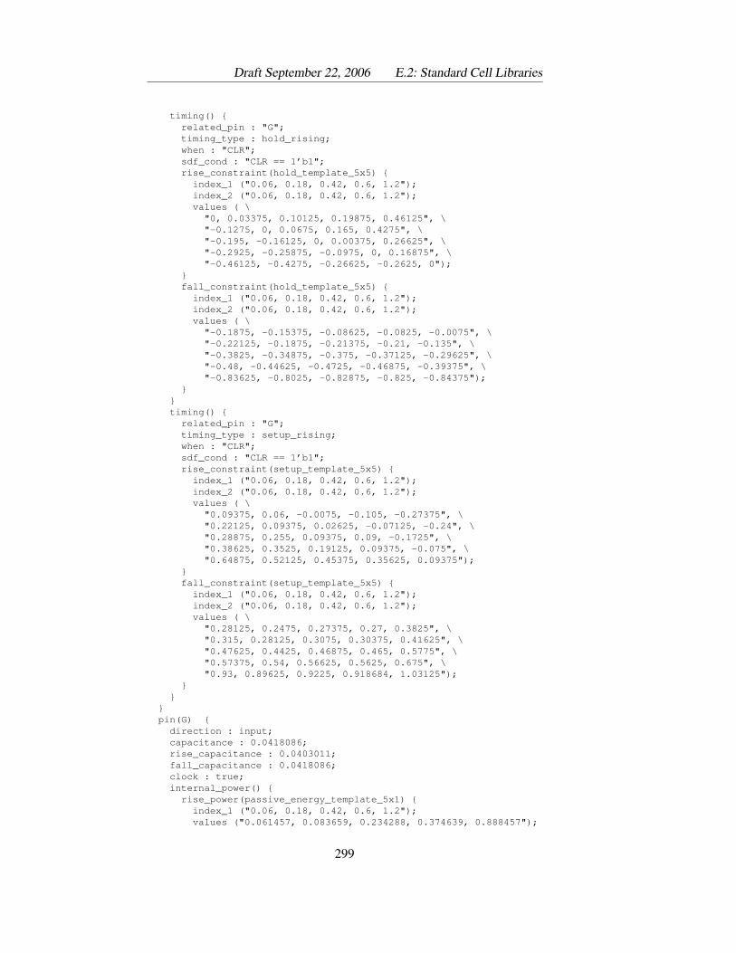
Draft September 22, 2006 E.2: Standard Cell Libraries
timing() {related_pin : "G";timing_type : hold_rising;when : "CLR";sdf_cond : "CLR == 1’b1";rise_constraint(hold_template_5x5) {
index_1 ("0.06, 0.18, 0.42, 0.6, 1.2");index_2 ("0.06, 0.18, 0.42, 0.6, 1.2");values ( \
"0, 0.03375, 0.10125, 0.19875, 0.46125", \"-0.1275, 0, 0.0675, 0.165, 0.4275", \"-0.195, -0.16125, 0, 0.00375, 0.26625", \"-0.2925, -0.25875, -0.0975, 0, 0.16875", \"-0.46125, -0.4275, -0.26625, -0.2625, 0");
}fall_constraint(hold_template_5x5) {
index_1 ("0.06, 0.18, 0.42, 0.6, 1.2");index_2 ("0.06, 0.18, 0.42, 0.6, 1.2");values ( \
"-0.1875, -0.15375, -0.08625, -0.0825, -0.0075", \"-0.22125, -0.1875, -0.21375, -0.21, -0.135", \"-0.3825, -0.34875, -0.375, -0.37125, -0.29625", \"-0.48, -0.44625, -0.4725, -0.46875, -0.39375", \"-0.83625, -0.8025, -0.82875, -0.825, -0.84375");
}}timing() {
related_pin : "G";timing_type : setup_rising;when : "CLR";sdf_cond : "CLR == 1’b1";rise_constraint(setup_template_5x5) {
index_1 ("0.06, 0.18, 0.42, 0.6, 1.2");index_2 ("0.06, 0.18, 0.42, 0.6, 1.2");values ( \
"0.09375, 0.06, -0.0075, -0.105, -0.27375", \"0.22125, 0.09375, 0.02625, -0.07125, -0.24", \"0.28875, 0.255, 0.09375, 0.09, -0.1725", \"0.38625, 0.3525, 0.19125, 0.09375, -0.075", \"0.64875, 0.52125, 0.45375, 0.35625, 0.09375");
}fall_constraint(setup_template_5x5) {
index_1 ("0.06, 0.18, 0.42, 0.6, 1.2");index_2 ("0.06, 0.18, 0.42, 0.6, 1.2");values ( \
"0.28125, 0.2475, 0.27375, 0.27, 0.3825", \"0.315, 0.28125, 0.3075, 0.30375, 0.41625", \"0.47625, 0.4425, 0.46875, 0.465, 0.5775", \"0.57375, 0.54, 0.56625, 0.5625, 0.675", \"0.93, 0.89625, 0.9225, 0.918684, 1.03125");
}}
}pin(G) {
direction : input;capacitance : 0.0418086;rise_capacitance : 0.0403011;fall_capacitance : 0.0418086;clock : true;internal_power() {
rise_power(passive_energy_template_5x1) {index_1 ("0.06, 0.18, 0.42, 0.6, 1.2");values ("0.061457, 0.083659, 0.234288, 0.374639, 0.888457");
299
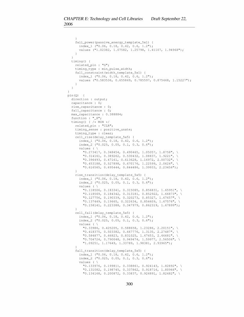
CHAPTER E: Technology and Cell Libraries Draft September 22,2006
}fall_power(passive_energy_template_5x1) {
index_1 ("0.06, 0.18, 0.42, 0.6, 1.2");values ("1.02382, 1.07582, 1.25798, 1.41107, 1.94968");
}}timing() {
related_pin : "G";timing_type : min_pulse_width;fall_constraint(width_template_5x1) {
index_1 ("0.06, 0.18, 0.42, 0.6, 1.2");values ("0.583536, 0.655849, 0.785597, 0.875448, 1.15227");
}}
}pin(Q) {
direction : output;capacitance : 0;rise_capacitance : 0;fall_capacitance : 0;max_capacitance : 0.388884;function : "_8";timing() { /* MIN */
related_pin : "CLR";timing_sense : positive_unate;timing_type : clear;cell_rise(delay_template_5x5) {
index_1 ("0.06, 0.18, 0.42, 0.6, 1.2");index_2 ("0.025, 0.05, 0.1, 0.3, 0.6");values ( \
"0.273417, 0.348454, 0.490465, 1.05057, 1.8758", \"0.314161, 0.389262, 0.530432, 1.08837, 1.9221", \"0.396493, 0.47161, 0.613628, 1.16972, 2.00732", \"0.453188, 0.527898, 0.670176, 1.22599, 2.0624", \"0.616565, 0.695444, 0.844486, 1.39933, 2.23456");
}rise_transition(delay_template_5x5) {
index_1 ("0.06, 0.18, 0.42, 0.6, 1.2");index_2 ("0.025, 0.05, 0.1, 0.3, 0.6");values ( \
"0.118506, 0.183341, 0.315085, 0.856831, 1.65951", \"0.118569, 0.184342, 0.313181, 0.852922, 1.66873", \"0.127756, 0.190339, 0.320273, 0.85327, 1.67657", \"0.137449, 0.19665, 0.322634, 0.854609, 1.67576", \"0.158141, 0.223388, 0.347979, 0.862319, 1.67899");
}cell_fall(delay_template_5x5) {
index_1 ("0.06, 0.18, 0.42, 0.6, 1.2");index_2 ("0.025, 0.05, 0.1, 0.3, 0.6");values ( \
"0.33986, 0.425205, 0.588658, 1.23286, 2.20151", \"0.418375, 0.503382, 0.667776, 1.3135, 2.27487", \"0.584877, 0.66823, 0.831025, 1.47453, 2.46681", \"0.704724, 0.790048, 0.949474, 1.59977, 2.56506", \"1.09251, 1.17649, 1.33789, 1.98381, 2.93965");
}fall_transition(delay_template_5x5) {
index_1 ("0.06, 0.18, 0.42, 0.6, 1.2");index_2 ("0.025, 0.05, 0.1, 0.3, 0.6");values ( \
"0.133976, 0.199811, 0.338861, 0.924143, 1.82892", \"0.131082, 0.198745, 0.337862, 0.918716, 1.80966", \"0.134168, 0.200872, 0.33837, 0.924891, 1.82482", \
300
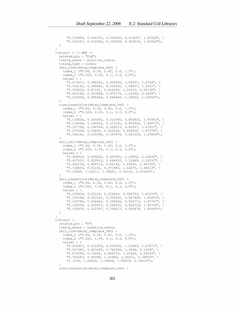
Draft September 22, 2006 E.2: Standard Cell Libraries
"0.139969, 0.204733, 0.340042, 0.916297, 1.81524", \"0.152547, 0.212024, 0.341858, 0.924019, 1.82042");
}}timing() { /* MAX */
related_pin : "CLR";timing_sense : positive_unate;timing_type : clear;cell_rise(delay_template_5x5) {
index_1 ("0.06, 0.18, 0.42, 0.6, 1.2");index_2 ("0.025, 0.05, 0.1, 0.3, 0.6");values ( \
"0.273417, 0.348454, 0.490465, 1.05057, 1.8758", \"0.314161, 0.389262, 0.530432, 1.08837, 1.9221", \"0.396493, 0.47161, 0.613628, 1.16972, 2.00732", \"0.453188, 0.527898, 0.670176, 1.22599, 2.0624", \"0.616565, 0.695444, 0.844486, 1.39933, 2.23456");
}rise_transition(delay_template_5x5) {
index_1 ("0.06, 0.18, 0.42, 0.6, 1.2");index_2 ("0.025, 0.05, 0.1, 0.3, 0.6");values ( \
"0.118506, 0.183341, 0.315085, 0.856831, 1.65951", \"0.118569, 0.184342, 0.313181, 0.852922, 1.66873", \"0.127756, 0.190339, 0.320273, 0.85327, 1.67657", \"0.137449, 0.19665, 0.322634, 0.854609, 1.67576", \"0.158141, 0.223388, 0.347979, 0.862319, 1.67899");
}cell_fall(delay_template_5x5) {
index_1 ("0.06, 0.18, 0.42, 0.6, 1.2");index_2 ("0.025, 0.05, 0.1, 0.3, 0.6");values ( \
"0.358818, 0.444252, 0.607591, 1.25802, 2.23432", \"0.437527, 0.522812, 0.684622, 1.33489, 2.30252", \"0.606156, 0.689715, 0.85142, 1.49691, 2.46705", \"0.728503, 0.81161, 0.971983, 1.62275, 2.58413", \"1.12089, 1.20211, 1.35851, 2.00161, 2.97042");
}fall_transition(delay_template_5x5) {
index_1 ("0.06, 0.18, 0.42, 0.6, 1.2");index_2 ("0.025, 0.05, 0.1, 0.3, 0.6");values ( \
"0.135429, 0.20118, 0.339429, 0.926763, 1.83159", \"0.135194, 0.201043, 0.338592, 0.927894, 1.82453", \"0.136784, 0.202446, 0.340432, 0.926773, 1.83767", \"0.140049, 0.205427, 0.340201, 0.922319, 1.82736", \"0.159676, 0.222397, 0.348013, 0.926878, 1.82592");
}}timing() {
related_pin : "D";timing_sense : negative_unate;cell_rise(delay_template_5x5) {
index_1 ("0.06, 0.18, 0.42, 0.6, 1.2");index_2 ("0.025, 0.05, 0.1, 0.3, 0.6");values ( \
"0.455907, 0.532329, 0.675205, 1.23583, 2.07071", \"0.527087, 0.603499, 0.746309, 1.3068, 2.1428", \"0.676566, 0.75258, 0.896475, 1.45429, 2.29224", \"0.783287, 0.85994, 1.00484, 1.56471, 2.38852", \"1.1278, 1.20429, 1.34896, 1.90879, 2.74433");
}rise_transition(delay_template_5x5) {
301
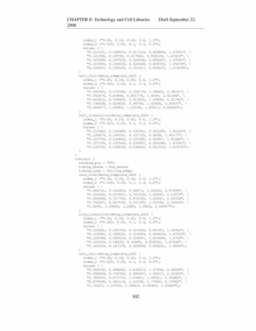
CHAPTER E: Technology and Cell Libraries Draft September 22,2006
index_1 ("0.06, 0.18, 0.42, 0.6, 1.2");index_2 ("0.025, 0.05, 0.1, 0.3, 0.6");values ( \
"0.121331, 0.188026, 0.317103, 0.858849, 1.67431", \"0.121358, 0.18799, 0.317643, 0.858188, 1.67609", \"0.121898, 0.187553, 0.320096, 0.854067, 1.67541", \"0.123093, 0.190039, 0.320668, 0.859703, 1.65678", \"0.124557, 0.190229, 0.321417, 0.858675, 1.67609");
}cell_fall(delay_template_5x5) {
index_1 ("0.06, 0.18, 0.42, 0.6, 1.2");index_2 ("0.025, 0.05, 0.1, 0.3, 0.6");values ( \
"0.491852, 0.576786, 0.740779, 1.38668, 2.36151", \"0.552674, 0.63848, 0.801778, 1.4549, 2.41144", \"0.663811, 0.749925, 0.913031, 1.56495, 2.51762", \"0.738428, 0.824825, 0.98759, 1.63445, 2.60637", \"0.964477, 1.04963, 1.21186, 1.85817, 2.82406");
}fall_transition(delay_template_5x5) {
index_1 ("0.06, 0.18, 0.42, 0.6, 1.2");index_2 ("0.025, 0.05, 0.1, 0.3, 0.6");values ( \
"0.127662, 0.195489, 0.335241, 0.925265, 1.81435", \"0.126479, 0.196591, 0.337725, 0.9299, 1.82177", \"0.127794, 0.196893, 0.337995, 0.92957, 1.81985", \"0.127165, 0.197546, 0.335857, 0.924286, 1.83341", \"0.130752, 0.199259, 0.338622, 0.921533, 1.81972");
}}timing() {
related_pin : "G";timing_sense : non_unate;timing_type : falling_edge;cell_rise(delay_template_5x5) {
index_1 ("0.06, 0.18, 0.42, 0.6, 1.2");index_2 ("0.025, 0.05, 0.1, 0.3, 0.6");values ( \
"0.466701, 0.542603, 0.68475, 1.24206, 2.07599", \"0.522652, 0.597857, 0.741039, 1.29491, 2.13574", \"0.653466, 0.727793, 0.872105, 1.42847, 2.26728", \"0.752207, 0.827535, 0.971765, 1.52596, 2.36559", \"1.0691, 1.14404, 1.2885, 1.8455, 2.66987");
}rise_transition(delay_template_5x5) {
index_1 ("0.06, 0.18, 0.42, 0.6, 1.2");index_2 ("0.025, 0.05, 0.1, 0.3, 0.6");values ( \
"0.119281, 0.185709, 0.315364, 0.85181, 1.66902", \"0.119382, 0.185535, 0.316904, 0.848633, 1.67529", \"0.120384, 0.185616, 0.318497, 0.853684, 1.6766", \"0.121039, 0.18639, 0.31885, 0.850052, 1.67448", \"0.123539, 0.187378, 0.320834, 0.855221, 1.6545");
}cell_fall(delay_template_5x5) {
index_1 ("0.06, 0.18, 0.42, 0.6, 1.2");index_2 ("0.025, 0.05, 0.1, 0.3, 0.6");values ( \
"0.583536, 0.668202, 0.833013, 1.47666, 2.46296", \"0.655849, 0.739764, 0.905497, 1.56017, 2.52455", \"0.785597, 0.870733, 1.03461, 1.68321, 2.65984", \"0.875448, 0.961116, 1.12339, 1.77645, 2.73982", \"1.15227, 1.23724, 1.39816, 2.04383, 3.02804");
302
Draft September 22, 2006 E.2: Standard Cell Libraries
}fall_transition(delay_template_5x5) {
index_1 ("0.06, 0.18, 0.42, 0.6, 1.2");index_2 ("0.025, 0.05, 0.1, 0.3, 0.6");values ( \
"0.126119, 0.19568, 0.335083, 0.925035, 1.82573", \"0.126179, 0.195428, 0.336692, 0.929011, 1.81796", \"0.12579, 0.195893, 0.334103, 0.922281, 1.82647", \"0.125564, 0.195723, 0.336301, 0.921131, 1.80943", \"0.125794, 0.19494, 0.334015, 0.923104, 1.82691");
}}internal_power() {
related_pin : "CLR";rise_power(energy_template_5x5) {
index_1 ("0.06, 0.18, 0.42, 0.6, 1.2");index_2 ("0.025, 0.05, 0.1, 0.3, 0.6");values ( \
"1.00349, 1.0034, 1.00415, 1.0049, 1.00508", \"1.06693, 1.06405, 1.06262, 1.06179, 1.06157", \"1.32981, 1.31812, 1.3084, 1.29894, 1.29566", \"1.56667, 1.54881, 1.5328, 1.51401, 1.50753", \"2.43013, 2.39513, 2.36113, 2.31544, 2.29539");
}fall_power(energy_template_5x5) {
index_1 ("0.06, 0.18, 0.42, 0.6, 1.2");index_2 ("0.025, 0.05, 0.1, 0.3, 0.6");values ( \
"1.64095, 1.63743, 1.63483, 1.63259, 1.63184", \"1.71412, 1.70898, 1.70351, 1.70073, 1.70015", \"1.9975, 1.98486, 1.97472, 1.96607, 1.96393", \"2.25291, 2.23548, 2.2191, 2.20292, 2.19834", \"3.16252, 3.12847, 3.09702, 3.05518, 3.04107");
}}internal_power() {
related_pin : "D";rise_power(energy_template_5x5) {
index_1 ("0.06, 0.18, 0.42, 0.6, 1.2");index_2 ("0.025, 0.05, 0.1, 0.3, 0.6");values ( \
"2.33251, 2.32931, 2.32756, 2.32596, 2.32523", \"2.38942, 2.38629, 2.38469, 2.38354, 2.38299", \"2.65151, 2.64779, 2.64594, 2.645, 2.64465", \"2.88678, 2.8828, 2.88022, 2.87943, 2.87957", \"3.75229, 3.74558, 3.74109, 3.73807, 3.73746");
}fall_power(energy_template_5x5) {
index_1 ("0.06, 0.18, 0.42, 0.6, 1.2");index_2 ("0.025, 0.05, 0.1, 0.3, 0.6");values ( \
"1.60466, 1.60391, 1.60421, 1.60402, 1.60366", \"1.648, 1.64706, 1.64739, 1.64759, 1.64723", \"1.85893, 1.85685, 1.85649, 1.85658, 1.85638", \"2.05772, 2.05524, 2.05475, 2.05511, 2.05513", \"2.83505, 2.83166, 2.82966, 2.82835, 2.8285");
}}internal_power() {
related_pin : "G";rise_power(energy_template_5x5) {
index_1 ("0.06, 0.18, 0.42, 0.6, 1.2");index_2 ("0.025, 0.05, 0.1, 0.3, 0.6");
303
CHAPTER E: Technology and Cell Libraries Draft September 22,2006
values ( \"3.16702, 3.1646, 3.16363, 3.16303, 3.16271", \"3.26187, 3.25961, 3.25911, 3.25919, 3.2591", \"3.76565, 3.76237, 3.76105, 3.76078, 3.76074", \"4.21797, 4.21365, 4.21151, 4.2109, 4.21085", \"5.79016, 5.78252, 5.77479, 5.77297, 5.77237");
}fall_power(energy_template_5x5) {
index_1 ("0.06, 0.18, 0.42, 0.6, 1.2");index_2 ("0.025, 0.05, 0.1, 0.3, 0.6");values ( \
"2.92547, 2.92643, 2.92682, 2.92754, 2.92754", \"2.98637, 2.98658, 2.98717, 2.98792, 2.98792", \"3.20538, 3.20584, 3.20701, 3.20786, 3.20781", \"3.39324, 3.39268, 3.39353, 3.3947, 3.3946", \"4.04803, 4.04889, 4.04983, 4.05054, 4.05062");
}}
}}
/* ----------------- ** Design : MUX2_INV ** ----------------- */
cell (MUX2_INV) {cell_footprint : mux2inv;area : 388.8;cell_leakage_power : 0.110151;pin(A) {
direction : input;capacitance : 0.0271855;rise_capacitance : 0.0271855;fall_capacitance : 0.0271766;
}pin(B) {
direction : input;capacitance : 0.027185;rise_capacitance : 0.027185;fall_capacitance : 0.02718;
}pin(S) {
direction : input;capacitance : 0.0410369;rise_capacitance : 0.0408778;fall_capacitance : 0.0410369;
}pin(Y) {
direction : output;capacitance : 0;rise_capacitance : 0;fall_capacitance : 0;max_capacitance : 0.322878;function : "(!((S B) + (!S A)))";timing() { /* MIN */
related_pin : "A";timing_sense : negative_unate;cell_rise(delay_template_5x5) {
index_1 ("0.06, 0.18, 0.42, 0.6, 1.2");index_2 ("0.025, 0.05, 0.1, 0.3, 0.6");values ( \
"0.259069, 0.345793, 0.516368, 1.1853, 2.18738", \"0.328795, 0.411994, 0.57966, 1.24846, 2.25934", \"0.490729, 0.570364, 0.732285, 1.38983, 2.38874", \
304
Draft September 22, 2006 E.2: Standard Cell Libraries
"0.603514, 0.693475, 0.851956, 1.50074, 2.49949", \"0.974876, 1.07342, 1.25327, 1.89583, 2.87432");
}rise_transition(delay_template_5x5) {
index_1 ("0.06, 0.18, 0.42, 0.6, 1.2");index_2 ("0.025, 0.05, 0.1, 0.3, 0.6");values ( \
"0.197837, 0.282679, 0.450545, 1.11442, 2.10901", \"0.202809, 0.281481, 0.446533, 1.11337, 2.11019", \"0.245392, 0.314126, 0.467505, 1.11366, 2.11437", \"0.280012, 0.348846, 0.497053, 1.1145, 2.10856", \"0.391718, 0.466303, 0.607547, 1.19708, 2.11645");
}cell_fall(delay_template_5x5) {
index_1 ("0.06, 0.18, 0.42, 0.6, 1.2");index_2 ("0.025, 0.05, 0.1, 0.3, 0.6");values ( \
"0.1749, 0.231154, 0.341566, 0.784728, 1.4455", \"0.237926, 0.292344, 0.402925, 0.842986, 1.4985", \"0.350166, 0.415041, 0.529846, 0.967314, 1.62016", \"0.423297, 0.49737, 0.621672, 1.06209, 1.71701", \"0.642071, 0.736151, 0.892615, 1.38391, 2.02785");
}fall_transition(delay_template_5x5) {
index_1 ("0.06, 0.18, 0.42, 0.6, 1.2");index_2 ("0.025, 0.05, 0.1, 0.3, 0.6");values ( \
"0.121781, 0.175615, 0.28129, 0.703688, 1.33825", \"0.141418, 0.185879, 0.283409, 0.704088, 1.33598", \"0.202735, 0.248829, 0.331713, 0.708558, 1.33704", \"0.240927, 0.296251, 0.380932, 0.731634, 1.33941", \"0.384635, 0.438224, 0.532089, 0.873041, 1.40308");
}}timing() { /* MAX */
related_pin : "A";timing_sense : negative_unate;cell_rise(delay_template_5x5) {
index_1 ("0.06, 0.18, 0.42, 0.6, 1.2");index_2 ("0.025, 0.05, 0.1, 0.3, 0.6");values ( \
"0.260421, 0.346738, 0.517384, 1.19059, 2.18967", \"0.333235, 0.414988, 0.582769, 1.25466, 2.261", \"0.496326, 0.576241, 0.73557, 1.39826, 2.39965", \"0.612516, 0.698512, 0.857392, 1.51118, 2.50422", \"0.989332, 1.08559, 1.25871, 1.90339, 2.875");
}rise_transition(delay_template_5x5) {
index_1 ("0.06, 0.18, 0.42, 0.6, 1.2");index_2 ("0.025, 0.05, 0.1, 0.3, 0.6");values ( \
"0.224147, 0.308646, 0.475434, 1.13944, 2.13636", \"0.2361, 0.311391, 0.472546, 1.13899, 2.135", \"0.283101, 0.34685, 0.497724, 1.14446, 2.14539", \"0.322699, 0.385663, 0.521896, 1.14904, 2.14568", \"0.446047, 0.51228, 0.644925, 1.22246, 2.15303");
}cell_fall(delay_template_5x5) {
index_1 ("0.06, 0.18, 0.42, 0.6, 1.2");index_2 ("0.025, 0.05, 0.1, 0.3, 0.6");values ( \
"0.195823, 0.253362, 0.366402, 0.806399, 1.46913", \"0.257873, 0.313274, 0.424917, 0.866772, 1.52476", \
305
CHAPTER E: Technology and Cell Libraries Draft September 22,2006
"0.374352, 0.439652, 0.551996, 0.988397, 1.64348", \"0.450018, 0.520031, 0.648961, 1.0834, 1.73739", \"0.671674, 0.76256, 0.918492, 1.41262, 2.05612");
}fall_transition(delay_template_5x5) {
index_1 ("0.06, 0.18, 0.42, 0.6, 1.2");index_2 ("0.025, 0.05, 0.1, 0.3, 0.6");values ( \
"0.131293, 0.185025, 0.291607, 0.714501, 1.35143", \"0.143425, 0.191041, 0.291743, 0.715865, 1.34905", \"0.20657, 0.253159, 0.336192, 0.718537, 1.34969", \"0.258825, 0.297599, 0.384853, 0.73767, 1.34982", \"0.399492, 0.452253, 0.544224, 0.885365, 1.41008");
}}timing() { /* MIN */
related_pin : "B";timing_sense : negative_unate;cell_rise(delay_template_5x5) {
index_1 ("0.06, 0.18, 0.42, 0.6, 1.2");index_2 ("0.025, 0.05, 0.1, 0.3, 0.6");values ( \
"0.258461, 0.345104, 0.514685, 1.18574, 2.19029", \"0.328516, 0.411042, 0.58001, 1.24766, 2.2505", \"0.490566, 0.57017, 0.732149, 1.3975, 2.38686", \"0.603431, 0.693311, 0.852267, 1.5007, 2.49413", \"0.974803, 1.07339, 1.25238, 1.89319, 2.86523");
}rise_transition(delay_template_5x5) {
index_1 ("0.06, 0.18, 0.42, 0.6, 1.2");index_2 ("0.025, 0.05, 0.1, 0.3, 0.6");values ( \
"0.197898, 0.281806, 0.446523, 1.11283, 2.10793", \"0.202805, 0.281113, 0.448033, 1.1141, 2.11764", \"0.245874, 0.312579, 0.468265, 1.11677, 2.11107", \"0.280988, 0.350819, 0.496963, 1.11515, 2.11169", \"0.391383, 0.466951, 0.614344, 1.18775, 2.12259");
}cell_fall(delay_template_5x5) {
index_1 ("0.06, 0.18, 0.42, 0.6, 1.2");index_2 ("0.025, 0.05, 0.1, 0.3, 0.6");values ( \
"0.174878, 0.231335, 0.34278, 0.782917, 1.44249", \"0.237903, 0.292639, 0.401931, 0.84204, 1.50006", \"0.349198, 0.415503, 0.529856, 0.964353, 1.61842", \"0.423358, 0.496216, 0.622816, 1.06255, 1.71748", \"0.641903, 0.734599, 0.893908, 1.38355, 2.03142");
}fall_transition(delay_template_5x5) {
index_1 ("0.06, 0.18, 0.42, 0.6, 1.2");index_2 ("0.025, 0.05, 0.1, 0.3, 0.6");values ( \
"0.122649, 0.175352, 0.280059, 0.704137, 1.33486", \"0.142425, 0.185441, 0.284785, 0.703066, 1.3364", \"0.201416, 0.249441, 0.332969, 0.710203, 1.33711", \"0.2423, 0.294442, 0.381309, 0.730054, 1.33926", \"0.384459, 0.43801, 0.531761, 0.872817, 1.40087");
}}timing() { /* MAX */
related_pin : "B";timing_sense : negative_unate;cell_rise(delay_template_5x5) {
306
Draft September 22, 2006 E.2: Standard Cell Libraries
index_1 ("0.06, 0.18, 0.42, 0.6, 1.2");index_2 ("0.025, 0.05, 0.1, 0.3, 0.6");values ( \
"0.25996, 0.346456, 0.516488, 1.18749, 2.19434", \"0.33297, 0.414734, 0.58122, 1.25082, 2.25316", \"0.496149, 0.57503, 0.735423, 1.39804, 2.39628", \"0.612438, 0.698176, 0.857514, 1.51041, 2.50691", \"0.989357, 1.08556, 1.26025, 1.90053, 2.87681");
}rise_transition(delay_template_5x5) {
index_1 ("0.06, 0.18, 0.42, 0.6, 1.2");index_2 ("0.025, 0.05, 0.1, 0.3, 0.6");values ( \
"0.225063, 0.308318, 0.473132, 1.13402, 2.14449", \"0.235722, 0.311307, 0.475099, 1.13381, 2.12877", \"0.281825, 0.34942, 0.498306, 1.14409, 2.14608", \"0.322375, 0.386225, 0.521254, 1.14893, 2.14767", \"0.445873, 0.513085, 0.650096, 1.22717, 2.1634");
}cell_fall(delay_template_5x5) {
index_1 ("0.06, 0.18, 0.42, 0.6, 1.2");index_2 ("0.025, 0.05, 0.1, 0.3, 0.6");values ( \
"0.19595, 0.253095, 0.366366, 0.813457, 1.47113", \"0.258025, 0.313117, 0.42471, 0.866519, 1.52724", \"0.374035, 0.441974, 0.552981, 0.987758, 1.64999", \"0.44979, 0.520199, 0.64891, 1.08485, 1.73808", \"0.671706, 0.762533, 0.918419, 1.41244, 2.05386");
}fall_transition(delay_template_5x5) {
index_1 ("0.06, 0.18, 0.42, 0.6, 1.2");index_2 ("0.025, 0.05, 0.1, 0.3, 0.6");values ( \
"0.130985, 0.184291, 0.291209, 0.717763, 1.35614", \"0.142837, 0.191139, 0.291479, 0.714196, 1.35133", \"0.209094, 0.254028, 0.335857, 0.7185, 1.35148", \"0.253986, 0.297669, 0.384169, 0.734032, 1.34925", \"0.399442, 0.449783, 0.543844, 0.884942, 1.41103");
}}timing() {
related_pin : "S";timing_sense : positive_unate;cell_rise(delay_template_5x5) {
index_1 ("0.06, 0.18, 0.42, 0.6, 1.2");index_2 ("0.025, 0.05, 0.1, 0.3, 0.6");values ( \
"0.390901, 0.474931, 0.643362, 1.31298, 2.32505", \"0.458415, 0.541577, 0.710983, 1.38297, 2.3817", \"0.583736, 0.666397, 0.83614, 1.50893, 2.50744", \"0.672003, 0.753463, 0.920083, 1.58537, 2.6028", \"0.946137, 1.02571, 1.18804, 1.84531, 2.85912");
}rise_transition(delay_template_5x5) {
index_1 ("0.06, 0.18, 0.42, 0.6, 1.2");index_2 ("0.025, 0.05, 0.1, 0.3, 0.6");values ( \
"0.201697, 0.282069, 0.447506, 1.11474, 2.10569", \"0.20325, 0.282591, 0.449065, 1.111, 2.10746", \"0.20636, 0.285504, 0.451092, 1.11743, 2.10751", \"0.208748, 0.28832, 0.450726, 1.11355, 2.11884", \"0.224138, 0.297885, 0.455137, 1.11244, 2.11599");
}
307
CHAPTER E: Technology and Cell Libraries Draft September 22,2006
cell_fall(delay_template_5x5) {index_1 ("0.06, 0.18, 0.42, 0.6, 1.2");index_2 ("0.025, 0.05, 0.1, 0.3, 0.6");values ( \
"0.294621, 0.351156, 0.462662, 0.902756, 1.55959", \"0.366618, 0.423257, 0.533424, 0.977066, 1.63154", \"0.497284, 0.552963, 0.662597, 1.10394, 1.76032", \"0.587442, 0.642897, 0.751779, 1.19014, 1.84654", \"0.865966, 0.919399, 1.02834, 1.46015, 2.11875");
}fall_transition(delay_template_5x5) {
index_1 ("0.06, 0.18, 0.42, 0.6, 1.2");index_2 ("0.025, 0.05, 0.1, 0.3, 0.6");values ( \
"0.137547, 0.188476, 0.292389, 0.714478, 1.34426", \"0.138259, 0.189132, 0.292161, 0.714032, 1.34421", \"0.146276, 0.194313, 0.294715, 0.713947, 1.34634", \"0.153319, 0.199061, 0.297111, 0.714826, 1.34508", \"0.181214, 0.218634, 0.311181, 0.714765, 1.34373");
}}timing() {
related_pin : "S";timing_sense : negative_unate;cell_rise(delay_template_5x5) {
index_1 ("0.06, 0.18, 0.42, 0.6, 1.2");index_2 ("0.025, 0.05, 0.1, 0.3, 0.6");values ( \
"0.269001, 0.35372, 0.522683, 1.18928, 2.20996", \"0.324804, 0.406793, 0.574151, 1.23971, 2.25907", \"0.464054, 0.540798, 0.698935, 1.35879, 2.34807", \"0.573538, 0.650537, 0.802955, 1.4489, 2.43077", \"0.933277, 1.01721, 1.17009, 1.77879, 2.74836");
}rise_transition(delay_template_5x5) {
index_1 ("0.06, 0.18, 0.42, 0.6, 1.2");index_2 ("0.025, 0.05, 0.1, 0.3, 0.6");values ( \
"0.197149, 0.279317, 0.448949, 1.11138, 2.12115", \"0.202577, 0.282958, 0.447949, 1.11135, 2.11902", \"0.247694, 0.313389, 0.464127, 1.117, 2.11322", \"0.291485, 0.353315, 0.487855, 1.12287, 2.10908", \"0.442331, 0.501322, 0.620935, 1.16899, 2.11388");
}cell_fall(delay_template_5x5) {
index_1 ("0.06, 0.18, 0.42, 0.6, 1.2");index_2 ("0.025, 0.05, 0.1, 0.3, 0.6");values ( \
"0.191804, 0.247958, 0.35878, 0.801384, 1.4648", \"0.235819, 0.290949, 0.401068, 0.840495, 1.49818", \"0.331455, 0.389143, 0.497727, 0.929238, 1.58398", \"0.399869, 0.462019, 0.572399, 0.999589, 1.65441", \"0.598828, 0.674404, 0.808106, 1.25152, 1.88557");
}fall_transition(delay_template_5x5) {
index_1 ("0.06, 0.18, 0.42, 0.6, 1.2");index_2 ("0.025, 0.05, 0.1, 0.3, 0.6");values ( \
"0.130646, 0.183079, 0.289959, 0.712013, 1.34824", \"0.145797, 0.191722, 0.291446, 0.71291, 1.3465", \"0.211229, 0.247682, 0.327611, 0.717289, 1.34837", \"0.263233, 0.295971, 0.37352, 0.733443, 1.34533", \"0.432249, 0.468055, 0.539253, 0.84036, 1.39142");
308
Draft September 22, 2006 E.2: Standard Cell Libraries
}}internal_power() {
related_pin : "A";rise_power(energy_template_5x5) {
index_1 ("0.06, 0.18, 0.42, 0.6, 1.2");index_2 ("0.025, 0.05, 0.1, 0.3, 0.6");values ( \
"0.947165, 0.959319, 0.974822, 0.992977, 0.999155", \"0.994221, 0.984636, 0.986856, 0.995197, 1.00052", \"1.21903, 1.18297, 1.13439, 1.08292, 1.0515", \"1.41539, 1.36644, 1.29515, 1.1812, 1.1245", \"2.12223, 2.04589, 1.92587, 1.6182, 1.42375");
}fall_power(energy_template_5x5) {
index_1 ("0.06, 0.18, 0.42, 0.6, 1.2");index_2 ("0.025, 0.05, 0.1, 0.3, 0.6");values ( \
"0.086778, 0.094762, 0.103436, 0.11356, 0.117133", \"0.12985, 0.125106, 0.122607, 0.122759, 0.123406", \"0.309643, 0.276269, 0.241493, 0.198385, 0.177626", \"0.478846, 0.43116, 0.369776, 0.278358, 0.234062", \"1.14117, 1.05295, 0.920906, 0.648994, 0.492674");
}}internal_power() {
related_pin : "B";rise_power(energy_template_5x5) {
index_1 ("0.06, 0.18, 0.42, 0.6, 1.2");index_2 ("0.025, 0.05, 0.1, 0.3, 0.6");values ( \
"0.971253, 0.98497, 0.999828, 1.01757, 1.02362", \"1.0186, 1.00846, 1.00537, 1.01523, 1.02307", \"1.24322, 1.20753, 1.15783, 1.108, 1.07723", \"1.43993, 1.39088, 1.32016, 1.2034, 1.15033", \"2.14671, 2.07032, 1.94263, 1.63975, 1.4459");
}fall_power(energy_template_5x5) {
index_1 ("0.06, 0.18, 0.42, 0.6, 1.2");index_2 ("0.025, 0.05, 0.1, 0.3, 0.6");values ( \
"0.064297, 0.072399, 0.080992, 0.091135, 0.094678", \"0.106395, 0.100783, 0.09976, 0.10276, 0.102731", \"0.283222, 0.255062, 0.217928, 0.176571, 0.154925", \"0.457581, 0.408317, 0.347118, 0.254853, 0.210772", \"1.11812, 1.02999, 0.898108, 0.626212, 0.469858");
}}internal_power() {
related_pin : "S";rise_power(energy_template_5x5) {
index_1 ("0.06, 0.18, 0.42, 0.6, 1.2");index_2 ("0.025, 0.05, 0.1, 0.3, 0.6");values ( \
"0.913261, 0.916641, 0.920884, 0.926629, 0.928753", \"0.951617, 0.953926, 0.957406, 0.963348, 0.965501", \"1.12939, 1.126, 1.12097, 1.11969, 1.12012", \"1.29015, 1.27755, 1.26798, 1.2602, 1.26098", \"1.89809, 1.87253, 1.83838, 1.79548, 1.77903");
}fall_power(energy_template_5x5) {
index_1 ("0.06, 0.18, 0.42, 0.6, 1.2");index_2 ("0.025, 0.05, 0.1, 0.3, 0.6");
309
CHAPTER E: Technology and Cell Libraries Draft September 22,2006
values ( \"1.45659, 1.45707, 1.4578, 1.45839, 1.45851", \"1.51469, 1.51407, 1.51334, 1.5128, 1.51061", \"1.72365, 1.71741, 1.71005, 1.70047, 1.69812", \"1.90133, 1.88676, 1.87344, 1.85551, 1.84908", \"2.53688, 2.50515, 2.46771, 2.41748, 2.39731");
}}
}}
/* -------------- ** Design : NAND2 ** -------------- */
cell (NAND2) {cell_footprint : nand2;area : 194.4;cell_leakage_power : 0.0542361;pin(A) {
direction : input;capacitance : 0.0212305;rise_capacitance : 0.0212305;fall_capacitance : 0.0211997;
}pin(B) {
direction : input;capacitance : 0.0213913;rise_capacitance : 0.0213913;fall_capacitance : 0.0213888;
}pin(Y) {
direction : output;capacitance : 0;rise_capacitance : 0;fall_capacitance : 0;max_capacitance : 0.422755;function : "(!(A B))";timing() {
related_pin : "A";timing_sense : negative_unate;cell_rise(delay_template_5x5) {
index_1 ("0.06, 0.18, 0.42, 0.6, 1.2");index_2 ("0.025, 0.05, 0.1, 0.3, 0.6");values ( \
"0.195256, 0.264867, 0.406894, 0.96222, 1.79805", \"0.273996, 0.34148, 0.478476, 1.03043, 1.86047", \"0.443636, 0.511206, 0.642176, 1.18187, 2.007", \"0.565196, 0.637954, 0.769878, 1.2995, 2.11842", \"0.955814, 1.04262, 1.19336, 1.71775, 2.51785");
}rise_transition(delay_template_5x5) {
index_1 ("0.06, 0.18, 0.42, 0.6, 1.2");index_2 ("0.025, 0.05, 0.1, 0.3, 0.6");values ( \
"0.137515, 0.20453, 0.341047, 0.886062, 1.70249", \"0.148666, 0.209429, 0.340439, 0.884412, 1.70262", \"0.199335, 0.251153, 0.367369, 0.883266, 1.70378", \"0.237717, 0.292237, 0.401311, 0.889671, 1.69596", \"0.356172, 0.416862, 0.526335, 0.970791, 1.71289");
}cell_fall(delay_template_5x5) {
index_1 ("0.06, 0.18, 0.42, 0.6, 1.2");index_2 ("0.025, 0.05, 0.1, 0.3, 0.6");
310
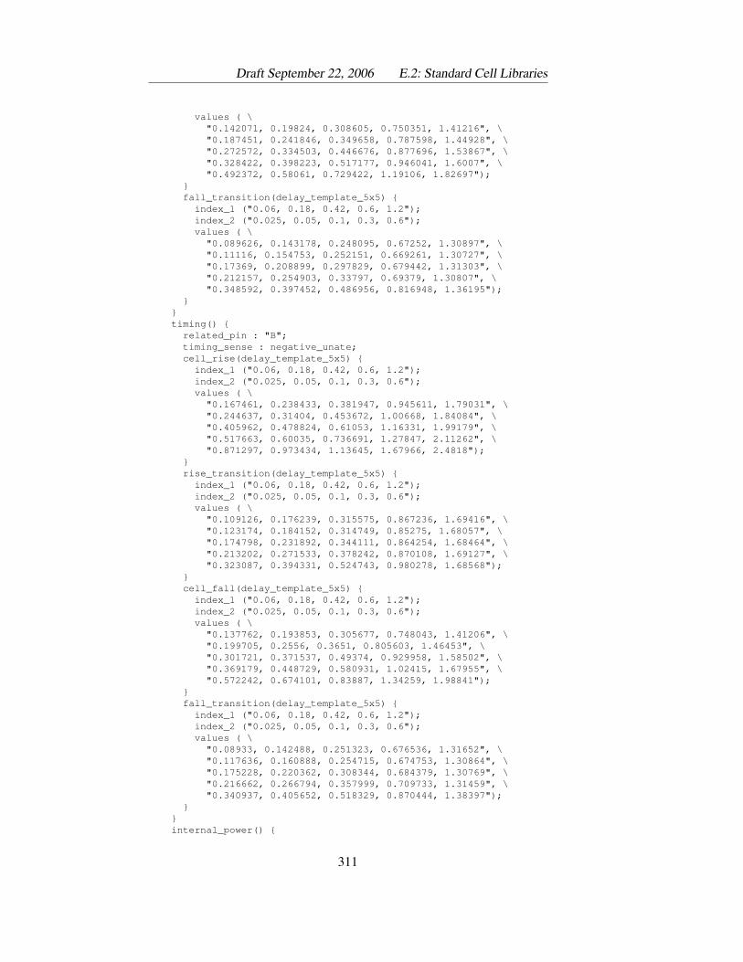
Draft September 22, 2006 E.2: Standard Cell Libraries
values ( \"0.142071, 0.19824, 0.308605, 0.750351, 1.41216", \"0.187451, 0.241846, 0.349658, 0.787598, 1.44928", \"0.272572, 0.334503, 0.446676, 0.877696, 1.53867", \"0.328422, 0.398223, 0.517177, 0.946041, 1.6007", \"0.492372, 0.58061, 0.729422, 1.19106, 1.82697");
}fall_transition(delay_template_5x5) {
index_1 ("0.06, 0.18, 0.42, 0.6, 1.2");index_2 ("0.025, 0.05, 0.1, 0.3, 0.6");values ( \
"0.089626, 0.143178, 0.248095, 0.67252, 1.30897", \"0.11116, 0.154753, 0.252151, 0.669261, 1.30727", \"0.17369, 0.208899, 0.297829, 0.679442, 1.31303", \"0.212157, 0.254903, 0.33797, 0.69379, 1.30807", \"0.348592, 0.397452, 0.486956, 0.816948, 1.36195");
}}timing() {
related_pin : "B";timing_sense : negative_unate;cell_rise(delay_template_5x5) {
index_1 ("0.06, 0.18, 0.42, 0.6, 1.2");index_2 ("0.025, 0.05, 0.1, 0.3, 0.6");values ( \
"0.167461, 0.238433, 0.381947, 0.945611, 1.79031", \"0.244637, 0.31404, 0.453672, 1.00668, 1.84084", \"0.405962, 0.478824, 0.61053, 1.16331, 1.99179", \"0.517663, 0.60035, 0.736691, 1.27847, 2.11262", \"0.871297, 0.973434, 1.13645, 1.67966, 2.4818");
}rise_transition(delay_template_5x5) {
index_1 ("0.06, 0.18, 0.42, 0.6, 1.2");index_2 ("0.025, 0.05, 0.1, 0.3, 0.6");values ( \
"0.109126, 0.176239, 0.315575, 0.867236, 1.69416", \"0.123174, 0.184152, 0.314749, 0.85275, 1.68057", \"0.174798, 0.231892, 0.344111, 0.864254, 1.68464", \"0.213202, 0.271533, 0.378242, 0.870108, 1.69127", \"0.323087, 0.394331, 0.524743, 0.980278, 1.68568");
}cell_fall(delay_template_5x5) {
index_1 ("0.06, 0.18, 0.42, 0.6, 1.2");index_2 ("0.025, 0.05, 0.1, 0.3, 0.6");values ( \
"0.137762, 0.193853, 0.305677, 0.748043, 1.41206", \"0.199705, 0.2556, 0.3651, 0.805603, 1.46453", \"0.301721, 0.371537, 0.49374, 0.929958, 1.58502", \"0.369179, 0.448729, 0.580931, 1.02415, 1.67955", \"0.572242, 0.674101, 0.83887, 1.34259, 1.98841");
}fall_transition(delay_template_5x5) {
index_1 ("0.06, 0.18, 0.42, 0.6, 1.2");index_2 ("0.025, 0.05, 0.1, 0.3, 0.6");values ( \
"0.08933, 0.142488, 0.251323, 0.676536, 1.31652", \"0.117636, 0.160888, 0.254715, 0.674753, 1.30864", \"0.175228, 0.220362, 0.308344, 0.684379, 1.30769", \"0.216662, 0.266794, 0.357999, 0.709733, 1.31459", \"0.340937, 0.405652, 0.518329, 0.870444, 1.38397");
}}internal_power() {
311
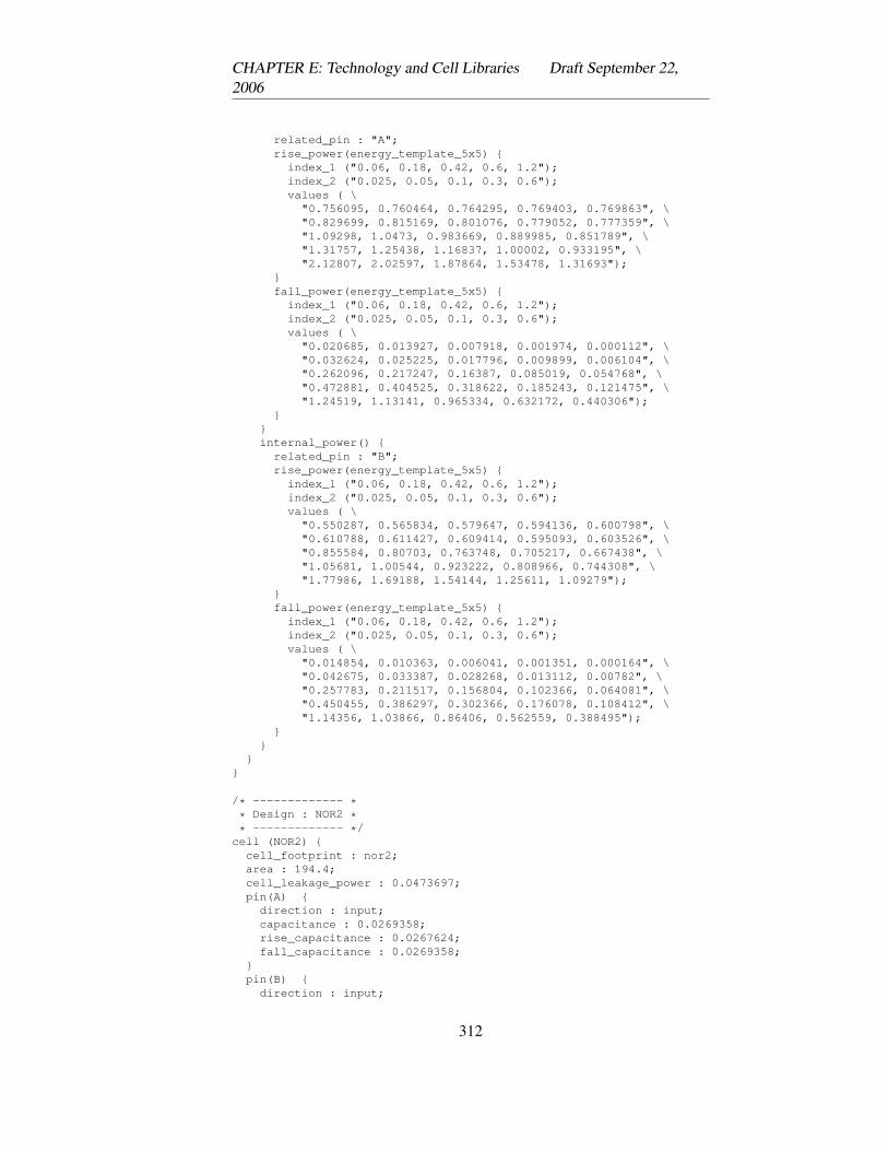
CHAPTER E: Technology and Cell Libraries Draft September 22,2006
related_pin : "A";rise_power(energy_template_5x5) {
index_1 ("0.06, 0.18, 0.42, 0.6, 1.2");index_2 ("0.025, 0.05, 0.1, 0.3, 0.6");values ( \
"0.756095, 0.760464, 0.764295, 0.769403, 0.769863", \"0.829699, 0.815169, 0.801076, 0.779052, 0.777359", \"1.09298, 1.0473, 0.983669, 0.889985, 0.851789", \"1.31757, 1.25438, 1.16837, 1.00002, 0.933195", \"2.12807, 2.02597, 1.87864, 1.53478, 1.31693");
}fall_power(energy_template_5x5) {
index_1 ("0.06, 0.18, 0.42, 0.6, 1.2");index_2 ("0.025, 0.05, 0.1, 0.3, 0.6");values ( \
"0.020685, 0.013927, 0.007918, 0.001974, 0.000112", \"0.032624, 0.025225, 0.017796, 0.009899, 0.006104", \"0.262096, 0.217247, 0.16387, 0.085019, 0.054768", \"0.472881, 0.404525, 0.318622, 0.185243, 0.121475", \"1.24519, 1.13141, 0.965334, 0.632172, 0.440306");
}}internal_power() {
related_pin : "B";rise_power(energy_template_5x5) {
index_1 ("0.06, 0.18, 0.42, 0.6, 1.2");index_2 ("0.025, 0.05, 0.1, 0.3, 0.6");values ( \
"0.550287, 0.565834, 0.579647, 0.594136, 0.600798", \"0.610788, 0.611427, 0.609414, 0.595093, 0.603526", \"0.855584, 0.80703, 0.763748, 0.705217, 0.667438", \"1.05681, 1.00544, 0.923222, 0.808966, 0.744308", \"1.77986, 1.69188, 1.54144, 1.25611, 1.09279");
}fall_power(energy_template_5x5) {
index_1 ("0.06, 0.18, 0.42, 0.6, 1.2");index_2 ("0.025, 0.05, 0.1, 0.3, 0.6");values ( \
"0.014854, 0.010363, 0.006041, 0.001351, 0.000164", \"0.042675, 0.033387, 0.028268, 0.013112, 0.00782", \"0.257783, 0.211517, 0.156804, 0.102366, 0.064081", \"0.450455, 0.386297, 0.302366, 0.176078, 0.108412", \"1.14356, 1.03866, 0.86406, 0.562559, 0.388495");
}}
}}
/* ------------- ** Design : NOR2 ** ------------- */
cell (NOR2) {cell_footprint : nor2;area : 194.4;cell_leakage_power : 0.0473697;pin(A) {
direction : input;capacitance : 0.0269358;rise_capacitance : 0.0267624;fall_capacitance : 0.0269358;
}pin(B) {
direction : input;
312
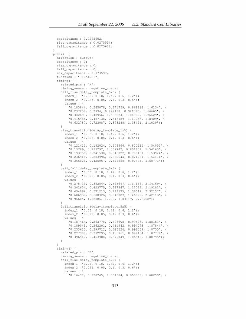
Draft September 22, 2006 E.2: Standard Cell Libraries
capacitance : 0.0275602;rise_capacitance : 0.0275514;fall_capacitance : 0.0275602;
}pin(Y) {
direction : output;capacitance : 0;rise_capacitance : 0;fall_capacitance : 0;max_capacitance : 0.373597;function : "(!(A+B))";timing() {
related_pin : "A";timing_sense : negative_unate;cell_rise(delay_template_5x5) {
index_1 ("0.06, 0.18, 0.42, 0.6, 1.2");index_2 ("0.025, 0.05, 0.1, 0.3, 0.6");values ( \
"0.183844, 0.245078, 0.371759, 0.868212, 1.6134", \"0.237238, 0.2994, 0.422118, 0.921395, 1.66665", \"0.342693, 0.40956, 0.533224, 1.01909, 1.76629", \"0.415486, 0.487138, 0.618189, 1.10243, 1.8409", \"0.632787, 0.723087, 0.878288, 1.38491, 2.1039");
}rise_transition(delay_template_5x5) {
index_1 ("0.06, 0.18, 0.42, 0.6, 1.2");index_2 ("0.025, 0.05, 0.1, 0.3, 0.6");values ( \
"0.121423, 0.182024, 0.304366, 0.800325, 1.54053", \"0.13789, 0.193297, 0.309742, 0.801601, 1.54163", \"0.193759, 0.241538, 0.343822, 0.798151, 1.53924", \"0.236946, 0.283996, 0.382544, 0.821731, 1.54114", \"0.366029, 0.425067, 0.526558, 0.92475, 1.58773");
}cell_fall(delay_template_5x5) {
index_1 ("0.06, 0.18, 0.42, 0.6, 1.2");index_2 ("0.025, 0.05, 0.1, 0.3, 0.6");values ( \
"0.278739, 0.362844, 0.525697, 1.17168, 2.14169", \"0.342634, 0.423775, 0.587347, 1.23026, 2.19202", \"0.494064, 0.571213, 0.729175, 1.36017, 2.32157", \"0.606937, 0.688326, 0.840887, 1.46929, 2.42113", \"0.96605, 1.05886, 1.229, 1.84119, 2.76968");
}fall_transition(delay_template_5x5) {
index_1 ("0.06, 0.18, 0.42, 0.6, 1.2");index_2 ("0.025, 0.05, 0.1, 0.3, 0.6");values ( \
"0.187464, 0.263778, 0.408608, 0.99623, 1.88153", \"0.189049, 0.262201, 0.411942, 0.994073, 1.87844", \"0.233625, 0.299712, 0.426524, 0.992569, 1.8755", \"0.277388, 0.332295, 0.455761, 0.999484, 1.87779", \"0.396547, 0.463908, 0.579049, 1.06549, 1.88795");
}}timing() {
related_pin : "B";timing_sense : negative_unate;cell_rise(delay_template_5x5) {
index_1 ("0.06, 0.18, 0.42, 0.6, 1.2");index_2 ("0.025, 0.05, 0.1, 0.3, 0.6");values ( \
"0.16477, 0.228745, 0.351394, 0.853889, 1.60259", \
313
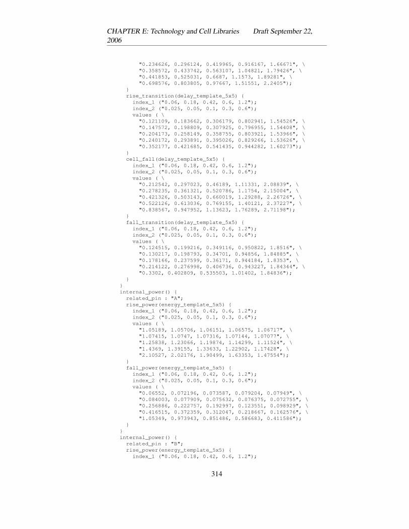
CHAPTER E: Technology and Cell Libraries Draft September 22,2006
"0.234626, 0.296124, 0.419965, 0.916167, 1.66671", \"0.358572, 0.433742, 0.563107, 1.04821, 1.79426", \"0.441853, 0.525031, 0.6687, 1.1573, 1.89281", \"0.698576, 0.803805, 0.97667, 1.51551, 2.2405");
}rise_transition(delay_template_5x5) {
index_1 ("0.06, 0.18, 0.42, 0.6, 1.2");index_2 ("0.025, 0.05, 0.1, 0.3, 0.6");values ( \
"0.121109, 0.183662, 0.306179, 0.802941, 1.54526", \"0.147572, 0.198809, 0.307925, 0.796955, 1.54408", \"0.204173, 0.258149, 0.358755, 0.803921, 1.53966", \"0.240172, 0.293891, 0.395026, 0.829266, 1.53626", \"0.352177, 0.421685, 0.541435, 0.944282, 1.60273");
}cell_fall(delay_template_5x5) {
index_1 ("0.06, 0.18, 0.42, 0.6, 1.2");index_2 ("0.025, 0.05, 0.1, 0.3, 0.6");values ( \
"0.212542, 0.297023, 0.46189, 1.11331, 2.08839", \"0.278235, 0.361321, 0.520786, 1.1754, 2.15004", \"0.421326, 0.503143, 0.660019, 1.29288, 2.26726", \"0.522126, 0.613036, 0.769155, 1.40121, 2.37227", \"0.838567, 0.947952, 1.13623, 1.76289, 2.71198");
}fall_transition(delay_template_5x5) {
index_1 ("0.06, 0.18, 0.42, 0.6, 1.2");index_2 ("0.025, 0.05, 0.1, 0.3, 0.6");values ( \
"0.124515, 0.199216, 0.349116, 0.950822, 1.8516", \"0.130217, 0.198793, 0.34701, 0.94856, 1.84885", \"0.178166, 0.237599, 0.36171, 0.944184, 1.8353", \"0.214122, 0.276998, 0.406736, 0.943227, 1.84344", \"0.3302, 0.402809, 0.535503, 1.01402, 1.84836");
}}internal_power() {
related_pin : "A";rise_power(energy_template_5x5) {
index_1 ("0.06, 0.18, 0.42, 0.6, 1.2");index_2 ("0.025, 0.05, 0.1, 0.3, 0.6");values ( \
"1.05189, 1.05706, 1.06151, 1.06575, 1.06717", \"1.07415, 1.0747, 1.07316, 1.07144, 1.07077", \"1.25838, 1.23066, 1.19874, 1.14299, 1.11524", \"1.4369, 1.39155, 1.33633, 1.22902, 1.17428", \"2.10527, 2.02176, 1.90499, 1.63353, 1.47554");
}fall_power(energy_template_5x5) {
index_1 ("0.06, 0.18, 0.42, 0.6, 1.2");index_2 ("0.025, 0.05, 0.1, 0.3, 0.6");values ( \
"0.06552, 0.072196, 0.073587, 0.079204, 0.07949", \"0.084003, 0.077909, 0.075632, 0.076375, 0.072755", \"0.256886, 0.222757, 0.192997, 0.123551, 0.098929", \"0.416515, 0.372359, 0.312047, 0.218667, 0.162576", \"1.05349, 0.973943, 0.851486, 0.586683, 0.411586");
}}internal_power() {
related_pin : "B";rise_power(energy_template_5x5) {
index_1 ("0.06, 0.18, 0.42, 0.6, 1.2");
314
Draft September 22, 2006 E.2: Standard Cell Libraries
index_2 ("0.025, 0.05, 0.1, 0.3, 0.6");values ( \
"0.667754, 0.675988, 0.683646, 0.691283, 0.693867", \"0.719271, 0.712559, 0.707625, 0.702077, 0.69958", \"0.926551, 0.891562, 0.844869, 0.774363, 0.746431", \"1.10078, 1.04962, 0.983575, 0.868654, 0.819274", \"1.73033, 1.64133, 1.5221, 1.26502, 1.08591");
}fall_power(energy_template_5x5) {
index_1 ("0.06, 0.18, 0.42, 0.6, 1.2");index_2 ("0.025, 0.05, 0.1, 0.3, 0.6");values ( \
"0.005916, 0.013655, 0.033371, 0.05336, 0.061535", \"0.016054, 0.021701, 0.027706, 0.056295, 0.066459", \"0.175386, 0.15036, 0.125382, 0.075668, 0.076332", \"0.327854, 0.287914, 0.225011, 0.173269, 0.133469", \"0.909317, 0.826504, 0.714023, 0.489888, 0.361315");
}}
}}
/* ------------- ** Design : XOR2 ** ------------- */
cell (XOR2) {cell_footprint : xor;area : 435.6;cell_leakage_power : 0.155716;pin(A) {
direction : input;capacitance : 0.0410345;rise_capacitance : 0.0408743;fall_capacitance : 0.0410345;
}pin(B) {
direction : input;capacitance : 0.0329048;rise_capacitance : 0.0329048;fall_capacitance : 0.0326434;
}pin(Y) {
direction : output;capacitance : 0;rise_capacitance : 0;fall_capacitance : 0;max_capacitance : 0.324837;function : "(AˆB)";timing() {
related_pin : "A";timing_sense : positive_unate;cell_rise(delay_template_5x5) {
index_1 ("0.06, 0.18, 0.42, 0.6, 1.2");index_2 ("0.025, 0.05, 0.1, 0.3, 0.6");values ( \
"0.40354, 0.48751, 0.658149, 1.33181, 2.32586", \"0.469359, 0.555491, 0.72558, 1.39742, 2.40751", \"0.597832, 0.680371, 0.848888, 1.51338, 2.5345", \"0.685781, 0.76766, 0.935746, 1.60461, 2.60613", \"0.963225, 1.04278, 1.20544, 1.86347, 2.86012");
}rise_transition(delay_template_5x5) {
index_1 ("0.06, 0.18, 0.42, 0.6, 1.2");
315
CHAPTER E: Technology and Cell Libraries Draft September 22,2006
index_2 ("0.025, 0.05, 0.1, 0.3, 0.6");values ( \
"0.211795, 0.291184, 0.456807, 1.12337, 2.11938", \"0.211911, 0.293037, 0.45754, 1.11561, 2.12514", \"0.21512, 0.295302, 0.458968, 1.12152, 2.12875", \"0.217536, 0.297565, 0.456529, 1.11754, 2.11137", \"0.232388, 0.304006, 0.461879, 1.11867, 2.11722");
}cell_fall(delay_template_5x5) {
index_1 ("0.06, 0.18, 0.42, 0.6, 1.2");index_2 ("0.025, 0.05, 0.1, 0.3, 0.6");values ( \
"0.307212, 0.364584, 0.47662, 0.920469, 1.57907", \"0.379443, 0.436377, 0.548701, 0.991159, 1.65171", \"0.510726, 0.567142, 0.678789, 1.1208, 1.78293", \"0.601508, 0.657431, 0.767435, 1.20688, 1.86378", \"0.881185, 0.936095, 1.04509, 1.47878, 2.13409");
}fall_transition(delay_template_5x5) {
index_1 ("0.06, 0.18, 0.42, 0.6, 1.2");index_2 ("0.025, 0.05, 0.1, 0.3, 0.6");values ( \
"0.144939, 0.19579, 0.299669, 0.721325, 1.35601", \"0.145614, 0.195997, 0.298851, 0.721534, 1.35722", \"0.152246, 0.201004, 0.300528, 0.720637, 1.35609", \"0.159564, 0.204742, 0.30478, 0.721762, 1.35783", \"0.184069, 0.225626, 0.317946, 0.724886, 1.35599");
}}timing() {
related_pin : "A";timing_sense : negative_unate;cell_rise(delay_template_5x5) {
index_1 ("0.06, 0.18, 0.42, 0.6, 1.2");index_2 ("0.025, 0.05, 0.1, 0.3, 0.6");values ( \
"0.282945, 0.368394, 0.536483, 1.207, 2.22446", \"0.335724, 0.41925, 0.587473, 1.26171, 2.25685", \"0.471919, 0.549543, 0.709427, 1.36776, 2.3629", \"0.580012, 0.658182, 0.811966, 1.46005, 2.44245", \"0.941867, 1.02505, 1.17677, 1.79312, 2.76057");
}rise_transition(delay_template_5x5) {
index_1 ("0.06, 0.18, 0.42, 0.6, 1.2");index_2 ("0.025, 0.05, 0.1, 0.3, 0.6");values ( \
"0.207182, 0.290401, 0.455769, 1.12095, 2.12807", \"0.211322, 0.292299, 0.457594, 1.12743, 2.1219", \"0.25387, 0.322817, 0.47062, 1.11956, 2.11598", \"0.296441, 0.359278, 0.497925, 1.1334, 2.1227", \"0.44896, 0.506227, 0.627816, 1.18529, 2.13535");
}cell_fall(delay_template_5x5) {
index_1 ("0.06, 0.18, 0.42, 0.6, 1.2");index_2 ("0.025, 0.05, 0.1, 0.3, 0.6");values ( \
"0.1945, 0.251131, 0.362632, 0.801988, 1.46899", \"0.238792, 0.294169, 0.404376, 0.843449, 1.50168", \"0.336019, 0.393262, 0.501386, 0.933009, 1.59269", \"0.40254, 0.466044, 0.576894, 1.00326, 1.6579", \"0.605956, 0.680629, 0.813363, 1.25476, 1.88819");
}fall_transition(delay_template_5x5) {
316
Draft September 22, 2006 E.2: Standard Cell Libraries
index_1 ("0.06, 0.18, 0.42, 0.6, 1.2");index_2 ("0.025, 0.05, 0.1, 0.3, 0.6");values ( \
"0.137514, 0.190448, 0.29471, 0.717977, 1.35154", \"0.151824, 0.198399, 0.297676, 0.718042, 1.34875", \"0.213049, 0.253712, 0.331862, 0.72214, 1.34876", \"0.270279, 0.302684, 0.377555, 0.737258, 1.35025", \"0.439119, 0.47713, 0.543666, 0.843778, 1.39461");
}}timing() {
related_pin : "B";timing_sense : positive_unate;cell_rise(delay_template_5x5) {
index_1 ("0.06, 0.18, 0.42, 0.6, 1.2");index_2 ("0.025, 0.05, 0.1, 0.3, 0.6");values ( \
"0.391823, 0.474551, 0.639514, 1.29872, 2.29675", \"0.456294, 0.538128, 0.703391, 1.36668, 2.3589", \"0.580221, 0.662308, 0.826394, 1.49287, 2.48674", \"0.6665, 0.747074, 0.914921, 1.57368, 2.58736", \"0.943287, 1.02576, 1.18974, 1.8483, 2.84977");
}rise_transition(delay_template_5x5) {
index_1 ("0.06, 0.18, 0.42, 0.6, 1.2");index_2 ("0.025, 0.05, 0.1, 0.3, 0.6");values ( \
"0.210564, 0.291176, 0.459109, 1.12102, 2.11951", \"0.210721, 0.291874, 0.459142, 1.11977, 2.12196", \"0.211906, 0.290901, 0.459151, 1.11868, 2.1203", \"0.205638, 0.287986, 0.453494, 1.12284, 2.12935", \"0.208787, 0.286936, 0.44953, 1.12024, 2.11038");
}cell_fall(delay_template_5x5) {
index_1 ("0.06, 0.18, 0.42, 0.6, 1.2");index_2 ("0.025, 0.05, 0.1, 0.3, 0.6");values ( \
"0.301085, 0.355224, 0.463674, 0.902025, 1.55616", \"0.373364, 0.42855, 0.538121, 0.974179, 1.62908", \"0.507425, 0.564003, 0.673071, 1.11006, 1.76385", \"0.6022, 0.658446, 0.767048, 1.20062, 1.85792", \"0.888034, 0.947065, 1.05859, 1.48963, 2.14068");
}fall_transition(delay_template_5x5) {
index_1 ("0.06, 0.18, 0.42, 0.6, 1.2");index_2 ("0.025, 0.05, 0.1, 0.3, 0.6");values ( \
"0.151095, 0.20006, 0.301684, 0.722589, 1.35493", \"0.151047, 0.200213, 0.301641, 0.720205, 1.3559", \"0.152622, 0.201965, 0.301931, 0.719524, 1.35583", \"0.150886, 0.201429, 0.30131, 0.720426, 1.35694", \"0.164885, 0.213123, 0.308122, 0.715558, 1.35096");
}}timing() {
related_pin : "B";timing_sense : negative_unate;cell_rise(delay_template_5x5) {
index_1 ("0.06, 0.18, 0.42, 0.6, 1.2");index_2 ("0.025, 0.05, 0.1, 0.3, 0.6");values ( \
"0.213389, 0.299892, 0.47158, 1.14955, 2.14616", \"0.28722, 0.369911, 0.539543, 1.21487, 2.21039", \
317
CHAPTER E: Technology and Cell Libraries Draft September 22,2006
"0.446394, 0.530453, 0.693418, 1.35317, 2.35062", \"0.559062, 0.65006, 0.815335, 1.46237, 2.45324", \"0.926596, 1.03178, 1.21478, 1.86263, 2.84289");
}rise_transition(delay_template_5x5) {
index_1 ("0.06, 0.18, 0.42, 0.6, 1.2");index_2 ("0.025, 0.05, 0.1, 0.3, 0.6");values ( \
"0.171194, 0.262528, 0.440739, 1.12312, 2.12148", \"0.180391, 0.26479, 0.437229, 1.11394, 2.1214", \"0.23249, 0.306842, 0.463139, 1.11619, 2.12434", \"0.268633, 0.346583, 0.496133, 1.12266, 2.11611", \"0.39086, 0.47366, 0.62649, 1.1904, 2.1364");
}cell_fall(delay_template_5x5) {
index_1 ("0.06, 0.18, 0.42, 0.6, 1.2");index_2 ("0.025, 0.05, 0.1, 0.3, 0.6");values ( \
"0.155423, 0.213066, 0.325072, 0.766739, 1.43034", \"0.218301, 0.274726, 0.385216, 0.828013, 1.48822", \"0.32392, 0.393804, 0.513401, 0.951286, 1.6129", \"0.393251, 0.471478, 0.602824, 1.04501, 1.69892", \"0.598843, 0.699711, 0.867402, 1.37058, 2.01845");
}fall_transition(delay_template_5x5) {
index_1 ("0.06, 0.18, 0.42, 0.6, 1.2");index_2 ("0.025, 0.05, 0.1, 0.3, 0.6");values ( \
"0.100729, 0.158082, 0.27006, 0.713622, 1.35491", \"0.120121, 0.168638, 0.272152, 0.711413, 1.3553", \"0.17847, 0.226784, 0.316668, 0.715387, 1.35014", \"0.22227, 0.273127, 0.364215, 0.74155, 1.3521", \"0.353261, 0.41712, 0.513182, 0.867976, 1.42573");
}}internal_power() {
related_pin : "A";rise_power(energy_template_5x5) {
index_1 ("0.06, 0.18, 0.42, 0.6, 1.2");index_2 ("0.025, 0.05, 0.1, 0.3, 0.6");values ( \
"0.695583, 0.698557, 0.702063, 0.706693, 0.708147", \"0.733875, 0.735163, 0.737759, 0.742688, 0.744758", \"0.908363, 0.902561, 0.89785, 0.894307, 0.894125", \"1.0696, 1.05668, 1.04936, 1.04017, 1.03742", \"1.67791, 1.64914, 1.61672, 1.57152, 1.55353");
}fall_power(energy_template_5x5) {
index_1 ("0.06, 0.18, 0.42, 0.6, 1.2");index_2 ("0.025, 0.05, 0.1, 0.3, 0.6");values ( \
"1.7795, 1.77961, 1.77982, 1.77974, 1.77943", \"1.83505, 1.83401, 1.83292, 1.83152, 1.83101", \"2.04274, 2.03514, 2.02718, 2.01761, 2.01391", \"2.21712, 2.20181, 2.18772, 2.16877, 2.16174", \"2.85473, 2.82256, 2.78257, 2.73116, 2.71032");
}}internal_power() {
related_pin : "B";rise_power(energy_template_5x5) {
index_1 ("0.06, 0.18, 0.42, 0.6, 1.2");index_2 ("0.025, 0.05, 0.1, 0.3, 0.6");
318

Draft September 22, 2006 E.2: Standard Cell Libraries
values ( \"0.909205, 0.891335, 0.860428, 0.801975, 0.773157", \"0.9407, 0.921619, 0.897854, 0.840689, 0.811164", \"1.0877, 1.07101, 1.04917, 1.00039, 0.970295", \"1.23848, 1.2189, 1.19619, 1.14715, 1.11437", \"1.81977, 1.79509, 1.75013, 1.68965, 1.64867");
}fall_power(energy_template_5x5) {
index_1 ("0.06, 0.18, 0.42, 0.6, 1.2");index_2 ("0.025, 0.05, 0.1, 0.3, 0.6");values ( \
"1.53763, 1.51396, 1.48449, 1.43919, 1.41753", \"1.5962, 1.57353, 1.54491, 1.49778, 1.47545", \"1.79854, 1.77641, 1.74815, 1.6933, 1.66383", \"1.96593, 1.94916, 1.91642, 1.85718, 1.82273", \"2.57484, 2.54471, 2.50257, 2.42655, 2.37882");
}}
}}
}
E.2.2 UofU Digital
E.2.3 UofU Async
E.2.4 OSU Libraries
319

CHAPTER E: Technology and Cell Libraries Draft September 22,2006
320
Compact yet High-Performance (CyHP) Library for Short Time-to-Market with New Technologies
Nguyen Minh Duc and Takayasu Sakurai
Center for Collaborative Research and Institute of Industrial Science University of Tokyo
7-22-1 Roppongi, Minato-ku, Tokyo, 106-8558, JAPAN Tel: +81-3-3402-6226 Fax: +81-3-3402-6227
e-mail: [email protected], [email protected]
Abstract Two compact yet high performance standard cell
libraries (CyHP libraries), which contain only 11111111 and 20 cells
respectively, are proposed. The first CyHP library leads to 5%
increase in delay compared to a library containing about 400 cells.
The second CyHP library suppresses delay increase up to 2%. The
compact nature of these libraries not only reduces the cost and time
for generation and maintenance substantially (thus enables new
technologies to be adopted immediately), but also shortens synthesis
time to about a half. Application results of these libraries to standard
benchmarks and an industry design of about 80K gates are
presented.
I. INTRODUCTION
Standard cell based design has become a mainstream design
style for recent VLSI’s. Standard cell libraries are getting bigger,
containing more than 500 cells in expecting better performance
of the resulting VLSI's. Generating, verifying and maintaining
these big libraries, however, need lot of time and manpower and
errors may be crept into the cell designs and/or cell
characterization processes. Moreover, technologies are getting
diverse and changing rapidly and a cell library must be generated
from scratch more frequently. For example, low-power
technologies such as MTCMOS, VTCMOS, DTMOS, and
partially-depleted SOI [1] demand new layout and templates for
the cells should be redesigned. To make the most of the more
interconnection levels, self-aligned contacts, and other
technology innovations, new cell design is required. These new
cells cannot be generated by just changing the parameters of the
parameterized cell templates. In this sense, the burden of the big
cell libraries becomes an obstacle to realize short time-to-market
of VLSI's.
Considering these issues, this paper proposes two compact
yet high performance cell libraries (CyHP libraries) that contain
fewer cells and is inherently efficient in generation, verification
and maintenance. The drawback in adopting the small libraries
may be area increase, delay increase, power increase and
synthesis time increase.
Using multiple cell libraries, a widely used synthesis tool
(Synopsys Design Compiler), a large set of benchmark circuits
and a real industrial design, the paper shows the increase in these
indices can be small and the synthesis time is even decreased to
about a half. The area and power increase are not very important,
because synthesized blocks by standard cells are only a part of
the VLSI and memories, I/O's, clock systems and handcrafted
datapaths occupy major portion of the area and power in most
VLSI designs. The delay is important because the critical path in
a synthesized block may determine the clock frequency of the
total chip even though it is not major area-wise. The delay with
the compact library, however, increases only about 2% even if the
number of cells in a library is decreased to 20.
Since it is possible to make use of new technologies earlier
with the compact libraries, it may achieve better overall
performance at a fixed time point, although small increase in
delay is observed if the same technology is used. The compact
libraries will be beneficial to semiconductor suppliers as well as
design houses that create their own set of standard cells from time
to time to be independent from foundries.
In section II, an algorithm used to determine the CyHP
libraries are explained. Section III shows the delay, area, power,
and synthesis time results achieved with the CyHP libraries
produced by this algorithm. An application of the CyHP libraries
to an industry design is given in section IV.
II. ALGORITHM TO DETERMINE CELL SET
Generally there is no fixed rule to determine which cells a
standard cell library should contain and the organization of a
library is often determined in an empirical way. In this study,
compact libraries are created by removing cells from existing
libraries such that the increase of delay, area and power of the
circuits generated automatically is kept as small as possible.
A standard cell library usually contains hundreds of cells.
However, most of them do not influence much the performance
(i.e. delay, area and power. Hereafter, performance will be used
as a generic term to indicate these indices) of the circuit being
synthesized. While primitive cells such as inverter, NAND, NOR,
etc. are used very frequently, cells with relatively complicated
functionality such as AND-OR-INV, majority circuit, and 8-input
MUX are seldom used in random logic design. The circuit
performance is almost unchanged even if these infrequently used
cells are eliminated from the library. A more compact library can
be obtained by removing these cells from an existing library. The
problems is which cells to remove and what is the performance
penalty occurs due to the absent of these cells.
When a cell is removed from the library, the target circuit is
reconstructed by using other cells. The degree of circuit
reconstruction depends on both functionality of the removed cell
and its occurrence in the circuit. The more complicated the
functionality of the removed cell is, the larger portion of the
circuit needs to be reconstructed. Removing a cell that is used
frequently will also lead to extensive reconstruction. Since
complex cells always have large area, cell area times its
occurrence (i.e. the area occupied by a cell in the entire circuit)
can be used as a parameter to measure quantitatively its effect on
the circuit structure. On the other hand, the circuit performance is
almost unchanged if the change in the reconstruction is
insignificant. Thus, the smaller the area occupied by a cell in a
circuit, the less significant the effect of that cell to the circuit is.
The cell with the smallest area is least important in terms of
performance of the synthesized circuit.
Removing an appropriate number of least important cells
from an existing library results in a new library, which has less
cells than the original one but does not deteriorate much the
performance of the circuit constructed by using the library. The
above-mentioned procedure can be used as a heuristic rule to
reduce cells of a library. The area occupied by a cell, however,
depends on the nature of the circuit itself as well as the algorithm
of the logic synthesis tool. Its average value over a large set of
benchmark circuits should be used to guarantee the generality of
the resulting library. In this study, the ISCAS89 benchmark set
[2] is employed. This benchmark set consists of 31 sequential
circuits, whose scales range from hundreds to around 20K gates.
The average area portion occupied by a cell is calculated as
following.
∑=
×=
BN
i i
i
B Aaf
Na
1
1 , (1)
where NB (31 in this case) is the number of benchmark circuits, fi
is the occurrence of the cell in the i-th circuit, a is the cell area
and Ai is the total area of the i-th circuit.
The flowchart of the library compacting algorithm is shown
in Fig. 1. An existing standard cell library and a set of benchmark
circuits are used as the input. The algorithm can be divided into
the following steps.
1. Synthesize (and optimize) all benchmark circuits using the
original library L.
2. Analyze the circuits generated and use equation (1) to
calculate the average area a_ occupied by each cell in L.
3. Remove s cells with the smallest a_ from L (s is an
appropriate integer).
4. If L contains the minimum cell set required for synthesis, go
to step 1. Otherwise stop.
The number of cells in L is reduced by s each time steps 1
through 3 are executed. A minimum cell set (normally an inverter,
a 2-input NOR and a flip-flop are required) must exist in L to
make the synthesis in step 1 possible. L becomes more and more
compact as long as the execution proceeds. The algorithm will
stop when one of these minimum cells is excluded from L. The
logic synthesizer used in this study is a widely used commercial
tool [3]. In step 2, the area, delay and power used to calculate a_
are the values produced by the logic synthesizer. These values are
used by designers to estimate performance of the synthesized
circuits. The optimization in step 1 is done in a delay-oriented
way, i.e. constraints are set such that the fastest circuits are
generated (however, the result does not change if optimization is
done in an area-oriented way, i.e. constraints are set such that the
smallest circuits are produced).
With a given library containing a large number of cells, the
above algorithm produces (in step 3) a series of libraries that have
different number of cells. These libraries can be arranged in the
order they are produced as L, L1, L2, …, Lm (m is the number of
times that steps 1 through 3 are iterated). L is the original library
and also the largest one in this series. Lm is the last and most
compact library that is obtained just before the algorithm halts.
The number of cells of Li+1 is less than that of Li by s at least
(since removing a cell from the library generally cause some
other cells be unused). Let Pj and Pij be the performance (which
is one of delay, area and power as stated above) of the j-th
benchmark circuit when using the original library L and the i-th
library (i.e. Li) in this series respectively. The relative
performance of the j-th Cho circuit achieved with Li can be
defined as,
j
ijij P
Pp = (2)
The average of relative performance of all benchmark
circuits then can be expressed as following.
∑ ∑= =
==B BN
j
N
j j
ij
Bij
Bi P
PN
pN
p1 1
11 (3)
The relation between the number of cells and performance is
obtained by calculating pi
_ for each library Li . There exists a
trade-off between pi
_ and the number of cells contained in Li.
Generally, decreasing the number of cells will increase pi
_ (i.e.
deteriorates the circuit performance). A CyHP library with a
small number of cells and an adequate performance can be
achieved by examining carefully this trade-off.
III. RESULTS
Based on the algorithm described in the previous section, an
automated library generating system was implemented using Perl
[4]. The number of cells removed each time, s, should be set to 1
in order to achieve a precise performance versus number of cells
curve. However, as shown later, the performance stays almost
constant when the number of cells is larger than 40. Thus, the
calculation time can be reduced greatly by setting s to a big initial
SYNTHESIZABLE?SYNTHESIZABLE?SYNTHESIZABLE?SYNTHESIZABLE?
STARTSTARTSTARTSTART
SYNTHESIZE ALLSYNTHESIZE ALLSYNTHESIZE ALLSYNTHESIZE ALLBENCHMARK CIRCUITSBENCHMARK CIRCUITSBENCHMARK CIRCUITSBENCHMARK CIRCUITS
ANALYZE RESULTSANALYZE RESULTSANALYZE RESULTSANALYZE RESULTS
REMOVE S CELLS WITHREMOVE S CELLS WITHREMOVE S CELLS WITHREMOVE S CELLS WITHTHE SMALLEST AREATHE SMALLEST AREATHE SMALLEST AREATHE SMALLEST AREA
STOPSTOPSTOPSTOP
YESYESYESYES
NONONONO
Fig. 1 Flowchart of library compacting algorithm.
value (e.g. tens) then decreasing s gradually as the number of
cells decreases.
Three libraries A, B and C are used as the starting library.
They are all from different companies and have different design
rules (1.5[µm], 0.6[µm] and 0.25[µm]). This means that they are
very different in nature and the results gained from the
experiments using these three libraries will be applying to any
other libraries.
All these three libraries contain around 400 cells and are
used actually in commercial and academic LSI designs. It takes
more than a week to complete calculation for one library using a
400 MHz Sun Enterprise 450 workstation. The variation of delay,
area and power versus the number of cells are shown in Figs. 2, 3
and 4 respectively. The horizontal axis signifies the number of
cells. Delay, area and power are calculated using equation (3).
In addition to delay, area and power, the average time to
synthesize each benchmark is also plotted in Fig. 5 (the synthesis
time is calculated in a similar fashion using equation (3)).
Three libraries show the same tendency. In both three cases,
the number of cells ranges between around 150 and 10. The
maximum number of cells (about 150, which is the right most
value of the curves in Figs. 2, 3, 4 and 5) is much less than the
number of cells available in the original libraries. This means that
the remaining 250 cells are left unused in this case.
It can be observed that the circuit performance is almost
constant when the library contains more than 20 cells. Increase in
delay is almost negligible, irrelevant to the number of cells. Area
and power begin to increase considerably when the number of
cells becomes less than 20. Even when the library has only 10
cells, delay, area and power increase no more than 5%, 30% and
40% respectively.
In contrast to performance, synthesis time varies irregularly.
However, synthesis time tends to decrease when the number of
cells is small.
The curves in Figs. 2, 3, and 4 show that the library with a number of cells between 10 and 20 is the appropriate CyHP
Number of cellsNumber of cellsNumber of cellsNumber of cells
Dela
yD
ela
yD
ela
yD
ela
y
0000
0.20.20.20.2
0.40.40.40.4
0.60.60.60.6
0.80.80.80.8
1111
1.21.21.21.2
1.41.41.41.4
1.61.61.61.6
1.81.81.81.8
2222
0000 20202020 40404040 60606060 80808080 100100100100 120120120120 140140140140 160160160160
library Alibrary Alibrary Alibrary Alibrary Blibrary Blibrary Blibrary Blibrary Clibrary Clibrary Clibrary C
Fig. 2 Average of relative delay versus number of cells.
Are
aA
rea
Are
aA
rea
0000
0.20.20.20.2
0.40.40.40.4
0.60.60.60.6
0.80.80.80.8
1111
1.21.21.21.2
1.41.41.41.4
1.61.61.61.6
1.81.81.81.8
2222
0000 20202020 40404040 60606060 80808080 100100100100 120120120120 140140140140 160160160160
library Alibrary Alibrary Alibrary Alibrary Blibrary Blibrary Blibrary Blibrary Clibrary Clibrary Clibrary C
Number of cellsNumber of cellsNumber of cellsNumber of cells Fig. 3 Average of relative area versus number of cells.
Pow
er
Pow
er
Pow
er
Pow
er
0000
0.20.20.20.2
0.40.40.40.4
0.60.60.60.6
0.80.80.80.8
1111
1.21.21.21.2
1.41.41.41.4
1.61.61.61.6
1.81.81.81.8
2222
0000 20202020 40404040 60606060 80808080 100100100100 120120120120 140140140140 160160160160
library Alibrary Alibrary Alibrary Alibrary Blibrary Blibrary Blibrary Blibrary Clibrary Clibrary Clibrary C
Number of cellsNumber of cellsNumber of cellsNumber of cells Fig. 4 Average of relative power versus number of cells.
Syn
thesi
s tim
eS
ynth
esi
s tim
eS
ynth
esi
s tim
eS
ynth
esi
s tim
e
0000 20202020 40404040 60606060 80808080 100100100100 120120120120 140140140140 1601601601600000
0.20.20.20.2
0.40.40.40.4
0.60.60.60.6
0.80.80.80.8
1111
1.21.21.21.2
1.41.41.41.4
1.61.61.61.6
1.81.81.81.8
2222
library Alibrary Alibrary Alibrary Alibrary Blibrary Blibrary Blibrary Blibrary Clibrary Clibrary Clibrary C
Number of cellsNumber of cellsNumber of cellsNumber of cells Fig. 5 Average of relative synthesis time versus number of cells.
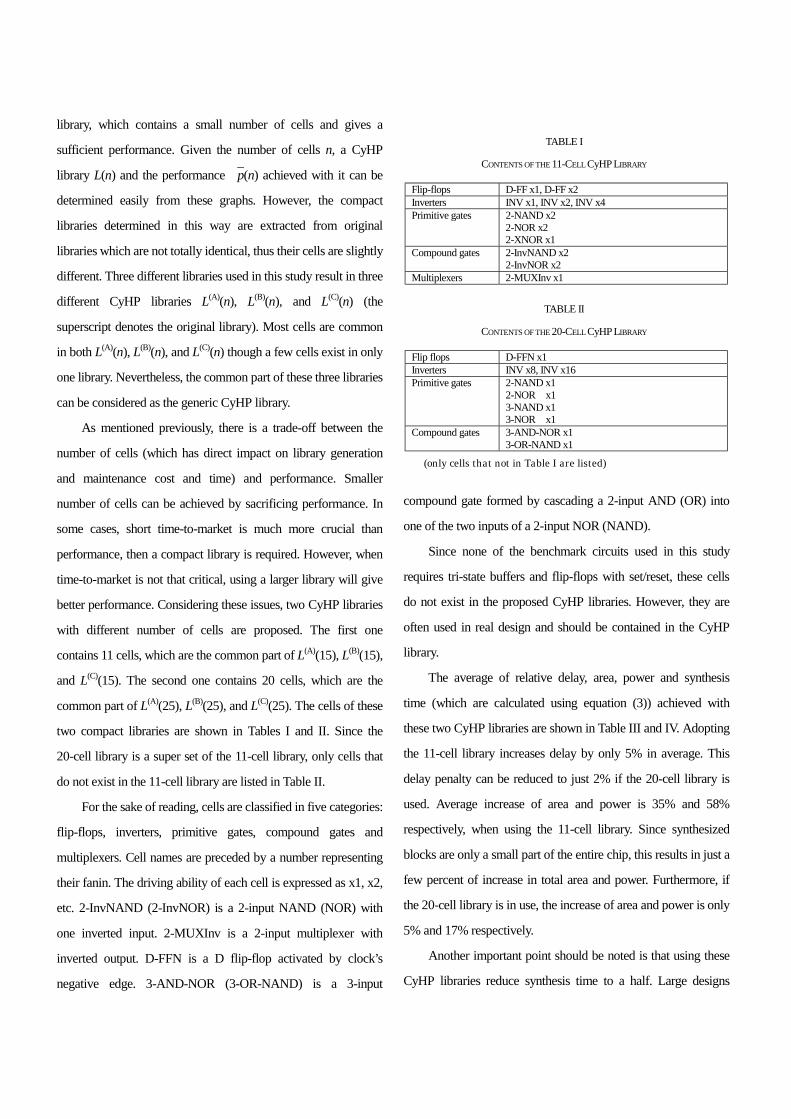
library, which contains a small number of cells and gives a
sufficient performance. Given the number of cells n, a CyHP
library L(n) and the performance p_(n) achieved with it can be
determined easily from these graphs. However, the compact
libraries determined in this way are extracted from original
libraries which are not totally identical, thus their cells are slightly
different. Three different libraries used in this study result in three
different CyHP libraries L(A)(n), L(B)(n), and L(C)(n) (the
superscript denotes the original library). Most cells are common
in both L(A)(n), L(B)(n), and L(C)(n) though a few cells exist in only
one library. Nevertheless, the common part of these three libraries
can be considered as the generic CyHP library.
As mentioned previously, there is a trade-off between the
number of cells (which has direct impact on library generation
and maintenance cost and time) and performance. Smaller
number of cells can be achieved by sacrificing performance. In
some cases, short time-to-market is much more crucial than
performance, then a compact library is required. However, when
time-to-market is not that critical, using a larger library will give
better performance. Considering these issues, two CyHP libraries
with different number of cells are proposed. The first one
contains 11 cells, which are the common part of L(A)(15), L(B)(15),
and L(C)(15). The second one contains 20 cells, which are the
common part of L(A)(25), L(B)(25), and L(C)(25). The cells of these
two compact libraries are shown in Tables I and II. Since the
20-cell library is a super set of the 11-cell library, only cells that
do not exist in the 11-cell library are listed in Table II.
For the sake of reading, cells are classified in five categories:
flip-flops, inverters, primitive gates, compound gates and
multiplexers. Cell names are preceded by a number representing
their fanin. The driving ability of each cell is expressed as x1, x2,
etc. 2-InvNAND (2-InvNOR) is a 2-input NAND (NOR) with
one inverted input. 2-MUXInv is a 2-input multiplexer with
inverted output. D-FFN is a D flip-flop activated by clock’s
negative edge. 3-AND-NOR (3-OR-NAND) is a 3-input
compound gate formed by cascading a 2-input AND (OR) into
one of the two inputs of a 2-input NOR (NAND).
Since none of the benchmark circuits used in this study
requires tri-state buffers and flip-flops with set/reset, these cells
do not exist in the proposed CyHP libraries. However, they are
often used in real design and should be contained in the CyHP
library.
The average of relative delay, area, power and synthesis
time (which are calculated using equation (3)) achieved with
these two CyHP libraries are shown in Table III and IV. Adopting
the 11-cell library increases delay by only 5% in average. This
delay penalty can be reduced to just 2% if the 20-cell library is
used. Average increase of area and power is 35% and 58%
respectively, when using the 11-cell library. Since synthesized
blocks are only a small part of the entire chip, this results in just a
few percent of increase in total area and power. Furthermore, if
the 20-cell library is in use, the increase of area and power is only
5% and 17% respectively.
Another important point should be noted is that using these
CyHP libraries reduce synthesis time to a half. Large designs
TABLE I
CONTENTS OF THE 11-CELL CyHP LIBRARY
Flip-flops D-FF x1, D-FF x2 Inverters INV x1, INV x2, INV x4 Primitive gates 2-NAND x2
2-NOR x2 2-XNOR x1
Compound gates 2-InvNAND x2 2-InvNOR x2
Multiplexers 2-MUXInv x1
TABLE II
CONTENTS OF THE 20-CELL CyHP LIBRARY
Flip flops D-FFN x1 Inverters INV x8, INV x16 Primitive gates 2-NAND x1
2-NOR x1 3-NAND x1 3-NOR x1
Compound gates 3-AND-NOR x1 3-OR-NAND x1
(only cells that not in Table I are listed)
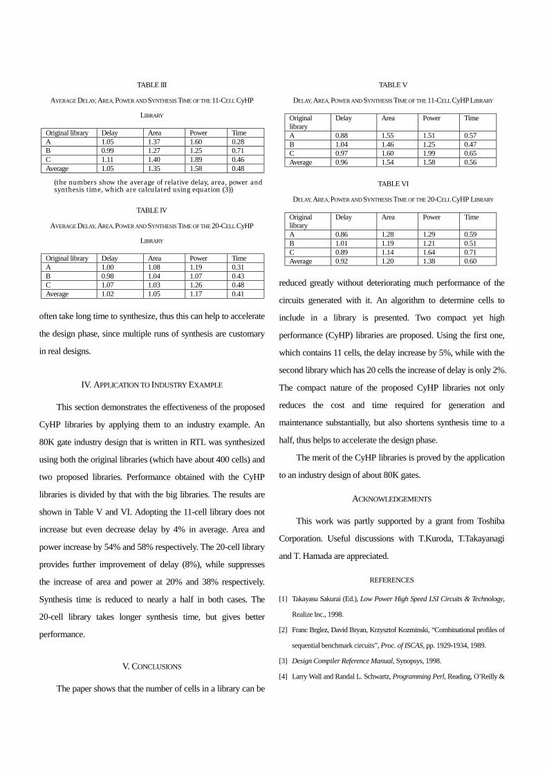
often take long time to synthesize, thus this can help to accelerate
the design phase, since multiple runs of synthesis are customary
in real designs.
IV. APPLICATION TO INDUSTRY EXAMPLE
This section demonstrates the effectiveness of the proposed
CyHP libraries by applying them to an industry example. An
80K gate industry design that is written in RTL was synthesized
using both the original libraries (which have about 400 cells) and
two proposed libraries. Performance obtained with the CyHP
libraries is divided by that with the big libraries. The results are
shown in Table V and VI. Adopting the 11-cell library does not
increase but even decrease delay by 4% in average. Area and
power increase by 54% and 58% respectively. The 20-cell library
provides further improvement of delay (8%), while suppresses
the increase of area and power at 20% and 38% respectively.
Synthesis time is reduced to nearly a half in both cases. The
20-cell library takes longer synthesis time, but gives better
performance.
V. CONCLUSIONS
The paper shows that the number of cells in a library can be
reduced greatly without deteriorating much performance of the
circuits generated with it. An algorithm to determine cells to
include in a library is presented. Two compact yet high
performance (CyHP) libraries are proposed. Using the first one,
which contains 11 cells, the delay increase by 5%, while with the
second library which has 20 cells the increase of delay is only 2%.
The compact nature of the proposed CyHP libraries not only
reduces the cost and time required for generation and
maintenance substantially, but also shortens synthesis time to a
half, thus helps to accelerate the design phase.
The merit of the CyHP libraries is proved by the application
to an industry design of about 80K gates.
ACKNOWLEDGEMENTS
This work was partly supported by a grant from Toshiba
Corporation. Useful discussions with T.Kuroda, T.Takayanagi
and T. Hamada are appreciated.
REFERENCES
[1] Takayasu Sakurai (Ed.), Low Power High Speed LSI Circuits & Technology,
Realize Inc., 1998.
[2] Franc Brglez, David Bryan, Krzysztof Kozminski, “Combinational profiles of
sequential benchmark circuits”, Proc. of ISCAS, pp. 1929-1934, 1989.
[3] Design Compiler Reference Manual, Synopsys, 1998.
[4] Larry Wall and Randal L. Schwartz, Programming Perl, Reading, O’Reilly &
TABLE V
DELAY, AREA, POWER AND SYNTHESIS TIME OF THE 11-CELL CyHP LIBRARY
Original library
Delay Area Power Time
A 0.88 1.55 1.51 0.57 B 1.04 1.46 1.25 0.47 C 0.97 1.60 1.99 0.65 Average 0.96 1.54 1.58 0.56
TABLE VI
DELAY, AREA, POWER AND SYNTHESIS TIME OF THE 20-CELL CyHP LIBRARY
Original library
Delay Area Power Time
A 0.86 1.28 1.29 0.59 B 1.01 1.19 1.21 0.51 C 0.89 1.14 1.64 0.71 Average 0.92 1.20 1.38 0.60
TABLE III
AVERAGE DELAY, AREA, POWER AND SYNTHESIS TIME OF THE 11-CELL CyHP
LIBRARY
Original library Delay Area Power Time A 1.05 1.37 1.60 0.28 B 0.99 1.27 1.25 0.71 C 1.11 1.40 1.89 0.46 Average 1.05 1.35 1.58 0.48
(the numbers show the average of relative delay, area, power and synthesis time, which are calculated using equation (3))
TABLE IV
AVERAGE DELAY, AREA, POWER AND SYNTHESIS TIME OF THE 20-CELL CyHP
LIBRARY
Original library Delay Area Power Time A 1.00 1.08 1.19 0.31 B 0.98 1.04 1.07 0.43 C 1.07 1.03 1.26 0.48 Average 1.02 1.05 1.17 0.41

Associates Inc., 1991.