vol. 3, special issue 5, december 2014 single phase power ... · single phase power factor...
TRANSCRIPT

ISSN (Print) : 2320 – 3765
ISSN (Online): 2278 – 8875
International Journal of Advanced Research in Electrical,
Electronics and Instrumentation Engineering
(An ISO 3297: 2007 Certified Organization)
Vol. 3, Special Issue 5, December 2014
Copyright to IJAREEIE www.ijareeie.com 610
Single Phase Power Factor Correction
Based on Averaged Current Mode
Controlled Boost Converter
Blessen Antony Francis1, Bos Mathew Jos
2, Babu Thomas
3
Department of Electrical and Electronics Engineering, Mar Athanasius College of Engineering, Kothamangalam,
Kerala, India1, 2,3
.
ABSTRACT: The conventional full-wave diode bridge rectifier with an output capacitor filter produces current spikes
in the supply, thus lowering the power factor and distorting the waveform. An ideal rectifier presents an effective
resistive load (Emulated resistance) to the AC power line; hence, if the supplied AC voltage is sinusoidal, then the
current drawn by the rectifier is also sinusoidal and is in phase with the voltage. Converters that approximate the
properties of the ideal rectifier are sometimes called power factor corrected, because their input power factor is nearly
unity. The boost converter, as well as a variety of other converters, can be controlled such that a near ideal rectifier
system is obtained. This is accomplished by control of a high-frequency switching converter, such that the ac line
current waveform follows the applied ac line voltage. The boost converter is operated in Continuous Conduction Mode
(CCM), and controlled by Average Current Mode Control (ACMC). The system contains multi-loop control strategy
and a feed-forward loop in order to get power factor near unity with constant output power. There are a variety of
Power Factor Correction (PFC) chips available in the market, one being the UC3854, can be operated in Average
Current Mode Control. The simulation of a 250W, AC – DC rectified system with Unity Power Factor at the input
using UC3854 was done in PSIM Power Electronics simulation software and results were obtained.
KEYWORDS:PFC-Power Factor Correction, CCM-Continuous Conduction Mode, ACMC-Average Current Mode
control, CMC- Current Mode Control, PWM – Pulse Width Modulation, PI – Proportional plus Integral
I. INTRODUCTION
.AC to DC conversion basically requires a diode bridge and a filter capacitor. An increase in the power requirement
and the betterment of DC output, demands large value of capacitors. This increases the non-sinusoidal current from the
supply. The RMS value of current increase and there is a chance of tripping of the supply. Moreover, this non-
sinusoidal current is an indication of harmonic content assuming sinusoidal supply voltage, and the power factor
decreases [2, 3]. As the power factor decrease, the drawing of useful power decrease. Harmonics increase conduction
losses. Hence, it is important to improve power factor and owing to this importance, standards were designed for
regulating line current harmonics. There are passive and active power factor correction methods [1].
The method of power factor correction used here is the active type and it is current mode control. The current mode
control (CMC) strategy used is the averaged current mode control, which is an extension of the peak CMC. Peak CMC
is discussed in detail [4], with modelling of the same, and a basic control system block diagram provided, which form
the basic idea. Peak current control is the control of the peak current through the switching element. Peak current mode
control requires an additional ramp for stability, there is no need for current loop compensation.
When the ripple in the inductor current is less, peak current mode becomes similar to average current mode control
(ACMC). Here, the average current through the inductor is sensed. Any current can be controlled using this method.
Average CMC require two loops viz. a fast current loop(Large bandwidth), and comparatively low band width voltage
loop. Paper [5] is a continuation of [4], explaining additional blocks in the control system modelling of average CMC

ISSN (Print) : 2320 – 3765
ISSN (Online): 2278 – 8875
International Journal of Advanced Research in Electrical,
Electronics and Instrumentation Engineering
(An ISO 3297: 2007 Certified Organization)
Vol. 3, Special Issue 5, December 2014
Copyright to IJAREEIE www.ijareeie.com 611
when compared to the peak CMC. The control system modelling of ACMC in [6] is done by modelling the PWM
switch, and a buck converter is explained.
In paper [7], the issues of peak CMC, the current loop design for an average CMC in a buck converter, a boost pre-
regulator and a flyback regulator, and different practical aspects of current sensing are discussed. The current loop
transfer function and control loop design for this work is obtained from this reference [7]. Paper [8] discusses about the
voltage loop modelling and transfer function of the boost PFC circuit, and provides different transfer functions for
resistive load and a constant power load to the boost PFC circuit. When we are connecting a constant power load, i.e., a
DC-DC converter, the constant power load represents a negative resistive load. Hence, a constant power load should
not be connected to the boost PFC unless it is tightly regulated (close-loop controlled).
The basic pre-regulator operation, presence double line frequency component at the output, different power circuit
topologies for PFC, control loop design criteria, the need of a input voltage feed-forward loop for PFC, average CMC
design, small signal model of voltage loop can be found in [9], which is an extension of [8]. The paper also gives some
valuable suggestions on load over current limiting and practical aspects of control circuit DC offsets. [10] Discusses
about peak and average CMC control of boost PFC circuit. An in-site to current loop compensation procedure is
provided. [11] Provides small signal model of the required average CMC boost PFC circuit. The block diagram
provided can be read as an extension from [4] and [5]. The modelling of the multiplier is done [11] and is incorporated
into the work of [5]. The current and voltage loop transfer functions, the design guidelines for the compensation of the
same for the thesis work are obtained from this reference.
[13]Discusses the sources of harmonic distortion in boost PFC circuit, an initial design example of the boost
converter, setting up of the multiplier and divider, voltage loop and feed-forward loop design guidelines. Sources of
harmonic distortion in the PFC circuit, and the ways to reduce the same can be obtained from [12]. Important aspects
on practical design issues for PFC circuits, especially on-line filtering, loop compensation, input voltage feed-forward,
protection circuits and the need for switching signal synchronisation (meant for constant power load) are addressed in
[14].
[15]Introduces the UC3854 power factor correction chip for average CMC boost PFC circuit, which forms the heart
of the work.[16] Provides guidelines on using the chip, and [17] provides steps for protection and optimisation of the
boost PFC circuit. [18] Provides in-site for physical implementation of compensator design based on op-amps.
The design and simulation of a 250 W, AC-DC converter is carried out, with 400VDC obtained at the output. The
simulation is done using a resistive load, and then with a closed loop 385 V/ 50V, 5A (250 W) DC-DC buck converter.
The controller for buck converter can be used for forward converter (A buck converter derivative, with turns ratio 1:1)
also, in case isolation is required. The simulation is done for similar load conditions for resistive and constant load
converter loads. The control system design was done with the aid of MATLAB Version 7.10 (R2010b). Simulation of
AC-DC converter was done in PSIM 64-bit Professional Version 9.0.3.464, using the UC3854 subsystem block.
II. OPERATION PRINCIPLE OF ACMC BOOST PFC CONVERTER
A conceptual circuit diagram is obtained from [10] is reproduced below (a), along with the block diagram of the
system (b) from [11]
ISSN (Print) : 2320 – 3765
ISSN (Online): 2278 – 8875
International Journal of Advanced Research in Electrical,
Electronics and Instrumentation Engineering
(An ISO 3297: 2007 Certified Organization)
Vol. 3, Special Issue 5, December 2014
Copyright to IJAREEIE www.ijareeie.com 612
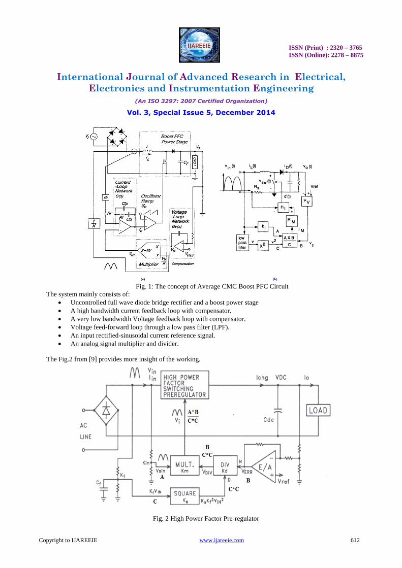
Fig. 1: The concept of Average CMC Boost PFC Circuit
The system mainly consists of:
Uncontrolled full wave diode bridge rectifier and a boost power stage
A high bandwidth current feedback loop with compensator.
A very low bandwidth Voltage feedback loop with compensator.
Voltage feed-forward loop through a low pass filter (LPF).
An input rectified-sinusoidal current reference signal.
An analog signal multiplier and divider.
The Fig.2 from [9] provides more insight of the working.
Fig. 2 High Power Factor Pre-regulator

ISSN (Print) : 2320 – 3765
ISSN (Online): 2278 – 8875
International Journal of Advanced Research in Electrical,
Electronics and Instrumentation Engineering
(An ISO 3297: 2007 Certified Organization)
Vol. 3, Special Issue 5, December 2014
Copyright to IJAREEIE www.ijareeie.com 613
A part of output voltage is compared with the reference to get an error signal (B), this is fed to the multiplier. A
signal (A), rectified sinusoidal signal is another input to the multiplier. These two signals can produce a rectified
sinusoidal control signal to the reference of current loop compensator, thus to obtain a unity PF i.e., sinusoidal input
current at input of the AC-DC converter.
In this context it can be noticed that when voltage and current are in phase power drawn is increased, and one of our
requirement being constant power is violated. The load can be either a resistor or a DC-DC converter. So in-order to
make power drawn independent of change in input RMS voltage a voltage feed-forward is utilised. The feed-forward
voltage is squared at the denominator and fed to the multiplier. A low pass filter in the way of feed-forward signal is to
step down the input voltage and to attenuate third harmonic ripple current in AC line from entering to the system, as
explained in [12].
The voltage loop is so slow that for the half sinusoid of input AC line, the divider output is a constant referring to
Fig.2. The output of the multiplier is then a rectified sinusoidal signal as reference to the current loop. This is like a
rectified-sinusoidal reference input to the controller a DC-DC converter, for which its output control signal should be
such that the output of the DC-DC converter should be a rectified-sinusoidal voltage. This is possible if the current loop
is a very fast acting one, having high bandwidth. In this case the output signal is the sensed average inductor current.
This makes current and voltage in phase, i.e. high PF. This fact is visible from Fig.1 (a). The Rs in Fig.1 (b) is the sense
resistor for sensing the average inductor current or the input current.
III. DESIGN SPECIFICATIONS
The design specification for the converter is the first step for design.
Input voltage = 230Vrms
Line frequency = 50Hz
Output voltage, Vo = 385VDC
Maximum output power, Pout = 250W
Switching frequency, fs = 100kHz
IV. POWER STAGE DESIGN
A. Boost Inductor
Peak current occur at min. Line Voltage, say 80Vrms. The duty cycle,
= 0.71.Peak current,
√
, of input sinusoid is 4.42A. Assuming inductor current ripple (ΔI = 900mA), Inductor (L) value is
chosen as 1mH from the inductor voltage slope equation at the turn-on time of switch. Inductance,
H (1)
B. Output Capacitor
The output capacitor serves a purpose of a filter, power source for a small period of time etc., the design criteria
includes:
Hold - up time, ΔT = 64mS
Decrease output voltage ripple
Decrease second harmonic ripple current
The output capacitor,
, is chosen as 470 μF . (2)

ISSN (Print) : 2320 – 3765
ISSN (Online): 2278 – 8875
International Journal of Advanced Research in Electrical,
Electronics and Instrumentation Engineering
(An ISO 3297: 2007 Certified Organization)
Vol. 3, Special Issue 5, December 2014
Copyright to IJAREEIE www.ijareeie.com 614
V. CONTROL BLOCK DIAGRAM OF ACMC BOOST PFC CONVERTER
The block diagram for the system is shown in Fig.3. The average CMC is an extension of peak CMC. The block
diagram and a very good explanation on peak CMC can be obtained from [4]. When the peak current ripple is very
small, peak CMC becomes equivalent to average CMC. Meanwhile, Average CMC includes a sensing resistor, current
loop compensator and does not require slope compensation when compared to peak CMC. The control block diagram
for average CMC can be obtained from [5]. The boost PFC circuit is an application of average CMC boost converter,
which includes a multiplier and divider as extra components. A mathematical mode for the multiplier-divider block can
be obtained from [11]. On combining [4, 5, 11], the following control block diagram is obtained.
Fig.3. Block Diagram of Average CMC Boost PFC Circuit
The Riis the sense resistor, Imp is the current controlling signal through Rm. D, Duty cycle, Ts, switching period, Vg is
the input voltage, Vo, the output voltage, Gvd(s), the control to output voltage transfer function, Gid(s) control to current
transfer function, Gvg(s), the voltage input to output transfer function, Gig(s), the current input to output transfer
function. Here, it is the output voltage and the inductor current, IL that is to be controlled. The block diagram is a
merger of mathematical modelling and physical appearance. This control block diagram is a must when dealing with
compensation of loops.
VI. INNER CURRENT CONTROL LOOP
A. Controller Design
The current loop is the inner loop and its open loop transfer function from Fig.3 is given by
, where, Gci(s) is current loop compensator, Fm
, where, Vs is the amplitude of the

ISSN (Print) : 2320 – 3765
ISSN (Online): 2278 – 8875
International Journal of Advanced Research in Electrical,
Electronics and Instrumentation Engineering
(An ISO 3297: 2007 Certified Organization)
Vol. 3, Special Issue 5, December 2014
Copyright to IJAREEIE www.ijareeie.com 615
triangular carrier for PWM generation. The PWM switch model when applied to boost converter [10], the small signal
equivalent circuit is as shown in Fig.4 (a).
Fig.4. Small Signal Model of Boost Power Stage (a)Exact, (b)Simplified
Since output capacitor large, capacitor can be thought of a constant voltage source. At high frequencies, capacitive
reactance is very low and can be modelled as short circuit Fig.4 (b). By circuit analysis, referring voltage source to 1°
side of the transformer, output inductor current to control transfer function,
(3)
1) Current Loop Compensation Strategy
The loop cross-over frequency is to be made16 kHz, and the Phase Margin is to be increased above 45° for
stable system. For this, a zero is added at 12 kHz and a pole is added at 128 kHz.
2) Current Loop Compensation Design
The actual down-slope (at turn-off period) of the inductor current becomes the up-slope at the non-inverting terminal
of the current loop compensator. Inductor current down-slope is given by (Vo - Vin)/L, and the worst case occurs when
Vin = 0, down-slope = Vo/L. The oscillator ramp slope = Vs*fs. The maximum gain the current compensator should
have is obtained by equating the amplified worst case down-slope sensed voltage to the oscillator ramp slope,[7] and is
given by Gca, and is found out to be 5.4 for peak to peak ramp voltage Vs=5.2V, sense resistor Ri=0.25 from
.
The uncompensated current loop gain is
.
For the current loop compensation, a PI controller is used. The figure Fig.5 shows a PI compensator. The gain 5.4 of
the compensator is set by ratio Rcz/Rci. And choosing Rcz = 20kΩ and Rci = 3.9kΩ is a good option. The loop transfer
function of PI compensator is given by, (
)
( ) (
)
(4)
ISSN (Print) : 2320 – 3765
ISSN (Online): 2278 – 8875
International Journal of Advanced Research in Electrical,
Electronics and Instrumentation Engineering
(An ISO 3297: 2007 Certified Organization)
Vol. 3, Special Issue 5, December 2014
Copyright to IJAREEIE www.ijareeie.com 616
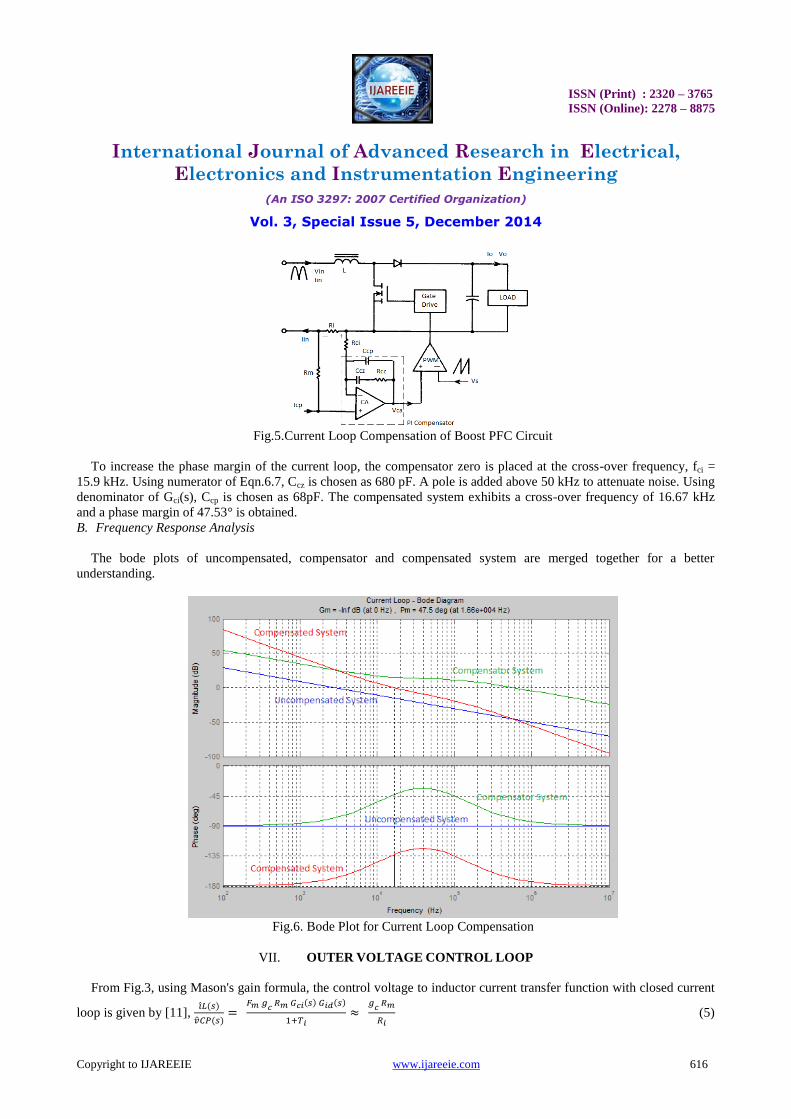
Fig.5.Current Loop Compensation of Boost PFC Circuit
To increase the phase margin of the current loop, the compensator zero is placed at the cross-over frequency, fci =
15.9 kHz. Using numerator of Eqn.6.7, Ccz is chosen as 680 pF. A pole is added above 50 kHz to attenuate noise. Using
denominator of Gci(s), Ccp is chosen as 68pF. The compensated system exhibits a cross-over frequency of 16.67 kHz
and a phase margin of 47.53° is obtained.
B. Frequency Response Analysis
The bode plots of uncompensated, compensator and compensated system are merged together for a better
understanding.
Fig.6. Bode Plot for Current Loop Compensation
VII. OUTER VOLTAGE CONTROL LOOP
From Fig.3, using Mason's gain formula, the control voltage to inductor current transfer function with closed current
loop is given by [11],
(5)

ISSN (Print) : 2320 – 3765
ISSN (Online): 2278 – 8875
International Journal of Advanced Research in Electrical,
Electronics and Instrumentation Engineering
(An ISO 3297: 2007 Certified Organization)
Vol. 3, Special Issue 5, December 2014
Copyright to IJAREEIE www.ijareeie.com 617
A. Voltage Loop Compensation for a Resistive Load (ΔVea=4)
Control voltage - Output voltage transfer function,
=
(6)
1) Compensation strategy
The compensator zero is placed at 2/RC and the compensator pole is added at 19 Hz. The cross-over frequency
obtained should be a maximum 19 Hz.
Since the system is of single pole, a PI controller is used for compensation.
Fig.7. PI Compensator for Voltage Loop
The loop transfer function of PI compensator is given by, (
)
( ) (
)
(7)
Rvi is chosen 511kΩ. Cvp is chosen such that to attenuate double frequency ripples. It is chosen such that to get a gain
of 0.0326 at double frequency, and is found out to be 47nF.As a strategy a zero is placed at 2/RC, ie, 1.19Hz. Cvz is
chosen as 754nF. A pole is added at at 19.1Hz.Rvz is chosen as 177kΩ.Rvdis chosen as 10kΩ to get a voltage of 7.5V
for a 385Voutput.
2) Frequency Response Analysis
Fig.8. Bode Plot of Voltage Loop – Resistive Load

ISSN (Print) : 2320 – 3765
ISSN (Online): 2278 – 8875
International Journal of Advanced Research in Electrical,
Electronics and Instrumentation Engineering
(An ISO 3297: 2007 Certified Organization)
Vol. 3, Special Issue 5, December 2014
Copyright to IJAREEIE www.ijareeie.com 618
B. Voltage Loop Compensation for a Constant Power Load (ΔVea=4, for PFC Chip UC3854[15])
Control voltage - Output voltage Transfer function,
=
(8)
1) Compensation strategy
Here, the compensator pole is added at 19 Hz. The cross-over frequency obtained should be a
maximum of
19 Hz.
A single pole is added for compensation.
Fig.9. PI Compensator for Voltage Loop – Constant Power Load
The loop transfer function of compensator is given by,
(
) (9)
All the components chosen are respectively the same as that of the resistive load case.
2) Frequency Response Analysis
Fig.10. Bode Plot of Voltage Loop – Constant Power Load
ISSN (Print) : 2320 – 3765
ISSN (Online): 2278 – 8875
International Journal of Advanced Research in Electrical,
Electronics and Instrumentation Engineering
(An ISO 3297: 2007 Certified Organization)
Vol. 3, Special Issue 5, December 2014
Copyright to IJAREEIE www.ijareeie.com 619
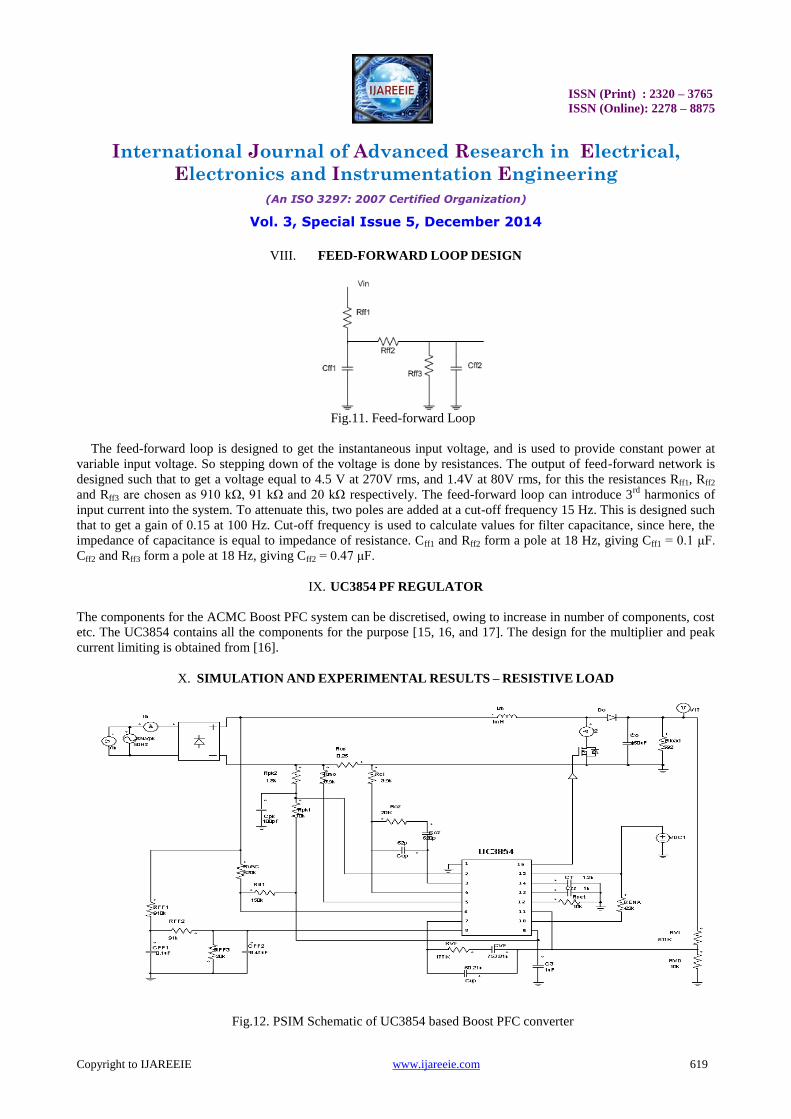
VIII. FEED-FORWARD LOOP DESIGN
Fig.11. Feed-forward Loop
The feed-forward loop is designed to get the instantaneous input voltage, and is used to provide constant power at
variable input voltage. So stepping down of the voltage is done by resistances. The output of feed-forward network is
designed such that to get a voltage equal to 4.5 V at 270V rms, and 1.4V at 80V rms, for this the resistances Rff1, Rff2
and Rff3 are chosen as 910 kΩ, 91 kΩ and 20 kΩ respectively. The feed-forward loop can introduce 3rd
harmonics of
input current into the system. To attenuate this, two poles are added at a cut-off frequency 15 Hz. This is designed such
that to get a gain of 0.15 at 100 Hz. Cut-off frequency is used to calculate values for filter capacitance, since here, the
impedance of capacitance is equal to impedance of resistance. Cff1 and Rff2 form a pole at 18 Hz, giving Cff1 = 0.1 μF.
Cff2 and Rff3 form a pole at 18 Hz, giving Cff2 = 0.47 μF.
IX. UC3854 PF REGULATOR
The components for the ACMC Boost PFC system can be discretised, owing to increase in number of components, cost
etc. The UC3854 contains all the components for the purpose [15, 16, and 17]. The design for the multiplier and peak
current limiting is obtained from [16].
X. SIMULATION AND EXPERIMENTAL RESULTS – RESISTIVE LOAD
Fig.12. PSIM Schematic of UC3854 based Boost PFC converter

ISSN (Print) : 2320 – 3765
ISSN (Online): 2278 – 8875
International Journal of Advanced Research in Electrical,
Electronics and Instrumentation Engineering
(An ISO 3297: 2007 Certified Organization)
Vol. 3, Special Issue 5, December 2014
Copyright to IJAREEIE www.ijareeie.com 620
Fig.13. Scaled Input Voltage and Current Fig.14.Output Voltage
Fig.15. Output Voltage at Step change of Load from 200 W (741 Ω) to 300 W (494 Ω)
XI. SIMULATION AND EXPERIMENTAL RESULTS – CONSTANT POWER LOAD
Fig.16. Buck Converter connected as Load for Boost PFC Circuit
200 W 300 W
ISSN (Print) : 2320 – 3765
ISSN (Online): 2278 – 8875
International Journal of Advanced Research in Electrical,
Electronics and Instrumentation Engineering
(An ISO 3297: 2007 Certified Organization)
Vol. 3, Special Issue 5, December 2014
Copyright to IJAREEIE www.ijareeie.com 621
A 385 V/50 V, 250 W, DC-DC closed loop buck converter was designed and simulated. Step reference and step
voltage tests where done for similar conditions as that with the resistor load.
Fig.17. Step Reference change from Vref= 2.683 V (200 W) Fig.18. Output Voltage at Step change of Load
from toVref = 3.28 V (300 W) 200 W (12.5 Ω) to 300 W (8.33 Ω)
XII. CONCLUSION
A 250 W, single phase PFC circuit based on ACMC boost converter was designed and simulated, with resistive load
and constant power load, using UC3854 PFC Chip. For a resistive load, 385V DC is obtained as output from 230Vrms
AC supply voltage and contains 120 Hz ripple. For a constant power load as buck converter, 50VDC is obtained at the
output with very less ripples, and can be loaded up to 5 A. It is observed that, as the loading of PFC circuit increase; the
input power factor is increased. Releasing the load degrades the power factor. This is observed in both resistive and
constant-power loads.
ACKNOWLEDGMENT
The authors wish to thank Dr. Mathews K. (Electronics and Communication Engineering Dept., Mar Athanasius
College of Engineering, Kothamangalam) and Prof. George John P. (Electrical and Electronics Dept., Mar Athanasius
College of Engineering, Kothamangalam)for his valuable opinions. Heartfelt thanks are extended to Mr.Nithin George
(P.G. Scholar, M. A. C. E) for his valuable points. Special thanks to Mr.Vinjohn Chirackal (P.G. Scholar, Kyungpook
National University, Republic of Korea).
REFERENCES
[1] Vlad Grigore, “Topological issues in single-phase power factor correction”, Doctor of Science in Technology dissertation, Dept. of Elect. And
Commun. Engg., Helsinki University of Technology, Finland, 2001.
[2] Muhammad H. Rashid, Power Electronics Handbook, 2nd edition, Academic Press, California.
[3] N. Mohan, T. M. Undeland, W. P. Robbins, Power Electronics: Converters, Applications, and Design. New York, NY, USA, John Wiley & Sons, Inc., 1995.
[4] Robert W. Erickson, Dragan Maksimović, Fundamentals of Power Electronics, 2nd Edition, Kluwer Academic Publishers, 2004, Boston.
[5] Philip Cooke, “Modeling average current mode control”, IEEE Proc., 2000, pp.256-262. [6] Wei Tang, Fred C. Le and Raymond B. Ridley, “Small-signal modeling of average current- mode control”, IEEE Trans. on Power Electronics,
pp. 112-118, Vol 8. No.2, April 1993.
[7] L. H. Dixon, ``Average current mode control of switching power supplies,``Unitrode Power Supply Design Seminar Manual, SEM-700, Unitrode Appl. Note U-140, 1990.
[8] R. B. Ridley, ``Average small-signal analysis of the boost power factor correction circuit", VPEC Seminar Proceedings, 1989, pp. 108-120.
[9] L. H. Dixon, ``High power factor pre-regulator for off-line power supplies," Unitrode Power Supply Design Seminar Manual, SEM-600, 1988.
[10] Chen Zhou, Milan M. Jovanović, ``Design trade-offs in continuous current-mode controlled boost power-factor correction circuits", High
Frequency Power Conversion Conference, May 1992, pp. 209-219.
[11] Fakhralden A. Huliel, Fred C. Lee and Bo H. Cho, ``Small-signal modelling of the single-phase boost high power factor converter with constant frequency control", Conf .Record, Power Electronics Specialists Conference, 1992, pp. 475-482.
[12] Alexander Abramovitch and Sam Ben-Yaakov, ``Analysis and design of feedback and feed-forward paths of active power factor correction
systems for minimum input current distortion", Conf. Record, IEEE Power Electronics Specialists Conference, 1995, pp. 1009-1014.
200 W
300 W
200 W
300 W

ISSN (Print) : 2320 – 3765
ISSN (Online): 2278 – 8875
International Journal of Advanced Research in Electrical,
Electronics and Instrumentation Engineering
(An ISO 3297: 2007 Certified Organization)
Vol. 3, Special Issue 5, December 2014
Copyright to IJAREEIE www.ijareeie.com 622
[13] L. H. Dixon, ``High power factor switching pre-regulator design optimization," Unitrode Power Supply Design Seminar Manual, SEM-700,
1990.
[14] J. P. Noon, D. Dalal, ``Practical design issues for PFC circuits," in Proc. IEEE Applied Power Electronics Conference, 1997, pp. 51-58. [15] Unitrode, ``High Power Factor Preregulator,"UC3854 Data-sheet, Texas Instruments Incorporated, 2012.
[16] Philip. C. Todd, ``UC3854 controlled power factor correction circuit design, ``Unitrode Appl. Note U-134 Unitrode Corporation, Merrimack,
NH, 1999.
[17] B.Andreycak, ``Optimizing Performance in UC3854 power factor correction application", Unitrode Appl. Note DN-39E, Unitrode products
and application handbook, 1993/94. [18] Amir M. Rahimi, Parviz Parto, and Peyman Asadi, Compensator Design Procedure for Buck Converter with Voltage-Mode Error-Amplifier,
Application Note AN-1162, International Rectifier.
[19] Blessen Antony Francis, Dr. Bos Mathew Jos, ``Design and implementation of a 12 V/ 6V, 3WClosed Loop Synchronous DC-DC Buck Converter in Continuous Conduction Mode”, Mar Athanasius College of Engineering, Kothamangalam, March 2014, Unpublished.
BIOGRAPHY
Blessen AntonyFrancis received B.Tech Degree in Electrical and Electronics Engineering from
Rajagiri School of Engineering and Technology, Kochi, Kerala, India in 2011. He is pursuing the
M.Tech Degree in Power Electronics in Mar Athanasius College of Engineering, Kothamangalam,
Kerala, affiliated to Mahatma Gandhi University, Kottayam. His areas of interest include Power
Converters, Analog Control Systems and Power Factor Correction Techniques.
Bos Mathew Jos received B.Tech Degree in Electrical and Electronics Engineering from Mahatma
Gandhi University, Kottayam in 1993, M.Tech Degree and Ph.D. in Power Electronics from National
Institute of Technology, Trichy in 2004 and 2010 respectively. He is currently working as an
Associate Professor in Mar Athanasius College of Engineering, Kothamangalam, and Kerala with a
teaching experience of 16 years. He has presented several papers in different National and
International conferences and is a life member of ISTE. His areas of interest include Power
Electronics, Electric Drives and Controls and Electrical Machines.