voodoo 2 graphics h p e 3d g a - sourceforgedarwin-3dfx.sourceforge.net/voodoo2.pdf · voodoo 2...
TRANSCRIPT

Proprietary Information
VOODOO2 GRAPHICS
HIGH PERFORMANCE GRAPHICS ENGINE
FOR 3D GAME ACCELERATION
Revision 1.16
December1, 1999 Copyright 1996-1999 3Dfx Interactive, Inc. All Rights Reserved
3Dfx Interactive, Inc.
4435 Fortran Drive San Jose, CA 95134
Phone: (408) 935-4400 Fax: (408) 262-8602
www.3dfx.com
Voodoo2 Graphics
Copyright 1996-1998 3Dfx Interactive, Inc. Revision 1.16 Proprietary 2 Updated 12/1/99
Copyright Notice: [English translations from legalese in brackets] ©1996-1999, 3Dfx Interactive, Inc. All rights reserved This document may be reproduced in written, electronic or any other form of expression only in its entirety. [If you want to give someone a copy, you are hereby bound to give him or her a complete copy.] This document may not be reproduced in any manner whatsoever for profit. [If you want to copy this document, you must not charge for the copies other than a modest amount sufficient to cover the cost of the copy.]
No Warranty THESE SPECIFICATIONS ARE PROVIDED BY 3DFX "AS IS" WITHOUT ANY REPRESENTATION OR WARRANTY, EXPRESS OR IMPLIED, INCLUDING ANY WARRANTY OF MERCHANTABILITY, FITNESS FOR A PARTICULAR PURPOSE, NONINFRINGEMENT OF THIRD-PARTY INTELLECTUAL PROPERTY RIGHTS, OR ARISING FROM THE COURSE OF DEALING BETWEEN THE PARTIES OR USAGE OF TRADE. IN NO EVENT SHALL 3DFX BE LIABLE FOR ANY DAMAGES WHATSOEVER INCLUDING, WITHOUT LIMITATION, DIRECT OR INDIRECT DAMAGES, DAMAGES FOR LOSS OF PROFITS, BUSINESS INTERRUPTION, OR LOSS OF INFORMATION) ARISING OUT OF THE USE OF OR INABILITY TO USE THE SPECIFICATIONS, EVEN IF 3DFX HAS BEEN ADVISED OF THE POSSIBILITY OF SUCH DAMAGES. [You're getting it for free. We believe the information provided to be accurate. Beyond that, you're on your own.]

Voodoo2 Graphics
Copyright 1996-1998 3Dfx Interactive, Inc. Revision 1.16 Proprietary 3 Updated 12/1/99
COPYRIGHT NOTICE: ..................................................................................................................................... 2
NO WARRANTY ....................................................................................................................................................... 2
1. GENERAL DESCRIPTION ........................................................................................................................ 7
2. PERFORMANCE......................................................................................................................................... 9
3. ARCHITECTURAL AND FUNCTIONAL OVERVIEW..........................................................................11
3.1 SYSTEM LEVEL DIAGRAMS..........................................................................................................................11 3.2 ARCHITECTURAL OVERVIEW ...................................................................................................................... 14 3.3 FUNCTIONAL OVERVIEW ............................................................................................................................ 15
4. VOODOO2 GRAPHICS ADDRESS SPACE............................................................................................. 20
5. MEMORY MAPPED REGISTER SET .................................................................................................... 21
5.1 STATUS REGISTER....................................................................................................................................... 29 5.2 INTRCTRL REGISTER.................................................................................................................................. 30 5.3 VERTEX AND FVERTEX REGISTERS ............................................................................................................... 31 5.4 STARTR, STARTG, STARTB, STARTA, FSTARTR, FSTARTG, FSTARTB, AND FSTARTA REGISTERS....................... 31 5.5 STARTZ AND FSTARTZ REGISTERS ............................................................................................................... 32 5.6 STARTS, STARTT, FSTARTS, AND FSTARTT REGISTERS.................................................................................. 32 5.7 STARTW AND FSTARTW REGISTERS............................................................................................................. 33 5.8 DRDX, DGDX, DBDX, DADX, FDRDX, FDGDX, FDBDX, AND FDADX REGISTERS ...................................... 33 5.9 DZDX AND FDZDX REGISTERS................................................................................................................... 33 5.10 DSDX, DTDX, FDSDX, AND FDTDX REGISTERS.......................................................................................... 34 5.11 DWDX AND FDWDX REGISTERS ................................................................................................................ 34 5.12 DRDY, DGDY, DBDY, DADY, FDRDY, FDGDY, FDBDY, AND FDADY REGISTERS ......................................... 34 5.13 DZDY AND FDZDY REGISTERS................................................................................................................... 35 5.14 DSDY, DTDY, FDSDY, AND FDTDY REGISTERS ........................................................................................... 35 5.15 DWDY AND FDWDY REGISTERS ................................................................................................................ 35 5.16 TRIANGLECMD AND FTRIANGLECMD REGISTERS ...................................................................................... 36 5.17 FBZCOLORPATH REGISTER ......................................................................................................................... 36 5.18 FOGMODE REGISTER.................................................................................................................................. 41 5.19 ALPHAMODE REGISTER.............................................................................................................................. 43
5.19.1 Alpha function .................................................................................................................................. 44 5.19.2 Alpha Blending ................................................................................................................................. 45
5.20 FBZMODE REGISTER .................................................................................................................................. 46 5.20.1 Depth-buffering function................................................................................................................... 50
5.21 LFBMODE REGISTER .................................................................................................................................. 50 5.21.1 Linear Frame Buffer Writes............................................................................................................... 53 5.21.2 Linear Frame Buffer Reads ............................................................................................................... 56
5.22 CLIPLEFTRIGHT AND CLIPLOWYHIGHY REGISTERS .................................................................................... 57 5.23 NOPCMD REGISTER .................................................................................................................................. 58 5.24 FASTFILLCMD REGISTER ........................................................................................................................... 58 5.25 SWAPBUFFERCMD REGISTER ..................................................................................................................... 59 5.26 FOGCOLOR REGISTER ................................................................................................................................ 59 5.27 ZACOLOR REGISTER................................................................................................................................... 60 5.28 CHROMAKEY REGISTER ............................................................................................................................. 60
Voodoo2 Graphics
Copyright 1996-1998 3Dfx Interactive, Inc. Revision 1.16 Proprietary 4 Updated 12/1/99
5.29 CHROMARANGE REGISTER ......................................................................................................................... 60 5.30 USERINTRCMD REGISTER ......................................................................................................................... 61 5.31 STIPPLE REGISTER...................................................................................................................................... 62 5.32 COLOR0 REGISTER..................................................................................................................................... 62 5.33 COLOR1 REGISTER..................................................................................................................................... 62 5.34 FBITRIANGLESOUT REGISTER..................................................................................................................... 62 5.35 FBIPIXELSIN REGISTER............................................................................................................................... 63 5.36 FBICHROMAFAIL REGISTER ........................................................................................................................ 63 5.37 FBIZFUNCFAIL REGISTER............................................................................................................................ 63 5.38 FBIAFUNCFAIL REGISTER ........................................................................................................................... 63 5.39 FBIPIXELSOUT REGISTER ........................................................................................................................... 63 5.40 FBISWAPHISTORY REGISTER ....................................................................................................................... 64 5.41 FOGTABLE REGISTER ................................................................................................................................. 64 5.42 VRETRACE REGISTER ................................................................................................................................. 65 5.43 HVRETRACE REGISTER............................................................................................................................... 65 5.44 HSYNC REGISTER....................................................................................................................................... 66 5.45 VSYNC REGISTER....................................................................................................................................... 66 5.46 BACKPORCH REGISTER............................................................................................................................... 66 5.47 VIDEODIMENSIONS REGISTER ..................................................................................................................... 66 5.48 MAXRGBDELTA REGISTER .......................................................................................................................... 66 5.49 HBORDER REGISTER .................................................................................................................................. 67 5.50 VBORDER REGISTER .................................................................................................................................. 67 5.51 BORDERCOLOR REGISTER .......................................................................................................................... 67 5.52 FBIINIT0 REGISTER .................................................................................................................................... 67 5.53 FBIINIT1 REGISTER .................................................................................................................................... 68 5.54 FBIINIT2 REGISTER .................................................................................................................................... 69 5.55 FBIINIT3 REGISTER .................................................................................................................................... 70 5.56 FBIINIT4 REGISTER .................................................................................................................................... 70 5.57 FBIINIT5 REGISTER .................................................................................................................................... 71 5.58 FBIINIT6 REGISTER .................................................................................................................................... 72 5.59 FBIINIT7 REGISTER .................................................................................................................................... 73 5.60 CMDFIFOBASEADDR REGISTER .................................................................................................................. 74 5.61 CMDFIFOBUMP REGISTER........................................................................................................................... 74 5.62 CMDFIFORDPTR REGISTER......................................................................................................................... 74 5.63 CMDFIFOAMIN REGISTER .......................................................................................................................... 74 5.64 CMDFIFOAMAX REGISTER ......................................................................................................................... 74 5.65 CMDFIFODEPTH REGISTER ......................................................................................................................... 74 5.66 CMDFIFOHOLES REGISTER ......................................................................................................................... 75 5.67 CLUTDATA REGISTER ................................................................................................................................. 75 5.68 DACDATA REGISTER................................................................................................................................... 75 5.69 SSETUPMODE REGISTER ............................................................................................................................ 76 5.70 TRIANGLE SETUP VERTEX REGISTERS ......................................................................................................... 76 5.71 SARGB REGISTER ..................................................................................................................................... 77 5.72 SWB REGISTER .......................................................................................................................................... 77 5.73 SS/W0 REGISTER....................................................................................................................................... 78 5.74 ST/W0 REGISTER ...................................................................................................................................... 78 5.75 SVZ REGISTER ........................................................................................................................................... 78 5.76 SWTMU0 REGISTER ................................................................................................................................... 78 5.77 SWTMU1 REGISTER ................................................................................................................................... 78 5.78 SS/WTMU1 REGISTER ................................................................................................................................ 78
Voodoo2 Graphics
Copyright 1996-1998 3Dfx Interactive, Inc. Revision 1.16 Proprietary 5 Updated 12/1/99
5.79 ST/WTMU1 REGISTER................................................................................................................................ 78 5.80 SALPHA REGISTER ..................................................................................................................................... 78 5.81 SRED REGISTER ......................................................................................................................................... 79 5.82 SGREEN REGISTER ..................................................................................................................................... 79 5.83 SBLUE REGISTER ....................................................................................................................................... 79 5.84 SDRAWTRICMD REGISTER ........................................................................................................................ 79 5.85 SBEGINTRICMD REGISTER........................................................................................................................ 79 5.86 TEXTUREMODE REGISTER .......................................................................................................................... 79 5.87 TLOD REGISTER ....................................................................................................................................... 82 5.88 TDETAIL REGISTER .................................................................................................................................... 84 5.89 TEXBASEADDR, TEXBASEADDR1, TEXBASEADDR2, AND TEXBASEADDR38 REGISTERS............................... 85 5.90 TREXINIT0 REGISTER................................................................................................................................. 85 5.91 TREXINIT1 REGISTER................................................................................................................................. 85 5.92 NCCTABLE0 AND NCCTABLE1/PALETTE REGISTERS ..................................................................................... 85
5.92.1 NCC Table ........................................................................................................................................ 85 5.92.2 8-Bit Palette...................................................................................................................................... 86
5.93 BLTCOMMAND REGISTER ........................................................................................................................... 87 5.94 BLTSRCBASEADDR .................................................................................................................................... 91 5.95 BLTDSTBASEADDR .................................................................................................................................... 91 5.96 BLTXYSTRIDES ......................................................................................................................................... 92 5.97 BLTSRCCHROMARANGE............................................................................................................................. 93 5.98 BLTDSTCHROMARANGE............................................................................................................................. 94 5.99 BLTCLIPX AND BLTCLIPY .......................................................................................................................... 94 5.100 BLTSRCXY............................................................................................................................................ 95 5.101 BLTDSTXY............................................................................................................................................ 95 5.102 BLTSIZE................................................................................................................................................. 96 5.103 BLTROP ................................................................................................................................................. 97 5.104 BLTCOLOR............................................................................................................................................. 98 5.105 BLTDATA ............................................................................................................................................... 99
6. PCI CONFIGURATION REGISTER SET ..............................................................................................102
6.1 VENDOR_ID REGISTER .............................................................................................................................102 6.2 DEVICE_ID REGISTER...............................................................................................................................102 6.3 COMMAND REGISTER................................................................................................................................102 6.4 STATUS REGISTER .....................................................................................................................................103 6.5 REVISION_ID REGISTER............................................................................................................................103 6.6 CLASS_CODE REGISTER ............................................................................................................................104 6.7 CACHE_LINE_SIZE REGISTER.....................................................................................................................104 6.8 LATENCY_TIMER REGISTER.......................................................................................................................104 6.9 HEADER_TYPE REGISTER ..........................................................................................................................104 6.10 BIST REGISTER........................................................................................................................................104 6.11 MEMBASEADDR REGISTER ........................................................................................................................104 6.12 INTERRUPT_LINE REGISTER.......................................................................................................................105 6.13 INTERRUPT_PIN REGISTER.........................................................................................................................105 6.14 MIN_GNT REGISTER .................................................................................................................................105 6.15 MAX_LAT REGISTER .................................................................................................................................105 6.16 INITENABLE REGISTER..............................................................................................................................106 6.17 BUSSNOOP0 AND BUSSNOOP1 REGISTERS ..................................................................................................107 6.18 CFGSTATUS REGISTER ...............................................................................................................................107 6.19 CFGSCRATCH REGISTER ............................................................................................................................107
Voodoo2 Graphics
Copyright 1996-1998 3Dfx Interactive, Inc. Revision 1.16 Proprietary 6 Updated 12/1/99
6.20 SIPROCESS REGISTER ................................................................................................................................107
7. 3D COMMAND DESCRIPTIONS ...........................................................................................................108
7.1 NOP COMMAND.......................................................................................................................................108 7.2 TRIANGLE COMMAND ...........................................................................................................................108 7.3 FASTFILL COMMAND .............................................................................................................................108 7.4 SWAPBUFFER COMMAND ......................................................................................................................108 7.5 USERINTERRUPT COMMAND ................................................................................................................109
8. 2D COMMAND DESCRIPTIONS ...........................................................................................................110
8.1 SCREEN-TO-SCREEN BITBLT COMMAND....................................................................................................111 8.2 CPU-TO-SCREEN BITBLT COMMAND ........................................................................................................112 8.3 BITBLT RECTANGLE FILL COMMAND.........................................................................................................112 8.4 SGRAM FILL COMMAND ..........................................................................................................................112 8.5 REGISTER USE BY COMMAND ....................................................................................................................113 8.6 COMMAND USE BY REGISTER.....................................................................................................................113
9. LINEAR FRAME BUFFER ACCESS......................................................................................................114
9.1 LINEAR FRAME BUFFER WRITES .................................................................................................................114 9.2 LINEAR FRAME BUFFER READS...................................................................................................................115
10. TEXTURE MEMORY ACCESS ..........................................................................................................116
11. CMDFIFO OPERATION......................................................................................................................120
11.1 LEGACY ADDRESS MAP ............................................................................................................................120 11.2 CMDFIFO ADDRESS MAP ........................................................................................................................121 11.3 COMMAND TRANSPORT.............................................................................................................................122
11.3.1 CMDFIFO Management ..................................................................................................................122 11.3.2 CMDFIFO Data...............................................................................................................................123 11.3.3 CMDFIFO Packet Type 0.................................................................................................................123 11.3.4 CMDFIFO Packet Type 1.................................................................................................................124 11.3.5 CMDFIFO Packet Type 2.................................................................................................................124 11.3.6 CMDFIFO Packet Type 3.................................................................................................................125 11.3.7 CMDFIFO Packet Type 4.................................................................................................................126 11.3.8 CMDFIFO Packet Type 5.................................................................................................................127
12. PROGRAMMING CAVEATS ..............................................................................................................128
12.1 I/O ACCESSES ..........................................................................................................................................128 12.2 MEMORY ACCESSES..................................................................................................................................128 12.3 DETERMINING CVG IDLE CONDITION .......................................................................................................128 12.4 TRIANGLE SUBPIXEL CORRECTION ............................................................................................................128 12.5 LOADING THE INTERNAL COLOR LOOKUP TABLE ........................................................................................129
13. VIDEO TIMING ...................................................................................................................................130
14. REVISION HISTORY...........................................................................................................................132

Voodoo2 Graphics
Copyright 1996-1998 3Dfx Interactive, Inc. Revision 1.16 Proprietary 7 Updated 12/1/99
1. General Description Important Note: Throughout this document, features, descriptions, and specifications which are marked with the * symbol are not present in the Alpha version of the Voodoo2 Graphics chipset. Voodoo2 Graphics from 3Dfx Interactive is a second generation 3D graphics accelerator specifically designed to address the requirements of the game console, location-based entertainment, arcade, and PC game enthusiast markets. Optimized for real-time texture-mapped 3D applications, Voodoo2 Graphics provides acceleration for advanced 3D features including true-perspective texture mapping with trilinear mipmapping and lighting, detail and projected texture mapping, texture and polygonal anti-aliasing, and high precision sub-pixel correction. Voodoo2 Graphics also supports general purpose 3D pixel processing functions including polygonal-based Gouraud shading, depth-buffering, alpha blending, and dithering. In addition, Voodoo2 Graphics includes an optimized 2D BitBLT engine to accelerate traditional Windows GDI primitives.
3D Features • Triangle raster engine • Full hardware triangle setup supporting backface culling in addition to triangle primitives
independent, strips, and fans • Sub-pixel correction to .4 x .4 resolution • Polygonal anti-aliasing* • Linearly interpolated Gouraud-shaded rendering • Perspective-corrected (divide-per-pixel) texture-mapped rendering with iterated RGB
modulation/addition/blending • Texture filtering: point-sampling, bilinear, and trilinear filtering • Per-pixel Mipmapping with programmable Mipmap LOD bias and clamping • Detail and Projected Texture mapping • 16-bit texture formats: RGB(5-6-5), ARGB(8-3-3-2), ARGB(1-5-5-5), ARGB(4-4-4-4), Alpha-
Intensity(8-8), Alpha-Palette (8-8 expanded to RGB 8-8-8), and AYAB(8-4-2-2) • 8-bit texture formats: RGB(3-3-2), YAB(4-2-2), Alpha(8), Intensity(8), Alpha-Intensity(4-4),
PalettedRGB(8 expanded to RGB 8-8-8) and PalettedARGB(8 expanded to ARGB 6-6-6-6)* • Texture decompression: 8-bit “narrow channel” YAB • Embedded 512-entry texture palette with command to automatically load palette from texture memory
(256-entry texture palette in Alpha version) • Texture coordinate clamping, wrapping, and mirroring (mirroring not present in Alpha version) • Linearly interpolated 16-bit Z-buffer rendering • Perspective-corrected 16-bit floating point W-buffer rendering • 8 depth comparison functions • Programmable depth biasing and depth stenciling • Transparency with dedicated color mask and chroma-keying • Source/Destination pixel alpha blending • 8 alpha comparison functions • Per-pixel fog using interpolated fog lookup table and programmable color • 24-bit color dithering to native 16-bit RGB buffer using 4x4 or 2x2 ordered dither matrix
2D Features • Direct memory-mapped access to frame buffer and texture memories via linear address mapping • 2D BitBLT engine supporting CPU-to-Screen and Screen-to-Screen transfers • Separate programmable strides for Source and Destination areas during BitBLT transfers
Voodoo2 Graphics
Copyright 1996-1998 3Dfx Interactive, Inc. Revision 1.16 Proprietary 8 Updated 12/1/99
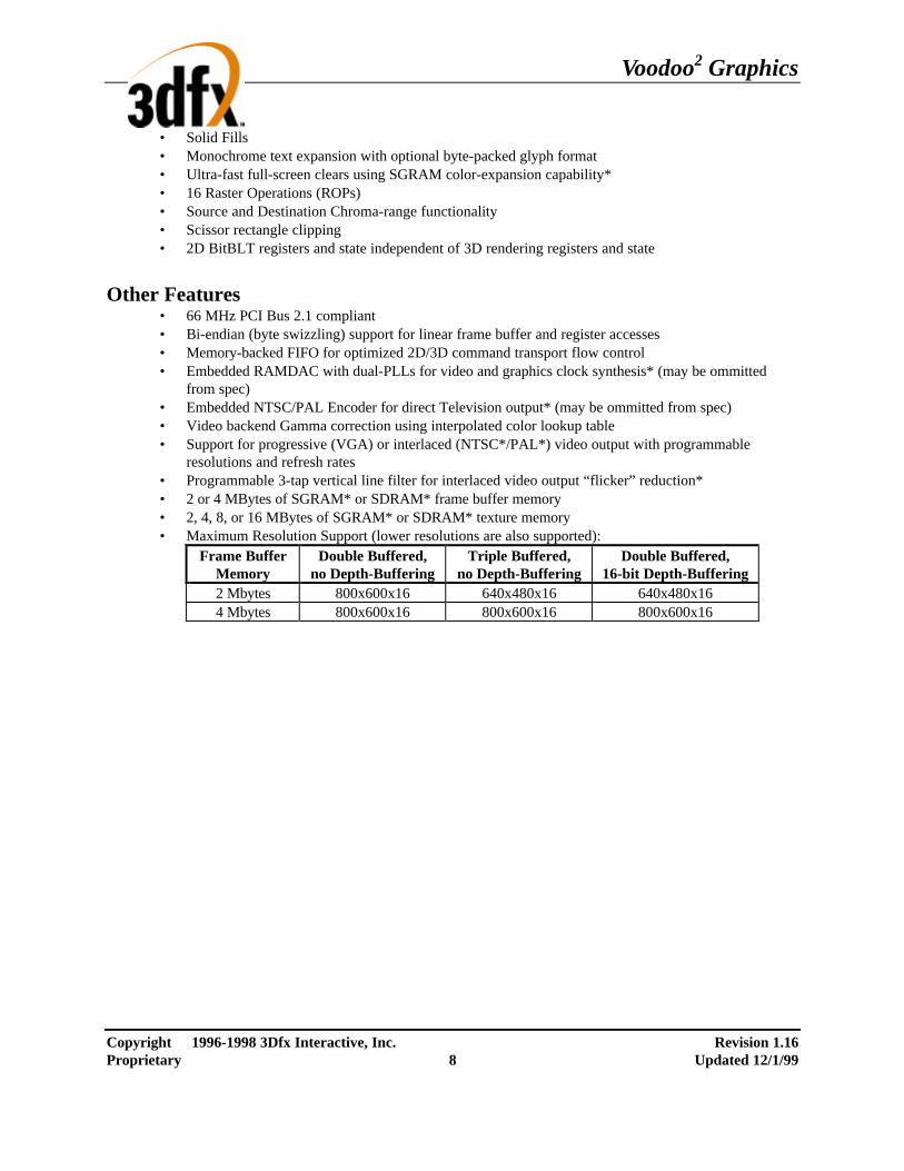
• Solid Fills • Monochrome text expansion with optional byte-packed glyph format • Ultra-fast full-screen clears using SGRAM color-expansion capability* • 16 Raster Operations (ROPs) • Source and Destination Chroma-range functionality • Scissor rectangle clipping • 2D BitBLT registers and state independent of 3D rendering registers and state
Other Features
• 66 MHz PCI Bus 2.1 compliant • Bi-endian (byte swizzling) support for linear frame buffer and register accesses • Memory-backed FIFO for optimized 2D/3D command transport flow control • Embedded RAMDAC with dual-PLLs for video and graphics clock synthesis* (may be ommitted
from spec) • Embedded NTSC/PAL Encoder for direct Television output* (may be ommitted from spec) • Video backend Gamma correction using interpolated color lookup table • Support for progressive (VGA) or interlaced (NTSC*/PAL*) video output with programmable
resolutions and refresh rates • Programmable 3-tap vertical line filter for interlaced video output “flicker” reduction* • 2 or 4 MBytes of SGRAM* or SDRAM* frame buffer memory • 2, 4, 8, or 16 MBytes of SGRAM* or SDRAM* texture memory • Maximum Resolution Support (lower resolutions are also supported):
Frame Buffer Memory
Double Buffered, no Depth-Buffering
Triple Buffered, no Depth-Buffering
Double Buffered, 16-bit Depth-Buffering
2 Mbytes 800x600x16 640x480x16 640x480x16 4 Mbytes 800x600x16 800x600x16 800x600x16

Voodoo2 Graphics
Copyright 1996-1998 3Dfx Interactive, Inc. Revision 1.16 Proprietary 9 Updated 12/1/99
2. Performance The following table shows the peak performance of Voodoo2 Graphics. Note that the numbers included illustrate the maximum performance and number of pixels per clock generated for particular operations. The numbers below should not be used to estimate real-world performance, as Monitor/TV refresh, DRAM refresh, rendering DRAM page misses, and memory FIFO operation lowers overall performance. The numbers below assume a 75 MHz graphics clock frequency.
Operation / Command Peak Pixels per Clock Generated Peak Fill Rate Generated Rendered Triangles / TRIANGLE command
1 75 MPixels/sec
Solid Fills / FASTFILL command 2 150 MPixels/sec Solid Fills / BITBLT command 1 75 MPixels/sec CPU-to-Screen BLT / BITBLT command 1 75 MPixels/sec Screen-to-Screen BLT / BITBLT command .5 37 MPixels/sec Ultra-fast clears using SGRAM color-expand / BITBLT command
16* (4 for Alpha version) 1200 MPixels/sec* (300 MPixels/sec for alpha version)
The tables below show more realistic, real-world estimated performance of Voodoo2 Graphics. Performance is calculated assuming that the PCI Bus master is supplying data at its peak bandwidth. Thus, the performance levels are the maximum sustainable rates of Voodoo2 Graphics, not necessarily the system performance. If a particular operation is CPU limited or a particular PCI bus master is not supplying data at its peak rate, then the effective system performance level will decrease. All numbers are estimated assuming 16-bit frame buffer pixels, the memory-backed FIFO disabled, 640x480 resolution @ 60 Hz refresh rate, and a 75 MHz graphics clock frequency driving SGRAMs. The estimated triangle performance numbers assume all triangles are rendered and not backface culled by the triangle setup engine. Single color, rendered triangles (no hardware triangle setup, Gouraud shading, fogging, alpha-blending, Z-buffering, or sub-pixel correction)
Ktriangles/sec
10-pixel, right-angled, horizontally oriented 25-pixel, right-angled, horizontally oriented 50-pixel, right-angled, horizontally oriented 1000-pixel, right-angled, horizontally oriented Hardware setup, RGB Gouraud shaded, per-pixel fogged, alpha-blended, Z-buffered, sub-pixel corrected, rendered triangles
Ktriangles/sec
10-pixel, right-angled, randomly oriented 25-pixel, right-angled, randomly oriented 50-pixel, right-angled, randomly oriented 1000-pixel, right-angled, randomly oriented Hardware setup, bilinear filtered, Mipmapped, texture-mapped, RGB Gouraud shaded, per-pixel fogged, sub-pixel corrected, rendered triangles (no alpha-blending or Z-buffering)
Ktriangles/sec
10-pixel, right-angled, randomly oriented 25-pixel, right-angled, randomly oriented 50-pixel, right-angled, randomly oriented 1000-pixel, right-angled, randomly oriented

Voodoo2 Graphics
Copyright 1996-1998 3Dfx Interactive, Inc. Revision 1.16 Proprietary 10 Updated 12/1/99
Hardware setup, bilinear filtered, Mipmapped, , texture-mapped, RGB Gouraud shaded, per-pixel fogged, alpha-blended, Z-buffered, sub-pixel corrected, rendered triangles
Ktriangles/sec
10-pixel, right-angled, randomly oriented 25-pixel, right-angled, randomly oriented 50-pixel, right-angled, randomly oriented 1000-pixel, right-angled, randomly oriented Full-Screen Clears (using FASTFILL command) msec RGB Buffer Depth Buffer RBG and Depth Buffer simultaneously Full-Screen Clears (using SGRAM ColorExpand BITBLT command) msec RGB Buffer Depth Buffer RBG and Depth Buffer simultaneously

Voodoo2 Graphics
Copyright 1996-1998 3Dfx Interactive, Inc. Revision 1.16 Proprietary 11 Updated 12/1/99
3. Architectural and Functional Overview
3.1 System Level Diagrams In its entry level configuration, a Voodoo2 Graphics graphics solution consists of two rendering ASICS: Chuck and Bruce. Chuck serves as a PCI slave device, and all communication from the host CPU to Voodoo2 Graphics is performed through Chuck. Chuck implements 3D features including triangle setup, Gouraud shading, alpha blending, fogging, depth-buffering, and dithering. Chuck also includes logic for the 2D BitBLT engine, and processes all linear frame buffer accesses. Additionally, Chuck includes a video display controller which controls output to the display monitor or Television. Bruce implements all of the texture mapping capabilities of Voodoo2 Graphics. Bruce includes logic to support true-perspective texture mapping (dividing by W every pixel), level-of-detail (LOD) mipmapping, and bilinear filtering. Additionally, Bruce implements advanced texture mapping techniques such as detail texture mapping, projected texture mapping, and trilinear texture filtering. Both Chuck and Bruce support both SGRAM and SDRAM to provide a wide range of price/performance options. Note in the single Bruce Voodoo2 Graphics solution, the advanced texture mapping techniques of detail texture mapping, projected texture mapping, and trilinear texture filtering are two-pass operations. There is no performance penalty, however, for point-sampled or bilinear filtered texture mapping with mipmapping with the single Bruce solution. The diagram below illustrates a base-level Voodoo2 Graphics graphics solution.
PCI System Bus
ChuckFrameBuffer
Interface
FrameBuffer
Memory
monitor
BruceTexture MappingEngine
TextureMemory
no connect
2-4 MBytes SDRAM/SGRAM
2-16 MBytes SDRAM/SGRAM
TV
Bruce includes a dedicated expansion bus which allows either an external device to directly access texture memory or for multiple Bruce ASICs to be chained together for improved performance and functionality. Bruce reads the value of a strapping pin upon power-up reset to determine whether the expansion bus is to be used as a direct port to texture memory (“DT Bus”) or as a way of chaining multiple Bruce ASICs together (“TT Bus”). The diagram below shows the Bruce expansion bus configured as a DT Bus* (DT Bus is not included in the Alpha version):

Voodoo2 Graphics
Copyright 1996-1998 3Dfx Interactive, Inc. Revision 1.16 Proprietary 12 Updated 12/1/99
PCI System Bus(66 MHz) Chuck
FrameBuffer
Interface
FrameBuffer
Memory
monitor
BruceTexture MappingEngine
TextureMemoryDT Bus
(75 MHz)
2-4 MBytesSDRAM/SGRAM
(75 MHz)
2-16 MBytesSDRAM/SGRAM
(75 MHz)
TV
CPUSystemASIC
SystemMemory
4-16 MBytesSDRAM/SGRAM
(100 MHz)
By configuring the Bruce expansion bus as a way of chaining together multiple Bruce ASICs, the performance of advanced texture mapping features such as detailed texture mapping, projected texture mapping, and trilinear filtering can be doubled. A two Bruce Voodoo2 Graphics graphics solution allows single pass, full-speed, detail texture mapping, projected texture mapping, or trilinear filtering. The diagram below illustrates a two Bruce graphics solution:
PCI System Bus
ChuckFrameBuffer
Interface
FrameBuffer
Memory
BruceTexture MappingEngine
TextureMemory
BruceTexture MappingEngine
TextureMemory
no connect
2-4 MBytes SDRAM/SGRAM
2-16 MBytes SDRAM/SGRAM
2-16 MBytes SDRAM/SGRAM
monitor TV
Three Bruce ASICs can also be chained together to provide single-pass, full-speed rendering of all supported advanced texture mapping features including projected texture mapping. The diagram below illustrates the three Bruce Voodoo2 Graphics graphics architecture:
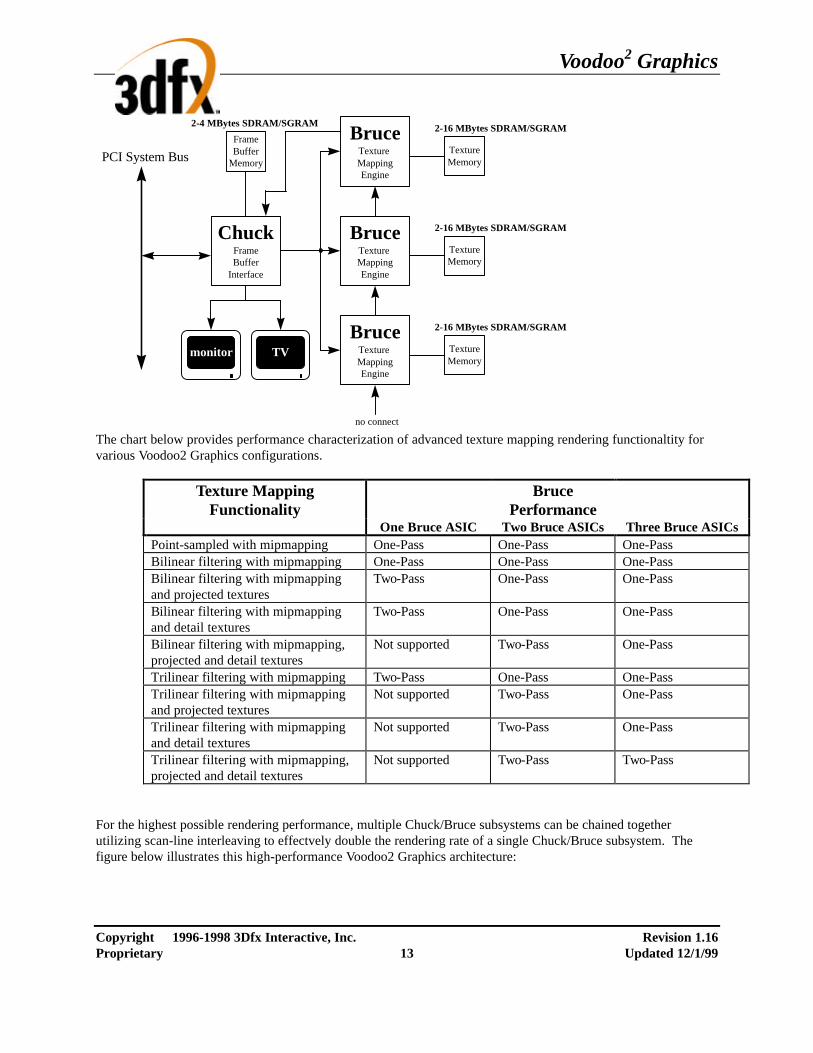
Voodoo2 Graphics
Copyright 1996-1998 3Dfx Interactive, Inc. Revision 1.16 Proprietary 13 Updated 12/1/99
ChuckFrameBuffer
Interface
FrameBuffer
Memory
BruceTexture MappingEngine
TextureMemory
BruceTexture MappingEngine
TextureMemory
BruceTexture MappingEngine
TextureMemory
no connect
2-4 MBytes SDRAM/SGRAM 2-16 MBytes SDRAM/SGRAM
2-16 MBytes SDRAM/SGRAM
PCI System Bus
2-16 MBytes SDRAM/SGRAM
monitor TV
The chart below provides performance characterization of advanced texture mapping rendering functionaltity for various Voodoo2 Graphics configurations. Texture Mapping
Functionality
Bruce Performance
One Bruce ASIC Two Bruce ASICs Three Bruce ASICs Point-sampled with mipmapping One-Pass One-Pass One-Pass Bilinear filtering with mipmapping One-Pass One-Pass One-Pass Bilinear filtering with mipmapping
and projected textures Two-Pass One-Pass One-Pass
Bilinear filtering with mipmapping and detail textures
Two-Pass One-Pass One-Pass
Bilinear filtering with mipmapping, projected and detail textures
Not supported Two-Pass One-Pass
Trilinear filtering with mipmapping Two-Pass One-Pass One-Pass Trilinear filtering with mipmapping
and projected textures Not supported Two-Pass One-Pass
Trilinear filtering with mipmapping and detail textures
Not supported Two-Pass One-Pass
Trilinear filtering with mipmapping, projected and detail textures
Not supported Two-Pass Two-Pass
For the highest possible rendering performance, multiple Chuck/Bruce subsystems can be chained together utilizing scan-line interleaving to effectvely double the rendering rate of a single Chuck/Bruce subsystem. The figure below illustrates this high-performance Voodoo2 Graphics architecture:

Voodoo2 Graphics
Copyright 1996-1998 3Dfx Interactive, Inc. Revision 1.16 Proprietary 14 Updated 12/1/99
P C I S y s t e m B u s
C h u c k
B r u c e
B r u c e
B r u c e
C h u c k
B r u c e
B r u c e
B r u c e
M e m o r y
M e m o r y
M e m o r y
M e m o r y
M e m o r y
M e m o r y
M e m o r y
M e m o r y
T o M o n i t o r /T V
3.2 Architectural Overview The diagram below illustrates the abstract rendering engine of the Voodoo2 Graphics graphics subsystem. The rendering engine is structured as a pipeline through which each pixel drawn to the screen must pass. The individual stages of the pixel pipeline modify pixels or make decisions about them.

Voodoo2 Graphics
Copyright 1996-1998 3Dfx Interactive, Inc. Revision 1.16 Proprietary 15 Updated 12/1/99
Color Combine
IteratorARGB
Color0
Fog
Alpha Blend
FrameBuffer
Src Dst
RGB Mask,Apply Visibility
Z, A Compare
Dither
Chuck
Texture
Bruce #0
Texture Combine
TextureMemory
Bruce #1
Texture Combine
TextureMemory
Bruce #2
Texture Combine
TextureMemory
0
Color1
LinearFrameBufferAccess
ChromaKey
3.3 Functional Overview Bus Support: Voodoo2 Graphics implements the PCI bus protocol, and conforms to PCI bus specification 2.1 at PCI clock frequencies up to 66 MHz. Voodoo2 Graphics is a slave only device, and supports zero-wait-state and burst transfers. PCI Bus Write Posting: Voodoo2 Graphics uses an asynchronous FIFO 128 entries deep which allows sufficient write posting capabilities for high performance. The FIFO is asynchronous to the graphics engine, thus allowing the memory interface to operate at maximum frequency regardless of the frequency of the PCI bus. Zero-wait-state writes are supported for maximum bus bandwidth.

Voodoo2 Graphics
Copyright 1996-1998 3Dfx Interactive, Inc. Revision 1.16 Proprietary 16 Updated 12/1/99
Memory FIFO: Voodoo2 Graphics can optionally use off-screen frame bufffer memory to increase the effective depth of the PCI Bus FIFO. The depth of this memory FIFO is programmable, and when used as an addition to the regular 128 entry host FIFO, allows up to 65536 host writes to be queued without stalling the PCI interface. Memory Architecture: The frame buffer controller of Voodoo2 Graphics (Chuck) has a 64-bit wide interleaved datapath to RGB and alpha/depth-buffer memory with support for up to 75 MHz SGRAMs or SDRAMs. For Gouraud-shaded or textured-mapped polygons with depth buffering enabled, one pixel is written per clock -- this results in a 75 MPixels/sec peak fill rate. For screen or depth-buffer clears using the standard 2D BitBLT engine, two pixels are written per clock, resulting in a 150 MPixels/sec peak fill rate. For screen or depth-buffer clears using the color expansion capabilities specific to SGRAM, sixteen (16) pixels are written per clock, resulting in a 1.2 GPixels/sec peak fill rate. 2 MBytes of memory is required to support 640x480x16 resolution with 16-bit depth buffering. Additionally, non-depth-buffered modes are supported with the 2 MByte RGB/depth-buffer configuration, including 640x480x16 triple-buffered and 800x600x16 double-buffered. 800x600x16 double-buffered with depth-buffering is supported with 4 MBytes of RGB/depth-buffer memory. The minimum amount of RGB/depth-buffer memory is 2 MBytes, with a maximum of 4 MBytes supported. For storing texture bitmaps, the texture memory controller of Voodoo2 Graphics (Bruce) has a separate 64-bit wide datapath to texture memory. Bruce provides support for SGRAM or SDRAM memories to be used for texture storage. An interleaved memory architecture, in addition to sophisticated texture caching, allows Voodoo2 Graphics to perform bilinear texture filtering with no performance penalty relative to point sampling. In addition, texels are not required to be duplicated in texture memory for maximum performance. The minimum amount of texture memory required is 2 MBytes, with a maximum of 16 MBytes of texture memory supported. Host Bus Addressing Schemes: Voodoo2 Graphics occupies 16 Mbytes of memory mapped address space. Voodoo2 Graphics does not utilize I/O mapped address space. The register space of Voodoo2 Graphics occupies 4 Mbytes of address space, the linear frame buffer access port occupies 4 Mbytes of address space, and the texture memory access port occupies the last 8 Mbytes of address space. Linear Frame Buffer and Texture Access: Voodoo2 Graphics supports linear frame buffer and texture memory accesses for software ease and regular porting. Multiple color formats are supported for linear frame buffer writes, and all pixels written may optionally be passed through the normal Voodoo2 Graphics 3D pixel pipeline for fogging, lighting, alpha blending, dithering, etc. of linear frame buffer writes. All texture maps are downloaded to local Voodoo2 Graphics texture memory through the texture memory access address space. Triangle-based Rendering: Voodoo2 Graphics supports a triangle drawing primitive and supports full hardware triangle setup. Triangles primitives may be passed from the CPU to Voodoo2 Graphics as independent, as part of strip, or as part of a fan. Only the parameter vertex information is required by the host CPU, as Voodoo2 Graphics automatically calculates the parameter slope and gradient information required for proper triangle iteration. Additional drawing primitives such as spans and lines are rendered as special case triangles. Complex primitives such as quadrilaterals must be decomposed into triangles before they can be rendered by Voodoo2 Graphics. Gouraud-shaded Rendering: Voodoo2 Graphics supports Gouraud shading by providing RGBA iterators with rounding and clamping. The host provides starting RGBA and ∆RGBA information, and Voodoo2 Graphics automatically iterates RGBA values across the defined span or trapezoid. Texture-mapped Rendering: Voodoo2 Graphics supports full-speed texture mapping for triangles. The host provides starting texture S/W, T/W, 1/W information, and Voodoo2 Graphics automatically calculates their their slopes ∆(S/W), ∆(T/W), and ∆(1/W) required for triangle iteration. Voodoo2 Graphics automatically performs proper iteration and perspective correction necessary for true-perspective texture mapping. During each iteration

Voodoo2 Graphics
Copyright 1996-1998 3Dfx Interactive, Inc. Revision 1.16 Proprietary 17 Updated 12/1/99
of triangle walking, a division is performed by 1/W to correct for perspective distortion. Texture image dimensions must be powers of 2 and less than or equal to 256. Rectilinear and square texture bitmaps are supported. Texture-mapped Rendering with Lighting: Texture-mapped rendering can be combined with Gouraud shading to introduce lighting effects during the texture mapping process. The host provides the starting Gouraud shading RGBA as well as the starting texture S/W, T/W, 1/W , and Voodoo2 Graphics automatically calculates their slopes ∆RGBA, ∆(S/W), ∆(T/W), and ∆(1/W) required for triangle iteration. Voodoo2 Graphics automatically performs the proper iteration and calculations required to implement the lighting models and texture lookups. A texel is either modulated (multiplied by), added, or blended to the Gouraud shaded color. The selection of color modulation or addition is programmable. Texture Mapping Anti-aliasing: Voodoo2 Graphics allows for anti-aliasing of texture-mapped rendering with support for texture filtering and mipmapping. Voodoo2 Graphics supports point-sampled, bilinear, and trilinear texture filters. While point-sampled and bilinear are single pass operations, single Bruce Voodoo2 Graphics graphics solutions require two-passes for trilinear texture filtering. Multiple Bruce Voodoo2 Graphics graphics solutions support trilinear texture filtering as a single-pass operation. Note that regardless of the number of Bruce ASICs in a given Voodoo2 Graphics graphics solution, there is no performance difference between point-sampled and bilinear filtered texture-mapped rendering. In addition to supporting texture filtering, Voodoo2 Graphics also supports texture mipmapping. Voodoo2 Graphics automatically determines the mipmap level based on the mipmap equation, and selects the proper texture image to be accessed. Additionally, the calculated mipmap LOD may be biased and/or clamped to allow software control over the sharpness or “fuzziness” of the rendered image. When performing point-sampled or bilinear filtered texture mapping, dithering of the mipmap levels can also optionally be used to remove mipmap “banding” during rendering. Using dithered mipmapping with bilinear filtering results in images almost indistinguishable from full trilinear filtered images. Texture Map Formats: Voodoo2 Graphics supports a variety of 8-bit and 16-bit texture formats as listed below: 8-bit Texture Formats 16-bit Texture Formats RGB(3-3-2) RGB(5-6-5) Alpha(8) ARGB(8-3-3-2) Intensity(8) ARGB(1-5-5-5) Alpha-Intensity(4-4) ARGB(4-4-4-4) YAB(4-2-2) Alpha-Intensity(8-8) PalettedRGB(8 expanded to RGB 8-8-8) Alpha-PalettedRGB(8-8 expanded to RGB 8-8-8) PalettedRGBA(8 expanded to ARGB 6-6-6-6)* AYAB(8-4-2-2) Voodoo2 Graphics includes an internal 512-entry texture palette, which can be downloaded directly from the host CPU or via a command to load the palette directly from texture memory. Either during downloads or rendering, software programs a palette offset register to control which portion of the texture palette is to be used. Texture-space Decompression: Texture data compression is accomplished using a “narrow channel” YAB compression scheme. 8-bit YAB format is supported. The compression is based on an algorithm which compresses 24-bit RGB to a 8-bit YAB format with little loss in precision. The compression scheme is called “YAB” because it effectively creates a unique color space for each individual texture map examples of potential color spaces utilized include YIQ, YUV, etc. This YAB compression algorithm is especially suited to texture mapping, as textures typically contain very similar color components. The algorithm is performed by the host CPU, and YAB compressed textures are passed to Voodoo2 Graphics The advantages of using compressed textures are increased effective texture storage space and lower bandwidth requirements to perform texture filtering.
Voodoo2 Graphics
Copyright 1996-1998 3Dfx Interactive, Inc. Revision 1.16 Proprietary 18 Updated 12/1/99
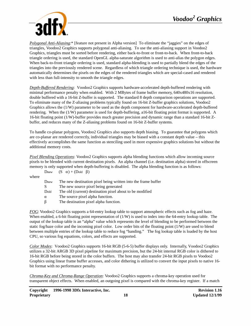
Polygonal Anti-Aliasing:* [feature not present in Alpha version] To eliminate the “jaggies” on the edges of triangles, Voodoo2 Graphics supports polygonal anti-aliasing. To use the anti-aliasing support in Voodoo2 Graphics, triangles must be sorted before rendering, either back-to-front or front-to-back. When front-to-back triangle ordering is used, the standard OpenGL alpha-saturate algorithm is used to anti-alias the polygon edges. When back-to-front triangle ordering is used, standard alpha-blending is used to partially blend the edges of the triangles into the previously rendered scene. Regardless of which triangle ordering technique is used, the hardware automatically determines the pixels on the edges of the rendered triangles which are special-cased and rendered with less than full-intensity to smooth the triangle edges. Depth-Buffered Rendering: Voodoo2 Graphics supports hardware-accelerated depth-buffered rendering with minimal performance penalty when enabled. With 2 MBytes of frame buffer memory, 640x480x16 resolution, double buffered with a 16-bit Z-buffer is supported. The standard 8 depth comparison operations are supported. To eliminate many of the Z-aliasing problems typically found on 16-bit Z-buffer graphics solutions, Voodoo2 Graphics allows the (1/W) parameter to be used as the depth component for hardware-accelerated depth-buffered rendering. When the (1/W) parameter is used for depth-buffering, a16-bit floating point format is supported. A 16-bit floating point (1/W)-buffer provides much greater precision and dynamic range than a standard 16-bit Z-buffer, and reduces many of the Z-aliasing problems found on 16-bit Z-buffer systems. To handle co-planar polygons, Voodoo2 Graphics also supports depth biasing. To guarantee that polygons which are co-planar are rendered correctly, individual triangles may be biased with a constant depth value – this effectively accomplishes the same function as stenciling used in more expensive graphics solutions but without the additional memory costs. Pixel Blending Operations: Voodoo2 Graphics supports alpha blending functions which allow incoming source pixels to be blended with current destination pixels. An alpha channel (i.e. destination alpha) stored in offscreen memory is only supported when depth-buffering is disabled. The alpha blending function is as follows:
Dnew ⇐ (S ⋅ α) + (Dold ⋅ β) where
Dnew The new destination pixel being written into the frame buffer S The new source pixel being generated Dold The old (current) destination pixel about to be modified α The source pixel alpha function. β The destination pixel alpha function.
FOG: Voodoo2 Graphics supports a 64-entry lookup table to support atmospheric effects such as fog and haze. When enabled, a 6-bit floating point representation of (1/W) is used to index into the 64-entry lookup table. The output of the lookup table is an “alpha” value which represents the level of blending to be performed between the static fog/haze color and the incoming pixel color. Low order bits of the floating point (1/W) are used to blend between multiple entries of the lookup table to reduce fog “banding.” The fog lookup table is loaded by the host CPU, so various fog equations, colors, and effects are supported. Color Modes: Voodoo2 Graphics supports 16-bit RGB (5-6-5) buffer displays only. Internally, Voodoo2 Graphics utilizes a 32-bit ARGB 3D pixel pipeline for maximum precision, but the 24-bit internal RGB color is dithered to 16-bit RGB before being stored in the color buffers. The host may also transfer 24-bit RGB pixels to Voodoo2 Graphics using linear frame buffer accesses, and color dithering is utilized to convert the input pixels to native 16-bit format with no performance penalty. Chroma-Key and Chroma-Range Operation: Voodoo2 Graphics supports a chroma-key operation used for transparent object effects. When enabled, an outgoing pixel is compared with the chroma-key register. If a match

Voodoo2 Graphics
Copyright 1996-1998 3Dfx Interactive, Inc. Revision 1.16 Proprietary 19 Updated 12/1/99
is detected, the outgoing pixel is invalidated in the pixel pipeline, and the frame buffer is not updated. In addition, a superset of chroma-keying, known as chroma-ranging, may be used. Instead of matching outgoing pixels against a single chroma-key color, chroma-ranging uses a range of colors for the comparison. If the outgoing pixel is within the range specified by the chroma-range registers and chroma-ranging is enabled, then the frame buffer is updated with the pixel. Color Dithering Operations: All operations internal to Voodoo2 Graphics operate in native 32-bit ARGB pixel mode. However, color dithering from the 24-bit RGB pixels to 16-bit RGB (5-6-5) pixels is provided on the back end of the pixel pipeline. Using the color dithering option, the host can pass 24-bit RGB pixels to Voodoo2 Graphics, which converts the incoming 24-bit RGB pixels to 16-bit RGB (5-6-5) pixels which are then stored in the 16-bit RGB buffer. The 16-bit color dithering allows for the generation of photorealistic images without the additional cost of a true color frame buffer storage area. 2D BitBLT Engine: Voodoo2 Graphics includes an optimized 2D BitBLT engine used for accelerating standard Windows GDI and DirectDraw primitives. Data can be transfered either from host-to-Screen or from Screen-to-Screen. Solid rectangular fills and copies are supported, in addition to color expansion of host-supplied text/glyph data. Chroma-ranging is supported for both source and destination pixels. All BitBLT operations may also optionally use the standard 16 Raster Operations (ROPs) to merge the source and destination pixels. In addition to the standard BiBLT 2D engine, Voodoo2 Graphics supports the color expansion capabilities of SGRAM* (SGRAM fill not implemented in Alpha version). When Voodoo2 Graphics is configured with SGRAMs, a special rectangle fill command is used to perform ultra-fast full-screen clears of the color and/or depth buffers. When utilizing the color expansion capabilities of SGRAM, Voodoo2 Graphics performs screen-clears at 16 pixels per clock, resulting in 1.2 GPixels/sec peak fill rate – this results in a full-screen clear time of either the color buffer or the depth buffer of approximately 260 usec at 640x480 resolution. Programmable Video Timing: Voodoo2 Graphics uses a programmable video timing controller which allows for very flexible video timing. Any monitor type may be used with Voodoo2 Graphics , with 76+ Hz vertical refresh rates supported at 800x600 resolution, and 100+ Hz vertical refresh rates supported at 640x480 resolution. Lower resolutions down to 320x200 are also supported. Video Output Gamma Correction: Voodoo2 Graphics uses a programmable color lookup table to allow for programmable gamma correction. The 16-bit dithered color data from the frame buffer is used an an index into the gamma-correction color table -- the 24-bit output of the gamma-correction color table is then fed to the monitor or Television. Direct Monitor and Television Output:* (not present in Alpha version and may be ommitted from spec) Voodoo2 Graphics includes an embedded RAMDAC and NTSC/PAL encoder to allow direct connection to a standard PC monitor or television. To eliminate the “flicker” typically associated with NTSC/PAL interlaced displays, Voodoo2 Graphics includes a programmable 3-tap vertical line filter for flicker reduction. While Voodoo2 Graphics can generate signals for direct connection to either a PC monitor or a television, the same DAC is used for both, so simultaneous PC-Monitor and Television output is not supported.

Voodoo2 Graphics
Copyright 1996-1998 3Dfx Interactive, Inc. Revision 1.16 Proprietary 20 Updated 12/1/99
4. Voodoo2 Graphics Address Space Voodoo2 Graphics requires 16 Mbytes of memory mapped address space. Voodoo2 Graphics does not utilize I/O mapped memory. The memory mapped address space is shown below:
Address Description 0x000000-0x3fffff Voodoo2 Graphics memory mapped register set (4 MBytes) 0x400000-0x7fffff Voodoo2 Graphics linear frame buffer access (4 MBytes) 0x800000-0xffffff Voodoo2 Graphics texture memory access (8 MBytes) The physical memory address for Voodoo2 Graphics accesses is calculated by adding the Voodoo2 Graphics address offset (0-16 MBytes) to the Voodoo2 Graphics base address register. The Voodoo2 Graphics base address register, memBaseAddr, is located in PCI configuration space. memBaseAddr is setup by the PCI System BIOS during system power-on initialization and should not be modified by software. See section 5 for more information on the memory mapped register set, section 6 for more information on the PCI configuration space, section 9 for more information on linear frame buffer access, and section 10 for more information on texture memory access.

Voodoo2 Graphics
Copyright 1996-1998 3Dfx Interactive, Inc. Revision 1.16 Proprietary 21 Updated 12/1/99
5. Memory Mapped Register Set A 4 Mbyte (22-bit) Voodoo2 Graphics memory mapped register address is divided into the following fields: Alternate
Register Mapping Byte Swizzle
Register Accesses
Wrap Chip Register Byte
1 bit (21) 1 bit (20) 6 bits (19:14) 4 bits (13:10) 8 bits (9:2) 2 bits (1:0) The Alternate Register Mapping bit (bit 21) of the memory mapped register address is used to select the alternate register mapping (see below). When fbiInit3(0)=1 and bit 21 of the memory mapped register address is set, the alternate register mapping is used. The Byte Swizzle Register Accesses bit (bit 20) of the memory mapped register address is used to byte-swizzle the PCI data for both register reads and register writes. When fbiInit0(3)=1 and bit 20 of the memory mapped register address is set, then byte 3 of the PCI data is swapped with byte 0, and byte 2 of the PCI data is swapped with byte 1. This byte-swizzling capability is used to support big-endian host CPUs. The wrap field aliases multiple 14-bit register maps. The wrap field is useful for processors such as the Digital’s Alpha or Intel’s Pentium Pro which contain large write-buffers which collapse multiple writes to the same address into a single write (an undesirable effect when programming Voodoo2 Graphics). By writing to different wraps, software can guarantee that writes are not collapsed in the write buffer. Note that Voodoo2 Graphics functionality is identical regardless of which wrap is accessed. The chip field selects one or more of the Voodoo2 Graphics chips (Chuck and/or Bruce) to be accessed. Each bit in the chip field selects one chip for writing, with Chuck controlled by the lsb of the chip field, and Bruce#2 controlled by the msb of the chip field. Note the chip field value of 0x0 selects all chips. The following table shows the chip field mappings: Chip Field Voodoo2 Graphics Chip
Accessed 0000 Chuck + all Bruce chips 0001 Chuck 0010 Bruce #0 0011 Chuck + Bruce #0 0100 Bruce #1 0101 Chuck + Bruce #1 0110 Bruce #0 + Bruce #1 0111 Chuck + Bruce #0 + Bruce #1 1000 Bruce #2 1001 Chuck + Bruce #2 1010 Bruce #0 + Bruce #2 1011 Chuck + Bruce #0 + Bruce #2 1100 Bruce #1 + Bruce #2 1101 Chuck + Bruce #1 + Bruce #2 1110 Bruce #0 + Bruce #1 + Bruce #2 1111 Chuck + all Bruce chips Note that Bruce #0 is always connected to Chuck in the system level diagrams of section 3, and Bruce #1 is attached to Bruce #0, etc. By utilizing the different chip fields, software can precisely control the data presented to

Voodoo2 Graphics
Copyright 1996-1998 3Dfx Interactive, Inc. Revision 1.16 Proprietary 22 Updated 12/1/99
individual chips which compose the Voodoo2 Graphics graphics subsystem. Note that for reads, the chip field is ignored, and read data is always read from Chuck. The register field selects the register to be accessed from the table below. All accesses to the memory mapped registers must be 32-bit accesses. No byte (8-bit) or halfword/short (16-bit) accesses are allowed to the memory mapped registers, so the byte (2-bit) field of all memory mapped register accesses must be 0x0. As a result, to modify individual bits of a 32-bit register, the entire 32-bit word must be written with valid bits in all positions. The table below shows the Voodoo2 Graphics register set. The register set shown below is the address map when the triangle registers are not remapped (fbiInit3(0)=0 or bit 21 of the memory mapped register address is 0). The chip column illustrates which registers are stored in which chips. For the registers which are stored in Bruce, the % symbol specifies that the register is unconditionally written to Bruce regardless of the chip address. Similarly, the * symbol specifies that the register is only written to a given Bruce if specified in the chip address. The R/W column illustrates the read/write status of individual registers. Reading from a register which is “write only” returns undefined data. Also, reading from a register that is Bruce specific returns undefined data.. Reads from all other memory mapped registers only contain valid data in the bits stored by the registers, and undefined/reserved bits in a given register must be masked by software. The pipelined column indicates whether the graphics processor must wait for the current command to finish before loading a particular register from the FIFO. A “no” in the pipelined column means the graphics processor flushes the data pipeline before loading the register -- this results in a small performance degradation when compared to those registers which do not need synchronization. The FIFO column indicates whether a write to a particular register is pushed onto the PCI bus FIFO. Care must be taken when writing to those registers not pushed into the FIFO in order to prevent race conditions between FIFOed and non-FIFOed registers. Also note that reads are not pushed into the PCI bus FIFO, and reading FIFOed registers returns the current value of the register, irrespective of pending writes to the register present in the FIFO.
Register Name Address Bits Chip R/W
Pipe-lined?
/FIFO?
Description
status 0x000(0) 31:0 Chuck R Yes / n/a Voodoo2 Graphics Status intrCtrl 0x004(4) 31:0 Chuck R/W Yes / No Interrupt Status and Control vertexAx 0x008(8) 15:0 Chuck+Bruce% W Yes / Yes Vertex A x-coordinate location (12.4 format) vertexAy 0x00c(12) 15:0 Chuck+Bruce% W Yes / Yes Vertex A y-coordinate location (12.4 format) vertexBx 0x010(16) 15:0 Chuck+Bruce% W Yes / Yes Vertex B x-coordinate location (12.4 format) vertexBy 0x014(20) 15:0 Chuck+Bruce% W Yes / Yes Vertex B y-coordinate location (12.4 format) vertexCx 0x018(24) 15:0 Chuck+Bruce% W Yes / Yes Vertex C x-coordinate location (12.4 format) vertexCy 0x01c(28) 15:0 Chuck+Bruce% W Yes / Yes Vertex C y-coordinate location (12.4 format) startR 0x020(32) 23:0 Chuck W Yes / Yes Starting Red parameter (12.12 format) startG 0x024(36) 23:0 Chuck W Yes / Yes Starting Green parameter (12.12 format) startB 0x028(40) 23:0 Chuck W Yes / Yes Starting Blue parameter (12.12 format) startZ 0x02c(44) 31:0 Chuck W Yes / Yes Starting Z parameter (20.12 format) startA 0x030(48) 23:0 Chuck W Yes / Yes Starting Alpha parameter (12.12 format) startS 0x034(52) 31:0 Bruce* W Yes / Yes Starting S/W parameter (14.18 format) startT 0x038(56) 31:0 Bruce* W Yes / Yes Starting T/W parameter (14.18 format) startW 0x03c(60) 31:0 Chuck+Bruce* W Yes / Yes Starting 1/W parameter (2.30 format) dRdX 0x040(64) 23:0 Chuck W Yes / Yes Change in Red with respect to X (12.12 format) dGdX 0x044(68) 23:0 Chuck W Yes / Yes Change in Green with respect to X (12.12 format) dBdX 0x048(72) 23:0 Chuck W Yes / Yes Change in Blue with respect to X (12.12 format) dZdX 0x04c(76) 31:0 Chuck W Yes / Yes Change in Z with respect to X (20.12 format) dAdX 0x050(80) 23:0 Chuck W Yes / Yes Change in Alpha with respect to X (12.12 format)

Voodoo2 Graphics
Copyright 1996-1998 3Dfx Interactive, Inc. Revision 1.16 Proprietary 23 Updated 12/1/99
dSdX 0x054(84) 31:0 Bruce* W Yes / Yes Change in S/W with respect to X (14.18 format) dTdX 0x058(88) 31:0 Bruce* W Yes / Yes Change in T/W with respect to X (14.18 format) dWdX 0x05c(92) 31:0 Chuck+Bruce* W Yes / Yes Change in 1/W with respect to X (2.30 format) dRdY 0x060(96) 23:0 Chuck W Yes / Yes Change in Red with respect to Y (12.12 format) dGdY 0x064(100) 23:0 Chuck W Yes / Yes Change in Green with respect to Y (12.12 format) dBdY 0x068(104) 23:0 Chuck W Yes / Yes Change in Blue with respect to Y (12.12 format) dZdY 0x06c(108) 31:0 Chuck W Yes / Yes Change in Z with respect to Y (20.12 format) dAdY 0x070(112) 23:0 Chuck W Yes / Yes Change in Alpha with respect to Y (12.12 format) dSdY 0x074(116) 31:0 Bruce* W Yes / Yes Change in S/W with respect to Y (14.18 format) dTdY 0x078(120) 31:0 Bruce* W Yes / Yes Change in T/W with respect to Y (14.18 format) dWdY 0x07c(124) 31:0 Chuck+Bruce* W Yes / Yes Change in 1/W with respect to Y (2.30 format) triangleCMD 0x080(128) 31 Chuck+Bruce% W Yes / Yes Execute TRIANGLE command (floating point) reserved 0x084(132) n/a n/a W n/a fvertexAx 0x088(136) 31:0 Chuck+Bruce% W Yes / Yes Vertex A x-coordinate location (floating point) fvertexAy 0x08c(140) 31:0 Chuck+Bruce% W Yes / Yes Vertex A y-coordinate location (floating point) fvertexBx 0x090(144) 31:0 Chuck+Bruce% W Yes / Yes Vertex B x-coordinate location (floating point) fvertexBy 0x094(148) 31:0 Chuck+Bruce% W Yes / Yes Vertex B y-coordinate location (floating point) fvertexCx 0x098(152) 31:0 Chuck+Bruce% W Yes / Yes Vertex C x-coordinate location (floating point) fvertexCy 0x09c(156) 31:0 Chuck+Bruce% W Yes / Yes Vertex C y-coordinate location (floating point) fstartR 0x0a0(160) 31:0 Chuck W Yes / Yes Starting Red parameter (floating point) fstartG 0x0a4(164) 31:0 Chuck W Yes / Yes Starting Green parameter (floating point) fstartB 0x0a8(168) 31:0 Chuck W Yes / Yes Starting Blue parameter (floating point) fstartZ 0x0ac(172) 31:0 Chuck W Yes / Yes Starting Z parameter (floating point) fstartA 0x0b0(176) 31:0 Chuck W Yes / Yes Starting Alpha parameter (floating point) fstartS 0x0b4(180) 31:0 Bruce* W Yes / Yes Starting S/W parameter (floating point) fstartT 0x0b8(184) 31:0 Bruce* W Yes / Yes Starting T/W parameter (floating point) fstartW 0x0bc(188) 31:0 Chuck+Bruce* W Yes / Yes Starting 1/W parameter (floating point) fdRdX 0x0c0(192) 31:0 Chuck W Yes / Yes Change in Red with respect to X (floating point) fdGdX 0x0c4(196) 31:0 Chuck W Yes / Yes Change in Green with respect to X (floating
point) fdBdX 0x0c8(200) 31:0 Chuck W Yes / Yes Change in Blue with respect to X (floating point) fdZdX 0x0cc(204) 31:0 Chuck W Yes / Yes Change in Z with respect to X (floating point) fdAdX 0x0d0(208) 31:0 Chuck W Yes / Yes Change in Alpha with respect to X (floating point) fdSdX 0x0d4(212) 31:0 Bruce* W Yes / Yes Change in S/W with respect to X (floating point) fdTdX 0x0d8(216) 31:0 Bruce* W Yes / Yes Change in T/W with respect to X (floating point) fdWdX 0x0dc(220) 31:0 Chuck+Bruce* W Yes / Yes Change in 1/W with respect to X (floating point) fdRdY 0x0e0(224) 31:0 Chuck W Yes / Yes Change in Red with respect to Y (floating point) fdGdY 0x0e4(228) 31:0 Chuck W Yes / Yes Change in Green with respect to Y (floating
point) fdBdY 0x0e8(232) 31:0 Chuck W Yes / Yes Change in Blue with respect to Y (floating point) fdZdY 0x0ec(236) 31:0 Chuck W Yes / Yes Change in Z with respect to Y (floating point) fdAdY 0x0f0(240) 31:0 Chuck W Yes / Yes Change in Alpha with respect to Y (floating point) fdSdY 0x0f4(244) 31:0 Bruce* W Yes / Yes Change in S/W with respect to Y (floating point) fdTdY 0x0f8(248) 31:0 Bruce* W Yes / Yes Change in T/W with respect to Y (floating point) fdWdY 0x0fc(252) 31:0 Chuck+Bruce* W Yes / Yes Change in 1/W with respect to Y (floating point) ftriangleCMD 0x100(256) 31 Chuck+Bruce% W Yes / Yes Execute TRIANGLE command (floating point)

Voodoo2 Graphics
Copyright 1996-1998 3Dfx Interactive, Inc. Revision 1.16 Proprietary 24 Updated 12/1/99
fbzColorPath 0x104(260) 29:0 Chuck+Bruce% R/W Yes / Yes Chuck Color Path Control fogMode 0x108(264) 7:0 Chuck R/W Yes / Yes Fog Mode Control alphaMode 0x10c(268) 31:0 Chuck R/W Yes / Yes Alpha Mode Control fbzMode 0x110(272) 21:0 Chuck R/W No / Yes RGB Buffer and Depth-Buffer Control lfbMode 0x114(276) 16:0 Chuck R/W No / Yes Linear Frame Buffer Mode Control clipLeftRight 0x118(280) 31:0 Chuck R/W No / Yes Left and Right of Clipping Register clipLowYHighY 0x11c(284) 31:0 Chuck R/W No / Yes Top and Bottom of Clipping Register nopCMD 0x120(288) 1:0 Chuck+Bruce% W No / Yes Execute NOP command fastfillCMD 0x124(292) n/a Chuck W No / Yes Execute FASTFILL command swapbufferCMD 0x128(296) 9:0 Chuck W No / Yes Execute SWAPBUFFER command fogColor 0x12c(300) 23:0 Chuck W No / Yes Fog Color Value zaColor 0x130(304) 31:0 Chuck W No / Yes Constant Alpha/Depth Value chromaKey 0x134(308) 23:0 Chuck+Bruce* W No / Yes Chroma Key Compare Value chromaRange 0x138(312) 27:0 Chuck+Bruce* W No / Yes Chroma Range Compare Values,modes,enable userIntrCMD 0x13c(316) 9:0 Chuck W No / Yes Execute USERINTERRUPT command stipple 0x140(320) 31:0 Chuck R/W No / Yes Rendering Stipple Value color0 0x144(324) 31:0 Chuck R/W No / Yes Constant Color #0 color1 0x148(328) 31:0 Chuck R/W No / Yes Constant Color #1 fbiPixelsIn 0x14c(332) 23:0 Chuck R n/a Pixel Counter (Number pixels processed) fbiChromaFail 0x150(336) 23:0 Chuck R n/a Pixel Counter (Number pixels failed Chroma test) fbiZfuncFail 0x154(340) 23:0 Chuck R n/a Pixel Counter (Number pixels failed Z test) fbiAfuncFail 0x158(344) 23:0 Chuck R n/a Pixel Counter (Number pixels failed Alpha test) fbiPixelsOut 0x15c(348) 23:0 Chuck R n/a Pixel Counter (Number pixels drawn) fogTable 0x160(352)
to 0x1dc(476)
31:0 Chuck W No / Yes Fog Table
cmdFifoBaseAddr 0x1e0(480) 25:0 Chuck R/W (n/a) / No CMDFIFO base address and size cmdFifoBump 0x1e4(484) 15:0 Chuck R/W (n/a) / No CMDFIFO bump depth cmdFifoRdPtr 0x1e8(488) 31:0 Chuck R/W (n/a) / No CMDFIFO current read pointer cmdFifoAMin 0x1ec(492) 31:0 Chuck R/W (n/a) / No CMDFIFO current minimum address cmdFifoAMax 0x1f0(496) 31:0 Chuck R/W (n/a) / No CMDFIFO current maximum address cmdFifoDepth 0x1f4(500) 15:0 Chuck R/W (n/a) / No CMDFIFO current depth cmdFifoHoles 0x1f8(504) 15:0 Chuck R/W (n/a) / No CMDFIFO number of holes reserved 0x1fc(508) n/a n/a n/a n/a fbiInit4 0x200(512) 12:0 Chuck R/W (n/a) / No Chuck Hardware Initialization (register 4) vRetrace 0x204(516) 12:0 Chuck R (n/a) / No Vertical Retrace Counter backPorch 0x208(520) 24:0 Chuck R/W (n/a) / No Video Backporch Timing Generator videoDimensions 0x20c(524) 26:0 Chuck R/W (n/a) / No Video Screen Dimensions fbiInit0 0x210(528) 31:0 Chuck R/W (n/a) / No Chuck Hardware Initialization (register 0) fbiInit1 0x214(532) 31:0 Chuck R/W (n/a) / No Chuck Hardware Initialization (register 1) fbiInit2 0x218(536) 31:0 Chuck R/W (n/a) / No Chuck Hardware Initialization (register 2) fbiInit3 0x21c(540) 31:0 Chuck R/W (n/a) / No Chuck Hardware Initialization (register 3) hSync 0x220(544) 26:0 Chuck W (n/a) / No Horizontal Sync Timing Generator vSync 0x224(548) 28:0 Chuck W (n/a) / No Vertical Sync Timing Generator clutData 0x228(552) 29:0 Chuck W No / Yes Video Color Lookup Table Initialization dacData 0x22c(556) 13:0 Chuck W (n/a) / No External DAC Initialization

Voodoo2 Graphics
Copyright 1996-1998 3Dfx Interactive, Inc. Revision 1.16 Proprietary 25 Updated 12/1/99
maxRgbDelta 0x230(560) 23:0 Chuck W (n/a) / No Max. RGB difference for Video Filtering hBorder 0x234(564) 24:0 Chuck W (n/a) / No Horizontal Border Color Control vBorder 0x238(568) 24:0 Chuck W (n/a) / No Vertical Border Color Control borderColor 0x23c(572) 23:0 Chuck W (n/a) / No Video Border Color hvRetrace 0x240(576) 26:0 Chuck R (n/a) / No Horizontal and Vertical Retrace Counters
(synced) fbiInit5 0x244(580) 31:0 Chuck R/W (n/a) / No Chuck Hardware Initialization (register 5) fbiInit6 0x248(584) 31:0 Chuck R/W (n/a) / No Chuck Hardware Initialization (register 6) fbiInit7 0x24c(588) 31:0 Chuck R/W (n/a) / No Chuck Hardware Initialization (register 7) reserved 0x250(592) n/a n/a n/a n/a reserved 0x254(596) n/a n/a n/a n/a fbiSwapHistory 0x258(600) 31:0 Chuck R n/a Swap History Register fbiTrianglesOut 0x25c(604) 23:0 Chuck R n/a Triangle Counter (Number triangles drawn) sSetupMode 0x260(608) 19:0 Chuck W Yes / Yes Triangle setup mode sVx 0x264(612) 31:0 Chuck+Bruce* W Yes / Yes Triangle setup X sVy 0x268(616) 31:0 Chuck+Bruce* W Yes / Yes Triangle setup Y sARGB 0x26c(620) 31:0 Chuck+Bruce* W Yes / Yes Triangle setup Alpha, Red, Green, Blue sRed 0x270(624) 31:0 Chuck W Yes / Yes Triangle setup Red value sGreen 0x274(628) 31:0 Chuck W Yes / Yes Triangle setup Green value sBlue 0x278(632) 31:0 Chuck W Yes / Yes Triangle setup Blue value sAlpha 0x27c(636) 31:0 Chuck W Yes / Yes Triangle setup Alpha value sVz 0x280(640) 31:0 Chuck W Yes / Yes Triangle setup Z sWb 0x284(644) 31:0 Chuck+Bruce* W Yes / Yes Triangle setup Global W sWtmu0 0x288(648) 31:0 Bruce* W Yes / Yes Triangle setup Tmu0 & Tmu1 W sS/W0 0x28c(652) 31:0 Bruce* W Yes / Yes Triangle setup Tmu0 & Tmu1 S/W sT/W0 0x290(656) 31:0 Bruce* W Yes / Yes Triangle setup Tmu0 & Tmu1 T/W sWtmu1 0x294(660) 31:0 Bruce-1 W Yes / Yes Triangle setup Tmu1 only W sS/Wtmu1 0x298(664) 31:0 Bruce-1 W Yes / Yes Triangle setup Tmu1 only S/W sT/Wtmu1 0x29c(668) 31:0 Bruce-1 W Yes / Yes Triangle setup Tmu1 only T/W sDrawTriCMD 0x2a0(672) 31:0 Chuck+Bruce* W Yes / Yes Triangle setup (Draw) sBeginTriCMD 0x2a4(676) 31:0 Chuck W Yes / Yes Triangle setup Start New triangle reserved 0x2a8(680) n/a n/a n/a n/a reserved 0x2ac(684) n/a n/a n/a n/a reserved 0x2b0(688) n/a n/a n/a n/a reserved 0x2b4(692) n/a n/a n/a n/a reserved 0x2b8(696) n/a n/a n/a n/a reserved 0x2bc(700) n/a n/a n/a n/a bltSrcBaseAddr 0x2c0(704) 21:0 Chuck R/W Yes / Yes BitBLT Source base address bltDstBaseAddr 0x2c4(708) 21:0 Chuck R/W Yes / Yes BitBLT Destination base address bltXYStrides 0x2c8(712) 27:0 Chuck R/W Yes / Yes BitBLT Source and Destination strides bltSrcChromaRange 0x2cc(716) 31:0 Chuck R/W Yes / Yes BiBLT Source Chroma key range bltDstChromaRange 0x2d0(720) 31:0 Chuck R/W Yes / Yes BitBLT Destination Chroma key range bltClipX 0x2d4(724) 27:0 Chuck R/W Yes / Yes BitBLT Min/Max X clip values bltClipY 0x2d8(728) 27:0 Chuck R/W Yes / Yes BitBLT Min/Max Y clip values reserved 0x2dc(732) bltSrcXY 0x2e0(736) 26:0 Chuck R/W Yes / Yes BitBLT Source starting XY coordinates
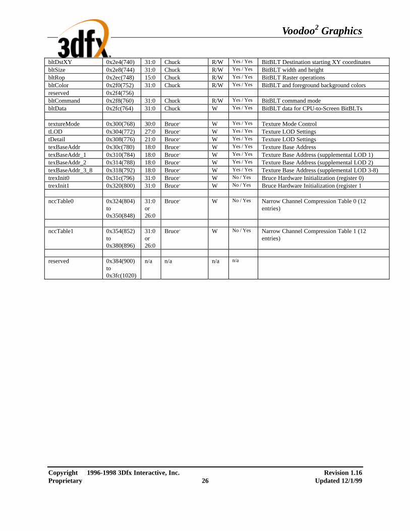
Voodoo2 Graphics
Copyright 1996-1998 3Dfx Interactive, Inc. Revision 1.16 Proprietary 26 Updated 12/1/99
bltDstXY 0x2e4(740) 31:0 Chuck R/W Yes / Yes BitBLT Destination starting XY coordinates bltSize 0x2e8(744) 31:0 Chuck R/W Yes / Yes BitBLT width and height bltRop 0x2ec(748) 15:0 Chuck R/W Yes / Yes BitBLT Raster operations bltColor 0x2f0(752) 31:0 Chuck R/W Yes / Yes BitBLT and foreground background colors reserved 0x2f4(756) bltCommand 0x2f8(760) 31:0 Chuck R/W Yes / Yes BitBLT command mode bltData 0x2fc(764) 31:0 Chuck W Yes / Yes BitBLT data for CPU-to-Screen BitBLTs textureMode 0x300(768) 30:0 Bruce* W Yes / Yes Texture Mode Control tLOD 0x304(772) 27:0 Bruce* W Yes / Yes Texture LOD Settings tDetail 0x308(776) 21:0 Bruce* W Yes / Yes Texture LOD Settings texBaseAddr 0x30c(780) 18:0 Bruce* W Yes / Yes Texture Base Address texBaseAddr_1 0x310(784) 18:0 Bruce* W Yes / Yes Texture Base Address (supplemental LOD 1) texBaseAddr_2 0x314(788) 18:0 Bruce* W Yes / Yes Texture Base Address (supplemental LOD 2) texBaseAddr_3_8 0x318(792) 18:0 Bruce* W Yes / Yes Texture Base Address (supplemental LOD 3-8) trexInit0 0x31c(796) 31:0 Bruce* W No / Yes Bruce Hardware Initialization (register 0) trexInit1 0x320(800) 31:0 Bruce* W No / Yes Bruce Hardware Initialization (register 1 nccTable0 0x324(804)
to 0x350(848)
31:0 or 26:0
Bruce* W No / Yes Narrow Channel Compression Table 0 (12 entries)
nccTable1 0x354(852)
to 0x380(896)
31:0 or 26:0
Bruce* W No / Yes Narrow Channel Compression Table 1 (12 entries)
reserved 0x384(900)
to 0x3fc(1020)
n/a n/a n/a n/a

Voodoo2 Graphics
Copyright 1996-1998 3Dfx Interactive, Inc. Revision 1.16 Proprietary 27 Updated 12/1/99
When fbiinit3(0)=1, the triangle parameter registers can be aliased to a different address mapping to improve PCI bus throughput. When fbiinit3(0)=1 and the upper bit of the wrap field in the pci address is 0x1 (pci_ad[21]=1), the following table shows the addresses for the triangle parameter registers. Note that enabling triangle parameter remapping (fbiinit3(0)=1) has no affect any registers not specified in the table below. Register Name Address Bits Chip R/W Pipe-
lined? /FIFO?
Description
status 0x000(0) 31:0 Chuck R/W Yes / Yes
Voodoo2 Graphics Status
reserved 0x004(4) n/a n/a n/a n/a vertexAx 0x008(8) 15:0 Chuck+Bruce% W Yes /
Yes Vertex A x-coordinate location (12.4 format)
vertexAy 0x00c(12) 15:0 Chuck+Bruce% W Yes / Yes
Vertex A y-coordinate location (12.4 format)
vertexBx 0x010(16) 15:0 Chuck+Bruce% W Yes / Yes
Vertex B x-coordinate location (12.4 format)
vertexBy 0x014(20) 15:0 Chuck+Bruce% W Yes / Yes
Vertex B y-coordinate location (12.4 format)
vertexCx 0x018(24) 15:0 Chuck+Bruce% W Yes / Yes
Vertex C x-coordinate location (12.4 format)
vertexCy 0x01c(28) 15:0 Chuck+Bruce% W Yes / Yes
Vertex C y-coordinate location (12.4 format)
startR 0x020(32) 23:0 Chuck W Yes /
Yes Starting Red parameter (12.12 format)
dRdX 0x024(36) 23:0 Chuck W Yes / Yes
Change in Red with respect to X (12.12 format)
dRdY 0x028(40) 23:0 Chuck W Yes / Yes
Change in Red with respect to Y (12.12 format)
startG 0x02c(44) 23:0 Chuck W Yes / Yes
Starting Green parameter (12.12 format)
dGdX 0x030(48) 23:0 Chuck W Yes / Yes
Change in Green with respect to X (12.12 format)
dGdY 0x034(52) 23:0 Chuck W Yes / Yes
Change in Green with respect to Y (12.12 format)
startB 0x038(56) 23:0 Chuck W Yes / Yes
Starting Blue parameter (12.12 format)
dBdX 0x03c(60) 23:0 Chuck W Yes / Yes
Change in Blue with respect to X (12.12 format)
dBdY 0x040(64) 23:0 Chuck W Yes /
Yes Change in Blue with respect to Y (12.12 format)
startZ 0x044(68) 31:0 Chuck W Yes / Yes
Starting Z parameter (20.12 format)
dZdX 0x048(72) 31:0 Chuck W Yes / Yes
Change in Z with respect to X (20.12 format)
dZdY 0x04c(76) 31:0 Chuck W Yes / Yes
Change in Z with respect to Y (12.12 format)
startA 0x050(80) 23:0 Chuck W Yes / Yes
Starting Alpha parameter (12.12 format)
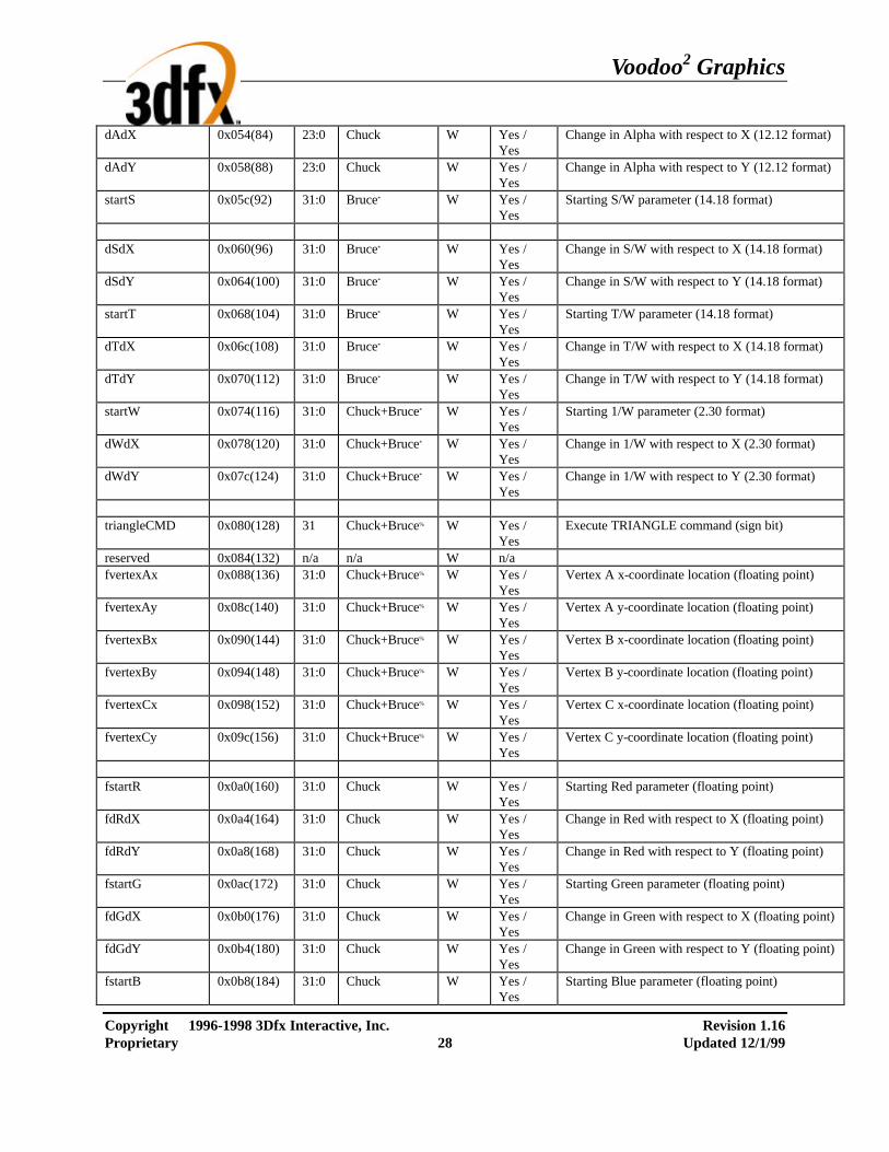
Voodoo2 Graphics
Copyright 1996-1998 3Dfx Interactive, Inc. Revision 1.16 Proprietary 28 Updated 12/1/99
dAdX 0x054(84) 23:0 Chuck W Yes / Yes
Change in Alpha with respect to X (12.12 format)
dAdY 0x058(88) 23:0 Chuck W Yes / Yes
Change in Alpha with respect to Y (12.12 format)
startS 0x05c(92) 31:0 Bruce* W Yes / Yes
Starting S/W parameter (14.18 format)
dSdX 0x060(96) 31:0 Bruce* W Yes /
Yes Change in S/W with respect to X (14.18 format)
dSdY 0x064(100) 31:0 Bruce* W Yes / Yes
Change in S/W with respect to Y (14.18 format)
startT 0x068(104) 31:0 Bruce* W Yes / Yes
Starting T/W parameter (14.18 format)
dTdX 0x06c(108) 31:0 Bruce* W Yes / Yes
Change in T/W with respect to X (14.18 format)
dTdY 0x070(112) 31:0 Bruce* W Yes / Yes
Change in T/W with respect to Y (14.18 format)
startW 0x074(116) 31:0 Chuck+Bruce* W Yes / Yes
Starting 1/W parameter (2.30 format)
dWdX 0x078(120) 31:0 Chuck+Bruce* W Yes / Yes
Change in 1/W with respect to X (2.30 format)
dWdY 0x07c(124) 31:0 Chuck+Bruce* W Yes / Yes
Change in 1/W with respect to Y (2.30 format)
triangleCMD 0x080(128) 31 Chuck+Bruce% W Yes /
Yes Execute TRIANGLE command (sign bit)
reserved 0x084(132) n/a n/a W n/a fvertexAx 0x088(136) 31:0 Chuck+Bruce% W Yes /
Yes Vertex A x-coordinate location (floating point)
fvertexAy 0x08c(140) 31:0 Chuck+Bruce% W Yes / Yes
Vertex A y-coordinate location (floating point)
fvertexBx 0x090(144) 31:0 Chuck+Bruce% W Yes / Yes
Vertex B x-coordinate location (floating point)
fvertexBy 0x094(148) 31:0 Chuck+Bruce% W Yes / Yes
Vertex B y-coordinate location (floating point)
fvertexCx 0x098(152) 31:0 Chuck+Bruce% W Yes / Yes
Vertex C x-coordinate location (floating point)
fvertexCy 0x09c(156) 31:0 Chuck+Bruce% W Yes / Yes
Vertex C y-coordinate location (floating point)
fstartR 0x0a0(160) 31:0 Chuck W Yes /
Yes Starting Red parameter (floating point)
fdRdX 0x0a4(164) 31:0 Chuck W Yes / Yes
Change in Red with respect to X (floating point)
fdRdY 0x0a8(168) 31:0 Chuck W Yes / Yes
Change in Red with respect to Y (floating point)
fstartG 0x0ac(172) 31:0 Chuck W Yes / Yes
Starting Green parameter (floating point)
fdGdX 0x0b0(176) 31:0 Chuck W Yes / Yes
Change in Green with respect to X (floating point)
fdGdY 0x0b4(180) 31:0 Chuck W Yes / Yes
Change in Green with respect to Y (floating point)
fstartB 0x0b8(184) 31:0 Chuck W Yes / Yes
Starting Blue parameter (floating point)

Voodoo2 Graphics
Copyright 1996-1998 3Dfx Interactive, Inc. Revision 1.16 Proprietary 29 Updated 12/1/99
fdBdX 0x0bc(188) 31:0 Chuck W Yes / Yes
Change in Blue with respect to X (floating point)
fdBdY 0x0c0(192) 31:0 Chuck W Yes /
Yes Change in Blue with respect to Y (floating point)
fstartZ 0x0c4(196) 31:0 Chuck W Yes / Yes
Starting Z parameter (floating point)
fdZdX 0x0c8(200) 31:0 Chuck W Yes / Yes
Change in Z with respect to X (floating point)
fdZdY 0x0cc(204) 31:0 Chuck W Yes / Yes
Change in Z with respect to Y (floating point)
fstartA 0x0d0(208) 31:0 Chuck W Yes / Yes
Starting Alpha parameter (floating point)
fdAdX 0x0d4(212) 31:0 Chuck W Yes / Yes
Change in Alpha with respect to X (floating point)
fdAdY 0x0d8(216) 31:0 Chuck W Yes / Yes
Change in Alpha with respect to Y (floating point)
fstartS 0x0dc(220) 31:0 Bruce* W Yes / Yes
Starting S/W parameter (floating point)
fdSdX 0x0e0(224) 31:0 Bruce* W Yes /
Yes Change in S/W with respect to X (floating point)
fdSdY 0x0e4(228) 31:0 Bruce* W Yes / Yes
Change in S/W with respect to Y (floating point)
fstartT 0x0e8(232) 31:0 Bruce* W Yes / Yes
Starting T/W parameter (floating point)
fdTdX 0x0ec(236) 31:0 Bruce* W Yes / Yes
Change in T/W with respect to X (floating point)
fdTdY 0x0f0(240) 31:0 Bruce* W Yes / Yes
Change in T/W with respect to Y (floating point)
fstartW 0x0f4(244) 31:0 Chuck+Bruce* W Yes / Yes
Starting 1/W parameter (floating point)
fdWdX 0x0f8(248) 31:0 Chuck+Bruce* W Yes / Yes
Change in 1/W with respect to X (floating point)
fdWdY 0x0fc(252) 31:0 Chuck+Bruce* W Yes / Yes
Change in 1/W with respect to Y (floating point)
ftriangleCMD 0x100(256) 31 Chuck+Bruce% W Yes /
Yes Execute TRIANGLE command (floating point)
5.1 status Register The status register provides a way for the CPU to interrogate the graphics processor about its current state and FIFO availability. The status register is read only and writing to status has no effect. Bit Description 5:0 PCI FIFO freespace (0x3f=FIFO empty). Default is 0x3f. 6 Vertical retrace (0=Vertical retrace active, 1=Vertical retrace inactive). Default is 1. 7 Chuck graphics engine busy (0=engine idle, 1=engine busy). Default is 0. 8 Bruce busy (0=engine idle, 1=engine busy). Default is 0. 9 Voodoo2 Graphics busy (0=idle, 1=busy). Default is 0. 11:10 Displayed buffer (0=buffer 0, 1=buffer 1, 2=auxiliary buffer, 3=reserved). Default is 0. 27:12 Memory FIFO freespace (0xffff=FIFO empty). Default is 0xffff.

Voodoo2 Graphics
Copyright 1996-1998 3Dfx Interactive, Inc. Revision 1.16 Proprietary 30 Updated 12/1/99
30:28 Swap Buffers Pending. Default is 0x0. 31 reserved Bits(5:0) show the number of entries available in the internal host FIFO. The internal host FIFO is 64 entries deep. The FIFO is empty when bits(5:0)=0x3f. Bit(6) is the state of the monitor vertical retrace signal, and is used to determine when the monitor is being refreshed. Bit(7) of status is used to determine if the graphics engine of Chuck is active. Note that bit(7) only determines if the graphics engine of Chuck is busy -- it does not include information as to the status of the internal PCI FIFOs. Bit(8) of status is used to determine if Bruce is busy. Note that bit(8) of status is set if any unit in Bruce is not idle -- this includes the graphics engine and all internal Bruce FIFOs. Bit(9) of status determines if all units in the Voodoo2 Graphics system (including graphics engines, FIFOs, etc.) are idle. Bit(9) is set when any internal unit in Voodoo2 Graphics is active (e.g. graphics is being rendered or any FIFO is not empty). Bits(11:10) show which RGB buffer is used for monitor refresh. Voodoo2 Graphics uses the values of bits(11:10) to determine the source of the RGB data that is sent to the monitor. When the Memory FIFO is enabled, bits(27:12) show the number of entries available in the Memory FIFO. Depending upon the amount of frame buffer memory available, a maximum of 65,536 entries may be stored in the Memory FIFO. The Memory FIFO is empty when bits(27:12)=0xffff. Bits (30:28) of status track the number of outstanding SWAPBUFFER commands. When a SWAPBUFFER command is received from the host cpu, bits (30:28) are incremented -- when a SWAPBUFFER command completes, bits (30:28) are decremented.
5.2 intrCtrl Register The intrCtrl register controls the interrupt capabilities of Voodoo2 Graphics. Bits 1:0 enable video horizontal sync signal generation of interrupts. Generated horizontal sync interrupts are detected by the CPU by reading bits 7:6 of intrCtrl. Bits 3:2 enable video vertical sync signal generation of interrupts. Generated vertical sync interrupts are detected by the CPU by reading bits 9:8 of intrCtrl. Bit 4 of intrCtrl enables generation of interrupts when the frontend PCI FIFO is full. Generated PCI FIFO Full interrupts are detected by the CPU by reading bit 10 of intrCtrl. PCI FIFO full interrupts are genered when intrCtrl bit 4 is set and the number of free entries in the frontend PCI FIFO drops below the value specified in fbiInit0 bits(10:6). Bit 5 of intrCtrl enables the user interrupt command USERINTERRUPT generation of interrupts. Generated user interrupts are detected by the CPU by reading bit 11 of intrCtrl. The tag associated with a generated user interrupt is stored in bits 19:12 of intrCtrl. Generated interrupts are cleared by writing a 0 to the bit signaling a particular interrupt was generated and writing a 1 to interCtrl bit(31). For example, a PCI FIFO full generated interrupt is cleared by writing a 0 to bit 10 of intrCtrl, and a generated user interrupt is cleared by writing a 0 to bit 11 of intrCtrl. For both cases, bit 31 of intrCtrl must be written with the value 1 to clear the external PCI interrupt. Care must be taken when clearing interrupts not to accidentally overwrite the interrupt mask bits (bits 5:0) of intrCtrl) which enable generation of particular interrupts. Note that writes to the intrCtrl register are not pushed on the PCI frontend FIFO, so writes to intrCtrl are processed immediately. Since intrCtrl is not FIFO’ed, writes to intrCtrl may be processed out-of-order with respect to other queued writes in the PCI and memory-backed FIFOs. Also note that PCI configuration register initEnable bit(20) must be set to 1 to generate external PCI interrupts. Bit Description 0 Horizontal Sync (rising edge) interrupts enable (1=enable). Default is 0. 1 Horizontal Sync (falling edge) interrupts enable (1=enable). Default is 0. 2 Vertical Sync (rising edge) interrupts enable (1=enable). Default is 0. 3 Vertical Sync (falling edge) interrupts enable (1=enable). Default is 0. 4 PCI FIFO Full interrupts enable (1=enable). Default is 0.

Voodoo2 Graphics
Copyright 1996-1998 3Dfx Interactive, Inc. Revision 1.16 Proprietary 31 Updated 12/1/99
5 User Interrupt Command interrupts enable (1=enable). Default is 0. 6 Horizontal Sync (rising edge) interrupt generated (1=interrupt generated). 7 Horizontal Sync (falling edge) interrupt generated (1=interrupt generated). 8 Vertical Sync (rising edge) interrupt generated (1=interrupt generated). 9 Vertical Sync (falling edge) interrupt generated (1=interrupt generated). 10 PCI FIFO Full interrupt generated (1=interrupt generated). 11 User Interrupt Command interrupt generated (1=interrupt generated). 19:12 User Interrupt Command Tag. Read only. 30:20 reserved 31 External pin pci_inta value, active low (0=PCI interrupt is active, 1=PCI interrupt is
inactive)
5.3 vertex and fvertex Registers The vertexAx, vertexAy, vertexBx, vertexBy, vertexCx, vertexCy, fvertexAx, fvertexAy, fvertexBx, fvertexBy, fvertexCx, and fvertexCy registers specify the x and y coordinates of a triangle to be rendered. There are three vertices in an Voodoo2 Graphics triangle, with the AB and BC edges defining the minor edge and the AC edge defining the major edge. The diagram below illustrates two typical triangles:
(vertexAx, vertexAy)
(vertexBx, vertexBy)
(vertexCx, vertexCy)
Major Edge
Minor Edge
Minor Edge
(vertexAx, vertexAy)
(vertexBx, vertexBy)
(vertexCx, vertexCy)
Major Edge
Minor Edge
Minor Edge
The fvertex registers are floating point equivalents of the vertex registers. Voodoo2 Graphics automatically converts both the fvertex and vertex registers into an internal fixed point notation used for rendering. vertexAx, vertexAy, vertexBx, vertexBy, vertexCx, vertexCy Bit Description 15:0 Vertex coordinate information (fixed point two’s complement 12.4 format) fvertexAx, fvertexAy, fvertexBx, fvertexBy, fvertexCx, fvertexCy Bit Description 31:0 Vertex coordinate information (IEEE 32-bit single-precision floating point format)
5.4 startR, startG, startB, startA, fstartR, fstartG, fstartB, and fstartA Registers The startR, startG, startB, startA, fstartR, fstartG, fstartB, and fstartA registers specify the starting color information (red, green, blue, and alpha) of a triangle to be rendered. The start registers must contain the color values associated with the A vertex of the triangle. The fstart registers are floating point equivalents of the start

Voodoo2 Graphics
Copyright 1996-1998 3Dfx Interactive, Inc. Revision 1.16 Proprietary 32 Updated 12/1/99
registers. Voodoo2 Graphics automatically converts both the start and fstart registers into an internal fixed point notation used for rendering. startR, startG, startB, startA Bit Description 23:0 Starting Vertex-A Color information (fixed point two’s complement 12.12 format) fstartR, fstartG, fstartB, fstartA Bit Description 31:0 Starting Vertex-A Color information (IEEE 32-bit single-precision floating point
format)
5.5 startZ and fstartZ registers The startZ and fstartZ registers specify the starting Z information of a triangle to be rendered. The startZ registers must contain the Z values associated with the A vertex of the triangle. The fstartZ register is a floating point equivalent of the startZ registers. Voodoo2 Graphics automatically converts both the startZ and fstartZ registers into an internal fixed point notation used for rendering. startZ Bit Description 31:0 Starting Vertex-A Z information (fixed point two’s complement 20.12 format) fstartZ Bit Description 31:0 Starting Vertex-A Z information (IEEE 32-bit single-precision floating point format)
5.6 startS, startT, fstartS, and fstartT Registers The startS, startT, fstartS, and fstartT registers specify the starting S/W and T/W texture coordinate information of a triangle to be rendered. The start registers must contain the texture coordinates associated with the A vertex of the triangle. Note that the S and T coordinates used by Voodoo2 Graphics for rendering must be divided by W prior to being sent to Voodoo2 Graphics (i.e. Voodoo2 Graphics iterates S/W and T/W prior to perspective correction). During rendering, the iterated S and T coordinates are (optionally) divided by the iterated W parameter to perform perspective correction. The fstart registers are floating point equivalents of the start registers. Voodoo2 Graphics automatically converts both the start and fstart registers into an internal fixed point notation used for rendering. startS, startT Bit Description 31:0 Starting Vertex-A Texture coordinates (fixed point two’s complement 14.18 format) fstartS, fstartT Bit Description 31:0 Starting Vertex-A Texture coordinates (IEEE 32-bit single-precision floating point
format)
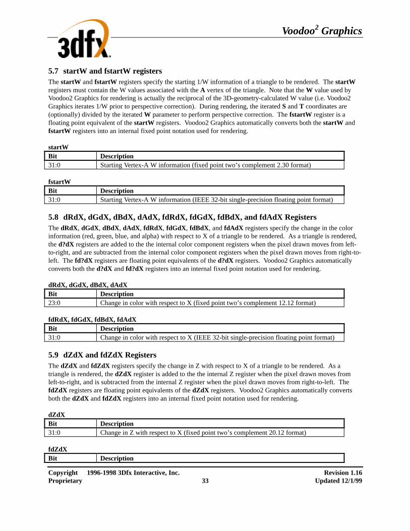
Voodoo2 Graphics
Copyright 1996-1998 3Dfx Interactive, Inc. Revision 1.16 Proprietary 33 Updated 12/1/99
5.7 startW and fstartW registers The startW and fstartW registers specify the starting 1/W information of a triangle to be rendered. The startW registers must contain the W values associated with the A vertex of the triangle. Note that the W value used by Voodoo2 Graphics for rendering is actually the reciprocal of the 3D-geometry-calculated W value (i.e. Voodoo2 Graphics iterates 1/W prior to perspective correction). During rendering, the iterated S and T coordinates are (optionally) divided by the iterated W parameter to perform perspective correction. The fstartW register is a floating point equivalent of the startW registers. Voodoo2 Graphics automatically converts both the startW and fstartW registers into an internal fixed point notation used for rendering. startW Bit Description 31:0 Starting Vertex-A W information (fixed point two’s complement 2.30 format) fstartW Bit Description 31:0 Starting Vertex-A W information (IEEE 32-bit single-precision floating point format)
5.8 dRdX, dGdX, dBdX, dAdX, fdRdX, fdGdX, fdBdX, and fdAdX Registers The dRdX, dGdX, dBdX, dAdX, fdRdX, fdGdX, fdBdX, and fdAdX registers specify the change in the color information (red, green, blue, and alpha) with respect to X of a triangle to be rendered. As a triangle is rendered, the d?dX registers are added to the the internal color component registers when the pixel drawn moves from left-to-right, and are subtracted from the internal color component registers when the pixel drawn moves from right-to-left. The fd?dX registers are floating point equivalents of the d?dX registers. Voodoo2 Graphics automatically converts both the d?dX and fd?dX registers into an internal fixed point notation used for rendering. dRdX, dGdX, dBdX, dAdX Bit Description 23:0 Change in color with respect to X (fixed point two’s complement 12.12 format) fdRdX, fdGdX, fdBdX, fdAdX Bit Description 31:0 Change in color with respect to X (IEEE 32-bit single-precision floating point format)
5.9 dZdX and fdZdX Registers The dZdX and fdZdX registers specify the change in Z with respect to X of a triangle to be rendered. As a triangle is rendered, the dZdX register is added to the the internal Z register when the pixel drawn moves from left-to-right, and is subtracted from the internal Z register when the pixel drawn moves from right-to-left. The fdZdX registers are floating point equivalents of the dZdX registers. Voodoo2 Graphics automatically converts both the dZdX and fdZdX registers into an internal fixed point notation used for rendering. dZdX Bit Description 31:0 Change in Z with respect to X (fixed point two’s complement 20.12 format) fdZdX Bit Description

Voodoo2 Graphics
Copyright 1996-1998 3Dfx Interactive, Inc. Revision 1.16 Proprietary 34 Updated 12/1/99
31:0 Change in Z with respect to X (IEEE 32-bit single-precision floating point format)
5.10 dSdX, dTdX, fdSdX, and fdTdX Registers The dXdX, dTdX, fdSdX, and fdTdX registers specify the change in the S/W and T/W texture coordinates with respect to X of a triangle to be rendered. As a triangle is rendered, the d?dX registers are added to the the internal S and T registers when the pixel drawn moves from left-to-right, and are subtracted from the internal S/W and T/W registers when the pixel drawn moves from right-to-left. Note that the delta S/W and T/W values used by Voodoo2 Graphics for rendering must be divided by W prior to being sent to Voodoo2 Graphics (i.e. Voodoo2 Graphics uses ∆S/W and ∆T/W ). The d?dX registers are floating point equivalents of the fd?dX registers. Voodoo2 Graphics automatically converts both the d?dX and fd?dX registers into an internal fixed point notation used for rendering. dSdX, dTdX Bit Description 31:0 Change in S and T with respect to X (fixed point two’s complement 14.18 format) fdSdX, fdTdX Bit Description 31:0 Change in Z with respect to X (IEEE 32-bit single-precision floating point format)
5.11 dWdX and fdWdX Registers The dWdX and fdWdX registers specify the change in 1/W with respect to X of a triangle to be rendered. As a triangle is rendered, the dWdX register is added to the the internal 1/W register when the pixel drawn moves from left-to-right, and is subtracted from the internal 1/W register when the pixel drawn moves from right-to-left. The fdWdX registers are floating point equivalents of the dWdX registers. Voodoo2 Graphics automatically converts both the dWdX and fdWdX registers into an internal fixed point notation used for rendering. dWdX Bit Description 31:0 Change in W with respect to X (fixed point two’s complement 2.30 format) fdWdX Bit Description 31:0 Change in W with respect to X (IEEE 32-bit single-precision floating point format)
5.12 dRdY, dGdY, dBdY, dAdY, fdRdY, fdGdY, fdBdY, and fdAdY Registers The dRdY, dGdY, dBdY, dAdY, fdRdY, fdGdY, fdBdY, and fdAdY registers specify the change in the color information (red, green, blue, and alpha) with respect to Y of a triangle to be rendered. As a triangle is rendered, the d?dY registers are added to the the internal color component registers when the pixel drawn in a positive Y direction, and are subtracted from the internal color component registers when the pixel drawn moves in a negative Y direction. The fd?dY registers are floating point equivalents of the d?dY registers. Voodoo2 Graphics automatically converts both the d?dY and fd?dY registers into an internal fixed point notation used for rendering. dRdY, dGdY, dBdY, dAdY Bit Description 23:0 Change in color with respect to Y (fixed point two’s complement 12.12 format)

Voodoo2 Graphics
Copyright 1996-1998 3Dfx Interactive, Inc. Revision 1.16 Proprietary 35 Updated 12/1/99
fdRdY, fdGdY, fdBdY, fdAdY Bit Description 31:0 Change in color with respect to Y (IEEE 32-bit single-precision floating point format)
5.13 dZdY and fdZdY Registers The dZdY and fdZdY registers specify the change in Z with respect to Y of a triangle to be rendered. As a triangle is rendered, the dZdY register is added to the the internal Z register when the pixel drawn moves in a positive Y direction, and is subtracted from the internal Z register when the pixel drawn moves in a negative Y direction. The fdZdY registers are floating point equivalents of the dZdY registers. Voodoo2 Graphics automatically converts both the dZdY and fdZdY registers into an internal fixed point notation used for rendering. dZdY Bit Description 31:0 Change in Z with respect to Y (fixed point two’s complement 20.12 format) fdZdY Bit Description 31:0 Change in Z with respect to Y (IEEE 32-bit single-precision floating point format)
5.14 dSdY, dTdY, fdSdY, and fdTdY Registers The dYdY, dTdY, fdSdY, and fdTdY registers specify the change in the S/W and T/W texture coordinates with respect to Y of a triangle to be rendered. As a triangle is rendered, the d?dY registers are added to the the internal S/W and T/W registers when the pixel drawn moves in a positive Y direction, and are subtracted from the internal S/W and T/W registers when the pixel drawn moves in a negative Y direction. Note that the delta S/W and T/W values used by Voodoo2 Graphics for rendering must be divided by W prior to being sent to Voodoo2 Graphics (i.e. Voodoo2 Graphics uses ∆S/W and ∆T/W ). The d?dY registers are floating point equivalents of the fd?dY registers. Voodoo2 Graphics automatically converts both the d?dY and fd?dY registers into an internal fixed point notation used for rendering. dSdY, dTdY Bit Description 31:0 Change in S and T with respect to Y (fixed point two’s complement 14.18 format) fdSdY, fdTdY Bit Description 31:0 Change in Z with respect to Y (IEEE 32-bit single-precision floating point format)
5.15 dWdY and fdWdY Registers The dWdY and fdWdY registers specify the change in 1/W with respect to Y of a triangle to be rendered. As a triangle is rendered, the dWdY register is added to the the internal 1/W register when the pixel drawn moves in a positive Y direction, and is subtracted from the internal 1/W register when the pixel drawn moves in a negative Y direction. The fdWdY registers are floating point equivalents of the dWdY registers. Voodoo2 Graphics automatically converts both the dWdY and fdWdY registers into an internal fixed point notation used for rendering. dWdY Bit Description

Voodoo2 Graphics
Copyright 1996-1998 3Dfx Interactive, Inc. Revision 1.16 Proprietary 36 Updated 12/1/99
31:0 Change in W with respect to Y (fixed point two’s complement 2.30 format) fdWdY Bit Description 31:0 Change in W with respect to Y (IEEE 32-bit single-precision floating point format)
5.16 triangleCMD and ftriangleCMD Registers The triangleCMD and ftriangleCMD registers execute the triangle drawing command. Writes to triangleCMD or ftriangleCMD initiate rendering a triangle defined by the vertex, start, d?dX, and d?dY registers. Note that the vertex, start, d?dX, and d?dY registers must be setup prior to writing to triangleCMD or ftriangleCMD. The value stored to triangleCMD or ftriangleCMD is the area of the triangle being rendered -- this value determines whether a triangle is clockwise or counter-clockwise geometrically. If bit(31)=0, then the triangle is oriented in a counter-clockwise orientation (i.e. positive area). If bit(31)=1, then the triangle is oriented in a clockwise orientation (i.e. negative area). To calculate the area of a triangle, the following steps are performed:
1. The vertices (A, B, and C) are sorted by the Y coordinate in order of increasing Y (i.e. A.y <= B.y <= C.y) 2. The area is calculated as follows: AREA = ((dxAB * dyBC) - (dxBC * dyAB)) / 2 where dxAB = A.x - B.x dyBC = B.y - C.y dxBC = B.x - C.x dyAB = A.y - B.y
Note that Voodoo2 Graphics only requires the sign bit of the area to be stored in the triangleCMD and ftriangleCMD registers -- bits(30:0) written to triangleCMD and ftriangleCMD are ignored. triangleCMD Bit Description 31 Sign of the area of the triangle to be rendered ftriangleCMD Bit Description 31 Sign of the area of the triangle to be rendered (IEEE 32-bit single-precision floating
point format)
5.17 fbzColorPath Register The fbzColorPath register controls the color and alpha rendering pixel pipelines. Bits in fbzColorPath control color/alpha selection and lighting. Individual bits of fbzColorPath are set to enable modulation, addition, etc. for various lighting effects including diffuse and specular highlights. Bit Description 1:0 RGB Select (0=Iterated RGB, 1=Bruce Color Output, 2=Color1 RGB, 3=Reserved) 3:2 Alpha Select (0=Iterated A, 1=Bruce Alpha Output, 2=Color1 Alpha, 3=Reserved) 4 Color Combine Unit control (cc_localselect mux control: 0=iterated RGB, 1=Color0
RGB) 6:5 Alpha Combine Unit control (cca_localselect mux control: 0=iterated alpha, 1=Color0
alpha, 2=clamped iterated Z, 3=clamped iterated W)

Voodoo2 Graphics
Copyright 1996-1998 3Dfx Interactive, Inc. Revision 1.16 Proprietary 37 Updated 12/1/99
7 Color Combine Unit control (cc_localselect_override mux control: 0=cc_localselect, 1=Texture alpha bit(7))
8 Color Combine Unit control (cc_zero_other mux control: 0=c_other, 1=zero) 9 Color Combine Unit control (cc_sub_clocal mux control: 0=zero, 1=c_local) 12:10 Color Combine Unit control (cc_mselect mux control: 0=zero, 1=c_local, 2=a_other,
3=a_local, 4=texture alpha, 5=texture RGB, 6-7=reserved) 13 Color Combine Unit control (cc_reverse_blend control) 14 Color Combine Unit control (cc_add_clocal control) 15 Color Combine Unit control (cc_add_alocal control) 16 Color Combine Unit control (cc_invert_output control) 17 Alpha Combine Unit control (cca_zero_other mux control: 0=a_other, 1=zero) 18 Alpha Combine Unit control (cca_sub_clocal mux control: 0=zero, 1=a_local) 21:19 Alpha Combine Unit control (cca_mselect mux control: 0=zero, 1=a_local, 2=a_other,
3=a_local, 4=texture alpha, 5-7=reserved) 22 Alpha Combine Unit control (cca_reverse_blend control) 23 Alpha Combine Unit control (cca_add_clocal control) 24 Alpha Combine Unit control (cca_add_alocal control) 25 Alpha Combine Unit control (cca_invert_output control) 26 Parameter Adjust (1=adjust parameters for subpixel correction) 27 Enable Texture Mapping (1=enable) 28 Enable RGBA, Z, and W parameter clamping (1=enable) 29 Enable anti-aliasing (1=enable)* (not implemented in Alpha version) Note that the color channels are controlled separately from the alpha channel. There are two primary color selection units: the Color Combine Unit(CCU) and the Alpha Combine Unit (ACU). Bits(1:0), bit(4), and bits(16:8) of fbzColorPath control the Color Combine Unit. The diagram below illustrates the Color Combine Unit controlled by the fbzColorPath register:
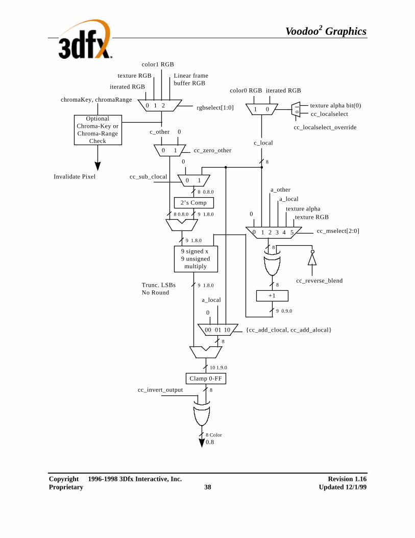
Voodoo2 Graphics
Copyright 1996-1998 3Dfx Interactive, Inc. Revision 1.16 Proprietary 38 Updated 12/1/99
8
9 1.8.0
9 1.8.08 0.8.0
8 Color
10 1.9.0
Clamp 0-FF
8
0.8
cc_invert_output
9 signed x 9 unsigned
multiply
Trunc. LSBsNo Round
9 1.8.0
2’s Comp
c_other
cc_sub_clocal
8 0.8.0
0
0 1
c_local
8
9 0.9.0
+1
8
cc_mselect[2:0]
0
a_local
texture alpha
cc_reverse_blend
{cc_add_clocal, cc_add_alocal}
8
0
00 10
cc_zero_other
0
0 1
a_local
01
iterated RGBcolor0 RGB
OptionalChroma-Key orChroma-Range
Check
chromaKey, chromaRange
Invalidate Pixel
rgbselect[1:0]
texture RGB
iterated RGB
color1 RGB
Linear framebuffer RGB
cc_localselect
a_other
0110 2
0 1 42 3
1 0
texture alpha bit(0)
cc_localselect_override
texture RGB
5

Voodoo2 Graphics
Copyright 1996-1998 3Dfx Interactive, Inc. Revision 1.16 Proprietary 39 Updated 12/1/99
Bits(3:2), bits(6:5), and bits(25:17) of fbzColorPath control the Alpha Combine Unit. The diagram below illustrates the Alpha Combine Unit controlled by the fbzColorPath register:
8
9 1.8.0
9 1.8.08 0.8.0
8 alpha
10 1.9.0
Clamp 0-FF
8
0.8
cca_invert_output
9 signed x 9 unsigned
multiply
Trunc. LSBsNo Round
9 1.8.0
2’s Comp
a_other
cca_sub_clocal
8 0.8.0
0
0 1
a_local
8
9 0.9.0
+1
8
cca_mselect[2:0]
0
cca_reverse_blend
{cca_add_clocal, cca_add_alocal}
8
0
00 10
cca_zero_other
0
0 1
a_local
01
iterated alpha
color0 alpha
aselect[1:0]
texture alpha
iterated alpha
color1 alpha
Linear framebuffer alpha
cca_localselect[1:0]
iterated Z(27:20), clamped
a_local
texture alpha
a_other
10 20 2
0 1 42 3
1
Alpha-MaskCheck
Alpha-Mask Enable3
iterated W(39:32), clamped

Voodoo2 Graphics
Copyright 1996-1998 3Dfx Interactive, Inc. Revision 1.16 Proprietary 40 Updated 12/1/99
Bit(26) of fbzColorPath enables subpixel correction for all parameters. When enabled, Voodoo2 Graphics automatically subpixel corrects the incoming color, depth, and texture coordinate parameters for triangles not aligned on integer spatial boundaries. Enabling subpixel correction decreases the on-chip triangle setup performance from 7 clocks to 16 clocks, but as the triangle setup engine is separately pipelined from the triangle rasterization engine, little if any performance penalty is seen when subpixel correction is enabled. Important Note: When subpixel correction is enabled, the correction is performed on the start registers as they are passed into the triangle setup unit from the PCI FIFO. As a result, the host must pass down new starting parameter information for each new triangle -- if new starting parameter information is not passed down for a new triangle, the starting parameters are subpixel corrected starting with the start registers already subpixel corrected for the last rendered triangle [in effect the parameters are subpixel corrected twice, resulting in inaccuracies in the starting parameter values]. Bit(27) of fbzColorPath is used to enable texture mapping. If texture-mapped rendering is desired, then bit(27) of fbzColorPath must be set. When bit(27)=1, then data is transfered from Bruce to Chuck. If texture mapping is not desired (i.e. Gouraud shading, flat shading, etc.), then bit(27) may be cleared and no data is transfered from Bruce to Chuck. Bit(28) of fbzColorpath is used to enable RGBA, Z, and W parameter clamping. When fbzColorpath bit(28)=1, then the RGBA triangle parameters are be clamped to [0,0xff] inclusive during triangle rasterization. Note that fbzColorpath bit(28) has no effect on the RGBA triangle parameters during triangle setup or sub-pixel correction. When fbzColorpath bit(28)=0, then the RGBA parameters are allowed to wrap according to the following formula:
if(rgbaIterator[23:12] == 0xfff) rgbaClamped[7:0] = 0x0; else if(rgbaIterator[23:12] == 0x100) rgbaClamped[7:0] = 0xff; else rgbaClamped[7:0] = rgbaIterator[19:12];
When fbzColorpath bit(28)=1, then the Z triangle parameter is clamped to [0,0xffff] inclusive during triangle rasterization. Note that fbzColorpath bit(28) has no effect on the Z triangle parameter during triangle setup or sub-pixel correction. Note also that the unclamped Z triangle iterator is used when performing floating point Z-buffering (fbzMode bit(21)=1). When fbzColorpath bit(28)=0, then the Z parameter is allowed to wrap according to the following formula:
if(zIterator[31:12] == 0xfffff) zClamped[15:0] = 0x0; else if(zIterator[31:12] == 0x10000) zClamped[15:0] = 0xffff; else zClamped[15:0] = zIterator[27:12];
When fbzColorpath bit(28)=1, then the W triangle parameter is clamped to [0,0xff] inclusive for use in the Alpha Combine Unit and the fog unit. Note that fbzColorpath bit(28) has no effect on the W triangle parameter during triangle setup or sub-pixel correction. Note also that the unclamped W triangle iterator is used when performing floating point W-buffering (fbzMode bit(21)=0). When fbzColorpath bit(28)=0, then the W parameter used as inputs to the ACU and fog units is allowed to wrap according to the following formula:
if(wIterator[47:32] == 0xffff) wClamped[7:0] = 0x0;

Voodoo2 Graphics
Copyright 1996-1998 3Dfx Interactive, Inc. Revision 1.16 Proprietary 41 Updated 12/1/99
else if(zIterator[47:32] == 0x0100) wClamped[7:0] = 0xff; else wClamped[7:0] = wIterator[39:32];
Bit(29) of fbzColorpath used to enable anti-aliasing. FIXME…
5.18 fogMode Register The fogMode register controls the fog functionality of Voodoo2 Graphics. Bit Description 0 Enable fog (1=enable) 1 Fog Unit control (fogadd control: 0=fogColor, 1=zero) 2 Fog Unit control (fogmult control: 0=Color Combine Unit RGB, 1=zero) 3 Fog Unit control (fogalpha control) 4 Fog Unit control (fogz control) 5 Fog Unit control (fogconstant control: 0=fog multiplier output, 1=fogColor) 6 Fog Unit control (fogdither control, dither the fog blending component) 7 Fog Unit control (fogzones control, enable signed fog delta) The diagram below shows the fog unit of Voodoo2 Graphics:

Voodoo2 Graphics
Copyright 1996-1998 3Dfx Interactive, Inc. Revision 1.16 Proprietary 42 Updated 12/1/99
Color Channel(from Color Combine Unit)
fogmult
0 1
0
fogColor
fogadd0 1
0
9
2’s Comp
8
iterated w(4. 12 floating point)
64x8 RAM(fog alpha)
6 {4 bits exponent, mantissa(11:10)}
64x8 RAM(fog delta alpha)
6 {4 bits exponent, mantissa(11:10)}
8 (.8 format)
89 signed x 9 unsigned multiply
9
8
fogColor
Clamp FF
8 Fogged Color
fogenable
fogenable
1 0
1
mantissa(9:2)8
(6.2 format) 8
8 Color before fog
8 unsigned x 6 unsigned multiply
14 (6.8 format)
2’s Comp11 MSBs (15 truncated)
10
fogzones 11
(6.0 format) 6
1 (0.1format,2nd lsb)
(7.0 format) 74 (0.4 format)
Dither Matrixbit(3)=y [0] xor x [0]bit(2)=y [0]bit(1)=y [1] xor x [1]bit(0)=y [1]
(0.4 format) 4
1 (carry-out)
fogdither
8
fog table alpha
iterated Z(27:20), clamped
0 21 3
iterated alpha
iterated W(39:32), clamped
{fogz, fogalpha}
fogconstant9 (1.8 format)
8 8
carry-in
Bit(0) of fogMode is used to enable fog and atmospheric effects. When fog is enabled, the fog color specified in the fogColor register is blended with the source pixels as a function of the fogTable values and iterated W.

Voodoo2 Graphics
Copyright 1996-1998 3Dfx Interactive, Inc. Revision 1.16 Proprietary 43 Updated 12/1/99
Voodoo2 Graphics supports a 64-entry lookup table (fogTable) to support atmospheric effects such as fog and haze. When enabled, the MSBs of a normalized floating point representation of (1/W) is used to index into the 64-entry fog table. The ouput of the lookup table is an “alpha” value which represents the level of blending to be performed between the static fog/haze color and the incoming pixel color. 8 lower order bits of the floating point (1/W) are used to blend between multiple entries of the lookup table to reduce fog “banding.” The fog lookup table is loaded by the Host CPU, so various fog equations, colors, and effects can be supported. The following table shows the mathematical equations for the supported values of bits(2:1) of fogMode when bits(5:3)=0: Bit(0) - Enable Fog
Bit(1) - fogadd mux control
Bit(2) - fogmult mux control
Fog Equation
0 ignored ignored Cout = Cin 1 0 0 Cout = Afog*Cfog + (1-Afog)*Cin 1 0 1 Cout = Afog*Cfog 1 1 0 Cout = (1-Afog)*Cin 1 1 1 Cout = 0 where: Cout = Color output from Fog block Cin = Color input from Color Combine Unit Module Cfog = fogColor register AFog = alpha value calculated from Fog table Bits(4:3) of fogMode allow other iterators to control the fog alpha. Setting fogMode bits(4:3)=0x1 selects the clamped integer part of the iterated alpha component to be used as the fog alpha instead of the calculated fog alpha from the fog table. Setting fogMode bits(4:3)=0x2 selects the clamped high order integer bits of the iterated Z component to be used as the fog alpha. Setting fogMode bits(4:3)=0x3 selects the clamped low order integer bits of the iterated W component to be used as the fog alpha. Bit(5) of fogMode takes precedence over bits(4:3) and enables a constant value(fogColor) to be added to incoming source color. Bit(6) of fogMode dithers the fog blending factors when for using the fog table. This minimizes fog “banding” visual artifacts . Bit(7) of fogMode allows signed values to be stored in the fog table. This allows fog “zones” to be implemented.
5.19 alphaMode Register The alphaMode register controls the alpha blending and anti-aliasing functionality of Voodoo2 Graphics. Bit Description 0 Enable alpha function (1=enable) 3:1 Alpha function (see table below) 4 Enable alpha blending (1=enable) 7:5 reserved 11:8 Source RGB alpha blending factor (see table below) 15:12 Destination RGB alpha blending factor (see table below) 19:16 Source alpha-channel alpha blending factor (see table below) 23:20 Destination alpha-channel alpha blending factor (see table below) 31:24 Alpha reference value Bits(3:1) specify the alpha function during rendering operations. The alpha function and test pipeline is shown below:
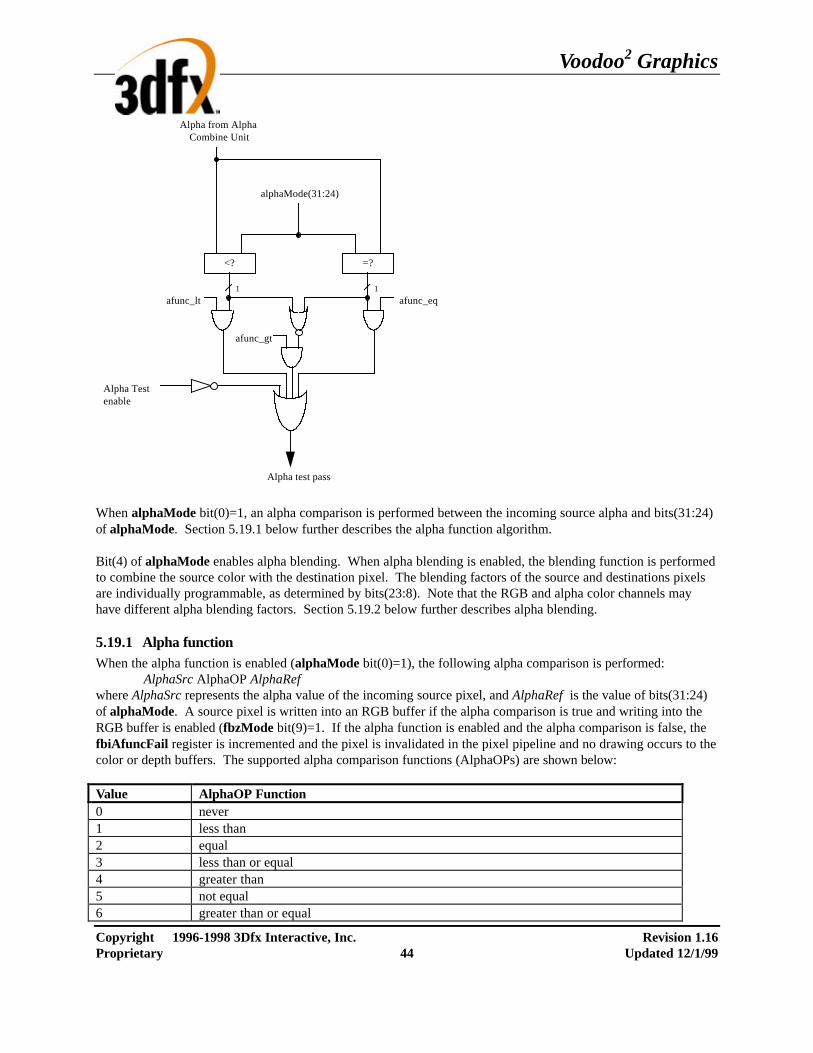
Voodoo2 Graphics
Copyright 1996-1998 3Dfx Interactive, Inc. Revision 1.16 Proprietary 44 Updated 12/1/99
<? =?
1 1
afunc_eqafunc_lt
afunc_gt
Alpha test pass
Alpha Testenable
Alpha from Alpha Combine Unit
alphaMode(31:24)
When alphaMode bit(0)=1, an alpha comparison is performed between the incoming source alpha and bits(31:24) of alphaMode. Section 5.19.1 below further describes the alpha function algorithm. Bit(4) of alphaMode enables alpha blending. When alpha blending is enabled, the blending function is performed to combine the source color with the destination pixel. The blending factors of the source and destinations pixels are individually programmable, as determined by bits(23:8). Note that the RGB and alpha color channels may have different alpha blending factors. Section 5.19.2 below further describes alpha blending.
5.19.1 Alpha function When the alpha function is enabled (alphaMode bit(0)=1), the following alpha comparison is performed: AlphaSrc AlphaOP AlphaRef where AlphaSrc represents the alpha value of the incoming source pixel, and AlphaRef is the value of bits(31:24) of alphaMode. A source pixel is written into an RGB buffer if the alpha comparison is true and writing into the RGB buffer is enabled (fbzMode bit(9)=1. If the alpha function is enabled and the alpha comparison is false, the fbiAfuncFail register is incremented and the pixel is invalidated in the pixel pipeline and no drawing occurs to the color or depth buffers. The supported alpha comparison functions (AlphaOPs) are shown below: Value AlphaOP Function 0 never 1 less than 2 equal 3 less than or equal 4 greater than 5 not equal 6 greater than or equal

Voodoo2 Graphics
Copyright 1996-1998 3Dfx Interactive, Inc. Revision 1.16 Proprietary 45 Updated 12/1/99
7 always
5.19.2 Alpha Blending When alpha blending is enabled (alphaMode bit(4)=1), incoming source pixels are blended with destination pixels. The alpha blending function for the RGB color components is as follows:
Dnew ⇐ (S ⋅ α) + (Dold ⋅ β) where
Dnew The new destination pixel being written into the frame buffer S The new source pixel being generated Dold The old (current) destination pixel about to be modified α The source pixel alpha blending function. β The destination pixel alpha blending function.
The alpha blending function for the alpha components is as follows:
Anew ⇐ (AS ⋅ αd) + (Aold ⋅ βd) where
Anew The new destination alpha being written into the alpha buffer AS The new source alpha being generated Aold The old (current) destination alpha about to be modified αd The source alpha alpha-blending function. βd The destination alpha alpha-blending function.
Note that the source and destination pixels may have different associated alpha blending functions. Also note that RGB color components and the alpha components may have different associated alpha blending functions. The alpha blending factors of the RGB color components are defined in bits(15:8) of alphaMode, while the alpha blending factors of the alpha component is specified in bits(23:16) of alphaMode. The following table lists the alpha blending functions supported for the RGB color components (stored in alphaMode bits(15:8)):
Alpha Blending Function (RGB Color Components)
Alpha Blending Function Pneumonic Alpha Blending Function Description
0x0 AZERO Zero 0x1 ASRC_ALPHA Source alpha 0x2 A_COLOR Color 0x3 ADST_ALPHA Destination alpha 0x4 AONE One 0x5 AOMSRC_ALPHA 1 - Source alpha 0x6 AOM_COLOR 1 - Color 0x7 AOMDST_ALPHA 1 - Destination alpha 0x8-0xe Reserved 0xf (source alpha blending function) ASATURATE MIN(Source alpha, 1 - Destination
alpha) 0xf (destination alpha blending function) A_COLORBEFOREFOG Color before Fog Unit When the value 0x2 is selected as the destination alpha blending factor, the source pixel color is used as the destination blending factor. When the value 0x2 is selected as the source alpha blending factor, the destination pixel color is used as the source blending factor. Note also that the alpha blending function 0xf is different depending upon whether it is being used as a source or destination alpha blending function. When the value 0xf is selected as the destination alpha blending factor, the source color before the fog unit (“unfogged” color) is used as the destination blending factor -- this alpha blending function is useful for multi-pass rendering with atmospheric effects. When the value 0xf is selected as the source alpha blending factor, the alpha-saturate anti-aliasing

Voodoo2 Graphics
Copyright 1996-1998 3Dfx Interactive, Inc. Revision 1.16 Proprietary 46 Updated 12/1/99
algorithm is selected -- this MIN function performs polygonal anti-aliasing for polygons which are drawn in front-to-back order. The following table lists the alpha blending functions supported for the Alpha color component (stored in alphaMode bits(23:16)):
Alpha Blending Function (Alpha Color Component)
Alpha Blending Function Pneumonic Alpha Blending Function Description
0x0 AZERO Zero 0x1-0x3 Reserved 0x4 AONE One 0x5-0xf Reserved
5.20 fbzMode Register The fbzMode register controls frame buffer and depth buffer rendering functions of the Voodoo2 Graphics processor. Bits in fbzMode control clipping, chroma-keying, depth-buffering, dithering, and masking. Bit Description 0 Enable clipping rectangle (1=enable) 1 Enable chroma-keying (1=enable) 2 Enable stipple register masking (1=enable) 3 Floating point depth buffer Select (0=Use integer Z-value for depth buffering, 1=Use
floating point value for depth buffering [either Z or W, controlled by fbzMode bit(21)]) 4 Enable depth-buffering (1=enable) 7:5 Depth-buffer function (see table below) 8 Enable dithering (1=enable) 9 RGB buffer write mask (0=disable writes to RGB buffer) 10 Depth/alpha buffer write mask (0=disable writes to depth/alpha buffer) 11 Dither algorithm (0=4x4 ordered dither, 1=2x2 ordered dither) 12 Enable Stipple pattern masking (1=enable) 13 Enable Alpha-channel mask (1=enable alpha-channel masking) 15:14 Draw buffer (0=Front Buffer, 1=Back Buffer, 2-3=Reserved) 16 Enable depth-biasing (1=enable) 17 Rendering commands Y origin (0=top of screen is origin, 1=bottom of screen is origin) 18 Enable alpha planes (1=enable) 19 Enable alpha-blending dither subtraction (1=enable) 20 Depth buffer source compare select (0=normal operation, 1=zaColor[15:0]) 21 Depth float select (0=iterated W is used for floating point depth buffering, 1=iterated Z
is used for floating point depth buffering) Bit(0) of fbzMode is used to enable the clipping register. When set, clipping to the rectangle defined by the clipLeftRight and clipBottomTop registers inclusive is enabled. When clipping is enabled, the bounding clipping rectangle must always be less than or equal to the screen resolution in order to clip to screen coordinates. Also note that if clipping is not enabled, rendering may not occur outside of the screen resolution. Bit(1) of fbzMode is used to enable the color compare check (chroma-keying). Chroma-keying is enabled by setting fbzMode bit(1)=1 and chromaRange bit(28)=0. When chroma-keying is enabled, any source pixel matching the color specified in the chromaKey register is not written to the RGB buffer. If chroma-ranging is enabled (fbzMode bit(1)=1 and chromaRange bit(28)=1) then any source pixel matching the color criteria controlled by chromaRange bits(27:24)

Voodoo2 Graphics
Copyright 1996-1998 3Dfx Interactive, Inc. Revision 1.16 Proprietary 47 Updated 12/1/99
and specified in the chromaRange and chromaKey registers is not written to theRGB buffer. The chroma-key and chroma-range color compares are performed immediately after texture mapping lookup, but before the color combine unit and fog in the pixel datapath. Bit(2) of fbzMode is used to enable stipple register masking. When enabled, bit(12) of fbzMode is used to determine the stipple mode -- bit(12)=0 specifies stipple rotate mode, while bit(12)=1 specifies stipple pattern mode. When stipple register masking is enabled and stipple rotate mode is selected, bit(31) of the stipple register is used to mask pixels in the pixel pipeline. For all triangle commands and linear frame buffer writes through the pixel pipeline, pixels are invalidated in the pixel pipeline if stipple bit(31)=0 and stipple register masking is enabled in stipple rotate mode. After an individual pixel is processed in the pixel pipeline, the stipple register is rotated from right-to-left, with the value of bit(0) filled with the value of bit(31). Note that the stipple register is rotated regardless of whether stipple masking is enabled (bit(2) in fbzMode) when in stipple rotate mode. When stipple register masking is enabled and stipple pattern mode is selected, the spatial <x,y> coordinates of a pixel processed in the pixel pipeline are used to lookup a 4x8 monochrone pattern stored in the stipple register -- the resultant lookup value is used to mask pixels in the pixel pipeline. For all triangle commands and linear frame buffer writes through the pixel pipeline, a stipple bit is selected from the stipple register as follows: switch(pixel_Y[1:0]) { case 0: stipple_Y_sel[7:0] = stipple[7:0]; case 1: stipple_Y_sel[7:0] = stipple[15:8]; case 2: stipple_Y_sel[7:0] = stipple[23:16]; case 3: stipple_Y_sel[7:0] = stipple[31:24]; } switch(pixel_X[2:0] { case 0: stipple_mask_bit = stipple_Y_sel[7]; case 1: stipple_mask_bit = stipple_Y_sel[6]; case 2: stipple_mask_bit = stipple_Y_sel[5]; case 3: stipple_mask_bit = stipple_Y_sel[4]; case 4: stipple_mask_bit = stipple_Y_sel[3]; case 5: stipple_mask_bit = stipple_Y_sel[2]; case 6: stipple_mask_bit = stipple_Y_sel[1]; case 7: stipple_mask_bit = stipple_Y_sel[0]; } If the stipple_mask_bit=0, the pixel is invalidated in the pixel pipeline when stipple register masking is enabled and stipple pattern mode is selected. Note that when stipple pattern mode is selected the stipple register is never rotated. Bits(4:3) specify the depth-buffering function during rendering operations. The depth buffering pipeline is shown below:

Voodoo2 Graphics
Copyright 1996-1998 3Dfx Interactive, Inc. Revision 1.16 Proprietary 48 Updated 12/1/99
iterated W[47:0], unclamped
wfloat_select1 0
16
iterated Z[27:12], clamped
48 floatSel
16
16 (integer only)
Clamp
zaColor[15:0]zbias_enable
16
<? =?
1 1
old Depth(from Depth Buffer)
zfunc_eqzfunc_lt
zfunc_gt
Depth test pass
Depth Bufferenable
cin wfloat_select
1. Sign extend 16-bit zaColor to 18 bits2. Convert 16-bit depth to 18-bit {underflow,underflow,depth}3. Add 18-bit values4. Clamp to 0-FFFF
wfloat format: 1.<mant> * 2^exp
Clamp
cin = 1
To Fog Unit
4 12
12 mantissaexponent 4
if(|floatSel[47:32]) { mant = 0, exp = 0xf, underflow = 1} else if(!| floatSel[31:16]) { mant = 1, exp = 0xf, underflow = 0} else { exp = find_first_one(floatSel[31:16]) mant = (floatSel[30:16] << exp), underflow = 0}
underflow 1
To adder logic
depthfloat_select1 0
iterated Z[31:0], unclamped
if(|w-iter[47:32]) { mant = 0, exp = 0xf, underflow = 1} else if(!| w-iter[31:16]) { mant = 1, exp = 0xf, underflow = 0} else { exp = find_first_one(w=iter[31:16]) mant = (w-iter[30:16] << exp), underflow = 0}
iterated W[47:0], unclamped
48
4 12
12 mantissaexponent 4
16
treat as 4.28 value, line up decimal points with 16.32 w-term and zero extended to 48 bits
Bit(4) of fbzMode is used to enable depth-buffering. When depth buffering is enabled, a depth comparison is performed for each source pixel as defined in bits(7:5). When bit(3)=0, the z iterator is used for the depth buffer comparison. When bit(3)=1, a floating point representation of either the w iterator or the z iterator is used for the depth buffer comparison. When bit(3)=1 enabling floating point depth-buffering, fbzMode bit(21) selects whether

Voodoo2 Graphics
Copyright 1996-1998 3Dfx Interactive, Inc. Revision 1.16 Proprietary 49 Updated 12/1/99
to use the unclamped w iterator or the unclamped z iterator as the input to the fixed-to-float generation circuitry. When converting from fixed-point format to floating point format, the inverse of the normalized iterator is used for the depth-buffer comparison. This in effect implements a floating-point depth buffering scheme utilizing a 4-bit exponent and a 12-bit mantissa. The inverted mantissa is used so that the same depth buffer comparisons can be used as with a typical integer z-buffer. Section 5.20.1 below further describes the depth-buffering algorithm. Bit(8) of fbzMode enables 16-bit color dithering. When enabled, native 24-bit source pixels are dithered into 16-bit RGB color values with no performance penalty. When dithering is disabled, native 24-bit source pixels are converted into 16-bit RGB color values by bit truncation. When dithering is enabled, bit(11) of fbzMode defines the dithering algorithm -- when bit(11)=0 a 4x4 ordered dither algorithm is used, and when bit(11)=1 a 2x2 ordered dither algorithm is used to convert 24-bit RGB pixels into 16-bit frame buffer colors. Bit(9) of fbzMode enables writes to the RGB buffers. Clearing bit(9) invalidates all writes to the RGB buffers, and thus the RGB buffers remain unmodified for all rendering operations. Bit(9) must be set for normal drawing into the RGB buffers. Similarly, bit(10) enables writes to the depth-buffer. When cleared, writes to the depth-buffer are invalidated, and the depth-buffer state is unmodified for all rendering operations. Bit(10) must be set for normal depth-buffered operation. Bit(13) of fbzMode enables the alpha-channel mask. When enabled, bit(0) of the incoming alpha value is used to mask writes to the color and depth buffers. If alpha channel masking is enabled and bit(0) of the incoming alpha value is 0, then the pixel is invalidated in the pixel pipeline, the fbiAfuncFail register is incremented, and no drawing occurs to the color or depth buffers. If alpha channel masking is enabled and bit(0) of the incoming alpha value is 1, then the pixel is drawn normally subject to depth function, alpha blending function, alpha test, and color/depth masking. Bits(15:14) of fbzMode are used to select the RGB draw buffer for graphics drawing. For typical 3D-rendered applications, drawing is only performed into a back buffer. However, some applications may desire to write into the buffer that is being displayed by the monitor (the front buffer). Bit(16) of fbzMode is used to enable the Depth Buffer bias. When bit(16)=1, the calculated depth value (irrespective of Z or 1/W type of depth buffering selected) is added to bits(15:0) of zaColor. Depth buffer biasing is used to elimate aliasing artifacts when rendering co-planar polygons. Bit(17) of fbzMode is used to define the origin of the Y coordinate for rendering operations (FASTFILL and TRIANGLE commands) and linear frame buffer writes when the pixel pipeline is bypassed for linear frame buffer writes (lfbMode bit(8)=0). Note that bit(17) of fbzMode does not affect linear frame buffer writes when the pixel pipeline is bypassed for linear frame buffer writes (lfbMode bit(8)=0), as in this situation bit(13) of lfbMode specifies the Y origin for linear frame buffer writes. Also note that fbzMode bit(17) is never used to determine the Y origin for linear frame buffer reads, as lfbMode bit(13) always specifies the Y origin for linear frame buffer reads. When cleared, the Y origin (Y=0) for all rendering operations and linear frame buffer writes when the pixel pipeline is enabled is defined to be at the top of the screen. When bit(17) is set, the Y origin is defined to be at the bottom of the screen. Bit(18) of fbzMode is used to enable the destination alpha planes. When set, the auxiliary buffer is used as destination alpha planes. Note that if bit(18) of fbzMode is set that depth buffering cannot be used, and thus bit(4) of fbzMode (enable depth buffering) must be set to 0x0. Bit(19) of fbzMode is used to enable dither subtraction on the destination color during alpha blending. When dither subtraction is enabled (fbzMode bit(19)=1), the dither matrix used to convert 24-bit color to 16-bit color is subtracted from the destination color before applying the alpha-blending algorithm. Enabling dither subtraction is used to enhance image quality when performing alpha-blending.

Voodoo2 Graphics
Copyright 1996-1998 3Dfx Interactive, Inc. Revision 1.16 Proprietary 50 Updated 12/1/99
Bit(20) of fbzMode is used to select the source depth value used for depth buffering. When fbzMode bit(20)=0, the source depth value used for the depth buffer comparison is either iterated Z or iterated W (as selected by fbzMode bit(3)) and may be biased (as controlled by fbzMode bit(16)). When fbzMode bit(20)=1, the constant depth value defined by zaColor[15:0] is used as the source depth value for the depth buffer comparison. Regardless of the state of fbzMode bit(20), the biased iterated Z/W is written into the depth buffer if the depth buffer function passes. Bit(21) of fbzMode is used to select either the w iterator or the z iterator to be used for floating point depth buffering. Floating point depth buffering is enabled when fbzMode bit(4)=1. When fbzMode bit(21)=0, then the unclamped w iterator is converted to a 4.12 floating point representation and used for depth buffering. When fbzMode bit(21)=1, then the unclamped z iterator is converted into a 4.12 floating point format and used for depth buffering.
5.20.1 Depth-buffering function When the depth-buffering is enabled (fbzMode bit(4)=1), the following depth comparison is performed: DEPTHsrc DepthOP DEPTHdst where DEPTHsrc and DEPTHdst represent the depth source and destination values respectively. A source pixel is written into an RGB buffer if the depth comparison is true and writing into the RGB buffer is enabled (fbzMode bit(9)=1). The source depth value is written into the depth buffer if the depth comparison is true and writing into the depth buffer is enabled (fbzMode bit(10)=1). The supported depth comparison functions (DepthOPs) are shown below: Value DepthOP Function 0 never 1 less than 2 equal 3 less than or equal 4 greater than 5 not equal 6 greater than or equal 7 always
5.21 lfbMode Register The lfbMode register controls linear frame buffer accesses. Bit Description 3:0 Linear frame buffer write format (see table below) 5:4 Linear frame buffer write buffer select (0=front buffer, 1=back buffer, 2-3=reserved). 7:6 Linear frame buffer read buffer select (0=front buffer, 1=back buffer, 2=depth/alpha
buffer, 3=reserved). 8 Enable Voodoo2 Graphics pixel pipeline-processed linear frame buffer writes (1=enable) 10:9 Linear frame buffer RGBA lanes (see tables below) 11 16-bit word swap linear frame buffer writes (1=enable) 12 Byte swizzle linear frame buffer writes (1=enable) 13 LFB access Y origin (0=top of screen is origin, 1=bottom of screen is origin) 14 Linear frame buffer write access W select (0=LFB selected, 1=zacolor[15:0]). 15 16-bit word Swap linear frame buffer reads (1=enable)

Voodoo2 Graphics
Copyright 1996-1998 3Dfx Interactive, Inc. Revision 1.16 Proprietary 51 Updated 12/1/99
16 Byte swizzle linear frame buffer reads (1=enable) The following table shows the supported Voodoo2 Graphics linear frame buffer write formats:
Value Linear Frame Buffer Write Format 16-bit formats 0 16-bit RGB (5-6-5) 1 16-bit RGB (x-5-5-5) 2 16-bit ARGB (1-5-5-5) 3 Reserved 32-bit formats 4 24-bit RGB (x-8-8-8) 5 32-bit ARGB (8-8-8-8) 7:6 Reserved 11:8 Reserved 12 16-bit depth, 16-bit RGB (5-6-5) 13 16-bit depth, 16-bit RGB (x-5-5-5) 14 16-bit depth, 16-bit ARGB (1-5-5-5) 15 16-bit depth, 16-bit depth When accessing the linear frame buffer, the cpu accesses information from the starting linear frame buffer (LFB) address space (see section 4 on Voodoo2 Graphics address space) plus an offset which determines the <x,y> coordinates being accessed. Bits(3:0) of lfbMode define the format of linear frame buffer writes. Bits(5:4) of lfbMode select which buffer is written when performing linear frame buffer writes (either front or back buffer). Bits(7:6) of lfbMode select which buffer is read when performing linear frame buffer reads. Note that for linear frame buffer reads, values from the depth/alpha buffer can be read by setting bits(7:6)=0x2. When writing to the linear frame buffer, lfbMode bit(8)=1 specifies that LFB pixels are processed by the normal Voodoo2 Graphics pixel pipeline -- this implies each pixel written must have an associated depth and alpha value, and is also subject to the fog mode, alpha function, etc. If bit(8)=0, pixels written using LFB access bypass the normal Voodoo2 Graphics pixel pipeline and are written to the specified buffer unconditionally and the values written are unconditionally written into the color/depth buffers except for optional color dithering [depth function, alpha blending, alpha test, and color/depth write masks are all bypassed when bit(8)=0]. If bit(8)=0, then only the buffers that are specified in the particular LFB format are updated. Also note that if lfbMode bit(8)=0 that the color and Z mask bits in fbzMode(bits 9 and 10) are ignored for LFB writes. For example, if LFB modes 0-2, or 4 are used and bit(8)=0, then only the color buffers are updated for LFB writes (the depth buffer is unaffected by all LFB writes for these modes, regardless of the status of the Z-mask bit fbzMode bit 10). However, if LFB modes 12-14 are used and bit(8)=0, then both the color and depth buffers are updated with the LFB write data, irrespective of the color and Z mask bits in fbzMode. If LFB mode 15 is used and bit(8)=0, then only the depth buffer is updated for LFB writes (the color buffers are unaffected by all LFB writes in this mode, regardless of the status of the color mask bits in fbzMode). If lfbMode bit(8)=0 and a LFB write format is selected which contains an alpha component (formats 2, 5, and 14) and the alpha buffer is enabled, then the alpha component is written into the alpha buffer. Conversely, if the alpha buffer is not enabled, then the alpha component of LFB writes using formats 2, 5, and 14 when bit(8)=0 are ignored. Note that anytime LFB formats 2, 5, and 14 are used when bit(8)=0 that blending and/or chroma-keying using the alpha component is not performed since the pixel-pipeline is bypassed when bit(8)=0.

Voodoo2 Graphics
Copyright 1996-1998 3Dfx Interactive, Inc. Revision 1.16 Proprietary 52 Updated 12/1/99
If lfbMode bit(8)=0 and LFB write format 14 is used, the component that is ignored is determined by whether the alpha buffer is enabled -- If the alpha buffer is enabled and LFB write format 14 is used with bit(8)=0, then the depth component is ignored for all LFB writes. Conversely, if the alpha buffer is disabled and LFB write format is used with bit(8)=0, then the alpha component is ignored for all LFB writes. If lfbMode bit(8)=1 and a LFB write access format does not include depth or alpha information (formats 0-5), then the appropriate depth and/or alpha information for each pixel written is taken from the zaColor register. Note that if bit(8)=1 that the LFB write pixels are processed by the normal Voodoo2 Graphics pixel pipeline and thus are subject to the per-pixel operations including clipping, dithering, alpha-blending, alpha-testing, depth-testing, chroma-keying, fogging, and color/depth write masking. Bits(10:9) of lfbMode specify the RGB channel format (color lanes) for linear frame buffer writes. The table below shows the Voodoo2 Graphics supported RGB lanes:
Value RGB Channel Format 0 ARGB 1 ABGR 2 RGBA 3 BGRA Bit(11) of lfbMode defines the format of 2 16-bit data types passed with a single 32-bit writes. For linear frame buffer formats 0-2, two 16-bit data transfers can be packed into one 32-bit write -- bit(11) defines which 16-bit shorts correspond to which pixels on screen. The table below shows the pixel packing for packed 32-bit linear frame buffer formats 0-2: lfbMode bit(11) Screen Pixel Packing 0 Right Pixel(host data 31:16), Left Pixel(host data 15:0) 1 Left Pixel(host data 31:16), Right Pixel(host data 15:0) For linear frame buffer formats 12-14, bit(11) of lfbMode defines the bit locations of the 2 16-bit data types passed. The table below shows the data packing for 32-bit linear frame buffer formats 12-14: lfbMode bit(11) Screen Pixel Packing 0 Z value(host data 31:16), RGB value(host data 15:0) 1 RGB value(host data 31:16), Z value(host data 15:0) For linear frame buffer format 15, bit(11) of lfbMode defines the bit locations of the 2 16-bit depth values passed. The table below shows the data packing for 32-bit linear frame buffer format 15: lfbMode bit(11) Screen Pixel Packing 0 Z Right Pixel(host data 31:16), Z Left Pixel(host data 15:0) 1 Z left Pixel(host data 31:16), Z Right Pixel(host data 15:0) Note that bit(11) of lfbMode is ignored for linear frame buffer writes using formats 4 or 5. Bit(12) of lfbMode is used to enable byte swizzling. When byte swizzling is enabled, the 4-bytes within a 32-bit word are swizzled to correct for endian differences between Voodoo2 Graphics and the host CPU. For little endian CPUs (e.g. Intel x86 processors) byte swizzling should not be enabled, however big endian CPUs (e.g. PowerPC processors) should enable byte swizzling. For linear frame buffer writes, the bytes within a word are swizzled prior

Voodoo2 Graphics
Copyright 1996-1998 3Dfx Interactive, Inc. Revision 1.16 Proprietary 53 Updated 12/1/99
to being modified by the other control bits of lfbMode. When byte swizzling is enabled, bits(31:24) are swapped with bits(7:0), and bits(23:16) are swapped with bits(15:8). Note the status of bit(12) of lfbMode has no affect on linear frame buffer reads. Very Important Note: The order of swapping and swizzling operations for LFB writes is as follows: byte swizzling is performed first on all incoming LFB data, as defined by lfbMode bit(12) and irrespective of the LFB data format. After byte swizzling, 16-bit word swapping is performed as defined by lfbMode bit(11). Note that 16-bit word swapping is never performed on LFB data when data formats 4 and 5 are used. Also note that 16-bit word swapping is performed on the LFB data that was previously optionally swapped. Finally, after both swizzling and 16-bit word swapping are performed, the individual color channels are selected as defined in lfbMode bits(10:9). Note that the color channels are selected on the LFB data that was previously swizzled and/or swapped Bit(13) of lfbMode is used to define the origin of the Y coordinate for all linear frame buffer reads and linear frame buffer writes when the pixel pipeline is bypassed (lfbMode bit(8)=0). Note that bit(13) of lfbMode does not affect rendering operations (FASTFILL and TRIANGLE commands) -- bit(17) of fbzMode defines the origin of the Y coordinate for rendering operations. Note also that if the pixel pipeline is enabled for linear frame buffer writes (lfbMode bit(8)=1), then fbzMode bit(17) is used to determine the location of the Y origin. For linear frame buffer reads, however, lfbMode bit(13) is always used to determine the Y origin, regardless of the setting of lfbMode bit(8). When cleared, the Y origin (Y=0) for all linear frame buffer accesses is defined to be at the top of the screen. When bit(13) is set, the Y origin for all linear frame buffer accesses is defined to be at the bottom of the screen. Bit(14) of lfbMode is used to select the W component used for LFB writes processed through the pixel pipeline. If bit(14)=0, then the MSBs of the fractional component of the 48-bit W value passed to the pixel pipeline for LFB writes through the pixel pipeline is the 16-bit Z value associated with the LFB write. [Note that the 16-bit Z value associated with the LFB write is dependent on the LFB format, and is either passed down pixel-by-pixel from the CPU, or is set to the constant zaColor(15:0)]. If bit(14)=1, then the MSBs of the fractional component of the 48-bit W value passed to the pixel pipeline for LFB writes is zacolor(15:0). Regardless of the setting of bit(14), when LFB writes go through the pixel pipeline, all other bits except the 16 MSBs of the fractional component of the W value are set to 0x0. Note that bit(14) is ignored if LFB writes bypass the pixel pipeline.
5.21.1 Linear Frame Buffer Writes Linear frame buffer writes -- format 0: When writing to the linear frame buffer with 16-bit format 0 (RGB 5-6-5), the RGB channel format specifies the RGB ordering within a 16-bit word. If the Voodoo2 Graphics pixel pipeline is enabled for LFB accesses (lfbMode bit(8)=1), then alpha and depth information for LFB format 0 is taken from the zaColor register. The following table shows the color channels for 16-bit linear frame buffer access format 0:
RGB Channel Format Value
16-bit Linear frame buffer access bits
RGB Channel
0 15:0 Red (15:11), Green(10:5), Blue(4:0) 1 15:0 Blue (15:11), Green(10:5), Red(4:0) 2 15:0 Red (15:11), Green(10:5), Blue(4:0) 3 15:0 Blue (15:11), Green(10:5), Red(4:0) Linear frame buffer writes -- format 1: When writing to the linear frame buffer with 16-bit format 1 (RGB 5-5-5), the RGB channel format specifies the RGB ordering within a 16-bit word. If the Voodoo2 Graphics pixel pipeline is enabled for LFB accesses (lfbMode

Voodoo2 Graphics
Copyright 1996-1998 3Dfx Interactive, Inc. Revision 1.16 Proprietary 54 Updated 12/1/99
bit(8)=1), then alpha and depth information for LFB format 1 is taken from the zaColor register. The following table shows the color channels for 16-bit linear frame buffer access format 1:
RGB Channel Format Value
16-bit Linear frame buffer access bits
RGB Channel
0 15:0 Ignored(15), Red (14:10), Green(9:5), Blue(4:0) 1 15:0 Ignored(15), Blue (14:10), Green(9:5), Red(4:0) 2 15:0 Red (15:11), Green(10:6), Blue(5:1), Ignored(0) 3 15:0 Blue (15:11), Green(10:6), Red(5:1), Ignored(0) Linear frame buffer writes -- format 2: When writing to the linear frame buffer with 16-bit format 2 (ARGB 1-5-5-5), the RGB channel format specifies the RGB ordering within a 16-bit word. If the Voodoo2 Graphics pixel pipeline is enabled for LFB accesses (lfbMode bit(8)=1), then depth information for LFB format 2 is taken from the zaColor register. Note that the 1-bit alpha value passed when using LFB format 2 is bit-replicated to yield the 8-bit alpha used in the pixel pipeline. The following table shows the color channels for 16-bit linear frame buffer access format 2:
RGB Channel Format Value
16-bit Linear frame buffer access bits
RGB Channel
0 15:0 Alpha(15), Red (14:10), Green(9:5), Blue(4:0) 1 15:0 Alpha(15), Blue (14:10), Green(9:5), Red(4:0) 2 15:0 Red (15:11), Green(10:6), Blue(5:1), Alpha(0) 3 15:0 Blue (15:11), Green(10:6), Red(5:1), Alpha(0) Linear frame buffer writes -- format 3: Linear frame buffer format 3 is an unsupported format. Linear frame buffer writes -- format 4: When writing to the linear frame buffer with 24-bit format 4 (RGB x-8-8-8), the RGB channel format specifies the RGB ordering within a 24-bit word. Note that the alpha/A channel is ignored for 24-bit access format 4. Also note that while only 24-bits of data is transfered for format 4, all data access must be 32-bit aligned -- packed 24-bit writes are not supported by Voodoo2 Graphics. If the Voodoo2 Graphics pixel pipeline is enabled for LFB accesses (lfbMode bit(8)=1), then alpha and depth information for LFB format 4 is taken from the zaColor register. The following table shows the color channels for 24-bit linear frame buffer access format 4:
RGB Channel Format Value
24-bit Linear frame buffer access bits
(aligned to 32-bits)
RGB Channel
0 31:0 Ignored(31:24), Red (23:16), Green(15:8), Blue(7:0) 1 31:0 Ignored(31:24), Blue(23:16), Green(15:8), Red(7:0) 2 31:0 Red(31:24), Green(23:16), Blue(15:8), Ignored(7:0) 3 31:0 Blue(31:24), Green(23:16), Red(15:8), Ignored(7:0) Linear frame buffer writes -- format 5: When writing to the linear frame buffer with 32-bit format 5 (ARGB 8-8-8-8), the RGB channel format specifies the ARGB ordering within a 32-bit word. If the Voodoo2 Graphics pixel pipeline is enabled for LFB accesses (lfbMode bit(8)=1), then depth information for LFB format 5 is taken from the zaColor register. The following table shows the color channels for 32-bit linear frame buffer access format 5.

Voodoo2 Graphics
Copyright 1996-1998 3Dfx Interactive, Inc. Revision 1.16 Proprietary 55 Updated 12/1/99
RGB Channel Format Value
24-bit Linear frame buffer access bits
(aligned to 32-bits)
RGB Channel
0 31:0 Alpha(31:24), Red (23:16), Green(15:8), Blue(7:0) 1 31:0 Alpha(31:24), Blue(23:16), Green(15:8), Red(7:0) 2 31:0 Red(31:24), Green(23:16), Blue(15:8), Alpha(7:0) 3 31:0 Blue(31:24), Green(23:16), Red(15:8), Alpha(7:0) Linear frame buffer writes -- formats 6-11: Linear frame buffer formats 6-11 are unsupported formats. Linear frame buffer writes -- format 12: When writing to the linear frame buffer with 32-bit format 12 (Depth 16, RGB 5-6-5), the RGB channel format specifies the RGB ordering within the 32-bit word. If the Voodoo2 Graphics pixel pipeline is enabled for LFB accesses (lfbMode bit(8)=1), then alpha information for LFB format 12 is taken from the zaColor register. Note that the format of the depth value passed when using LFB format 12 must precisely match the format of the type of depth buffering being used (either 16-bit integer Z or 16-bit floating point 1/W). The following table shows the 16-bit color channels within the 32-bit linear frame buffer access format 12:
RGB Channel Format Value
16-bit Linear frame buffer access bits
RGB Channel
0 15:0 Red (15:11), Green(10:5), Blue(4:0) 1 15:0 Blue (15:11), Green(10:5), Red(4:0) 2 15:0 Red (15:11), Green(10:5), Blue(4:0) 3 15:0 Blue (15:11), Green(10:5), Red(4:0) Linear frame buffer writes -- format 13: When writing to the linear frame buffer with 32-bit format 13 (Depth 16, RGB x-5-5-5), the RGB channel format specifies the RGB ordering within the 32-bit word. If the Voodoo2 Graphics pixel pipeline is enabled for LFB accesses (lfbMode bit(8)=1), then alpha information for LFB format 13 is taken from the zaColor register. Note that the format of the depth value passed when using LFB format 13 must precisely match the format of the type of depth buffering being used (either 16-bit integer Z or 16-bit floating point 1/W). The following table shows the 16-bit color channels within the 32-bit linear frame buffer access format 13:
RGB Channel Format Value
16-bit Linear frame buffer access bits
RGB Channel
0 15:0 Ignored(15), Red (14:10), Green(9:5), Blue(4:0) 1 15:0 Ignored(15), Blue (14:10), Green(9:5), Red(4:0) 2 15:0 Red (15:11), Green(10:6), Blue(5:1), Ignored(0) 3 15:0 Blue (15:11), Green(10:6), Red(5:1), Ignored(0) Linear frame buffer writes -- format 14: When writing to the linear frame buffer with 32-bit format 14 (Depth 16, ARGB 1-5-5-5), the RGB channel format specifies the RGB ordering within the 32-bit word. Note that the format of the depth value passed when using LFB format 14 must precisely match the format of the type of depth buffering being used (either 16-bit integer Z or 16-bit floating point 1/W). Also note that the 1-bit alpha value passed when using LFB format 14 is bit-replicated to yield the 8-bit alpha used in the pixel pipeline. The following table shows the 16-bit color channels within the 32-bit linear frame buffer access format 14:

Voodoo2 Graphics
Copyright 1996-1998 3Dfx Interactive, Inc. Revision 1.16 Proprietary 56 Updated 12/1/99
RGB Channel Format Value
16-bit Linear frame buffer access bits
RGB Channel
0 15:0 Alpha(15), Red (14:10), Green(9:5), Blue(4:0) 1 15:0 Alpha(15), Blue (14:10), Green(9:5), Red(4:0) 2 15:0 Red (15:11), Green(10:6), Blue(5:1), Alpha(0) 3 15:0 Blue (15:11), Green(10:6), Red(5:1), Alpha(0) Linear frame buffer writes -- format 15: When writing to the linear frame buffer with 32-bit format 15 (Depth 16, Depth 16), the format of the depth values passed must precisely match the format of the type of depth buffering being used (either 16-bit integer Z or 16-bit floating point 1/W). If the Voodoo2 Graphics pixel pipeline is enabled for LFB accesses (lfbMode bit(8)=1), then RGB color information is taken from the color1 register, and alpha information for LFB format 15 is taken from the zaColor register.
5.21.2 Linear Frame Buffer Reads When reading from the linear frame buffer, all data returned is in 16/16 format, with two 16-bit pixels returned for every 32-bit doubleword read. The RGB channel format of the 16-bit pixels read is defined by the rgb channel format field of lfbMode bits(12:9). The alpha/depth buffer can also be read by selecting lfbMode bits(7:6)=0x2. The mapping of the screen space pixels to the two 16-bit words within a 32-bit read are defined by lfbMode bit(15) as shown in the following table: lfbMode bit(15) Screen Pixel Packing 0 Right Pixel(host data 31:16), Left Pixel(host data 15:0) 1 Left Pixel(host data 31:16), Right Pixel(host data 15:0) The value of bit(16) of lfbMode also affects the byte positioning of linear frame buffer reads -- if bit(16)=1, then the LFB read data output from the 16-bit word swap logic is byte-swizzled. Note that byte swizzling (if enabled) is performed after 16-bit word swapping (if enabled) for linear frame buffer reads. Also note that byte swizzling and/or word swapping are performed on reads from the depth/alpha buffer (selected when lfbMode bits(7:6)=0x2) if either or both are enabled. The value of bit(13) of lfbMode selects the position of the Y origin for all linear frame buffer reads. The order of frame buffer read data formatting is illustrated below:

Voodoo2 Graphics
Copyright 1996-1998 3Dfx Interactive, Inc. Revision 1.16 Proprietary 57 Updated 12/1/99
Data from Frame Buffer
64
Color Buffer/Depth Buffer select lfbMode(7:6)
32
Color Lane Select(for colors only) lfbMode(10:9)
32
16-bit Word Swap lfbMode(15)
32
Byte Swizzle lfbMode(16)
32
Data to CPU
See section 9 for more information on linear frame buffer accesses.
5.22 clipLeftRight and clipLowYHighY Registers The clip registers specify a rectangle within which all drawing operations are confined. If a pixel to be drawn lies outside the clip rectangle and clipping is enabled (fbzMode(0)=1), then it is not written into the RGB or depth buffers. Note that the specified clipping rectangle defines a valid drawing area in both the RGB and depth/alpha buffers. The values in the clipping registers are given in pixel units, and the valid drawing rectangle is inclusive of the clipleft and clipLowY register values, but exclusive of the clipRight and clipHighY register values. clipLowY must be less than clipHighY, and clipLeft must be less than clipRight. The clip registers can be enabled by setting bit(0) in the fbzMode register. When clipping is enabled, the bounding clipping rectangle must always be less than or equal to the screen resolution in order to clip to screen coordinates. Also note that if clipping is not enabled, rendering must not be specified to occur outside of the screen resolution. Important Note: The clipLowYHighY register is defined such that y=0 always resides at the top of the monitor screen. Changing the value of the Y origin bits (fbzMode bit(17) or lfbMode bit(13)) has no affect on the clipLowYHighY register orientation. As a result, if the Y origin is defined to be at the bottom of the screen (by setting one of the Y origin bits), care must be taken in setting the clipLowYHighY register to ensure proper functionality. In the case where the Y origin is defined to be at the bottom of the screen, the value of clipLowYHighY is usually set as the number of scan lines in the monitor resolution minus the desired Y clipping values.

Voodoo2 Graphics
Copyright 1996-1998 3Dfx Interactive, Inc. Revision 1.16 Proprietary 58 Updated 12/1/99
The clip registers are also used to define a rectangular region to be drawn during a FASTFILL command. Note that when clipLowYHighY is used to specify a rectangular region for the FASTFILL command, the orientation of the Y origin (top or bottom of the screen) is defined by the status of fbzMode bit(17). See section 7 and the fastfillCMD register description for more information on the FASTFILL command. clipLeftRight Register Bit Description 11:0 Unsigned integer specifying right clipping rectangle edge 15:12 reserved 27:16 Unsigned integer specifying left clipping rectangle edge 31:28 reserved clipLowYHighY Register Bit Description 11:0 Unsigned integer specifying high Y clipping rectangle edge 15:12 reserved 27:16 Unsigned integer specifying low Y clipping rectangle edge 31:28 reserved
5.23 nopCMD Register Writing any data to the nopCMD register executes the NOP command. Executing a NOP command forces completion of all commands and flushes the graphics pipeline, regardless of the data written to nopCMD. Bit 0 of nopCMD is used to optionally clear the fbiPixelsIn, fbiChromaFail, fbiZfuncFail, fbiAfuncFail, and fbiPixelsOut registers. Setting nopCMD bit(0)=1 clears the aforementioned registersl and flushes the graphics pipeline. Setting nopCMD bit(0)=0 does not modify the values of the aforementioned registers but flushes the graphics pipeline. Similarly, setting nopCMD bit(1)=1 clears the fbiTrianglesOut register. Bit Description 0 Clear fbiPixelsIn, fbiChromaFail, fbiZfuncFail, fbiAfuncFail, and fbiPixelsOut
registers (1=clear registers) 1 Clear fbiTrianglesOut register (1=clear register)
5.24 fastfillCMD Register Writing any data to the fastfill register executes the FASTFILL command. The FASTFILL command is used to clear the RGB and depth buffers as quickly as possible. Prior to executing the FASTFILL command, the clipLeftRight and clipLowYHighY are loaded with a rectangular area which is the desired area to be cleared. Note that clip registers define a rectangular area which is inclusive of the clipLeft and clipLowY register values, but exclusive of the clipRight and clipHighY register values. The fastfillCMD register is then written to initiate the FASTFILL command after the clip registers have been loaded. FASTFILL optionally clears the color buffers with the RGB color specified in the color1 register, and also optionally clears the depth buffer with the depth value taken from the zaColor register. Note that since color1 is a 24-bit value, either dithering or bit truncation must be used to translate the 24-bit value into the native 16-bit frame buffer -- dithering may be employed optionally as defined by bit(8) of fbzMode. Disabling clearing of the color or depth buffers is accomplished by modifying the rgb/depth mask bits(10:9) in fbzMode. This allows individual or combined clearing of the RGB and depth buffers.

Voodoo2 Graphics
Copyright 1996-1998 3Dfx Interactive, Inc. Revision 1.16 Proprietary 59 Updated 12/1/99
5.25 swapbufferCMD Register Writing to the swapbufferCMD register executes the SWAPBUFFER command: Bit Description 0 Synchronize frame buffer swapping to vertical retrace (1=enable) 8:1 Swap buffer interval 9 Disable buffer swapping (1=do not swap buffers) If the data written to swapbufferCMD bit(0)=0, then the frame buffer swapping is not synchronized with vertical retrace. If frame buffer swapping is not synchronized with vertical retrace, then visible frame “tearing” may occur. If swapbufferCMD bit(0)=1 then the frame buffer swapping is synchronized with vertical retrace. Synchronizing frame buffer swapping with vertical retrace eliminates the aforementioned frame “tearing.” When a swapbufferCMD is received in the front-end PCI host FIFO, the swap buffers pending field in the status register is incremented. Conversely, when an actual frame buffer swapping occurs, the swap buffers pending field in the status register (bits(30:28)) is decremented. The swap buffers pending field allows software to determine how many SWAPBUFFER commands are present in the Voodoo2 Graphics FIFOs. Bits(8:1) of swapbufferCMD are used to specify the number of vertical retraces to wait before swapping the color buffers. An internal counter is incremented whenever a vertical retrace occurs, and the color buffers are not swapped until the internal vertical retrace counter is greater than the value of swapbufferCMD bits(8:1) -- After a swap occurs, the internal vertical retrace counter is cleared. Specifying values other than zero for bits(8:1) are used to maintain constant frame rate. Note that if vertical retrace synchronization is disabled for swapping buffers (swapbufferCMD(0)=0), then the swap buffer interval field is ignored. When triple buffering is enabled (fbiInit2(4)=1), three color buffers are used to improve overall rendering performance. When triple buffering is enabled and a SWAPBUFFER command is executed, Voodoo2 Graphics begins rendering into a third buffer instead of waiting for vertical retrace. Since time is not spent waiting for vertical retrace to occur, overall rendering performance is improved. But similar to when only two color buffers are used, Voodoo2 Graphics only changes the front buffer pointer during active vertical retrace (to eliminate visual tearing). If rendering to the third buffer has completed before the first SWAPBUFFER command has changed the front buffer pointer and a new SWAPBUFFER command is executed, then the hardware automatically waits for vertical retrace before continuing execution – this allows up to 2 fully-rendered buffers to be queued and waiting to be displayed when using triple buffering. Note that syncing to vertical retrace must be enabled and the swapbuffer interval must be 0x0 when using triple buffering (swapbufferCMD(8:0=0x1). Bit 9 of swapbufferCMD is used to disable swapping of the front and back buffer pointers for the SWAPBUFFER command. Normally, bit 9 of swapbufferCMD is set to 0 and the front and back buffer pointers are swapped upon execution of a SWAPBUFFER command. However, simultaneously setting bits 0 and 9 of swapbufferCMD allows an application to force the hardware to wait for vertical retrace before continuing execution, but without actually swapping buffers. Note that bit 9 of swapbufferCMD must be 0 when using triple buffering.
5.26 fogColor Register The fogColor register is used to specify the fog color for fogging operations. Fog is enabled by setting bit(0) in fogMode. See the fogMode and fogTable register descriptions for more information fog. Bit Description 7:0 Fog Color Blue 15:8 Fog Color Green

Voodoo2 Graphics
Copyright 1996-1998 3Dfx Interactive, Inc. Revision 1.16 Proprietary 60 Updated 12/1/99
23:16 Fog Color Red 31:24 reserved
5.27 zaColor Register The zaColor register is used to specify constant alpha and depth values for linear frame buffer writes, FASTFILL commands, and co-planar polygon rendering support. For certain linear frame buffer access formats, the alpha and depth values associated with a pixel written are the values specified in zaColor. See the lfbMode register description for more information. When executing the FASTFILL command, the constant 16-bit depth value written into the depth buffer is taken from bits(15:0) of zaColor. When fbzMode bit(16)=1 enabling depth-biasing, the constant depth value required is taken from zaColor bits(15:0). Bit Description 15:0 Constant Depth 23:16 reserved 31:24 Constant Alpha
5.28 chromaKey Register The chromaKey register is used for chroma-keying and chroma-ranging operations. For chroma-keying, the chromaKey register specifies a color which is compared with all pixels to be written into the RGB buffer. If a color match is detected between an outgoing pixel and the chromaKey register, and chroma-keying is enabled (fbzMode bit(1)=1 and chromaRange bit(28)=0), then the pixel is not written into the frame buffer. An outgoing pixel is still written into the RGB buffer if chroma-keying/ranging is disabled or the chromaKey color does not equal the outgoing pixel color. For chroma-ranging, the chromaKey register specifies the lower limit color for the chroma-range operation. Chroma-ranging is enabled by setting fbzMode bit(1)=1 and chromaRange bit(28)=1. See the chromaRange register description for more information on chroma-ranging functionality. Note that the alpha color component of an outgoing pixel is ignored in the chroma-key and chroma-range color compare circuits. The chroma-key and chroma-range comparisons are performed immediately after texture lookup, but before lighting, fog, or alpha blending. See the description of the fbzColorPath register for further information on the location of the chroma-key and chroma-range comparison circuitry. The format of chromaKey is a 24-bit RGB color. Bit Description 7:0 Chroma-key Blue 15:8 Chroma-key Green 23:16 Chroma-key Red 31:24 reserved
5.29 chromaRange Register The chromaRange register specifies a 24-bit RGB color value which is compared to all pixels to be written to the color buffer. If chroma-keying is enabled (fbzMode[1]) and chroma-ranging is enabled (chromaRange[28]), the outgoing pixel color is compared to a color range formed by the colors of the chromaKey and chromaRange registers.
Each RGB color component of the chromaKey and chromaRange registers defines a chroma range for the color component The color component range includes the lower limit color from the chromaKey register and the upper
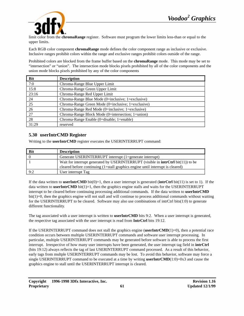
Voodoo2 Graphics
Copyright 1996-1998 3Dfx Interactive, Inc. Revision 1.16 Proprietary 61 Updated 12/1/99
limit color from the chromaRange register. Software must program the lower limits less-than or equal to the upper limits.
Each RGB color component chromaRange mode defines the color component range as inclusive or exclusive. Inclusive ranges prohibit colors within the range and exclusive ranges prohibit colors outside of the range.
Prohibited colors are blocked from the frame buffer based on the chromaRange mode. This mode may be set to “intersection” or “union”. The intersection mode blocks pixels prohibited by all of the color components and the union mode blocks pixels prohibited by any of the color components
Bit Description 7:0 Chroma-Range Blue Upper Limit 15:8 Chroma-Range Green Upper Limit 23:16 Chroma-Range Red Upper Limit 24 Chroma-Range Blue Mode (0=inclusive; 1=exclusive) 25 Chroma-Range Green Mode (0=inclusive; 1=exclusive) 26 Chroma-Range Red Mode (0=inclusive; 1=exclusive) 27 Chroma-Range Block Mode (0=intersection; 1=union) 28 Chroma-Range Enable (0=disable; 1=enable) 31:29 reserved
5.30 userIntrCMD Register Writing to the userIntrCMD register executes the USERINTERRUPT command: Bit Description 0 Generate USERINTERRUPT interrupt (1=generate interrupt) 1 Wait for interrupt generated by USERINTERRUPT (visible in intrCtrl bit(11)) to be
cleared before continuing (1=stall graphics engine until interrupt is cleared) 9:2 User interrupt Tag If the data written to userIntrCMD bit(0)=1, then a user interrupt is generated (intrCtrl bit(11) is set to 1). If the data written to userIntrCMD bit(1)=1, then the graphics engine stalls and waits for the USERINTERRUPT interrupt to be cleared before continuing processing additional commands. If the data written to userIntrCMD bit(1)=0, then the graphics engine will not stall and will continue to process additional commands without waiting for the USERINTERRUPT to be cleared. Software may also use combinations of intrCtrl bits(1:0) to generate different functionality. The tag associated with a user interrupt is written to userIntrCMD bits 9:2. When a user interrupt is generated, the respective tag associated with the user interrupt is read from IntrCtrl bits 19:12. If the USERINTERRUPT command does not stall the graphics engine (userIntrCMD(1)=0), then a potential race condition occurs between multiple USERINTERRUPT commands and software user interrupt processing. In particular, multiple USERINTERRUPT commands may be generated before software is able to process the first interrupt. Irrespective of how many user interrupts have been generated, the user interrupt tag field in intrCtrl (bits 19:12) always reflects the tag of last USERINTERRUPT command processed. As a result of this behavior, early tags from multple USERINTERRUPT commands may be lost. To avoid this behavior, software may force a single USERINTERRUPT command to be executed at a time by writing userIntrCMD(1:0)=0x3 and cause the graphics engine to stall until the USERINTERRUPT interrupt is cleared.

Voodoo2 Graphics
Copyright 1996-1998 3Dfx Interactive, Inc. Revision 1.16 Proprietary 62 Updated 12/1/99
Note that bit 5 of intrCtrl must be set to 1 for user interrupts to be generated – writes to userIntrCMD when intrCtrl(5)=0 do not generate interrupts or cause the processing of commands to wait on clearing of the USERINTERRUPT command (regardless of the data written to userIntrCMD), and are thus in effect “dropped.”
5.31 stipple Register The stipple register specifies a mask which is used to enable individual pixel writes to the RGB and depth buffers. See the stipple functionality description in the fbzMode register description for more information. Bit Description 31:0 stipple value
5.32 color0 Register The color0 register specifies constant color values which are used for certain rendering functions. In particular, bits(23:0) of color0 are optionally used as the c_local input in the color combine unit. In addition, bits(31:24) of color0 are optionally used as the c_local input in the alpha combine unit. See the fbzColorPath register description for more information. Bit Description 7:0 Constant Color Blue 15:8 Constant Color Green 23:16 Constant Color Red 31:24 Constant Color Alpha
5.33 color1 Register The color1 register specifies constant color values which are used for certain rendering functions. In particular, bits(23:0) of color1 are optionally used as the c_other input in the color combine unit selected by bits(1:0) of fbzColorPath. The alpha component of color1(bits(31:24)) are optionally used as the a_other input in the alpha combine unit selected by bits(3:2) of fbzColorPath. The color1 register bits(23:0) are also used by the FASTFILL command as the constant color for screen clears. Also, for linear frame buffer write format 15(16-bit depth, 16-bit depth), the color for the pixel pipeline is taken from color1 if the pixel pipeline is enabled for linear frame buffer writes (lfbMode bit(8)=1). Bit Description 7:0 Constant Color Blue 15:8 Constant Color Green 23:16 Constant Color Red 31:24 Constant Color Alpha
5.34 fbiTrianglesOut Register The fbiTriangles register is a 24-bit counter which is incremented for each triangle processed by the Voodoo2 Graphics triangle walking engine. Triangles which are backface culled in the triangle setup unit do not increment fbiTrianglesOut. fbiTrianglesOut is reset to 0x0 on power-up reset, and is also reset to 0x0 when a ‘1’ is written to nopCMD bit(1). Bit Description 23:0 Rendered triangles (total number of triangles rendered by the Voodoo2 Graphics
triangle rendering engine)

Voodoo2 Graphics
Copyright 1996-1998 3Dfx Interactive, Inc. Revision 1.16 Proprietary 63 Updated 12/1/99
5.35 fbiPixelsIn Register The fbiPixelsIn register is a 24-bit counter which is incremented for each pixel processed by the Voodoo2 Graphics triangle walking engine. fbiPixelsIn is incremented irrespective if the triangle pixel is actually drawn or not as a result of the depth test, alpha test, etc. fbiPixelsIn is used primarily for statistical information, and in essence allows software to count the number of pixels in a screen-space triangle. fbiPixelsIn is reset to 0x0 on power-up reset, and is also reset to 0x0 when a ‘1’ is written to nopCMD bit(0). Bit Description 23:0 Pixel Counter (number of pixels processed by Voodoo2 Graphics triangle engine)
5.36 fbiChromaFail Register The fbiChromaFail register is a 24-bit counter which is incremented each time an incoming source pixel (either from the triangle engine or linear frame buffer writes through the pixel pipeline) is invalidated in the pixel pipeline because of the chroma-key color match test. If an incoming source pixel color matches the chomaKey register, fbiChromaFail is incremented. fbiChromaFail is reset to 0x0 on power-up reset, and is also reset to 0x0 when a ‘1’ is written to nopCMD bit(0). Bit Description 23:0 Pixel Counter (number of pixels failed chroma-key test)
5.37 fbiZfuncFail Register The fbiZfuncFail register is a 24-bit counter which is incremented each time an incoming source pixel (either from the triangle engine or linear frame buffer writes through the pixel pipeline) is invalidated in the pixel pipeline because of a failure in the Z test. The Z test is defined and enabled in the fbzMode register. fbiZfuncFail is reset to 0x0 on power-up reset, and is also reset to 0x0 when a ‘1’ is written to nopCMD bit(0). Bit Description 23:0 Pixel Counter (number of pixels failed Z test)
5.38 fbiAfuncFail Register The fbiAfuncFail register is a 24-bit counter which is incremented each time an incoming source pixel (either from the triangle engine or linear frame buffer writes through the pixel pipeline) is invalidated in the pixel pipeline because of a failure in the alpha test. The alpha test is defined and enabled in the alphaMode register. The fbiAfuncFail register is also incremented if an incoming source pixel is invalidated in the pixel pipeline as a result of the alpha masking test (bit(13) in fbzMode). fbiAfuncFail is reset to 0x0 on power-up reset, and is also reset to 0x0 when a ‘1’ is written to nopCMD bit(0). Bit Description 23:0 Pixel Counter (number of pixels failed Alpha test)
5.39 fbiPixelsOut Register The fbiPixelsOut register is a 24-bit counter which is incremented each time a pixel is written into a color buffer during rendering operations (rendering operations include triangle commands, linear frame buffer writes, and the FASTFILL command). Pixels tracked by fbiPixelsOut are therefore subject to the chroma-test, Z test, Alpha test, etc. that are part of the regular Voodoo2 Graphics pixel pipeline. fbiPixelsOut is used to count the number of

Voodoo2 Graphics
Copyright 1996-1998 3Dfx Interactive, Inc. Revision 1.16 Proprietary 64 Updated 12/1/99
pixels actually drawn (as opposed to the number of pixels processed counted by fbiPixelsIn). Note that the RGB mask (fbzMode bit(9) is ignored when determining fbiPixelsOut. fbiPixelsOut is reset to 0x0 on power-up reset, and is also reset to 0x0 when a ‘1’ is written to nopCMD bit(0). Bit Description 23:0 Pixel Counter (number of pixels drawn to color buffer)
5.40 fbiSwapHistory Register The fbiSwapHistory register keeps track of the number of vertical syncs which occur between executed swap commands. fbiSwapHistory logs this information for the last 8 executed swap commands. Upon completion of a swap command, fbiSwapHistory bits (27:0) are shifted left by four bits to form the new fbiSwapHistory bits (31:4), which maintains a history of the number of vertical syncs between execution of each swap command for the last 7 frames. Then, fbiSwapHistory bits(3:0) are updated with the number of vertical syncs which occurred between the last swap command and the just completed swap command or the value 0xf, whichever is less. Bit Description 3:0 Number of vertical syncs between the second most recently completed swap command
and the most recently completed swap command, or the value 0xf, whichever is less for Frame N.
7:4 Vertical sync swapbuffer history for Frame N-1 11:8 Vertical sync swapbuffer history for Frame N-2 15:12 Vertical sync swapbuffer history for Frame N-3 19:16 Vertical sync swapbuffer history for Frame N-4 23:20 Vertical sync swapbuffer history for Frame N-5 27:24 Vertical sync swapbuffer history for Frame N-6 31:28 Vertical sync swapbuffer history for Frame N-7
5.41 fogTable Register The fogTable register is used to implement fog functions in Voodoo2 Graphics. The fogTable register is a 64-entry lookup table consisting of 8-bit fog blending factors and 8-bit ∆fog blending values. The ∆fog blending values are the difference between successive fog blending factors in fogTable and are used to blend between fogTable entries. Note that the ∆fog blending factors are stored in 6.2 format, while the fog blending factors are stored in 8.0 format. For most applications, the 6.2 format ∆fog blending factors have the two LSBs set to 0x0, with the six MSBs representing the difference between successive fog blending factors. Also note that as a result of the 6.2 format for the ∆fog blending factors, the difference between successive fog blending factors cannot exceed 63. When storing the fog blending factors, the sum of each fog blending factor and ∆fog blending factor pair must not exceed 255. When loading fogTable, two fog table entries must be written concurrently in a 32-bit word. A total of 32 32-bit PCI writes are required to load the entire fogTable register. fogTable[n] (0 ≤ n ≤ 31) Bit Description 7:0 FogTable[2n] ∆Fog blending factor 15:8 FogTable[2n] Fog blending factor 23:16 FogTable[2n+1] ∆Fog blending factor 31:24 FogTable[2n+1] Fog blending factor

Voodoo2 Graphics
Copyright 1996-1998 3Dfx Interactive, Inc. Revision 1.16 Proprietary 65 Updated 12/1/99
5.42 vRetrace Register The vRetrace register is used to determine the position of the monitor vertical refresh beam. The vRetrace register allows software to read the status of the internal vSyncOff counter used for vertical video timing. The vRetrace register allows an application to determine the amount of time before the next vertical sync. Note that vRetrace is read only. Also note that the value of vRetrace is 0x0 when vertical sync is active, which is determined by bit(6) of the status register. vRetrace is provided for software compatibility with Voodoo Graphics, but it is suggested that the hvRetrace register be used instead to simultaneously query the status of both the horizontal and vertical refresh beams. See section 13 for more information on video timing. Bit Description 12:0 internal vSyncOff counter value (read only)
5.43 hvRetrace Register The hvRetrace register is used to determine the position of the monitor horizontal and vertical refresh beams. Bits (12:0) of hvRetrace are used to allow software to read the status of the internal vSyncOff counter used for vertical video timing. hvRetrace bits(12:0) allow an application to determine the amount of time before the next vertical sync. Note that the value of hvRetrace bits(12:0) is 0x0 when vertical sync is active, which is determined by bit(6) of the status register Bits (26:16) of hvRetrace are used to allow software to determine the horizontal refresh beam position. Horizontal sync is active (i.e. the horizontal refresh beam is being pulled back towards the left edge of the monitor) when hvRetrace bits(26:16) are less than the value of the hSyncOn field of the hSync register (bits (8:0)). Horizontal sync is inactive (i.e. valid data is being displayed on the monitor) when hvRetrace bits(26:16) are greater than the value of the hSyncOn field of the hSync register. The following psuedo-code illustrates the functionality of the hRetrace counter value:
hSyncOn = GET(hSync_Register) & 0x1ff; hBackporch = GET(backPorch_Register) & 0x1ff; xDimensioin = GET(videoDimensions_Register) & 0x7ff; hRetrace = (GET(hvRetrace_Register) >> 16) & 0x7ff; if(hRetrace < hSyncOn) // Horizontal Sync is active… else if((hRetrace < (hSyncOn + hBackPorch)) || (hRetrace >= (hSyncOn + hBackPorch + xDimension))) // Horizontal Sync is inactive, but within horizontal blanking else XpixelBeingDisplayed = hRetrace - hSyncOn - hBackporch;
If syncing reads from hvRetrace is enabled (fbiinit5 bit(15)=1), then reading from hvRetrace will cause a full handshake to occur between the PCI controller and the video control unit to guarantee valid, stable values are returned to software. See section 13 for more information on video timing. Bit Description 12:0 internal vSyncOff counter value (read only) 15:13 reserved 26:16 internal hRetrace counter value (read only)
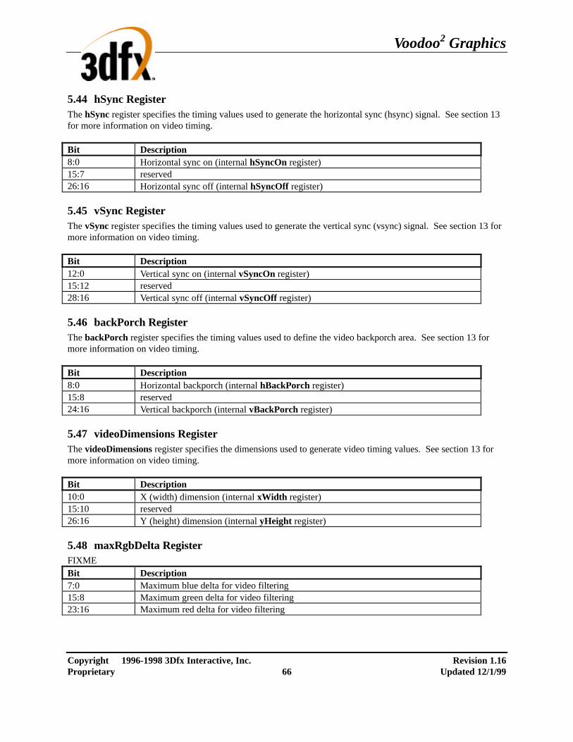
Voodoo2 Graphics
Copyright 1996-1998 3Dfx Interactive, Inc. Revision 1.16 Proprietary 66 Updated 12/1/99
5.44 hSync Register The hSync register specifies the timing values used to generate the horizontal sync (hsync) signal. See section 13 for more information on video timing. Bit Description 8:0 Horizontal sync on (internal hSyncOn register) 15:7 reserved 26:16 Horizontal sync off (internal hSyncOff register)
5.45 vSync Register The vSync register specifies the timing values used to generate the vertical sync (vsync) signal. See section 13 for more information on video timing. Bit Description 12:0 Vertical sync on (internal vSyncOn register) 15:12 reserved 28:16 Vertical sync off (internal vSyncOff register)
5.46 backPorch Register The backPorch register specifies the timing values used to define the video backporch area. See section 13 for more information on video timing. Bit Description 8:0 Horizontal backporch (internal hBackPorch register) 15:8 reserved 24:16 Vertical backporch (internal vBackPorch register)
5.47 videoDimensions Register The videoDimensions register specifies the dimensions used to generate video timing values. See section 13 for more information on video timing. Bit Description 10:0 X (width) dimension (internal xWidth register) 15:10 reserved 26:16 Y (height) dimension (internal yHeight register)
5.48 maxRgbDelta Register FIXME Bit Description 7:0 Maximum blue delta for video filtering 15:8 Maximum green delta for video filtering 23:16 Maximum red delta for video filtering

Voodoo2 Graphics
Copyright 1996-1998 3Dfx Interactive, Inc. Revision 1.16 Proprietary 67 Updated 12/1/99
5.49 hBorder Register The hBorder register specifies the timing values used to generate the horizontal border color area. See section 13 for more information on video timing. Bit Description 8:0 Horizontal backporch border color (internal hBackColor register) 15:7 reserved 24:16 Horizontal frontporch border color (internal hFrontColor register)
5.50 vBorder Register The vBorder register specifies the timing values used to generate the vertical border color area. See section 13 for more information on video timing. Bit Description 8:0 Vertical backporch border color (internal vBackColor register) 15:7 reserved 24:16 Vertical frontporch border color (internal vFrontColor register)
5.51 borderColor Register The borderColor register specifies the color value output in the border color area. See section 13 for more information on video timing. Bit Description 7:0 Video border color (blue) 15:8 Video border color (green) 23:16 Video border color (red)
5.52 fbiInit0 Register The fbiInit0 register is used for hardware initialization and configuration of the Chuck chip. Writes to fbiInit0 are ignored unless PCI configuration register initWrEnable bit(0)=1. Writes to fbiInit0 are not put into the PCI bus FIFO and are written immediately, so care must be taken when writing to fbiInit0 if data is in the PCI bus FIFO or the graphics engine is busy. Also, writes to fbiInit registers must not occur within a PCI burst, as all writes to fbiInit registers must be single cycle writes only. Bit Description Miscellaneous Control 0 VGA passthrough (controls external pins vga_pass and vga_pass_n). Default value is
the value of fb_addr_a[4] at the deassertion of pci_rst 1 Chuck Graphics Reset (0=run, 1=reset). Default is 0. 2 Chuck FIFO Reset (0=run, 1=reset). Default is 0. [resets PCI FIFO and the PCI data
packer] 3 Byte swizzle incoming register writes (1=enable). [Register byte data is swizzled if
fbiInit0[3]=1 and pci_address[20]=1]. Default is 0. FIFO Control

Voodoo2 Graphics
Copyright 1996-1998 3Dfx Interactive, Inc. Revision 1.16 Proprietary 68 Updated 12/1/99
4 Stall PCI enable for High Water Mark (0=disable, 1=enable). Default is 1. 5 reserved 10:6 PCI FIFO Empty Entries Low Water Mark. Valid values are 0-31. Default is 0x10. 11 Linear frame buffer accesses stored in memory FIFO (1=enable). Default is 0. 12 Texture memory accesses stored in memory FIFO (1=enable). Default is 0. 13 Memory FIFO enable (0=disable, 1=enable). Default is 0. 24:14 Memory FIFO High Water Mark (bits [15:5]). Default is 0x0. 30:25 Memory FIFO Write Burst High Water Mark (Range 0-63 -- must be greater than
fbiinit4[7:2]). Default is 0x0. 31 reserved
5.53 fbiInit1 Register The fbiInit1 register is used for hardware initialization and configuration of the Chuck chip. Writes to fbiInit1 are ignored unless PCI configuration register initWrEnable bit(0)=1. Writes to fbiInit1 are not put into the PCI bus FIFO and are written immediately, so care must be taken when writing to fbiInit1 if data is in the PCI bus FIFO or the graphics engine is busy. Also, writes to fbiInit registers must not occur within a PCI burst, as all writes to fbiInit registers must be single cycle writes only. Bit Description PCI Bus Controller Configuration 0 PCI Device Function Number (0=pass-thru Voodoo2 Graphics only, 1=combo board
with VGA dev #0 and Voodoo2 Graphics dev#1). Default value is the value of fb_addr_a[3] at the deassertion of pci_rst. Read only.
1 Wait state cycles for PCI write accesses (0=no ws, 1=one ws). Default is 1. 2 Reserved. Hardwired to 0. Read only. (old multi-CVG configuration detect) 3 Enable linear frame buffer reads (1=enable). Default is 0. This bit is included so that
Voodoo2 Graphics potentially won’t hang the system during random reads during powerup.
Video Controller Configuration (1) 7:4 Number of 32x32 video tiles in X/Horizontal dimension (bits 4:1). Default is 0x0. The
6-bit number of tiles in the X dimension is formed by {fbiInit1[24], fbiInit1[7:4], fbiInit6[30]}.
8 Video Timing Reset (0=run, 1=reset). Default is 1. 9 Software override of HSYNC/VSYNC (0=normal operation, 1=software override).
Default is 0. 10 Software override HSYNC value. Default is 0. 11 Software override VSYNC value. Default is 0. 12 Software blanking enable (0=normal operation, 1=Always blank monitor). Default is 1. 13 Drive video timing data outputs (0=tristate, 1=drive outputs). Default is 0. 14 Drive video timing blank output (0=tristate, 1=drive output). Default is 0. 15 Drive video timing hsync/vsync outputs (0=tristate, 1=drive outputs). Default is 0. 16 Drive video timing dclk output (0=tristate, 1=drive output). Default is 0. 17 Video timing vclk input select (0=vid_clk_2x, 1=vid_clk_slave, 2=dac_data[16]). Input
select is {fbiInit5[13], fbiInit1[17]}. Default is 0. 19:18 Vid_clk_2x delay select (0=no delay, 1=4 ns, 2=6 ns, 3=8 ns). Default is 0. 21:20 Video timing vclk source select (0=vid_clk_slave, 1=vid_clk_2x [divided by 2],
2,3=vid_clk_2x_sel). Default is 2.

Voodoo2 Graphics
Copyright 1996-1998 3Dfx Interactive, Inc. Revision 1.16 Proprietary 69 Updated 12/1/99
22 Enable 24 Bits-per-pixel video output (1=enable). Default is 0. 23 Enable scan-line interleaving (1=enable). Default is 0. 24 Number of 32x32 video tiles in X/Horizontal dimension (bit 5). Default is 0x0. The 6-
bit number of tiles in the X dimension is formed by {fbiInit1[24], fbiInit1[7:4], fbiInit6[30]}.
25 Enable video edge detection filtering (1=enable). Default is 0. 26 Invert vid_clk_2x (0=pass-thru vid_clk_2x, 1=invert vid_clk_2x). Default is 0. 28:27 Vid_clk_2x_sel delay select (0=no delay, 1=4 ns, 2=6 ns, 3=8 ns). Default is 0. 30:29 Vid_clk delay select (0=no delay, 1=4 ns, 2=6 ns, 3=8 ns). Default is 0. 31 Disable fast Read-Ahead-Write to Read-Ahead-Read turnaround (1=disable). Default is
0.
5.54 fbiInit2 Register The fbiInit2 register is used for hardware initialization and configuration of the Chuck chip. Writes to fbiInit2 are ignored unless PCI configuration register initWrEnable bit(0)=1. Writes to fbiInit2 are not put into the PCI bus FIFO and are written immediately, so care must be taken when writing to fbiInit2 if data is in the PCI bus FIFO or the graphics engine is busy. Also, writes to fbiInit registers must not occur within a PCI burst, as all writes to fbiInit registers must be single cycle writes only. Bit Description DRAM Memory Controller Configuration 0 Disable video dither subtraction (1=disable). Default is 0x0. 1 DRAM banking configuration (0=128Kx16 banking, 1=256Kx16 banking) 3:2 reserved 4 Triple Buffering Enable (1=enable). Default is 0x0. Bit included for binary
compatibility with Voodoo Graphics only. Use fbiInit5[10:9] for buffer memory allocation.
5 Enable fast RAS read cycles [bring RAS high early on reads] (1=enable). Default is 0x0.
6 Enable generated dram OE signal (1=enable). Default is 0x1. 7 Enable fast Read-Ahead -Write turnaround [bit(6) must be set]. (1=enable). Default is
0x0. 8 Enable pass-through dither mode [For 8 BPP apps only] (1=enable). Default is 0x0. 10:9 Swap buffer algorithm (0=based on dac_vsync, 1=based on dac_data[0], 2=based on
pci_fifo_stall, 3=based on sli_syncin/sli_syncout). Default is 0x0. Video/DRAM Controller Configuration (2) 19:11 Video Buffer Offset (=150 for 640x480, =247 for 832x608). Default is 0x0. 20 Enable DRAM banking (1=enable). Default is 0. 21 Enable DRAM Read Ahead FIFO (1=enable). Default is 0x0. DRAM Refresh Control 22 Refresh Enable (0=disable, 1=enable). Default is 0. 31:23 Refresh_Load Value. (Internal 14-bit counter 5 LSBs are 0x0). Default is 0x100.

Voodoo2 Graphics
Copyright 1996-1998 3Dfx Interactive, Inc. Revision 1.16 Proprietary 70 Updated 12/1/99
5.55 fbiInit3 Register The fbiInit3 register is used for hardware initialization and configuration of the Chuck chip. Writes to fbiInit3 are ignored unless PCI configuration register initWrEnable bit(0)=1. Writes to fbiInit3 are not put into the PCI bus FIFO and are written immediately, so care must be taken when writing to fbiInit3 if data is in the PCI bus FIFO or the graphics engine is busy. Also, writes to fbiInit registers must not occur within a PCI burst, as all writes to fbiInit registers must be single cycle writes only. Bit Description Miscellaneous Control 0 Triangle register address remapping (0=use normal register mapping, 1=use aliased
register mapping). [Alternate register mapping is used when fbiInit3(0)=1 and pci_address[21]=1]. Default is 0x0.
5:1 Video FIFO threshold. Default is 0x0. 6 Disable Texture Mapping (0=normal, 1=disable Trex-to-Chuck Interface). Default is
0x0. 7 reserved Chuck power-on configuration bits 10:8 Generic power-on strapping pins. Default value is the value of fb_addr_a[2:0] at the
deassertion of pci_rst. Read only 11 VGA_PASS reset value. Default value is the value of fb_addr_a[4] at the deassertion of
pci_rst. Read only 12 Hardcode PCI base address 0x10000000 (1=enable, 0=normal operation). Default value
is the value of fb_addr_a[5] at the deassertion of pci_rst Bruce interface configuration bits 16:13 fbi-to-trex bus clock delay selections (0-15). Default is 0x2. 21:17 trex-to-fbi bus FIFO full threshold (0-31). Default is 0xf. Y Origin Definition bits 31:22 Y Origin Swap subtraction value (10 bits). Default is 0x0.
5.56 fbiInit4 Register The fbiInit4 register is used for hardware initialization and configuration of the Chuck chip. Writes to fbiInit4 are ignored unless PCI configuration register initWrEnable bit(0)=1. Writes to fbiInit4 are not put into the PCI bus FIFO and are written immediately, so care must be taken when writing to fbiInit4 if data is in the PCI bus FIFO or the graphics engine is busy. Also, writes to fbiInit registers must not occur within a PCI burst, as all writes to fbiInit registers must be single cycle writes only. Bit Description Miscellaneous Control 0 Wait state cycles for PCI read accesses (0=1 ws, 1=2 ws). Default is 1. 1 Enable Read-ahead logic for linear frame buffer reads (1=enable). Default is 0. 7:2 Memory FIFO low water mark for PCI FIFO. [Dump PCI FIFO contents to memory if
PCI FIFO freespace falls below this level]. Default is 0.

Voodoo2 Graphics
Copyright 1996-1998 3Dfx Interactive, Inc. Revision 1.16 Proprietary 71 Updated 12/1/99
17:8 Memory FIFO row start (base row address for beginning of memory FIFO). Default is 0.
27:18 Memory FIFO row rollover (row value when FIFO counters rollover). Default is 0. 29 reserved 31:29 Video clocking delay control (Chuck revision 5 only). Default is 0.
5.57 fbiInit5 Register The fbiInit5 register is used for hardware initialization and configuration of the Chuck chip. Writes to fbiInit5 are ignored unless PCI configuration register initWrEnable bit(0)=1. Writes to fbiInit5 are not put into the PCI bus FIFO and are written immediately, so care must be taken when writing to fbiInit5 if data is in the PCI bus FIFO or the graphics engine is busy. Also, writes to fbiInit registers must not occur within a PCI burst, as all writes to fbiInit registers must be single cycle writes only. Bit Description Chuck power-on configuration bits 0 Disable pci_stop functionality (0=normal operation, 1=disable pci_stop). Default value
is the value of fb_addr_b[0] at the deassertion of pci_rst. 1 PCI Slave device is 66 MHz capable (0=33 MHz capable, 1=66 MHz capable). Default
value is the value of fb_addr_b[1] at the deassertion of pci_rst. Read only. 2 dac_data output width (0=16-bit, 1=24-bit). Default value is the value of fb_addr_b[2]
at the deassertion of pci_rst. Read only. 3 dac_data[17]/GPIO_0 output value (dac_data[17] is only driven when
fb_addr_b[2]=0 at the deassertion of pci_rst). Default value is the value of fb_addr_b[3] at the deassertion of pci_rst.
4 dac_data[18]/GPIO_1 control. (dac_data[18] is only driven when fb_addr_b[2]=0 at the deassertion of pci_rst). GPIO_1 is controlled by fbiInit5[4] and fbiInit5[27]. When fbiInit5[27]=0, then GPIO_1 is driven with the input value of dac_data[23]/GPIO_3. When fbiInit5[27]=1, then GPIO_1 is driven with the value specified by fbiInit5[4]. Default value of fbiInit5[4] is the value of fb_addr_b[4] at the deassertion of pci_rst.
8:5 Generic power-on strapping pins. Default value is the value of fb_addr_b[8:5] at the deassertion of pci_rst. Read only
Miscellaneous Control 10:9 Color/Aux buffer memory allocation (0=2 color buffers/1 aux buffer, 1=3 color buffers/0
aux buffers, 2=3 color buffers/1 aux buffer, 3=reserved). Default is 0x0. 11 Drive vid_clk_slave output (0=tristate, 1=drive output). Default is 0. 12 Drive dac_data[16] output (0=tristate, 1=drive output). Do not set to 1 when 24-bit dac
data output is enabled (fbiInit5[25]=1). 13 Video timing vclk input select (0=vid_clk_2x, 1=vid_clk_slave, 2=dac_data[16]). Input
select is {fbiInit5[13], fbiInit1[17]}. Default is 0. 14 Multi-CVG configuration detect (0=one Voodoo2 Graphics configuration, 1=two
Voodoo2 Graphics configuration). Default value is the value of sli_syncin at the deassertion of pci_rst. Read only.
15 Synchronize reads from hRetrace and vRetrace registers across video clock boundry (1=enable). Default is 0.
16 Horizontal border color enable, right edge (1=enable). Default is 0. 17 Horizontal border color enable, left edge (1=enable). Default is 0.
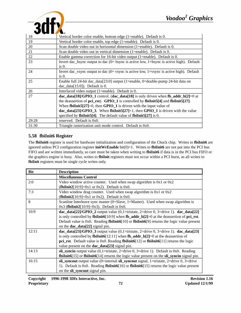
Voodoo2 Graphics
Copyright 1996-1998 3Dfx Interactive, Inc. Revision 1.16 Proprietary 72 Updated 12/1/99
18 Vertical border color enable, bottom edge (1=enable). Default is 0. 19 Vertical border color enable, top edge (1=enable). Default is 0. 20 Scan double video out in horizontal dimension (1=enable). Default is 0. 21 Scan double video out in vertical dimension (1=enable). Default is 0. 22 Enable gamma correction for 16-bit video output (1=enable). Default is 0. 23 Invert dac_hsync output to dac (0= hsync is active low, 1=hsync is active high). Default
is 0. 24 Invert dac_vsync output to dac (0= vsync is active low, 1=vsync is active high). Default
is 0. 25 Enable full 24-bit dac_data[23:0] output (1=enable, 0=double-pump 24-bit data on
dac_data[15:0]). Default is 0. 26 Interlaced video output (1=enable). Default is 0. 27 dac_data[18]/GPIO_1 control. (dac_data[18] is only driven when fb_addr_b[2]=0 at
the deassertion of pci_rst). GPIO_1 is controlled by fbiInit5[4] and fbiInit5[27]. When fbiInit5[27]=0, then GPIO_1 is driven with the input value of dac_data[23]/GPIO_3. When fbiInit5[27]=1, then GPIO_1 is driven with the value specified by fbiInit5[4]. The default value of fbiInit5[27] is 0.
29:28 reserved. Default is 0x0. 31:30 Triangle rasterization unit mode control. Default is 0x0.
5.58 fbiInit6 Register The fbiInit6 register is used for hardware initialization and configuration of the Chuck chip. Writes to fbiInit6 are ignored unless PCI configuration register initWrEnable bit(0)=1. Writes to fbiInit6 are not put into the PCI bus FIFO and are written immediately, so care must be taken when writing to fbiInit6 if data is in the PCI bus FIFO or the graphics engine is busy. Also, writes to fbiInit registers must not occur within a PCI burst, as all writes to fbiInit registers must be single cycle writes only. Bit Description Miscellaneous Control 2:0 Video window active counter. Used when swap algorithm is 0x1 or 0x2
(fbiInit2[10:9]=0x1 or 0x2). Default is 0x0. 7:3 Video window drag counter. Used when swap algorithm is 0x1 or 0x2
(fbiInit2[10:9]=0x1 or 0x2). Default is 0x0. 8 Scanline Interleave sync master (0=Slave, 1=Master). Used when swap algorithm is
0x3 (fbiInit2[10:9]=0x3). Default is 0x0. 10:9 dac_data[22]/GPIO_2 output value (0,1=tristate, 2=drive 0, 3=drive 1). dac_data[22]
is only controlled by fbiInit6[10:9] when fb_addr_b[2]=0 at the deassertion of pci_rst. Default value is 0x0. Reading fbiInit6[10] or fbiInit6[9] returns the logic value present on the dac_data[22] signal pin.
12:11 dac_data[23]/GPIO_3 output value (0,1=tristate, 2=drive 0, 3=drive 1). dac_data[23] is only controlled by fbiInit6[12:11] when fb_addr_b[2]=0 at the deassertion of pci_rst. Default value is 0x0. Reading fbiInit6[12] or fbiInit6[11] returns the logic value present on the dac_data[23] signal pin.
14:13 sli_syncin output value (0,1=tristate, 2=drive 0, 3=drive 1). Default is 0x0. Reading fbiInit6[15] or fbiInit6[14] returns the logic value present on the sli_syncin signal pin.
16:15 sli_syncout output value (0=internal sli_syncout signal, 1=tristate, 2=drive 0, 3=drive 1). Default is 0x0. Reading fbiInit6[16] or fbiInit6[15] returns the logic value present on the sli_syncout signal pin.

Voodoo2 Graphics
Copyright 1996-1998 3Dfx Interactive, Inc. Revision 1.16 Proprietary 73 Updated 12/1/99
18:17 dac_rd output value (0=internal dac_rd signal, 1=tristate, 2=drive 0, 3=drive 1). Default is 0x0. Reading fbiInit6[18] or fbiInit6[17] returns the logic value present on the dac_rd signal pin.
20:19 dac_wr output value (0=internal dac_wr signal, 1=tristate, 2=drive 0, 3=drive 1). Default is 0x0. Reading fbiInit6[20] or fbiInit6[19] returns the logic value present on the dac_wr signal pin.
27:21 PCI FIFO Empty Entries Low Water Mark used to generate pci_fifo_rdy_n (output on dac_data[21]). Valid values are 0-64. Default is 0x0.
29:28 vga_pass_n output value (0,1=internal vga_pass_n signal, 2=drive 0, 3=drive 1). Default is 0x0. vga_pass_n is only driven when fb_addr_b[2]=0 at the deassertion of pci_rst).
30 Number of 32x32 video tiles in the X/Horizontal dimension (bit 0). Default is 0x0. The 6-bit number of tiles in the X dimension is formed by {fbiInit1[24], fbiInit1[7:4], fbiInit6[30]}.
31 reserved
5.59 fbiInit7 Register The fbiInit7 register is used for hardware initialization and configuration of the Chuck chip. Writes to fbiInit7 are ignored unless PCI configuration register initWrEnable bit(0)=1. Writes to fbiInit7 are not put into the PCI bus FIFO and are written immediately, so care must be taken when writing to fbiInit7 if data is in the PCI bus FIFO or the graphics engine is busy. Also, writes to fbiInit registers must not occur within a PCI burst, as all writes to fbiInit registers must be single cycle writes only. Bit Description Miscellaneous Control 7:0 Generic power-on strapping pins. Default value is the value of fb_data[63:56] at the
deassertion of pci_rst. Read only 8 CMDFIFO enable (1=enable). Default is 0. Note: fbiinit7 bit(8) is mutually exclusive
with fbiinit0 bit(13) (memory FIFO enable). 9 CMDFIFO offscreen memory store (0=execute CMDFIFO stream out of internal FIFOs
only, 1=execute CMDFIFO using offscreen memory). Default is 0. 10 Disable internal CMDFIFO hole counting logic (1=disable). Default is 0. If set,
requires software to manually “bump” the CMDFIFO depth with writes to the cmdFifoDepth register
15:11 CMDFIFO read fetch threshold (range 0-31). Default is 0. 16 Synchronize writes to CMDFIFO registers across graphics clock boundry (1=enable).
Default is 0. 17 Synchronize reads from CMDFIFO registers across graphics clock boundry (1=enable).
Default is 0. 18 Reset PCI packer (0=normal operation, 1=reset PCI packer). Default is 0. 19 Enable chromaKey and chromaRange writes to Bruce (1=enable). Default is 0. 26:20 CMDFIFO PCI timeout counter value (range 0-127). Default is 0x0. 27 Enable bursting of consecutive texture memory writes across FT Bus (1=enable).
Default is 0.

Voodoo2 Graphics
Copyright 1996-1998 3Dfx Interactive, Inc. Revision 1.16 Proprietary 74 Updated 12/1/99
5.60 cmdFifoBaseAddr Register The cmdFifoBaseAddr register is used to control the hardware CMDFIFO. cmdFifoBaseAddr is used to store the starting page (or row address) and the ending page of where the CMDFIFO is stored in physical memory. Writes to cmdFifo registers must not occur within a PCI burst, as all writes to cmdFifo registers must be single cycle writes only. Bit Description 9:0 CMDFIFO base address, specified in pages (row address). Default is 0x0. 15:10 reserved 25:16 CMDFIFO end address, specified in pages (row address). Default is 0x0.
5.61 cmdFifoBump Register The cmdFifoBump register accesses the internal CMDFIFO bump register. Writes to cmdFifo registers must not occur within a PCI burst, as all writes to cmdFifo registers must be single cycle writes only. Bit Description 15:0 Internal CMDFIFO bump register
5.62 cmdFifoRdPtr Register The cmdFifoRdPtr register accesses the internal CMDFIFO read pointer. Writes to cmdFifo registers must not occur within a PCI burst, as all writes to cmdFifo registers must be single cycle writes only. Bit Description 31:0 Internal CMDFIFO read pointer
5.63 cmdFifoAMin Register The cmdFifoAMin register accesses the internal CMDFIFO minimum address register. Writes to cmdFifo registers must not occur within a PCI burst, as all writes to cmdFifo registers must be single cycle writes only. Bit Description 31:0 Internal CMDFIFO minimum address register
5.64 cmdFifoAMax Register The cmdFifoAMax register accesses the internal CMDFIFO maximum address register. Writes to cmdFifo registers must not occur within a PCI burst, as all writes to cmdFifo registers must be single cycle writes only. Bit Description 31:0 Internal CMDFIFO maximum address register
5.65 cmdFifoDepth Register The cmdFifoDepth register accesses the internal CMDFIFO depth register. Writes to cmdFifo registers must not occur within a PCI burst, as all writes to cmdFifo registers must be single cycle writes only. Bit Description

Voodoo2 Graphics
Copyright 1996-1998 3Dfx Interactive, Inc. Revision 1.16 Proprietary 75 Updated 12/1/99
15:0 Internal CMDFIFO depth register
5.66 cmdFifoHoles Register The cmdFifoHoles register accesses the internal CMDFIFO number of holes register. Writes to cmdFifo registers must not occur within a PCI burst, as all writes to cmdFifo registers must be single cycle writes only. Bit Description 15:0 Internal CMDFIFO number of holes register
5.67 clutData Register The clutData register is used the load values into the internal video Color Lookup table used for video gamma correction. Bit Description 7:0 Blue color component to be written to video Color Lookup Table 15:8 Green color component to be written to video Color Lookup Table 23:16 Red color component to be written to video Color Lookup Table 29:24 Index of video Color Lookup Table to be written (Range 0-32 only). The Chuck internal Color Lookup table is used for gamma correction of 16-bit RGB values during video refresh. The 16-bit RGB values read from the frame buffer are used to index into the internal video Color Lookup table. The output of the video Color Lookup table is then fed to an external DAC. The video Color Lookup Table is stored internally as a 33x24 RAM. As RGB values are input from memory, the 5 MSBs of a particular color channel are used to index into the Color Lookup Table. The 3 LSBs of a particular color channel are then used to linearly interpolate between multiple video Color Lookup Table entries. As a result of the linear interpolation performed, smooth transitions from one Color Lookup Table index to surrounding indices results. Using linear interpolation, a much smaller video Color Lookup Table (33 entries) can be used instead of a full Color Lookup Table (256 entries). As a result of the linear interpolation, however, all entries stored in the videoColor Lookup Table must be monotonically increasing. To modify an entry in the Color Lookup Table, writes are performed to the clutData register. The index of the Color Lookup Table entry to be modified is stored in the data passed to the clutData register. Important Note: When writingto clutData to modify the contents of the video Color Lookup Table, the video unit must be running (fbiInit1(8)=0). Writing to clutData when the video unit is reset (fbiInit1(8)=1) will result in undefined behavior.
5.68 dacData Register The dacData register provides a means to writing to the registers of the external DAC. Bit Description 7:0 External DAC register write data 10:8 External DAC register address, bits(2:0) 11 External DAC read command (1=read external DAC, 0=write external DAC) 13:12 External DAC register address, bits(4:3)

Voodoo2 Graphics
Copyright 1996-1998 3Dfx Interactive, Inc. Revision 1.16 Proprietary 76 Updated 12/1/99
Reads and writes to the external DAC are only allowed when the memory bus is idle, as the external DAC register bus is time-multiplexed with the memory data lines. Thus, software must guarantee that there are no conflicts between the memory controller and external DAC accesses. This can be accomplished in two ways: (1) resetting the video control unit (fbiinit1 bit(8)=1), flushing the pixel pipeline with a NOP command, and waiting for the graphics subsystem to be idle (status(9)=1), or (2) waiting for VSYNC to be active, flushing the pixel pipeline, and waiting for the graphics subsystem to be idle. Once there are no internal resources requesting the memory controller, accesses to the external DAC can be safely performed. Writes to the external DAC are performed by writing the dacData register with bits(7:0) specifying the register data, bits (13:12, 10:8) specifying the register address, and bit(11) cleared to 0. Bit(11) of dacData must be cleared to 0 when performing external DAC writes. Reads from the external DAC are performed by writing to the dacData register with the register address specified in bits (13:12, 10:8) and bit(11) set to 1. Bit(11) of dacData must be set to 1 when performing external DAC reads. The data read from the External DAC is stored in an internal register of Chuck, and is read by setting bit(2) in the PCI Configuration register initEnable and reading from the fbiinit2 register. When fbiinit2/fbiinit3 address remapping is enabled (PCI Configuration register initEnable bit(2)=1), reading from fbiinit2 bits (7:0) returns the last value read from the external DAC (fbiinit2 bits(31:8) are undefined when address remapping is enabled). Note that reading from the external DAC is a two-step process: first the read is initiated by writing to the dacData register with bit(11) set to 1; then the read data is read by the CPU by reading from fbinit2 bits(7:0) with fbiinit2/fbinit3 address remapping is enabled. FIXME – what are registers for internal RAMDAC, PLLs, and NTSC/ENCODER??
5.69 sSetupMode Register The sSetupMode register provides a way for the CPU to only setup required parameters. When a Bit is set, that parameter will be calculated in the setup process, otherwise the value is not passed down to the triangle, and the previous value will be used. Also the definition of the triangle strip is defined in bits 19:16, where bit 16 defines fan. Culling is enabled by seting bit 17 to a value of “1”, whereas bit 18 defines the culling sign. Bit 19 disables the ping pong sign inversion that happens during triangle strips.
Bit Description 0 Setup Red, Green, and Blue 1 Setup Alpha 2 Setup Z 3 Setup Wb 4 Setup W0 5 Setup S0 and T0 6 Setup W1 7 Setup S1 and T1 15:8 reserved 16 Strip mode (0=strip, 1=fan) 17 Enable Culling (0=disable, 1=enable) 18 Culling Sign (0=positive sign, 1=negative sign) 19 Disable ping pong sign correction during triangle strips (0=normal, 1=disable)
5.70 Triangle Setup Vertex Registers The sVx, sVy registers specify the x and y coordinates of a triangle strip to be rendered. A triangle strip, once the initial triangle has been defined, only requires a new X and Y to render consecutive triangles. The diagram below illustrates how triangle strips are sent over to Voodoo2 Graphics:
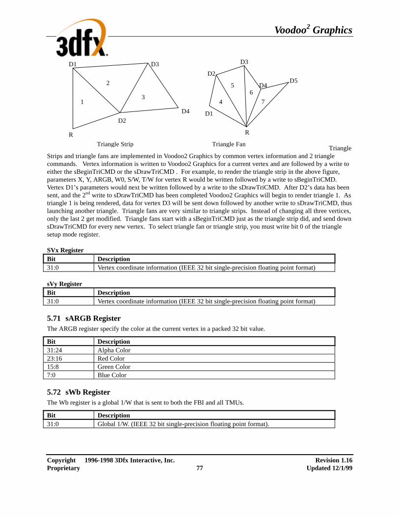
Voodoo2 Graphics
Copyright 1996-1998 3Dfx Interactive, Inc. Revision 1.16 Proprietary 77 Updated 12/1/99
R
D1
D2
D3
D4
R
D1
D2
D3
D4D5
Triangle Strip Triangle Fan
1
2
34
56
7
Triangle Strips and triangle fans are implemented in Voodoo2 Graphics by common vertex information and 2 triangle commands. Vertex information is written to Voodoo2 Graphics for a current vertex and are followed by a write to either the sBeginTriCMD or the sDrawTriCMD . For example, to render the triangle strip in the above figure, parameters X, Y, ARGB, W0, S/W, T/W for vertex R would be written followed by a write to sBeginTriCMD. Vertex D1’s parameters would next be written followed by a write to the sDrawTriCMD. After D2’s data has been sent, and the 2nd write to sDrawTriCMD has been completed Voodoo2 Graphics will begin to render triangle 1. As triangle 1 is being rendered, data for vertex D3 will be sent down followed by another write to sDrawTriCMD, thus launching another triangle. Triangle fans are very similar to triangle strips. Instead of changing all three vertices, only the last 2 get modified. Triangle fans start with a sBeginTriCMD just as the triangle strip did, and send down sDrawTriCMD for every new vertex. To select triangle fan or triangle strip, you must write bit 0 of the triangle setup mode register. SVx Register Bit Description 31:0 Vertex coordinate information (IEEE 32 bit single-precision floating point format) sVy Register Bit Description 31:0 Vertex coordinate information (IEEE 32 bit single-precision floating point format)
5.71 sARGB Register The ARGB register specify the color at the current vertex in a packed 32 bit value.
Bit Description 31:24 Alpha Color 23:16 Red Color 15:8 Green Color 7:0 Blue Color
5.72 sWb Register The Wb register is a global 1/W that is sent to both the FBI and all TMUs.
Bit Description 31:0 Global 1/W. (IEEE 32 bit single-precision floating point format).
Voodoo2 Graphics
Copyright 1996-1998 3Dfx Interactive, Inc. Revision 1.16 Proprietary 78 Updated 12/1/99
5.73 sS/W0 Register The S/W0 register is the S coordinate of the current vertex divided by W, for all TMUs.
Bit Description 31:0 Texture S coordinate (IEEE 32 bit single-precision floating point format)
5.74 sT/W0 Register The T/W register s the T coordinate of the current vertex divided by W, for all TMUs.
Bit Description 31:0 Texture T coordinate (IEEE 32 bit single-precision floating point format)
5.75 sVz Register The Vz register is the Z value at the current vertex.
Bit Description 31:0 Vertex coordinate information (IEEE 32 bit single-precision floating point format)
5.76 sWtmu0 Register The sWtmu0 register is all the TMUs local 1/W value for the current vertex.
Bit Description 31:0 Texture local 1/W. (IEEE 32 bit single-precision floating point format)
5.77 sWtmu1 Register The sWtmu1 register is TMU1’s local 1/W value for the current vertex.
Bit Description 31:0 Texture local 1/W. (IEEE 32 bit single-precision floating point format)
5.78 sS/Wtmu1 Register The sS/Wtmu1 register is TMU1’s local S/W value for the current vertex.
Bit Description 31:0 Texture local 1/W. (IEEE 32 bit single-precision floating point format)
5.79 sT/Wtmu1 Register The sT/Wtmu1 register is TMU1’s local T/W value for the current vertex.
Bit Description 31:0 Texture local 1/W. (IEEE 32 bit single-precision floating point format)
5.80 sAlpha Register the sAlpha register is the separated alpha value for the current vertex.
Bit Description 31:0 Alpha value at vertex (0.0 - 255.0). (IEEE 32 bit single-precision floating point format)

Voodoo2 Graphics
Copyright 1996-1998 3Dfx Interactive, Inc. Revision 1.16 Proprietary 79 Updated 12/1/99
5.81 sRed Register the sRed register is the separated red value for the current vertex.
Bit Description 31:0 Red value at vertex (0.0 - 255.0). (IEEE 32 bit single-precision floating point format)
5.82 sGreen Register The sGreen register is the separated green value for the current vertex.
Bit Description 31:0 Green value at vertex (0.0 - 255.0). (IEEE 32 bit single-precision floating point format)
5.83 sBlue Register The sBlue register is the separated blue value for the current vertex.
Bit Description 31:0 Blue value at vertex (0.0 - 255.0). (IEEE 32 bit single-precision floating point format)
5.84 sDrawTriCMD Register The DrawTriCMD registers starts the draw process.
Bit Description 0 Draw triangle
5.85 sBeginTriCMD Register A write to this register begins a new triangle strip starting with the current vertex. No actual drawing is performed.
Bit Description 0 Begin New triangle
5.86 textureMode Register The textureMode register controls texture mapping functionality including perspective correction, texture filtering, texture clamping, and multiple texture blending. Bit Name Description 0 tpersp_st Enable perspective correction for S and T iterators (0=linear interploation of S,T, force
W to 1.0, 1=perspective correct, S/W, T/W) 1 tminfilter Texture minification filter (0=point-sampled, 1=bilinear) 2 tmagfilter Texture magnification filter (0=point-sampled, 1=bilinear) 3 tclampw Clamp when W is negative (0=disabled, 1=force S=0, T=0 when W is negative) 4 tloddither Enable Level-of-Detail dithering (0=no dither, 1=dither) 5 tnccselect Narrow Channel Compressed (NCC) Table Select (0=table 0, 1=table 1) 6 tclamps Clamp S Iterator (0=wrap, 1=clamp) 7 tclampt Clamp T Iterator (0=wrap, 1=clamp) 11:8 tformat Texture format (see table below) Texture Color Combine Unit control (RGB):

Voodoo2 Graphics
Copyright 1996-1998 3Dfx Interactive, Inc. Revision 1.16 Proprietary 80 Updated 12/1/99
12 tc_zero_other Zero Other (0=c_other, 1=zero) 13 tc_sub_clocal Subtract Color Local (0=zero, 1=c_local) 16:14 tc_mselect Mux Select (0=zero, 1=c_local, 2=a_other, 3=a_local, 4=LOD, 5=LOD_frac, 6-
7=reserved) 17 tc_reverse_blend Reverse Blend (0=normal blend, 1=reverse blend) 18 tc_add_clocal Add Color Local 19 tc_add_alocal Add Alpha Local 20 tc_invert_output Invert Output Texture Alpha Combine Unit control (A): 21 tca_zero_other Zero Other (0=c_other, 1=zero) 22 tca_sub_clocal Subtract Color Local (0=zero, 1=c_local) 25:23 tca_mselect Mux Select (0=zero, 1=c_local, 2=a_other, 3=a_local, 4=LOD, 5=LOD_frac, 6-
7=reserved) 26 tca_reverse_blend Reverse Blend (0=normal blend, 1=reverse blend) 27 tca_add_clocal Add Color Local 28 tca_add_alocal Add Alpha Local 29 tca_invert_output Invert Output 30 trilinear Enable trilinear texture mapping (0=point-sampled/bilinear, 1=trilinear) 31 seq_8_downld Sequential 8-bit download (0=even 32-bit word addresses, 1=sequential addresses) tpersp_st bit of textureMode enables perspective correction for S and T iterators. Note that there is no performance penalty for performing perspective corrected texture mapping. tminfilter, tmagfilter bits of textureMode specify the filtering operation to be performed. When point sampled filtering is selected, the texel specified by <s,t> is read from texture memory. When bilinear filtering is selected, the four closet texels to a given <s,t> are read from memory and blended together as a function of the fractional components of <s,t>. tminfilter is referenced when LOD>=LODmin, otherwise tmagfilter is referenced. tclampw bit of textureMode is used when projecting textures to avoid projecting behind the source of the projection. If this bit is set, S, T are each forced to zero when W is negative. Though usually desireable, it is not necessary to set this bit when doing projected textures. tloddither bit of textureMode enables Level-of-Detail (LOD) dither. Dithering the LOD calculation is useful when performing texture mipmapping to remove the LOD bands which can occur from with mipmapping without trilinear filtering. This adds an average of 3/8 (.375) to the LOD value and needs to compensated in the amount of lodbias. tnccselect bit of textureMode selects the NCC lookup table to be used when decompressing 8-bit NCC textures. tclamps, tclampt bits of textureMode enable clamping of the S and T texture iterators. When clamping is enabled, the S iterator is clamped to [0, texture width) and the T iterator is clamped to [0, texture height). When clamping is disabled, S coordinates outside of [0, texture width) are allowed to wrap into the [0, texture width) range using bit truncation. Similarly when clamping is disabled, T coordinates outside of [0, texture height) are allowed to wrap into the [0, texture height) range using bit truncation. tformat field of textureMode specifies the texture format accessed by Bruce. Note that the texture format field is used for both reading and writing of texture memory. The following table shows the texture formats and how the texture data is expanded into 32-bit ARGB color:

Voodoo2 Graphics
Copyright 1996-1998 3Dfx Interactive, Inc. Revision 1.16 Proprietary 81 Updated 12/1/99
tformat Value
Texture format 8-bit Alpha 8-bit Red 8-bit Green 8-bit Blue
0 8-bit RGB (3-3-2) 0xff {r[2:0],r[2:0],r[2:1]} {g[2:0],g[2:0],g[2:1]} {b[1:0],b[1:0],b[1:0],b[1:0]}
1 8-bit YIQ (4-2-2) 0xff ncc _red[7:0] ncc _green[7:0] ncc _blue[7:0]
2 8-bit Alpha a[7:0] a[7:0] a[7:0] a[7:0]
3 8-bit Intensity 0xff i [7:0] i[7:0] i[7:0]
4 8-bit Alpha, Intensity (4-4) {a[3:0],a[3:0]} {i[3:0],i[3:0]} {i[3:0],i[3:0]} {i[3:0],i[3:0]}
5 8-bit Palette to RGB 0xff palette r[7:0] palette g[7:0] palette b[7:0]
6 8-bit Palette to RGBA {palette_r[7:2], palette_r[7:6]}
{palette_r[1:0], palette_g[7:4], palette_r[1:0]}
{palette_g[3:0], palette_b[7:6], palette_g[3:2]}
{palette_b[5:0], palette_b[5:4]}
7 Reserved
8 16-bit ARGB (8-3-3-2) a[7:0] {r[2:0],r[2:0],r[2:1]} {g[2:0],g[2:0],g[2:1]} {b[1:0],b[1:0],b[1:0],b[1:0]}
9 16-bit AYIQ (8-4-2-2) a[7:0] ncc _red[7:0] ncc _green[7:0] ncc _blue[7:0]
10 16-bit RGB (5-6-5) 0xff {r[4:0],r[4:2]} {g[5:0],r[5:4]} {b[4:0],b[4:2]}
11 16-bit ARGB (1-5-5-5) {a[0],a[0],a[0],a[0], a[0],a[0],a[0],a[0]}
{r[4:0],r[4:2]} {g[4:0],g[4:2]} {b[4:0],b[4:2]}
12 16-bit ARGB (4-4-4-4) {a[3:0},a[3:0]} {r[3:0},r[3:0]} {g[3:0},g[3:0]} {b[3:0},b[3:0]}
13 16-bit Alpha, Intensity (8-8) a[7:0] i[7:0] i[7:0] i[7:0]
14 16-bit Alpha, Palette (8-8) a[7:0] palette r[7:0] palette g[7:0] palette b[7:0]
15 Reserved
where a, r, g, b, and i(intensity) represent the actual values read from texture memory. YIQ texture and palette formats are detailed later in the nccTable description and palette description. There are three Texture Color Combine Units (RGB) and one Texture Alpha Combine Unit(A), all four are identical, except for the bit fields that control them. The tc_* fields of textureMode control the Texture Color Combine Units; the tca_* fields control the Texture Alpha Combine Units. The diagram below illustrates the Texture Color Combine Unit/Texture Alpha Combine Unit:
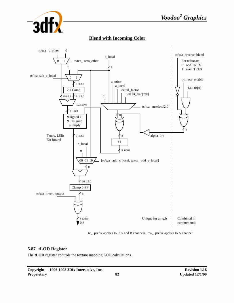
Voodoo2 Graphics
Copyright 1996-1998 3Dfx Interactive, Inc. Revision 1.16 Proprietary 82 Updated 12/1/99
Blend with Incoming Color
8
9 1.8.0
9 1.8.08 0.8.0
8 Color
10 1.9.0
Clamp 0-FF
8
0.8
tc/tca_invert_output
9 signed x 9 unsigned
multiply
Trunc. LSBsNo Round
9 1.8.0
2’s Comp
tc/tca_ c_other
tc/tca_sub_c_local
8 0.8.0
0
0 1
c_local
8
9 0.9.0
+1
8
tc/tca_ mselect[2:0]
LODB[0]
0
a_locala_other
detail_factorLODB_frac[7:0]
trilinear_enable
tc/tca_reverse_blend
{tc/tca_ add_c_local, tc/tca_ add_a_local}
8
0
00 10
Combined in common unit
Unique for a,r,g,b
1
For trilinear:0: odd TREX1: even TREX
tc/tca_ zero_other
0
0 1
alpha_inv
a_local
01
tc_ prefix applies to R,G and B channels. tca_ prefix applies to A channel.
[0,0x100]
5.87 tLOD Register The tLOD register controls the texture mapping LOD calculations.

Voodoo2 Graphics
Copyright 1996-1998 3Dfx Interactive, Inc. Revision 1.16 Proprietary 83 Updated 12/1/99
Bit Name Description 5:0 lodmin Minimum LOD. (4.2 unsigned) 11:6 lodmax Maximum LOD. (4.2 unsigned) 17:12 lodbias LOD Bias. (4.2 signed) 18 lod_odd LOD odd (0=even, 1=odd) 19 lod_tsplit Texture is Split. (0=texture contains all LOD levels, 1=odd or even levels only, as
controlled by lod_odd) 20 lod_s_is_wider S dimension is wider, for rectilinear texture maps. This is a don’t care for square
textures. (1=S is wider than T). 22:21 lod_aspect Aspect ratio. Equal to 2^n. (00 is square texture, others are rectilinear: 01 is
2x1/1x2, 10 is 4x1/1x4, 10 is 8x1/1x8) 23 lod_zerofrac LOD zero frac, useful for bilinear when even and odd levels are split across two
Bruces (0=normal LOD frac, 1=force fraction to 0) 24 tmultibaseaddr Use multiple texbaseAddr registers 25 tdata_swizzle Byte swap incoming texture data (bytes 0<->3, 1<->2). 26 tdata_swap Short swap incoming texture data (shorts 0<->1). 27 tdirect_write Enable raw direct texture memory writes (1=enable). seq_8_downld must equal 0. lodbias is added to the calculated LOD value, then it is clamped to the range [lodmin, min(8.0, lodmax)]. Note that whether the LOD is clamped to lodmin is used to determine whether to use the minification or magnification filter, selected by the tminfilter and tmagfilter bits of textureMode:
LOD bias, clamp
0256x256
81x1
LOD
LODmaxLODmin
tmagfiltertminfilter
The tdata_swizzle and tdata_swap bits in tLOD are used to modify incoming texture data for endian dependencies. The tdata_swizzle bit causes incoming texture data bytes to be byte order reversed, such that bits(31:24) are swapped with bits(7:0), and bits(23:16) are swapped with bits(15:8). Short-word swapping is performed after byte order swizzling, and is selected by the tdata_swap bit in tLOD. When enabled, short-word swapping causes the post-swizzled 16-bit shorts to be order reversed, such that bits(31:16) are swapped with bits(15:0). The following diagram shows the data manipulation functions perfomed by the tdata_swizzle and tdata_swap bits:

Voodoo2 Graphics
Copyright 1996-1998 3Dfx Interactive, Inc. Revision 1.16 Proprietary 84 Updated 12/1/99
3
Incoming Texture Data
2 1 0 (Bytes 0-3)
1 01 00 10 1 tdata_swizzle
1 0 (Shorts 0-1)
0 1 1 0 tdata_swap
32
8888
8888
16
1616
16
Texture MemoryData [15:0]
Texture MemoryData [31:16]
5.88 tDetail Register The tDetail register controls the detail texture. Bit Name Description 7:0 detail _max Detail texture LOD clamp (8.0 unsigned) 13:8 detail_bias Detail texture bias (6.0 signed) 16:14 detail_scale Detail texture scale shift left 17 rgb_tminfilter RGB texture minification filter (0=point-sampled, 1=bilinear) 18 rgb_tmagfilter RGB texture magnification filter (0=point-sampled, 1=bilinear) 19 a_tminfilter Alpha texture minification filter (0=point-sampled, 1=bilinear) 20 a_tmagfilter Alpha texture magnification filter (0=point-sampled, 1=bilinear) 21 rgb_a_separate_filter 0=tminfilter and tmagfilter (in textureMode) define the filter for
RGBA 1=rgb_tminfilter/rgb_tmagfilter define the filter for RGB and a_tminfilter/a_tmagfilter define the filter for Alpha
detail_factor is used in the Texture Combine Unit to blend between the main texture and the detail texture. detail_factor (0.8 unsigned) = max(detail_max, ((detail_bias - LOD) << detail_scale))

Voodoo2 Graphics
Copyright 1996-1998 3Dfx Interactive, Inc. Revision 1.16 Proprietary 85 Updated 12/1/99
When rgb_a_separate_filter is set, rgb_tminfilter and rgb_tmagfilter are used for RGB filtering and a_tminfilter and a_tmagfilter are used for Alpha filtering. When rgb_a_separate_filter is cleared, tminfilter and tmagfilter (in textureMode) are used for RGBA filtering.
5.89 texBaseAddr, texBaseAddr1, texBaseAddr2, and texBaseAddr38 Registers The texBaseAddr register specifies the starting texture memory address for accessing a texture, at a granularity of 8 bytes. It is used for both texture writes and rendering. Calculation of the texbaseaddr is described in the Texture Memory Access section 10. Selection of the base address is a function of tmultibaseaddr and LODBI. Bit Name Description 18:0 texbaseaddr Texture Memory Base Address, tmultibaseaddr==0 or LODBI==0 18:0 texbaseaddr1 Texture Memory Base Address, tmultibaseaddr==1 and LODBI==1 18:0 texbaseaddr2 Texture Memory Base Address, tmultibaseaddr==1 and LODBI==2 18:0 texbaseaddr38 Texture Memory Base Address, tmultibaseaddr==1 and LODBI>=3 .
5.90 trexInit0 Register The trexInit0 register is used for hardware initialization and configuration of the Bruce chip(s). FIXME. See Bruce spec.
5.91 trexInit1 Register The trexInit1 register is used for hardware initialization and configuration of the Bruce chip(s). FIXME. See Bruce spec.
5.92 nccTable0 and nccTable1/Palette Registers The nccTable0 and nccTable1 registers contain two Narrow Channel Compression (NCC) tables used to store lookup values for compressed textures (used in YIQ and AYIQ texture formats as specified in tformat of textureMode). These registers are also used to write the palette.
5.92.1 NCC Table Two tables are stored so that they can be swapped on a per-triangle basis when performing multi-pass rendering, thus avoiding a new download of the table. Use of either nccTable0 or nccTable1 is selected by the Narrow Channel Compressed (NCC) Table Select bit of textureMode. nccTable0 and nccTable1 are stored in the format of the table below, and are write only. nccTable Address Bits Contents
0 31:0 {Y3[7:0], Y2[7:0], Y1[7:0], Y0[7:0]} 1 31:0 {Y7[7:0], Y6[7:0], Y5[7:0], Y4[7:0]} 2 31:0 {Yb[7:0], Ya[7:0], Y9[7:0], Y8[7:0]} 3 31:0 {Yf[7:0], Ye[7:0], Yd[7:0], Yc[7:0]} 4 26:0 {I0_r[8:0], I0_g[8:0], I0_b[8:0]} 5 26:0 {I1_r[8:0], I1_g[8:0], I1_b[8:0]} 6 26:0 {I2_r[8:0], I2_g[8:0], I2_b[8:0]} 7 26:0 {I3_r[8:0], I3_g[8:0], I3_b[8:0]} 8 26:0 {Q0_r[8:0], Q0_g[8:0], Q0_b[8:0]} 9 26:0 {Q1_r[8:0], Q1_g[8:0], Q1_b[8:0]} 10 26:0 {Q2_r[8:0], Q2_g[8:0], Q2_b[8:0]}
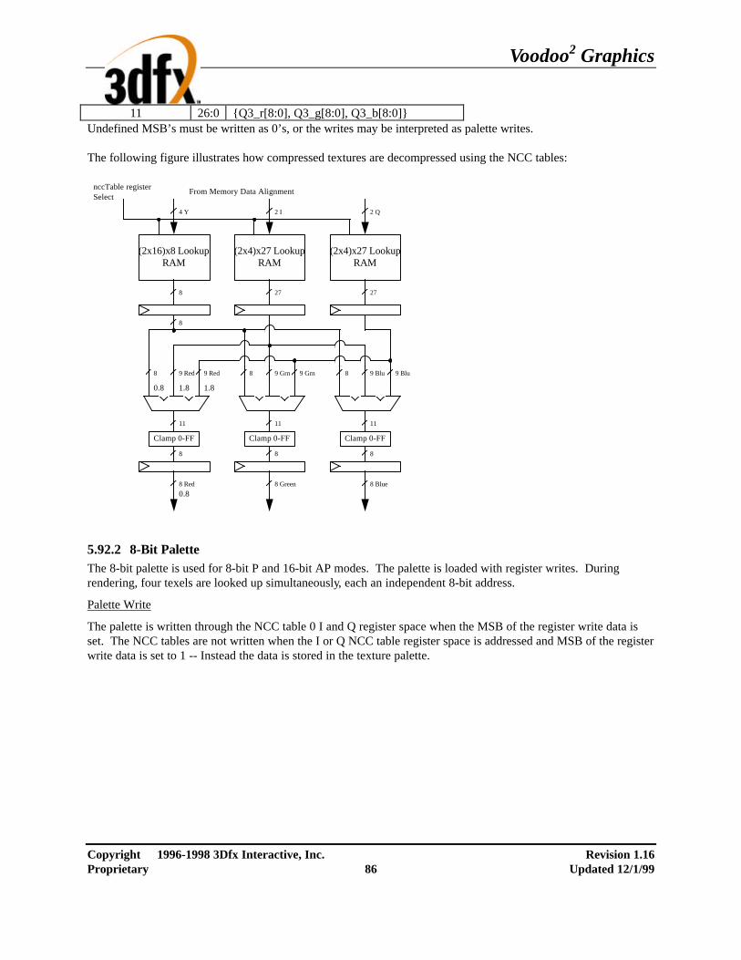
Voodoo2 Graphics
Copyright 1996-1998 3Dfx Interactive, Inc. Revision 1.16 Proprietary 86 Updated 12/1/99
11 26:0 {Q3_r[8:0], Q3_g[8:0], Q3_b[8:0]} Undefined MSB’s must be written as 0’s, or the writes may be interpreted as palette writes. The following figure illustrates how compressed textures are decompressed using the NCC tables:
(2x16)x8 LookupRAM
4 Y
8
(2x4)x27 LookupRAM
2 I
27
(2x4)x27 LookupRAM
2 Q
27
8
8 9 Red 9 Red 8 9 Grn 9 Grn 8 9 Blu 9 Blu
8 Red 8 Green 8 Blue
11
Clamp 0-FF
8
11
Clamp 0-FF
8
11
Clamp 0-FF
8
0.8 1.8 1.8
0.8
nccTable registerSelect
From Memory Data Alignment
5.92.2 8-Bit Palette The 8-bit palette is used for 8-bit P and 16-bit AP modes. The palette is loaded with register writes. During rendering, four texels are looked up simultaneously, each an independent 8-bit address.
Palette Write
The palette is written through the NCC table 0 I and Q register space when the MSB of the register write data is set. The NCC tables are not written when the I or Q NCC table register space is addressed and MSB of the register write data is set to 1 -- Instead the data is stored in the texture palette.
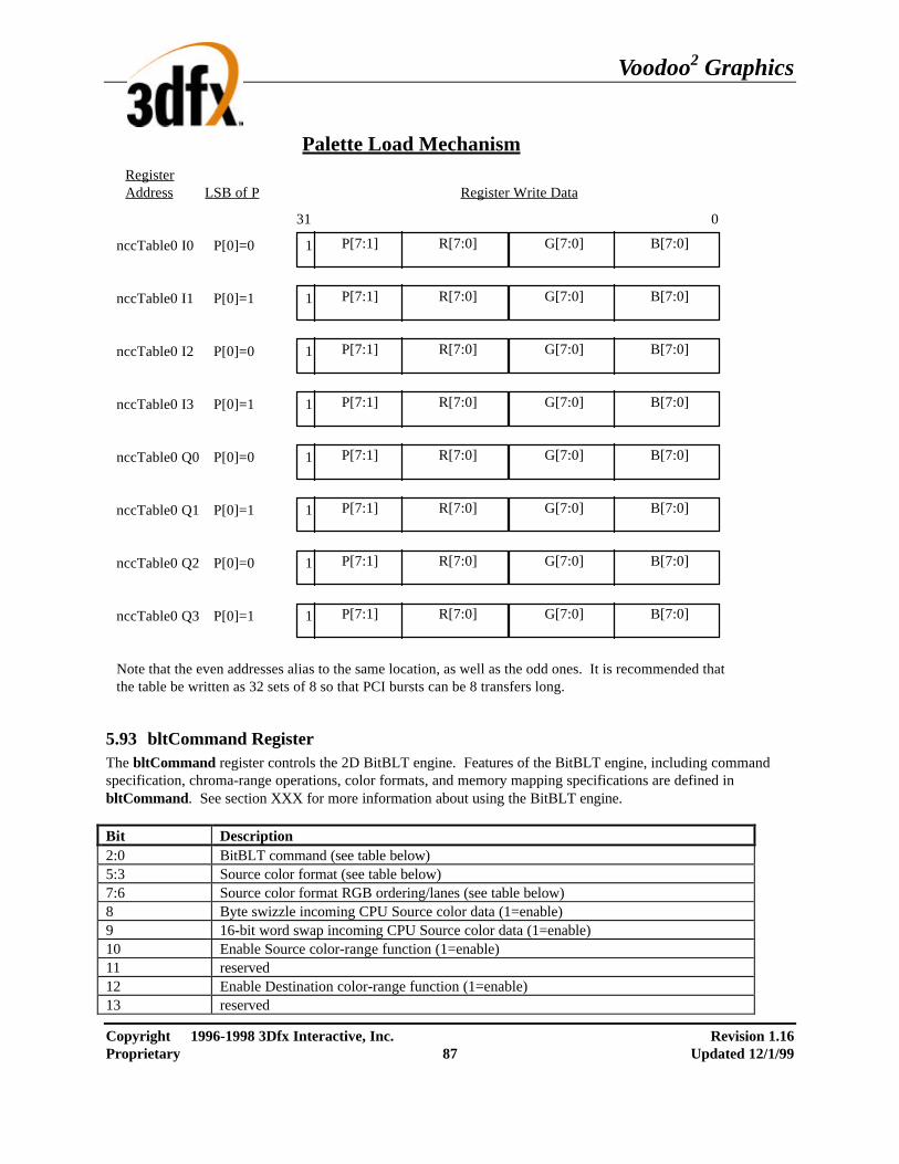
Voodoo2 Graphics
Copyright 1996-1998 3Dfx Interactive, Inc. Revision 1.16 Proprietary 87 Updated 12/1/99
Palette Load Mechanism
nccTable0 I0
31 0
G[7:0] B[7:0]1 R[7:0]P[7:1]P[0]=0
Register Write DataRegisterAddress LSB of P
nccTable0 I1 G[7:0] B[7:0]1 R[7:0]P[7:1]P[0]=1
nccTable0 I2 G[7:0] B[7:0]1 R[7:0]P[7:1]P[0]=0
nccTable0 I3 G[7:0] B[7:0]1 R[7:0]P[7:1]P[0]=1
nccTable0 Q0 G[7:0] B[7:0]1 R[7:0]P[7:1]P[0]=0
nccTable0 Q1 G[7:0] B[7:0]1 R[7:0]P[7:1]P[0]=1
nccTable0 Q2 G[7:0] B[7:0]1 R[7:0]P[7:1]P[0]=0
nccTable0 Q3 G[7:0] B[7:0]1 R[7:0]P[7:1]P[0]=1
Note that the even addresses alias to the same location, as well as the odd ones. It is recommended that the table be written as 32 sets of 8 so that PCI bursts can be 8 transfers long.
5.93 bltCommand Register The bltCommand register controls the 2D BitBLT engine. Features of the BitBLT engine, including command specification, chroma-range operations, color formats, and memory mapping specifications are defined in bltCommand. See section XXX for more information about using the BitBLT engine. Bit Description 2:0 BitBLT command (see table below) 5:3 Source color format (see table below) 7:6 Source color format RGB ordering/lanes (see table below) 8 Byte swizzle incoming CPU Source color data (1=enable) 9 16-bit word swap incoming CPU Source color data (1=enable) 10 Enable Source color-range function (1=enable) 11 reserved 12 Enable Destination color-range function (1=enable) 13 reserved

Voodoo2 Graphics
Copyright 1996-1998 3Dfx Interactive, Inc. Revision 1.16 Proprietary 88 Updated 12/1/99
14 Memory mapping for Source is tiled (0=linear, 1=32x32 tiles) 15 Memory mapping for Destination is tiled (0=linear, 1=32x32 tiles) 16 Enable 2D BitBLT clipping rectangle (1=enable) 17 Transparent monochrome (1=transparent) 30:18 reserved 31 Begin BitBLT operation execution Bits(2:0) of bltCommand specify the BitBLT command to be executed. The table below shows the supported BitBLT commands:
bltCommand(2:0) Command 0 Screen-to-Screen BitBLT 1 CPU-to-screen BitBLT 2 BitBLT Rectangle Fill 3 SGRAM fill (uses SGRAM-specific color expansion) 7-4 Reserved A Screen-to-Screen BitBLT command is used to transfer data from frame buffer memory to frame buffer memory. The Source and Destination regions for Screen-to-Screen BitBLTs may be on-screen or off-screen, and different memory mappings and configurations (ie. strides, tiled memory, linear memory, etc.) are independently selectable for each region. Both the Source and Destination color format must be 16 bits-per-pixel for all Screen-to-Screen BLT operations. Data is stored into the Destination memory region at a maximum rate of one pixel per 2 clocks. A CPU-to-Screen BitBLT command is used to transfer data from the Host/System memory to frame buffer memory. For CPU-to-Screen BitBLTs, data is passed by the CPU through the bltData register, and, as a function of the Source color format, converted into the 16 bits-per-pixel Destination frame buffer. The memory mapping and configuration of the Destination memory region is programmable. Data is stored into the Destination memory region at a maximum rate of one pixel per clock. A BitBLT Rectangle Fill command is used to fill the Destination frame buffer memory with a constant value. The memory mapping and configuration of the Destination memory region is programmable. Using the BitBLT Rectangle Fill, the data value specified by bltColor bits(15:0) is stored into the Destination memory region at a maximum rate of one pixel per clock. When using the SGRAM fill command (which uses the SGRAM color expansion capability, selectable by bltCommand bits(2:0)=3), only entire pages may be filled with a constant value (i.e. block regions smaller than an entire SGRAM page cannot be cleared using the SGRAM fill command). SGRAM fills also bypass any selected clipping or chroma-range tests, and do not use ROPs – data is always written into the frame buffer. Setting up a SGRAM fill command consists of setting the starting row address (or page number) of the SGRAM page in bltDstXY bits(24:16), the starting column address (or page offset) in bltDstXY bits(8:0), the number of complete pages to fill in bltSize(24:16), and the number of columns to fill in bltSize(8:0). When using the SGRAM fill command, the data value specified by bltColor bits(15:0) is stored into the Destination memory region at a maximum rate of 16 pixels per clock. The BitBLT engine only supports 16BPP (5-6-5 RGB) Destination color format. Bits(5:3) of bltCommand specify the format of the Source data for Screen-to-Screen and CPU-to-Screen BLTs. The table below shows the Source color formats supported:
bltCommand(5:3) Source Color Format 0 1 BPP (monochrome, “standard” format) 1 1 BPP (monochrome, “byte-packed” format)

Voodoo2 Graphics
Copyright 1996-1998 3Dfx Interactive, Inc. Revision 1.16 Proprietary 89 Updated 12/1/99
2 16 BPP (5-6-5 RGB) 3 24 BPP (8-8-8 RGB, undithered) 4 24 BPP (8-8-8 RGB, 2x2 ordered dithered) 5 24 BPP (8-8-8 RGB, 4x4 ordered dithered) 7-6 Reserved For Screen-to-Screen BLTs, only 16BPP Source color format is supported, and so the values of bltCommand bits(5:3) are ignored for Screen-to-Screen BLTs. BltCommand bits(5:3) are also ignored for Rectangle Fills. For CPU-to-Screen BLTs, all color formats specified in the table above are supported. For monochrome data formats, a single 32-bit CPU Source word can generate up to 32 16 BPP Destination pixels generated by the BitBLT engine. For the 16-bit Source color format, a single 32-bit Source word can generate up to 2 pixels generated by the BitBLT engine. There are three 24-bit Source color formats: 2x2 dithered, 4x4 dithered and undithered. For the undithered 24-bit Source color format, data must be transferred from the CPU as unpacked, 32-bit words for each 24-bit Source pixel to be displayed. The 24-bit data is then converted into the 16 BPP Destination pixel format by bit truncation. For the dithered 24-bit Source color format, data is transferred from the CPU as packed, 32-bit words for each 24-bit Source pixel, and the 24 BPP Source pixel is converted into the 16 BPP Destination pixel format using either a 2x2 or 4x4 ordered dithering algorithm. Bits(7:6) of bltCommand specify the RGB channel format (or “color lanes”) for the CPU Source data for CPU-to-Screen BLTs. The table below shows the supported RGB lanes for CPU Source BLT data: bltCommand(7:6) RGB Channel Format 0 ARGB 1 ABGR 2 RGBA 3 BGRA The values of bltCommand bits(7:6) are ignored for Screen-to-Screen BLTs and Rectangle Fills. The following table illustrates the relationship between the color ordering of the Source data and the desired color format:
bltCommand(7:6) (RGB Color Format)
bltCommand(5:3) Source Color Format
RGB Channels within Source BLT Data
0 (ARGB) 2 (16-bit, 5-6-5) Red (15:11), Green(10:5), Blue(4:0) 1 (ABGR) 2 (16-bit, 5-6-5) Blue (15:11), Green(10:5), Red(4:0) 2 (RGBA) 2 (16-bit, 5-6-5) Red (15:11), Green(10:5), Blue(4:0) 3 (BGRA) 2 (16-bit, 5-6-5) Blue (15:11), Green(10:5), Red(4:0) 0 (ARGB) 3,4,5 (24-bit, 8-8-8) Ignored(31:24), Red (23:16), Green(15:8), Blue(7:0) 1 (ABGR) 3,4,5 (24-bit, 8-8-8) Ignored(31:24), Blue(23:16), Green(15:8), Red(7:0) 2 (RGBA) 3,4,5 (24-bit, 8-8-8) Red(31:24), Green(23:16), Blue(15:8), Ignored(7:0) 3 (BGRA) 3,4,5 (24-bit, 8-8-8) Blue(31:24), Green(23:16), Red(15:8), Ignored(7:0) The RGB color format field in bltCommand (bits(7:6) has no affect on functionality when the CPU Source color format is monochrome data (bltCommand(5:3)=0 or bltCommand(5:3)=1). Bit(8) of bltCommand enables byte swizzling of the CPU Source BLT data for CPU-to-Screen BLTs. When bit(8)=1, then the byte formed by bits(31:24) is exchanged with the byte formed by bits(7:0) of the 32-bit Source BLT data, and the byte formed by bits(23:16) is exchanged with the byte formed by bits(15:8). Bit 9 of bltCommand enables 16-bit word swapping. When bit(9)=1, then the 16-bit word formed by bits(31:16) of the 32-
Voodoo2 Graphics
Copyright 1996-1998 3Dfx Interactive, Inc. Revision 1.16 Proprietary 90 Updated 12/1/99
bit Source BLT data is exchanged with the 16-bit word formed by bits(15:0) of the data. The values of bltCommand bit(8) and bit(9) are ignored for Screen-to-Screen BitBLTs, Rectangle Fills, and SGRAM fills. The order of 16-bit word swapping and byte swizzling operations for CPU-to-Screen BLTs is as follows: byte swizzling is performed first on all incoming CPU Source BLT data, as defined by bltCommand bit(8) and regardless of the Source BLT color format (bltCommand(5:3)). After byte swizzling, 16-bit word swapping is performed as defined by bltCommand bit(9) and regardless of the Source BLT color format. Note that 16-bit word swapping is performed on the Source BLT data that was previously optionally byte swizzled. Finally, after both byte swizzling and 16-bit word swapping are performed, the individual color channels are selected as defined in bltCommand bits(7:6). Note that the color channels are selected on the Source BLT data that was previously byte swizzled and/or 16-bit word swapped. Bit(12) and bit(10) of bltCommand control the BLT chroma-ranging tests. Bit(10) enables the Source pixel chroma-range test, and bit(12) enables the Destination pixel chroma-range test. When the Source chroma-range test is disabled (bltCommand bit(10)=0), the result of the Source chroma-range test is forced to “fail.” Similarly, when the Destination chroma-range test is disabled (bltCommand bit(12)=0), the result of the Destination chroma-range test is forced to “fail.” The comparison results from both the Source chroma-range and Destination chroma-range tests are used to select the ROP for a given pixel. See the bltSrcChromaRange, bltDstChromaRange, and bltRop register descriptions for more information. Bits(15:14) of bltCommand control the memory mapping type of the Source and Destination BLT areas. When bit(14)=1, the Source BLT memory area is defined to be mapped using the 32x32 tiling algorithm, and when bit(14)=0 the Source BLT memory area is defined to be linearly memory mapped. Similarly, when bit(15)=1, the Destination BLT memory area is defined to be mapped using the 32x32 tiling algorithm, and bit(15)=0 defines the Destination BLT memory area to be linearly mapped. Note that the setting of bltCommand bits(15:14) have no effect on SGRAM fill commands. See the bltSrcBaseAddr, bltDstBaseAddr, and bltXYStrides register descriptions for more information on memory mapping. Bit(16) of bltCommand is used to enable the 2D BitBLT clipping register. When bit(16)=1, all 2D BitBLT Destination XY values are clipped to the rectangle defined by the bltClipX and bltClipY registers. When BitBLT clipping is enabled (bltCommand bit(16)=1), if the XY Destination coordinates lie outside the clipping rectangle defined by bltClipX and bltClipY, the pixel is invalided in the BitBLT drawing pipeline and the pixel is not written to the frame buffer. Note that when clipping is enabled, the bounding clipping rectangle must always be less than or equal to the screen resolution in order to clip to screen coordinates. Also note that if BitBLT clipping is disabled, 2D BitBLT drawing must be programmed to guarantee drawing is never outside the screen resolution. All 2D drawing commands are subject to clipping when bltCommand bit(16)=1 with the exception of SGRAM fill command, which ignores the state of bltCommand bit(16). Bit(17) of bltCommand is used to control whether monochrome Source data is transparent or opaque. When bit(17)=0, monochrome Source data is opaque; the value ‘0’ within the monochrome Source data is expanded into the 16-bit Background color, specified by BltColor bits(31:0). When bltCommand bit(17)=1, monochrome Source data is transparent; the value ‘0’ within the monochrome Source data results in the corresponding Destination pixel to be unchanged. Note that bltCommand bit(17) has no effect on Screen-to-Screen BLTs, rectangle fills, and SGRAM fills. Bit(31) of bltCommand is used to launch the BitBLT operation. BitBLT operations may be launched by writing the value ‘1’ to bit(31) of bltCommand, bit(31) of bltDstXY, or bit(31) of bltSize. Launching a BitBLT operation causes the BLT to begin execution. For Screen-to-Screen BLTs and Rectangle Fills, launching a BitBLT operation causes the entire block region defined by the bltSrcXY, bltDstXY, and bltSize registers to be filled. For CPU-to-Screen BitBLTs, launching a BitBLT operation causes the BitBLT engine to wait for CPU Source data to be sent

Voodoo2 Graphics
Copyright 1996-1998 3Dfx Interactive, Inc. Revision 1.16 Proprietary 91 Updated 12/1/99
through the bltData register – each 32-bit Source data word sent by the CPU results in between 1 and 32 pixels (depending on the CPU Source color format) to be generated in the Destination block region. Note that all registers which are used by a particular BitBLT operation must be properly setup before launching the BitBLT operation.
5.94 bltSrcBaseAddr The bltSrcBaseAddr register specifies the base address for the Source BLT data for Screen-to-Screen BLTs. The value stored in bltSrcBaseAddr is a function of whether the Source BLT data area is linearly mapped or tiled. When the Source BLT data area is linearly mapped (bltCommand bit(14)=0), bltSrcBaseAddr specifies the base linear frame buffer address for address calculations. The base address for Source BLT data must be aligned on an 8-byte boundry, and so the low 3-bits of bltSrcBaseAddr must be stored with the value 000. See the bltXYStrides register description for more information on memory mapping and how XY coordinates are converted into linear frame buffer addresses. bltSrcBaseAddr, with linearly mapped Source BLT data (bltCommand(14)=0) Bit Description 2:0 Value ignored for address calculations. Software must store the value 000. 21:3 Base address for Screen-to-Screen Source BLT data [range 0-4 MBytes] When the Source BLT data area is tiled (bltCommand bit(14)=1), bltSrcBaseAddr specifies the base page address (or row value) for address calculations. See the bltXYStrides register description for more information on memory mapping and how XY coordinates are converted into linear frame buffer addresses. bltSrcBaseAddr, with 32x32 tiled Source BLT data (bltCommand(14)=1) Bit Description 9:0 Base row for Screen-to-Screen Source BLT data [range 0-1023]
5.95 bltDstBaseAddr The bltDstBaseAddr register specifies the base address for the Destination BLT data for Screen-to-Screen BitBLTs, CPU-to-Screen BitBLTs, and BitBLT Rectangle Fills (SGRAM fills does not use the bltDstBaseAddr). When the Destination BLT data area is linearly mapped (bltCommand bit(15)=0), bltDstBaseAddr specifies the base linear frame buffer address for address calculations. The base address for Destination BLT data must be aligned on an 8-byte boundry, and so the low 3-bits of bltDstBaseAddr must be stored with the value 000. See the bltXYStrides register description for more information on memory mapping and how XY coordinates are converted into linear frame buffer addresses. bltDstBaseAddr, with linearly mapped Destination BLT data (bltCommand(15)=0) Bit Description 2:0 Value ignored for address calculations. Software must store the value 000. 21:3 Base address for Screen-to-Screen Destination BLT data [range 0-4 Mbytes] When the Destination BLT data area is tiled (bltCommand bit(15)=1), bltDstBaseAddr specifies the base page address (or row value) for address calculations. See the bltXYStrides register description for more information on memory mapping and how XY coordinates are converted into linear frame buffer addresses.
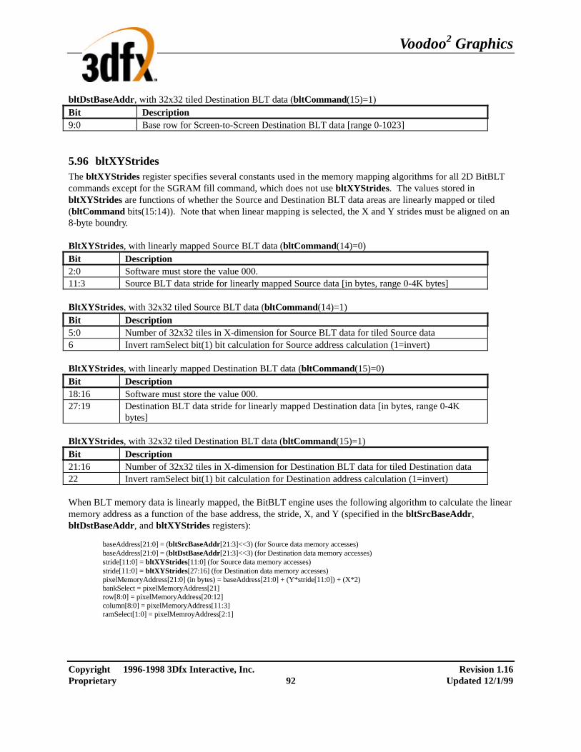
Voodoo2 Graphics
Copyright 1996-1998 3Dfx Interactive, Inc. Revision 1.16 Proprietary 92 Updated 12/1/99
bltDstBaseAddr, with 32x32 tiled Destination BLT data (bltCommand(15)=1) Bit Description 9:0 Base row for Screen-to-Screen Destination BLT data [range 0-1023]
5.96 bltXYStrides The bltXYStrides register specifies several constants used in the memory mapping algorithms for all 2D BitBLT commands except for the SGRAM fill command, which does not use bltXYStrides. The values stored in bltXYStrides are functions of whether the Source and Destination BLT data areas are linearly mapped or tiled (bltCommand bits(15:14)). Note that when linear mapping is selected, the X and Y strides must be aligned on an 8-byte boundry. BltXYStrides, with linearly mapped Source BLT data (bltCommand(14)=0) Bit Description 2:0 Software must store the value 000. 11:3 Source BLT data stride for linearly mapped Source data [in bytes, range 0-4K bytes] BltXYStrides, with 32x32 tiled Source BLT data (bltCommand(14)=1) Bit Description 5:0 Number of 32x32 tiles in X-dimension for Source BLT data for tiled Source data 6 Invert ramSelect bit(1) bit calculation for Source address calculation (1=invert) BltXYStrides, with linearly mapped Destination BLT data (bltCommand(15)=0) Bit Description 18:16 Software must store the value 000. 27:19 Destination BLT data stride for linearly mapped Destination data [in bytes, range 0-4K
bytes] BltXYStrides, with 32x32 tiled Destination BLT data (bltCommand(15)=1) Bit Description 21:16 Number of 32x32 tiles in X-dimension for Destination BLT data for tiled Destination data 22 Invert ramSelect bit(1) bit calculation for Destination address calculation (1=invert) When BLT memory data is linearly mapped, the BitBLT engine uses the following algorithm to calculate the linear memory address as a function of the base address, the stride, X, and Y (specified in the bltSrcBaseAddr, bltDstBaseAddr, and bltXYStrides registers):
baseAddress[21:0] = (bltSrcBaseAddr[21:3]<<3) (for Source data memory accesses) baseAddress[21:0] = (bltDstBaseAddr[21:3]<<3) (for Destination data memory accesses) stride[11:0] = bltXYStrides[11:0] (for Source data memory accesses) stride[11:0] = bltXYStrides[27:16] (for Destination data memory accesses) pixelMemoryAddress[21:0] (in bytes) = baseAddress[21:0] + (Y*stride[11:0]) + (X*2) bankSelect = pixelMemoryAddress[21] row[8:0] = pixelMemoryAddress[20:12] column[8:0] = pixelMemoryAddress[11:3] ramSelect[1:0] = pixelMemroyAddress[2:1]

Voodoo2 Graphics
Copyright 1996-1998 3Dfx Interactive, Inc. Revision 1.16 Proprietary 93 Updated 12/1/99
When BLT memory data is tiled, the BitBLT engine uses the following algorithm to calculate the linear memory address as a function of the base address, the number of 32x32 tiles in the X dimension, X, and Y (specified in the bltSrcBaseAddr, bltDstBaseAddr, and bltXYStrides registers):
tilesInX[4:0] = bltXYStrides[4:0] (for Source data memory accesses) tilesInX[4:0] = bltXYStrides[20:16] (for Destination data memory accesses) rowBase[9:0] = bltSrcBaseAddr[9:0] (for Source data memory accesses) rowBase[9:0] = bltDstBaseAddr[9:0] (for Destination data memory accesses) invertRamSelect = bltXYStrides[5] (for Source data memory accesses) invertRamSelect = bltXYStrides[21] (for Destination data memory accesses) rowStart[9:0] = ((Y>>5) * tilesInX) >> 1 rowOffset[9:0] = (!(Y&0x20) || !(tilesInX & 0x1)) ? (X>>6) : ((X>31) ? (((X-32)>>6)+1) : 0) row[9:0] = rowBase + rowStart + rowOffset (software must guarantee now overflows…) column[8:0] = ((Y % 32) <<4) + ((X % 32)>>1)
ramSelect[1] =(!(tilesInX&0x1)) ? ((X&0x20) ? 1 : 0) : (((X&0x20)^(Y&0x20)) ? 1 : 0) ^ invertRamSelect ramSelect[0] = X % 2 pixelMemoryAddress[21:0] = (row[9:0]<<12) + (column[8:0]<<3) + (ramSelect[1:0]<<1) bankSelect = pixelMemoryAddress[21]
As a point of reference, the 3D engine uses the following algorithm to calculate the linear memory address as a function of the video buffer offset (fbiInit2 bits(19:11)), the number of 32x32 tiles in the X dimension (fbiInit1 bits(7:4) and bit(24)), X, and Y:
tilesInX[4:0] = {fbiInit1[24], fbiInit1[7:4], fbiInit6[30]} rowBase = fbiInit2[19:11] rowStart = ((Y>>5) * tilesInX) >> 1 rowOffset = (!(Y&0x20) || !(tilesInX & 0x1)) ? (X>>6) : ((X>31) ? (((X-32)>>6)+1) : 0) row[9:0] = rowStart + rowOffset (for color buffer 0) row[9:0] = rowBase + rowStart + rowOffset (for color buffer 1) row[9:0] = (rowBase<<1) + rowStart + rowOffset (for depth/alpha buffer when double color buffering[fbiInit5[10:9]=0]) row[9:0] = (rowBase<<1) + rowStart + rowOffset (for color buffer 2 when triple color buffering[fbiInit5[10:9]=1 or 2]) row[9:0] = (rowBase<<1) + rowBase + rowStart + rowOffset (for depth/alpha buffer when triple color buffering[fbiInit5[10:9]=2]) column[8:0] = ((Y % 32) <<4) + ((X % 32)>>1)
ramSelect[1] =(!(tilesInX&0x1)) ? ((X&0x20) ? 1 : 0) : (((X&0x20)^(Y&0x20)) ? 1 : 0) (for color buffers) ramSelect[1] =(!(tilesInX&0x1)) ? ((X&0x20) ? 0 : 1) : (((X&0x20)^(Y&0x20)) ? 0 : 1) (for depth/alpha buffers) ramSelect[0] = X % 2 pixelMemoryAddress[21:0] = (row[9:0]<<12) + (column[8:0]<<3) + (ramSelect[1:0]<<1) bankSelect = pixelMemoryAddress[21]
5.97 bltSrcChromaRange The bltSrcChromaRange register specifies minimum and maximum 16-bit RGB color values which are compared to the 2D BitBLT Source pixels when the Source chroma-range comparison function is enabled (bltCommand bit(10)=1). The comparison results of the Source and Destination chroma-range tests are used to select one of four possible ROPs (defined in the bltRop register). A 2D BitBLT Source pixel color may be compared to the color range formed by the minimum and maximum colors stored in the bltSrcChromaRange register. Software must program the minimum color value to be less than or equal to the value of the maximum color. The Source chroma-range test “Passes” if the Source pixel color is within the range (greater than or equal to the minimum color and less than or equal to the maximum color) of the colors specified in bltSrcChromaRange and the Source chroma-range test is enabled (bltCommand bit(10)=1). The Source chroma-range test “Fails” if the Source pixel color is less than the minimum color or greater than the maximum color. A “Fail” condition for the Source chroma-range test may be forced by disabling the chroma-range test by setting bltCommand bit(10)=0. Note that the SGRAM fill command ignores any chroma-range tests and always writes data directly into frame buffer memory, regardless of the ROPs specified in the bltRop register. See the bltDstChromaRange and bltRop register descriptions for more information. Bit Description

Voodoo2 Graphics
Copyright 1996-1998 3Dfx Interactive, Inc. Revision 1.16 Proprietary 94 Updated 12/1/99
4:0 Source chroma-range test minimum color (5 bits, blue color component) 10:5 Source chroma-range test minimum color (6 bits, green color component) 15:11 Source chroma-range test minimum color (5 bits, red color component) 20:16 Source chroma-range test maximum color (5 bits, blue color component) 26:21 Source chroma-range test maximum color (6 bits, green color component) 31:27 Source chroma-range test maximum color (5 bits, red color component)
5.98 bltDstChromaRange The bltDstChromaRange register specifies minimum and maximum 16-bit RGB color values which are compared to the 2D BitBLT Destination pixels when the Destination chroma-range comparison function is enabled (bltCommand bit(12)=1). The comparison results of the Source and Destination chroma-range tests are used to select one of four possible ROPs (defined in the bltRop register). A 2D BitBLT Destination pixel color may be compared to the color range formed by the minimum and maximum colors stored in the bltDstChromaRange register. Software must program the minimum color value to be less than or equal to the value of the maximum color. The Destination chroma-range test “Passes” if the Destination pixel color is within the range (greater than or equal to the minimum color and less than or equal to the maximum color) of the colors specified in bltDstChromaRange. The Destination chroma-range test “Fails” if the Destination pixel color is less than the minimum color or greater than the maximum color. A “Fail” condition for the Destination chroma-range test may be forced by disabling the chroma-range test by setting bltCommand bit(12)=0.. Note that the SGRAM fill command ignores any chroma-range tests and always writes data directly into frame buffer memory, regardless of the ROPs specified in the bltRop register. See the bltSrcChromaRange and bltRop register descriptions for more information. Bit Description 4:0 Destination chroma-range test minimum color (5 bits, blue color component) 10:5 Destination chroma-range test minimum color (6 bits, green color component) 15:11 Destination chroma-range test minimum color (5 bits, red color component) 20:16 Destination chroma-range test maximum color (5 bits, blue color component) 26:21 Destination chroma-range test maximum color (6 bits, green color component) 31:27 Destination chroma-range test maximum color (5 bits, red color component)
5.99 bltClipX and bltClipY The bltClipX and bltClipY registers specify a rectangle within which all 2D BitBLT drawing operations are confined, except for the SGRAM fill command which bypasses the clip test. If 2D BitBLT pixel to be drawn (specified by the XY coordinates of the Destination pixel) lies outside the 2D BitBLT clip rectangle and 2D BitBLT clipping is enabled (bltCommand(16)=1), then the pixel is not written into the frame buffer. The values in the clipping registers are given in pixel units, and the valid drawing rectangle is inclusive of the bltClipleft and bltClipLowY register values, but exclusive of the bltClipRight and bltClipHighY register values. In other words, if clipping is enabled, a pixel is not written to the frame buffer if the X coordinate of the pixel is less than bltClipLeft or greater than or equal to bltClipRight, or if the Y coordinate of the pixel is less than clipLowY or greater than or equal to bltClipHighY. bltClipLowY must be less than bltClipHighY, and bltClipLeft must be less than bltClipRight. The bltClipX and bltClipY registers are enabled by setting bit(16) in the bltCommand register. When clipping is enabled, the bounding clipping rectangle must always be less than or equal to the screen resolution in order to clip to screen coordinates. Note that if clipping is disabled, 2D BitBLT commands must be programmed such that drawing is guaranteed to occur only inside the boundries of the screen resolution. Also note that the SGRAM fill command ignores any clipping tests and always writes data directly into frame buffer memory.

Voodoo2 Graphics
Copyright 1996-1998 3Dfx Interactive, Inc. Revision 1.16 Proprietary 95 Updated 12/1/99
bltClipX Register Bit Description 11:0 Unsigned integer specifying right clipping rectangle edge (bltClipRight) 15:10 reserved 27:16 Unsigned integer specifying left clipping rectangle edge (bltClipLeft) 31:26 reserved bltClipY Register Bit Description 11:0 Unsigned integer specifying high Y clipping rectangle edge (bltClipHighY) 15:10 reserved 27:16 Unsigned integer specifying low Y clipping rectangle edge (bltClipLowY) 31:26 reserved
5.100 bltSrcXY The bltSrcXY register specifies the starting X and Y coordinates for the Source data for Screen-to-Screen BitBLTs. Screen-to-Screen BitBLTs copy data from the location starting at the coordinates specified in the bltSrcXY register to the location starting at the coordinates specified in the bltDstXY register. The upper left of the screen is (0, 0). Positive X is toward the right and positive Y is toward the bottom of the screen. The XY coordinates are specified as unsigned coordinates, as negative coordinates are not allowed. Software must guarantee that the coordinates specified by the bltSrcXY register access valid data in the frame buffer. Note that the starting XY Source coordinates are independent of the direction of the BitBLT (derived from the sign of the values stored in bltSize). For example, if bltSizeX and bltSizeY are both positive, then the coordinates specified in bltSrcXY point to the upper left corner of the Source BitBLT block region. Conversely, if bltSizeX and bltSizeY are both negative, the coordinates specified in bltSrcXY point to the lower right corner of the Source BitBLT block region. Also note that the value of bltSrcXY is ignored for CPU-to-Screen BitBLTs, Rectangle Fills, and SGRAM fills. Bit Description 10:0 Unsigned integer X coordinate of Screen-to-Screen BLT Source Data (bltSrcXYX)
[range 0 to 2K] 15:11 reserved 26:16 Unsigned integer Y coordinate of Screen-to-Screen BLT Source Data (bltSrcXYY)
[range 0 to 2K]
5.101 bltDstXY The bltDstXY register specifies the starting X and Y coordinates for the Destination data for Screen-to-Screen BitBLTs, CPU-to-Screen BitBLTs, and BitBLT Rectangle Fills. BitBLTs and Rectangle Fills copy data into the location starting at the coordinates specified in the bltDstXY register and fill a block the size of which is specified by the bltSize register. The upper left of the screen is (0, 0). Positive X is toward the right and positive Y is toward the bottom of the screen. The XY coordinates are specified as unsigned coordinates, as negative coordinates are not allowed. Software must guarantee that the coordinates specified by the bltDstXY register access valid data in the frame buffer. Note that the starting XY Destination coordinates are independent of the direction of the BitBLT (derived from the sign of the values stored in bltSize). For example, if bltSizeX and bltSizeY are both positive, then the coordinates specified in bltSrcXY point to the upper left corner of the

Voodoo2 Graphics
Copyright 1996-1998 3Dfx Interactive, Inc. Revision 1.16 Proprietary 96 Updated 12/1/99
Destination BitBLT block region. Conversely, if bltSizeX and bltSizeY are both negative, the coordinates specified in bltSrcXY point to the lower right corner of the Destination BitBLT block region. Bit(31) of bltDstXY is used to launch the BitBLT operation. BitBLT operations may be launched by writing the value ‘1’ to bit(31) of BltCommand, bit(31) of bltDstXY, or bit(31) of bltSize. Launching a BitBLT operation causes the BLT to begin execution. Note that the storing a 32-bit data value to bltDstXY with bit(31)=0 stores the XY coordinates for the BLT Destination data but does not begin BitBLT command execution. However, storing a 32-bit data value to bltDstXY with bit(31)=1 stores the XY coordinates for the BLT Destination data and also commences execution of the BitBLT operation as defined by bltCommand bits(2:0). Screen-to-Screen BLTs, CPU-to-Screen BLTs, and BitBLT Rectangle Fills Bit Description 10:0 Unsigned integer X coordinate of BLT Destination Data (bltDstXYX) [range 0 to 2K] 15:11 reserved 26:16 Unsigned integer Y coordinate of BLT Destination Data (bltDstXYY) [range 0 to 2K] 30:27 reserved 31 Begin BitBLT operation execution The bltDstXY register is also used to specify the starting row and column address of the SGRAM page to fill with the value specified in bltColor bits(15:0) for the SGRAM fill command. When executing the SGRAM fill command, bltDstXY bits(8:0) specify the starting column address of the page to begin filling with constant data and bltDstXY bits(24:16) specify the starting row address (or page number) of the page to begin filling with constant data. For SGRAM fills, bltSize bits(8:0) specify the number of complete columns to fill, and bltSize bits(24:16) specify the number of pages to fill. SGRAM fills Bit Description 8:0 Starting column address to be filled for SGRAM fills 15:9 reserved 24:16 Starting row address to be filled for SGRAM fills
5.102 bltSize The bltSize register specifies the width and height for Screen-to-Screen BitBLTs, CPU-to-Screen BitBLTs, and BitBLT Rectangle Fills. The XY coordinates are specified as signed coordinates in the range -2K to 2K. The number of pixels filled horizontally in the BLT (i.e. the width of the BLT region) is the absolute value of bltSizeX plus one, and the number of partial scanlines stored vertically (i.e. the height of the BLT region) is the absolute value of bltSizeY plus one. A positive value stored in bltSizeX generates a BLT block operation which moves from left-to-right, and a negative value stored in bltSizeX generates a BLT operation which moves from right-to-left. Similarly, a positive value stored in bltSizeY generates a BLT operation which moves from top-to-bottom, and a negative value stored in bltSizeY generates a BLT operation which moves from bottom-to-top. Storing the value 0x0 in bltSizeX generates a single pixel-wide BLT, and storing the value 0x0 in bltSizeY generates a single pixel-high BLT. For CPU-to-Screen BitBLTs, both bltSizeX and bltSizeY must be greater than or equal to zero, as negative sizes are not supported for CPU-to-Screen BLTs. However, negative sizes may be used for rectangle Fills and Screen-to-Screen BLTs. Software must guarantee that the coordinates specified by the bltSize register access valid data in the frame buffer. Bit(31) of bltSize is used to launch the BitBLT operation. BitBLT operations may be launched by writing the value ‘1’ to bit(31) of bltCommand, bit(31) of bltDstXY, or bit(31) of bltSize. Launching a BitBLT operation causes the BLT to begin execution. Note that the storing a 32-bit data value to

Voodoo2 Graphics
Copyright 1996-1998 3Dfx Interactive, Inc. Revision 1.16 Proprietary 97 Updated 12/1/99
bltSize with bit(31)=0 stores the width and height of the BLT block region but does not begin BitBLT command execution. However, storing a 32-bit data value to bltSize with bit(31)=1 stores the width and height of the BLT block region and also commences execution of the BitBLT operation as defined by bltCommand bits(2:0). Screen-to-Screen BLTs, CPU-to-Screen BLTs, and BitBLT Rectangle Fills Bit Description 11:0 Signed integer BitBLT width (bltSizeX) [range -2K to 2K] 15:12 reserved 27:16 Signed integer BitBLT height (bltSizeY) [range -2K to 2K] 30:28 reserved 31 Begin BitBLT operation execution The bltSize register is also used to specify the number of columns and rows to fill with the value specified in bltColor bits(15:0) for the SGRAM fill command. When executing the SGRAM fill command, bltDstXY bits(8:0) specify the starting column address of the page to begin filling with constant data and bltDstXY bits(24:16) specify the starting row address (or page number) of the page to begin filling with constant data. For SGRAM fills, bltSize bits(8:0) specify the number of complete columns to fill, and bltSize bits(24:16) specify the number of pages to fill. SGRAM fills Bit Description 8:0 Number of complete columns to fill for SGRAM fills 15:9 reserved 24:16 Number of rows to fill for SGRAM fills
5.103 bltRop The bltRop register defines the Raster Operations (ROPs) for BitBLT operations. During a BitBLT operation, the value of the 16-bit Source pixel is subject to the Source chroma-range test (as controlled by bltCommand bit (10) and the bltSrcChromaRange register), and the value of the 16-bit Destination pixel is subject to the Destination chroma-range test (as controlled by bltCommand bit(12) and the bltDstChromaRange register). The results of the Source chroma-range test and the Destination chroma-range test cause a ROP to be selected from the bltRop register on a pixel-by-pixel basis as follows:
Source chroma-range Test
Destination chroma-range Test
ROP selected
Fail Fail ROP 0 Fail Pass ROP 1 Pass Fail ROP 2 Pass Pass ROP 3 Bit Description 3:0 ROP 0 raster operation 7:4 ROP 1 raster operation 11:8 ROP 2 raster operation 15:12 ROP 3 raster operation The BitBLT engine supports 16 ROPs, illustrated in the table below:

Voodoo2 Graphics
Copyright 1996-1998 3Dfx Interactive, Inc. Revision 1.16 Proprietary 98 Updated 12/1/99
ROP Value Value stored in Frame Buffer 0x0 0 0x1 ~(Src | Dst) 0x2 ~Src & Dst 0x3 ~Src 0x4 Src & ~Dst 0x5 ~Dst 0x6 Src ^ Dst 0x7 ~(Src & Dst) 0x8 Src & Dst 0x9 ~(Src ^ Dst) 0xA Dst 0xB ~Src | Dst 0xC Src 0xD Src | ~Dst 0xE Src | Dst 0xF 1
The BitBLT engine implements the 16 raster operations by using a 4-to-1 MUX for each bit within an outgoing Destination pixel. The 4-bit data inputs into each 4-to-1 MUX is the ROP value (selected by the Source and Destination chroma-range tests), the MSB of the 2-bit MUX select is the Source pixel bit, and the LSB of the 2-bit MUX select is the Destination pixel bit. Note that the SGRAM fill command ignores all ROPs and always writes data directly into frame buffer memory.
5.104 bltColor The bltColor register specifies constant colors used during BitBLT operations. For CPU-to-Screen BLTs with a monochrome CPU Source color data format (bltCommand(5:3)=0 or bltCommand(5:3)=1), the value ‘1’ within the monochrome Source data is expanded into the 16-bit Foreground color, specified by bltColor bits(15:0). When the monochrome Source data is opaque (specified by bltCommand bit(17)=0), the value ‘0’ within the monochrome Source data is expanded into the 16-bit Background color, specified by bltColor bits(31:16). When the monochrome Source data is transparent (bltCommand bit(17)=1), the value ‘0’ within the monochrome Source data results in the corresponding Destination pixel to be unchanged. For Rectangle Fill BLTs (bltCommand(2:0) = 2) and SGRAM fills (bltCommand(2:0) = 3) the value specified by the Foreground color is used as the color for the solid fill. Bit Description 4:0 Foreground color (5 bits, blue color component) 10:5 Foreground color (6 bits, green color component) 15:11 Foreground color (5 bits, red color component) 20:16 Background color (5 bits, blue color component) 26:21 Background color (6 bits, green color component) 31:27 Background color (5 bits, red color component)
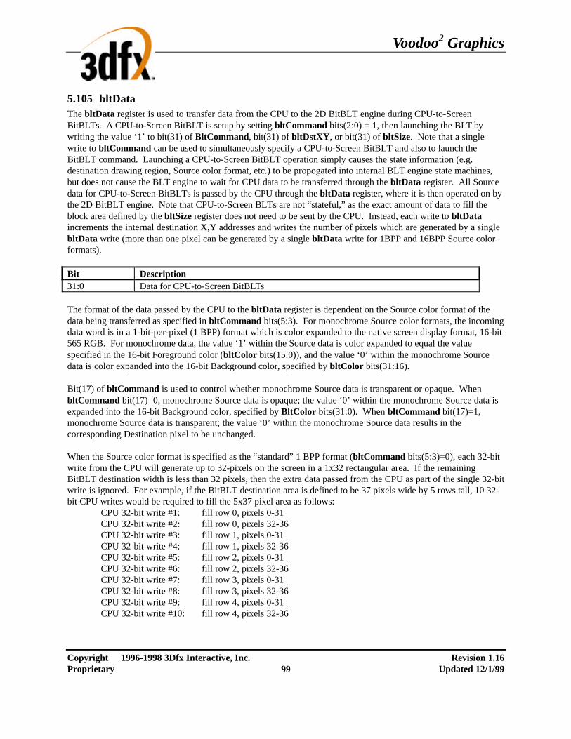
Voodoo2 Graphics
Copyright 1996-1998 3Dfx Interactive, Inc. Revision 1.16 Proprietary 99 Updated 12/1/99
5.105 bltData The bltData register is used to transfer data from the CPU to the 2D BitBLT engine during CPU-to-Screen BitBLTs. A CPU-to-Screen BitBLT is setup by setting bltCommand bits(2:0) = 1, then launching the BLT by writing the value ‘1’ to bit(31) of BltCommand, bit(31) of bltDstXY, or bit(31) of bltSize. Note that a single write to bltCommand can be used to simultaneously specify a CPU-to-Screen BitBLT and also to launch the BitBLT command. Launching a CPU-to-Screen BitBLT operation simply causes the state information (e.g. destination drawing region, Source color format, etc.) to be propogated into internal BLT engine state machines, but does not cause the BLT engine to wait for CPU data to be transferred through the bltData register. All Source data for CPU-to-Screen BitBLTs is passed by the CPU through the bltData register, where it is then operated on by the 2D BitBLT engine. Note that CPU-to-Screen BLTs are not “stateful,” as the exact amount of data to fill the block area defined by the bltSize register does not need to be sent by the CPU. Instead, each write to bltData increments the internal destination X,Y addresses and writes the number of pixels which are generated by a single bltData write (more than one pixel can be generated by a single bltData write for 1BPP and 16BPP Source color formats). Bit Description 31:0 Data for CPU-to-Screen BitBLTs The format of the data passed by the CPU to the bltData register is dependent on the Source color format of the data being transferred as specified in bltCommand bits(5:3). For monochrome Source color formats, the incoming data word is in a 1-bit-per-pixel (1 BPP) format which is color expanded to the native screen display format, 16-bit 565 RGB. For monochrome data, the value ‘1’ within the Source data is color expanded to equal the value specified in the 16-bit Foreground color (bltColor bits(15:0)), and the value ‘0’ within the monochrome Source data is color expanded into the 16-bit Background color, specified by bltColor bits(31:16). Bit(17) of bltCommand is used to control whether monochrome Source data is transparent or opaque. When bltCommand bit(17)=0, monochrome Source data is opaque; the value ‘0’ within the monochrome Source data is expanded into the 16-bit Background color, specified by BltColor bits(31:0). When bltCommand bit(17)=1, monochrome Source data is transparent; the value ‘0’ within the monochrome Source data results in the corresponding Destination pixel to be unchanged. When the Source color format is specified as the “standard” 1 BPP format (bltCommand bits(5:3)=0), each 32-bit write from the CPU will generate up to 32-pixels on the screen in a 1x32 rectangular area. If the remaining BitBLT destination width is less than 32 pixels, then the extra data passed from the CPU as part of the single 32-bit write is ignored. For example, if the BitBLT destination area is defined to be 37 pixels wide by 5 rows tall, 10 32-bit CPU writes would be required to fill the 5x37 pixel area as follows: CPU 32-bit write #1: fill row 0, pixels 0-31 CPU 32-bit write #2: fill row 0, pixels 32-36
CPU 32-bit write #3: fill row 1, pixels 0-31 CPU 32-bit write #4: fill row 1, pixels 32-36
CPU 32-bit write #5: fill row 2, pixels 0-31 CPU 32-bit write #6: fill row 2, pixels 32-36
CPU 32-bit write #7: fill row 3, pixels 0-31 CPU 32-bit write #8: fill row 3, pixels 32-36
CPU 32-bit write #9: fill row 4, pixels 0-31 CPU 32-bit write #10: fill row 4, pixels 32-36
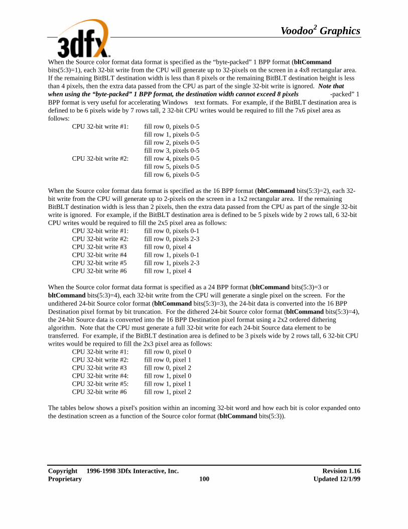
Voodoo2 Graphics
Copyright 1996-1998 3Dfx Interactive, Inc. Revision 1.16 Proprietary 100 Updated 12/1/99
When the Source color format data format is specified as the “byte-packed” 1 BPP format (bltCommand bits(5:3)=1), each 32-bit write from the CPU will generate up to 32-pixels on the screen in a 4x8 rectangular area. If the remaining BitBLT destination width is less than 8 pixels or the remaining BitBLT destination height is less than 4 pixels, then the extra data passed from the CPU as part of the single 32-bit write is ignored. Note that when using the “byte-packed” 1 BPP format, the destination width cannot exceed 8 pixels -packed” 1 BPP format is very useful for accelerating Windows text formats. For example, if the BitBLT destination area is defined to be 6 pixels wide by 7 rows tall, 2 32-bit CPU writes would be required to fill the 7x6 pixel area as follows: CPU 32-bit write #1: fill row 0, pixels 0-5 fill row 1, pixels 0-5 fill row 2, pixels 0-5 fill row 3, pixels 0-5 CPU 32-bit write #2: fill row 4, pixels 0-5 fill row 5, pixels 0-5 fill row 6, pixels 0-5 When the Source color format data format is specified as the 16 BPP format (bltCommand bits(5:3)=2), each 32-bit write from the CPU will generate up to 2-pixels on the screen in a 1x2 rectangular area. If the remaining BitBLT destination width is less than 2 pixels, then the extra data passed from the CPU as part of the single 32-bit write is ignored. For example, if the BitBLT destination area is defined to be 5 pixels wide by 2 rows tall, 6 32-bit CPU writes would be required to fill the 2x5 pixel area as follows: CPU 32-bit write #1: fill row 0, pixels 0-1 CPU 32-bit write #2: fill row 0, pixels 2-3 CPU 32-bit write #3 fill row 0, pixel 4 CPU 32-bit write #4 fill row 1, pixels 0-1 CPU 32-bit write #5 fill row 1, pixels 2-3 CPU 32-bit write #6 fill row 1, pixel 4 When the Source color format data format is specified as a 24 BPP format (bltCommand bits(5:3)=3 or bltCommand bits(5:3)=4), each 32-bit write from the CPU will generate a single pixel on the screen. For the undithered 24-bit Source color format (bltCommand bits(5:3)=3), the 24-bit data is converted into the 16 BPP Destination pixel format by bit truncation. For the dithered 24-bit Source color format (bltCommand bits(5:3)=4), the 24-bit Source data is converted into the 16 BPP Destination pixel format using a 2x2 ordered dithering algorithm. Note that the CPU must generate a full 32-bit write for each 24-bit Source data element to be transferred. For example, if the BitBLT destination area is defined to be 3 pixels wide by 2 rows tall, 6 32-bit CPU writes would be required to fill the 2x3 pixel area as follows: CPU 32-bit write #1: fill row 0, pixel 0 CPU 32-bit write #2: fill row 0, pixel 1 CPU 32-bit write #3 fill row 0, pixel 2 CPU 32-bit write #4: fill row 1, pixel 0 CPU 32-bit write #5: fill row 1, pixel 1 CPU 32-bit write #6 fill row 1, pixel 2 The tables below shows a pixel's position within an incoming 32-bit word and how each bit is color expanded onto the destination screen as a function of the Source color format (bltCommand bits(5:3)).

Voodoo2 Graphics
Copyright 1996-1998 3Dfx Interactive, Inc. Revision 1.16 Proprietary 101 Updated 12/1/99
Bit Position within a 32-bit wordData Format 31 30 29 28 27 26 25 24 23 22 21 20 19 18 17 16 15 14 13 12 11 10 9 8 7 6 5 4 3 2 1 0
1 BPP, standard A24 A25 A26 A27 A28 A29 A30 A31 A16 A17 A18 A19 A20 A21 A22 A23 A8 A9 A10 A11 A12 A13 A14 A15 A0 A1 A2 A3 A4 A5 A6 A71 BPP, byte-packed D0 D1 D2 D3 D4 D5 D6 D7 C0 C1 C2 C3 C4 C5 C6 C7 B0 B1 B2 B3 B4 B5 B6 B7 A0 A1 A2 A3 A4 A5 A6 A7
16BPPA1, red4
A1, red3
A1, red2
A1, red1
A1, red0
A1, grn5
A1, grn4
A1, grn3
A1, grn2
A1, grn1
A1, grn0
A1, blu4
A1, blu3
A1, blu2
A1, blu1
A1, blu0
A0, red4
A0, red3
A0, red2
A0, red1
A0, red0
A0, grn5
A0, grn4
A0, grn3
A0, grn2
A0, grn1
A0, grn0
A0, blu4
A0, blu3
A0, blu2
A0, blu1
A0, blu0
24BPP n/a n/a n/a n/a n/a n/a n/a n/aA0, red7
A0, red6
A0, red5
A0, red4
A0, red3
A0, red2
A0, red1
A0, red0
A0, grn7
A0, grn6
A0, grn5
A0, grn4
A0, grn3
A0, grn2
A0, grn1
A0, grn0
A0, blu7
A0, blu6
A0, blu5
A0, blu4
A0, blu3
A0, blu2
A0, blu1
A0, blu0
Pixels on ScreenHorizontal Column (x)
Vertical row (y) 0 1 2 3 4 5 6 7 8 9 10 11 12 13 14 15 16 17 18 19 20 21 22 23 24 25 26 27 28 29 30 31 32
A A0 A1 A2 A3 A4 A5 A6 A7 A8 A9 A10 A11 A12 A13 A14 A15 A16 A17 A18 A19 A20 A21 A22 A23 A24 A25 A26 A27 A28 A29 A30 A31 A32B B0 B1 B2 B3 B4 B5 B6 B7 B8 B9 B10 B11 B12 B13 B14 B15 B16 B17 B18 B19 B20 B21 B22 B23 B24 B25 B26 B27 B28 B29 B30 B31 B32C C0 C1 C2 C3 C4 C5 C6 C7 C8 C9 C10 C11 C12 C13 C14 C15 C16 C17 C18 C19 C20 C21 C22 C23 C24 C25 C26 C27 C28 C29 C30 C31 C32D D0 D1 D2 D3 D4 D5 D6 D7 D8 D9 D10 D11 D12 D13 D14 D15 D16 D17 D18 D19 D20 D21 D22 D23 D24 D25 D26 D27 D28 D29 D30 D31 D32

Voodoo2 Graphics
Copyright 1996-1998 3Dfx Interactive, Inc. Revision 1.16 Proprietary 102 Updated 12/1/99
6. PCI Configuration Register Set
Register Name Addr Bits Description Vendor_ID 0 (0x0) 15:0 3Dfx Interactive Vendor Identification Device_ID 2 (0x2) 15:0 Device Identification Command 4 (0x4) 15:0 PCI bus configuration Status 6 (0x6) 15:0 PCI device status Revision_ID 8 (0x8) 7:0 Revision Identification Class_code 9 (0x9) 23:0 Generic functional description of PCI device Cache_line_size 12 (0xc) 7:0 Bus Master Cache Line Size Latency_timer 13 (0xd) 7:0 Bus Master Latency Timer Header_type 14 (0xe) 7:0 PCI Header Type BIST 15 (0xf) 7:0 Build In Self-Test Configuration memBaseAddr 16 (0x10) 31:0 Memory Base Address Reserved 20-59 (0x14-0x3b) Reserved Interrupt_line 60 (0x3c) 7:0 Interrupt Mapping Interrupt_pin 61 (0x3d) 7:0 External Interrupt Connections Min_gnt 62 (0x3e) 7:0 Bus Master Minimum Grant Time Max_lat 63 (0x3f) 7:0 Bus Master Maximum Latency Time initEnable 64 (0x40) 31:0 Allow writes to hardware initialization
registers busSnoop0 68 (0x44) 31:0 Chuck bus snooping address 1 (write only) busSnoop1 72 (0x48) 31:0 Chuck bus snooping address 0 (write only) cfgStatus 76 (0x4c) 31:0 Aliased memory-mapped status register cfgScratch 80 (0x50) 31:0 Scratchpad register siProcess 84 (0x54) 31:0 Silicon Process monitor register Reserved 88-255 (0x58-0xff) n/a Reserved
6.1 Vendor_ID Register The Vendor_ID register is used to identify the manufacturer of the PCI device. This value is assigned by a central authority that controls issuance of the values. This register is read only. Bit Description 7:0 3Dfx Interactive Vendor Identification. Default is 0x121a.
6.2 Device_ID Register The Device_ID register is used to identify the particular device for a given manufacturer. This register is read only. Bit Description 15:0 Voodoo2 Graphics Device Identification. Default is 0x1.
6.3 Command Register The Command register is used to control basic PCI bus accesses. See the PCI specification for more information. Bit 1 is R/W, and bits 0, 15:2 are read only.

Voodoo2 Graphics
Copyright 1996-1998 3Dfx Interactive, Inc. Revision 1.16 Proprietary 103 Updated 12/1/99
Bit Description 0 I/O Access Enable. Default is 0. 1 Memory Access Enable (1=respond to memory cycles). Default value is the value of
fb_addr_a[5] at the deassertion of pci_rst 2 Master Enable. Default is 0. 3 Special Cycle Recognition. Default is 0. 4 Memory Write and Invalidate Enable. Default is 0. 5 Palette Snoop Enable. Default is 0. 6 Parity Error Respond Enable. Default is 0. 7 Wait Cycle Enable. Default is 0. 8 System Error Enable. Default is 0. 15:9 reserved. Default is 0x0.
6.4 Status Register The Status register is used to monitor the status of PCI bus-related events. This register is read only. Bit Description 4:0 Reserved. Default is 0x0. 5 66 MHz Capable. Default value is the value of fb_addr_b[1] at the deassertion of
pci_rst 6 Reserved. Default is 0x0. 7 Fast back-to-back capable. Default value is the value of fb_addr_a[8] at the deassertion
of pci_rst 8 Data Parity Reported. Default is 0. 10:9 Device Select Timing. Default value is selected by the value of fb_addr_a[8] at the
deassertion of pci_rst. If the value of fb_addr_a[8] at the deassertion of pci_rst is 1, then the device is specified as a Fast device – otherwise the device is specified as a Medium device.
11 Signalled Target Abort. Default is 0. 12 Received Target Abort. Default is 0. 13 Received Master Abort. Default is 0. 14 Signalled System Error. Default is 0. 15 Detected Parity Error. Default is 0.
6.5 Revision_ID Register The Revision_ID register is used to identify the revision number of the PCI device. This register is read only. Bit Description 7:0 Voodoo2 Graphics Revision Identification. Value represents the current revision
number. The revisionID is 0x2 for software backwards compatibility with Voodoo Graphics. The revisionID for Voodoo2 Graphics is found in the secondary RevisionID field in initEnable bits(15:12).

Voodoo2 Graphics
Copyright 1996-1998 3Dfx Interactive, Inc. Revision 1.16 Proprietary 104 Updated 12/1/99
6.6 Class_code Register The Class_code register is used to identify the generic functionality of the PCI device. The default value of Class_code is dependent on the value of fb_addr_a[6] at the deassertion of pci_rst. See the PCI specification for more information. This register is read only. Bit Description 23:0 Class Code. Default is 0x038000 when fb_addr_a[6]=0 at deassertion of pci_rst
(Display controller, non-VGA compatible) 23:0 Class Code. Default is 0x040000 when fb_addr_a[6]=1 at deassertion of pci_rst
(Video multimedia device)
6.7 Cache_line_size Register The Cache_line_size register specifies the system cache line size in doubleword increments. It must be implemented by devices capable of bus mastering. This register is read only and is hardwired to 0x0. Bit Description 7:0 Cache Line Size. Default is 0x0.
6.8 Latency_timer Register The Latency_timer register specifies the latency of bus master timeouts. It must be implemented by devices capable of bus mastering. This register is read only and is hardwired to 0x0. Bit Description 7:0 Latency Timer. Default is 0x0.
6.9 Header_type Register The Header_type register defines the format of the PCI base address registers (memBaseAddr in Voodoo2 Graphics). Bits 0:6 are read only and hardwired to 0x0. Bit 7 of Header_type specifies Voodoo2 Graphics as a single function PCI device. Bit Description 6:0 Header Type. Default is 0x0. 7 Multiple-Function PCI device (0=single function, 1=multiple function). Default is 0x0.
6.10 BIST Register The BIST register is implemented by those PCI devices that are capable of built-in self-test. Voodoo2 Graphics does not provide this capability. This register is read only and is hardwired to 0x0. Bit Description 7:0 BIST field and configuration. Default is 0x0.
6.11 memBaseAddr Register The memBaseAddr register determines the base address for all PCI memory mapped accesses to Voodoo2 Graphics. Writing 0xffffffff to this register resets it to its default state. Once memBaseAddr has been reset, it can be probed by software to determine the amount of memory space required for Voodoo2 Graphics. A subsequent
Voodoo2 Graphics
Copyright 1996-1998 3Dfx Interactive, Inc. Revision 1.16 Proprietary 105 Updated 12/1/99
write to memBaseAddr sets the memory base address for all PCI memory accesses. See the PCI specification for more details on memory base address programming. Voodoo2 Graphics requires 16 MBytes of address space for memory mapped accesses. For memory mapped accesses on the 32-bit PCI bus, the contents of memBaseAddr are compared with the pci_ad bits(31:24) (upper 8 bits) to determine if Voodoo2 Graphics is being accessed. MemBaseAddr bit(3) is always set to one, marking Voodoo2 Graphics as prefetchable PCI device. A prefetchable PCI device returns all bytes on reads regardless of the byte enables, and host bridges can merge processor writes into a device’s address range without causing errors. Bits(31:24) of memBaseAddr are R/W, and all other bits are read only. Bit Description 31:0 Memory Base Address. Default value is dependent on the value of fb_addr_b[1] at the
deassertion of pci_rst – if fb_addr_b[1]=0 at the deassertion of pci_rst, the default value of the memory base address is 0xff000008. Otherwise, if fb_addr_b[1]=1 at the deassertion of pci_rst, the default value of the memory base address is 0x10000008.
6.12 Interrupt_line Register The Interrupt_line register is used to map PCI interrupts to system interrupts. In a PC environment, for example, the values of 0 to 15 in this register correspond to IRQ0-IRQ15 on the system board. The value 0xff indicates no connection. This register is R/W. Bit Description 0:7 Interrupt Line. Default is 0x0.
6.13 Interrupt_pin Register The Interrupt_pin register defines which of the four PCI interrupt request lines, INTA* - INTRD*, the PCI device is connected to. This register is read only and is hardwired to 0x1. Bit Description 0:7 Interrupt Pin. Default is 0x1 (INTA*)
6.14 Min_gnt Register The Min_gnt register specifies the burst period a PCI bus master requires. It must be implemented by devices capable of bus mastering. This register is read only and is hardwired to 0x0 since Voodoo2 Graphics does not support bus mastering. Bit Description 7:0 Minimum Grant. Default is 0x0.
6.15 Max_lat Register The Max_lat register specifies the maximum request frequency a PCI bus master requires. It must be implemented by devices capable of bus mastering. This register is read only and is hardwired to 0x0 since Voodoo2 Graphics does not support bus mastering. Bit Description 7:0 Maximum Latency. Default is 0x0.
Voodoo2 Graphics
Copyright 1996-1998 3Dfx Interactive, Inc. Revision 1.16 Proprietary 106 Updated 12/1/99
6.16 initEnable Register The initEnable register controls write access to the fbiinit registers and also controls the Chuck PCI bus snooping functionality. Bit(0) of initEnable enables writes to the Chuck hardware initialization registers fbiInit0, fbiInit1, fbiInit2, and fbiInit3. By default writes to the hardware initialization registers are not allowed. Writes to the hardware initialization registers when initEnable bit(0)=0 are ignored. Bit(1) of initEnable enables writes to the PCI FIFO. Bit(1) of initEnable must be set for normal Voodoo2 Graphics operation. Bits (9:4) of initEnable control the Chuck PCI bus snooping functionality. See the busSnoop register description for more information on Chuck bus snooping. Bit(10) of initEnable determines which scanline interleave device (master or slave) drives the PCI bus during scan line interleaving. When scanline interleaving is enabled (fbiInit1(23)=1), then initEnable(11) determines if Chuck is the master or slave for scanline interleaving. If initEnable(11) and initEnable(10) are set to the same value, then the programmed Chuck drives the PCI bus during scanline interleaving. Bits(31:12) of initEnable can be used by software for scratchpad register storage space. The data stored in initEnable bits(31:12) have no affect on functionality of Voodoo2 Graphics. Bit Description 0 Enable writes to hardware initialization registers. (1=enable writes to the hardware
initialization registers). Default is 0. 1 Enable writes to PCI FIFO (1=enable writes to PCI FIFO). Default is 0. 2 Remap {fbiinit2, fbiinit3} to {dacRead, videoChecksum} (1=enable). Default is 0. 3 reserved. 4 Chuck snooping register 0 enable (1=enable). Default is 0. 5 Chuck snooping register 0 memory matching type (0=memory access, 1=IO access).
Default is 0. 6 Chuck snooping register 0 read/write matching type (0=write access, 1=read access).
Default is 0. 7 Chuck snooping register 1 enable (1=enable). Default is 0. 8 Chuck snooping register 1 memory matching type (0=memory access, 1=IO access).
Default is 0. 9 Chuck snooping register 1 read/write matching type (0=write access, 1=read access).
Default is 0. 10 Scan-line interleaving PCI bus ownership. (0=SLI master owns PCI bus, 1=SLI slave
owns PCI bus). Default is 0. 11 Scan-line interleaving master/slave determination (0=master/even scan lines,
1=slave/odd scan lines). Default is 0. 15:12 Secondary Voodoo2 Graphics Revision Identification. Value represents the current
revision number of Voodoo2 Graphics. The PCI revision ID value stored in the revision_ID register is always 0x2 to maintain backwards software compatibility with Voodoo Graphics.
19:16 Manufacturing fab identification. Read only 20 PCI Interrupt Enable (1=enable). Default value is the value of fb_addr_a[7] at the
deassertion of pci_rst 21 PCI Interrupt Timeout Enable (1=enable). When enabled, the external PCI interrupt
signal pin pci_inta will be deasserted a minimum of 32 PCI clocks for back-to-back PCI interrupts. Default is 0.
22 NAND tree test enable (1=enable). Default is 0.
Voodoo2 Graphics
Copyright 1996-1998 3Dfx Interactive, Inc. Revision 1.16 Proprietary 107 Updated 12/1/99
23 SLI Address snoop enable (1=enable). Default is 0. 31:24 SLI Snoop Address. When SLI Address snooping is enabled (initEnable[23]=1), the
incoming PCI address bits(31:24) are compared with initEnable bits(31:24). The PCI cycle is snooped if the address comparison passes
6.17 busSnoop0 and busSnoop1 Registers The busSnoop0 and busSnoop1 registers control the Chuck PCI bus “snooping” functionality. When bus snooping is enabled, a PCI cycle with characteristics (i.e. write/read type, io/mem type, etc). and address matching those characteristics and address specified in the initEnable and busSnoop registers sets the vga_pass Chuck external pin. Note that the snooping functionality does not affect the PCI data transfer, as Chuck does not own the address space specified in the snooping registers. busSnoop bits(1:0) are only used for IO PCI access types, as bits(1:0) of the PCI address are used to uniquely map IO space for PCI devices -- bits(1:0) of the busSnoop registers are ignored for PCI memory access types. The Chuck snooping functionality is useful for making sure VGA passthrough capability does not drive the video monitor upon soft and hard resets. Note that the busSnoop0 and busSnoop1 registers are write-only, and return 0x0 when read. Bit Description 1:0 PCI Snooping address register bits 1:0. (ignored for memory access types). 31:2 PCI Snooping address registers bits 31:2. Used for all PCI access types.
6.18 cfgStatus Register The cfgStatus register is an alias to the normal memory-mapped status register. See section 5.1 for a description of the status register. Reading the configuration-space cfgStatus register returns the same data as if reading from the memory-mapped status register.
6.19 cfgScratch Register The cfgScratch register can be used as scratchpad storage space by software. The values of cfgScratch are not used internally to alter functionality, so any value can be stored to and read from cfgScratch. Bit Description 31:0 Scratchpad register. Default is 0x0.
6.20 siProcess Register The siProcess register is used to measure the silicon performance of Chuck. Bit Description 15:0 Oscillator counter output (16-bits) 27:16 PCI counter output (12-bits). Reading bits(27:16) of siProcess returns the current state
of the PCI counter. 28 Silicon process monitor oscillator counter reset (0=reset, 1=run) 29 Silicon process monitor ring oscillator select (0=nand-tree oscillator, 1=nor-tree
oscillator) 30 Silicon process monitor force on (0=normal, 1=force oscillator to be enabled) 31 reserved

Voodoo2 Graphics
Copyright 1996-1998 3Dfx Interactive, Inc. Revision 1.16 Proprietary 108 Updated 12/1/99
7. 3D Command Descriptions
7.1 NOP Command The NOP command is used to flush the graphics pipeline. When a NOP command is executed, all pending commands and writes to the texture and frame buffers are flushed and completed, and the graphics engine returns to its IDLE state. While this command is used primarily for debugging and verification purposes, it is also used to clear the 3D status registers (fbiTrianglesOut, fbiPixelsIn, fbiPixelsOut, fbiChromaFail, fbiZfuncFail, and fbiAfuncFail). Setting nopCMD bit(0)=1 clears the 3D status registers fbiPixelsIn, fbiPixelsOut, fbiChromaFail, fbiZfuncFail, and fbiAfuncFail and flushes the graphics pipeline, while setting nopCMD bit(0)=0 has no affect on the 3D status registers but flushes the graphics pipeline. Setting nopCMD bit(1)=1 clears the fbiTrianglesOut register. See the description of the nopCMD register in section 5 for more information.
7.2 TRIANGLE Command TO BE COMPLETED. SEE THE SST-1 PROGRAMMING GUIDE FOR A DETAILED EXPLANATION.
7.3 FASTFILL Command The FASTFILL command is used for screen clears. When the FASTFILL command is executed, the depth-buffer comparison, alpha test, alpha blending, and all other special effects are bypassed and disabled. The FASTFILL command uses the status of the RGB write mask (bit(9) of fbzMode) and the depth-buffer write mask (bit(10) of fbzMode) to access the RGB/depth-buffer memory. The FASTFILL command also uses bits (15:14) of fbzMode to determine which RGB buffer (front or back) is written. Prior to executing the FASTFILL command, the clipLeftRight and clipLowYHighY registers must be loaded with a rectanglar area which is desired to be cleared -- -- the fastfillCMD register is then written to initiate the FASTFILL command. Note that clip registers define a rectangular area which is inclusive of the clipLeft and clipLowY register values, but exclusive of the clipRight and clipHighY register values. Note also that the relative position of the Y origin (either top of bottom of the screen) is defined by fbzMode bit(17). The 24-bit color specified in the Color1 register is written to the RGB buffer (with optional dithering as specified by bit(8) of fbzMode), and the depth value specified in bits(15:0) of the zaColor register is written to the depth buffer. See the description of the fastfillCMD register in section 5 for more information.
7.4 SWAPBUFFER Command The SWAPBUFFER command is used to swap the drawing buffers to enable smooth animation. Since the SWAPBUFFER command is executed and queued like all other 2D and 3D commands, proper order is maintained and software does not have to poll and wait for vertical retrace to manually swap buffers – this frees the CPU to perform other functions while the graphics engine automatically waits for vertical retrace. When the SWAPBUFFER command is executed, swapbufferCMD bit(0) determines whether the drawing buffer swapping is synchronized with vertical retrace. Typically, it is desired that buffer swapping be synchronized with vertical retrace to eliminate frame “tearing” typically found on single buffered displays. If vertical retrace synchronization is enabled for double buffered applications, the graphics command processor blocks on a SWAPBUFFER command until the monitor vertical retrace signal is active. If the number of vertical retraces seen exceeds the value stored in bits(8:1) of swapbufferCMD, then the pointer used by the monitor refresh control logic is changed to point to another drawing buffer. If vertical retrace synchronization is enabled for triple buffered applications, the graphics processor does not block on a SWAPBUFFER command. Instead, a flag is set in the monitor refresh control logic that automatically causes the data pointer to be modified in the monitor refresh control logic during the next active vertical retrace period. Using triple buffering allows rendering operations to occur without waiting for the vertical retrace active period.

Voodoo2 Graphics
Copyright 1996-1998 3Dfx Interactive, Inc. Revision 1.16 Proprietary 109 Updated 12/1/99
When a swapbufferCMD is received in the front-end PCI host FIFO, the swap buffers pending field in the status register is incremented. Conversely, when an actual frame buffer swapping occurs, the swap buffers pending field in the status register (bits(30:28)) is decremented. The swap buffers pending field allows software to determine how many SWAPBUFFER commands are present in the Voodoo2 Graphics FIFOs. See the description of the swapbufferCMD register in section 5 for more information.
7.5 USERINTERRUPT Command The USERINTERRUPT command allows for software-generated interrupts. A USERINTERRUPT command is generated by writing to the userIntrCMD register. userIntrCMD bit(0) controls whether a write to userIntrCMD generates a USERINTERRUPT. Setting userIntrCMD bit(0)=1 generates a USERINTERRUPT. userIntrCMD bit(1) determines whether the graphics engine stalls on software clearing of the user interrupt. By setting userIntrCMD bit(1)=1, the graphics engine stalls until the USERINTERRUPT is cleared. Alternatively, setting userIntrCMD bit(1)=0 does not stall the graphics engine upon execution of the USERINTERRUPT command, and additional graphics commands are processed without waiting for clearing of the user interrupt. A identification, or Tag, is also associated with an individual USERINTERRUPT command, and is specified by writing an 8-bit value to userIntrCMD bits(9:2). User interrupts must be enabled before writes to the userIntrCMD are allowed by setting intrCtrl bit(5)=1. Writes to userIntrCMD when intrCtrl bit(5)=0 are “dropped” and do not affect functionality. A user interrupt is detected by reading intrCtrl bit (11), and is cleared by setting intrCtrl bit(11)=0. The tag of a generated user interrupt is read from intrCtrl bits (19:12). See the description of the intrCtrl and userIntrCMD registers in section 5 for more information.

Voodoo2 Graphics
Copyright 1996-1998 3Dfx Interactive, Inc. Revision 1.16 Proprietary 110 Updated 12/1/99
8. 2D Command Descriptions The diagram below shows the block diagram for the 2D BitBLT engine:
PCI Bus FIFO
PCI Bus
Byte Swizzle bltCommand bit(8)
16-bit Word Swap bltCommand bit(9)
Color FormattingColor Lane Selection
Dithering
bltCommand bits(5:3), bits(7:6)
BitBLT SourceData FIFO
16
BitBLT Source Addr/Data Generator
pop
push
bltCommand
bltSrcBaseAddr
bltXYStrides
bltSrcStart
bltSize
select
BitBLT Destination Addr/Data GeneratorbltCommand
bltDstBaseAddr
bltXYStrides
bltDstStart
bltSize
pop
Source ChromaRange Test andROP Selection
bltCommand bits(11:10)
bltSrcChromaRange
Destination ChromaRange Test bltCommand bits(13:12)
bltDstChromaRange
Clip TestbltCommand bit(16)
bltClipX, bltClipY
bltROP
ROP Selection and(Src ROP Dst)
16 (single 16-bit pixel)
32
32
16 (single 16-bit pixel)
XY Coordinates
invalidatepixel
16-bit Color
Pack
2 16-bit Colors2 4-bit ROPs
Pixel FIFO
Memory Data Bus
MemoryRead Ahead
FIFO
32(color only,no depth)
32 (color only, no depth)
Data inData out
Src Color Dst Color2 4-bitROPs
ROPselection
bltColor
bits(31:16) bits(15:0)
16 (single 16-bit pixel)
select
2 4-bit ROPs
The following sections describe each 2D BitBLT command, as well as detail which registers are used for 2D commands.
Voodoo2 Graphics
Copyright 1996-1998 3Dfx Interactive, Inc. Revision 1.16 Proprietary 111 Updated 12/1/99
8.1 Screen-to-Screen BitBLT command The Screen-to-Screen BitBLT command is used to copy data from a location in frame buffer memory (the Source data region) to another location in frame buffer memory (the Destination region). The Screen-to-Screen BitBLT command is executed by setting bltCommand(2:0)=0 and launching a 2D BitBLT command by writing the value ‘1’ to bit(31) of BltCommand, bit(31) of bltDstXY, or bit(31) of bltSize. All registers which control the Screen-to-Screen BLT functionality must be written prior to launching the command, although writes to registers which include a launch bit may specify control for the BLT and launch the BLT with the same single write. For Screen-to-Screen BLTs, the starting Source XY address is specified in the bltSrcXY register, the starting Destination XY address is specified in the bltDstXY register, and the BitBLT block size is specified in the bltSize register. The values stored in bltSrcXY and bltDstXY are unsigned values (range 0 to 2K), and the value stored in the bltSize register is specified in signed coordinates (range -2K to 2K). BLTs cannot be executed in negative coordinate space, and software must setup the BLT such that the block region iterated does not cross into negative coordinates. Because the Source and Destination block regions of a Screen-to-Screen BLT may be overlapping, software must choose the proper starting corner and the appropriate size (whether positive or negative) to guarantee that the writes to the Destination region do not overwrite Source data during Screen-to-Screen BLT execution. A positive value stored in bltSizeX generates a Screen-to-Screen operation which moves from left-to-right, and a negative value stored in bltSizeX generates a Screen-to-Screen operation which moves from right-to-left. Similarly, a positive value stored in bltSizeY generates a Screen-to-Screen operation which moves from top-to-bottom, and a negative value stored in bltSizeY generates a Screen-to-Screen operation which moves from bottom-to-top. See the bltSrcXY, bltDstXY, and bltSize registers for more information regarding setting up and defining the Source and Destination data block regions for Screen-to-Screen BLTs. For Screen-to-Screen BLTs, the base address of the Source data region is stored in the bltSrcBaseAddr register, the memory organization (whether linear or tiled) specified by bltCommand bit(14), and the memory mapping conversion formula of the Source data specified in the bltXYStrides register. Similarly, the base address of the Destination data block is stored in the bltDstBaseAddr register, the memory organization specified by bltCommand bit(15), and the memory mapping conversion formula of the Destination data specified in the bltXYStrides register. See the bltCommand, bltSrcBaseAddr, bltDstBaseAddr, and bltXYStrides register descriptions for more information on selecting memory location, organization, and configuration. Screen-to-Screen BLTs are optionally subject to both Source and Destination chroma-range tests. The Source chroma-range test is enabled by setting bltCommand bit(10)=1 and specifying the color range for the Source chroma-range comparison in the bltSrcChromaRange register. Similarly, the Destination chroma-range test is enabled by setting bltCommand bit(12)=1 and specifying the color range for the Destination chroma-range comparison in the bltDstChromaRange register. See the bltCommand, bltSrcChromaRange, and bltDstChromaRange register descriptions for more information regarding the Source and Destination chroma-range tests. Screen-to-Screen BLTs are also subject to the 2D clipping test. When clipping is enabled (bltCommand bit(16)=1), the XY coordinates of the Destination pixel are compared to the bounding box defined by the bltClipX and bltClipY registers. If the destination pixel XY coordinates lie outside of the bounding box defined by the clipping registers, the pixel is invalidated in the BitBLT pixel pipeline and the frame buffer memory data addressed by the Destination XY coordinates is unmodified. See the bltCommand, bltClipX, and bltClipY register descriptions for more information regarding the 2D clip test. Screen-to-Screen BLTs use Raster Operations (ROPs) to merge the Source and Destination color pixels. The results of the Source and Destination chroma-range tests are used to specify one of four ROPs stored in the bltROP
Voodoo2 Graphics
Copyright 1996-1998 3Dfx Interactive, Inc. Revision 1.16 Proprietary 112 Updated 12/1/99
register. A given ROP selects one of sixteen different pixel algorithms used to merge the Source and Destination pixels. See the bltCommand, bltSrcChromaRange, bltDstChromaRange, and bltRop register descriptions for more information regarding the chroma-range tests, the individual pixel merging functions which the chosen ROP performs, and how a single ROP is selected on a pixel-by-pixel basis.
8.2 CPU-to-Screen BitBLT command The CPU-to-Screen BitBLT command is used to copy data from a location in Host/System memory (the Source data region) to another location in frame buffer memory (the Destination region). During a CPU-to-Screen BLT, the host CPU sends data to the 2D BitBLT engine through the bltData register. For each 32-bit word that is sent by the CPU through the bltData register, the Destination block region is automatically iterated as a function of the CPU Source color format. The format of the data sent by the CPU is programmable, and controlled by bltCommand register bits (9:3). Prior to data being sent from the CPU through the bltData register, the CPU-to-Screen BitBLT command must be launched by setting bltCommand(2:0)=1 and writing the value ‘1’ to bit(31) of BltCommand, bit(31) of bltDstXY, or bit(31) of bltSize. All registers which control the CPU-to-Screen BLT functionality must be written prior to launching the command, although writes to registers which include a launch bit may specify control for the BLT and launch the BLT with the same single write. The format of the CPU data for CPU-to-Screen BLTs is specified in bltCommand bits(5:3). The supported CPU data formats include two different types of monochrome data, 16 bit-per-pixel data, and 24-bit data with optional dithering. Prior to data formatting, the CPU data may optionally be byte sizzled and/or 16-bit word swapped, as controlled by bltCommand bits (9:8). Additionally, the RGBA color lanes of the incoming CPU data are selected by bltCommand bits(7:6). When the CPU data format is a monochrome format, bltCommand bit(17) controls whether to expand the monochrome data as opaque or transparent, and the bltColor register specifies the colors used during color expansion. See the bltCommand register description for more information on byte-swizzling, word swapping, color lane ordering, and transparency control for monochrome data formats. The Destination data block region for CPU-to-Screen BLTs is setup the same as described above for Screen-to-Screen BLTs using the bltCommand, bltDstXY, bltSize, bltDstBaseAddr, and bltXYStrides registers prior to sending down through the bltData register. All CPU-to-Screen BLTs are also subject to 2D clipping, Source and Destination chroma-range tests, and ROP selection as described above for Screen-to-Screen BLTs. Important Note: Negative sizes are not supported for CPU-to-Screen BitBLTs. Both bltSizeX and bltSizeY must be greater than or equal to 0.
8.3 BitBLT Rectangle Fill command The BitBLT Rectangle Fill command is used to fill a block region located in frame buffer memory (the Destination region) with a constant color value, specified by bltColor bits(15:0). The BitBLT Rectangle Fill command is executed by setting bltCommand(2:0)=2 and writing the value ‘1’ to bit(31) of BltCommand, bit(31) of bltDstXY, or bit(31) of bltSize. All registers which control the BitBLT Rectangle Fill functionality must be written prior to launching the command, although writes to registers which include a launch bit may specify control for the BLT and launch the BLT with the same single write. The Destination data block region for BitBLT Rectangle Fills is setup the same as described above for Screen-to-Screen BLTs using the bltCommand, bltDstXY, bltSize, bltDstBaseAddr, and bltXYStrides registers. All BitBLT Rectangle Fills are also subject to 2D clipping, Source and Destination chroma-range tests, and ROP selection as described above for Screen-to-Screen BLTs.
8.4 SGRAM fill command The SGRAM fill command is used to fill one or more full SGRAM pages located in frame buffer memory (the Destination region) with a constant color value, specified by bltColor bits(15:0). The SGRAM fill command is

Voodoo2 Graphics
Copyright 1996-1998 3Dfx Interactive, Inc. Revision 1.16 Proprietary 113 Updated 12/1/99
executed by setting bltCommand(2:0)=3 and writing the value ‘1’ to bit(31) of BltCommand, bit(31) of bltDstXY, or bit(31) of bltSize. All registers which control the SGRAM fill functionality must be written prior to launching the command, although writes to registers which include a launch bit may specify control for the BLT and launch the BLT with the same single write. The row address of the starting page to be filled by the SGRAM fill command is specified by bltDstXY bits(24:16) and the starting column address to begin filling is specified by bltDstXY bits(8:0). The number of pages to fill is specified by bltSize bits(24:16) and the number of complete colums to fill is specified by bltSize bits(8:0). Execution of the SGRAM fill command fills complete columns by using the SGRAM-specific color expansion capability for improved performance. The color value specified by bltColor bits(15:0) is written into each specified SGRAM column. SGRAM fills are not subject to 2D clipping tests, chroma-range tests, or ROP operation, and the registers and bits which control these functions are ignored during execution of the SGRAM fill command.
8.5 Register Use by Command The following chart shows the registers which are used for specific 2D BitBLT commands:
Command Registers Used Screen-to-Screen BLT bltSrcBaseAddr, bltDstBaseAddr, bltXYStrides, bltSrcChromaRange, bltDstChromaRange,
bltClipX, bltClipY, bltSrcXY, bltDstXY, bltSize, bltROP, bltCommand CPU-to-Screen BLT bltDstBaseAddr, bltXYStrides, bltSrcChromaRange, bltDstChromaRange, bltClipX,
bltClipY, bltDstXY, bltSize, bltROP, bltColor, bltCommand, bltData BitBLT Rectangle Fill bltDstBaseAddr, bltXYStrides, bltSrcChromaRange, bltDstChromaRange, bltClipX,
bltClipY, bltDstXY, bltSize, bltROP, bltColor, bltCommand SGRAM fill bltDstXY, bltSize, bltCommand
8.6 Command use by Register The following chart shows the registers which are used for specific 2D BitBLT commands:
Register Name Commands Which Use Register bltSrcBaseAddr Screen-to-Screen BLTs bltDstBaseAddr Screen-to-Screen BLTs, CPU-to-Screen BLTs, BitBLT Rectangle Fills bltXYStrides Screen-to-Screen BLTs, CPU-to-Screen BLTs, BitBLT Rectangle Fills bltSrcChromaRange Screen-to-Screen BLTs, CPU-to-Screen BLTs, BitBLT Rectangle Fills bltDstChromaRange Screen-to-Screen BLTs, CPU-to-Screen BLTs, BitBLT Rectangle Fills bltClipX Screen-to-Screen BLTs, CPU-to-Screen BLTs, BitBLT Rectangle Fills bltClipY Screen-to-Screen BLTs, CPU-to-Screen BLTs, BitBLT Rectangle Fills bltSrcXY Screen-to-Screen BLTs bltDstXY Screen-to-Screen BLTs, CPU-to-Screen BLTs, BitBLT Rectangle Fills, SGRAM fills bltSize Screen-to-Screen BLTs, CPU-to-Screen BLTs, BitBLT Rectangle Fills, SGRAM fills bltRop Screen-to-Screen BLTs, CPU-to-Screen BLTs, BitBLT Rectangle Fills bltColor CPU-to-Screen BLTs, BitBLT Rectangle Fills, SGRAM fills bltCommand Screen-to-Screen BLTs, CPU-to-Screen BLTs, BitBLT Rectangle Fills, SGRAM fills bltData CPU-to-Screen BLTs

Voodoo2 Graphics
Copyright 1996-1998 3Dfx Interactive, Inc. Revision 1.16 Proprietary 114 Updated 12/1/99
9. Linear Frame Buffer Access The Voodoo2 Graphics linear frame buffer base address is located at a 4 Mbyte offset from the memBaseAddr PCI configuration register and occupies 4 Mbytes of Voodoo2 Graphics address space (see section 4 for an Voodoo2 Graphics address map). Regardless of actual frame buffer resolution, all linear frame buffer accesses assume a 1024-pixel logical scan line width. The number of bytes per scan line depends on the format of linear frame buffer access format selected in the lfbMode register. Note for all accesses to the linear frame buffer, the status of bit(16) of fbzMode is used to determine the Y origin of data accesses. When bit(16)=0, offset 0x0 into the linear frame buffer address space is assumed to point to the upper-left corner of the screen. When bit(16)=1, offset 0x0 into the linear frame buffer address space is assumed to point to the bottom-left corner of the screen. Regardless of the status of fbzMode bit(16), linear frame buffer addresses increment as accesses are performed going from left-to-right across the screen. Also note that clipping is not automatically performed on linear frame buffer writes if scissor clipping is not explicitly enabled (fbzMode bit(0)=1). Linear frame buffer writes to areas outside of the monitor resolution when clipping is disabled result in undefined behavior.
9.1 Linear frame buffer Writes The following table shows the supported linear frame buffer write formats as specified in bits(3:0) of lfbMode:
Value Linear Frame Buffer Access Format 16-bit formats 0 16-bit RGB (5-6-5) 1 16-bit RGB (x-5-5-5) 2 16-bit ARGB (1-5-5-5) 3 Reserved 32-bit formats 4 24-bit RGB (8-8-8) 5 32-bit ARGB (8-8-8-8) 7:6 Reserved 11:8 Reserved 12 16-bit depth, 16-bit RGB (5-6-5) 13 16-bit depth, 16-bit RGB (x-5-5-5) 14 16-bit depth, 16-bit ARGB (1-5-5-5) 15 16-bit depth, 16-bit depth When writing to the linear frame buffer with a 16-bit access format (formats 0-3 and format 15 in lfbMode), each pixel written is 16-bits, so there are 2048 bytes per logical scan line. Remember when utilizing 16-bit access formats, two 16-bit values can be packed in a single 32-bit linear frame buffer write -- the location of each 16-bit component in screen space is defined by bit(11) of lfbMode. When using 16-bit linear frame buffer write formats 0-3, the depth components associated with each pixel is taken from the zaColor register. When using 16-bit format 3, the alpha component associated with each pixel is taken from the 16-bit data transfered, but when using 16-bit formats 0-2 the alpha component associated with each pixel is taken from the zaColor register. The format of the individual color channels within a 16-bit pixel is defined by the RGB channel format field in lfbMode bits(12:9). See the lfbMode description in section 5 for a detailed description of the rgb channel format field. When writing to the linear frame buffer with 32-bit access formats 4 or 5, each pixel is 32-bits, so there are 4096 bytes per logical scan line. Note that when utilizing 32-bit access formats, only a single pixel may be written per 32-bit linear frame buffer write. Also note that linear frame buffer writes using format 4 (24-bit RGB (8-8-8)),

Voodoo2 Graphics
Copyright 1996-1998 3Dfx Interactive, Inc. Revision 1.16 Proprietary 115 Updated 12/1/99
while 24-bit pixels, must be aligned to a 32-bit (doubleword) boundary -- packed 24-bit linear frame buffer writes are not supported by Voodoo2 Graphics. When using 32-bit linear frame buffer write formats 4-5, the depth components associated with each pixel is taken from the zaColor register. When using format 4, the alpha component associated with each pixel is taken from the zaColor register, but when using format 5 the alpha component associated with each pixel is taken from the 32-bit data transfered. The format of the individual color channels within a 24/32-bit pixel is defined by the rgb channel format field in lfbMode bits(12:9). When writing to the linear frame buffer with a 32-bit access formats 12-14, each pixel is 32-bits, so there are 4096 bytes per logical scan line. Note that when utilizing 32-bit access formats, only a single pixel may be written per 32-bit linear frame buffer write. If depth or alpha information is not transfered with the pixel, then the depth/alpha information is taken from the zaColor register. The format of the individual color channels within a 24/32-bit pixel is defined by the rgb channel format field in lfbMode bits(12:9). The location of each 16-bit component of formats 12-15 in screen space is defined by bit(11) of lfbMode. See the lfbMode description in section 5 for more information about linear frame buffer writes.
9.2 Linear frame buffer Reads When reading from the linear frame buffer, all data returned is in 16-bit format, so there are 2048 bytes per logical scan line. Note that when reading from the linear frame buffer, data is returned in 16/16 format, with two 16-bit pixels returned for every 32-bit doubleword read -- the location of each pixel read packed into the 32-bit host read is defined by bit(11) of lfbMode. The RGB channel format of the 16-bit pixels read is defined by the rgb channel format field of lfbMode bits(12:9). It is important to note that reads from the linear frame buffer bypass the PCI host FIFO (as well as the memory FIFO if enabled) but are blocking. If the host FIFO has numerous commands queued, then the read can potentially take a very long time before data is returned, as data is not read from the frame buffer until the PCI host FIFO is empty and the graphics pixel pipeline has been flushed. One way to minimize linear frame buffer read latency is to guarantee that the Voodoo2 Graphics graphics engine is idle and the host FIFOs are empty (in the status register) before attempting to read from the linear frame buffer.

Voodoo2 Graphics
Copyright 1996-1998 3Dfx Interactive, Inc. Revision 1.16 Proprietary 116 Updated 12/1/99
10. Texture Memory Access The Voodoo2 Graphics texture memory base address is located at an 8 Mbyte offset from the memBaseAddr PCI configuration register and occupies 8 Mbytes of Voodoo2 Graphics address space (see section 4 for an Voodoo2 Graphics address map). Note that the texture memory is write only -- reading from the texture memory address space returns undefined data. The following section is copied in from the Bruce specification. Modifications should be made there and copied over this (initially, trex may sometimes be more current). Textures are write only. Actual order of write doesn’t matter. The texel data can be indirectly read by rendering a texture into the Chuck frame buffer, though color dithering alters the values.
Textures are stored as if mipmapped, even for textures containing only one level of detail. The largest texel map (LOD=0) is stored first, and the others are packed contiguously after. texbaseaddr points to where the texture would start if it contained LOD level 0 (256x* dimension), in a granularity of 8 bytes. When only some or one of the LOD levels are used, lodmin and lodmax are used to restrict texture lookup to the levels that were loaded.
texbaseaddr can be set below zero, such that the offset to the texture wraps to a positive number. When two memory banks are used (8 DRAMs), a texture can not span both banks because each bank has one RAS.
Texture Base Address Example
texbaseaddr (may wrap below zero)
LOD 0 (virtual)
LOD 1
LOD 2
LOD3 (virtual)LOD4,5,6,7,8 (virtual)
OtherTextures
OtherTextures
ThisTexture
lodmin >= 1.0lodmax <= 2.0
Loaded texture contains only LOD levels 1 and 2
Texture Mem. Address 0

Voodoo2 Graphics
Copyright 1996-1998 3Dfx Interactive, Inc. Revision 1.16 Proprietary 117 Updated 12/1/99
Addresses are generated by adding texbaseaddr and an offset that is a function of LOD, S, T, tclamps, tclampt, tformat, lod_odd, lod_tsplit, lod_aspect, lod_s_is_wider, trexinit0, trexinit1. Except for tclamps and tclampt, all of these values must be valid for texture load.
The size of each level must be known to calculate the texbaseaddr and the amount of memory used by the texture. The size can be looked up from a table.

Voodoo2 Graphics
Copyright 1996-1998 3Dfx Interactive, Inc. Revision 1.16 Proprietary 118 Updated 12/1/99
Texture map sizes for 16-bit texel modes, in units of 8 bytes:
lod_aspect LOD Size 00
1:1 01 2:1
10 4:1
11 8:1
0 256x* 2^14 2^13 2^12 2^11 1 128x* 2^12 2^11 2^10 2^9 2 64x* 2^10 2^9 2^8 2^7 3 32x* 2^8 2^7 2^6 2^5 4 16x* 2^6 2^5 2^4 2^3 5 8x* 2^4 2^3 2^2 2^2 6 4x* 2^2 2^1 2^1 2^1 7 2x* 1 1 1 1 8 1x* 1 1 1 1
For 8-bit textures, the sizes are half as much as 16-bit. In cases where a half location is used for a level, subsequent levels use the next free half, but a remaining half can not be used as part of the subsequent texture.
In the following examples, sizes and addresses are shown in units of 8 bytes, which is the granularity texbaseaddr.
Example 1
16-bit tformat, aspect ratio is 1:1, lod_tsplit = 0, only LOD levels 1 and 2 are used, start address is 0x00010.
size of level 0 = 2^14 = 0x04000
texbaseaddr = 0x00010 - 0x04000 = 0xfc010
Note that the base wrapped below zero, but lodmin restricts addresses to >= 0x00010.
texture size = size of level 1,2 = 2^12 + 2^10 = 0x01400
next available start address = 0x00010 + 0x01400 = 0x01410
Example 2
8-bit tformat, aspect ratio is 8:1, lod_tsplit = 0, S is wider, LOD levels 4-8 are used, start address is 0x10000.
size of levels 0,1,2,3 = (2^11 + 2^9 + 2^7 + 2^5) / 2 = 0x00550
texbaseaddr = 0x10000 - 0x00550 = 0x0fab0
texture size = size of levels 4,5,6,7,8 = (2^3 + 2^1 + 1 + 1 + 1) / 2 = 0x00006 + 1/2 -> 0x00007
next available start address = 0x10000 + 0x00007 = 0x10007
Example 3
8-bit tformat, aspect ratio is 8:1, lod_tsplit = 1, lod_odd = 0, S is wider, LOD levels 4-8 are used, start address is 0x10000.
size of levels 0, 2 = (2^11 + 2^7) / 2 = 0x00440
texbaseaddr = 0x10000 - 0x00440 = 0x0fbc0
texture size = size of levels 4,6,8 = (2^3 + 1 + 1) / 2 = 0x00005 + 0/2 -> 0x00005
next available start address = 0x10000 + 0x00005 = 0x10005
Texture Load

Voodoo2 Graphics
Copyright 1996-1998 3Dfx Interactive, Inc. Revision 1.16 Proprietary 119 Updated 12/1/99
Two 16-bit or four 8-bit texels are written at a time. For maps that are less than 4 texels wide in the S dimension, the upper texels are inhibited from being written. Only 32-bit accesses are valid, at byte addresses that are a multiple of 4 (2 LSBs are 0).
Texture Load Format
S[7:1]T[7:0]LOD[3:0] 0 0
Byte AddressPCI Byte Address (2M 32-bit Words = 8M Bytes)289161720
31 0
16-bit Texture Write Data:
S[0]=0S[0]=1
31 0
8-bit Texture Write Data:
S[1:0]=10
S[1:0]=11
S[1:0]=01
S[1:0]=00
For 2xN textures, write of the upper 2 bytes is inhibited.For 1xN textures, write of the upper 3 bytes is inhibited.
For 1xN textures, write of the upper 2 bytes is inhibited.
For 8-bit textures, s[1] is set to 0. For textures smaller than 256x256, S is right aligned to bit 2 and T is right aligned to bit 9. Alignment is the same for 8- and 16-bit textures.
2122 01
TREX
seq_8_downld==0 or 16-bit texture:
S[7:2]T[7:0]LOD[3:0] 0 0
Byte AddressPCI Byte Address (2M 32-bit Words = 8M Bytes)289161720
For textures smaller than 256x256, S is right aligned to bit 2 and T is right aligned to bit 9.
2122 01
TREX
seq_8_downld==1 and 8-bit texture (not revision 0):
0
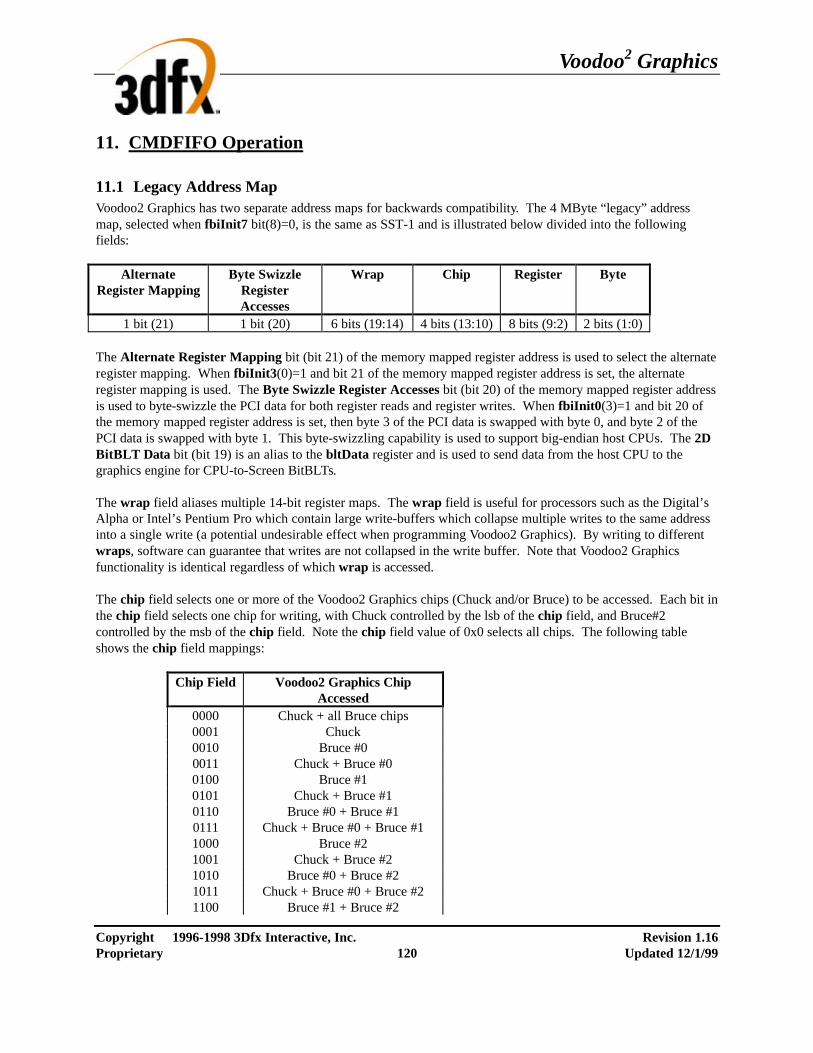
Voodoo2 Graphics
Copyright 1996-1998 3Dfx Interactive, Inc. Revision 1.16 Proprietary 120 Updated 12/1/99
11. CMDFIFO Operation
11.1 Legacy Address Map Voodoo2 Graphics has two separate address maps for backwards compatibility. The 4 MByte “legacy” address map, selected when fbiInit7 bit(8)=0, is the same as SST-1 and is illustrated below divided into the following fields:
Alternate Register Mapping
Byte Swizzle Register Accesses
Wrap Chip Register Byte
1 bit (21) 1 bit (20) 6 bits (19:14) 4 bits (13:10) 8 bits (9:2) 2 bits (1:0) The Alternate Register Mapping bit (bit 21) of the memory mapped register address is used to select the alternate register mapping. When fbiInit3(0)=1 and bit 21 of the memory mapped register address is set, the alternate register mapping is used. The Byte Swizzle Register Accesses bit (bit 20) of the memory mapped register address is used to byte-swizzle the PCI data for both register reads and register writes. When fbiInit0(3)=1 and bit 20 of the memory mapped register address is set, then byte 3 of the PCI data is swapped with byte 0, and byte 2 of the PCI data is swapped with byte 1. This byte-swizzling capability is used to support big-endian host CPUs. The 2D BitBLT Data bit (bit 19) is an alias to the bltData register and is used to send data from the host CPU to the graphics engine for CPU-to-Screen BitBLTs. The wrap field aliases multiple 14-bit register maps. The wrap field is useful for processors such as the Digital’s Alpha or Intel’s Pentium Pro which contain large write-buffers which collapse multiple writes to the same address into a single write (a potential undesirable effect when programming Voodoo2 Graphics). By writing to different wraps, software can guarantee that writes are not collapsed in the write buffer. Note that Voodoo2 Graphics functionality is identical regardless of which wrap is accessed. The chip field selects one or more of the Voodoo2 Graphics chips (Chuck and/or Bruce) to be accessed. Each bit in the chip field selects one chip for writing, with Chuck controlled by the lsb of the chip field, and Bruce#2 controlled by the msb of the chip field. Note the chip field value of 0x0 selects all chips. The following table shows the chip field mappings: Chip Field Voodoo2 Graphics Chip
Accessed 0000 Chuck + all Bruce chips 0001 Chuck 0010 Bruce #0 0011 Chuck + Bruce #0 0100 Bruce #1 0101 Chuck + Bruce #1 0110 Bruce #0 + Bruce #1 0111 Chuck + Bruce #0 + Bruce #1 1000 Bruce #2 1001 Chuck + Bruce #2 1010 Bruce #0 + Bruce #2 1011 Chuck + Bruce #0 + Bruce #2 1100 Bruce #1 + Bruce #2

Voodoo2 Graphics
Copyright 1996-1998 3Dfx Interactive, Inc. Revision 1.16 Proprietary 121 Updated 12/1/99
1101 Chuck + Bruce #1 + Bruce #2 1110 Bruce #0 + Bruce #1 + Bruce #2 1111 Chuck + all Bruce chips Note that Bruce #0 is always connected to Chuck in the system level diagrams of section 3, and Bruce #1 is attached to Bruce #0, etc. By utilizing the different chip fields, software can precisely control the data presented to individual chips which compose the Voodoo2 Graphics graphics subsystem. Note that for reads, the chip field is ignored, and read data is always read from Chuck. The register field selects the register to be accessed. All accesses to the memory mapped registers must be 32-bit accesses. No byte (8-bit) or halfword/short (16-bit) accesses are allowed to the memory mapped registers, so the byte (2-bit) field of all memory mapped register accesses must be 0x0. As a result, to modify individual bits of a 32-bit register, the entire 32-bit word must be written with valid bits in all positions.
11.2 CMDFIFO Address Map Voodoo2 Graphics has two separate address maps for backwards compatibility. When the CMDFIFO is enabled (fbiInit7 bit(8)=1), the “CMDFIFO” address map is selected as shown below:
Address Description 0x0000000-0x01fffff Voodoo2 Graphics memory mapped register set (2 MBytes) 0x0200000-0x03fffff Voodoo2 Graphics CMDFIFO (2 Mbytes) [write-only] 0x0400000-0x07fffff Voodoo2 Graphics linear frame buffer access (4 MBytes, state-based) 0x0800000-0x0ffffff Voodoo2 Graphics texture memory access (8 MBytes) The 2 MByte register address map (range 0x0 - 0x1fffff) accessed when the “CMDFIFO” address map is selected is illustrated below divided into the following fields:
Unused Register Byte 11 bits (20:10). Software must store 0x0. 8 bits (9:2) 2 bits (1:0)
Important Note: When the “CMDFIFO” address map is selected, the only writes that are permitted to the 2 MByte register address map (range 0x0 - 0x1fffff) are writes to the following registers: all fbiInit registers, intrCtrl, backPorch, videoDimensions, dacData, hSync, vSync, maxRgbDelta, hBorder, vBorder, borderColor, and all cmdFifo control registers. Writes to any other register other than the above specified registers will be accepted by the PCI slave controller, but will not be pushed onto the PCI frontend FIFO (effectely these writes will be “dropped”). The 2 MByte CMDFIFO address space is a write-only address space used to store commands very efficiency either in off-screen memory or in internal FIFOs (controlled by fbiInit7 bit(9)). Reads from the CMDFIFO address space return undefined data. The CMDFIFO address space is illustrated below divided into the following fields:
Unused Byte Swizzle CMDFIFO Writes
CMDFIFO Address Byte
2 bits (20:19). Software must store 0x0
1 bit (18) 16 bits (17:2) 2 bits (1:0)
When accessing the CMDFIFO address space, software may set bit(18) of the CMDFIFO address to cause the hardware to byte-swizzle the incoming data.

Voodoo2 Graphics
Copyright 1996-1998 3Dfx Interactive, Inc. Revision 1.16 Proprietary 122 Updated 12/1/99
Important Note: Using the CMDFIFO address space and the CMDFIFO packets described below, most registers can be accessed. Those registers which cannot be accessed through the CMDFIFO transport mechanism are the following: all fbiInit registers, intrCtrl, backPorch, videoDimensions, dacData, hSync, vSync, maxRgbDelta, hBorder, vBorder, borderColor, and all cmdFifo control registers. Writes to these registers must be addressed using the 2 MByte register address map (range 0x0 - 0x1fffff) and not the CMDFIFO address space.
11.3 Command Transport A command FIFO (CMDFIFO) may be established by software within frame buffer memory. Writes to the CMDFIFO address space are performed to build a command buffer, which is then parsed and executed by the accelerator. To accommodate a variety of host CPUs which may issue writes out-of-order (eg. Intel’s Pentium Pro), one of two scenarios will occur: the CMDFIFO resides in local frame buffer memory and software manages the accelerator’s internal CMDFIFO depth register, or the CMDFIFO resides in local frame buffer memory and the accelerator manages the internal CMDFIFO depth register.
If the CMDFIFO resides in local frame buffer memory and software manages the CMDFIFO depth register, software “BUMPS” the internal CMDFIFO depth register after N words have been stored into local frame buffer memory. This allows the CPU to write to the CMDFIFO in any order, flush any pending writes in the CPU’s internal write buffers and core logic chipset’s internal write buffers, then update the accelerator’s depth register. Since writes to the CMDFIFO will be in consecutive order, the CPU’s write buffers will fill and burst into memory more efficiently, than random PCI writes.
If the CMDFIFO resides in frame buffer memory and hardware manages the CMDFIFO depth register, software writes to the frame buffer in consecutive order, the CPU flushes its write buffer in any order to the accelerator. The accelerator counts the number of non written addresses, once consecutive addresses are written, the internal CMDFIFO depth register is updated to the last consecutive written address. Counting unwritten addresses allows the CPU to flush its internal write buffers in any order, but maintains the correct order in the frame buffer memory. Software must manage the circular buffer at the point where the buffer recycles to the beginning. This is done by placing a JMP instruction (CMDFIFO Packet Type 0, Func 100) at the bottom of the fifo to restart at the beginning of the CMDFIFO space.
11.3.1 CMDFIFO Management The CMDFIFO mechanism supports 2 types of fifo management, software and hardware
11.3.1.1 Software Management of CMDFIFO
Software manages the CMDFIFO “emptiness.” The accelerator maintains a read pointer and a depth for the CMDFIFO. Accelerator reads from the CMDFIFO decrement the depth register and increment the read pointer. The accelerator will automatically execute data from the CMDFIFO as long as the internal CMDFIFO depth register is greater than zero. When the CPU is ready to inform the accelerator that more data is available in the CMDFIFO, the CPU writes the number of 32-bit words that have been added to the end of the CMDFIFO. The accelerator then adds the value written by the CPU to the internal depth register. The accelerator’s internal registers define where the circular CMDFIFO exists in frame buffer memory by defining a beginning address for the CMDFIFO and a rollover address. By default, the CMDFIFO internal read pointer is set to the beginning address for the CMDFIFO. Once data is stored in the CMDFIFO (and the internal depth register is incremented by the CPU), the CMDFIFO read pointer will increment as the accelerator parses and executes the CMDFIFO. Before the end of the CMDFIFO is reached, a JMP command back to the beginning must be inserted. The CMDFIFO is thus programmable in size as a circular space from 1 to N 4k byte pages. Software must manage CMDFIFO “fullness” and guarantee that the CMDFIFO does not overflow. On systems like the Intel

Voodoo2 Graphics
Copyright 1996-1998 3Dfx Interactive, Inc. Revision 1.16 Proprietary 123 Updated 12/1/99
Pentium Pro, software must place a fence after the last memory write, but before the write to increase the number of new entries in the CMDFIFO.
11.3.1.2 Hardware Management of CMDFIFO
Hardware manages the CMDFIFO depth. The accelerator maintains a read pointer, write pointer, and depth for the CMDFIFO. Accelerator reads from the CMDFIFO decrement the depth register and increment the read pointer. The accelerator will automatically execute data from the CMDFIFO as long as the internal CMDFIFO depth register is greater than zero. The CPU writes data into the CMDFIFO area in sequential addresses. The accelerator snoops the writes into the CMDFIFO area and examines the addresses, looking for non sequential addresses or “holes.” When the accelerator gathers sequential addresses present in the CMDFIFO, the depth and write pointers are incremented. The accelerator’s internal registers define where the circular CMDFIFO exists in frame buffer memory by defining a beginning address for the CMDFIFO and a rollover address. By default, the CMDFIFO internal read pointer is set to the beginning address for the CMDFIFO. Once data is stored in the CMDFIFO (and the internal depth register is incremented by the CPU), the CMDFIFO read pointer will increment as the accelerator parses and executes the CMDFIFO. Before the end of the CMDFIFO is reached, a JMP command back to the beginning must be inserted. The CMDFIFO is thus programmable in size as a circular space from 1 to N 4k byte pages. Software must manage CMDFIFO “fullness” and guarantee that the CMDFIFO does not overflow. On systems like the Intel Pentium Pro, software must place a fence after the last memory write, but before the first write to the top of the CMDFIFO. Or, put another way (from the perspective of a driver writer): When hole counting is enabled (hardware manages command fifo depth), the memory controller takes special action whenever a write occurs between the command fifo base and the base + size. As writes occur in this region, five variables are fiddled: readPtr, depth, aMin, aMax, and holeCount. As ordered writes happen, both aMin and aMax increment, as does depth and readPtr. In this state, the difference between aMin/aMax and the readPtr is the depth. When the depth is nonzero, the readPtr advances as commands are read from the buffer. When/if an out-of-order write occurs, aMin stops incrementing, but aMax continues to increment as addresses written go up. The readPtr will not pass aMin, so the depth begins to decrement. Once the readPtr has caught up with aMin, the depth sits at zero. If aMax ever has to skip (due to an out-of-order write), the hole count is incremented. As out-of-order data gets written between aMin and aMax, the hole count is decremented. When the holeCount goes to zero, the difference between aMin and aMax is added to the depth, and aMin is set to be the same as aMax. This causes command processing to resume.
11.3.2 CMDFIFO Data All CMDFIFO data packets begin with a 32-bit packet header which defines the data which follows. There are 5 different types of CMDFIFO packet headers. Bits (2:0) of a CMDFIFO packet header define the packet header type. All CMDFIFO packet headers and data must be 32-bit words - byte and 16-bit short writes are not allowed in the CMDFIFO.
11.3.3 CMDFIFO Packet Type 0 CMDFIFO Packet Type 0 is a variable length packet, requiring a minimum single 32-bit word, to a maximum of 2 32-bit words. CMDFIFO Packet Type 0 is used to jump to the beginning of the fifo when the end of the fifo is reached. CMDFIFO Packet Type 0 also supports jumping to a secondary command stream just like a jump subroutine call (jsr instruction), with a CMDFIFO Packet that instructs a return as well. NOP, JSR, RET, and JMP LOCAL FRAME BUFFER functions only require a single 32-bit word CMDFIFO packet, while the JMP AGP function requires a two 32-bit word CMDFIFO packet. Bits 31:29 are reserved and must be written with 0.

Voodoo2 Graphics
Copyright 1996-1998 3Dfx Interactive, Inc. Revision 1.16 Proprietary 124 Updated 12/1/99
CMDFIFO Packet Type 0
31 29 28 6 5 3 2 0 word 0 Reserv Address [24:2] Func 000 word 1 reserved Address [35:25]
Code Function
000 NOP 001 JSR 010 RET 011 JMP LOCAL FRAME BUFFER 100 JMP AGP
11.3.4 CMDFIFO Packet Type 1 CMDFIFO Packet Type 1 is a variable length packet that allows writes to either a common address, or to consecutive addresses, minimum number of words is 2 32-bit words, and maximum number of words is 65536 words. Bits 31:16 define the number of words that follow word 0 of packet type 1, and must be greater than 0. When bit 15 is a 1, data following word 0 in the packet is written in consecutive addresses starting from the register base address defined in bits 14:3. When bit 15 is a 0, data following word 0 is written to the base address. Packet header bits 14:3 define the base address of the packet, see section below. The common use of packet type 1 is host blits.
CMDFIFO Packet Type 1
31 16 15 14 3 2 0 word 0 Number of words inc Register Base (See below) 001 word 1 Data word N Optional Data N
Register Base:
CVG
11 7 Chip field Register Number
11.3.5 CMDFIFO Packet Type 2 CMDFIFO Packet Type 2 is a variable length packet, requiring a minimum of 2 32-bit words, and a maximum of 30 32-bit words for the complete packet. The base address for CMDFIFO Packet Type 2 is defined to be the starting address of the hardware 2D registers. The first 32-bit word of the packet defines individual write enables for up to 29 data words to follow. From LSB o MSB of the mask, a “1” enables the write and a “0” disables the write. The sequence of up to 29 32-bit data words following the mask modify addresses equal to the implied base address plus N where mask[N] equals “1” as N ranges from 0 to 28. The total number of 32-bit data words following the mask is equal to the number of “1”s in the mask. The register mask must not be 0.
CMDFIFO Packet Type 2
31 3 2 0 word 0 2D Register mask 010 word 1 Data

Voodoo2 Graphics
Copyright 1996-1998 3Dfx Interactive, Inc. Revision 1.16 Proprietary 125 Updated 12/1/99
word N Optional Data N
11.3.6 CMDFIFO Packet Type 3 CMDFIFO Packet Type 3 is a variable length packet, requiring a minimum of 3 32-bit words, and a maximum of 16 vertex data groups, where a data group is all the register writes specified in the parameter mask, for the complete packet. It is a requirement that bits 9:6 must be greater than 0. The base address for CMDFIFO Packet Type 3 is defined to be the starting address of the hardware triangle setup registers. The first 32-bit word of the packet defines 16 individual vertex data. Bits 31:29 of word 0 define 0 to 7 dummy fifo entries following the packet type 3 data. The sSetupMode register is written with the data in bits 27:10 of word 0. Bits 9:6 define the number of vertex writes contained in the packet, where the total packet size becomes what is defined in the parameter mask multiplied by the number of vertices. During parsing and execution of a CMDFIFO Packet Type 3, a specific action takes place based on bits 5:3. The sSetupMode register implies that X and Y are present in words 1 and 2. When Bit 28 when set, packed color data follows the X and Y values, otherwise independent red, green, blue, and alpha follow X and Y data. When Smode field is 0, then word 0 defines X, and word 1 defines Y.
Code 000 specifies an independent triangle packet, where an implied sBeginTriCMD is written after 2 sDrawTriCMD’s. The sequence would follow, sBeginTriCMD, sDrawTriCMD, sDrawTriCMD, sBeginTriCMD, until “NumVertex” vertices has been executed.
Code 001 specifies the beginning of a triangle strip, an implicit write to sBeginTriCMD is issued, followed by Num Vertex sDrawTriCMD writes. The sequence would follow, sBeginTriCMD, sDrawTriCMD, sDrawTriCMD, sDrawTriCMD, until “num Vertex” vertices has been executed
Code 010 specifies the a continuance of an existing triangle strip, an implicit write to sDrawTriCMD is performed after one complete vertex has been parsed.
CMDFIFO Packet Type 3
31 29 28 27 22 21 10 9 6 5 3 2 0 word 0 Num PC SMode Parameter Mask Num Vertex CMD 011 word 1 Data word N Optional Data N
Code Command
000 Independent Triangle 001 Start new triangle strip 010 Continue existing triangle strip 011 reserved 1xx reserved
Bit Description sParamMask field 10 Setup Red, Green, and Blue 11 Setup Alpha 12 Setup Z 13 Setup Wb 14 Setup W0 15 Setup S0 and T0 16 Setup W1
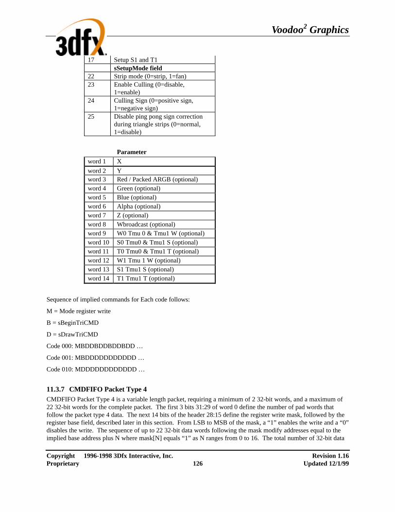
Voodoo2 Graphics
Copyright 1996-1998 3Dfx Interactive, Inc. Revision 1.16 Proprietary 126 Updated 12/1/99
17 Setup S1 and T1 sSetupMode field 22 Strip mode (0=strip, 1=fan) 23 Enable Culling (0=disable,
1=enable) 24 Culling Sign (0=positive sign,
1=negative sign) 25 Disable ping pong sign correction
during triangle strips (0=normal, 1=disable)
Parameter
word 1 X
word 2 Y word 3 Red / Packed ARGB (optional) word 4 Green (optional) word 5 Blue (optional) word 6 Alpha (optional) word 7 Z (optional) word 8 Wbroadcast (optional) word 9 W0 Tmu 0 & Tmu1 W (optional) word 10 S0 Tmu0 & Tmu1 S (optional) word 11 T0 Tmu0 & Tmu1 T (optional) word 12 W1 Tmu 1 W (optional) word 13 S1 Tmu1 S (optional) word 14 T1 Tmu1 T (optional)
Sequence of implied commands for Each code follows:
M = Mode register write
B = sBeginTriCMD
D = sDrawTriCMD
Code 000: MBDDBDDBDDBDD …
Code 001: MBDDDDDDDDDDD …
Code 010: MDDDDDDDDDDDD …
11.3.7 CMDFIFO Packet Type 4 CMDFIFO Packet Type 4 is a variable length packet, requiring a minimum of 2 32-bit words, and a maximum of 22 32-bit words for the complete packet. The first 3 bits 31:29 of word 0 define the number of pad words that follow the packet type 4 data. The next 14 bits of the header 28:15 define the register write mask, followed by the register base field, described later in this section. From LSB to MSB of the mask, a “1” enables the write and a “0” disables the write. The sequence of up to 22 32-bit data words following the mask modify addresses equal to the implied base address plus N where mask[N] equals “1” as N ranges from 0 to 16. The total number of 32-bit data

Voodoo2 Graphics
Copyright 1996-1998 3Dfx Interactive, Inc. Revision 1.16 Proprietary 127 Updated 12/1/99
must have a non zero value.
CMDFIFO Packet Type 4
31 29 28 15 14 3 2 0 word 0 num General Register mask Register Base (See below) 100 word 1 Data word N Optional Data N
Register base:
CVG
11 7 Chip field Register Number
11.3.8 CMDFIFO Packet Type 5 CMDFIFO Packet Type 5 is a variable length packet, requiring a minimum of 3 32-bit words, and a maximum of 2^19 32-bit words for the complete packet Bits 31:30 define linear frame buffer or texture download port Bits 29:26 in word 0 define the byte “disables” for word 2 and are active high (a value of 1 prohibits the byte from being written). Bits 25:22 in word 0 define the byte enables for word N. Data must be in the correct data lane, and the base address must be 32-bit aligned. CMDFIFO Packet Type 5 is used to transfer large consecutive quantities of data from the CPU to the frame buffer or texture memory with proper order with the command stream.
CMDFIFO Packet Type 5
31 30 29 26 25 22 21 2 0 word 0 Space Byte Disable W2 Byte Disable WN Num Words 101 word 1 reserv Base Address [24:0] word 2 Data word N Optional Data N
Code Space
00-01 reserved 10 Linear frame buffer 11 Texture Port

Voodoo2 Graphics
Copyright 1996-1998 3Dfx Interactive, Inc. Revision 1.16 Proprietary 128 Updated 12/1/99
12. Programming Caveats The following is a list of programming guidelines which are detailed elsewhere but may have been overlooked or misunderstood:
12.1 I/O Accesses Voodoo2 Graphics does not support I/O accesses. All I/O accesses to Voodoo2 Graphics are ignored.
12.2 Memory Accesses All Memory accesses to Voodoo2 Graphics registers must be 32-bit word accesses only. Linear frame buffer accesses may be 32-bit or 16-bit accesses, depending upon the linear frame buffer access format specified in lfbMode. Texture memory accesses must be 32-bit word accesses. Byte(8-bit) accesses are not allowed to Voodoo2 Graphics register, linear frame buffer, or texture memory space.
12.3 Determining CVG Idle Condition After certain CVG operations, and specifically after linear frame buffer acceses, there exists a potential deadlock condition between internal CVG state machines which is manifest when determining if the CVG subsystem is idle. To avoid this problem, always issue a NOP command before reading the status register when polling on the CVG busy bit. Also, to avoid asynchronous boundary conditions when determing the idle status, always read CVG inactive in status three times. A sample code segment for determining CVG idle status is as follows: /********************************************************* * CVG_IDLE: * returns 0 if CVG is not idle * returns 1 if CVG is idle *********************************************************/ CVG_IDLE() { ulong j, i; // Make sure CVG state machines are idle PCI_MEM_WR(NOPCMD, 0x0); i = 0; while(1) { j = PCI_MEM_RD(STATUS); if(j & CVG_BUSY) return(0); else i++; if(i > 3) return(1); } }
12.4 Triangle Subpixel Correction Triangle subpixel correction is performed in the on-chip triangle setup unit of Voodoo2 Graphics. When subpixel correction is enabled (fbzColorPath(26)=1), the incoming starting color, depth, and texture coordinate parameters

Voodoo2 Graphics
Copyright 1996-1998 3Dfx Interactive, Inc. Revision 1.16 Proprietary 129 Updated 12/1/99
are all corrected for non-integer aligned starting triangle <x,y> coordinates. The subpixel correction in the triangle setup unit is performed as the starting color, depth, and texture coordinate parameters are read from the PCI FIFO. As a result, the exact data sent from the host CPU is changed to account for subpixel alignments. If a triangle is rendered with subpixel correction enabled, all subsequent triangles must resend starting color, depth, and texture coordinate parameters, otherwise the last triangle’s subpixel corrected starting parameters are subpixel corrected (again!), and incorrect results are generated.
12.5 Loading the internal Color Lookup Table When loading the color lookup table by writing data to clutData, the software video reset bit must be disabled (fbiinit1(8)=0). If the software video reset bit is enabled (fbiinit1(8)=1), the data written to clutData is ignored.

Voodoo2 Graphics
Copyright 1996-1998 3Dfx Interactive, Inc. Revision 1.16 Proprietary 130 Updated 12/1/99
13. Video Timing Voodoo2 Graphics video timing is defined by the hSync, vSync, backPorch, and videoDimensions registers. The following diagram illustrates the video timing parameters of Voodoo2 Graphics:
hBackPorch hBackColor hFrontColor
Act ive Drawing Area
Border Color Area
B lanking Area
vBackPorch
vBackColor
vFrontColor
xWidth
yHeight
hSyncOff
vSyncOff
hSyncOn hSyncOffdac_hsync(active low)
dac_blank(active low)
hBackPorch hBackColor hFrontColorxWidth
B lanking Area B lanking AreaBorderColor Area
BorderColor Area
ActiveV ideo Area
vSyncOn vSyncOffdac_vsync(active low)
dac_blank(active low)
vBackPorch vBackColor vFrontColoryHeight
B lanking Area B lanking AreaBorderColor Area
BorderColor Area
ActiveV ideo Area

Voodoo2 Graphics
Copyright 1996-1998 3Dfx Interactive, Inc. Revision 1.16 Proprietary 131 Updated 12/1/99
The screen resolution is defined in the videoDimensions register. The horizontal screen resolution is specified in the xWidth field of videoDimensions, and the vertical screen resolution is specified in the yHeight field of videoDimensions. The hSync register is used to control the horizontal sync period. The values of hSync are specified in VCLK units, which is the video dot clock. hSyncOn = (Number VCLKs of active horizontal Sync) - 1 hSyncOff = (Number VCLKs of inactive horizontal Sync) - 1 The vSync register is used to control the vertical sync period. The values of vSync are specified in horizontal scan line units. The width of a horizontal scan line is defined by the hSync register. vSyncOn = (Number horizontal scan lines of active vertical Sync) vSyncOff = (Number horizontal scan lines of inactive vertical Sync) The area between the left hand side of the monitor and the border color region, known as the horizontal back porch, is defined by the hBackPorch field in the backPorch register. The register value is specified in VCLK units. hBackPorch = (Number VCLKs of active horizontal back porch Blank) - 2 The horizontal area between the active video region and the blanking area, known as the color border area, is defined by the hBorder register. The register value is specified in VCLK units. Note that no border color area is specified by setting the appropriate fields in hBorder to 0x0. hBackColor = (Number VCLKs of active horizontal color border [left-hand side]) hFrontColor = (Number VCLKs of active horizontal color border [right-hand side]) The area between the right hand side of the monitor and the border color region, known as the horizontal front porch, is inferred from the horizontal Sync, the horizontal display resolution information, and the right hand side horizontal color border information. The area between the top of the monitor and the color border region, known as the vertical back porch, is defined by the vBackPorch field in the backPorch register. The register value is specified in horizontal scan line units. vBackPorch = (Number Horizontal Scan Lines of active vertical back porch Blank) The vertical area between the active video region and the blanking area, known as the color border area, is defined by the vBorder register. The register value is specified in horizontal scan line units. Note that no border color area is specified by setting the appropriate fields in vBorder to 0x0. vBackColor = (Number Horizontal Scan Lines of vertical color border [top]) vFrontColor = (Number Horizontal Scan Lines of vertical color border [bottom]) The area between the bottom of the monitor and the border color region, known as the vertical front porch, is inferred from the vertical Sync, the vertical display resolution information and the bottom vertical color border information. When generating PCI interrupts, the status of the internal vSyncOff counter is compared to bits(27:16) of the pciInterrupt register. Note that the value of the internal vSyncOff counter may be probed in software by reading the vRetrace register.

Voodoo2 Graphics
Copyright 1996-1998 3Dfx Interactive, Inc. Revision 1.16 Proprietary 132 Updated 12/1/99
14. Revision History
1.10 • First draft given to Sega 01Ap97
1.11
• Added more explanation to CMDFIFO packet types • CMDFIFO packet type 0 no longer has word padding capability in bits (31:29) • Added bit to enable bursting of consecutive texture memory writes across FT Bus in fbiInit7 bit(27) • Renamed fbiTriangles register to fbiTrianglesOut register and implemented in Alpha version.
Moved fbiTrianglesOut register to 0x25c. Added bit in nopCMD to separately clear fbiTrianglesOut.
• Added fbiSwapHistory register at address 0x258 • Implemented interrupts in Alpha version (implemented intrCtrl and userIntrCMD registers).
USERINTERRUPTs now have separate control of whether to generate an interrupt, and whether to wait for the USERINTERRUPT to be cleared before continuing processing the command stream. Added interrupt control bits in PCI configuration register initEnable bits(21:20).
• Changed tiling algorithm from 64x16 tiles to 32x32 tiles. Added bit 30 in fbiInit6 to add another bit to the tilesInX parameter used in the XY-to-Row/Col memory mapping algorithm. Changed description of bltXYStrides register to account for more tiles in 32x32 algorithm.
• Added initEnable bit(22) to enable NAND tree testing • Added initEnable bits(31:23) to enable SLI address snooping
1.12
• Changed spec to indicate than when fb_addr_b[1]=1 at the deassertion of pci_rst, the default value of the memory base address is 0x10000008.
• Fixes typos in triangle setup register descriptions • Changed name from “Console Voodoo Graphics” to “Voodoo2 Graphics”
1.13
• Added siProcess register description • Fixed description of clutData register to be non-pipelined, FIFO’ed • Fixed typos in fbiInit regiseters • Fixed description of bits(10:9) in PCI status configuration register. • Fixed typo in Section 9 describing location of linear frame buffer address space. • Changed bit descriptions in fbiInit5 to account for new clock buffering schemes on GPIO_1 and to
include triangle raster unit CYA bits. Removed references to interleaved video mode in fbiInit5. 1.14
• Changed byte “enables” to byte “disables” for description of CMDFIFO packet type 5 • Fixed definition of fbiInit5 bit(13)
1.15
• Changed default value of PCI configuration register Interrupt_line to 0x0 • Fixed typo in tiled memory mapper algorithm in bltXYStrides register definition • Added definition of fbiInit4[31:29] for Chuck revision 5 to control video clock delay settings