vout gnd 42 57 nc t 3 xposed 6 4 5 - diodes incorporated · soft start-up and shutdown along with v...
TRANSCRIPT
AP2303 Document number: DS36546 Rev. 3 - 2
1 of 15 www.diodes.com
September 2014 © Diodes Incorporated
AP2303
A Product Line of
Diodes Incorporated
NE
W P
RO
DU
CT
DDR BUS TERMINATION REGULATOR
Description
The AP2303 is a low dropout linear regulator to generate termination voltage of DDR-SDRAM system. The regulator can source or sink up to 1.75A current continuously. The output voltage is regulated to track
tightly with the reference voltage (1/2VDDQ) within ±10mV. The AP2303 supports soft start-up when used to turn on the VCNTL and VREFEN. It integrates a shutdown circuit that will be triggered once the voltage of VIN, VCNTL or VREFEN falls below a certain value. AP2303 features over temperature protection and current limit protection for both source and sink. AP2303 is available in packages of SOIC-8 and PSOP-8.
Features
Support DDR-II (VTT=0.9V), DDR-III (VTT=0.75V), DDR-IIIL
(VTT=0.675V), DDR-IV (VTT=0.6V) Application
Source and Sink up to 1.75A Current
Output Voltage Accuracy Over Full Load: ±2% (Max.)
Soft Start-up and Shutdown along with VIN, VCNTL and VREFEN
Rising and Shutdown along with VIN, VCNTL and VREFEN Dropping
Flexible Output by 2 External Resistors
Requires Minimum 10µF Output Ceramic Capacitor for Application
Current Limit Protection for Both Source and Sink
OTSD Protection
Totally Lead-Free & Fully RoHS Compliant (Notes 1 & 2)
Halogen and Antimony Free. “Green” Device (Note 3)
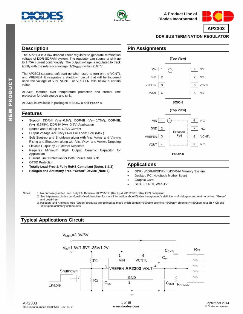
Pin Assignments
(Top View)
SOIC-8
(Top View)
PSOP-8
Applications
DDR-II/DDR-III/DDR-IIIL/DDR-IV Memory System
Desktop PC, Notebook Mother Board
Graphic Card
STB, LCD-TV, Web-TV
Notes: 1. No purposely added lead. Fully EU Directive 2002/95/EC (RoHS) & 2011/65/EU (RoHS 2) compliant. 2. See http://www.diodes.com/quality/lead_free.html for more information about Diodes Incorporated’s definitions of Halogen- and Antimony-free, "Green" and Lead-free. 3. Halogen- and Antimony-free "Green” products are defined as those which contain <900ppm bromine, <900ppm chlorine (<1500ppm total Br + Cl) and <1000ppm antimony compounds.
Typical Applications Circuit
VIN
VCNTL
VREFEN AP2303 VOUT
GND
RTT
COUT
VCNTL=3.3V/5V
R1
R2CSS
CCNTL
CIN
VIN=1.8V/1.5V/1.35V/1.2V
RDUMMY
1
4
2
3
6
Shutdown
Enable
VIN
GND
VREFEN
VOUT
NC
NC
VCNTL
NC
1
2
3
4
8
7
6
5
1
2
3
4
8
7
6
5VOUT
GND
VIN NC
NC
VCNTL
NC
VREFEN
Exposed
Pad

AP2303 Document number: DS36546 Rev. 3 - 2
2 of 15 www.diodes.com
September 2014 © Diodes Incorporated
AP2303
A Product Line of
Diodes Incorporated
NE
W P
RO
DU
CT
Pin Descriptions
Pin Number Pin Name Function
1 VIN Unregulated input supply. A small 10µF MLCC should be connected from this pin to GND.
2 GND Ground
3 VREFEN Reference voltage input and active low shutdown control pin. Pulling the pin to ground turns off
device by BJT or FET. When it is released, a soft-start will take for about 0.1ms.
4 VOUT Regulated voltage output. A minimum of 10µF ceramic capacitor to ground is required to assure
stability.
5, 7, 8 NC No Connection
6 VCNTL VCNTL supplies the internal control circuitry and provides the drive voltage.
– Exposed Pad The exposed pad should be connected to ground copper for better heat dissipation performance.
Functional Block Diagram
Enable
Thermal
Shutdown
Current Limit
Error
Amplifier
and
Soft Start
Power On
Reset
VCNTL
EN
VREF
OTSDPOR
VIN
VREFEN VOUT
GND
6
3
1
4
2

AP2303 Document number: DS36546 Rev. 3 - 2
3 of 15 www.diodes.com
September 2014 © Diodes Incorporated
AP2303
A Product Line of
Diodes Incorporated
NE
W P
RO
DU
CT
Absolute Maximum Ratings (Note 4)
Symbol Parameter Rating Unit
VIN Power Input Voltage -0.3 to 6 V
VCNTL Control Input Voltage -0.3 to 6 V
VREFEN Reference Input Voltage -0.3 to 6 V
TSTG Storage Temperature +150 °C
TJ Junction Temperature +150 °C
TLEAD Lead Temperature (Soldering, 10sec) +260 °C
θJA Thermal Resistance (Junction to Ambient) (Note 5)
PSOP-8 80
°C/W
SOIC-8 110
θJC Thermal Resistance (Junction to Case)
PSOP-8 38
°C/W
SOIC-8 50
ESD ESD (Human Body Model) 2000 V
ESD ESD (Machine Model) 200 V
Notes: 4. Stresses greater than those listed under “Absolute Maximum Ratings” may cause permanent damage to the device. These are stress ratings only, and
functional operation of the device at these or any other conditions beyond those indicated under “Recommended Operating Conditions” is not implied.
Exposure to “Absolute Maximum Ratings” for extended periods may affect device reliability.
5. θJA is measured with the component mounted on a 2-Layer FR-4 board with 2.54cm*2.54cm thermal sink pad in free air.
Recommended Operating Conditions
Symbol Parameter Min Max Unit
VCNTL Control Input Voltage (Note 6) 3.0 5.5 V
VIN Power Input Voltage 1.2 5.5 V
VREFEN Reference Input Voltage 0.6 VCNTL-2.2 V
TJ Operating Junction Temperature Range -40 +125 °C
TA Operating Ambient Temperature Range -40 +85 °C
Note 6: Keep VCNTL ≥ VIN in operation power on and power off sequences.
AP2303 Document number: DS36546 Rev. 3 - 2
4 of 15 www.diodes.com
September 2014 © Diodes Incorporated
AP2303
A Product Line of
Diodes Incorporated
NE
W P
RO
DU
CT
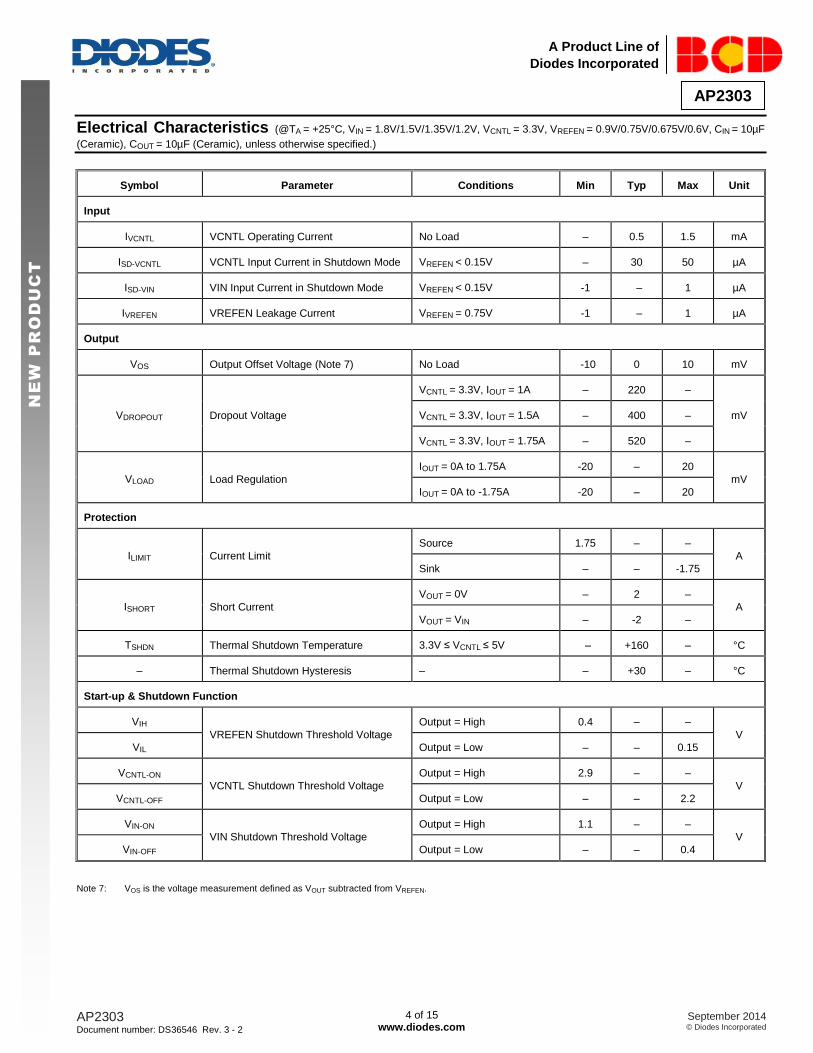
Electrical Characteristics (@TA = +25°C, VIN = 1.8V/1.5V/1.35V/1.2V, VCNTL = 3.3V, VREFEN = 0.9V/0.75V/0.675V/0.6V, CIN = 10µF
(Ceramic), COUT = 10µF (Ceramic), unless otherwise specified.)
Symbol Parameter Conditions Min Typ Max Unit
Input
IVCNTL VCNTL Operating Current No Load – 0.5 1.5 mA
ISD-VCNTL VCNTL Input Current in Shutdown Mode VREFEN < 0.15V – 30 50 µA
ISD-VIN VIN Input Current in Shutdown Mode VREFEN < 0.15V -1 – 1 µA
IVREFEN VREFEN Leakage Current VREFEN = 0.75V -1 – 1 µA
Output
VOS Output Offset Voltage (Note 7) No Load -10 0 10 mV
VDROPOUT Dropout Voltage
VCNTL = 3.3V, IOUT = 1A – 220 –
mV VCNTL = 3.3V, IOUT = 1.5A – 400 –
VCNTL = 3.3V, IOUT = 1.75A – 520 –
VLOAD Load Regulation
IOUT = 0A to 1.75A -20 – 20
mV
IOUT = 0A to -1.75A -20 – 20
Protection
ILIMIT Current Limit
Source 1.75 – –
A
Sink – – -1.75
ISHORT Short Current
VOUT = 0V – 2 –
A
VOUT = VIN – -2 –
TSHDN Thermal Shutdown Temperature 3.3V ≤ VCNTL ≤ 5V – +160 – °C
– Thermal Shutdown Hysteresis – – +30 – °C
Start-up & Shutdown Function
VIH
VREFEN Shutdown Threshold Voltage
Output = High 0.4 – –
V
VIL Output = Low – – 0.15
VCNTL-ON
VCNTL Shutdown Threshold Voltage
Output = High 2.9 – –
V
VCNTL-OFF Output = Low – – 2.2
VIN-ON
VIN Shutdown Threshold Voltage
Output = High 1.1 – –
V
VIN-OFF Output = Low – – 0.4
Note 7: VOS is the voltage measurement defined as VOUT subtracted from VREFEN.

AP2303 Document number: DS36546 Rev. 3 - 2
5 of 15 www.diodes.com
September 2014 © Diodes Incorporated
AP2303
A Product Line of
Diodes Incorporated
NE
W P
RO
DU
CT
Performance Characteristics
Output Offset Voltage vs. Ambient Temperature Dropout Voltage vs. Output Current
Source Current Limit vs. VCNTL Input Voltage Sink Current Limit vs. VCNTL Input Voltage
VCNTL Operating Input Current vs. Ambient Temperature VCNTL Standby Current vs. Ambient Temperature
-40 -20 0 20 40 60 80 100 1200.0
0.5
1.0
1.5
2.0
2.5
3.0
Ou
tpu
t O
ffse
t V
olta
ge
(m
V)
Ambient Temperature (oC)
0.00 0.25 0.50 0.75 1.00 1.25 1.50 1.750
50
100
150
200
250
300
350
400
450
500
550
600
650
700
Dro
po
ut V
olta
ge
(m
V)
Output Current (A)
VCNTL
=3.3V
TA=-40
oC
TA=25
oC
TA=85
oC
3.0 3.2 3.4 3.6 3.8 4.0 4.2 4.4 4.6 4.8 5.0
1.0
1.2
1.4
1.6
1.8
2.0
2.2
2.4
2.6
2.8
3.0
3.2
3.4
3.6
3.8
4.0
Sou
rce C
urr
en
t L
imit (
A)
VCNTL Input Voltage (V)
VIN
=1.5V, VREFEN
=0.75V
TA=-40
oC
TA=25
oC
TA=85
oC
3.0 3.2 3.4 3.6 3.8 4.0 4.2 4.4 4.6 4.8 5.0
-1.0
-1.2
-1.4
-1.6
-1.8
-2.0
-2.2
-2.4
-2.6
-2.8
-3.0
-3.2
-3.4
-3.6
-3.8
-4.0
Sin
k C
urr
en
t L
imit (
A)
VCNTL Input Voltage (V)
VIN
=1.5V, VREFEN
=0.75V
TA=-40
oC
TA=25
oC
TA=85
oC
-40 -20 0 20 40 60 80 100 120400
450
500
550
600
650
700
VC
NT
L O
pe
ratin
g In
pu
t C
urr
en
t (
A)
Ambient Temperature (oC)
VCNTL
=5V
-40 -20 0 20 40 60 80 100 120
10
15
20
25
30
35
40
VC
NT
L S
tan
db
y C
urr
en
t (
A)
Ambient Temperature (oC)
VCNTL
=5V, VREFEN
=0.15V
AP2303 Document number: DS36546 Rev. 3 - 2
6 of 15 www.diodes.com
September 2014 © Diodes Incorporated
AP2303
A Product Line of
Diodes Incorporated
NE
W P
RO
DU
CT
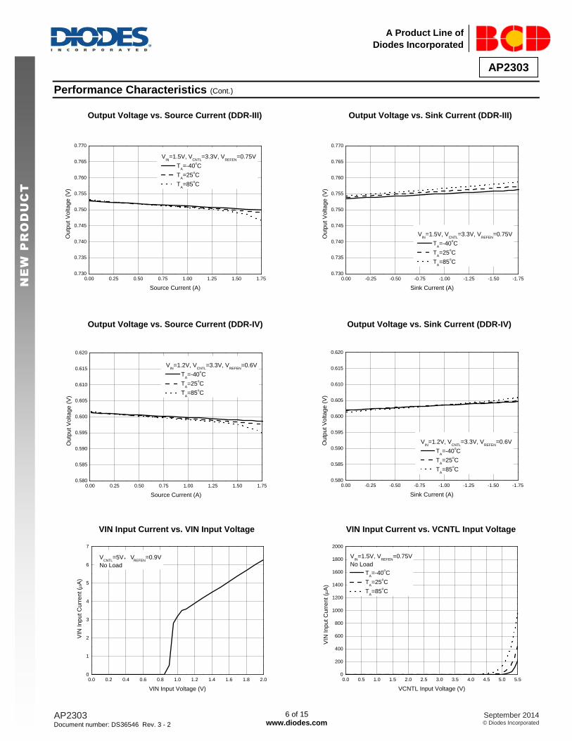
Performance Characteristics (Cont.)
Output Voltage vs. Source Current (DDR-III) Output Voltage vs. Sink Current (DDR-III)
Output Voltage vs. Source Current (DDR-IV) Output Voltage vs. Sink Current (DDR-IV)
VIN Input Current vs. VIN Input Voltage VIN Input Current vs. VCNTL Input Voltage
0.00 0.25 0.50 0.75 1.00 1.25 1.50 1.750.730
0.735
0.740
0.745
0.750
0.755
0.760
0.765
0.770
Ou
tpu
t V
olta
ge
(V
)
Source Current (A)
VIN
=1.5V, VCNTL
=3.3V, VREFEN
=0.75V
TA=-40
oC
TA=25
oC
TA=85
oC
0.00 -0.25 -0.50 -0.75 -1.00 -1.25 -1.50 -1.750.730
0.735
0.740
0.745
0.750
0.755
0.760
0.765
0.770
Ou
tpu
t V
olta
ge
(V
)
Sink Current (A)
VIN
=1.5V, VCNTL
=3.3V, VREFEN
=0.75V
TA=-40
oC
TA=25
oC
TA=85
oC
0.00 0.25 0.50 0.75 1.00 1.25 1.50 1.750.580
0.585
0.590
0.595
0.600
0.605
0.610
0.615
0.620
Ou
tpu
t V
olta
ge
(V
)
Source Current (A)
VIN
=1.2V, VCNTL
=3.3V, VREFEN
=0.6V
TA=-40
oC
TA=25
oC
TA=85
oC
0.00 -0.25 -0.50 -0.75 -1.00 -1.25 -1.50 -1.750.580
0.585
0.590
0.595
0.600
0.605
0.610
0.615
0.620
Ou
tpu
t V
olta
ge
(V
)
Sink Current (A)
VIN
=1.2V, VCNTL
=3.3V, VREFEN
=0.6V
TA=-40
oC
TA=25
oC
TA=85
oC
0.0 0.2 0.4 0.6 0.8 1.0 1.2 1.4 1.6 1.8 2.00
1
2
3
4
5
6
7
VIN
In
pu
t C
urr
en
t (
A)
VIN Input Voltage (V)
VCNTL
=5V,VREFEN
=0.9V
No Load
0.0 0.5 1.0 1.5 2.0 2.5 3.0 3.5 4.0 4.5 5.0 5.50
200
400
600
800
1000
1200
1400
1600
1800
2000
VIN
In
pu
t C
urr
en
t (
A)
VCNTL Input Voltage (V)
VIN
=1.5V, VREFEN
=0.75V
No Load
TA=-40
oC
TA=25
oC
TA=85
oC

AP2303 Document number: DS36546 Rev. 3 - 2
7 of 15 www.diodes.com
September 2014 © Diodes Incorporated
AP2303
A Product Line of
Diodes Incorporated
NE
W P
RO
DU
CT
Performance Characteristics (Cont.)
Source Load Transient (DDR-III) Sink Load Transient (DDR-III)
(CIN=COUT=10µF, IOUT=0A to 1.75A, (CIN=COUT=10µF, IOUT=0A to -1.75A,
VIN=1.5V, VREFEN=0.75V, VCNTL=3.3V) VIN=1.5V, VREFEN=0.75V, VCNTL=3.3V)
Source Load Transient (DDR-IV) Sink Load Transient (DDR-IV)
(CIN=COUT=10µF, IOUT=0A to 1.75A, (CIN=COUT=10µF, IOUT=0A to -1.75A,
VIN=1.2V, VREFEN=0.6V, VCNTL=3.3V) VIN=1.2V, VREFEN=0.6V, VCNTL=3.3V)
VREFEN Power On VREFEN Power Off
(CIN=COUT=10µF, RLOAD=5Ω, VCNTL=5V) (CIN=COUT=10µF, RLOAD=5Ω, VCNTL=5V)
VOUT
20mV/div
IOUT
1A/div
Time 100µs/div
VOUT 20mV/div
IOUT 1A/div
Time 100µs/div
VIN 500mV/div
VREFEN
50mV/div
VREFEN
50mV/div
VIN 500mV/div
VOUT
20mV/div
IOUT 1A/div
Time 100µs/div
VOUT
20mV/div
IOUT 1A/div
Time 100µs/div
VREFEN
50mV/div
VIN 500mV/div
VIN 500mV/div
VREFEN
50mV/div
VREFEN
500mV/div IOUT
200mA/div
Time 100µs/div
VREFEN
500mV/div
IOUT 200mA/div
Time 100µs/div
VIN
1V/div
VOUT 500mV/div
VOUT 500mV/div
VIN 1V/div
AP2303 Document number: DS36546 Rev. 3 - 2
8 of 15 www.diodes.com
September 2014 © Diodes Incorporated
AP2303
A Product Line of
Diodes Incorporated
NE
W P
RO
DU
CT
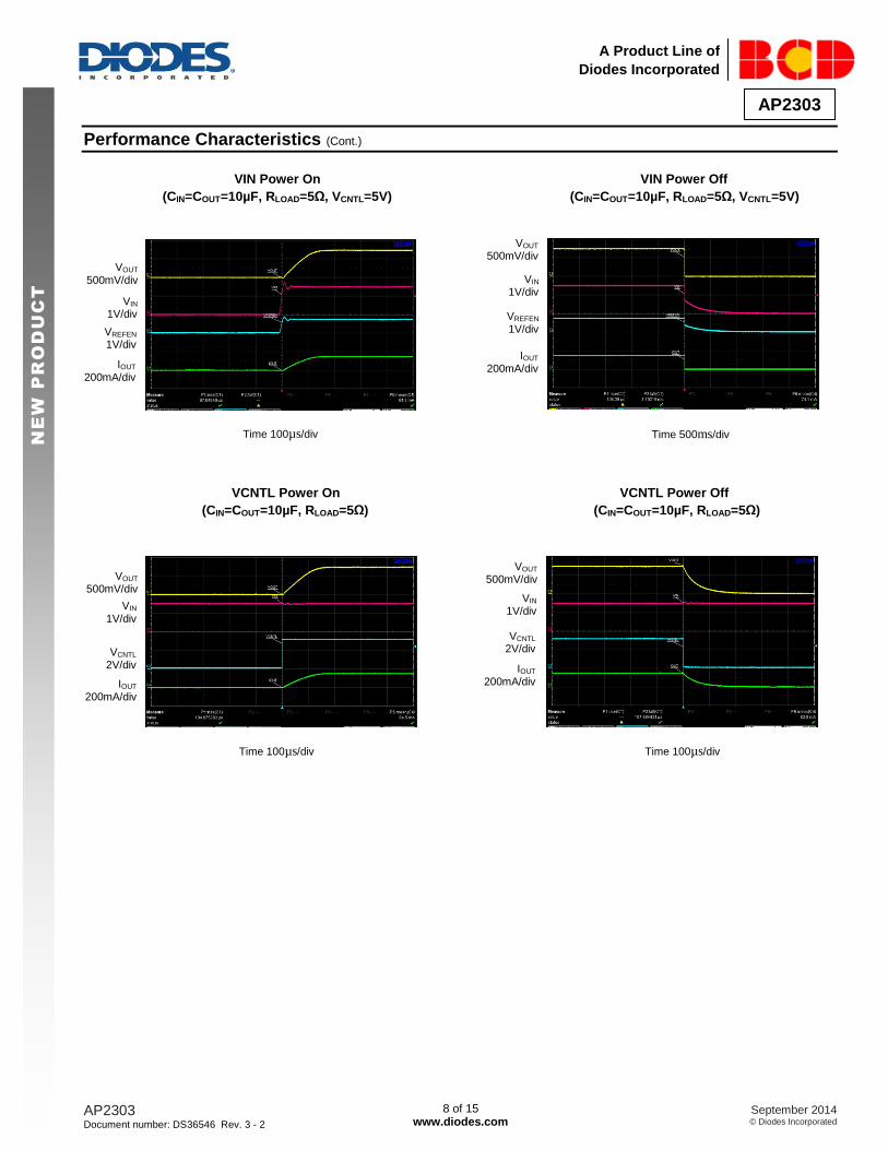
Performance Characteristics (Cont.)
VIN Power On VIN Power Off
(CIN=COUT=10µF, RLOAD=5Ω, VCNTL=5V) (CIN=COUT=10µF, RLOAD=5Ω, VCNTL=5V)
VCNTL Power On VCNTL Power Off
(CIN=COUT=10µF, RLOAD=5Ω) (CIN=COUT=10µF, RLOAD=5Ω)
VOUT
500mV/div
VIN 1V/div
VREFEN 1V/div
IOUT
200mA/div
VOUT 500mV/div
VIN 1V/div
VREFEN
1V/div
IOUT
200mA/div
Time 100µs/div Time 500ms/div
VOUT 500mV/div
VIN
1V/div
VCNTL 2V/div
IOUT
200mA/div
VOUT 500mV/div
VIN 1V/div
VCNTL 2V/div
IOUT
200mA/div
Time 100µs/div Time 100µs/div

AP2303 Document number: DS36546 Rev. 3 - 2
9 of 15 www.diodes.com
September 2014 © Diodes Incorporated
AP2303
A Product Line of
Diodes Incorporated
NE
W P
RO
DU
CT
Application Information
1. Input Capacitor
The input capacitor of VIN should be placed to VIN pin as close as possible. Use a low ESR, 10µF or larger MLCC capacitor to provide surge
current during load transient.
The input capacitor for VCNTL is recommended to be 0.47µF or larger to decouple the supply voltage of AP2303’s control circuitry.
2. Output Capacitor
The output capacitor is recommended with a 10µF or higher MLCC capacitor which will be sufficient at full temperature range. An aluminum
electrolytic capacitor with low ESR also should be larger than 10µF. The output capacitor should be placed to VOUT pin as close as possible.
3. Reference Voltage
A reference voltage is applied to the VREFEN pin by a resistor divider between VIN and GND pins. And a 0.1µF to 1µF bypass capacitor is
preferred to form a low-pass filter to reduce the noise from VIN. More capacitance and large resistance will increase the start-up time after VIN
power-up.
4. Thermal Consideration
There’s an internal thermal protection circuitry of AP2303 to protect device during overload conditions. For continuous operation, make sure not to
exceed the operating junction temperature range of +125°C. The power dissipation definition in device is:
PD=(VIN - VOUT)xIOUT+VINxIQ
The maximum power dissipation depends on the thermal resistance of IC package, PCB layout and the surrounding airflow. The maximum power
dissipation can also be calculated as:
PD(MAX) = (TJ(MAX)-TA)/θJA
The maximum power dissipation for PSOP-8 package at TA = +25°C can be calculated as:
PD(MAX) = (125°C-25°C) / (80°C/W) = 1.25W

AP2303 Document number: DS36546 Rev. 3 - 2
10 of 15 www.diodes.com
September 2014 © Diodes Incorporated
AP2303
A Product Line of
Diodes Incorporated
NE
W P
RO
DU
CT
Ordering Information
AP2303 XX XX – XX
PackingPackageProduct Name
TR : Tape & ReelM : SOIC-8 G1 : Green
RoHS/Green
MP : PSOP-8
Package Temperature Range Part Number Marking ID Packing
SOIC-8
-40 to +85C
AP2303MTR-G1 2303M-G1 4000/Tape & Reel
PSOP-8 AP2303MPTR-G1 2303MP-G1 4000/Tape & Reel
Marking Information (1) SOIC-8
(Top View)
(2) PSOP-8
(Top View)
First and Second Lines: Logo and Marking ID Third Line: Date Code Y: Year WW: Work Week of Molding A: Assembly House Code XX: 7
th and8
th Digits of Batch No.
2303M -G1 YWWAXX
2303MP -G1 YWWAXX
First and Second Lines: Logo and Marking ID Third Line: Date Code Y: Year WW: Work Week of Molding A: Assembly House Code XX: 7
th and 8
th Digits of Batch No.
AP2303 Document number: DS36546 Rev. 3 - 2
11 of 15 www.diodes.com
September 2014 © Diodes Incorporated
AP2303
A Product Line of
Diodes Incorporated
NE
W P
RO
DU
CT
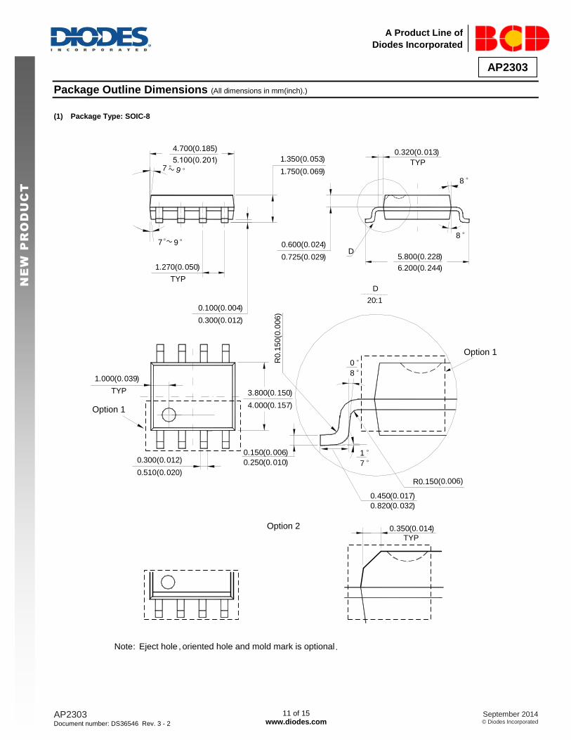
Package Outline Dimensions (All dimensions in mm(inch).)
(1) Package Type: SOIC-8
0°
8°
1°
7°
R0.150(0.006)
R0.1
50(0
.006)
1.000(0.039)
0.300(0.012)
0.510(0.020)
1.350(0.053)
1.750(0.069)
0.100(0.004)
0.300(0.012)
3.800(0.150)
4.000(0.157)
7°
7°
20:1
D
1.270(0.050)
TYP
0.150(0.006)
0.250(0.010)
8°
D5.800(0.228)
6.200(0.244)
0.600(0.024)
0.725(0.029)
0.320(0.013)
8°
0.450(0.017)
0.820(0.032)
4.700(0.185)
5.100(0.201)
Note: Eject hole , oriented hole and mold mark is optional.
Option 1
Option 1
Option 2 0.350(0.014)
TYP
TYP
TYP9°~
9°~
AP2303 Document number: DS36546 Rev. 3 - 2
12 of 15 www.diodes.com
September 2014 © Diodes Incorporated
AP2303
A Product Line of
Diodes Incorporated
NE
W P
RO
DU
CT
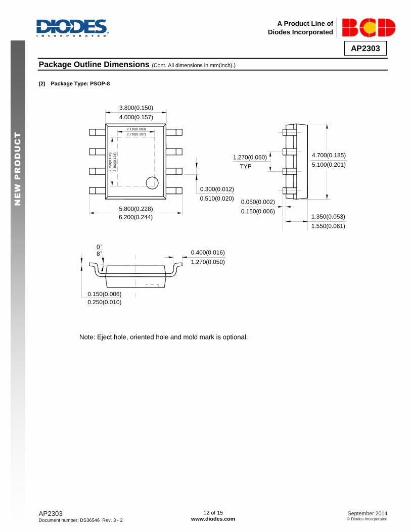
Package Outline Dimensions (Cont. All dimensions in mm(inch).)
(2) Package Type: PSOP-8
8°
5.800(0.228)
6.200(0.244)
1.270(0.050)
0.400(0.016)
3.800(0.150)
4.000(0.157)
0.510(0.020)0.050(0.002)
0.150(0.006)
4.700(0.185)1.270(0.050)
TYP
0°
0.250(0.010)
0.150(0.006)
1.350(0.053)
1.550(0.061)
2.110(0.083)
2.710(0.107)
2.7
50(0
.10
8)
3.4
02(0
.13
4)
5.100(0.201)
Note: Eject hole, oriented hole and mold mark is optional.
0.300(0.012)

AP2303 Document number: DS36546 Rev. 3 - 2
13 of 15 www.diodes.com
September 2014 © Diodes Incorporated
AP2303
A Product Line of
Diodes Incorporated
NE
W P
RO
DU
CT
Suggested Pad Layout
(1) Package Type: SOIC-8
Grid
placement
courtyard
ZG
Y
E X
Dimensions Z
(mm)/(inch)
G
(mm)/(inch)
X
(mm)/(inch)
Y
(mm)/(inch)
E
(mm)/(inch)
Value 6.900/0.272 3.900/0.154 0.650/0.026 1.500/0.059 1.270/0.050

AP2303 Document number: DS36546 Rev. 3 - 2
14 of 15 www.diodes.com
September 2014 © Diodes Incorporated
AP2303
A Product Line of
Diodes Incorporated
NE
W P
RO
DU
CT
Suggested Pad Layout (Cont.)
(2) Package Type: PSOP-8
G
E X
X1
Y
Y1Z
Dimensions Z
(mm)/(inch)
G
(mm)/(inch)
X
(mm)/(inch)
Y
(mm)/(inch)
X1
(mm)/(inch)
Y1
(mm)/(inch)
E
(mm)/(inch)
Value 6.900/0.272 3.900/0.154 0.650/0.026 1.500/0.059 3.600/0.142 2.700/0.106 1.270/0.050
AP2303 Document number: DS36546 Rev. 3 - 2
15 of 15 www.diodes.com
September 2014 © Diodes Incorporated
AP2303
A Product Line of
Diodes Incorporated
NE
W P
RO
DU
CT
IMPORTANT NOTICE DIODES INCORPORATED MAKES NO WARRANTY OF ANY KIND, EXPRESS OR IMPLIED, WITH REGARDS TO THIS DOCUMENT, INCLUDING, BUT NOT LIMITED TO, THE IMPLIED WARRANTIES OF MERCHANTABILITY AND FITNESS FOR A PARTICULAR PURPOSE (AND THEIR EQUIVALENTS UNDER THE LAWS OF ANY JURISDICTION). Diodes Incorporated and its subsidiaries reserve the right to make modifications, enhancements, improvements, corrections or other changes without further notice to this document and any product described herein. Diodes Incorporated does not assume any liability arising out of the application or use of this document or any product described herein; neither does Diodes Incorporated convey any license under its patent or trademark rights, nor the rights of others. Any Customer or user of this document or products described herein in such applications shall assume all risks of such use and will agree to hold Diodes Incorporated and all the companies whose products are represented on Diodes Incorporated website, harmless against all damages. Diodes Incorporated does not warrant or accept any liability whatsoever in respect of any products purchased through unauthorized sales channel. Should Customers purchase or use Diodes Incorporated products for any unintended or unauthorized application, Customers shall indemnify and hold Diodes Incorporated and its representatives harmless against all claims, damages, expenses, and attorney fees arising out of, directly or indirectly, any claim of personal injury or death associated with such unintended or unauthorized application. Products described herein may be covered by one or more United States, international or foreign patents pending. Product names and markings noted herein may also be covered by one or more United States, international or foreign trademarks. This document is written in English but may be translated into multiple languages for reference. Only the English version of this document is the final and determinative format released by Diodes Incorporated.
LIFE SUPPORT Diodes Incorporated products are specifically not authorized for use as critical components in life support devices or systems without the express written approval of the Chief Executive Officer of Diodes Incorporated. As used herein: A. Life support devices or systems are devices or systems which: 1. are intended to implant into the body, or
2. support or sustain life and whose failure to perform when properly used in accordance with instructions for use provided in the labeling can be reasonably expected to result in significant injury to the user.
B. A critical component is any component in a life support device or system whose failure to perform can be reasonably expected to cause the failure of the life support device or to affect its safety or effectiveness. Customers represent that they have all necessary expertise in the safety and regulatory ramifications of their life support devices or systems, and acknowledge and agree that they are solely responsible for all legal, regulatory and safety-related requirements concerning their products and any use of Diodes Incorporated products in such safety-critical, life support devices or systems, notwithstanding any devices- or systems-related information or support that may be provided by Diodes Incorporated. Further, Customers must fully indemnify Diodes Incorporated and its representatives against any damages arising out of the use of Diodes Incorporated products in such safety-critical, life support devices or systems. Copyright © 2014, Diodes Incorporated www.diodes.com