vref ref vref vcc v vcc vcc- 5vreg 5v c5v 3.6v to 35v
TRANSCRIPT
○Product structure:Silicon monolithic integrated circuit ○This product has no designed protection against radioactive rays
1/25 TSZ22111・14・001 © 2015 ROHM Co., Ltd. All rights reserved. TSZ02201-0Q3Q0AJ00470-1-2
06.Nov.2015 Rev.001
www.rohm.com
3.6V to 35V Input 1ch Buck Controller BD9845FV
General Description BD9845FV is a switching regulator controller that uses pulse width modulation. This IC can be used for step-down DC/DC converter applications. BD9845FV is available in a compact package that is optimum for compact power supplies of many kinds of equipment.
Features Operates up to (VCC=35V) Contains FET Driver Circuit (Step-Down Circuit 1
output). REG Output Circuit (2.5V) are contained. Built-In Over Current Protect Adjustable Soft Start and Pause Period. Three modes of Standby, Master, and Slave can be
Switched. (ICCS = 0 µA typ during standby) ON/OFF control is enabled independently for each
channel. (DT terminal)
Applications LCD, PDP, PC, AV, Printer, DVD, Projector TV, Fax, Copy Machine, Measuring Instrument, etc
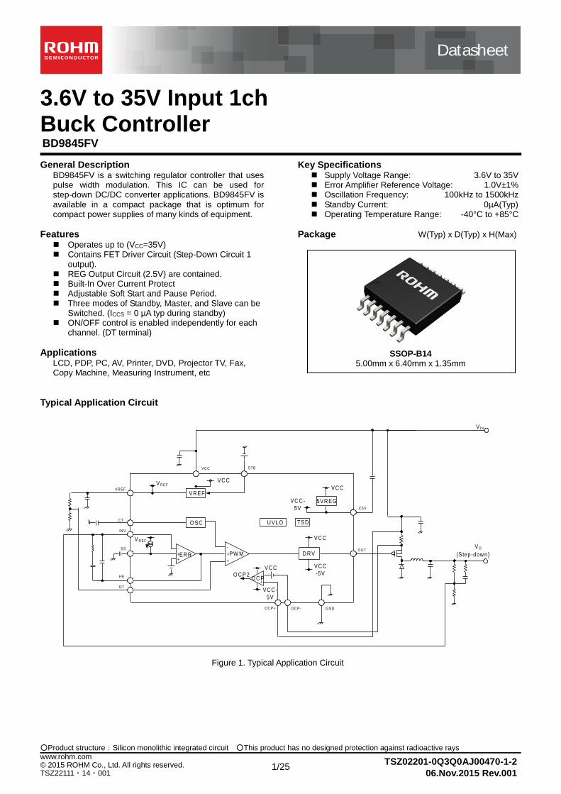
Typical Application Circuit
Key Specifications Supply Voltage Range: 3.6V to 35V Error Amplifier Reference Voltage: 1.0V±1% Oscillation Frequency: 100kHz to 1500kHz Standby Current: 0µA(Typ) Operating Temperature Range: -40°C to +85°C
Package W(Typ) x D(Typ) x H(Max)
O SC
+
-
+
PW M D R V
VC C
VC C
-5V
+
-
+ER R
V R EF
U VLO TSD
O C P 2
VC C -
5V
VC C
O C P-
+
V R EFVC C
VC C -
5V
VR EFVR EF
C T
IN V
SS
FB
D T
VC C
VC C
STB
O C P + O C P- G N D
O U T
C 5V
V IN
V O
(S tep-dow n)
5VR EG
Figure 1. Typical Application Circuit
SSOP-B14 5.00mm x 6.40mm x 1.35mm
Datasheet
Datasheet
2/25
BD9845FV
© 2015 ROHM Co., Ltd. All rights reserved. www.rohm.com
TSZ22111・15・001 06.Nov.2015 Rev.001
TSZ02201-0Q3Q0AJ00470-1-2
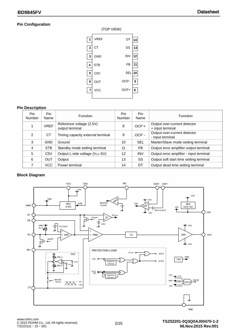
Pin Configuration
Pin Description
Block Diagram
Pin Number
Pin Name
Function Pin
Number Pin
Name Function
1 VREF Reference voltage (2.5V)
output terminal 8 OCP+
Output over-current detector
+ input terminal
2 CT Timing capacity external terminal 9 OCP- Output over-current detector
- input terminal
3 GND Ground 10 SEL Master/Slave mode setting terminal
4 STB Standby mode setting terminal 11 FB Output error amplifier output terminal
5 C5V Output L side voltage (VCC-5V) 12 INV Output error amplifier - input terminal
6 OUT Output 13 SS Output soft start time setting terminal
7 VCC Power terminal 14 DT Output dead time setting terminal
++
-ERR +
+
-
PWM LS DRV
VREF2μ A
VCC
C5V
OCP
C5V
VCC
OCP+
-
VREF
VCC
C5V
REG(2.5V)
VREF
DT
FB
SS
INV
CT
VCC
VCC
OCP+ OCP-
GND
OUT
C5V
1V±10mV
50mV±10mV
REG(VCC-5V)
DTOFF
SSOFF
TSDTSD
2V
1.5V
+
-MASTER/SLAVE
+--
200μ A
200μ A1.5V
2.0V
MASTER/SLAVE
OSC
Hold time(1.6msec)
OCP
DTLowSSOFF
DTOFF
UVLOTSD
Hold time(0.2msec)
PROTECTION LOGIC
UVLOUVLO
VCC
VREF
C5V
3.2V
2.2V
3V
+
- DTLow
1.25V
DT
STB
STB SEL
DT
SS
INV
FB
SEL
OCP-
VREF
CT
GND
STB
C5V
OUT
OCP+ VCC
1
2
3
6
5
4
7
14
13
12
11
10
9
8
(TOP VIEW)
3/25
BD9845FV
© 2015 ROHM Co., Ltd. All rights reserved. www.rohm.com
TSZ22111・15・001 06.Nov.2015 Rev.001
TSZ02201-0Q3Q0AJ00470-1-2
Absolute Maximum Ratings
Item Symbol Rating Unit
Supply Voltage VCC 36 V
Permissible Loss Pd 0.50 (Note 1) W
OUT Terminal Voltage VOUT VCC-7V to VCC V
C5V Terminal Voltage VC5V VCC-7V to VCC V
OCP Terminal Voltage VOCP VCC-7V to VCC V
Operation Temperature Range Topr -40 to +85 °C
Storage Temperature Range Tstg -55 to +150 °C
Joint Temperature Tjmax 150 °C
(Note 1) When mounted on a 70.0 mm 70.0 mm 1.6 mm glass epoxy board. Derate by 4.0 mW/C above Ta=25C. Caution: Operating the IC over the absolute maximum ratings may damage the IC. In addition, it is impossible to predict all destructive situations such as short-circuit modes, open circuit modes, etc. Therefore, it is important to consider circuit protection measures, like adding a fuse, in case the IC is operated in a special mode exceeding the absolute maximum ratings.
Recommended Operating Conditions (Ta=25C)
Item Symbol Range Unit
Supply Voltage VCC 3.6 to 35 V
Output Terminal Voltage VOUT VC5V to VCC V
Timing Capacity CCT 47 to 3000 pF
Error Amplifier Input Voltage VINV 0 to VREF-0.9 V
DT Terminal Input Voltage VDT 0 to VREF V
OCP+/- Input Voltage VOCP VCC±0.2 V
Oscillation Frequency fOSC 100 to 1500 kHz
STB Input Voltage VSTB 0 to VCC V
SEL Input Voltage VSEL 0 to VCC V
4/25
BD9845FV
© 2015 ROHM Co., Ltd. All rights reserved. www.rohm.com
TSZ22111・15・001 06.Nov.2015 Rev.001
TSZ02201-0Q3Q0AJ00470-1-2
Electrical Characteristics (Unless otherwise specified, Ta=25C, VCC=6V)
Item Symbol Standard Value
Unit Conditions Min Typ Max
[VREF Output Unit]
Output Voltage VREF 2.450 2.500 2.550 V IOUT= 0.1mA
Input Stability(Line Reg.) VLI_REG - 1 10 mV VCC= 3.6V to 35V
Load Stability(Load Reg.) VLO_REG - 2 10 mV IOUT= 0.1mA to 2mA
Current Capacity IOMAX 2 13 - mA VREF= (Typ)x0.95
[Triangular Wave Oscillator]
Oscillation Frequency fOSC 95 106 117 kHz CCP= 1800pF
Frequency Fluctuation fDV - 0 1 % VCC= 3.6V to 35V
[Soft Start Unit]
SS Source Current ISSSO 1.4 2 2.6 µA VSS= 0.5V
SS Sink Current ISSSI 5 12 - mA VSS= 0.5V
[Pause Period Adjusting Circuit]
DT Input Bias Current IDT - 0.1 1 µA VDT= 1.75V
DT Sink Current IDTSI 1 3.3 - mA VDT= 1.75V, (VOCP+)-(VOCP-)= 0.5V
[Low Input Malfunction Preventing Circuit]
Threshold Voltage VUTH 3.0 3.2 3.4 V VCC Start Detection
Hysteresis VUHYS - 0.15 0.25 V
[Error Amplifier]
Non-Inverting Input Reference Voltage VINV 0.99 1 1.01 V INV= FB
Reference Voltage Supply Fluctuation dVINV - 1 6 mV VCC= 3.6V to 35V
INV Input Bias Current IIB - 0 1 µA VINV= 1V
Open Gain AV 65 85 - dB
Max Output Voltage VFBH 2.30 - VREF V
Min Output Voltage VFBL - 0.6 1.3 V
Output Sink Current IFBSI 0.5 1.5 - mA VFB= 1.25V, VINV= 1.5V
Output Source Current IFBSO 50 105 - µA VFB= 1.25V, VINV= 0.5V
[PWM Comparator]
Input Threshold Voltage (fOSC=100kHz) Vth0 1.4 1.5 1.6 V On Duty 0%
Vth100 1.9 2 2.1 V On Duty 100%
[Output Unit]
Output ON Resistance H RONH - 4.0 10 Ω RONH= (VCC -VOUT)/ IOUT, IOUT= 0.1A
Output ON Resistance L RONL - 3.3 10 Ω RONL= (VOUT -VC5V)/ IOUT, IOUT= 0.1A
C5V Clamp Voltage VCLMP 4.5 5 5.5 V VCLMP= VCC- VC5V , VCC > 7 V
[Over-Current Protection Circuit]
Over-Current Detection Threshold Voltage
VOCPTH 0.04 0.05 0.06 V Voltage Between(OCP+) and (OCP-)
OCP-Input Bias Current IOCP- - 0.1 10 µA OCP+= VCC, OCP-= VCC-0.5V
Over-Current Detection Delay Time tDOCPTH - 200 400 ns OCP-= VCC→ VCC-0.2 V
Over-Current Detection Minimum Retention Time
tDOCPRE 0.8 1.6 - ms OCP-= VCC-0.2V→ VCC
[Standby Changeover Unit]
STB Flow-In Current ISTB - 55 100 µA VSTB= 6V
Standby Mode Setting Range VSTBL 0 - 0.5 V
Active (Master) Mode Setting Range VSTBH 3.0 - VCC V
SEL Flow-in Current ISEL - 15 30 µA VSEL= 2.5V
Master Mode Setting Range VSELL 0 - 0.5 V
Slave Mode Setting Range VSELH 2.0 - VCC V
[Device Overall]
Standby Current ICCS - 0 1 µA VSTB= 0V
Average Power Consumption ICCA 1 2.4 4 mA VINV= 0V, FB= H, VDT= 1.75V
5/25
BD9845FV
© 2015 ROHM Co., Ltd. All rights reserved. www.rohm.com
TSZ22111・15・001 06.Nov.2015 Rev.001
TSZ02201-0Q3Q0AJ00470-1-2
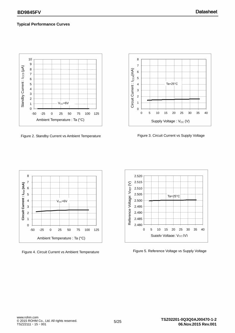
Typical Performance Curves
Figure 4. Circuit Current vs Ambient Temperature
Figure 5. Reference Voltage vs Supply Voltage
Figure 2. Standby Current vs Ambient Temperature
0
1
2
3
4 5
6
7 8
9
10
- 50
- 25
0
25
50
75
100
125
Ambient Temperature : Ta (°C)
Sta
nd
by C
urr
ent
: I C
CS
(µ
A)
VCC=6V
0
1
2
3
4
5
6
7
8
- 50
- 25
0
25
50
75
100
125
Ambient Temperature : Ta (°C)
Cir
cu
it C
urr
en
t :
I CC A
(mA
)
VCC=6V
2.480
2.485
2.490
2.495
2.500
2.505
2.510
2.515
2.520
0
5
10
15
20
25
30
35
40
Supply Voltage: VCC (V)
Refe
rence
Vo
ltag
e:
VR
EF
(V
)
Ta=25°C
0 1 2 3 4 5 6 7 8
0 5 10 15 20 25 30 35 40
Supply Voltage : VCC (V)
Circuit C
urr
ent
: I C
CA(m
A)
Ta=25°C
Figure 3. Circuit Current vs Supply Voltage
6/25
BD9845FV
© 2015 ROHM Co., Ltd. All rights reserved. www.rohm.com
TSZ22111・15・001 06.Nov.2015 Rev.001
TSZ02201-0Q3Q0AJ00470-1-2
Typical Performance Curves – continued
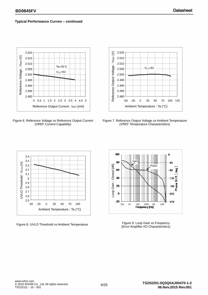
Figure 6. Reference Voltage vs Reference Output Current
(VREF Current Capability)
Figure 7. Reference Output Voltage vs Ambient Temperature
(VREF Temperature Characteristics)
Figure 8. UVLO Threshold vs Ambient Temperature
Figure 9. Loop Gain vs Frequency (Error Amplifier I/O Characteristics)
Reference Output Current : IREF (mA)
2.480
2.485
2.490
2.495
2.500
2.505
2.510
2.515
2.520
0
0.5
1
1.5
2
2.5
3
3.5
4
4.5
5
Re
fere
nce
Vo
ltag
e :
VR
EF
(V
)
Ta=25°C
VCC=6V
125
2.5
2.6
2.7
2.8 2.9 3
3.1
3.2 3.3
3.4
3.5
- 50
- 25
0
25
50
75
100
Ambient Temperature : Ta (°C)
UV
LO
Th
resh
old
: V
UT
H (V
)
2.480
2.485
2.490
2.495
2.500
2.505
2.510
2.515
2.520
- 50
- 25
0
25
50
75
100
125
Ambient Temperature : Ta (°C)
Re
fere
nce
Ou
tpu
t V
oltag
e :
VR
EF (
V)
(V)
VCC=6V
Phase
Gain
100 1K 10K 100K 1M 10M
Lo
op
Gain
: C
lose
d [d
B]
Phase
Gain
7/25
BD9845FV
© 2015 ROHM Co., Ltd. All rights reserved. www.rohm.com
TSZ22111・15・001 06.Nov.2015 Rev.001
TSZ02201-0Q3Q0AJ00470-1-2
Typical Performance Curves – continued
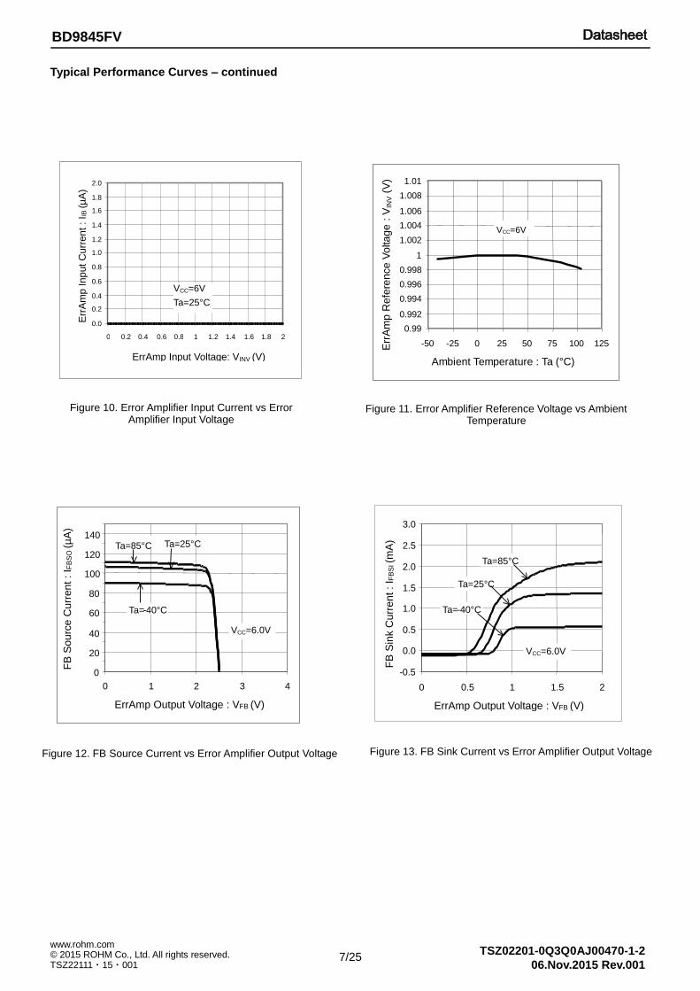
Ta=25℃
VCC=6V
Figure 10. Error Amplifier Input Current vs Error
Amplifier Input Voltage
Figure 12. FB Source Current vs Error Amplifier Output Voltage
Figure 13. FB Sink Current vs Error Amplifier Output Voltage
0
20
40
60
80
100
120
140
0
1
2
3
4
ErrAmp Output Voltage : VFB (V)
Ta=85°C
Ta=25°C
Ta= - 40°C
VCC=6.0V
0.0
0.2
0.4
0.6
0.8
1.0
1.2
1.4
1.6
1.8
2.0
0 0.2 0.4 0.6 0.8 1 1.2 1.4 1.6 1.8 2
ErrAmp Input Voltage: VINV (V)
Err
Am
p Inp
ut
Curr
en
t : I IB
(µ
A)
Ta=25°C
VCC=6V
- 0.5
0.0
0.5
1.0
1.5
2.0
2.5
3.0
0
0.5
1
1.5
2
ErrAmp Output Voltage : VFB (V)
FB
Sin
k C
urr
en
t :
I FB
SI (m
A)
VCC=6.0V
Ta=85°C
Ta=25°C
Ta= - 40°C
FB
So
urc
e C
urr
en
t :
I FB
SO
(µ
A)
0.99 0.992 0.994 0.996 0.998
1 1.002 1.004 1.006 1.008 1.01
-50 -25 0 25 50 75 100 125 Ambient Temperature : Ta (°C)
E
rrA
mp R
efe
ren
ce V
oltag
e :
VIN
V (
V)
VCC=6V
Figure 11. Error Amplifier Reference Voltage vs Ambient
Temperature
8/25
BD9845FV
© 2015 ROHM Co., Ltd. All rights reserved. www.rohm.com
TSZ22111・15・001 06.Nov.2015 Rev.001
TSZ02201-0Q3Q0AJ00470-1-2
Typical Performance Curves – continued
0 5
10 15 20 25 30 35
0 0.5 1 1.5 2 SS Voltage : VSS (V)
SS
Sin
k C
urr
en
t :
I SS
si (m
A)
VCC=6.0V
Ta=85°C
Ta=25°C Ta=-40°C
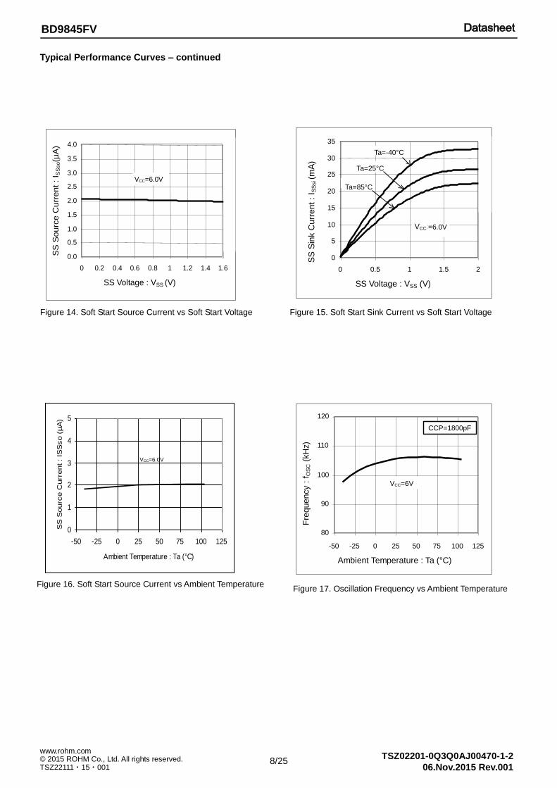
Figure 15. Soft Start Sink Current vs Soft Start Voltage
Figure 16. Soft Start Source Current vs Ambient Temperature
80
90
100
110
120
-50 -25 0 25 50 75 100 125 Ambient Temperature : Ta (°C)
Fre
que
ncy :
fO
SC (
kH
z)
VCC=6V
CCP=1800pF
Figure 17. Oscillation Frequency vs Ambient Temperature
Figure 14. Soft Start Source Current vs Soft Start Voltage
0.0 0.5 1.0 1.5 2.0 2.5 3.0 3.5 4.0
0 0.2 0.4 0.6 0.8 1 1.2 1.4 1.6 SS Voltage : VSS (V)
SS
Sou
rce C
urr
en
t :
I SS
so(µ
A)
VCC=6.0V
VCC
0
1
2
3
4
5
-50 -25 0 25 50 75 100 125
Ambient Temperature : Ta (°C)
SS
Sourc
e C
urr
ent : IS
Sso (
µA
)
VCC=6.0V
9/25
BD9845FV
© 2015 ROHM Co., Ltd. All rights reserved. www.rohm.com
TSZ22111・15・001 06.Nov.2015 Rev.001
TSZ02201-0Q3Q0AJ00470-1-2
Typical Performance Curves – continued
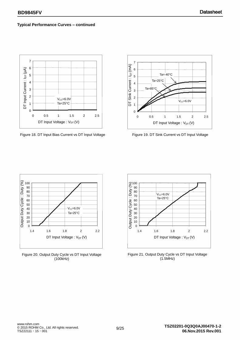
Figure 18. DT Input Bias Current vs DT Input Voltage
0 1 2 3 4 5 6 7
0 0.5 1 1.5 2 2.5 DT Input Voltage : VDT (V)
DT
SIn
k C
urr
ent
: I D
T (m
A)
Ta=85°C
Ta=25°C Ta=-40°C
VCC=6.0V
Figure 19. DT Sink Current vs DT Input Voltage
0 10 20 30 40 50 60 70 80 90
100
1.4 1.6 1.8 2 2.2 DT Input Voltage : VDT (V)
Outp
ut
Duty
Cycle
: D
uty
(%
)
VCC=6.0V Ta=25°C
Figure 20. Output Duty Cycle vs DT Input Voltage (100kHz)
0 10 20 30 40 50 60 70 80 90
100
1.4 1.6 1.8 2 2.2 DT Input Voltage : VDT (V)
Outp
ut
Duty
Cycle
: D
uty
(%
)
VCC=6.0V Ta=25°C
Figure 21. Output Duty Cycle vs DT Input Voltage (1.5MHz)
0
1
2
3
4
5
6
7
0
0.5
1
1.5
2
2.5
DT Input Voltage : VDT (V)
DT
In
pu
t C
urr
en
t :
I DT
(µ
A)
VCC=6.0V
Ta=25°C
10/25
BD9845FV
© 2015 ROHM Co., Ltd. All rights reserved. www.rohm.com
TSZ22111・15・001 06.Nov.2015 Rev.001
TSZ02201-0Q3Q0AJ00470-1-2
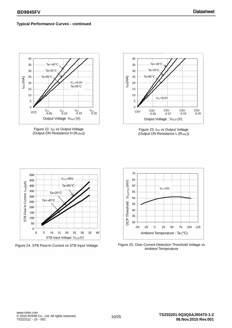
Typical Performance Curves - continued
Figure 22. IDS vs Output Voltage (Output ON Resistance H (RONH))
0 5
10 15 20 25 30 35 40
VCC -0.05 -0.10 -0.15 -0.20 Output Voltage :VOUT (V)
I DS
(m
A) Ta=85°C
Ta=25°C Ta=-40°C
VCC=6.0V
VCC VCC VCC VCC
Ta=25°C
Figure 23. IDS vs Output Voltage (Output ON Resistance L (RONL))
0 5
10 15 20 25 30 35 40
C5V -0.05 -0.10 -0.15 -0.20
Output Voltage : VOUT (V) I D
S(m
A) Ta=85°C
Ta=25°C Ta=-40°C
VCC=6.0V
C5V C5V C5V C5V
Figure 24. STB Flow-In Current vs STB Input Voltage Figure 25. Over-Current Detection Threshold Voltage vs Ambient Temperature
30 35 40 45 50 55 60 65 70
-50 -25 0 25 50 75 100 125 Ambient Temperature : Ta (°C)
OC
P T
hre
sh
old
: V
OC
PT
H (m
V)
VCC=6V
0
50
100
150
200
250
300
350
400
450
500
0 5 10 15 20 25 30 35 40
STB Input Voltage: VSTB (V)
ST
B F
low
-In C
urr
ent:
IS
TB(µ
A)
Ta=85°C
Ta=25°C
Ta=-40°C
VCC=35V
11/25
BD9845FV
© 2015 ROHM Co., Ltd. All rights reserved. www.rohm.com
TSZ22111・15・001 06.Nov.2015 Rev.001
TSZ02201-0Q3Q0AJ00470-1-2
Typical Performance Curves - continued
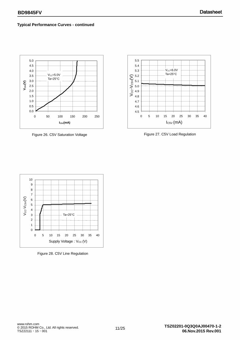
0 1 2 3 4 5 6 7 8 9
10
0 5 10 15 20 25 30 35 40 Supply Voltage : VCC (V)
VC
C-V
C5V(V
)
Ta=25°C
Figure 28. C5V Line Regulation
Figure 26. C5V Saturation Voltage
0.0 0.5 1.0 1.5 2.0 2.5 3.0 3.5 4.0 4.5 5.0
0 50 100 150 200 250 IC5V(mA)
VC
5V(V
)
VCC=5.0V Ta=25°C
Figure 27. C5V Load Regulation
4.5 4.6 4.7 4.8 4.9 5.0 5.1 5.2 5.3 5.4 5.5
0 5 10 15 20 25 30 35 40 IC5V (mA)
VC
C-V
C5
V(V
)
VCC=6.0V Ta=25°C
12/25
BD9845FV
© 2015 ROHM Co., Ltd. All rights reserved. www.rohm.com
TSZ22111・15・001 06.Nov.2015 Rev.001
TSZ02201-0Q3Q0AJ00470-1-2
10
100
1000
10000
10 100 1000 10000CT Timing Capacity (pF)
Oscill
atio
n F
requ
en
cy (
kH
z)
Ta=25℃
Application Information
1. Operation Description of Each Block and Function
(1) REG: Reference Voltage Unit The REG (2.5V) produces a voltage of 2.5V which is more stable than the supply voltage input to VCC terminal. This voltage is used as a reference voltage to the IC’s internal circuitry. This voltage is also connected to the VREF terminal. Insert a capacitor of 0.1µF to VREF terminal. The REG (VCC-5V) produces a voltage of (VCC-5V) which is used as power supply (LDO) of driver circuit (DRV). This voltage is also connected to the C5V terminal. Insert a capacitor of 1µF between VCC and C5V terminals.
(2) ERR Amp: Error Amplifier In step-down application, the inverting input, INV, of the error amplifier detects output voltage by sending back feedback current from final output stage (on load side) of switching regulator. Resistors R1 and R2 that are connected to this input terminal are used for setting the output voltage. The non-inverting input of the amplifier is connected to an internal reference voltage (1.0V). RF and CF, which are connected between FB, the output of the error amplifier, and INV, are for setting of the amplifier’s loop gain. FB is connected to the non-inverting input of PWM Comp. Setting of output voltage (VOUT) is as follows:
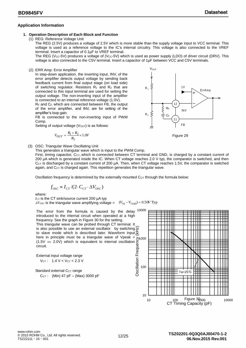
(3) OSC: Triangular Wave Oscillating Unit This generates a triangular wave which is input to the PWM Comp. First, timing capacitor, CCT, which is connected between CT terminal and GND, is charged by a constant current of 200 µA which is generated inside the IC. When CT voltage reaches 2.0 V typ, the comparator is switched, and then CCT is discharged by a constant current of 200 µA. Then, when CT voltage reaches 1.5V, the comparator is switched again, and CCT is charged again. This repetition generates the triangular wave.
Oscillation frequency is determined by the externally mounted CCT through the formula below:
where: ICT is the CT sink/source current 200 µA typ ΔVOSC is the triangular wave amplifying voltage =
The error from the formula is caused by the delay introduced to the internal circuit when operated at a high frequency. See the graph in Figure 30 for the setting. This triangular wave can be probed through CT terminal. It is also possible to use an external oscillator by switching to slave mode which is described later. Waveform input here in principle must be a triangular wave of Vpeak =
(1.5V 2.0V) which is equivalent to internal oscillation circuit.
External input voltage range
VCT : 1.4 V < VCT < 2.3 V
Standard external CCT range
CCT : (Min) 47 pF – (Max) 3000 pF
Figure 29
Figure 30
VR
RRVOUT 0.1
2
21
)2/( OSCCTCTOSC VCIf
Typ 50.0)(1000
VVV tt
V O
R 1
R 2
12
11
INV
FB
ErrAm p
R f
C f
1V
VOUT
RF CF
13/25
BD9845FV
© 2015 ROHM Co., Ltd. All rights reserved. www.rohm.com
TSZ22111・15・001 06.Nov.2015 Rev.001
TSZ02201-0Q3Q0AJ00470-1-2
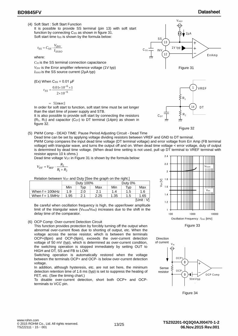
(4) Soft Start : Soft Start Function It is possible to provide SS terminal (pin 13) with soft start function by connecting CSS as shown in figure 31. Soft start time tSS is shown by the formula below:
where:
CSS is the SS terminal connection capacitance
VINV is the Error amplifier reference voltage (1V typ)
ISSSO is the SS source current (2µA typ)
(Ex) When CSS = 0.01 µF
In order for soft start to function, soft start time must be set longer than the start time of power supply and STB. It is also possible to provide soft start by connecting the resistors (R1, R2) and capacitor (CDT) to DT terminal (14pin) as shown in figure 32.
(5) PWM Comp - DEAD TIME: Pause Period Adjusting Circuit - Dead Time Dead time can be set by applying voltage dividing resistors between VREF and GND to DT terminal. PWM Comp compares the input dead time voltage (DT terminal voltage) and error voltage from Err Amp (FB terminal voltage) with triangular wave, and turns the output off and on. When dead time voltage < error voltage, duty of output is determined by dead time voltage. (When dead time setting is not used, pull up DT terminal to VREF terminal with resistor approx 10 k ohms.) Dead time voltage VDT in Figure 31 is shown by the formula below:
Relation between VDT and Duty [See the graph on the right.]
Duty 100% Duty 0%
Min Typ Max Min Typ Max
When f = 100kHz 1.9 2.0 2.1 1.4 1.5 1.6
When f = 1.5MHz 1.95 2.1 2.25 1.35 1.5 1.65
Be careful when oscillation frequency is high, the upper/lower amplitude limit of the triangular wave (Vth100/Vth0) increases due to the shift in the delay time of the comparator.
(6) OCP Comp: Over-current Detection Circuit
This function provides protection by forcibly turning off the output when abnormal over-current flows due to shorting of output, etc. When the voltage across the sense resistor, which is between the terminals OCP+(8pin) and OCP-(9pin), exceeds the over-current detection voltage of 50 mV (typ), which is determined as over-current condition, the switching operation is stopped immediately by setting OUT to HIGH and DT, SS and FB to LOW. Switching operation is automatically restored when the voltage between the terminals OCP+ and OCP- is below over-current detection voltage. In addition, although hysteresis, etc. are not set here, the minimum detection retention time of 1.6 ms (typ) is set to suppress the heating of FET, etc. (See the timing chart.) To disable over-current detection, short both OCP+ and OCP- terminals to VCC pin.
V R E F
IN V
SS
ErrAm p
2µA
C S S
1V typ
13
12
Figure 32
[Unit : V]
1
1.2
1.4
1.6
1.8
2
2.2
2.4
100 1000 10000
fOSC[KHz]
VDT[V
]
Vth100
Vth0
Figure 33
Figure 31
SSSO
INVSSSS
I
VCt
[msec] 5
102
11001.0
6
6
SSt
21
2
RR
RVV REFDT
VR EF
D T
R 1
R 2C DT
1
14
Oscillation Frequency : fOSC [kHz]
VD
T [V
]
Figure 34
Direction of current
Sense resistor
V IN
O C P +
O C P -
O C P C om p
50m Vtyp
.
8
9
14/25
BD9845FV
© 2015 ROHM Co., Ltd. All rights reserved. www.rohm.com
TSZ22111・15・001 06.Nov.2015 Rev.001
TSZ02201-0Q3Q0AJ00470-1-2
(7) STB /SEL: Standby/Master/Slave Function
Standby mode and normal mode can be switched by STB terminal (4pin).
(a) When STB<0.5V, standby mode is set.
Output stops (OUT=HIGH), REG stops and there is no circuit current (ISC = 0 µA).
(b) When STB>3.0V, normal operation mode is set.
All circuits operate. Use the controller normally in this range.
Master mode and slave mode can be switched by SEL terminal (10pin).
(a) When SEL<0.5V, master mode is set.
All circuits operate.
(b) When SEL>2.0V, slave mode is set.
Operation statusis set, but OSC block is stopped, CT terminal is High-Z here, and triangular wave is not
outputted (PWM circuit and protection circuit perform the same operation as usual.). Therefore, if the controller
is used in this mode, triangular wave is not outputted, operation is unstable, and normal output cannot be
obtained. Be careful when using the IC in this mode.
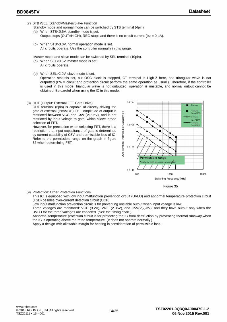
(8) OUT (Output: External FET Gate Drive) OUT terminal (6pin) is capable of directly driving the gate of external (PchMOS) FET. Amplitude of output is restricted between VCC and C5V (VCC-5V), and is not restricted by input voltage to gate, which allows broad selection of FET. However, for precaution when selecting FET, there is a restriction that input capacitance of gate is determined by current capability of C5V and permissible loss of IC. Refer to the permissible range on the graph in figure 35 when determining FET.
(9) Protection: Other Protection Functions This IC is equipped with low input malfunction prevention circuit (UVLO) and abnormal temperature protection circuit (TSD) besides over-current detection circuit (OCP). Low input malfunction prevention circuit is for preventing unstable output when input voltage is low. Three voltages are monitored: VCC (3.2V), VREF(2.35V), and C5V(VCC-3V), and they have output only when the UVLO for the three voltages are canceled. (See the timing chart.) Abnormal temperature protection circuit is for protecting the IC from destruction by preventing thermal runaway when the IC is operating above the rated temperature. (It does not operate normally.) Apply a design with allowable margin for heating in consideration of permissible loss.
Figure 35
1.E-10
1.E-09
1.E-08
1.E-07
100 1000 10000
Switching Frequency [kHz]
OU
T T
erm
inal P
erm
issib
le C
apacity [
F]
[F]
COUT_MAX
COUTMAX
(VCC=10V)
COUT_MAX
(VCC=20V) COUTMAX
(VCC=30V)
Permissible range Area below each line under each condition
15/25
BD9845FV
© 2015 ROHM Co., Ltd. All rights reserved. www.rohm.com
TSZ22111・15・001 06.Nov.2015 Rev.001
TSZ02201-0Q3Q0AJ00470-1-2
2. Timing Chart
Item Min Typ Max
Threshold Voltage (VCC) 3.0 3.2 3.4
Hysteresis - 0.15 0.25
Threshold Voltage (VREF) 2.0 2.2 2.4
Threshold Voltage (C5V) - 3.0 3.4
◎ Starting characteristics (UVLO cancel) and standby operation
UVLO Voltage [unit: V]
◎ Over-current detection (When output is shorted: Over-current detection and cancel are repeated at a specified time interval.)
SS
OCP+OCP-
Vcc
Vocpth
OCP+OCP-
DTFBCT
FB
DT
C5V
Vcc
Vcc-5V
OUT OUT
C5V
DT→"L”SS→"L”(FB→"L”)
DT(FB)、SSを開放
過電流検出過電流検出 過電流検出
検出状態を保持する最小時間
tdocpre 1.6mS
検出時の遅延時間tdocpth
Delay time in detection
Over-current detection Over-current detection Over-current detection
Minimum time retaining detection condition
tdocpre 1.6mS
Open DT (FB) and SS.
tDOCPTH
tDOCPRE
VOCPTH
VCC
VCC
VCC-5V
STB
VREF
1V
SS
DTFBCT
Vcc
Vcc-5V
OUTC5V
C5V
DT:UVLO期間中はプルダウン
FB:UVLO期間中はプルダウン
:UVLO期間中はVREFにプルアップ
OUT
②VREF>2.2VでUVLO(VREF)解除
☆UVLO(TSD)最小保持時間(0.2msec)
UVLO(Vcc,VREF)とも解除になると(Vcc-5V)Regが起動
③C5V<Vcc-3VでUVLO(C5V)解除
1.8Vtyp.
0.9Vtyp.
CTUVLO保護状態
VCC
①Vcc>3.2VでUVLO(Vcc)解除
VREF起動電圧
VREF停止電圧
■UVLOは、①Vcc②VREF③C5V全てが通常状態となった後、☆最小保持時間後に解除、①Vcc②VREF③C5VのいずれかでUVLOを検出した場合には、ただちに出力を停止。
SSは外付け容量によって設定します。図中ではイメージをつかんで頂く為同じ時間軸で表記しておりますが、実際は三角波の周期に比べ十分に長い時間を設定します。
(1) UVLO (VCC) is canceled when VCC>3.2V.
(2) UVLO (VREF) is canceled when VREF>2.2V.
VREF start voltage
VREF stop voltage
UVLO (TSD) Minimum retention time (0.2 ms)
Set SS by external capacitance.
Although SS is shown by the same time axis in the figure, in actual, set sufficiently
longer time in comparison with the cycle of triangular wave.
UVLO
When (1) VCC, (2) VREF, and (3) C5V are all in normal condition, UVLO is canceled after the minimum retention time. When UVLO is detected at any of (1) VCC, (2) VREF, and (3) C5V, output is stopped immediately. UVLO protection
condition CT: Pull-up to VREF during UVLO period
DT: Pull-down during UVLO
FB: Pull-down during UVLO
When UVLO (VCC , and VREF) is canceled, (VCC - 5V) Reg is started.
(3) UVLO (C5V) is canceled when VC5V<VCC - 3V.
VCC-5V
VCC
16/25
BD9845FV
© 2015 ROHM Co., Ltd. All rights reserved. www.rohm.com
TSZ22111・15・001 06.Nov.2015 Rev.001
TSZ02201-0Q3Q0AJ00470-1-2
O SC
+
-
+
PW M DRV
V CC
VCC-5V
+
-
+
ERR
V REF
UVLO TSD
O CP
2
V CC-5V
V CC
O CP-
+
V REF
V CC
VCC -
5V
VREFVREF
CT
INV
SS
FB
DT
VCC
V CC
STB
O CP+ O CP- G ND
O UT
C 5V
V IN
VO
(S tep-down)
5VREG
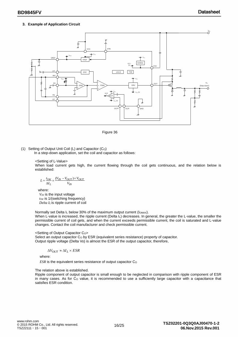
3. Example of Application Circuit
Figure 36
(1) Setting of Output Unit Coil (L) and Capacitor (CO)
In a step-down application, set the coil and capacitor as follows:
<Setting of L-Value> When load current gets high, the current flowing through the coil gets continuous, and the relation below is established:
where:
VIN is the input voltage tSW is 1/(switching frequency) Delta IL is ripple current of coil
Normally set Delta IL below 30% of the maximum output current (IOMAX). When L-value is increased, the ripple current (Delta IL) decreases. In general, the greater the L-value, the smaller the permissible current of coil gets, and when the current exceeds permissible current, the coil is saturated and L-value changes. Contact the coil manufacturer and check permissible current.
<Setting of Output Capacitor CO> Select an output capacitor CO by ESR (equivalent series resistance) property of capacitor. Output ripple voltage (Delta Vo) is almost the ESR of the output capacitor, therefore,
where:
ESR is the equivalent series resistance of output capacitor CO
The relation above is established. Ripple component of output capacitor is small enough to be neglected in comparison with ripple component of ESR in many cases. As for CO value, it is recommended to use a sufficiently large capacitor with a capacitance that satisfies ESR condition.
IN
OUTOUTIN
L
SW
V
VVV
I
tL
)(
ESRIV LOUT
17/25
BD9845FV
© 2015 ROHM Co., Ltd. All rights reserved. www.rohm.com
TSZ22111・15・001 06.Nov.2015 Rev.001
TSZ02201-0Q3Q0AJ00470-1-2
<Switching Element> Decide the switching element by using the peak current. Peak current ISW <peak> flowing through the switching element is equal to the peak current flowing through the coil, therefore the equation below is established.
Select a switching element of permissible current and having enough margin over the peak current calculated by the equation above. For Noise reduction and efficiency improvement, select a FET having an input capacitance(Ciss and Qg), On resistance as small as possible, and a Schottky diode having an inter-terminal capacitance, reverse recovery time trr and forward voltage VF as small as possible
< Input capacitor CIN >
The bypass capacitor of VCC is used by both electrolytic capacitor and ceramic capacitor. The ceramic capacitor is placed near each channel Pow-FET drain pin as possible because of supplied output switching current instantaneously from input capacitor(CIN). In case of using an electrolytic capacitor, confirm permissible ripple current.
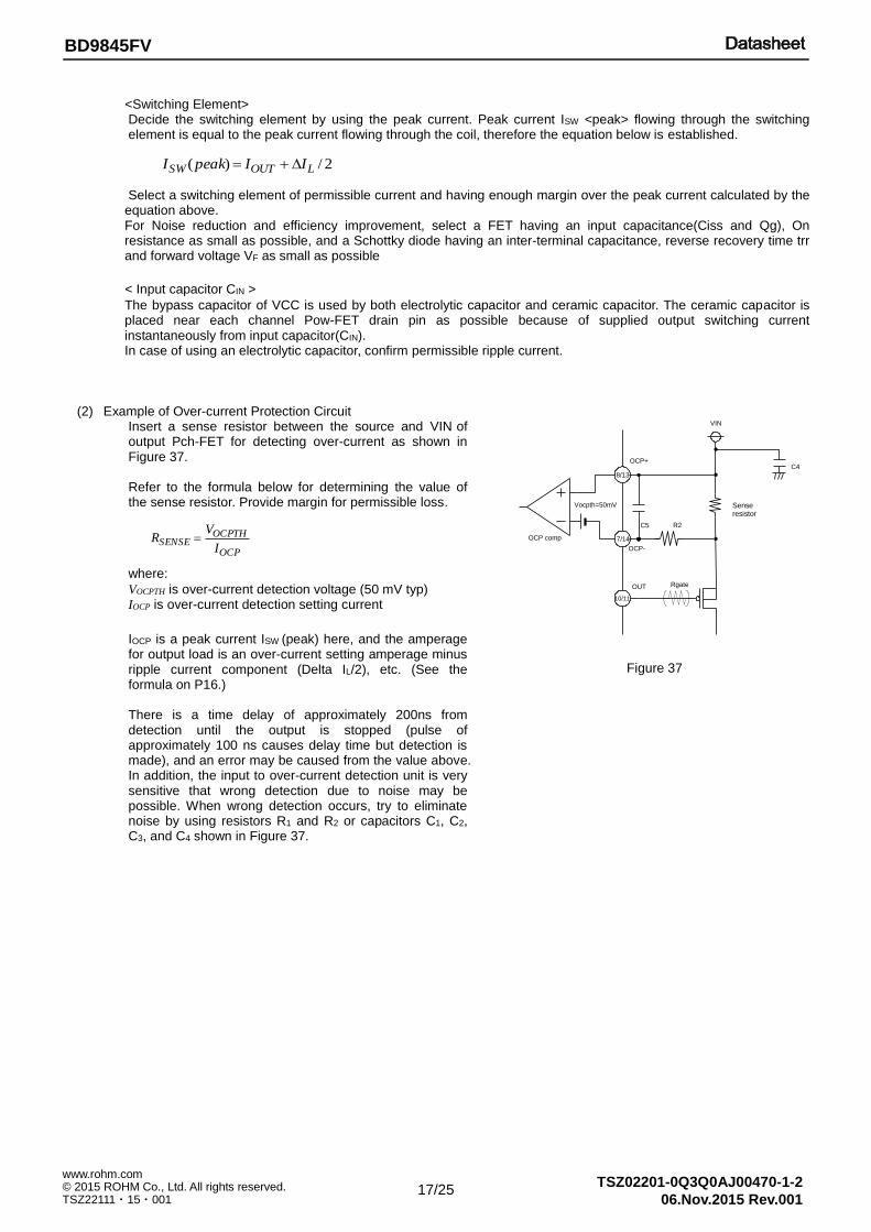
(2) Example of Over-current Protection Circuit Insert a sense resistor between the source and VIN of output Pch-FET for detecting over-current as shown in Figure 37. Refer to the formula below for determining the value of the sense resistor. Provide margin for permissible loss.
where:
VOCPTH is over-current detection voltage (50 mV typ) IOCP is over-current detection setting current
IOCP is a peak current ISW (peak) here, and the amperage for output load is an over-current setting amperage minus ripple current component (Delta IL/2), etc. (See the formula on P16.) There is a time delay of approximately 200ns from detection until the output is stopped (pulse of approximately 100 ns causes delay time but detection is made), and an error may be caused from the value above. In addition, the input to over-current detection unit is very sensitive that wrong detection due to noise may be possible. When wrong detection occurs, try to eliminate noise by using resistors R1 and R2 or capacitors C1, C2, C3, and C4 shown in Figure 37.
Figure 37
2/)( LOUTSW IIpeakI
OCP
OCPTHSENSE
I
VR
VIN
OCP+
OCP-
OUT
C5センス抵抗
OCP comp
Vocpth=50mV
8/13
7/14
10/11
C4
R2
Rgate
Sense resistor
18/25
BD9845FV
© 2015 ROHM Co., Ltd. All rights reserved. www.rohm.com
TSZ22111・15・001 06.Nov.2015 Rev.001
TSZ02201-0Q3Q0AJ00470-1-2
ton ton ton
Not enough to reduce
switching noise level Best settingToo small low pass filter
cut off freqency
OCP-voltage[after filtering]
(Dash-line [befor filtering])
Currnet Through sense
resister and FET
Low pass filter Cut off frequencyBig small
Not reaching
detection level
When FET turns on,
the switching noise add
to current wave.
Detection
level
(50mVtyp.)Detect Not detect
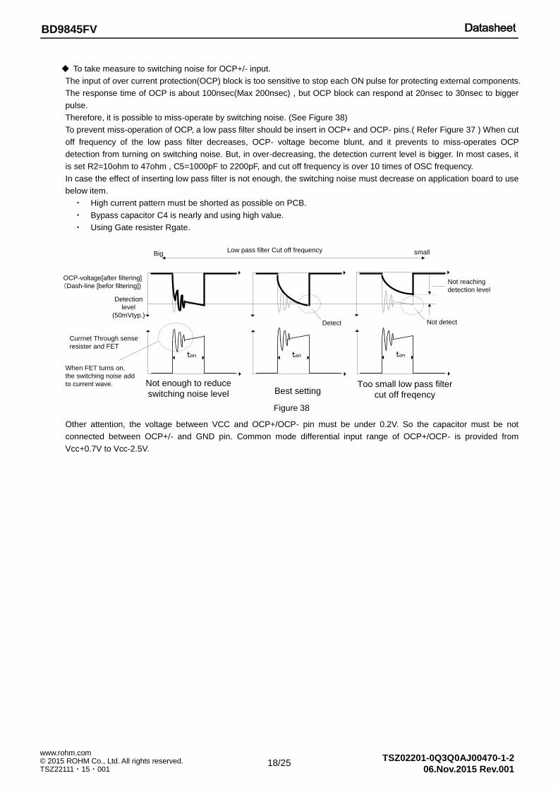
◆ To take measure to switching noise for OCP+/- input.
The input of over current protection(OCP) block is too sensitive to stop each ON pulse for protecting external components.
The response time of OCP is about 100nsec(Max 200nsec) , but OCP block can respond at 20nsec to 30nsec to bigger
pulse.
Therefore, it is possible to miss-operate by switching noise. (See Figure 38)
To prevent miss-operation of OCP, a low pass filter should be insert in OCP+ and OCP- pins.( Refer Figure 37 ) When cut
off frequency of the low pass filter decreases, OCP- voltage become blunt, and it prevents to miss-operates OCP
detection from turning on switching noise. But, in over-decreasing, the detection current level is bigger. In most cases, it
is set R2=10ohm to 47ohm , C5=1000pF to 2200pF, and cut off frequency is over 10 times of OSC frequency.
In case the effect of inserting low pass filter is not enough, the switching noise must decrease on application board to use
below item.
・ High current pattern must be shorted as possible on PCB.
・ Bypass capacitor C4 is nearly and using high value.
・ Using Gate resister Rgate.
Other attention, the voltage between VCC and OCP+/OCP- pin must be under 0.2V. So the capacitor must be not
connected between OCP+/- and GND pin. Common mode differential input range of OCP+/OCP- is provided from
Vcc+0.7V to Vcc-2.5V.
Figure 38
19/25
BD9845FV
© 2015 ROHM Co., Ltd. All rights reserved. www.rohm.com
TSZ22111・15・001 06.Nov.2015 Rev.001
TSZ02201-0Q3Q0AJ00470-1-2
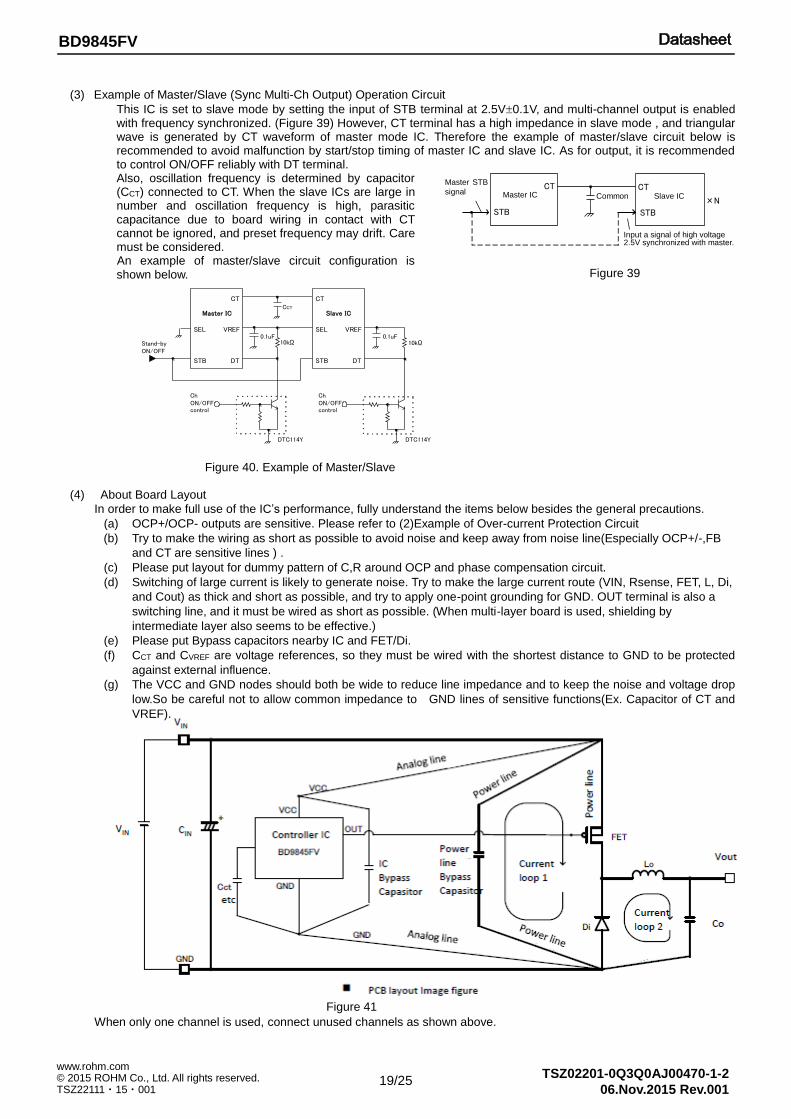
Figure 40. Example of Master/Slave
(3) Example of Master/Slave (Sync Multi-Ch Output) Operation Circuit
This IC is set to slave mode by setting the input of STB terminal at 2.5V0.1V, and multi-channel output is enabled with frequency synchronized. (Figure 39) However, CT terminal has a high impedance in slave mode , and triangular wave is generated by CT waveform of master mode IC. Therefore the example of master/slave circuit below is recommended to avoid malfunction by start/stop timing of master IC and slave IC. As for output, it is recommended to control ON/OFF reliably with DT terminal. Also, oscillation frequency is determined by capacitor (CCT) connected to CT. When the slave ICs are large in number and oscillation frequency is high, parasitic capacitance due to board wiring in contact with CT cannot be ignored, and preset frequency may drift. Care must be considered. An example of master/slave circuit configuration is shown below.
(4) About Board Layout
In order to make full use of the IC’s performance, fully understand the items below besides the general precautions.
(a) OCP+/OCP- outputs are sensitive. Please refer to (2)Example of Over-current Protection Circuit
(b) Try to make the wiring as short as possible to avoid noise and keep away from noise line(Especially OCP+/-,FB
and CT are sensitive lines ) .
(c) Please put layout for dummy pattern of C,R around OCP and phase compensation circuit.
(d) Switching of large current is likely to generate noise. Try to make the large current route (VIN, Rsense, FET, L, Di,
and Cout) as thick and short as possible, and try to apply one-point grounding for GND. OUT terminal is also a
switching line, and it must be wired as short as possible. (When multi-layer board is used, shielding by
intermediate layer also seems to be effective.)
(e) Please put Bypass capacitors nearby IC and FET/Di.
(f) CCT and CVREF are voltage references, so they must be wired with the shortest distance to GND to be protected
against external influence.
(g) The VCC and GND nodes should both be wide to reduce line impedance and to keep the noise and voltage drop
low.So be careful not to allow common impedance to GND lines of sensitive functions(Ex. Capacitor of CT and
VREF).
When only one channel is used, connect unused channels as shown above.
Figure 39
マスタと同期したHigh電圧2.5Vの信号を入力
STB
マスタIC スレブIC ×N
CT CT共通
STB
マスタSTB信号
Master STB
signal Master IC Common Slave IC
Input a signal of high voltage 2.5V synchronized with master.
SEL
STB
CT
VREF
DT
Master IC
SEL
STB
CT
VREF
DT
Slave IC
ChON/OFFcontrol
DTC114Y
CCT
0.1uF10kΩ
0.1uF10kΩ
ChON/OFFcontrol
DTC114Y
Stand-byON/OFF
Figure 41
20/25
BD9845FV
© 2015 ROHM Co., Ltd. All rights reserved. www.rohm.com
TSZ22111・15・001 06.Nov.2015 Rev.001
TSZ02201-0Q3Q0AJ00470-1-2
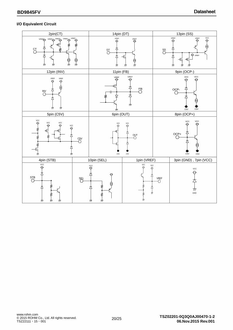
I/O Equivalent Circuit
2pin(CT) 14pin (DT) 13pin (SS)
12pin (INV) 11pin (FB) 9pin (OCP-)
5pin (C5V) 6pin (OUT) 8pin (OCP+)
4pin (STB) 10pin (SEL) 1pin (VREF) 3pin (GND) , 7pin (VCC)
INV
VREF VREF
FB
VREFVREF
OCP-
VCC
C5V C5V
VCC
OCP+
VCC
C5V
VCC
C5V
C5V
VCC
VCCVCC
VCC
OUT
VCCVCC
C5VC5V
VCC
GND
VREF
VCCVCC
SEL
VCC
CT
VREF VREF VREF VREF VREF
DT
VREF VREF
SS
VREF
VREF
VREF VCC
STB
VCC
21/25
BD9845FV
© 2015 ROHM Co., Ltd. All rights reserved. www.rohm.com
TSZ22111・15・001 06.Nov.2015 Rev.001
TSZ02201-0Q3Q0AJ00470-1-2
Operational Notes
1. Reverse Connection of Power Supply
Connecting the power supply in reverse polarity can damage the IC. Take precautions against reverse polarity when connecting the power supply, such as mounting an external diode between the power supply and the IC’s power supply pins.
2. Power Supply Lines
Design the PCB layout pattern to provide low impedance supply lines. Separate the ground and supply lines of the digital and analog blocks to prevent noise in the ground and supply lines of the digital block from affecting the analog block. Furthermore, connect a capacitor to ground at all power supply pins. Consider the effect of temperature and aging on the capacitance value when using electrolytic capacitors.
3. Ground Voltage
Ensure that no pins are at a voltage below that of the ground pin at any time, even during transient condition.
4. Ground Wiring Pattern
When using both small-signal and large-current ground traces, the two ground traces should be routed separately but connected to a single ground at the reference point of the application board to avoid fluctuations in the small-signal ground caused by large currents. Also ensure that the ground traces of external components do not cause variations on the ground voltage. The ground lines must be as short and thick as possible to reduce line impedance.
5. Thermal Consideration
Should by any chance the power dissipation rating be exceeded the rise in temperature of the chip may result in deterioration of the properties of the chip. In case of exceeding this absolute maximum rating, increase the board size and copper area to prevent exceeding the Pd rating.
6. Recommended Operating Conditions
These conditions represent a range within which the expected characteristics of the IC can be approximately obtained. The electrical characteristics are guaranteed under the conditions of each parameter.
7. Inrush Current
When power is first supplied to the IC, it is possible that the internal logic may be unstable and inrush current may flow instantaneously due to the internal powering sequence and delays, especially if the IC has more than one power supply. Therefore, give special consideration to power coupling capacitance, power wiring, width of ground wiring, and routing of connections.
8. Operation Under Strong Electromagnetic Field
Operating the IC in the presence of a strong electromagnetic field may cause the IC to malfunction.
9. Testing on Application Boards
When testing the IC on an application board, connecting a capacitor directly to a low-impedance output pin may subject the IC to stress. Always discharge capacitors completely after each process or step. The IC’s power supply should always be turned off completely before connecting or removing it from the test setup during the inspection process. To prevent damage from static discharge, ground the IC during assembly and use similar precautions during transport and storage.
10. Inter-pin Short and Mounting Errors
Ensure that the direction and position are correct when mounting the IC on the PCB. Incorrect mounting may result in damaging the IC. Avoid nearby pins being shorted to each other especially to ground, power supply and output pin. Inter-pin shorts could be due to many reasons such as metal particles, water droplets (in very humid environment) and unintentional solder bridge deposited in between pins during assembly to name a few.
22/25
BD9845FV
© 2015 ROHM Co., Ltd. All rights reserved. www.rohm.com
TSZ22111・15・001 06.Nov.2015 Rev.001
TSZ02201-0Q3Q0AJ00470-1-2
Operational Notes – continued
11. Unused Input Pins
Input pins of an IC are often connected to the gate of a MOS transistor. The gate has extremely high impedance and extremely low capacitance. If left unconnected, the electric field from the outside can easily charge it. The small charge acquired in this way is enough to produce a significant effect on the conduction through the transistor and cause unexpected operation of the IC. So unless otherwise specified, unused input pins should be connected to the power supply or ground line.
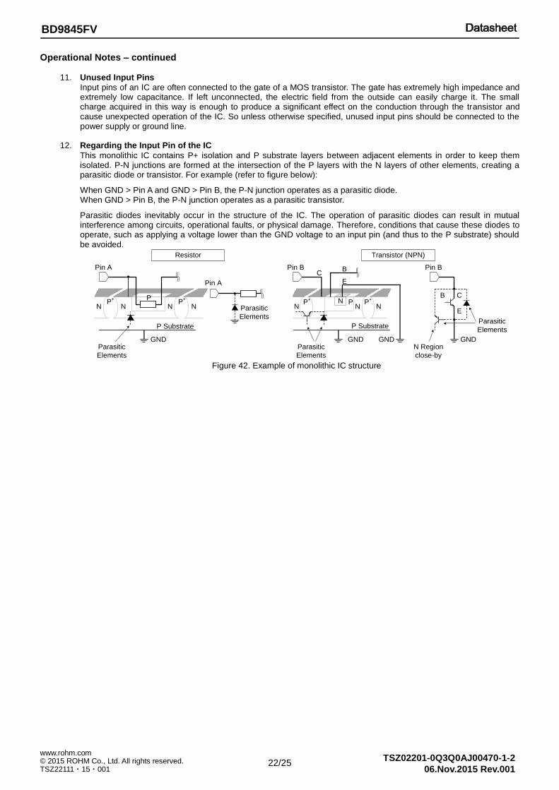
12. Regarding the Input Pin of the IC
This monolithic IC contains P+ isolation and P substrate layers between adjacent elements in order to keep them isolated. P-N junctions are formed at the intersection of the P layers with the N layers of other elements, creating a parasitic diode or transistor. For example (refer to figure below):
When GND > Pin A and GND > Pin B, the P-N junction operates as a parasitic diode. When GND > Pin B, the P-N junction operates as a parasitic transistor.
Parasitic diodes inevitably occur in the structure of the IC. The operation of parasitic diodes can result in mutual interference among circuits, operational faults, or physical damage. Therefore, conditions that cause these diodes to operate, such as applying a voltage lower than the GND voltage to an input pin (and thus to the P substrate) should be avoided.
Figure 42. Example of monolithic IC structure
N NP
+ P
N NP
+
P Substrate
GND
NP
+
N NP
+N P
P Substrate
GND GND
Parasitic
Elements
Pin A
Pin A
Pin B Pin B
B C
E
Parasitic
Elements
GNDParasitic
Elements
CB
E
Transistor (NPN)Resistor
N Region
close-by
Parasitic
Elements
23/25
BD9845FV
© 2015 ROHM Co., Ltd. All rights reserved. www.rohm.com
TSZ22111・15・001 06.Nov.2015 Rev.001
TSZ02201-0Q3Q0AJ00470-1-2
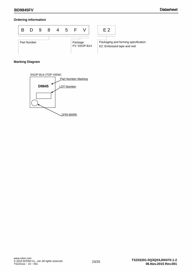
Ordering Information
B D 9 8 4 5 F V E 2
Part Number Package
FV: SSOP-B14
Packaging and forming specification
E2: Embossed tape and reel
Marking Diagram
SSOP-B14 (TOP VIEW)
D9845
Part Number Marking
LOT Number
1PIN MARK
24/25
BD9845FV
© 2015 ROHM Co., Ltd. All rights reserved. www.rohm.com
TSZ22111・15・001 06.Nov.2015 Rev.001
TSZ02201-0Q3Q0AJ00470-1-2
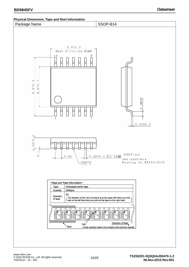
Physical Dimension, Tape and Reel information
Package Name SSOP-B14
25/25
BD9845FV
© 2015 ROHM Co., Ltd. All rights reserved. www.rohm.com
TSZ22111・15・001 06.Nov.2015 Rev.001
TSZ02201-0Q3Q0AJ00470-1-2
Revision History
Date Revision Changes
06.Nov.2015 001 New Release
DatasheetDatasheet
Notice-PGA-E Rev.002© 2015 ROHM Co., Ltd. All rights reserved.
Notice Precaution on using ROHM Products
1. Our Products are designed and manufactured for application in ordinary electronic equipments (such as AV equipment, OA equipment, telecommunication equipment, home electronic appliances, amusement equipment, etc.). If you intend to use our Products in devices requiring extremely high reliability (such as medical equipment (Note 1), transport equipment, traffic equipment, aircraft/spacecraft, nuclear power controllers, fuel controllers, car equipment including car accessories, safety devices, etc.) and whose malfunction or failure may cause loss of human life, bodily injury or serious damage to property (“Specific Applications”), please consult with the ROHM sales representative in advance. Unless otherwise agreed in writing by ROHM in advance, ROHM shall not be in any way responsible or liable for any damages, expenses or losses incurred by you or third parties arising from the use of any ROHM’s Products for Specific Applications.
(Note1) Medical Equipment Classification of the Specific Applications JAPAN USA EU CHINA
CLASSⅢ CLASSⅢ
CLASSⅡb CLASSⅢ
CLASSⅣ CLASSⅢ
2. ROHM designs and manufactures its Products subject to strict quality control system. However, semiconductor
products can fail or malfunction at a certain rate. Please be sure to implement, at your own responsibilities, adequate safety measures including but not limited to fail-safe design against the physical injury, damage to any property, which a failure or malfunction of our Products may cause. The following are examples of safety measures:
[a] Installation of protection circuits or other protective devices to improve system safety [b] Installation of redundant circuits to reduce the impact of single or multiple circuit failure
3. Our Products are designed and manufactured for use under standard conditions and not under any special or extraordinary environments or conditions, as exemplified below. Accordingly, ROHM shall not be in any way responsible or liable for any damages, expenses or losses arising from the use of any ROHM’s Products under any special or extraordinary environments or conditions. If you intend to use our Products under any special or extraordinary environments or conditions (as exemplified below), your independent verification and confirmation of product performance, reliability, etc, prior to use, must be necessary:
[a] Use of our Products in any types of liquid, including water, oils, chemicals, and organic solvents [b] Use of our Products outdoors or in places where the Products are exposed to direct sunlight or dust [c] Use of our Products in places where the Products are exposed to sea wind or corrosive gases, including Cl2,
H2S, NH3, SO2, and NO2
[d] Use of our Products in places where the Products are exposed to static electricity or electromagnetic waves [e] Use of our Products in proximity to heat-producing components, plastic cords, or other flammable items [f] Sealing or coating our Products with resin or other coating materials [g] Use of our Products without cleaning residue of flux (even if you use no-clean type fluxes, cleaning residue of
flux is recommended); or Washing our Products by using water or water-soluble cleaning agents for cleaning residue after soldering
[h] Use of the Products in places subject to dew condensation
4. The Products are not subject to radiation-proof design. 5. Please verify and confirm characteristics of the final or mounted products in using the Products. 6. In particular, if a transient load (a large amount of load applied in a short period of time, such as pulse. is applied,
confirmation of performance characteristics after on-board mounting is strongly recommended. Avoid applying power exceeding normal rated power; exceeding the power rating under steady-state loading condition may negatively affect product performance and reliability.
7. De-rate Power Dissipation depending on ambient temperature. When used in sealed area, confirm that it is the use in
the range that does not exceed the maximum junction temperature. 8. Confirm that operation temperature is within the specified range described in the product specification. 9. ROHM shall not be in any way responsible or liable for failure induced under deviant condition from what is defined in
this document.
Precaution for Mounting / Circuit board design 1. When a highly active halogenous (chlorine, bromine, etc.) flux is used, the residue of flux may negatively affect product
performance and reliability.
2. In principle, the reflow soldering method must be used on a surface-mount products, the flow soldering method must be used on a through hole mount products. If the flow soldering method is preferred on a surface-mount products, please consult with the ROHM representative in advance.
For details, please refer to ROHM Mounting specification

DatasheetDatasheet
Notice-PGA-E Rev.002© 2015 ROHM Co., Ltd. All rights reserved.
Precautions Regarding Application Examples and External Circuits 1. If change is made to the constant of an external circuit, please allow a sufficient margin considering variations of the
characteristics of the Products and external components, including transient characteristics, as well as static characteristics.
2. You agree that application notes, reference designs, and associated data and information contained in this document
are presented only as guidance for Products use. Therefore, in case you use such information, you are solely responsible for it and you must exercise your own independent verification and judgment in the use of such information contained in this document. ROHM shall not be in any way responsible or liable for any damages, expenses or losses incurred by you or third parties arising from the use of such information.
Precaution for Electrostatic
This Product is electrostatic sensitive product, which may be damaged due to electrostatic discharge. Please take proper caution in your manufacturing process and storage so that voltage exceeding the Products maximum rating will not be applied to Products. Please take special care under dry condition (e.g. Grounding of human body / equipment / solder iron, isolation from charged objects, setting of Ionizer, friction prevention and temperature / humidity control).
Precaution for Storage / Transportation 1. Product performance and soldered connections may deteriorate if the Products are stored in the places where:
[a] the Products are exposed to sea winds or corrosive gases, including Cl2, H2S, NH3, SO2, and NO2 [b] the temperature or humidity exceeds those recommended by ROHM [c] the Products are exposed to direct sunshine or condensation [d] the Products are exposed to high Electrostatic
2. Even under ROHM recommended storage condition, solderability of products out of recommended storage time period may be degraded. It is strongly recommended to confirm solderability before using Products of which storage time is exceeding the recommended storage time period.
3. Store / transport cartons in the correct direction, which is indicated on a carton with a symbol. Otherwise bent leads
may occur due to excessive stress applied when dropping of a carton. 4. Use Products within the specified time after opening a humidity barrier bag. Baking is required before using Products of
which storage time is exceeding the recommended storage time period.
Precaution for Product Label QR code printed on ROHM Products label is for ROHM’s internal use only.
Precaution for Disposition When disposing Products please dispose them properly using an authorized industry waste company.
Precaution for Foreign Exchange and Foreign Trade act Since concerned goods might be fallen under listed items of export control prescribed by Foreign exchange and Foreign trade act, please consult with ROHM in case of export.
Precaution Regarding Intellectual Property Rights 1. All information and data including but not limited to application example contained in this document is for reference
only. ROHM does not warrant that foregoing information or data will not infringe any intellectual property rights or any other rights of any third party regarding such information or data.
2. ROHM shall not have any obligations where the claims, actions or demands arising from the combination of the Products with other articles such as components, circuits, systems or external equipment (including software).
3. No license, expressly or implied, is granted hereby under any intellectual property rights or other rights of ROHM or any third parties with respect to the Products or the information contained in this document. Provided, however, that ROHM will not assert its intellectual property rights or other rights against you or your customers to the extent necessary to manufacture or sell products containing the Products, subject to the terms and conditions herein.
Other Precaution 1. This document may not be reprinted or reproduced, in whole or in part, without prior written consent of ROHM.
2. The Products may not be disassembled, converted, modified, reproduced or otherwise changed without prior written consent of ROHM.
3. In no event shall you use in any way whatsoever the Products and the related technical information contained in the Products or this document for any military purposes, including but not limited to, the development of mass-destruction weapons.
4. The proper names of companies or products described in this document are trademarks or registered trademarks of ROHM, its affiliated companies or third parties.
DatasheetDatasheet
Notice – WE Rev.001© 2015 ROHM Co., Ltd. All rights reserved.
General Precaution 1. Before you use our Pro ducts, you are requested to care fully read this document and fully understand its contents.
ROHM shall n ot be in an y way responsible or liabl e for fa ilure, malfunction or acci dent arising from the use of a ny ROHM’s Products against warning, caution or note contained in this document.
2. All information contained in this docume nt is current as of the issuing date and subj ect to change without any prior
notice. Before purchasing or using ROHM’s Products, please confirm the la test information with a ROHM sale s representative.
3. The information contained in this doc ument is provi ded on an “as is” basis and ROHM does not warrant that all
information contained in this document is accurate an d/or error-free. ROHM shall not be in an y way responsible or liable for any damages, expenses or losses incurred by you or third parties resulting from inaccuracy or errors of or concerning such information.