wafer cleaning and etching in high efficiency n- type...
TRANSCRIPT

Wafer cleaning and etching in high efficiency n-
type solar cell processing
Dr. Florian Buchholz
[email protected]; +49 7531 36 183 553

Florian Buchholz, June 9th 2017
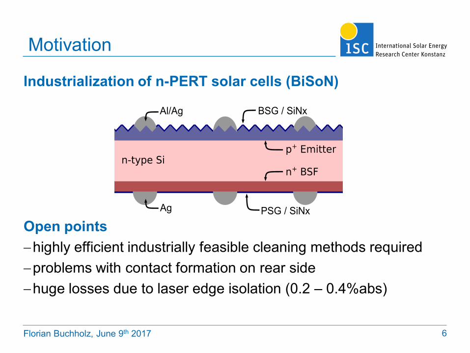
Motivation
2
From lab to fab: n-PERT solar cells (BiSoN)
Advantages:
high bificaility (>90%), eta potential > 21%, no degradation
Only standard equipment required (wet etching, P / B tube
diffusion (low pressure), PECVD, screen priting)

Florian Buchholz, June 9th 2017
Motivation
3
From lab to fab: n-PERT solar cells (BiSoN)
Industrial feasible cleaning before diffusion:
Lab standard (POR):
Not feasible

Florian Buchholz, June 9th 2017
Motivation
4
Industrialization of n-PERT solar cells (BiSoN)
Issues with rear side contact formation, increasing likelyhood

Florian Buchholz, June 9th 2017
Motivation
5
Industrialization of n-PERT solar cells (BiSoN)
Laser edge isolation causes 0.2 – 0.4%abs efficiency losses
Florian Buchholz, June 9th 2017
Motivation
6
Industrialization of n-PERT solar cells (BiSoN)
Open points
highly efficient industrially feasible cleaning methods required
problems with contact formation on rear side
huge losses due to laser edge isolation (0.2 – 0.4%abs)

Florian Buchholz, June 9th 2017
Content
7
Cleaning before diffusions
Alkaline polishing of diamond wire sawed wafers
Wet chemical edge isolation
Summary and conclusion

Florian Buchholz, June 9th 2017 8
Cleaning before diffusions
Alkaline polishing of diamond wire sawed wafers
Wet chemical edge isolation
Summary and conclusion

Florian Buchholz, June 9th 2017
Model system for cleaning optimization
Thermal oxidation more sensitive than actual production
process
Cleaning before diffusion
9
Boron diffusion of n-type wafers
cleaning after texturing cleaning after texturing
Thermal oxidation of p-type wafers

Florian Buchholz, June 9th 2017
Ozone based cleaning known from semiconductor fabrication
Cleaning before diffusion
10
Pretest x=
H2O
HCl (0.1%)
HCl/HF (0.1%/0.05%)
HF (0.05%)
HCl/HF dip only

Florian Buchholz, June 9th 2017
Results pre-test on KOH/IPA textured wafers
Cleaning before diffusion
Simple HF-base system chosen for further testing

Florian Buchholz, June 9th 2017
Optimization for different surfaces
Design of Experiment (DoE)
Diamond and slurry sawed wafers
(of different suppliers)
saw damage etching and texturing (RENA monoTEX)
Concentration range: 0.01 – 1%
Immersion time 2 – 10 min
Cleaning before diffusion
12

Florian Buchholz, June 9th 2017
Modelling outcome
Cleaning after SDE (wafers from different suppliers were used)
Cleaning before diffusion
13
Optimum: c(HF) = 0.02 – 0.035%, longer times slightly favored

Florian Buchholz, June 9th 2017
Modelling outcome
Cleaning after texturing (RENA monoTEX)
Cleaning before diffusion
14
Optimum: c(HF) = 0.04 – 0.1%, longer times clearly favored
Florian Buchholz, June 9th 2017
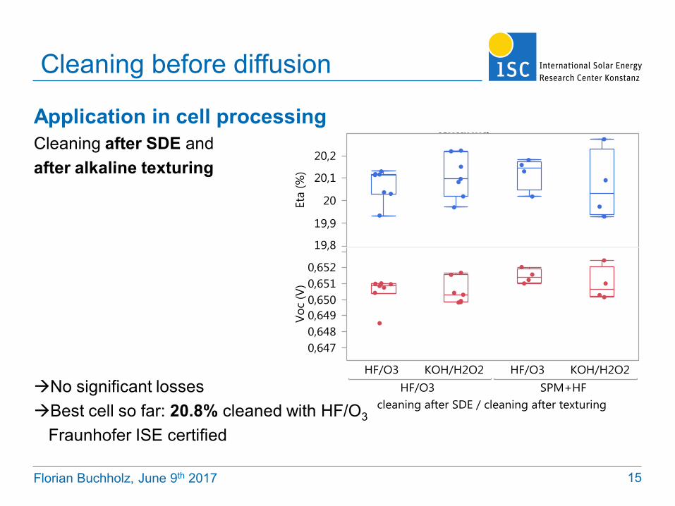
Application in cell processing
Cleaning after SDE and
after alkaline texturing
No significant losses
Best cell so far: 20.8% cleaned with HF/O3
Fraunhofer ISE certified
Cleaning before diffusion
15

Florian Buchholz, June 9th 2017 16
Cleaning before diffusions
Alkaline polishing of diamond wire sawed wafers
Wet chemical edge isolation
Summary and conclusion

Florian Buchholz, June 9th 2017
Problem: Contact formation on rear side fails
Rear side surface too flat? Doping profile variation?
Varied in the experiment:
Wafer supplier
Alkaline polishing (SDE) etching depth: 3 – 10 µm
45 and 82 Ohm/sq diffusion
Alkaline polishing of diamond wire
sawed wafers
17

Florian Buchholz, June 9th 2017
FF
Alkaline polishing of diamond wire
sawed wafers
18

Florian Buchholz, June 9th 2017
Eta
Alkaline polishing of diamond wire
sawed wafers
19

Florian Buchholz, June 9th 2017
Surface roughness measurement
Alkaline polishing of diamond wire
sawed wafers
20
State-of-the-art material only requires 3 µm saw damage removal
For high sheet resistance diffusion FF heavily relates to surface roughness

Florian Buchholz, June 9th 2017 21
Alkaline polishing of diamond wire sawed wafers
Cleaning before diffusions
Wet chemical edge isolation
Summary and conclusion

Florian Buchholz, June 9th 2017
Optimized edge isolation for (n-)PERT cells
using standard equipment
slightly modified process
Alkaline polishing of diamond wire
sawed wafers
22

Florian Buchholz, June 9th 2017
Optimized edge isolation for (n-)PERT cells
Alkaline polishing of diamond wire
sawed wafers
23
no more losses due to edge isolation
overall gain in eta has been observed

Florian Buchholz, June 9th 2017 24
Alkaline polishing of diamond wire sawed wafers
Cleaning before diffusions
Wet chemical edge isolation
Summary and conclusion
Florian Buchholz, June 9th 2017
Content
25
Open points
highly efficient industrially feasible cleaning methods required
problems with contact formation on rear side
huge losses due to laser edge isolation
Solved:
low concentration HF/O3 has been optimized and tested
low rear side etching and lower sheet resistance on BS
wet edge isolation has been developed
Process transfer will start in Q4 2017

Thank you for your attention
and special thanks to the ISC Konstanz BiSoN team.
Dr. Florian Buchholz
[email protected]; +49 7531 36 183 553