wavelink low bandwidth differential probes operator's manual
TRANSCRIPT

Operator’s Manual WaveLink Low-Bandwidth (4, 6 GHz) Differential Probe


WaveLink Low-Bandwidth Differential Probe (4, 6 GHz)
Operator's Manual October, 2016

WaveLink Low-Bandwidth Differential Probe (4, 6 GHz) Operator's Manual
© 2016 Teledyne LeCroy. All rights reserved.
Unauthorized duplication of Teledyne LeCroy documentation materials other than for internal sales and distribution purposes is strictly prohibited. However, clients are encouraged to distribute and duplicate Teledyne LeCroy documentation for their own internal educational purposes.
Teledyne LeCroy and other product or brand names are trademarks or requested trademarks of their respective holders. Information in this publication supersedes all earlier versions. Specifications are subject to change without notice.
927688-00 Rev A October, 2016

Operator’s Manual
i
Contents Safety Instructions ..................................................................................................................... 1
Symbols .......................................................................................................................................... 1 Precautions ..................................................................................................................................... 1 Operating Environment .................................................................................................................. 2
Introduction ................................................................................................................................ 3 Wide Variety of Tip and Leads ....................................................................................................... 3 Exceptional Waveform Fidelity ...................................................................................................... 3 Unique QuickLink Architecture ...................................................................................................... 3
Modular Probe Components ....................................................................................................... 4 Platform Cable Assembly .............................................................................................................. 7 Amplifier Module ............................................................................................................................ 9 Positioner Tip (Browser) Kit ........................................................................................................ 10 Complete Probe System .............................................................................................................. 10 Optional Accessories ................................................................................................................... 11
Probe Operation ....................................................................................................................... 13 Interchangeability and Calibration .............................................................................................. 13 Handling the Probe ....................................................................................................................... 14 Connecting an Amplifier Module to a Platform/Cable Assembly ............................................. 14 Connecting Interconnect Leads/Tips to the Amplifier .............................................................. 15 Connecting the Probe to an Oscilloscope .................................................................................. 17 Connecting the Probe to the Test Circuit ................................................................................... 17 Using Positioning Tools ............................................................................................................... 26 Controlling the Probe from the Oscilloscope ............................................................................. 33 Deskewing ..................................................................................................................................... 36
Maintenance............................................................................................................................. 41 Cleaning ........................................................................................................................................ 41 Replacing Damping Resistors on the SI Lead ............................................................................ 41 Replacing Tips and Sockets on the Positioner Tip .................................................................... 43 Returning a Product for Service .................................................................................................. 45

WaveLink Low Bandwidth (4, 6 GHz) Differential Probe
ii
Service Options .............................................................................................................................46 Consumables and Replacement Parts ........................................................................................48
Performance Verification .......................................................................................................... 55 Functional Test .............................................................................................................................56 Performance Verification Test .....................................................................................................60
Reference Material ................................................................................................................... 67 Technical Support .........................................................................................................................67 Specifications ................................................................................................................................67 Certifications .................................................................................................................................68 Warranty .........................................................................................................................................70 Probe Input Loading ......................................................................................................................70 Offset ..............................................................................................................................................80 Dynamic Range .............................................................................................................................81 Differential Mode and Common Mode ........................................................................................81 Differential Mode Range and Common Mode Range .................................................................82 Common Mode Rejection Ratio ...................................................................................................83
Operator’s Manual
1
Safety Instructions To maintain the probe in a correct and safe condition, observe generally accepted safety procedures in addition to the precautions specified in this section. The overall safety of any system incorporating this product is the responsibility of the assembler of the system.
Symbols These symbols appear on the probe and accessories or in this manual to alert you to important safety considerations.
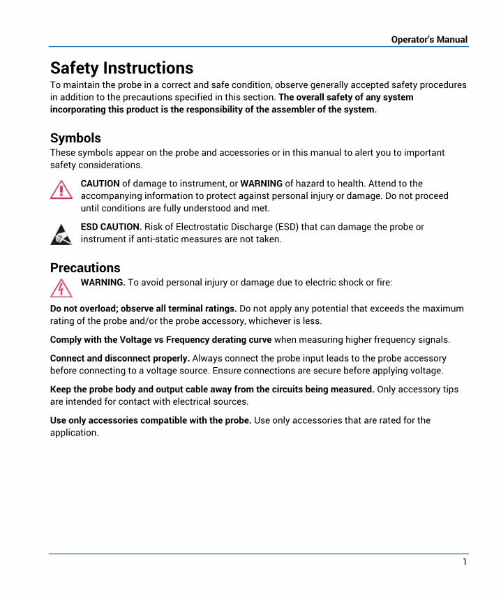
CAUTION of damage to instrument, or WARNING of hazard to health. Attend to the accompanying information to protect against personal injury or damage. Do not proceed until conditions are fully understood and met.
ESD CAUTION. Risk of Electrostatic Discharge (ESD) that can damage the probe or instrument if anti-static measures are not taken.
Precautions WARNING. To avoid personal injury or damage due to electric shock or fire:
Do not overload; observe all terminal ratings. Do not apply any potential that exceeds the maximum rating of the probe and/or the probe accessory, whichever is less.
Comply with the Voltage vs Frequency derating curve when measuring higher frequency signals.
Connect and disconnect properly. Always connect the probe input leads to the probe accessory before connecting to a voltage source. Ensure connections are secure before applying voltage.
Keep the probe body and output cable away from the circuits being measured. Only accessory tips are intended for contact with electrical sources.
Use only accessories compatible with the probe. Use only accessories that are rated for the application.

WaveLink Low Bandwidth (4, 6 GHz) Differential Probe
2
CAUTION. To avoid damaging the equipment:
Use only as specified. The probe is intended to be used only with compatible Teledyne LeCroy instruments. Use of the probe and/or the equipment it is connected to in a manner other than specified may impair the protection mechanisms.
Do not bend cables excessively.
Use only within the operational environment listed. Do not use in wet or explosive atmospheres.
Keep product surfaces clean and dry.
Do not operate with suspected failures. Before each use, inspect the probe and accessories for any damage such as tears or other defects in the probe body, cable jacket, accessories, etc. If any part is damaged, cease operation immediately and sequester the probe from inadvertent use.
Operating Environment The accessory is intended for indoor use and should be operated in a clean, dry environment. Before using this product, ensure that its operating environment is maintained within these parameters:
Temperature: 5° to 40° C.
Humidity: Maximum relative humidity 90 % for temperatures up to 31° C decreasing linearly to 50 % relative humidity at 40° C.
Altitude: Up to 10,000 ft (3,048 m).

Operator’s Manual
3
Introduction Teledyne LeCroy’s WaveLink 4-6 GHz Differential Probes are a general purpose probing solution with high-input dynamic range and offset range capability. The range of capabilities is ideal for a variety of high-speed DDR signals where high dynamic range and large offset requirements are common.
Wide Variety of Tip and Leads The wide variety of tips offered with the Dx10/Dx20 provides confidence that the most challenging test points can be probed. With seven different tips available, the Dx10/Dx20 provides great flexibility when probing, while maintaining signal integrity. An assortment of hands-free probe holders eases the challenge of connecting multiple leads to a board.
Exceptional Waveform Fidelity WaveLink probes provide superior loading characteristics and are calibrated with a custom “fine- tuned” frequency response. The ultra-low loading coupled with a flat frequency response ensure accurate measurements.
Unique QuickLink Architecture The unique QuickLink architecture allows for probe tips to be quickly attached to or removed from a WaveLink differential amplifier. Unlike other “consumable” probe tip solutions which rely on tiny, delicate tips located very close to the Device Under Test (DUT), the QuickLink Solder-In tip has an integral 9-inch lead. QuickLink Solder-In tips are low cost, making it easy to equip multiple test points and DUTs while eliminating time-consuming resoldering of connectors.
NOTE: The Certificate of Calibration shipped with each probe indicates that the system meets the specifications when using the components listed in the Certificate. Download the latest version of X-Stream™ software to run your WaveLink probe with maximum performance.
ESD Sensitive: The tips of the WaveLink probes are sensitive to Electrostatic Discharge (ESD). Avoid causing damage to the probe by always following anti-static procedures when using or handling the probe.

WaveLink Low Bandwidth (4, 6 GHz) Differential Probe
4
Modular Probe Components Wires attached to probe tips/leads add inductance or capacitance to the input, causing various effects that degrade the performance of the probe and result in reduced bandwidth, changes in loading impedance, and ultimately incorrect presentation of the signal.
The WaveLink modular design consists of a platform/cable assembly, differential amplifier module supplied with interconnect leads, and positioner tip (browser), which may be purchased separately or together as a complete probe system (-PS). Other optional leads and accessories are available to complement this core system. The variety of interchangeable leads eliminates the need for external wires or other accessories in the high-impedance path of the input signal, assuring proper transmission of the signal as it passes through the probe.
WaveLink 4, 6 GHz Probe Family

Operator’s Manual
5
You may order nearly any combination of platform/cable assembly and amplifier module, depending on your oscilloscope and requirements. At time of shipment, Teledyne LeCroy serializes the individual components and calibrates them as a system. To achieve maximum performance and warranted specifications, the calibrated components should be used together, as serialized. If additional components are purchased, you may return the serialized system to Teledyne LeCroy for re-calibration to ensure performance.
NOTE: Bandwidth is limited by the lowest bandwidth component. The typical use case is to purchase a single platform/cable assembly that matches the amplifier bandwidth rating. System calibration is required for all interconnected components to guarantee system performance.
Accessories Table
WL-PBUS-CASE WL-PLINK-CASE
Dx10-A Dx20-A
Dx10PT-KIT Dx20PT-KIT
Dx10-A-PS Dx20-A-PS Dx00A-AT Dx10-SI-HiTemp
Dx20-SI-HiTemp Dx10-QL-3SI Dx20-QL-3SI
Platform/Cable Assembly
Platform/Cable Assembly 1 each - - 1 each - - -
Freehand Probe Holder 1 each - - 1 each - - -
Probe Deskew Fixture 1 each - - 1 each - - -
Platform/Cable Assembly Mounting Clip
1 each - - 1 each 1 each 1 each -
Probe Cable Clamp 2 each - - 2 each 1 each 1 each -
Deluxe Soft Carrying Case 1 each - - 1 each - - -
Foam Insert for Carrying Case
1 each - - 1 each - - -
Protective Storage Case 1 each - - 1 each - - -
Plastic Tray for Storage Case 1 each - - 1 each - - -
Amplifier Module
Amplifier Module - 1 each - 1 each - - -
Solder-in Lead Set - 1 each - 1 each - - -
Spare Damping Resistors for SI Tip
- 1 set 5 - 1 set 5 - - -
Tip Retaining Clip - 1 each - 1 each - - -
Adhesive Tape - 1 set - 1 set - - -
Quick Connect Lead Set - 1 each - 1 each - - -

WaveLink Low Bandwidth (4, 6 GHz) Differential Probe
6
WL-PBUS-CASE WL-PLINK-CASE
Dx10-A Dx20-A
Dx10PT-KIT Dx20PT-KIT
Dx10-A-PS Dx20-A-PS Dx00A-AT Dx10-SI-HiTemp
Dx20-SI-HiTemp Dx10-QL-3SI Dx20-QL-3SI
Damping Resistors for QC Tip
- 2 sets 10 2 sets 10 - - -
Square Pin Lead Set - 1 each - 1 each - - -
Ground Lead - 1 each - 1 each - - -
Ground Clip - 1 each - 1 each - - -
Operator’s Manual - 1 each - 1 each 1 each - -
Accessory Info Sheet - 1 each - 1 each - - -
Positioner Tip Kit - - - - -
Positioner Tip (Browser) - - 1 each 1 each - - -
Replacement Pogo Pins for Dx10-PT/Dx20-PT
- - 1 set 1 set - - -
Positioner Tip Probe Guides - - 1 each 1 each - - -
XYZ Positioner - - 1 each 1 each - - -
Adhesive Tape for XYZ Positioner
- - 1 set 1 set - - -
Browser Wand for PT Tip - - 1 each 1 each - - -
Interlock Pieces for PT Tip - - 1 each 1 each - - -
Swivel for PT Tip - - 1 each 1 each - -
Adjustable Tip Module
Adjustable Tip Module - - - - 1 each - -
Protective Cover for AT Module
- - - - 1 each - -
HiTemp Lead Set
HiTemp SI Lead - - - - - 1 each -
HiTemp Cable - - - - - 1 each -
QuickLink Lead Set
QuickLink Adapter - - - - - - 1 each
QL-SI Tips 3 each

Operator’s Manual
7
Platform Cable Assembly The platform/cable assembly forms the foundation of the probe, attaching the probe amplifier to the oscilloscope. It is supplied in two different configurations:
• WL-PLINK for use with ProLink interface (≥4 GHz)
• WL-PBUS for use with ProBus interface
NOTE: WL-PLINK-A is compatible with D610-A/620-A and D410-A/420-A.
Platform Cable Assembly provided with WL-PLINK-CASE
Platform Cable Assembly provided with WL-PBUS-CASE
The platform/cable assembly is delivered with a variety of accessories in a deluxe, soft carrying case.

WaveLink Low Bandwidth (4, 6 GHz) Differential Probe
8
The platform/cable assembly:
• Provides power to the probe amplifier from the oscilloscope.
• Communicates to the oscilloscope the identifying characteristics of the amplifier that is connected to the probe so that the oscilloscope channel can be set to the correct probe attenuation value automatically (software prompts you to identify the tip used).
• Transmits the amplifier output along a well-defined low loss transmission line into the oscilloscope input, and terminates the probe appropriately at that point.
WL-PLINK-CASE
NOTE: Throughout the manual, the terms WL-PLINK-CASE or WL-PBUS-CASE is used when referring to the complete orderable kit that includes the deluxe soft carrying case and accessories. The abbreviated terms WL-PLINK or WL-PBUS is used when referring to the physical assembly.

Operator’s Manual
9
Amplifier Module The amplifier modules contain the active, differential amplifier circuitry. A selection of interconnect leads/tips with different electrical and physical characteristics allow you to choose the tip appropriate for the application. Amplifier models D610-A, D620-A, D410-A, and D420-A connect to any WL-PLINK or WL-PBUS platform/cable assembly.
NOTE: While the D6x0-A amplifier modules can be used with a WL-PBUS platform/cable assembly, this combination would not deliver full system bandwidth with 4 or 6 GHz oscilloscopes.
Interconnect Leads/Tips One each of these leads are delivered standard with each amplifier module. See Interchangeability and Calibration on page 13.
SOLDER-IN LEAD The Solder-In (SI) lead provides the highest possible performance in stationery installations. The design of the SI lead minimizes circuit AC loading by providing high probe AC loading over a wide frequency range. The SI lead is supplied with:
• Two small, pre-installed and pre-trimmed attenuating (damping) resistors connected to the flexible transmission line. The resistors are soldered directly into the connection points of the circuit under test, providing a reliable, intermittence-free connection.
• Five replacement damping resistors.
The pre-installed resistor design eliminates the need to custom cut and solder lengths of wire to the end of the lead and to the DUT. Damping resistors may be easily replaced in the field to provide maximum serviceability over the life of the SI lead.
The very small and precisely cut resistors have the advantage of locating the damping resistance of the probe tip as close to the DUT as possible, thereby eliminating the need for long lengths of wire which can impact loading and frequency response. The two resistors may be spaced as desired to connect to a wide variety of circuits.
SQUARE PIN LEAD The Square Pin (SP) lead can be used on boards where standard 0.025” square pins are used for interconnect. The highly flexible, 145 mm (5.7”) long Square Pin lead connects directly with a pair of square pins mounted on standard 0.100” (2.54 mm) centers.
Because of the parasitic inductance of the square pins, the probe will not support maximum bandwidth or minimum rise time when used with an oscilloscope with greater than 3 GHz bandwidth. The added inductance of the square pins limits the measurements to signals of 3 GHz or lower bandwidth.

WaveLink Low Bandwidth (4, 6 GHz) Differential Probe
10
QUICK CONNECT LEAD The Quick Connect (QC) lead allows the probe to be moved quickly between different test points of the circuit. A pair of small damping resistors (supplied with the probe) is soldered to the circuit’s test points, while the ends of the damping resistors plug into the small connector at the probe tip for a reliable, quick connection. Two sets of 10 resistors are shipped with the probe. This lead set is limited to 4 GHz bandwidth.
Ground Lead and Clip The Ground Lead (PACC-LD005) and the Ground Clip (PK006-4) are provided with each amplifier module and can be used to connect to ground of the circuit under test. While the ground lead is not required for high-frequency measurements, it can help to ground floating test circuits to keep the common mode within the maximum specified range.
Positioner Tip (Browser) Kit The Positioner Tip (PT) provides the ability to access the signal on the DUT without permanently attaching a lead or other device. It combines high performance with quick access to a variety of probe points when used as a hand-held browser (with the wand attachment). When used with a positioner tool, it is a fast and convenient method to re-position a fixed test point.
The pogo pin tips are adjustable from 0 to 3.5 mm (0 to 0.14") and have 0.6 mm of Z-Axis compliance. Because of its thin form factor and spring-loaded tips, the positioner tip is ideally suited for use with multiple probes in tight areas such as the back side of boards with ball-grid array packaged ICs.
Two replacement resistive tips are provided with the positioner tip. These tips may be replaced in the field if damaged.
Complete Probe System By design, the WaveLink probes are modular in nature. However, to make selection easy, a complete probe system (-PS) is available for purchase: just choose the appropriate bandwidth (4 or 6 GHz). These probe systems provide everything needed for most test applications and contain the following items:
• Platform/cable assembly
• Amplifier module with Solder-in lead, Square Pin lead, and Quick Connect lead
• Positioner tip kit

Operator’s Manual
11
Optional Accessories These special-use leads may be purchased in addition to the Complete Probe System assemblies to augment the performance of a WaveLink probe.
Adjustable Tip Module The Adjustable Tip module, D600A-AT and D400A-AT, with two highly flexible NiTiNOL alloy tips, allows for easy probing of very dense circuitry. It connects directly to the probe platform/cable assembly and can be used in hand-held applications for rapid test point browsing. The spacing of the tips can be adjusted to accommodate any test point spacing from < 0.1 mm (0.004”) to 3 mm (0.12”).
A protective cover is provided as a standard accessory on D600A-AT or D400A-AT probes to help prevent damage to the Adjustable Tip module. The flexible NiTiNOL-alloy tips are very durable, but can be damaged when enough stress is applied (and result in erroneous measurements).
CAUTION: To avoid tip damage, always attach the cover to the module when not in use.

WaveLink Low Bandwidth (4, 6 GHz) Differential Probe
12
HiTemp SI Lead and Cable The HiTemp cable and SI lead are used for controlled situations where a differential amplifier module normally needs to be removed from the extreme temperature environment. Ideally suited for testing scenarios where the temperature can fluctuate from -40 °C to +105 °C, the 90 cm matched cable pair and Solder-In lead provides an easy and robust connection to the device under test while allowing access into environmental chambers. The HiTemp probe cables and SI lead pair with the D6x0 and D4x0 differential amplifier modules for full-system bandwidth, excellent signal fidelity, and superior noise performance.
QuickLink Adapter Pack The QuickLink Probe Adapter enables you to connect QuickLink Solder-In (QL-SI) tips to WaveLink amplifier modules. QL-SI tips may be used with the HDA125 Digital Analyzer for digital signal input, or switched to a WaveLink amplifier for analog signal input of the same probing point. The adapter is purchased as a set with three QL-SI tips (Dx10/Dx20-QL-3SI). Replacement QL-SI tips are also available for purchase separately.
Operator’s Manual
13
Probe Operation Interchangeability and Calibration All modular probe components are calibrated and tested as a system before being shipped from the Teledyne LeCroy factory. A serial number is affixed to each component; you must match the serial numbers on all components to ensure guaranteed performance. Each configured probe is shipped with a Certificate of Calibration indicating that the system performance was validated and found to meet or exceed the warranted specifications with those components listed in the Certificate. As only this configuration was validated, the certificate is only valid for the configuration indicated.
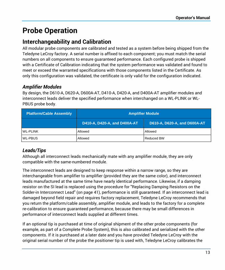
Amplifier Modules By design, the D610-A, D620-A, D600A-AT, D410-A, D420-A, and D400A-AT amplifier modules and interconnect leads deliver the specified performance when interchanged on a WL-PLINK or WL-PBUS probe body.
Platform/Cable Assembly Amplifier Module
D410-A, D420-A, and D400A-AT D610-A, D620-A, and D600A-AT
WL-PLINK Allowed Allowed
WL-PBUS Allowed Reduced BW
Leads/Tips Although all interconnect leads mechanically mate with any amplifier module, they are only compatible with the same-numbered module.
The interconnect leads are designed to keep response within a narrow range, so they are interchangeable from amplifier to amplifier (provided they are the same color), and interconnect leads manufactured at the same time have nearly identical performance. Likewise, if a damping resistor on the SI lead is replaced using the procedure for "Replacing Damping Resistors on the Solder-in Interconnect Lead" (on page 41), performance is still guaranteed. If an interconnect lead is damaged beyond field repair and requires factory replacement, Teledyne LeCroy recommends that you return the platform/cable assembly, amplifier module, and leads to the factory for a complete re-calibration to ensure guaranteed performance, because there may be small differences in performance of interconnect leads supplied at different times.
If an optional tip is purchased at time of original shipment of the other probe components (for example, as part of a Complete Probe System), this is also calibrated and serialized with the other components. If it is purchased at a later date and you have provided Teledyne LeCroy with the original serial number of the probe the positioner tip is used with, Teledyne LeCroy calibrates the

WaveLink Low Bandwidth (4, 6 GHz) Differential Probe
14
positioner tip to your existing components and supplies a file on a USB memory stick for installation on your oscilloscope. Follow the instructions provided with the file and memory stick in order to load this file and ensure proper calibrated performance with your existing probe components.
Handling the Probe The WaveLink series probe is a precision test instrument. Exercise care when handling and storing the probe. Always handle the probe by the platform/cable assembly. Avoid putting excessive strain on the cables or bending them sharply.
CAUTION. The tips of the WaveLink probes are sensitive to Electrostatic Discharge (ESD). Always follow anti-static procedures (wear wrist strap, etc.) when using or handling the probe.
CAUTION. Prevent damage to the flexible tips. Store the leads in the plastic protective storage case, and always attach the plastic cover to the Adjustable Tip module when not in use.
Connecting an Amplifier Module to a Platform/Cable Assembly Attach an amplifier module to the platform/cable by aligning the connectors of the module with the receptacles in the platform/cable assembly and pressing the two together. Finger tighten the assembly by rotating the threaded collar onto the module.
CAUTION. Do not use pliers or any other tools to tighten the collar.
Remove the module by loosening the threaded collar and pulling the two assemblies apart.
The same procedures may be used for the Adjustable Tip module.

Operator’s Manual
15
Attaching Adjustable Tip or Amplifier Module
Connecting Interconnect Leads/Tips to the Amplifier Align the flat side of the lead connector housing with the flat side of the amplifier and press together. Match the color-coding on the connector housing with the color-coding on the corresponding probe tip and press together.
SI, SP, QC, and PT Interconnect Lead

WaveLink Low Bandwidth (4, 6 GHz) Differential Probe
16
QuickLink Probe Adapter and QL-SI Lead
Hi-Temp Interconnect Lead

Operator’s Manual
17
Positioning Interconnect Leads Normally, the performance of the interconnect leads is not affected by the position of the amplifier module. They can be mounted straight upright or on an angle.
However, when it is necessary to mount the module parallel to the board, the maximum performance is obtained when the “+” sign (printed near the positive input tip) is facing up.
The flexible cable connecting the tip of the lead to the amplifier module is reasonably insensitive to placement, but can be affected by large signal emitters on the device under test, so avoid placing it near these types of signals.
Connecting the Probe to an Oscilloscope The WL-PLINK platform/cable assembly has been designed for use with the ProLink interface of Teledyne LeCroy oscilloscopes. The WL-PBUS is designed for use with the ProBus interface of Teledyne LeCroy oscilloscopes.
Attach the platform/cable assembly to the instrument by aligning the connector with the input and pushing the interface toward the instrument.
On the WL-PLINK assembly, you will hear a click when the connector latches to the test instrument. Tighten the thumbscrews to secure the assembly to the instrument. Do not overtighten the thumbscrews.
To remove the WL-PLINK assembly from the instrument, loosen the thumbscrews and move the connector up and down while gently pulling until a click is heard. This click indicates the assembly is detached from the instrument.
Thumbscrews are not provided on the WL-PBUS assembly. Disconnect the WL-PBUS assembly by pulling the connector head from the interface.
Connecting the Probe to the Test Circuit For all modules and interconnect leads/tips, positive voltages applied to the + input relative to the – input deflects the oscilloscope trace towards the top of the screen.
Exercise care when connecting the probe to the test circuit to maintain the high frequency capability of the probe in measurement applications. Increasing the parasitic capacitance or inductance in the input path may introduce a ring, or slow the rise time of fast-rising signals. Any extension of the signal path with extra wire leads, etc. adversely affects the probe's performance.
A ground connection is generally not required for most probing applications. Refer to Probe Grounding (on page 25) for more information.

WaveLink Low Bandwidth (4, 6 GHz) Differential Probe
18
Solder-In Lead Using a small soldering iron, attach the free wires of the two, pre-installed resistors to the runs or pad test points on the board under test.
PROPER SI LEAD POSITIONING Solder-in tips should be positioned with the resistor side facing upright (away from the PCB plane). Keep a 45 degree angle between the SI tip ends and the PCB plane.
Measuring with SI Interconnect Lead
CAUTION: The resistors are small in order to maintain high-frequency performance. However, they are not sturdy enough to bear the weight of the probe module. It should be supported by other means. A positioning tool such as the Board Clip, the Probe Tip Retaining Clip, or EZ Probe positioner can be used to support the probe.
PROPER RESISTOR SOLDERING PROCEDURE The goal is to get the resistor bodies to be parallel and the tips bent to sit on the test board traces.

Operator’s Manual
19
1. Bend the resistor bodies to position them parallel.
2. Bend the tips in toward the center. Make the bend as close to the resistor body as possible. Bend them to about 60° from straight.
3. At this point, the leads can be bent out from their midpoints (making them parallel to each other).
4. Perform a final check to ensure proper lead spacing and compare them to the trace spacing on the PCB.

WaveLink Low Bandwidth (4, 6 GHz) Differential Probe
20
Quick Connect Lead The Quick Connect (QC) lead can be used in applications requiring the probe to be moved to multiple test points.
To accurately position the resistors for soldering, first plug one end directly into the special connector mounted on the probe input board. Then, position the tip and solder the other end of the resistor to the testing point. Repeat this process when installing resistors on other test points.
A positioning tool like the Probe Tip Retaining Clip can be used to aid in holding the QC lead in place for soldering.
NOTE: For maximum performance, do not extend the resistor wires or use different resistors.
Measuring with the QC Interconnect Lead
CAUTION: Do not confuse the Quick Connect lead with the Square Pin lead. The Square Pin lead is clearly labeled with the initials “SP” printed on the square pin receptacle housing. The Quick Connect lead has been designed to accept only the wire diameter of the small damping resistors, not the 0.025” thickness of the square pin. Inserting square pins into the connector of the Quick Connect Lead could damage the wire receptacle of the lead.

Operator’s Manual
21
Square Pin Lead Insert the head of the Square Pin lead directly over standard 0.025” square pins mounted on 0.100” centers.
Measuring with the SP Interconnect Lead
Square Pin Header Dimensions

WaveLink Low Bandwidth (4, 6 GHz) Differential Probe
22
The system bandwidth and rise time are limited by the Square Pin lead because of the inherent inductance of the square pins themselves.
Keep the highest possible performance by keeping the parasitic inductance under control. Also, make good electrical connections by not using any square pins longer than 2.79 mm (0.110”) or shorter than 2.54 mm (0.100”).
Square Pin length
Positioner Tip (Browser) Various attachments and extenders are supplied with the PT, allowing it to be easily held while browsing or connected to a mounting device. Using these attachments, the tip can be positioned in many different ways to make probing possible in tight geometries.
Rotate the thumbwheel to adjust the tip spacing from 0 to 3.5 mm (0 to 0.14") in a direction perpendicular to the thumbwheel rotation. There is a positive stop on the thumbwheel to prevent it from being rotated too far in either direction.

Operator’s Manual
23
The tip is a pogo-pin assembly and is spring-mounted to accommodate 0.6mm of Z-Axis compliance. This aids in applications where more than one positioner tip is required to make measurements in a crowded area and the tips need to be mounted at an angle to the board under test.
Exercise care when using the PT. Avoid applying excessive lateral pressure on the tip as it may break. Do not use the tip to scrape the circuit. If the tip does break, it may be replaced in the socket. If the socket also breaks, a new socket can be soldered onto the tip. See Replacing Spring-Loaded Tips and Tip Sockets on Positioner Tips (on page 43).
Adjustable Tip Module (-AT) The spacing of the flexible, nickel-titanium alloy tips can be adjusted by rotating the knurled thumbscrew on the top of the module to accommodate different test point spacing from less than 0.1 mm to > 3 mm.
Adjusting the spacing of the tips
For accurate measurements, both the + and – inputs must always be connected to the test circuit.
NOTE: When making differential measurements, both tips need to make good contact. The best way to accomplish this is to place one tip on one test point, apply a little pressure and by rotating the probe body slightly, place the other tip on the other test point. Assure good contact and apply enough pressure to bend the tips just a bit.
Excessive bending of these tips may damage the module beyond repair. However, the tips are flexible enough to allow both tips to make good contact with the circuit under test even when the probe is slightly rotated with respect to the circuit under test.
NOTE: Always support the probe to prevent too much stress on the pins of the Adjustable Tip Module.

WaveLink Low Bandwidth (4, 6 GHz) Differential Probe
24
HiTemp SI Lead When using the Dxx0-SI-HiTemp lead in extreme conditions, the Tip Retaining Clip is rated to 100 °C and adhesives are rated to 90 °C. The primary function of the Tip Retaining Clip is to position the resistor leads when soldering the resistors to the test points.
QL-SI Tip Attach QL-SI Tips as you would any solder-in lead tip.
Once soldered to the board, the QL-SI tips can be switched from the WaveLink probe to an HDA125 High-speed Digital Analyzer by pulling the tip head from the amplifier and plugging it into the digital leadset pod, or vice versa.
Switching QL-SI tips between WaveLink probe and HDA125

Operator’s Manual
25
Probe Grounding In most cases, when the common mode portion of the signal consists mainly of lower frequencies, the probe does not need to be connected to the ground of the circuit under test. This minimizes the effects of ground loop currents. Any signal corruption caused by not having the probe connected to ground of the signal under test is common to both inputs and is rejected by the differential operation of the probe. Find out if a ground lead is necessary by making a measurement with and without a ground lead. Use the method that provides the least signal corruption.
However, capacitive coupling from AC mains may cause truly floating devices (like battery operated devices) to exceed the common mode range. In such cases, or in environments with high RF ambient noise, it is recommended to connect the probe ground to the device under test.
CAUTION: Always use a ground lead when testing floating circuits. Floating circuitry (e.g., circuits powered from laboratory bench power supplies which normally have floating outputs) may damage the probe by exceeding the common mode input voltage.
Connect the plug of the ground lead to the receptacle located on the side of the amplifier/adjustable tip module body.
In floating devices, attach the probe ground lead to the DUT’s reference or common voltage.
In high RF ambient noise environments, attach the probe ground lead to a good RF ground near the point where the signal is being measured.
WaveLink Low Bandwidth (4, 6 GHz) Differential Probe
26
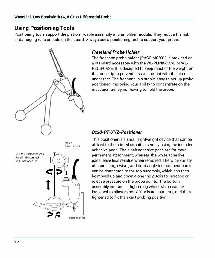
Using Positioning Tools Positioning tools support the platform/cable assembly and amplifier module. They reduce the risk of damaging runs or pads on the board. Always use a positioning tool to support your probe.
FreeHand Probe Holder The freehand probe holder (PACC-MS001) is provided as a standard accessory with the WL-PLINK-CASE or WL-PBUS-CASE. It is designed to keep most of the weight on the probe tip to prevent loss of contact with the circuit under test. The freehand is a stable, easy-to-set-up probe positioner, improving your ability to concentrate on the measurement by not having to hold the probe.
Dxx0-PT-XYZ-Positioner This positioner is a small, lightweight device that can be affixed to the printed circuit assembly using the included adhesive pads. The black adhesive pads are for more permanent attachment, whereas the white adhesive pads leave less residue when removed. The wide variety of short, long, swivel, and right angle interconnect parts can be connected to the top assembly, which can then be moved up and down along the Z-Axis to increase or release pressure on the probe points. The bottom assembly contains a tightening wheel which can be loosened to allow minor X-Y axis adjustments, and then tightened to fix the exact probing position.

Operator’s Manual
27
EZ Probe Positioner The Cascade Microtech EZ-Probe Positioner is available as an optional accessory. It provides stable, accurate positioning in the X-Y-Z axes. The unique 3:1 motion reduction joystick allows simple, precise positioning of the attached probe in both the horizontal and vertical measuring plane. The probe has a fully-articulating arm, providing 30 cm (12 inch) reach in virtually any direction.
The XYZ joystick has separate friction controls allowing independent X-Y plane or Z-Axis movement and is especially useful when combined with the positioner tip.
The EZ-Probe Positioner comes with a vacuum mounted base to keep the probe in place in any test environment. However, the solid base is heavy enough that the positioner can be used without the vacuum.
EZ PROBE POSITIONER USING DX10-PT AND DX20-PT
Attach the probe by first removing the screws holding the top plate to the V-shaped probe holder. Rest the Long Interconnect Extender in the V-shaped groove, and fasten the top plate to the holder, using the removed screws (as follows). Then, insert the Dx10 or Dx20-PT onto the Long Interconnect Extender.
NOTE: Do not over-tighten the screws.
Once the probe has been attached, loosen the knob on the EZ-Probe Positioner arm and position the probe close to the test point. Tighten the knob and use the joystick to fine position the probe.

WaveLink Low Bandwidth (4, 6 GHz) Differential Probe
28
EZ PROBE POSITIONER USING DX00A-AT
Attach the probe by first removing the screws holding the top plate to the V-shaped probe holder. Insert the end of the platform/cable assembly and tighten the screws holding the top plate to secure the probe.
Tip Retaining Clip The Tip Retaining Clip (PK600ST-3) is an aid for holding the SI Interconnect Leads in place while making measurements or when soldering the damping resistors to the test points of the board under test.
NOTE: When using the Dxx0-SI-HiTemp lead in extreme conditions, the Tip Retaining Clip is rated to 100 °C and adhesives are rated to 90 °C.
The Clip comes standard with the Differential Amplifier Small Tip Modules (on page 9) along with a set of 10 white and 10 black Adhesive Pads (Dxx0-PT-TAPE) used for mounting the clip to the board.

Operator’s Manual
29
FASTENING THE CLIP TO THE BOARD Fasten the clip to the board by removing the small piece of protection paper from one side of the adhesive pad and mount the pad to the underside of the clip. If necessary, use alcohol to clean the section of the board where the clip is mounted to remove any grease or flux residue.
Connecting the SI Module Using the Tip Retaining Clip
Remove the protective paper from the other side of the adhesive pad and mount the clip to the desired location on the board. Apply pressure to the clip for at least several seconds to assure proper adhesion (shown previous).
The adhesive pad with the tab is still be visible and stays attached to the adhesive pad. The tab is used to remove the clip from the board.
NOTE: Maximum strength of the adhesive pad is obtained after about 30 minutes.

WaveLink Low Bandwidth (4, 6 GHz) Differential Probe
30
MOVING AND POSITIONING Always apply pressure to the pad (as follows) to prevent any shifting while bending the arms and/or moving the probe adapter portion of the clip (typically done while positioning or attaching the probe). This is especially important if moving and positioning before the adhesive pads have properly cured.
Applying pressure when adjusting the probe holder
ATTACHING THE PROBE Attach the probe by positioning the cable of the module on top of the clip and sliding the input board of the module into the grooves. While moving the probe into position for measurement, apply pressure to the mounting pad to prevent the adhesive pad from moving and losing its adhesion.
Attaching the Probe
Operator’s Manual
31
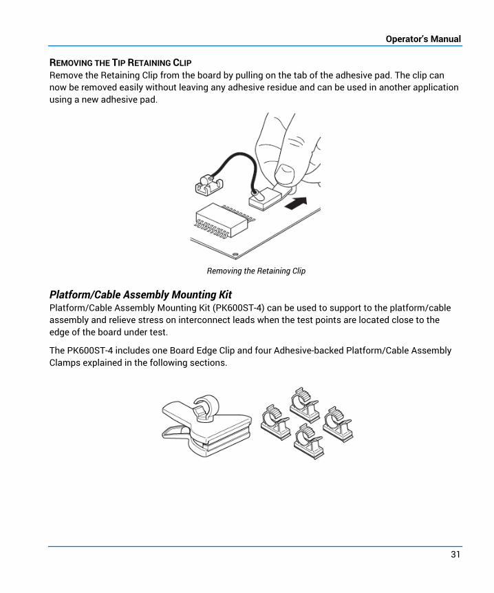
REMOVING THE TIP RETAINING CLIP Remove the Retaining Clip from the board by pulling on the tab of the adhesive pad. The clip can now be removed easily without leaving any adhesive residue and can be used in another application using a new adhesive pad.
Removing the Retaining Clip
Platform/Cable Assembly Mounting Kit Platform/Cable Assembly Mounting Kit (PK600ST-4) can be used to support to the platform/cable assembly and relieve stress on interconnect leads when the test points are located close to the edge of the board under test.
The PK600ST-4 includes one Board Edge Clip and four Adhesive-backed Platform/Cable Assembly Clamps explained in the following sections.

WaveLink Low Bandwidth (4, 6 GHz) Differential Probe
32
BOARD EDGE CLIP The Board Edge Clip can be used to give support to the probe and Interconnect Lead when the test points are located close to the edge of the board under test. It's also useful for holding the probe assembly while soldering the solder-in interconnect lead to your device under test.
Slide the probe cable into the clamp opening and move the probe so that the probe’s strain relief is located in the opening. Close the clamp.
Slide the Probe into the Board Edge Clip
Insert the probe body into the board edge clip and position the clamp as desired.

Operator’s Manual
33
ADHESIVE BACKED PLATFORM/CABLE ASSEMBLY CLAMPS The Adhesive Backed Platform/Cable Assembly Clamp provides additional support to the Platform/Cable Assembly and Interconnect Lead anywhere on the board under test.
Connection Guides Probe connection guides are designed to make it easy to electrically isolate the two probe tips when browsing. They also greatly reduce accidental and unwanted contact across probe points.
Before attaching connection guides, clean the PCA assembly area with IPA or another cleaner to remove oils. Then, apply with a light pressure, release, and let set for one hour.
Controlling the Probe from the Oscilloscope When the fully assembled probe is connected to an X-Stream oscilloscope, the oscilloscope recognizes the probe and opens the respective Channel (Cx) setup dialog.
Channel dialog with tab corresponding to attached probe (amplifier) model
Behind the Cx dialog is a dialog of controls for the probe (the name varies based on the amplifier module you have attached). The Attributes section of the Probe dialog includes information such as amplifier bandwidth and probe attenuation.
Probe dialog shows attributes of attached probe

WaveLink Low Bandwidth (4, 6 GHz) Differential Probe
34
Power Control Select the Power On checkbox to turn on power to the probe tip.
Newer, X-Stream model oscilloscopes feature Power Control. Power Control allows intermittent operation of a small tip modules and probe tip combinations during testing at elevated ambient temperatures to prevent overheating of the probe; as, for example, when testing the operation of test circuits in temperature chambers.
The intent of this feature is to keep the probe tip power off during the time when the chamber temperature is changing between tests. When the chamber temperature has stabilized and measurements are ready to be taken, the probe is powered on to facilitate measurements. The probe is then powered down while the chamber temperature is changing for the next test.
The time the probe can be operated at these elevated temperatures is a function of airflow, thermal conductivity of the probe in that environment, etc. For a starting estimate on time vs. temperature refer to the following table.
When the probe operates at an elevated ambient temperature, the wave shape is correct, but because it is outside the specified temperature range the amplitude may be uncalibrated.
If over-temperature does occur when used with a Teledyne LeCroy X-Stream oscilloscope, the probe automatically turns off the power applied to the probe, and the AutoColor ID on the probe body flashes in red. In addition, a warning message appears on the oscilloscope’s screen. When cooled down, reset the power again.
Approximate Operating Time at Temperature for the D400A-AT and D600A-AT Temperature °C Time
Up to 40 Continuous
40 to 55 40 minutes
55 to 65 18 minutes
65 to 75 30 seconds
75 to 85 15 seconds

Operator’s Manual
35
AutoColor ID
AutoColor ID LED indicators
The AutoColor ID LEDs built into the platform/cable assembly immediately inform you of three conditions related to the probe:
• Input channel―the LED illuminates in the default color of the channel to which the probe is connected.
• Component compatibility―when the amplifier module is compatible with the platform/cable assembly to which it is connected, the green LED illuminates for about one second after the probe is connected to the oscilloscope. A continuous red light indicates the components are not compatible.
• Over-temperature state―If the probe is over-temperature, the red LED flashes. The probe is automatically shut down in this state (see Power Control). Unless the shut-down is caused by over-temperature, all LEDs are normally off when probe is powered down.
In some applications it may be desirable to turn the probe’s AutoColor ID off by deselecting the LED Active checkbox on the Probe dialog.
Tip Select The Probe dialog contains a Tip Select field. Select the tip you’re using before applying any other pre-processing functions to the input signal.
CAUTION: It is crucial to make the tip selection on this field as it results in the amplifier and tip combination having the response calibrated for at the factory. Failure to select the proper tip may result in inaccurate measurements. If you do not see the tip among the selections, return the probe to the Teledyne LeCroy factory for re-calibration.
WaveLink Low Bandwidth (4, 6 GHz) Differential Probe
36
AutoZero WaveLink probes incorporate an AutoZero function to remove any DC offset from the probe. This function is available when the probe is used with Teledyne LeCroy’s X-Stream oscilloscopes, and must be invoked by the user.
After several minutes of warm-up, or when the probe is exposed to a large shift in ambient temperature, some DC offset may occur, and an AutoZero cycle should be initiated.
Start an AutoZero cycle by removing the probe from the circuit under test and touching the AutoZero button on the Probe dialog.
CAUTION: Remove all inputs from the probe before initializing AutoZero.
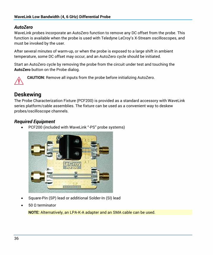
Deskewing The Probe Characterization Fixture (PCF200) is provided as a standard accessory with WaveLink series platform/cable assemblies. The fixture can be used as a convenient way to deskew probes/oscilloscope channels.
Required Equipment • PCF200 (included with WaveLink “-PS” probe systems)
• Square-Pin (SP) lead or additional Solder-In (SI) lead
• 50 Ω terminator
NOTE: Alternatively, an LPA-K-A adapter and an SMA cable can be used.
Operator’s Manual
37
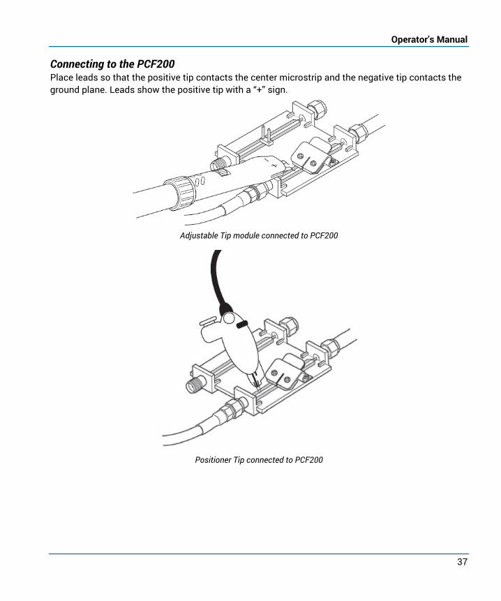
Connecting to the PCF200 Place leads so that the positive tip contacts the center microstrip and the negative tip contacts the ground plane. Leads show the positive tip with a “+” sign.
Adjustable Tip module connected to PCF200
Positioner Tip connected to PCF200

WaveLink Low Bandwidth (4, 6 GHz) Differential Probe
38
For solder-in leads, press the black plastic tab on the PCF200 to open the clamp, placing the resistor tips under the clamp so that the + tip contacts the center microstrip and the – tip contacts the ground plane. Release the clamp so it holds the wires securely in place.
SI, QC, or QL-SI tips connected to PCF200
Place the Square Pin lead over the pins on the second circuit.
SP Lead connected to PCF200

Operator’s Manual
39
Methodology Before beginning the deskew procedure, warm the oscilloscope for at least 20 minutes.
1. Connect the PCF200 to the oscilloscope’s fast edge output. The PCF200 fixture has two different signal paths that can be used, depending on the type of probe tip being used for the measurement:
• The upper signal path is for deskewing Solder-In (SI) lead, Quick-Connect (QC) lead, QL-SI leads, Positioner Tip (PT), and Adjustable Tip (AT) module.
• The lower circuit is for Square-Pin (SP) leads.
Depending upon which probe tip is being used, connect the appropriate signal path to the fast edge output. For ease of connectivity, it is recommended to use the SP tip. However, as long as you use the same tip to deskew each probe, it does not matter which style of probe tip you use.
2. Connect probes electrically in a single-ended arrangement using their designated area on the fixture.
• The positive side of the probe must be connected to the signal trace (in between the two white strips), while the negative side is connected to the ground plane (outside of the white strips). The positive polarity is indicated on the tip of the probe by a plus sign.
• In order to minimize reflection, apply a 50 Ω terminator to the end of the signal path in use. If a 50 Ω terminator is not available, an SMA cable can be used to terminate the PCF200 to one of the oscilloscope’s outputs.
3. Touch the Trigger descriptor box to open the Trigger dialog. Set the oscilloscope Trigger Type to “Edge”, the Trigger Source to “FastEdge”.
4. Touch the Timebase descriptor box to open the Timebase dialog. Set the Timebase Delay to zero.
WaveLink Low Bandwidth (4, 6 GHz) Differential Probe
40
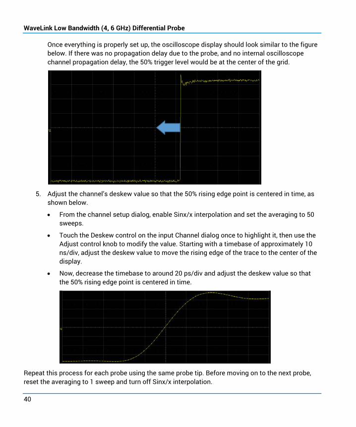
Once everything is properly set up, the oscilloscope display should look similar to the figure below. If there was no propagation delay due to the probe, and no internal oscilloscope channel propagation delay, the 50% trigger level would be at the center of the grid.
5. Adjust the channel’s deskew value so that the 50% rising edge point is centered in time, as shown below.
• From the channel setup dialog, enable Sinx/x interpolation and set the averaging to 50 sweeps.
• Touch the Deskew control on the input Channel dialog once to highlight it, then use the Adjust control knob to modify the value. Starting with a timebase of approximately 10 ns/div, adjust the deskew value to move the rising edge of the trace to the center of the display.
• Now, decrease the timebase to around 20 ps/div and adjust the deskew value so that the 50% rising edge point is centered in time.
Repeat this process for each probe using the same probe tip. Before moving on to the next probe, reset the averaging to 1 sweep and turn off Sinx/x interpolation.
Operator’s Manual
41
Maintenance Cleaning Clean the exterior of the probe and cable using a soft cloth moistened with water. Do not use abrasive agents, strong detergents, or other solvents as these may damage the probe.
CAUTION: The probe case is not sealed and should never be immersed in any fluid.
Replacing Damping Resistors on the SI Lead A set of 20 replacement damping resistors have been supplied with the Solder-In Interconnect Lead.
NOTE: Do not confuse the SI module damping resistors with the Quick Connect lead resistors. The SI replacement damping resistors are smaller. Resistors used in the D610-A, D620-A, D410-A, and D420-A have different values from those used in the older D350ST.
The external damping resistors locate the tip resistance as close to the device under test as possible, which minimizes tip inductance and capacitance and provides very favorable loading characteristics. However, these resistors are subject to mechanical stress and may periodically need to be replaced even if proper stress-relief precautions are taken. Replacement damping resistors are included with the probe, and replacement of these resistors is simple. Resistors are pre-cut to the right lead lengths, so all that is required is removal and attachment of the new resistor.
Follow these steps to correctly remove the damaged damping resistors and to solder a new resistor to your tip. It is assumed that the person performing the resistor replacement is familiar with fine-pitch soldering techniques.
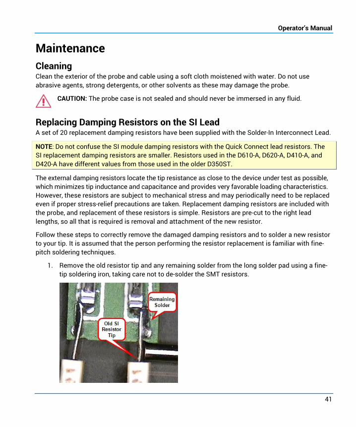
1. Remove the old resistor tip and any remaining solder from the long solder pad using a fine-tip soldering iron, taking care not to de-solder the SMT resistors.
WaveLink Low Bandwidth (4, 6 GHz) Differential Probe
42
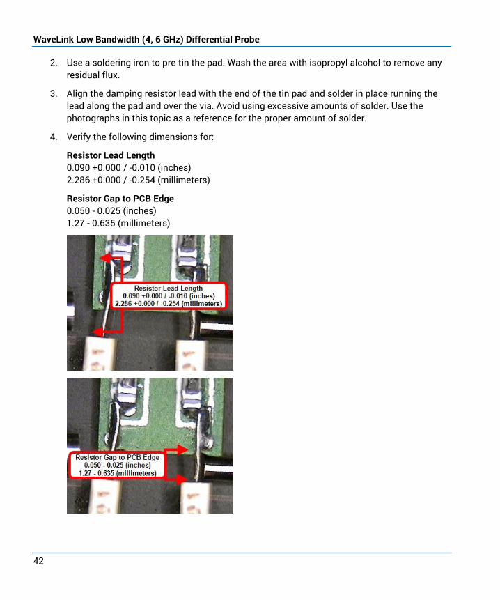
2. Use a soldering iron to pre-tin the pad. Wash the area with isopropyl alcohol to remove any residual flux.
3. Align the damping resistor lead with the end of the tin pad and solder in place running the lead along the pad and over the via. Avoid using excessive amounts of solder. Use the photographs in this topic as a reference for the proper amount of solder.
4. Verify the following dimensions for:
Resistor Lead Length 0.090 +0.000 / -0.010 (inches) 2.286 +0.000 / -0.254 (millimeters)
Resistor Gap to PCB Edge 0.050 - 0.025 (inches) 1.27 - 0.635 (millimeters)

Operator’s Manual
43
Replacing Tips and Sockets on the Positioner Tip Replacing Spring-Loaded Tips A set of four replacement spring-loaded tips have been supplied with the Dx10-PT and Dx20-PT Positioner Tips. Under normal usage, the tips should last a very long time. However, in the event of breakage or damage, they can be easily replaced.
First, adjust the tip spacing to its maximum open position. Then, remove the old tip from the socket and insert a new tip, taking care to orient it in the correct direction. While replacing tips, mount the Dx10/Dx20-PT in a clamp, taking care to not adjust too tightly.
Replacing Tip Sockets Two replacement tip sockets have been supplied with the Dx10-PT and Dx20-PT Positioner Tips. Under normal usage, the tip sockets should not need replacement. However, in the event of breakage or damage, new sockets can be soldered into place using the following steps:
1. Secure the positioner tip in a clamp to immobilize it while working. Using an appropriate fine-tip soldering iron for low mass components, apply heat and remove the damaged socket from the positioner tip circuit board.
2. Clean off the pad using the soldering iron. Clean oils and dirt in the area using deionized or distilled water and isopropyl alcohol. Inspect the pad for damage - damaged or loose sockets do not adhere properly.
3. Tin the pad using a no clean solder (shown below). Tin thickness should be .010” to .015” (2.5 to 4 mm).

WaveLink Low Bandwidth (4, 6 GHz) Differential Probe
44
4. Locate the socket so the closed end is slightly overhanging the end of the pad. This prevents solder from flowing into the socket insert hole. Align the socket sides with the pad sides and solder as shown. Leave proper clearance between the socket and pad sides when soldering.
5. Finally, clean the newly soldered assembly with deionized or distilled water.
Operator’s Manual
45
Returning a Product for Service Contact your local Teledyne LeCroy service center for calibration or other service. If the product cannot be serviced on location, the service center will give you a Return Material Authorization (RMA) code and instruct you where to ship the product. All products returned to the factory must have an RMA.
Return shipments must be prepaid. Teledyne LeCroy cannot accept COD or Collect shipments. We recommend air-freighting. Insure the item you’re returning for at least the replacement cost.
1. Remove all accessories from the device. If you need to return a D610-A, D620-A, D410-A, or D420-A module, be sure to include all Interconnect Leads and Tips (SI, QC, SP, PT). Do not include the manual.
2. Pack the product in its case, surrounded by the original packing material (or equivalent).
3. Label the case with a tag containing:
• The RMA
• Name and address of the owner
• Product model and serial number
• Description of failure or requisite service
4. Pack the product case in a cardboard shipping box with adequate padding to avoid damage in transit.
5. Mark the outside of the box with the shipping address given to you by Teledyne LeCroy; be sure to add the following:
• ATTN: <RMA code assigned by Teledyne LeCroy>
• FRAGILE
6. If returning a product to a different country:
• Mark the shipment as a "Return of US manufactured goods for warranty repair/recalibration."
• If there is a cost for the service, list the cost in the Value column and the original purchase price "For insurance purposes only."
• Be very specific about the reason for shipment. Duties may have to be paid on the value of the service.

WaveLink Low Bandwidth (4, 6 GHz) Differential Probe
46
Service Options Defective probes or probe tip modules must be returned to a Teledyne LeCroy service facility for diagnosis and repair. Defective products under warranty are repaired or replaced.
Probes are warranted for a period of one year from shipment. The following extended warranty and service plans are available.
NOTE: For warranted accuracy, amplifiers must be returned for calibration with leads.
Service Option Product Code
Three-Year Warranty for D600A-AT D600A-AT-W3
Three-Year Warranty for D400A-AT D400A-AT-W3
Three-Year Warranty for D610-A D610-A-W3
Three-Year Warranty for D620-A D620-A-W3
Three-Year Warranty for D410-A D410-A-W3
Three-Year Warranty for D420-A D420-A-W3
Five-Year Warranty for D600A-AT D600A-AT-W5
Five-Year Warranty for D400A-AT D400A-AT-W5
Five-Year Warranty for D610-A D610-A-W5
Five-Year Warranty for D620-A D620-A-W5
Five-Year Warranty for D410-A D410-A-W5
Five-Year Warranty for D420-A D420-A-W5
Three-Year Warranty and Annual NIST Calibration D600A-AT-T3
Three-Year Warranty and Annual NIST Calibration D400A-AT-T3
Three-Year Warranty and Annual NIST Calibration D610-A-T3
Three-Year Warranty and Annual NIST Calibration D620-A-T3
Three-Year Warranty and Annual NIST Calibration D410-A-T3
Three-Year Warranty and Annual NIST Calibration D420-A-T3
Five-Year Warranty and Annual NIST Calibration D600A-AT-T5
Five-Year Warranty and Annual NIST Calibration D400-A-AT-T5
Five-Year Warranty and Annual NIST Calibration D610-A-T5
Five-Year Warranty and Annual NIST Calibration D620-A-T5
Five-Year Warranty and Annual NIST Calibration D410-A-T5
Five-Year Warranty and Annual NIST Calibration D420-A-T5

Operator’s Manual
47
Service Option Product Code
Three-Year Annual NIST Calibration D600A-AT-C3
Three-Year Annual NIST Calibration D400A-AT-C3
Three-Year Annual NIST Calibration D610-A-C3
Three-Year Annual NIST Calibration D620-A-C3
Three-Year Annual NIST Calibration D410-A-C3
Three-Year Annual NIST Calibration D420-A-C3
Five-Year Annual NIST Calibration D600A-AT-C5
Five-Year Annual NIST Calibration D400A-AT-C5
Five-Year Annual NIST Calibration D610-A-C5
Five-Year Annual NIST Calibration D620-A-C5
Five-Year Annual NIST Calibration D410-A-C5
Five-Year Annual NIST Calibration D420-A-C5
NIST Traceable Calibration with Test Data* (one module)
D600A-AT-CCNIST
D400A-AT-CCNIST
D610-A-CCNIST
D620-A-CCNIST
D410-A-CCNIST
D420-A-CCNIST
*CCNIST NIST traceable calibration with test data is available for D610-A, D620-A, D410-A, D420-A, D600A-AT,and D400A-AT differential amplifier modules only when ordered with either a WL-PLINK-CASE or WL-PBUS-CASE probe platform.

WaveLink Low Bandwidth (4, 6 GHz) Differential Probe
48
Consumables and Replacement Parts
Description Image Replacement Product Code
Positioner Tip with Accessories
RK-Dx10-PT-Kit RK-Dx20-PT-Kit
Positioner Tip
(included as part of Dxxx-PT-Kit)
Dx10-PT (for D610-A and D410-A) Dx20-PT (for D620-A and D420-A)
Pogo Pin Tips for PT
(included as part of Dxxx-PT-Kit)
Dxx0-PT-Tips (Qty. 4)
Pogo Tip Connection Guides
(included as part of Dxxx-PT-Kit)
Dxx0-PT-Guides

Operator’s Manual
49
Description Image Replacement Product Code
XYZ Positioner
(included as part of D6x0-PT-Kit/ D4x0-PT-Kit)
Dxx0-PT-XYZ-Positioner
Adhesive Tape for XYZ Positioner
(included as part of D6x0-PT-Kit and D4x0-PT-Kit)
Dxx0-PT-Tape (10 pieces each)
Browser Wand for Positioner Tip
(included as part of D6x0-PT-Kit and D4x0-PT-Kit)
Dxx0-PT-Wand
Interlock Pieces for Positioner Tip
(included as part of D6x0-PT-Kit and D4x0-PT-Kit)
Dxx0-PT-Interlock (6 pieces)
Swivel for Positioner Tip
(included as part of
Dxx0-PT-Swivel

WaveLink Low Bandwidth (4, 6 GHz) Differential Probe
50
Description Image Replacement Product Code
D6x0-PT-Kit and D4x0-PT-Kit)
Solder-In Tips
(included as part of D6x0-A and D4x0-A)
PKxx0-SI (for D6x0 and D4x0) (Qty. 5)
Solder-In Lead
(with PK600ST-3, included as part of D6x0-A and D4x0-A)
Dx10-SI (for D610-A and D410-A) Dx20-SI (for D620-A and D420-A)
Square Pin Lead
(with Spare Resistors, included as part of D6x0-A and D4x0-A)
Dx10-SP (for D610-A and D410-A) Dx20-SP (for D620-A and D420-A)

Operator’s Manual
51
Description Image Replacement Product Code
Quick Connect Lead (with Spare Resistors, included as part of D6x0-A and D4x0-A)
Dx10-QC (for D610-A and D410-A) Dx20-QC (for D620-A and D420-A)
HiTemp-SI Lead
(with Spare Resistors)
Dx10-SI-HiTemp (for D610-A and D410-A) Dx20-SI-HiTemp (for D620-A and D420-A)
HiTemp Cable
Dx10-Cable-HiTemp (for D610-A and D410-A) Dx20-Cable-HiTemp (for D620-A and D420-A) (1 Paired Cable)

WaveLink Low Bandwidth (4, 6 GHz) Differential Probe
52
Description Image Replacement Product Code
QuickLink Adapter
Dx10-QL (for D610-A and D410-A) Dx20-QL (for D620-A and D420-A)
QL-SI Tips (1- or 9-tip pack)
Dx10-1QL-SI/Dx10-9QL-SI (for D610-A and D410-A) Dx20-1QL-SI/Dx20-9QL-SI (for D620-A and D420-A)
Solder-In Probe Holder Kit (with 2 tip retaining clips and 1 set of adhesive tape, included as part of D6x0-A and D4x0-A)
PK600ST-3
Ground Lead
(Included as part of D6x0-A and D4x0-A)
PACC-LD005 (Qty. 4)
Ground Clip
(Included as part of D6x0-A and D4x0-A)
PK006-4 (Qty. 2)
Platform/Cable Assembly Mounting Kit (With 1 Board Clip and 4 Clamps, Included with WL-PLINK-CASE and WL-PBUS-CASE)
PK600ST-4

Operator’s Manual
53
Description Image Replacement Product Code
Probe Deskew Fixture
(Included with WL-PLINK-CASE and WL-PBUS-CASE)
PCF200
Freehand Probe Holder
(Included with WL-PLINK-CASE and WL-PBUS-CASE)
PACC-MS001
Deluxe Soft Carrying Case (Included with WL-PLINK-CASE and WL-PBUS-CASE)
SAC-03
WaveLink Low Bandwidth (4, 6 GHz) Differential Probe
54
Description Image Replacement Product Code
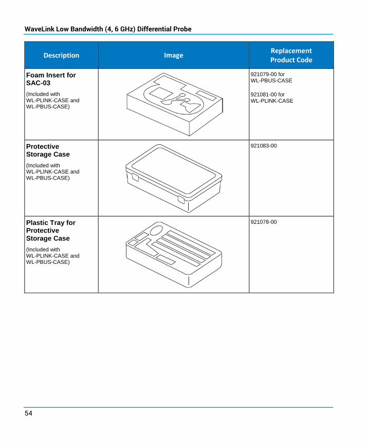
Foam Insert for SAC-03 (Included with WL-PLINK-CASE and WL-PBUS-CASE)
921079-00 for WL-PBUS-CASE 921081-00 for WL-PLINK-CASE
Protective Storage Case
(Included with WL-PLINK-CASE and WL-PBUS-CASE)
921083-00
Plastic Tray for Protective Storage Case (Included with WL-PLINK-CASE and WL-PBUS-CASE)
921078-00

Operator’s Manual
55
Performance Verification The following procedures can be used to verify basic operation and some of the warranted characteristics of the WaveLink Differential Probe.
The recommended calibration interval for differential probes is one year. Test results can be recorded on a photocopy of the "Performance Verification Test Record" provided at the end of this procedure.
Performance Verification can be completed without removing the probe covers or exposing the user to hazardous voltages. No adjustments are provided.
In the unlikely event a probe fails performance verification, it can be sent back to the local service center or the factory. For information on returning the probe, see "Returning a Product for Service" on page 45.
If the probe package includes multiple probe interconnect leads, the best practice is to complete the entire procedure for each probe interconnect lead. If more than one interconnect lead is being verified, copy and fill out a separate test record for each combination of platform/cable assembly, amplifier module, and interconnect lead.
If the probe package includes probe interconnect leads that are not serialized to the amplifier module and platform/cable assembly, then performance may not be verifiable.
NOTE: It is recommended that the Functional Test be performed prior to the Performance Verification Procedure to assure all other non-warranted functions perform as specified.

WaveLink Low Bandwidth (4, 6 GHz) Differential Probe
56
Functional Test The functional test can be used prior to the Performance Verification procedure to verify the basic operation of the WaveLink Differential Probe when used with a Teledyne LeCroy X-Stream oscilloscope.
1. Connect a module to a probe body (for example, a WL-PLINK with a D600A-AT), and then connect the body to Channel 1 of the oscilloscope.
The instant the probe is connected to the oscilloscope, the AutoColor ID LEDs should illuminate GREEN for less than 1 second, then change to the color of the channel to which the probe is connected, indicating the probe is compatible with the oscilloscope.
2. Verify the probe AutoColor ID indicates the proper channel by disconnecting the probe and reconnecting it to the other channels, confirming the proper color LED illuminates.
3. Reconnect the probe to channel 1. Turn on C1 trace.
4. Touch the C1 descriptor box to display the C1 setup dialog. Verify the correct probe model is shown on the tab following the C1 tab. (The D420-A-SI is shown in the examples here.)
5. Open the Probe dialog.

Operator’s Manual
57
6. Clear the Power On checkbox to verify the AutoColor ID LEDs turn OFF when probe power is OFF. Turn the power back ON by selecting the checkbox again.
NOTE: The LEDs might still be illuminated at low intensity when turned off.
7. Clear the Led On checkbox to verify the AutoColor ID LEDs turn OFF when probe power is still ON. Turn LEDs back ON by selecting the checkbox again.
8. Set up the calibrator for performing the functional tests:
• Choose Utilities > Utilities Setup from the menu bar.
• Open the Aux Output tab.
• Touch the Square button to obtain a square wave output signal.
• Set the Amplitude to 1 Volt, Frequency to 1.00 kHz.
• Verify the Aux Output settings are as shown below.

WaveLink Low Bandwidth (4, 6 GHz) Differential Probe
58
9. Connect PCF200 to the Aux Output connector using a BNC/SMA adapter.
10. Touch the C1 descriptor box, and on the C1 dialog set the probe sensitivity (V/div) to 200 mV/div and Offset to -500 mV.
11. Connect the + tip of the probe to the center trace of the PCF200, and the – tip to the shell (ground) of the PCF200.
12. Adjust the Timebase to 1 ms/div.
13. Verify the screen shows a square wave centered on the middle graticule line (refer to the following screen-shot). If no square wave is shown, the + channel of the probe may be faulty.

Operator’s Manual
59
12. Reverse the polarity of the probe tips, connecting the + tip to ground and the – tip to the PCF200 center conductor.
13. Change the Offset to +500 mV. Verify that the screen again shows a square wave.

WaveLink Low Bandwidth (4, 6 GHz) Differential Probe
60
Performance Verification Test This procedure tests:
• Output zero
• Probe bandwidth
• Low frequency attenuation accuracy
Required Test Equipment The following table lists the test equipment, or their equivalents, required for the performance verification of WaveLink Low-bandwidth Differential Probes.
The procedure has been developed to minimize the number of parameters requiring calibration in the test instrumentation. Only the parameters listed in boldface in the Minimum Requirements column must be calibrated to the accuracy indicated.
Unless otherwise noted, all equipment is made by Teledyne LeCroy
Description Minimum Requirements Example Test Equipment
Oscilloscope with ProLink interface BW > 6 GHz for D4xx BW > 8 GHz for D6xx
WaveMaster 813 Zi
Calibration Fixtures (2) PCF200 ProBus-CF01 for D4xx ProLink-CF01 for D6xx
Digital Multimeter AC: 0.2% accuracy to measure 200 mV and 2 Vrms @ 1 kHz 6½ digit resolution
Keysight Technologies 34401A, Fluke 8842A-09, Keithley 2001
Oscillator/Function Generator Sine Wave output, adjustable from 500 mV to 4 Vp-p (357 mV to 2.83 Vrms) at 70 Hz
Stanford Research Model DS340, Keysight Technologies 33120A, Leader LAG-120B
Microwave Signal Generator Sine wave output 1GHz - >8GHz 0dBm output
Anritsu MG3690C
ProBus-to-ProLink Adapter (ProBus probes only)
LPA-BNC Adapter
LPA-SMA Adapter
BNC-to-Dual-Banana Adapter
BNC-SMA Adapter
Precision BNC Terminator TERM-CF01

Operator’s Manual
61
Preliminary Procedure 1. Connect the probe to the oscilloscope ProLink input. If the probe has a ProBus interface,
use an LPA-BNC adapter to connect it to the ProLink interface.
2. Allow at least 20 minutes warm-up time for all test equipment before performing the Verification Procedure.
3. While the instruments are reaching operating temperature, print a copy of the Performance Verification Test Record (on page 65) and fill in the necessary data.
Output Zero 1. Remove any tips from the probe amplifier.
2. Set parameter P1 to measure the Mean of the probe channel (C3 is shown here). Turn on statistics.
3. On the Probe dialog, touch Auto Zero.
4. When Auto Zero is complete, set the channel V/div to the most sensitive setting.
5. Record the statistical mean of the Mean measurement (P1) on the Performance Verification Test Record.

WaveLink Low Bandwidth (4, 6 GHz) Differential Probe
62
Probe Bandwidth 1. Set the microwave signal generator to 1 GHz at 0 dBm output.
2. Connect the PCF200 to the oscilloscope C4 input using an LPA-SMA adapter.
3. Connect the signal generator to the C4 input through the PCF200.
4. Attach the probe SI tip to the PCF200 using the black clip.
5. Set up the oscilloscope as follows:
• C3 and C4 100 mV/Div
• Timebase 10 ns/Div
• Trigger on C4 edge, level = 0V
• Measurements:
a. P1 sdev of C3
b. P2 sdev of C4
c. P3 ratio of P1/P2
d. P4 freq of C4

Operator’s Manual
63
6. Monitor the ratio measurement as the frequency of the signal generator is gradually increased.
The probe bandwidth is defined as the frequency at which the probe amplitude is 3 dB down from the input signal amplitude. This would be the frequency at which the ratio measurement P3 drops to 0.7071.
7. On the Test Record, record the frequency of the signal generator when the ratio first drops to 0.7071.
Attenuation Accuracy 1. Set the function generator to:
• Sine wave output
• 50 Hz
• Output Term = HiZ
• Amplitude = 200 mVrms
2. Set the Digital Multimeter (DMM) to measure ACV.
3. Connect the function generator to the DMM using a BNC cable and BNC-to-Dual-Banana adapter.

WaveLink Low Bandwidth (4, 6 GHz) Differential Probe
64
4. Adjust the function generator amplitude so that measured voltage on the DMM is 200 mVrms ± 0.1 mV (± 0.5 %).
5. Remove the BNC cable and connect the PCF200 to the function generator output using a BNC-to-SMA adapter.
6. Connect the probe to an oscilloscope channel using the ProBus-CF01 (for D4xx probes) or the ProLink-CF01 (for D6xx probes).
7. Install the TERM-CF01 at the DMM input.
8. Connect the ProBus/ProLink-CF01 output to the TERM-CF01.
9. Set the oscilloscope channel where the probe is connected to the smallest V/Div value.
10. Connect the probe tip to the PCF200.
11. Open the Probe dialog and on the Low Attenuation Value line of the Test Record, record the Attenuation value that is displayed on the dialog.
12. Record the value measured on the DMM on the Low Attenuation DMM line of the Test Record.
13. Multiply the Low Attenuation Value by the Low Attenuation DMM and record that as the Amplitude.

Operator’s Manual
65
14. Subtract 200 mV from the Amplitude, then divide by 200 to calculate the Percent Error.
15. Change the probe channel sensitivity to the largest V/Div value.
16. Open the Probe dialog, and on the High Attenuation Value line of the Test Record, record the Attenuation value that is displayed on the dialog.
17. Record the value measured on the DMM on the High Attenuation DMM line of the Test Record.
18. Multiply the High Attenuation Value by the High Attenuation DMM and record that as the Amplitude.
19. Subtract 200 mV from the Amplitude, then divide by 200 to calculate the Percent Error.
Performance Verification Test Record Permission is granted to copy the following page to record the results of measurements made during the performance verification of the WaveLink Low Bandwidth Differential Probe. File the completed record as required by applicable internal quality procedures.
Each section of the record corresponds to one test in the performance verification procedure. Numbers preceding each row correspond to the steps that require the recording of data.
NOTE: Use a new Test Record for each combination of platform/cable assembly, amplifier, and tip.

WaveLink Low Bandwidth (4, 6 GHz) Differential Probe
66
WaveLink Differential Probe Test Record
Items Tested Instrument Model Serial Number Calibration Due Date
Cable Assembly
Amplifier
Tip
Equipment Used Instrument Model Serial Number Calibration Due Date
Oscilloscope
Digital Multimeter
Function Generator
Signal Generator
Output Zero Step Description Intermediate Data Test Result
5 Output Zero mV
Probe Bandwidth Step Description Intermediate Data Test Result
7 Frequency GHz
Low Frequency Attenuation Accuracy Step Description Intermediate Data Test Result
11 Low Attenuation Value
12 Low Attenuation DMM mVrms
13 Amplitude (Value x DMM) mVrms
14 Percent Error %
16 High Attenuation Value
17 High Attenuation DMM mVrms
18 Amplitude (Value x DMM) mVrms
19 Percent Error %

Operator’s Manual
67
Reference Material Technical Support Live Support Registered users can contact their local Teledyne LeCroy service center at the number listed on our website. You can also submit Technical Support requests via the website at:
teledynelecroy.com/support/techhelp
Resources Teledyne LeCroy publishes a free Technical Library on its website. Manuals, tutorials, application notes, white papers, and videos are available to help you get the most out of your Teledyne LeCroy products. Visit:
teledynelecroy.com/support/techlib
Service Centers For a complete list of offices by country, including our sales & distribution partners, visit:
teledynelecroy.com/support/contact
Teledyne LeCroy 700 Chestnut Ridge Road Chestnut Ridge, NY, 10977, USA
Sales and Service: Ph: 800-553-2769 / 845-425-2000 FAX: 845-578-5985 [email protected]
Support: Ph: 800-553-2769 [email protected]
Specifications Please refer to the product datasheet at teledynelecroy.com for detailed specification information.
NOTE: Specifications are subject to change without notice.

WaveLink Low Bandwidth (4, 6 GHz) Differential Probe
68
Certifications Teledyne LeCroy certifies compliance to the following standards as of the time of publication. See the EC Declaration of Conformity certificate shipped with your product for the current certifications.
EMC Compliance EC DECLARATION OF CONFORMITY - EMC The product meets the intent of EC Directive 2014/30/EU for Electromagnetic Compatibility. Compliance was demonstrated to the following specifications as listed in the Official Journal of the European Communities:
EN 61326-1:2013, EMC requirements for electrical equipment for measurement, control, and laboratory use. 1, 2, 3
1. Emissions which exceed the levels required by this standard may occur when the product is connected to a test object.
2. This product is intended for use in nonresidential areas only. Use in residential areas may cause electromagnetic interference.
3. To ensure compliance with the applicable EMC standards, use high-quality shielded interface cables.
European Contact:* Teledyne LeCroy Europe GmbH Im Breitspiel 11C D-69126 Heidelberg Germany Tel: +49 6221 82700
AUSTRALIA & NEW ZEALAND DECLARATION OF CONFORMITY—EMC The product complies with the EMC provision of the Radio Communications Act per the following standards, in accordance with requirements imposed by Australian Communication and Media Authority (ACMA):
AS/NZS CISPR 11:2011 Radiated and Conducted Emissions, Group 1, Class A
Australia / New Zealand Contacts:* RS Components Pty Ltd. Suite 326 The Parade West Kent Town, South Australia 5067
RS Components Ltd. Unit 30 & 31 Warehouse World 761 Great South Road Penrose, Auckland, New Zealand
* Visit teledynelecroy.com/support/contact for the latest contact information.

Operator’s Manual
69
Safety Compliance EC DECLARATION OF CONFORMITY – LOW VOLTAGE The product meets the intent of EC Directive 2014/35/EU for Product Safety. Compliance was demonstrated to the following specifications as listed in the Official Journal of the European Communities:
IEC/EN 61010-031:2015 Safety requirements for electrical equipment for measurement, control, and laboratory use – Part 031: Safety requirements for hand-held probe assemblies for electrical measurement and test.
Environmental Compliance END-OF-LIFE HANDLING
The probe is marked with this symbol to indicate that it complies with the applicable European Union requirements to Directives 2012/19/EU and 2013/56/EU on Waste Electrical and Electronic Equipment (WEEE) and Batteries.
The probe is subject to disposal and recycling regulations that vary by country and region. Many countries prohibit the disposal of waste electronic equipment in standard waste
receptacles. For more information about proper disposal and recycling of your Teledyne LeCroy product, please visit teledynelecroy.com/recycle.
RESTRICTION OF HAZARDOUS SUBSTANCES (ROHS) The probe and its accessories conform to the 2011/65/EU RoHS2 Directive.

WaveLink Low Bandwidth (4, 6 GHz) Differential Probe
70
Warranty Teledyne LeCroy warrants this oscilloscope accessory for normal use and operation within specification for a period of one year from the date of shipment. Spare parts, replacement parts and repairs are warranted for 90 days.
In exercising its warranty, Teledyne LeCroy, at its option, will either repair or replace any assembly returned within its warranty period to the Customer Service Department or an authorized service center. However, this will be done only if the product is determined by Teledyne LeCroy's examination to be defective due to workmanship or materials, and the defect is not caused by misuse, neglect, accident, abnormal conditions of operation, or damage resulting from attempted repair or modifications by a non-authorized service facility.
The customer will be responsible for the transportation and insurance charges for the return of products to the service facility. Teledyne LeCroy will return all products under warranty with transportation charges prepaid.
This warranty replaces all other warranties, expressed or implied, including but not limited to any implied warranty of merchantability, fitness or adequacy for any particular purposes or use. Teledyne LeCroy shall not be liable for any special, incidental, or consequential damages, whether in contract or otherwise.
Probe Input Loading Attaching any probe to a test circuit adds some loading to the circuit under test. In most applications the high impedance of the probe, compared to the impedance of the circuit under test, imparts an insignificant load to the test circuit. However, at very high frequencies the capacitive reactance of the Probe Tip Module or Interconnect Lead may load the circuit enough to affect the measurement. These probes are designed to minimize these effects at high frequencies. Refer to the figures in this topic for equivalent input circuit information.
These circuits represent the aggregate load placed on the test circuit, but not the actual input circuit of the probe. For critical applications, you can enter the information of your module or lead into SPICE to accurately represent the probe loading.
NOTE: Avoid degrading the high frequency performance of the probe and do not extend the input pins on the module.
To help determine the loading of the probe, some of the figures in this topic show loading impedance plots for the different modules and leads. For more information on probe loading, please refer to the Deskew instructions on p.36.

Operator’s Manual
71
Input Loading on Dx00A-AT
D600A-AT, D400A-AT Equivalent Input Circuit
D600A-AT, D400A-AT Loading Impedance

WaveLink Low Bandwidth (4, 6 GHz) Differential Probe
72
Input Loading on Dx10 Tips*
Dx10 SI/QC/SP/PT/QL-SI/HiTemp and Dx20-QL-SI Input Impedance
* QL-SI and HiTemp same curve as SI tips. Input loading for the Dx20-QL-SI is the same as for the Dx10 tips.

Operator’s Manual
73
Dx10-SI, Dx10-HiTemp, Dx10-QL-SI, and Dx20-QL-SI Equivalent Input Circuit
Dx10-SI, Dx10-HiTemp, Dx10-QL-SI, and Dx20-QL-SI Single-ended Impedance
R=100KΩ
R=100KΩ

WaveLink Low Bandwidth (4, 6 GHz) Differential Probe
74
Dx10-QC Equivalent Input Circuit
Dx10-SP Equivalent Input Circuit
R=100KΩ
R=100KΩ
R=100KΩ
R=100KΩ

Operator’s Manual
75
Dx10-PT Equivalent Input Circuit
Dx10-PT Impedance Graph
R=100KΩ
R=100KΩ

WaveLink Low Bandwidth (4, 6 GHz) Differential Probe
76
Input Loading on Dx20 Tips
Dx20 SI/QC/SP/PT/HiTemp and D600A-AT Input Impedance
* HiTemp same curve as SI tips. Input loading for the Dx20-QL-SI is the same as for the Dx10 tips.
Dx20-SI and Dx20-HiTemp Equivalent Input Circuit
R=100KΩ
R=100KΩ

Operator’s Manual
77
Dx20-SI and Dx20-HiTemp Impedance Graph
Dx20-QC Equivalent Input Circuit
R=100KΩ
R=100KΩ

WaveLink Low Bandwidth (4, 6 GHz) Differential Probe
78
Dx20-SP Equivalent Input Circuit
Dx20-PT Equivalent Input Circuit
R=100KΩ
R=100KΩ
R=100KΩ
R=100KΩ

Operator’s Manual
79
Dx20-PT Impedance Graph

WaveLink Low Bandwidth (4, 6 GHz) Differential Probe
80
Offset
D600A-AT, and D400A-AT Probes Offset for the WaveLink Series probe is provided by Teledyne LeCroy’s X-Stream based oscilloscopes. This allows you to remove a DC bias voltage from the input signal while maintaining DC coupling.
To prevent displaying a clipped waveform from overdriving the probe, the available offset changes as a function of the V/Div setting of the oscilloscope.
The following equation determines the available offset as a function of oscilloscope sensitivity:
MaximumOffset = ±|V - 4x V/div|
where:
V is the maximum range of the probe, 2.4 for the D600A-AT or D400A-AT
V/div is the selected scale factor
As can be seen, the maximum offset for the probe with either the D600A-AT or D400A-AT is 2.4 V, while the minimum offset is 0 Volt at a scale factor of 0.6 V/div. (0.6 V/div is the minimum sensitivity available when using the D600A-AT or D400A-AT adjustable tip.
When the WaveLink series probe is used with a Teledyne LeCroy WaveMaster 8 Zi/Zi-A/Zi-B or WavePro 7 Zi /Zi-A (4 or 6 GHz model) oscilloscope, the probe offset is controlled with the channel OFFSET knob.
Sometimes it may be desirable to display a waveform as a reference signal where a large display amplitude may not be necessary. Perhaps a timing reference when amplitude details are not needed. In such a case, the oscilloscope’s zoom function can be used to reduce the displayed height of the reference signal. (Refer to your oscilloscope’s online help for operation of the zoom function.)
D610-A, D620-A, D410-A, and D420-A Probes These probes all have full offset capability over their entire V/Div range.

Operator’s Manual
81
Dynamic Range WaveLink D600A-AT and D400A-AT probes have no gain or attenuation control. However, WL-PLINK (D610-A, D620-A modules) and WL-PBUS (D410-A, D420-A modules) do provide gain and attenuation controls.
The system attenuation is fixed at ÷2.5 when using an AT, PT, D610-A, or D620-A modules; or at ÷5 for the D410-A or D420-A.
The WaveLink series probes are always DC coupled (no AC coupling is provided). Therefore, care must be exercised to avoid exceeding the common mode range. Because the common mode signal is rejected by the probe and is not displayed, changes in the amplitude of the common mode component are not apparent to the user. Exceeding the common mode range may introduce distortion to the probe’s output signal.
Specifications D610-A, D410-A D620-A, D420-A D600A-AT, D400A-AT Input Dynamic Range ±1.25 V ±2.5 V ±2.4 V
Input Common Mode Voltage ±4 V ±4 V ±2.4 V
Input Offset Voltage ±3 V ±3 V 0 V
Minimum Probe Attenuation 1.0X 1.9X ÷2.5
NOTE: Each probe has unique attenuation values programmed into memory. The value changes with your specific V/div setting. View your actual attenuation from the Probe dialog.
Differential Mode and Common Mode Differential probes sense the voltage difference which appears between the + input and – input. This voltage is referred to as the Differential Mode or Normal Mode voltage. The voltage component which is referenced to earth and is identical on both inputs is rejected by the amplifier. This voltage is referred to as the Common Mode voltage and can be expressed as:

WaveLink Low Bandwidth (4, 6 GHz) Differential Probe
82
Differential Mode Range and Common Mode Range Differential Mode range is the maximum signal that can be applied between the + and - inputs without overloading the amplifier/amplifier, which otherwise would result in clipping or distorting of the waveform measured by the oscilloscope.
The Common Mode Range is the maximum voltage with respect to earth ground that can be applied to either input. Exceeding the common mode range can result in unpredictable measurements. Because the Common Mode signal is normally rejected, and not displayed on the oscilloscope, the user needs to be careful to avoid accidentally exceeding the common mode range.
Because the input signal of a differential amplifier is not referenced to ground, the concept of Vpeak versus Vpeak-peak may be confusing.
With a ground referenced signal, Vpeak is the maximum instantaneous voltage amplitude the signal will have with respect to ground. In a differential system, there is no ground reference. Therefore, the Differential Mode Range refers to the maximum instantaneous amplitude of the signal difference between the positive input and the negative input. Since most amplifiers have symmetrical bipolar inputs, the value is generally expressed as an absolute value, and can have either polarity.
For example, an amplifier with a differential mode rating of ±1 V can have a maximum voltage difference appearing at any instant in time of 1 V between the inputs. The polarity could be either positive or negative. This does not imply that the number can be doubled to 2 volts. For clarity, consider the following table of absolute voltages applied to the inputs of a differential amplifier that has a differential mode range or ±1 V and a common mode range of ±5 V:
Voltage + input to ground Voltage – input to ground Difference Comment
+1.5 V +0.8 V +0.7 V OK: within ±1 V range
-1.5 V -0.8 V -0.7 V OK: within ±1 V range
+0.8 V -0.1V +0.9 V OK: within ±1 V range
+1.0 V -1.0 V +2.0 V Out of range: exceeds ±1 V
+6.5 V +6.0 V 0.5 V Exceeds ±5 V common mode range
1.5 Vpk-pk sine Ground 0.75 Vpeak OK: within ±1 V range
Some amplitude is specified as peak to peak. The differential amplifier peak-to-peak range is twice the peak differential mode range specification (at any instant in time) as the maximum voltage amplitude signal is one-half of the peak-to-peak value.
In a balanced differential system, the signal on each output is an inverted copy of the other input. For example, an LVDS system may have a pair of outputs, each of which has a voltage swing of 0 to +370 mV. A logic 1 would be represented when the + output is at +370 mV, while the - output is at 0

Operator’s Manual
83
V. A logic zero is the opposite polarity: the + output at 0 V and the - output at +370 mV. Note that even though both outputs swing 370 mV, the maximum difference voltage between them at any instant is still within ±370 mV. So, this signal could be measured with a differential amplifier that has a differential mode range of ±400 mV.
Common Mode Rejection Ratio The ideal differential probe/amplifier would sense and amplify only the differential mode voltage component and reject the entire common mode voltage component. Real differential amplifiers are not perfect, and a small portion of the common mode voltage component appears at the output. Common Mode Rejection Ratio (CMRR) is the measure of how much the amplifier rejects the common mode voltage component. CMRR is equal to the differential mode gain (or normal gain) divided by the common mode gain. Common mode gain is equal to the output voltage divided by the input voltage when both inputs are driven by only the common mode signal. CMRR can be expressed as a ratio (e.g., 10,000:1) or implicitly in dB (e.g., 80 dB). Higher numbers indicate greater rejection (better performance).
The first order term determining the CMRR is the relative gain matching between the + and – input paths. Obtain high CMRR values by precisely matching the input attenuators in a differential amplifier. The matching includes the DC attenuation and the capacitance which determines the AC attenuation. As the frequency of the common mode component increases, the effects of stray parasitic capacitance and inductance in determining the AC component become more pronounced. The CMRR becomes smaller as the frequency increases. Therefore, the CMRR is usually specified in a graph of CMRR versus common mode frequency.
The common mode frequency in these graphs is assumed to be sinusoidal. In real life applications, the common mode signal is seldom a pure sine wave. Signals with pulse wave shapes contain frequency components much higher than the repetition rate may suggest. This makes it very difficult to predict actual performance in the application for CMRR-versus-frequency graphs. The practical application of these graphs is to compare the relative common mode rejection performance between different probes and amplifiers.

WaveLink Low Bandwidth (4, 6 GHz) Differential Probe
84


927688-00 Rev A October, 2016