downloads.semi.orgdownloads.semi.org/web/wstdsbal.nsf/2b382bdda3c2abca... · web viewesvms are...
TRANSCRIPT

Background Statement for SEMI Draft Document 5472
REVISION OF SEMI E43-1108,RECOMMENDED PRACTICE FOR ELECTROSTATIC MEASUREMENTS ON OBJECTS AND SURFACES with title change to: GUIDE FOR ELECTROSTATIC MEASUREMENTS ON OBJECTS AND SURFACES
NOTICE: A copy of the Document with revision markups showing the intended changes is also provided as an aid to the voter in addition to the expected final version. Additions are indicated by underline and deletions are indicated by strikethrough.
Notice: This background statement is not part of the balloted item. It is provided solely to assist the recipient in reaching an informed decision based on the rationale of the activity that preceded the creation of this Document.
Notice: Recipients of this Document are invited to submit, with their comments, notification of any relevant patented technology or copyrighted items of which they are aware and to provide supporting documentation. In this context, “patented technology” is defined as technology for which a patent has issued or has been applied for. In the latter case, only publicly available information on the contents of the patent application is to be provided.
Background StatementAmong users and manufacturers of semiconductor production equipment, the effects of electrostatic surface charge are well known. Electrostatic discharge (ESD) damages both products and reticles. ESD events also result in unwanted electromagnetic interference (EMI), causing equipment to malfunction. Charged materials coming into contact with electrostatic sensitive equipment cause unplanned aborts, misprocessing, and other types of unwanted performance. Charged wafer and reticle surfaces attract particles (electrostatic attraction or ESA) and increase the defect rate. SEMI Standard E43-1108 - “Guide for Electrostatic Measurements on Objects and Surfaces", describes static charge measurement methods using a Coulomb meter, electrostatic fieldmeter, and electrostatic voltmeter. Measuring static charge levels is often the first step in the static charge control process. E43 is due for its 5-year review in 2013. SEMI has issued new versions of SEMI E78 (in September 2012), “Guide to Assess and Control Electrostatic Discharge (ESD) and Electrostatic Attraction (ESA) for Equipment” and SEMI E129 (in September 2012), “Guide to Assess and Control Electrostatic Charge in a Semiconductor Manufacturing Facility” to assist in mitigating the effects of static charge in semiconductor equipment. Implementing both Standards involves using a number of standard industry test methods, including the Coulomb meter (with or without the Faraday cage), electrostatic fieldmeter, electrostatic voltmeter, EMI detectors, and ESD simulators. Testing using the high-impedance contacting digital voltmeter (HIDVM) was added to the latest versions of these Documents. Document 5472 has been written to achieve two purposes:
1) Review, update, and reissue the information contained in E43-1108. Bring the Document into compliance with the latest revision of the SEMI Standards Style Manual.
2) Add information concerning the uses of the HIDVM to make direct measurements of electrostatic voltages on IC pins that might result in ESD damage. This is done to support the SEMI E78 and E129 Documents. Test methods and calibration methods for using the HIDVM are described. With increasing interest in solving static charge problems in semiconductor manufacturing, this additional measurement method needs to be well defined and described.
Finally, a change to the title is being balloted to correct the Subtype of Standard.
LETT
ER (Y
ELLO
W) B
ALL
OT
Informational (Blue) Ballot1000AInformational (Blue) Ballotjn lReview and Adjudication Information
Task Force Review Global Technical Committee AdjudicationGroup: ESD/ESC Task Force NA Metrics TC ChapterDate: Tuesday, April 2, 2013 Wednesday, April 3, 2013Time & Time zone: 15:00-17:00 PDT 15:00-18:00 PDTLocation: SEMI Headquarters SEMI HeadquartersCity, State/Country:
San Jose, California/USA San Jose, California/USA
Leader(s): Arnold Steinman ([email protected])
David Bouldin ([email protected])Mark Frankfurth ([email protected])
Standards Staff: Michael Tran (SEMI NA)[email protected]
Michael Tran (SEMI NA)[email protected]
This meeting’s details are subject to change, and additional review sessions may be scheduled if necessary. Contact the task force leaders or Standards staff for confirmation.
Telephone and web information will be distributed to interested parties as the meeting date approaches. If you will not be able to attend these meetings in person but would like to participate by telephone/web, please contact Standards staff.
This is a Draft Document of the SEMI International Standards program. No material on this page is to be construed as an official or adopted Standard or Safety Guideline. Permission is granted to reproduce and/or distribute this document, in whole or in part, only within the scope of SEMI International Standards committee (document development) activity. All other reproduction and/or distribution without the prior written consent of SEMI is prohibited.
Page 1 Doc. 5472 SEMI
Semiconductor Equipment and Materials International3081 Zanker RoadSan Jose, CA 95134-2127Phone: 408.943.6900, Fax: 408.943.7943
DRAFTDocument Number: 5472
Date: 5/16/2023
LETT
ER (Y
ELLO
W) B
ALL
OT
Informational (Blue) Ballot1000AInformational (Blue) Ballotjn l
SEMI Draft Document 5472REVISION OF SEMI E43-1108,RECOMMENDED PRACTICE FOR ELECTROSTATIC MEASUREMENTS ON OBJECTS AND SURFACES with title change to: GUIDE FOR ELECTROSTATIC MEASUREMENTS ON OBJECTS AND SURFACES
1 Purpose1.1 The purpose is to establish a practiceprovide guidance for reproducible electrostatic measurements on any surface or object, consistent with the scope and limitations set forth below.
2 Scope2.1 The measurement methods described herein can be applied to characterize the general electrostatic charge, voltage, field level(s)), and electrostatic discharge (ESD) on objects and surfaces in semiconductor manufacturing environments. Acceptable equipment, calibration, and measurement techniques are described in this document.Document. Appendices include background information on the equipment specified and calibration procedures, as well as information and advice on performing a useful general staticelectrostatic survey.
NOTICE: This standard doesSEMI Standards and Safety Guidelines do not purport to address all safety issues, if any, associated with itstheir use. It is the responsibility of the users of this standardthe Documents to establish appropriate safety and health practices, and determine the applicability of regulatory or other limitations prior to use.
3 Limitations3.1 Direct measurement of charge requires the use of a coulombmeter.Coulomb meter. Charges on an isolated conductor can be measured by transferring the charge into the coulombmeterCoulomb meter by contacting the isolated conductor with the coulombmeterCoulomb meter input probe. Charges on isolated conductors and insulators can be measured by transferring the charged object into a Faraday enclosure that is connected to the coulombmeter.Coulomb meter. These measurements can be relatively precise if care is taken in the transfer process to avoid changing the charge level when making the measurements.
3.2 Direct measurement of charge is often impractical., due to the object size or difficulties in moving the charged object from its location to the Faraday enclosure. In these instances, charge is indirectly evaluated by measurement of the electrostatic field or the electrostatic potential of a charged surface using an electrostatic fieldmeter, electrostatic voltmeter, or electrometer in the voltage -measurement mode., or a high-impedance contacting digital voltmeter (HIDVM).
3.3 This documentDocument does not describe equipment and techniques capable of making highly precise measurement of electrostatic charge. No methods of preconditioning the surface prior to measurements and no methods of characterizing the basic electrostatic performance of materials, such as tribocharging, resistance/resistivity, and decay rate are a part of this document.Document. Measurements made using this documentDocument on the same surface or object may differ due to differences in the environment or history of the surface or object between the times any two measurements are made.
4 Referenced Standards and Documents4.1 None
4.2 SEMI Standards
SEMI E33 — Guide for Semiconductor Manufacturing Equipment Electromagnetic Compatibility (EMC)
5 Terminology5.1 Acronyms Specific to this Standard
5.1.1 ANSI — American National Standards Institute
This is a Draft Document of the SEMI International Standards program. No material on this page is to be construed as an official or adopted Standard or Safety Guideline. Permission is granted to reproduce and/or distribute this document, in whole or in part, only within the scope of SEMI International Standards committee (document development) activity. All other reproduction and/or distribution without the prior written consent of SEMI is prohibited.
Page 2 Doc. 5472 SEMI
Semiconductor Equipment and Materials International3081 Zanker RoadSan Jose, CA 95134-2127Phone: 408.943.6900, Fax: 408.943.7943
DRAFTDocument Number: 5472
Date: 5/16/2023

LETT
ER (Y
ELLO
W) B
ALL
OT
Informational (Blue) Ballot1000AInformational (Blue) Ballotjn l5.1.2 AHE — automated handling equipment
5.1.3 CDM — Charged Device Modelcharged device model
5.1.4 EIA — Electronic Industries Association
5.1.5 DC — direct current
5.1.6 EED — ESD event detector
5.1.7 EMC — electromagnetic compatibility
5.1.8 EMI — Electromagnetic Interferenceelectromagnetic interference
5.1.9 ESD — Electrostatic Dischargeelectrostatic discharge
5.1.10 ESVM — electrostatic voltmeter
5.1.11 HBM — Human Body Modelhuman body model
5.1.12 HIDVM — high-impedance contacting digital voltmeter
5.1.13 IC — integrated circuit
5.1.14 IEC — International Electrotechnical Commission
5.1.15 iNARTE — International Association for Radio, Telecommunications, and Electromagnetics
5.1.16 ITRS — International Technology Roadmap for Semiconductors
5.1.17 JEDEC — Joint Electron Devices Engineering Council
5.1.18 LSR — low series resistance
5.1.19 MIL-STD — U. S.United States Military Standard
5.1.20 MM — Machine Modelmachine model
5.1.21 RMS — root mean square5.1.22 SED — static event detector5.1.23 MOSFET — metal oxide semiconductor field effect transistor
5.1.24 SI — International System of Units
5.2 Definitions
5.2.1 electromagnetic compatibility (EMC) — the ability of electronic equipment to function properly with respect to environmental electromagnetic interference (EMI). [SEMI E33]
5.2.2 electromagnetic interference (EMI) — the degradation of the performance of an equipment, transmission channel, or system caused by an electromagnetic disturbance. [SEMI E33]
5.2.3 electrostatic discharge (ESD) — the rapid spontaneous transfer of electrostatic charge induced by a high electrostatic field. Also referred to as an “ESD event.”[SEMI E78]
1: ESD may also be referred to as an ‘ESD event’.
5.2.4 grounded — connected to earth or some other conducting body that serves in the place of earth.
5.2.5 ground — a conducting connection between an object, electrical equipment, and earth, such as the portion of an electrical circuit of the same electrical potential as earth.
6 Safety Precautions6.1 Measurements of Very High Electrostatic Potentials (>30,000 VoltsV)
6.2 Measurements of very high electrostatic potentials (>30,000 V) may need to be done at larger distances than the commonly used 2.54 cm (1 inch) or less to avoid exceeding the measurement range of the meter and/or an ESD event to the meter.
This is a Draft Document of the SEMI International Standards program. No material on this page is to be construed as an official or adopted Standard or Safety Guideline. Permission is granted to reproduce and/or distribute this document, in whole or in part, only within the scope of SEMI International Standards committee (document development) activity. All other reproduction and/or distribution without the prior written consent of SEMI is prohibited.
Page 3 Doc. 5472 SEMI
Semiconductor Equipment and Materials International3081 Zanker RoadSan Jose, CA 95134-2127Phone: 408.943.6900, Fax: 408.943.7943
DRAFTDocument Number: 5472
Date: 5/16/2023

LETT
ER (Y
ELLO
W) B
ALL
OT
Informational (Blue) Ballot1000AInformational (Blue) Ballotjn l6.3 Measurements on Moving Objects or Surfaces
6.3.1 Care should be taken, when attempting to read electrostatic charges on moving objects or surfaces, to maintain correct distance and avoid any contact; this is to assure “good”‘good’ readings with no mechanical damage or personal injury.
6.4 Measurements Using Electrostatic Voltmeters
6.4.1 Avoid touching electrostatic voltmeter probes during operation as their surfaces may be at elevated potentials that represent a shock hazard to the operator.
7 Equipment7.1 Electrometer (Direct Measurement of Electric Charge or Voltage)
7.1.1 An electrometer is defined as an electrical equipmentinstrument for measuring electric charge, electric current, and/or electrical potential difference (i.e., voltage). Measurements of electric current with an electrometer are not discussed in this documentDocument. An electrometer that measures electric charge only is called a coulombmeter. Coulomb meter.
7.1.2 One of the typical features of an electrometer used in the charge or the voltage measurement mode is very high input impedance. That high impedance is needed to prevent or to minimize the transfer of electric charges between the measured object and electrometer. Ideally, the input impedance would be infinite. In practice, it is limited by intrinsic, physical materialsmaterial properties of insulators and by stray leakage paths between the input terminals. Low -voltage electrometers (below 200 VoltV) have typical input resistances of 1014 ohmsΩ or higher and accuracies better than 0.1%. In the voltmeter mode, an electrometer can resolve microvolt potentials. High -voltage electrometers (kilovolts range) usually rely on resistive voltage dividers and have typical input impedancesresistances in the 1011 ohmsΩ range with accuracies in the 1% range. It is important to evaluate and understand the burden that the input impedance of an electrometer represents when measuring charge or voltage on charged objects.
7.2 Fieldmeter/Field Sensor
7.2.1 An electrostatic fieldmeter measures the value of the electrostatic field created by an object under test. Electrostatic fieldmeters are calibrated and recommended for use at a particular distance from the charged object. Fieldmeters are best suited for making general surveys or audits, for making measurements of surfaces at very high electric potentials (i.e., charge levels), and for making measurements when long-term stability is not important. They are not well suited for measurements of surfaces with very low charge levels or when high spatial resolution of the surface charge is needed. The fieldmeter modifies the electric field that is being measured.
7.2.1.1 The fieldmeter/electrostatic locator/field sensor will henceforth be referred to as “the fieldmeter.”‘fieldmeter’. For measurements in the presence of air ionization, a chopper -stabilized fieldmeter is required. The fieldmeter must beis typically capable of making field measurements at a distance of 2.54 centimeters (cm) = (1 inch) or less, from the field source to the fieldmeter sensor for this documentDocument, as written. However, see § 910.2.4 for fieldmeters that are operated at fixed distance(s), and adjust values in this documentDocument where applicable. The handheld fieldmeter is feasiblepractical as an electrostatic locator only, because precise measurements need a fixed distance between the fieldmeter sensor and the object under investigationtest.
7.3 Electrostatic Voltmeter (ESVM)
7.3.1 An electrostatic voltmeterESVM measures an electric potential of an object under test. An electrostatic voltmeterESVM indicates the presence and allows for calculation of the charge(s) creating the electrostatic field. Under appropriate conditions, electrostatic voltmetersESVMs provide a better approximation of the charge level as compared to electrostatic fieldmeters. Electrostatic voltmeters ESVMs are relatively free of drift and more environmentally stable as compared to fieldmeters.
7.3.1.1 Electrostatic voltmetersESVMs exhibit a high degree of accuracy that is independent of the distance from the object under test. Thus, they are considered better suited for making more accurate and repeatable measurements as compared to fieldmeters. The probe can be located very close to a charged surface without arc-over, and, under appropriate conditions, can resolve a small spatial area on a surface.
This is a Draft Document of the SEMI International Standards program. No material on this page is to be construed as an official or adopted Standard or Safety Guideline. Permission is granted to reproduce and/or distribute this document, in whole or in part, only within the scope of SEMI International Standards committee (document development) activity. All other reproduction and/or distribution without the prior written consent of SEMI is prohibited.
Page 4 Doc. 5472 SEMI
Semiconductor Equipment and Materials International3081 Zanker RoadSan Jose, CA 95134-2127Phone: 408.943.6900, Fax: 408.943.7943
DRAFTDocument Number: 5472
Date: 5/16/2023

LETT
ER (Y
ELLO
W) B
ALL
OT
Informational (Blue) Ballot1000AInformational (Blue) Ballotjn l7.3.1.2 The electrostatic voltmeter will henceforth be referred to as “the voltmeter.”
7.4 High-Impedance Contacting Digital Voltmeter (HIDVM)
7.4.1 An HIDVM is capable of making direct contact measurements of electrical potentials on small objects under test (e.g., integrated circuit [IC] pins). An HIDVM should have both a high input resistance and low capacitance (i.e., high impedance). This is necessary to avoid removing the charge from the object under test by discharging it through the input resistance or transferring it to the capacitance of the HIDVM.
7.4.1.1 For the purpose of making voltage measurements on IC pins, or similar-sized objects, the HIDVM should have an input resistance greater than 1014 Ω and an input capacitance less than 10-2 pF. In any case, testing should be done with known voltages on the object under test to establish the effect of the measurement instrument.
7.5 Meter Stability
7.5.1 All previously mentioned measurement devicesinstruments should be turned on and preconditioned for as long a warm-up period as recommended by the manufacturer.
1: See Related Information 1 for notes on equipment accuracy and limitations.
7.6 ESD Event MeasurementsDetection
7.6.1 An electrostatic discharge, oralso commonly referred to as an ESD event, is a source of damage to the devices and reticles. Measurements of ESD events are the only direct way of assessing the actual ESD exposure. ESD events can be measured directly or indirectly. Direct measurements are possible by inserting a current probe into the discharge path and measuring the discharge current. Such measurements, though providing the maximum accuracy, are largely limited to laboratories as it is impractical to domake them in an operating factory. A more practical and sensitive way of detecting and measuringidentifying ESD events is by measuring detecting a specific electromagnetic field transient that is generated by an ESD event. Though this method mayis a qualitative technique that does not offer the precision of the direct current (DC)probe measurements, it does offer a practical way of assessing ESD exposure in situ.
8 Sufficient Number of Measurements8.1 The number of independent measurements should be determined by the user. Tests can be repeated to make them more representative of actual staticelectrostatic charge conditions in the surveyed area. The results may vary due to environment (e.g., humidity) and workstation setup/conditions. However, any measurement that is outside of (user)- defined limits or different than a benchmark value, should be repeated more than once after performing a zero check of the measuringmeasurement equipment. This is to validate previous reading(s) and/or establish range/bounds in the case of varying results on previous reading(s).
9 Test Methods, Measurements, and Performance Verification Methods9.1 CoulombmeterCoulomb Meter Measurements
9.1.1 Equipment Selection
9.1.1.1 Use a coulombmeterCoulomb meter for direct measurement of charge. A feedback-type coulombmeterCoulomb meter is recommended for charge measurements for the most complete transfer of charge. Shunt-type coulombmetersCoulomb meters do not completely transfer charge and are not as straightforward to use as feedback-type coulombmeters.Coulomb meters. When using a Faraday enclosure, the Faraday enclosure mustshould be large enough to hold the objects to be measured. The Faraday enclosure is used to measure charge on insulating materials as well as on conductors.
9.1.2 Performance Verification of a CoulombmeterCoulomb Meter (or an Electrometer usedUsed in the charge measurement modeCharge Measurement Mode) — Refer to Figure 1.
This is a Draft Document of the SEMI International Standards program. No material on this page is to be construed as an official or adopted Standard or Safety Guideline. Permission is granted to reproduce and/or distribute this document, in whole or in part, only within the scope of SEMI International Standards committee (document development) activity. All other reproduction and/or distribution without the prior written consent of SEMI is prohibited.
Page 5 Doc. 5472 SEMI
Semiconductor Equipment and Materials International3081 Zanker RoadSan Jose, CA 95134-2127Phone: 408.943.6900, Fax: 408.943.7943
DRAFTDocument Number: 5472
Date: 5/16/2023
LETT
ER (Y
ELLO
W) B
ALL
OT
Informational (Blue) Ballot1000AInformational (Blue) Ballotjn l
ChargingSource
STEP 1
Charge Capacitor Charging
Source
STEP 2
DisconnectCharging
Source fromCapacitor
Coulombmeter
STEP 3
ConnectCoulombmeter
to Capacitor
Charging Source
STEP 1
Charge Capacitor Charging
Source
STEP 2
Disconnect Charging
Source from Capacitor
Coulomb Meter
STEP 3
Connect Coulomb Meter
to Capacitor
Figure 1Verifying Performance of the CoulombmeterCoulomb Meter
9.1.2.1 Reset (zero) the equipmentinstrument prior to each measurement.
This is a Draft Document of the SEMI International Standards program. No material on this page is to be construed as an official or adopted Standard or Safety Guideline. Permission is granted to reproduce and/or distribute this document, in whole or in part, only within the scope of SEMI International Standards committee (document development) activity. All other reproduction and/or distribution without the prior written consent of SEMI is prohibited.
Page 6 Doc. 5472 SEMI
Semiconductor Equipment and Materials International3081 Zanker RoadSan Jose, CA 95134-2127Phone: 408.943.6900, Fax: 408.943.7943
DRAFTDocument Number: 5472
Date: 5/16/2023
LETT
ER (Y
ELLO
W) B
ALL
OT
Informational (Blue) Ballot1000AInformational (Blue) Ballotjn l9.1.2.2 Maintain a reference calibration capacitor. It should be a polystyrene or polypropylene 10 nF capacitor (e.g., class C0G, low series resistance – [LSR).]). Measure the value of the capacitor to better than 1%. It is important to handle the reference calibration capacitor very carefully. Do not touch or hold the capacitor by its body or discharge it by touching both leads with the fingers. Hold the capacitor by one lead only. Use a clip lead connected between ground and this lead of the capacitor to maneuver the other lead of the capacitor between the “hot”‘hot’ side of the charging source and the input terminal of the coulombmeterCoulomb meter.
9.1.2.3 Charge the reference calibration capacitor to 1 voltV with a charging source (i.e., power supply). Calculate the amount of charge on the capacitor by multiplying the voltage by the value of the capacitor. Example: 1V1 V × 10 nF = 10 nC of charge.
9.1.2.4 Disconnect the charging source from the capacitor.
9.1.2.5 Connect the coulombmeterCoulomb meter input probe to the capacitor and discharge the capacitor into the coulombmeter. Coulomb meter. The coulombmeterCoulomb meter should indicate the calculated value.
9.1.3 Measurements
9.1.3.1 Best results are achieved when all surfaces surrounding the measurement area are grounded (to minimize the effects of stray fields on the measurement) and when a consistent, systematic handling method is used during the measurement process. The operator should be grounded using a grounded wrist strap.
9.1.3.2 Isolated Conductors — To measure the charge on an isolated conductor, touch the lead from the coulombmeterCoulomb meter to the isolated conductor.
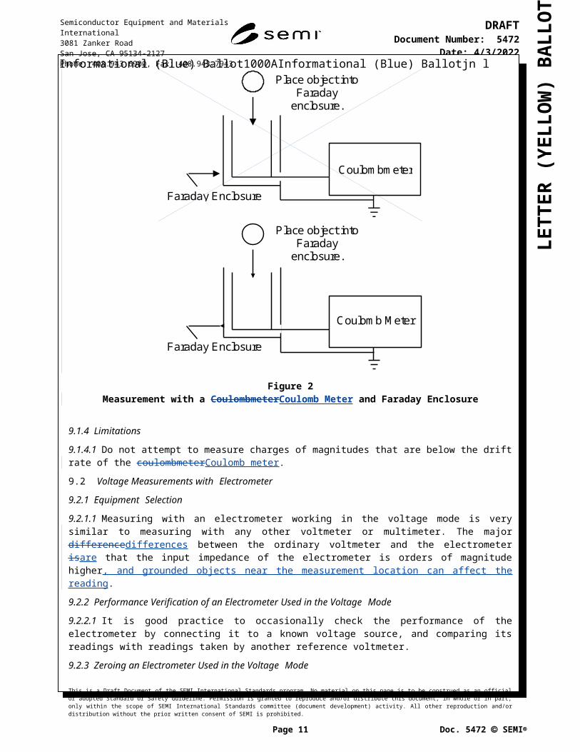
9.1.3.3 Faraday Enclosure Measurements — Refer to Figure 2. To measure the charge on an object, carefully pick up the object with an insulated tool and place the charged object into the Faraday enclosure. Special handling considerations: Be careful not to add or subtract any charge in the process of moving the charged object into the Faraday enclosure. Don’t let the charged object rub or slide against any other surface, as this may add or subtract charge from the object.
This is a Draft Document of the SEMI International Standards program. No material on this page is to be construed as an official or adopted Standard or Safety Guideline. Permission is granted to reproduce and/or distribute this document, in whole or in part, only within the scope of SEMI International Standards committee (document development) activity. All other reproduction and/or distribution without the prior written consent of SEMI is prohibited.
Page 7 Doc. 5472 SEMI
Semiconductor Equipment and Materials International3081 Zanker RoadSan Jose, CA 95134-2127Phone: 408.943.6900, Fax: 408.943.7943
DRAFTDocument Number: 5472
Date: 5/16/2023

LETT
ER (Y
ELLO
W) B
ALL
OT
Informational (Blue) Ballot1000AInformational (Blue) Ballotjn l
Coulombmeter
Place object intoFaraday
enclosure.
Faraday Enclosure
Coulomb Meter
Place object into Faraday
enclosure.
Faraday Enclosure
Figure 2Measurement with a CoulombmeterCoulomb Meter and Faraday Enclosure
9.1.4 Limitations
9.1.4.1 Do not attempt to measure charges of magnitudes that are below the drift rate of the coulombmeterCoulomb meter.
9.2 Voltage Measurements with Electrometer
9.2.1 Equipment Selection
9.2.1.1 Measuring with an electrometer working in the voltage mode is very similar to measuring with any other voltmeter or multimeter. The major differencedifferences between the ordinary voltmeter and the electrometer isare that the input impedance of the electrometer is orders of magnitude higher, and grounded objects near the measurement location can affect the reading.
9.2.2 Performance Verification of an Electrometer Used in the Voltage Mode
9.2.2.1 It is good practice to occasionally check the performance of the electrometer by connecting it to a known voltage source, and comparing its readings with readings taken by another reference voltmeter.
9.2.3 Zeroing an Electrometer Used in the Voltage Mode
9.2.3.1 Except on some older analog models, there are usually no provisions to zero an electrometer. Some electrometers with analog or digital read-outs do allow offsetting of a reading, as well as relative (i.e., delta) measurements. However, the electronic zero of the electrometer is usually set by the manufacturer, and should be part of the normal calibration. It is good practice to occasionally check the zero by shorting the input terminals together and verifying that the zero reading is within the manufacturer’s specifications.
9.2.4 Measurement
This is a Draft Document of the SEMI International Standards program. No material on this page is to be construed as an official or adopted Standard or Safety Guideline. Permission is granted to reproduce and/or distribute this document, in whole or in part, only within the scope of SEMI International Standards committee (document development) activity. All other reproduction and/or distribution without the prior written consent of SEMI is prohibited.
Page 8 Doc. 5472 SEMI
Semiconductor Equipment and Materials International3081 Zanker RoadSan Jose, CA 95134-2127Phone: 408.943.6900, Fax: 408.943.7943
DRAFTDocument Number: 5472
Date: 5/16/2023

LETT
ER (Y
ELLO
W) B
ALL
OT
Informational (Blue) Ballot1000AInformational (Blue) Ballotjn l9.2.4.1 Connect the “common”‘common’ terminal of the electrometer through a test lead to the reference plane or ground. Connect the “hot”‘hot’ or signal lead to the object or test point of interest. Some electrometer measurements will use a separate wire or shield connected to the electrical ground or a guard ring. Connect this as recommended by the manufacturer of the equipment.
9.3 Electrostatic Fieldmeter and VoltmeterESVM Measurements
9.3.1 Performance Verification of Fieldmeters and VoltmetersESVMs — Refer to Figure 3.
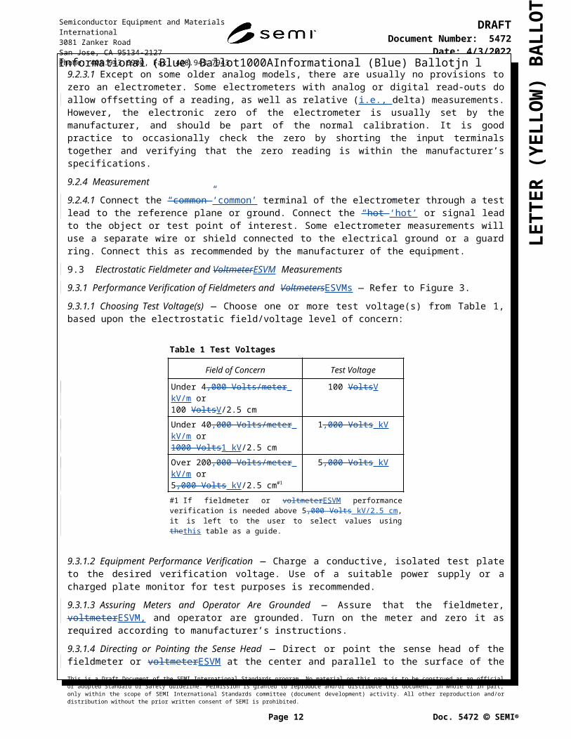
9.3.1.1 Choosing Test Voltage(s) — Choose one or more test voltage(s) from Table 1, based upon the electrostatic field/voltage level of concern:
Table 1 Test Voltages
Field of Concern Test Voltage
Under 4,000 Volts/meter kV/m or 100 VoltsV/2.5 cm
100 VoltsV
Under 40,000 Volts/meter kV/m or 1000 Volts1 kV/2.5 cm
1,000 Volts kV
Over 200,000 Volts/meter kV/m or 5,000 Volts kV/2.5 cm#1
5,000 Volts kV
#1 If fieldmeter or voltmeterESVM performance verification is needed above 5,000 Volts kV/2.5 cm, it is left to the user to select values using thethis table as a guide.
9.3.1.2 Equipment Performance Verification — Charge a conductive, isolated test plate to the desired verification voltage. Use of a suitable power supply or a charged plate monitor for test purposes is recommended.
9.3.1.3 Assuring Meters and Operator Are Grounded — Assure that the fieldmeter, voltmeterESVM, and operator are grounded. Turn on the meter and zero it as required according to manufacturer’s instructions.
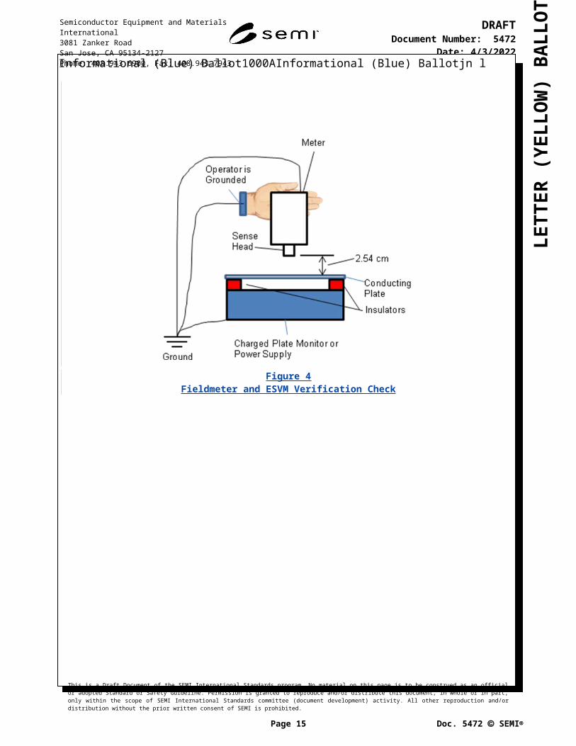
9.3.1.4 Directing or Pointing the Sense Head — Direct or point the sense head of the fieldmeter or voltmeterESVM at the center and parallel to the surface of the plate at a distance at least twice of that recommended by the manufacturer. Slowly move the sense head toward the surface of the charged plate until a reading equal to the voltage applied to the plate in ¶ 9.3.1.1 above is displayed by the meter. Measure and record the distance from the sense head to the surface to the plate. Using the plate voltage from ¶ 9.3.1.1 above and the recorded distance, compute the field strength for the fieldmeter. See Figure 3, Fieldmeter and Voltmeter Verification Check.
9.3.1.5 Alternative to ¶ 9.3.1.2 — Take measurements at a specified/fixed distance per manufacturer’s instructions. Locate the sense head of the fieldmeter or voltmeterESVM as in ¶ 9.3.1.4, but, at specified distance; reading displayed (on meter) should be within 5% of applied voltage to plate.
2: ¶ 9.3.1.4 or ¶ 9.3.1.5 should be applicable to most meters. However, in every case, the electrostatic fieldmeter or voltmeterESVM manufacturer's instructions should be read, understood, and followed.
This is a Draft Document of the SEMI International Standards program. No material on this page is to be construed as an official or adopted Standard or Safety Guideline. Permission is granted to reproduce and/or distribute this document, in whole or in part, only within the scope of SEMI International Standards committee (document development) activity. All other reproduction and/or distribution without the prior written consent of SEMI is prohibited.
Page 9 Doc. 5472 SEMI
Semiconductor Equipment and Materials International3081 Zanker RoadSan Jose, CA 95134-2127Phone: 408.943.6900, Fax: 408.943.7943
DRAFTDocument Number: 5472
Date: 5/16/2023

LETT
ER (Y
ELLO
W) B
ALL
OT
Informational (Blue) Ballot1000AInformational (Blue) Ballotjn l
Figure 3Fieldmeter and Voltmeter Verification Check
9.3.1.6 Other Desired Test Voltages — Repeat ¶ 9.3.1.4 and ¶ 9.3.1.5 for any other desired test voltages.
9.3.2 Check the zero on the fieldmeter or voltmeterESVM as specified by the manufacturer. Usually this is done while the probe is positioned to view a grounded surface. If the zero of the meter has drifted by more than 5% of the test voltage for any range contained in Table 1, the meter is not suitable for use for measurements over that range. It may be suitable for use over other ranges contained in Table 1, using other test voltages. Reverify the meter’s calibration at the selected test voltage.
9.3.3 Measurements with a Fieldmeter
9.3.3.1 Measurements made to this documentDocument should be taken/ and reported in units that conform to the customer specifications. Most common fieldmeters manufactured to date have operating instructions that reflect the user doing calibration and taking measurements in English units of VoltsV/inch or VoltsV at a fixed distance in inch(es) and in these cases, raw data are reported/listed directly. The international community specifiesand SEMI Standards program regulations specify that units shall be in SI (Standard International). System of Units (SI) units.
9.3.4 Measurement Limitations
9.3.4.1 Measurements made to this documentDocument are only valid for surfaces that are flat to a radius of 1.5 times the measurement distance from a point directly below the sensor head. For surfaces that are not flat, measurements should be made by moving the sensor over the surface such that the specified measurement distance is maintained as closely as possible. These measurements may only be stated as a range, with rounding as applicable to the meter's measurement range according to ¶ 9.3.1.1. See Figure 4, Example of a Survey of a Carrier of Semiconductor Wafers.
3: See Related Information 2 for notes on test methods environment and measurements.
This is a Draft Document of the SEMI International Standards program. No material on this page is to be construed as an official or adopted Standard or Safety Guideline. Permission is granted to reproduce and/or distribute this document, in whole or in part, only within the scope of SEMI International Standards committee (document development) activity. All other reproduction and/or distribution without the prior written consent of SEMI is prohibited.
Page 10 Doc. 5472 SEMI
Semiconductor Equipment and Materials International3081 Zanker RoadSan Jose, CA 95134-2127Phone: 408.943.6900, Fax: 408.943.7943
DRAFTDocument Number: 5472
Date: 5/16/2023
LETT
ER (Y
ELLO
W) B
ALL
OT
Informational (Blue) Ballot1000AInformational (Blue) Ballotjn l
9.3.5 Measurements with an Electrostatic Voltmeter (ESVM)
4: See Figure 3.
Figure 4Fieldmeter and ESVM Verification Check
This is a Draft Document of the SEMI International Standards program. No material on this page is to be construed as an official or adopted Standard or Safety Guideline. Permission is granted to reproduce and/or distribute this document, in whole or in part, only within the scope of SEMI International Standards committee (document development) activity. All other reproduction and/or distribution without the prior written consent of SEMI is prohibited.
Page 11 Doc. 5472 SEMI
Semiconductor Equipment and Materials International3081 Zanker RoadSan Jose, CA 95134-2127Phone: 408.943.6900, Fax: 408.943.7943
DRAFTDocument Number: 5472
Date: 5/16/2023
A) Connect meter and charged plate directly to the same ground reference.B) Hold the meter so that the sense head is approximately 2.54 cm away from the
charged plate.C) The meter reading should be within 5% of the voltage applied to the charged
plate.D) Assure that both the operator and the meter are properly grounded.
LETT
ER (Y
ELLO
W) B
ALL
OT
Informational (Blue) Ballot1000AInformational (Blue) Ballotjn l
Figure 5Example of a Survey of a Carrier of Semiconductor Wafers
9.3.6 Measurements with an Electrostatic Voltmeter
5: See Figure 3.
9.3.7 Selecting the VoltmeterESVM
9.3.7.1 Select an electrostatic voltmeterESVM with a measurement range consistent with the anticipated levels of electrostatic potentials/charge on the objects to be measured. The selection of too high a measurement range will sacrifice voltage resolution, while selection of too low a range will cause out-of-range operation (i.e., saturation).
9.3.7.2 To measure moving objects, select an electrostatic voltmeterESVM with a speed of response speed fast enough to detect the objects when they are moving past the electrostatic voltmeter probe at the highest anticipated velocity.
9.3.7.3 Select a side- or end-viewing probe for the electrostatic voltmeterESVM as is best suited to view the target object or surface when the probe is installed in an apparatusequipment.
9.3.8 Measurements
9.3.8.1 Position the probe in front of the surface to be measured. Best results are obtained when the probe is placed at the distance recommended by the manufacturer.
9.3.9 Measurement Limitations
9.3.9.1 Voltage levels on isolated conductors can be measured. Insulators do not have a uniform surface charge distribution. Therefore, it is considered that voltage levels measured on insulators indicate an electrostatic field
This is a Draft Document of the SEMI International Standards program. No material on this page is to be construed as an official or adopted Standard or Safety Guideline. Permission is granted to reproduce and/or distribute this document, in whole or in part, only within the scope of SEMI International Standards committee (document development) activity. All other reproduction and/or distribution without the prior written consent of SEMI is prohibited.
Page 12 Doc. 5472 SEMI
Semiconductor Equipment and Materials International3081 Zanker RoadSan Jose, CA 95134-2127Phone: 408.943.6900, Fax: 408.943.7943
DRAFTDocument Number: 5472
Date: 5/16/2023

LETT
ER (Y
ELLO
W) B
ALL
OT
Informational (Blue) Ballot1000AInformational (Blue) Ballotjn lstrength in a particular area. Under certain conditions, a surface charge on the insulator can be calculated from the electrostatic potential reading provided by the voltmeterESVM.
6: It is anticipated that SEMI will publishhas published an ESD Primer documentGuide (SEMI AUX021) to complement this documentDocument. Refer to the this ESD Primer documentGuide for additional information on measurements of charge on insulators.
9.4 High-Impedance Contacting Digital Voltmeter Measurements (HIDVM)
9.4.1 Equipment Selection
9.4.1.1 Measuring with an HIDVM is very similar to measuring with any other voltmeter or multimeter. The major difference between an ordinary voltmeter and the HIDVM is that the input resistance of the HIDVM is orders of magnitude higher and the input capacitance is orders of magnitude lower. This allows the HIDVM to make measurements of voltages on small objects without altering the actual voltages.
9.4.2 Performance Verification of an HIDVM
9.4.2.1 It is good practice to occasionally check the performance of the HIDVM by connecting it to a known voltage source, and comparing its readings with readings taken by another reference voltmeter.
9.4.3 Zeroing an HIDVM
9.4.3.1 Depending on the instrument used, the zero level of the HIDVM may be adjustable manually, adjustable automatically, or there may be no adjustment at all, except during the manufacturer’s normal calibration procedures. It is good practice to occasionally check the zero by shorting the input terminals together and verifying that the zero reading is within the manufacturer’s specifications. It may also be part of the normal use procedure to touch the measuring probe to a ground point to remove any residual charge before contacting the desired measurement location. Consult manufacturer’s instructions for more information.
9.4.4 Measurement
9.4.4.1 Connect the ‘common’ terminal of the HIDVM through a test lead to the reference plane or ground. Connect the measurement probe (i.e., ‘hot’ or signal lead) to the object or test point of interest. Some types of HIDVMs require the measurement probe to contact a ground point before contacting the measurement point. Particularly when measuring voltages on small objects, hold the probe as steady as possible, as changing the capacitance of the measurement system may affect the accuracy of measurement.
9.4.5 Measurement Limitations
9.4.5.1 Voltage levels on even small isolated conductors can be measured, but the HIDVM input capacitance and resistance will affect the accuracy of measurement. Prior to making measurements, a known voltage should be placed on the object of interest, and compared to the voltage measured by the HIDVM. A correction factor can thereby be developed for HIDVM measurements made on that particular object’s voltage, if necessary.
7: Refer to Related Information R1-3 for an example of a measurement procedure to determine the effect of the HIDVM probe contact on the voltage of an object.
9.5 Electrostatic Discharge Measurements
9.5.1 Principle of Operation
9.5.1.1 An ESD event generates an electromagnetic field with a specific signature characterized by:
Veryvery short rise time — as short as tens or hundreds of picoseconds, Veryvery short duration — from a few nanoseconds to several hundred nanoseconds, Veryvery broad frequency range (— up to several Gigahertz)gigahertz, and Oftenoften high magnitude.
9.5.1.2 Studies published by Intel (ESD Symposium 2005) and others provide correlationsCorrelation between the magnitude of ESD events, measurements of electromagnetic field generated by ESD events, and their magnitude. Verificationthe verification of the performance of ESD event detectors (EEDs) can also be done using the various industry ESD simulators.
8: Refer to § 12.3 for more information concerning the performance verification of EEDs.
This is a Draft Document of the SEMI International Standards program. No material on this page is to be construed as an official or adopted Standard or Safety Guideline. Permission is granted to reproduce and/or distribute this document, in whole or in part, only within the scope of SEMI International Standards committee (document development) activity. All other reproduction and/or distribution without the prior written consent of SEMI is prohibited.
Page 13 Doc. 5472 SEMI
Semiconductor Equipment and Materials International3081 Zanker RoadSan Jose, CA 95134-2127Phone: 408.943.6900, Fax: 408.943.7943
DRAFTDocument Number: 5472
Date: 5/16/2023
LETT
ER (Y
ELLO
W) B
ALL
OT
Informational (Blue) Ballot1000AInformational (Blue) Ballotjn l9.5.1.3 Such parameters as the distance between the place of discharge and the location of an antenna are a very important part of characterizing the event.
9.5.2 Measurement Equipment for ESD Events
9.5.2.1 There are several types of equipment available to detect and to measure electromagnetic fields from ESD events:.
9.5.2.2 High-Speed Storage Oscilloscopes
9.5.2.2.1 A high-speed digital storage oscilloscope equipped with proper antennaeantennas provides the most comprehensive information about waveform and magnitude of electromagnetic signals caused by ESD events. The minimum requirement for an oscilloscope used for this purpose is a 500MHz500 MHz bandwidth. Optimum bandwidth should be equal to or greater than 1GHz. The sampling rate should be at least 5five times the bandwidth.
9.5.2.2.2 Equipment with lesser performance specifications would either miss or misinterpret important parameters of ESD events.
9.5.2.2.3 The use of a high-speed oscilloscope mustshould be accompanied by the use of a proper antenna for receiving the electromagnetic fields. For time-domain measurements it is important to use an antenna with a flat frequency response since frequency correction that is common in the frequency domain is not possible for time-domain measurements. Also, it is important to note that a typical oscilloscope captures only one event ( e.g., first or last one, depending on trigger setting), missing multiple ESD events that are common.
9.5.2.2.4 Spectrum analyzers commonly used in electromagnetic compatibility (EMC) testtesting and wireless communication are not practical for detecting eletromagneticelectromagnetic signals from ESD events due to their unacceptably low acquisition speed. Refer to SEMI E33 for more information on EMC.
9.5.2.3 ESD Event MonitorsDetectors (EED)
9.5.2.3.1 While an oscilloscope provides comprehensive information on the waveform of the ESD event, it may not be practical for continuous monitoring of ESD occurrences in the process, nor in multipoint measurements due to limitations of the number of channels. ESD event monitorsEEDs provide detection and measurement ofmeasurements related to the strength of an ESD event with the ability to perform multipoint measurements and data collection at much lower cost than an oscilloscope.
9.5.2.3.2 ESD event monitorsEEDs may range from a simple device with only an indication of the occurrence of an ESD event, to a more complex device that can measure the strength of each individual ESD event and provide correlation to the strength of the electrostatic dischargeESD based on the distance from the location of the dischargeESD and other parameters.
9.5.2.3.3 More advanced ESD event monitorsEEDs can provide resolution of multiple dischargesESD events and separation between ESD events and other electromagnetic events with similar properties.
10 Certification10.1 It is reasonable to expect that the person chosen to survey production areas for staticelectrostatic charge levels has been certified to perform that task. The certified person shallshould be someone qualified by education and/or training to calibrate and make measurements with the equipment called out in this document.Document. The ESD Association conducts such education programs and certifies individuals as ESD Program Managers. 1 The International Association for Radio, Telecommunications, and Electromagnetics (iNARTE) administers an ESD Engineer and ESD technicianTechnician certification program.2
11 Documentation11.1 Meter calibration check(s), benchmark or laboratory measurements, items/areas surveys, and/or any other electrostatic field measurements should be recorded in permanent records.
11.2 Recorded are initial reading, second/validation reading, and any subsequent readings taken to verify that acceptable levels are observed. Record sheet(s) should include the meter used, area (name), location, date, environmental information if available (for example, temperature and humidity), name of person who took readings, and space for comments.
This is a Draft Document of the SEMI International Standards program. No material on this page is to be construed as an official or adopted Standard or Safety Guideline. Permission is granted to reproduce and/or distribute this document, in whole or in part, only within the scope of SEMI International Standards committee (document development) activity. All other reproduction and/or distribution without the prior written consent of SEMI is prohibited.
Page 14 Doc. 5472 SEMI
Semiconductor Equipment and Materials International3081 Zanker RoadSan Jose, CA 95134-2127Phone: 408.943.6900, Fax: 408.943.7943
DRAFTDocument Number: 5472
Date: 5/16/2023
LETT
ER (Y
ELLO
W) B
ALL
OT
Informational (Blue) Ballot1000AInformational (Blue) Ballotjn l11.3 Record sheet(s) should include the meter used, area (i.e., name), location, date, environmental information if available (i.e., temperature, humidity), name of person who took readings, and space for comments.
12 Related Documents9: These documents are for information only; in . In the case of conflict, this SEMI E43 document takesDocument should take precedence. Also, it is recommended that the user review appendices to Appendices in this documentDocument before its use. Unless otherwise indicated, all documents listed should be the latest published revision.
12.1 ESD Association Standards1Including Those Also Accredited by American National Standards Institute (ANSI)]and Joint Electron Devices Engineering Council (JEDEC)
12.1.1 ANSI/ESD STM3.1-2006 — Ionization
12.1.1.1 Test methods and procedures for evaluating and selecting air-ionization equipment and systems are provided in this standard, which establishes measurement techniques to determine ion balance and charge-neutralization time for ionizers.
12.1.2 ANSI/ESD STM4.2-2006 — ESD Protective Worksurfaces-Charge Dissipation Characteristics
12.1.2.1 This standard test method prescribes a procedure for measuring the electrostatic charge dissipation characteristics or worksurfaces used for ESD control.
12.1.3 ESD ANSI/ESD STM5.1-2007 —ANSI/ESDA/JEDEC JS-001— ANSI/ESDA/JEDEC Joint Standard for Electrostatic Discharge Sensitivity Testing-Human Body Model (HBM) Component Level
12.1.3.1 This standard test method defines procedures for testing, evaluating, and classifying the ESD sensitivity of components to the defined Human Body Modelhuman body model (HBM).
12.1.4 ANSI/ESD STM5DSTM5.2-1999 — Electrostatic Discharge Sensitivity Testing-Machine Model (MM) Component Level
12.1.4.1 This standard established a test procedure for evaluating the ESD sensitivity of components to a defined Machine Model,machine model (MM), and outlines a system whereby the sensitivity of such components may be classified.
12.1.5 ANSI/ESD STM5S5.3.1-1999 — Charged Device Model (CDM)-Component Level
12.1.5.1 This standard is a test method for evaluating active and passive components’ ESD sensitivity to a defined Charged Device Model.charged device model (CDM).
12.1.6 ANSI/ESD S20.20-2007 — Protection of Electrical and Electronic Parts, Assemblies and Equipment (Excluding Electrically Initiated Explosive Devices)
12.1.6.1 This standard specifies the requirements that must be satisfied infor designing, establishing, implementing, and maintaining ESD control programs for ESD-sensitive items susceptible to discharges equal to or greater than 100 V HBM.
12.1.7 ESD SP10.1-2007 — Automated Handling Equipment (AHE)
12.1.7.1 This document covers test methods for evaluating the ESD ground integrity of automated handling equipment as well as charge generation, and charge accumulation on devices in automated handling equipmentthe AHE.
12.1.8 ANSI/ESD S541-2003 — Packaging Materials for ESD Sensitive Items
12.1.8.1 This standard presents requirements and tests methods for selecting packaging materials to be used with ESD sensitive devices.
12.2 ESD Association Advisory Documents
12.2.1 ESD ADV1.0-2004 — Glossary of Terms
1 ESD Association, 7900 Turin Rd., Bldg. 3, Rome, NY 13440-2069; http://www.esda.org2 International Association of Radio, Telecommunications, and Electromagnetics (iNARTE), 840 Queen Street, New Bern, NC 28560; http://www.narte.org
This is a Draft Document of the SEMI International Standards program. No material on this page is to be construed as an official or adopted Standard or Safety Guideline. Permission is granted to reproduce and/or distribute this document, in whole or in part, only within the scope of SEMI International Standards committee (document development) activity. All other reproduction and/or distribution without the prior written consent of SEMI is prohibited.
Page 15 Doc. 5472 SEMI
Semiconductor Equipment and Materials International3081 Zanker RoadSan Jose, CA 95134-2127Phone: 408.943.6900, Fax: 408.943.7943
DRAFTDocument Number: 5472
Date: 5/16/2023

LETT
ER (Y
ELLO
W) B
ALL
OT
Informational (Blue) Ballot1000AInformational (Blue) Ballotjn l12.2.1.1 Definitions and explanations of various terms used in ESD Association Standardsstandards and documents are covered in this advisory. It also includes other terms commonly used in the ESD industry.
12.2.2 ESD TR20.20-2000 — ESD Handbook
12.2.2.1 The ESD Handbook is a complete guide to staticelectrostatic control in the work place. Nineteen chapters cover ESD basics, control procedures, auditing, symbols, device testing, and standards.
12.2.3 ESD ADV11.2-1995 — Triboelectric Charge Accumulation Testing
12.2.3.1 The complex phenomenon of triboelectric charging is discussed in this Advisory. It covers the theory and effects of tribocharging. It reviews procedures and problems associated with various test methods that are often used to evaluate triboelectrification characteristics.
12.3 ESD Association Symposium Proceedings
12.3.1 Proceedings of the EOS/ESD Symposium, 2005, 2012
12.3.1.1 These proceedings contain papers authored by T. Maloney of Intel that describe methods for the use and calibration of ESD event detectors (EEDs).
12.4 Other Related Documents
12.4.1 United States Military Standards2
12.4.1.1 MIL-STD-1686C — ESD Control Program for Protection of Electrical and Electronic Parts, Assemblies and Equipment (Excluding Electrically Initiated Explosive Devices)
12.4.1.1.1 This military standard establishes requirements for ESD control programs. It applies to U.S.United States military agencies, contractors, subcontractors, suppliers, and vendors. It requires the establishment, implementation, and documentation of ESD control programs for staticelectrostatic-sensitive devices, but does not mandate or preclude the use of any specific ESD control materials, products, or procedures. This standard has not been officially withdrawn although it has been supercededsuperseded by ANSI/ESD S20.20 (see ¶ 12.1.6).
12.4.1.2 MIL-HDBK-263B — ESD Control Handbook for Protection of Electrical and Electronic Parts, Assemblies and Equipment (excluding Electrically Initiated Explosive Devices)
12.4.1.2.1 This reference provides guidance, but not mandatory requirements, for the establishment and implementation of an ESD control program in accordance with the requirements of MIL-STD-1686C.
12.4.2 JEDEC Standards3
12.4.2.1 JESD625A — Requirements for Handling ESD-Sensitive Devices
12.4.2.1.1 This voluntary standard establishes minimum requirements for ESD control methods and materials designed to protect electronic devices having Human Body Modelhuman body model (HBM) sensitivities of 200 V or greater. It is intended for use by semiconductor distributors, semiconductor processing and testing facilities, and semiconductor end users.
12.4.3 EIA Standards4
12.4.3.1 EIA 541 — Packaging Material Standards for ESD Sensitive Items
12.4.3.1.1 This standard is obsolete and has been replaced by ANSI/ESD S541. Refer to ¶ 12.1.8.
12.4.3.2 EIA 583 — Packaging Material Standards for Moisture Sensitive Items
12.4.3.2.1 This standard contains information regarding packaging materials used for the protection of ESD sensitive items when moisture levels are also important.
2 Naval Publication and Forms Center, 5801 Tabor Avenue, Philadelphia PA 19120 U.S.A? Defense Supply Center Columbus, P.O. Box 3990, Columbus, OH 43216-5000, USA. http://www.dscc.dla.mil 3 JEDEC Solid State Technology Association (aka the Joint Electron Device Engineering Council), 2500 Wilson Boulevard, Arlington, VA 22201-3834, USA. Telephone: 703.907.7560; Fax: 703.907.7583; http://www.jedec.org4 EIA Electronic Industries Alliance, EIA Engineering Department, Standards Sales Office, 2001 Eye Street, NW, Washington, D.C. 20006, USA; http://www.eia.org
This is a Draft Document of the SEMI International Standards program. No material on this page is to be construed as an official or adopted Standard or Safety Guideline. Permission is granted to reproduce and/or distribute this document, in whole or in part, only within the scope of SEMI International Standards committee (document development) activity. All other reproduction and/or distribution without the prior written consent of SEMI is prohibited.
Page 16 Doc. 5472 SEMI
Semiconductor Equipment and Materials International3081 Zanker RoadSan Jose, CA 95134-2127Phone: 408.943.6900, Fax: 408.943.7943
DRAFTDocument Number: 5472
Date: 5/16/2023

LETT
ER (Y
ELLO
W) B
ALL
OT
Informational (Blue) Ballot1000AInformational (Blue) Ballotjn l12.4.4 IECInternational Electrotechnical Commission (IEC) Standards5
12.4.4.1 IEC 61000-4-2 — Electromagnetic compatibility (EMC) – Part 4-2: Testing and measurement techniques –Electrostatic discharge immunity test
12.4.4.1.1 This IEC document provides requirements and test methods for ESD transient immunity.
12.4.4.2 IEC 61340-5-1 — Electrostatics – Part 5-1: Protection of electronic devices from electrostatic phenomena – General requirements
12.4.4.2.1 This IEC (International Electrotechnical Commission) document provides guidance for establishing a static an electrostatic-charge-control program.
12.4.4.3 IEC/TR 61340-5-2 Electrostatics — Part 5-2: Protection of electronic devices from electrostatic phenomena – User Guide
12.4.4.3.1 This IEC handbook supplements the information contained in Part 5-1 above.
5 International Electrotechnical Commission, 3 rue de Varembé, Case Postale 131, CH-1211 Geneva 20, Switzerland. Telephone: 41.22.919.02.11; Fax: 41.22.919.03.00; http://www.iec.ch
This is a Draft Document of the SEMI International Standards program. No material on this page is to be construed as an official or adopted Standard or Safety Guideline. Permission is granted to reproduce and/or distribute this document, in whole or in part, only within the scope of SEMI International Standards committee (document development) activity. All other reproduction and/or distribution without the prior written consent of SEMI is prohibited.
Page 17 Doc. 5472 SEMI
Semiconductor Equipment and Materials International3081 Zanker RoadSan Jose, CA 95134-2127Phone: 408.943.6900, Fax: 408.943.7943
DRAFTDocument Number: 5472
Date: 5/16/2023

LETT
ER (Y
ELLO
W) B
ALL
OT
Informational (Blue) Ballot1000AInformational (Blue) Ballotjn lAPPENDIX 1MEASUREMENT SELECTION MATRIXNOTICE: This appendixAppendix offers information related to selecting the appropriate measurement methods from those contained in this document. The material in this appendixAppendix is an official part of SEMI E43 and was approved by full letter ballot procedures on August 29, 2008XXXXXXXXX.
A1-1 Selection of an Appropriate Electrostatic Measurement MethodA1-1.1 Tables A1-1 and A1-2 are intended to assist in the selection of appropriate equipment for making electrostatic measurements. Users should note that a variety of measurement methods is available for any given situation. Consult manufacturers of the equipment for additional information concerning its proper use and applicability.
A1-1.2 Some equipment are used for making measurements of electric charge, voltage, or field indirectly. This means that the desired property can be calculated from the measurement of another physical quantity. For example, electric charge deposited on an object can be calculated from electrostatic field or electrostatic voltage ( i.e., potential) associated with that object.
Table A1-1 Recommended Equipment Types for Electrostatic Measurements
Object and Quantity
Measured
Instrument
Object and Quantity
Measured
Coulombmeter, Coulomb Meter (direct contact
with the measurement
electrode)
CoulombmeterCoulomb Meter
with the Faraday Cup
High-Impedance Contacting
Digital Voltmeter (HIDVM)
Fieldmeter Electrostatic Voltmeter (ESVM)
Electrometer (voltage
measurement mode)
Oscilloscope EMI Detector and ESD
event meterEvent
Detector (EED)
Surface charge on large surfaces
yesYes (for conductors)
yesYes, for objects limited by the size of the Faraday Cup
yesYes, indirectly
yesYes, indirectly
yesYes, indirectly
noYes, indirectly
noNo No
Surface charge on small objects and devices (stationary measurement)
yesYes (for conductors)
yesYes Yes, indirectly
noNo (method is not accurate enough)
yesYes, indirectly
yesYes, indirectly
noNo noNo
Surface charge on device/unit in process (moving parts)
no No noNo (not with a stationary Faraday Cup)
Yes, indirectly
yesYes, indirectly, but size of the measured object and presence of stray electric fields influence accuracy
yesYes, indirectly
yesYes, indirectly
noNo noNo
This is a Draft Document of the SEMI International Standards program. No material on this page is to be construed as an official or adopted Standard or Safety Guideline. Permission is granted to reproduce and/or distribute this document, in whole or in part, only within the scope of SEMI International Standards committee (document development) activity. All other reproduction and/or distribution without the prior written consent of SEMI is prohibited.
Page 18 Doc. 5472 SEMI
Semiconductor Equipment and Materials International3081 Zanker RoadSan Jose, CA 95134-2127Phone: 408.943.6900, Fax: 408.943.7943
DRAFTDocument Number: 5472
Date: 5/16/2023
LETT
ER (Y
ELLO
W) B
ALL
OT
Informational (Blue) Ballot1000AInformational (Blue) Ballotjn lObject and Quantity
Measured
Instrument
Object and Quantity
Measured
Coulombmeter, Coulomb Meter (direct contact
with the measurement
electrode)
CoulombmeterCoulomb Meter
with the Faraday Cup
High-Impedance Contacting
Digital Voltmeter (HIDVM)
Fieldmeter Electrostatic Voltmeter (ESVM)
Electrometer (voltage
measurement mode)
Oscilloscope EMI Detector and ESD
event meterEvent
Detector (EED)
Surface charge on process equipment
yesYes (for conductors)
noNo Yes, indirectly
yesYes, indirectly, but size of the measured object and presence of stray electric fields influence accuracy
yesYes, indirectly
yesYes, indirectly
noNo noNo
Voltage measurements on isolated conductors
Yes, if object capacitance is known
Yes, if object capacitance is known
Yes Yes, but measuring distance, size of the measured object, and presence of stray electric fields influence accuracy
Yes, indirectly
Yes Yes, but input impedance will affect the accuracy of measurement
No
Table A1-2 Recommended Instruments for ESD Event Measurement
Object and Quantity
Measured
Instrument
Object and Quantity
Measured
Coulombmeter, Coulomb Meter (direct contact
with the measurement
electrode)
CoulombmeterCoulomb Meter
with the Faraday Cup
High-Impedance Contacting
Digital Voltmeter (HIDVM)
Fieldmeter Electrostatic Voltmeter
(ESVM)
Electrometer (voltage
measurement mode)
Oscilloscope EMI Detector and ESD
event meterEvent
Detector (EED)
ESD event detection and measurement in facility
noNo noNo noNo noNo noNo yesNo yesYes Yes
ESD event detection and measurement in process equipment
noNo noNo noNo noNo noNo yesNo yesYes Yes
This is a Draft Document of the SEMI International Standards program. No material on this page is to be construed as an official or adopted Standard or Safety Guideline. Permission is granted to reproduce and/or distribute this document, in whole or in part, only within the scope of SEMI International Standards committee (document development) activity. All other reproduction and/or distribution without the prior written consent of SEMI is prohibited.
Page 19 Doc. 5472 SEMI
Semiconductor Equipment and Materials International3081 Zanker RoadSan Jose, CA 95134-2127Phone: 408.943.6900, Fax: 408.943.7943
DRAFTDocument Number: 5472
Date: 5/16/2023
LETT
ER (Y
ELLO
W) B
ALL
OT
Informational (Blue) Ballot1000AInformational (Blue) Ballotjn lRELATED INFORMATION 1 NOTES ON EQUIPMENTNOTICE: This related informationRelated Information is not an official part of this standard. However, itSEMI E43-XXXX and was derived from the work of the global Metrics Technical Committee. This Related Information was approved for publication by letter ballot procedures on XXXXXXXX.
10: This Related Information contains relevant information for using the standardSEMI E43 in situations commonly encountered with semiconductor manufacturing facilities and equipment. Determination of the suitability of the material is solely the responsibility of the user.
R1-1 Use of a Charged Plate MonitorR1-1.1 A charged plate monitor is an instrument typically used to monitor the performance of air ionization equipment. Monitoring is done with an electrically isolated 15 cm × 15 cm (6 inches × 6 inches) metal plate, henceforth referred to as “‘the plate.”plate’. The instrument typically provides a means to charge the plate to a known voltage (e.g., 1000 or 5000 VoltsV of either polarity), a plate sensor to determine the voltage on the plate, and timing circuitry to determine the time required to discharge the plate to a percentage of its initial charge. For the purposes of this documentDocument, the charged plate monitor, or a separate isolated plate assembly, can be used for performance verification purposes as explained in § 9.
R1-1.2 A charged conductive plate establishes a uniform electrostatic field as long as measurements are not made close to the edges and the measurement distance is small relative to the dimensions of the plate. This specification requiresDocument recommends meters capable of making field measurements at a distance of 2.54 cm (1 inch) or less from a 15 cm (6 inch) square plate as a practical means to ensure performance verification to a known field.
R1-1.3 Charged plate monitors using 15 cm square plates with a 20 pF capacitance are commonly used to determine the performance of air ionization systems. Isolators are used to assure minimal leakage to ground. A 15 cm square plate of any metal approximately 1 mm thick and isolated from adjacent surfaces using insulative standoffs is a perfectly acceptable substitute.
R1-2 The Verification ProcedureR1-2.1 The verification procedure is intended to ensure that the meter used does not drift excessively (less than 5% in 300 s [5 minutes)]) and can repeatedly measure a known field to within 5%. When actually using the meter to do a field survey, maintaining the correct distance from the sensor head to the surface or object being measured becomes the greatest source of error. If the ability of the meter operator to maintain the correct distance is within 10%, then the total error of the measurement would be within about 12% using this calibration procedure (root mean square [RMS] of the 5% drift, 5% repeatability, and 10% distance errors).
R1-2.2 If two operators using two different meters follow the verification procedure, and they both are able to maintain the correct distance to within 10% as above, then they both would be within 12% of the true field strength when measuring the same surface or object. Taking the RMS of these errors, the two operators using two meters should be within 17% of each other.
R1-2.3 Many meters read out in VoltsV/inch., therefore 100 VoltsV/inch is about 4,000 VoltsV/m.
R1-3 Use of the High-Impedance Contacting Digital Voltmeter (HIDVM)R1-3.1 The HIDVM is used to measure the voltage resulting from the charge on conductive objects. To provide accurate measurements, both high resistance and low capacitance are required. The following is an example of a test procedure to measure IC pin voltages. This procedure will give an indication of the effect of the HIDVM on the known pin voltage. It will be possible to use this information to determine a correct factor for measurements made on similar small objects. This same procedure may be performed on any object under consideration for HIDVM measurements.
R1-3.2 Equipment Required For IC Pin Voltage Measurements
R1-3.2.1 High-Voltage DC Current-Limited Power Supply — Capable of adjustable voltage output up to 1000 V minimum. For safe operation of the power supply, refer to the manufacturer’s equipment manual. Connect a 100 MΩ resistor between the positive lead of the power supply and the device under test (DUT) being charged.
This is a Draft Document of the SEMI International Standards program. No material on this page is to be construed as an official or adopted Standard or Safety Guideline. Permission is granted to reproduce and/or distribute this document, in whole or in part, only within the scope of SEMI International Standards committee (document development) activity. All other reproduction and/or distribution without the prior written consent of SEMI is prohibited.
Page 20 Doc. 5472 SEMI
Semiconductor Equipment and Materials International3081 Zanker RoadSan Jose, CA 95134-2127Phone: 408.943.6900, Fax: 408.943.7943
DRAFTDocument Number: 5472
Date: 5/16/2023
LETT
ER (Y
ELLO
W) B
ALL
OT
Informational (Blue) Ballot1000AInformational (Blue) Ballotjn lR1-3.2.2 HIDVM — With ±1000 V full scale (minimum), ±5% accuracy, 1014 Ω minimum input resistance, and 0.1 pF maximum input capacitance.
R1-3.2.3 Ionizing Blower — Used to discharge the DUT and test fixture before every measurement. Ionizer balance should be better than ±10 V.
R1-3.2.4 Test Fixture — To hold the DUT approximately 2.54 cm (1 inch) from a ground reference plate.
R1-3.3 Test Method Details for IC Pin Voltage Measurements
R1-3.3.1 Clean the DUT with isopropyl alcohol (IPA) before testing. Handle DUT with either a clean wipe or tweezers at all times after cleaning.
R1-3.3.2 Attach the DUT to the test fixture.
R1-3.3.3 Attach the ground lead from the power supply to the ground plate of the test fixture. Connect the ground lead from the HIDVM to the same point.
R1-3.3.4 Use the ionizer to discharge the test fixture and DUT before testing at each voltage level.
R1-3.3.5 Select a voltage level on the power supply and use the positive test lead from the power supply to briefly contact several pins of the DUT.
R1-3.3.6 Immediately thereafter, use the test probe of the HIDVM to measure the voltage on the DUT pins.
R1-3.3.6.1 Hold test probe on the DUT pins only long enough to record the voltage. Remove it for 10 s, and then measure the voltage quickly again. This remeasurement will give an indication of the amount of self-discharge of the DUT. If the DUT discharges more than 10% in 10 s, clean the DUT again and make sure it is thoroughly dry before repeating the measurement.
R1-3.3.6.2 In a second test, charge the DUT pins again as in R1-3.3.5 and then hold the probe on the DUT pins for the entire 10 s, to determine how much discharge is caused by the HIDVM probe on the DUT pins.
R1-3.3.6.3 Use the data from steps R1-3.3.6.1 and R1-3.3.6.2 to determine whether a modification should be made in the HIDVM voltage readings. For example, in high humidity the self-discharge may be greater than 10% in 10 s. Alternatively, the actual input resistance and capacitance of the HIDVM probe may cause a significant drop in the measured voltage after 10 s. This change will indicate that a correction of the actual voltage measured may be needed based on the approximate measurement time.
This is a Draft Document of the SEMI International Standards program. No material on this page is to be construed as an official or adopted Standard or Safety Guideline. Permission is granted to reproduce and/or distribute this document, in whole or in part, only within the scope of SEMI International Standards committee (document development) activity. All other reproduction and/or distribution without the prior written consent of SEMI is prohibited.
Page 21 Doc. 5472 SEMI
Semiconductor Equipment and Materials International3081 Zanker RoadSan Jose, CA 95134-2127Phone: 408.943.6900, Fax: 408.943.7943
DRAFTDocument Number: 5472
Date: 5/16/2023
LETT
ER (Y
ELLO
W) B
ALL
OT
Informational (Blue) Ballot1000AInformational (Blue) Ballotjn lRELATED INFORMATION 2 NOTES ON TEST METHODSNOTICE: This related informationRelated Information is not an official part of this standard. However, itSEMI E43-XXXX and was derived from the work of the global Metrics Technical Committee. This Related Information was approved for publication by letter ballot procedures on XXXXXXXX..
11: This Related Information contains relevant information for using the standardSEMI E43 in situations commonly encountered with semiconductor manufacturing facilities and equipment. Determination of the suitability of the material is solely the responsibility of the user.
R2-1 Prior handling and environmental conditions will significantly impact the field strength to be measured. Below are a numbersome examples of these considerations:. The presence of a nearby conductive grounded surface or object will tend to reduce the measured field strength.
This phenomenaphenomenon is known as field suppression and is illustrated in Figure R2-1. Ionization of the surrounding air will tend to reduce the measured field strength by neutralizing the
staticelectrostatic charge on the surface of the object. Rubbing or contacting the surface being measured with another object or surface will tend to increase the
measured field strength depending upon the tendency of the two materials in question to tribocharge. Increasing humidity will tend to reduce the field strength to be measured because it in turn will reduce the
magnitude of the charge generated on objects and, over time, assist in the neutralization of charge on objects. Projections and sharp protrusions on the object being measured, or nearby objects, will increase the field
strength. Insulating objects may have very irregular charge distributions.
R2-2 As a result of these considerations, a statican electrostatic measurement or survey made using this standardDocument is only useful if these factors are taken into account in a realistic manner. For example: Below are some examples.
If a surface is only used in a humidity- or temperature -controlled environment, field strength measurements made under these conditions are the main ones of interest. Measurements made at different humidities or temperatures may be irrelevant.
An object may present close to zero field strength in an ionized environment, yet when contacted by another object may become highly charged. This charge may persist for a period of seconds or minutes while it is neutralized by the ionized environment. The time required to return the object to its original state may be a parameter of interest.
An object resting on a grounded metal surface may have a very low external field strength. If the object is picked up and measured, the field strength may be much higher.
Objects of irregular shape and size will give highly variable readings, depending on the position of the sensor relative to the object.
Dielectric objects may give highly variable readings, depending upon the position of the sensor relative to the charge distribution on the object.
The simple act of handling an object while performing a statican electrostatic survey can change the electrostatic charge on the object. The best results will derive from making sure that objects and surfaces are treated and handled within the bounds of their actual use.
During equipment verification, maintaining constant/steady voltage is important. If the plate of the charged plate monitor is initially charged and allowed to float, its voltage will change as the meter is moved close to it.
This is a Draft Document of the SEMI International Standards program. No material on this page is to be construed as an official or adopted Standard or Safety Guideline. Permission is granted to reproduce and/or distribute this document, in whole or in part, only within the scope of SEMI International Standards committee (document development) activity. All other reproduction and/or distribution without the prior written consent of SEMI is prohibited.
Page 22 Doc. 5472 SEMI
Semiconductor Equipment and Materials International3081 Zanker RoadSan Jose, CA 95134-2127Phone: 408.943.6900, Fax: 408.943.7943
DRAFTDocument Number: 5472
Date: 5/16/2023

LETT
ER (Y
ELLO
W) B
ALL
OT
Informational (Blue) Ballot1000AInformational (Blue) Ballotjn l
Figure R1-1Field Suppression
This is a Draft Document of the SEMI International Standards program. No material on this page is to be construed as an official or adopted Standard or Safety Guideline. Permission is granted to reproduce and/or distribute this document, in whole or in part, only within the scope of SEMI International Standards committee (document development) activity. All other reproduction and/or distribution without the prior written consent of SEMI is prohibited.
Page 23 Doc. 5472 SEMI
Semiconductor Equipment and Materials International3081 Zanker RoadSan Jose, CA 95134-2127Phone: 408.943.6900, Fax: 408.943.7943
DRAFTDocument Number: 5472
Date: 5/16/2023
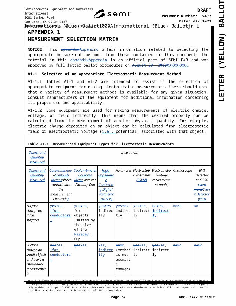
LETT
ER (Y
ELLO
W) B
ALL
OT
Informational (Blue) Ballot1000AInformational (Blue) Ballotjn lRELATED INFORMATION 3 ESD DAMAGE SIMULATORSNOTICE: This related informationRelated Information is not an official part of this standard. However, itSEMI E43-XXXX and was derived from the work of the global Metrics Technical Committee. This Related Information was approved for publication by letter ballot procedures on XXXXXXXX.
12: This Related Information contains relevant information for using the standardSEMI E43 in situations commonly encountered with semiconductor manufacturing facilities and equipment. Determination of the suitability of the material is solely the responsibility of the user.
R3-1 ESD Damage SimulatorsR3-1.1 ESD Simulatorssimulators are used to replicate ESD events. Common types used to characterize semiconductor devices and equipment include: those listed below.
Component Level-level HBM ESD Simulator Component Level-level MM ESD Simulator Component Level-level CDM ESD Simulator System Level-level HBM/metal ESD Simulator
R3-1.2 The component -level human body model (HBM (Human Body Model) ESD Simulatorsimulator represents the parameters agreed upon for a standard, which represents the discharge from a typical human body. These parameters are 1500 ohmsΩ and 100 pF for the representative resistance and capacitance respectively of the human body.
R3-1.3 The component -level machine model (MM (Machine Model) ESD Simulatorsimulator represents the parameters agreed upon for a standard, which represents the discharge from a charged metallic part of a machine (an equipment (e.g., automatic handler, etc.).). These parameters are 200 pF and zero resistance for the representative capacitance and DC resistance respectively of the machineequipment part. We note here that the resulting waveform is highly dependent on the impedance of the measurement circuitry.
R3-1.4 The component -level charged device model (CDM (Charged Device Model) ESD Simulatorsimulator represents the parameters agreed upon for a standard, which represents the discharge from a charged device. These parameters are defined by the resulting waveform and depend almost exclusively on the capacitance, resistance , and inductance of each device relative to ground. These parameters mustshould not be confused with the measuringmeasurement equipment parameters, which also affect the resulting waveform.
R3-1.5 The system-level HBM/metal ESD Simulatorsimulator represents the parameters agreed upon for a standard, which represents the discharge from a human holding a metallic instrument. These parameters are the lower resistance 350 ohmsΩ and 150 pF for the representative resistance and capacitance respectively of the human holding a metallic instrument. Note here that the waveform is greatly affected by the measuringmeasurement equipment parasitics.
1: The above component -level ESD simulators have also been used in simulating ESD damage to tooling, such as reticles. This simulation is left to user discretion.
R3-2 Summary of ProceduresR3-2.1 Component-level HBM ESD Simulator-component Level — The procedure for using this simulator to stress test devices or wafers is based upon the standard requirements. ANSI and the ESD Association approved the HBM standard, ANSI/ESD STM5.1-2007, which contains a specific device pin combination sequence for stress testing.1
This test procedure is generally referred to as a ‘Pin-to-GroundGround’ test since one pin is always grounded while the selected second pin is stressed. Calibration before use requires added equipment components like a current probe, high-bandpassband-pass cable, a short wire, a 500-ohm Ω resistor, and a very high-bandwidth waveform recorder/digitizer. A similar test method is available from JEDEC, JESD22-A114 — Electrostatic Discharge (ESD) Sensitivity Testing Human Body Model (HBM). in JESD22-A114.2
This is a Draft Document of the SEMI International Standards program. No material on this page is to be construed as an official or adopted Standard or Safety Guideline. Permission is granted to reproduce and/or distribute this document, in whole or in part, only within the scope of SEMI International Standards committee (document development) activity. All other reproduction and/or distribution without the prior written consent of SEMI is prohibited.
Page 24 Doc. 5472 SEMI
Semiconductor Equipment and Materials International3081 Zanker RoadSan Jose, CA 95134-2127Phone: 408.943.6900, Fax: 408.943.7943
DRAFTDocument Number: 5472
Date: 5/16/2023
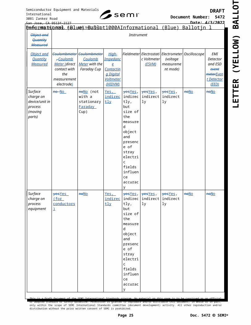
LETT
ER (Y
ELLO
W) B
ALL
OT
Informational (Blue) Ballot1000AInformational (Blue) Ballotjn lR3-2.2 Component-level MM ESD Simulator-component Level — The procedure for using this simulator to stress test devices or wafers is based upon the standard requirements. The ANSI/ESD STM5.2-1999 approved MM standard specifies a specific device pin combination sequence for stress testing.1 This test procedure is also generally referred to as a ‘Pin-to-GroundGround’ test since one pin is always grounded while the selected second pin is stressed. This procedure is exactly the same as for HBM. Calibration before use requires added equipment components like a current probe, high-bandpassband-pass cable, short wire, a 500-ohm Ω resistor, and a very high-bandwidth waveform recorder/digitizer. A similar test method is available from JEDEC, in JESD22-A115 — Electrostatic Discharge (ESD) Sensitivity Testing Machine Model (MM)..2
R3-2.3 Component-level CDM ESD Simulator-component Level — The procedure for using this simulator to stress test devices or wafers is based upon the standard requirements. The ANSI/ESD STM5.3.1-1999 approved CDM standard does not use a pin combination procedure.1 Here the device sits on a charge plate (CP) “‘dead-bug”bug’ style (i.e., package on CP and leads/pins vertical) and each pin is discharged successively after each charge to the device package. This procedure is different from that of HBM and MM. Calibration before use requires added equipment components like a capacitance/inductance calibrator, high bandpassband-pass cable, and a very high band width-bandwidth waveform recorder/digitizer. A similar test method is available from JEDEC, in JESD22-C101 — Field-Induced Charged-Device Model Test Method for Electrostatic Discharge Withstand Thresholds of Microelectronic Components.2
R3-2.4 System-level HBM-metal/Metal Simulator-system Level — The procedure for using this hand-heldhandheld simulator for testing systems (e.g., automated test equipment [ATE] testers, Automaticautomatic handlers, computers, printers, ESD Simulators, etcsimulators) is based upon the standard requirements. The IEC 61000-4-2, 1996 (formerly 801-2, 1992) standard uses direct contact or air discharge to the system under test and is a different procedure from the other three procedures mentioned above.3 Calibration before use requires the use of a very large, vertical ground plane (at least 1.2 m by 1.2 m [4 ftfoot by 4 ftfoot] square), a high bandwidth current probe, cables, and high -bandwidth waveform recorder/digitizer.
R3-3 Industry ClassificationsR3-3.1 HBM Classification
Class 0 — <250 voltsV Class 1A — 250 to <500 voltsV Class 1B — 500 to <1000 voltsV Class 1C — 1000 to <2000 voltsV Class 2 — 2000 to <4000 voltsV Class 3A — 4000 to <8000 voltsV Class 3B — ≥8000 voltsV
R3-3.2 MM Classification
Class M1 — <100 voltsV Class M2 — 100 to <200 voltsV Class M3 — 200 to <400 voltsV Class M4 — 400 to <800 voltsV Class M5 — ≥800 voltsV
R3-3.3 CDM Classification
Class C1 — <125 voltsV Class C2 — 125 to <250 voltsV Class C3 — 250 to <500 voltsV Class C4 — 500 to <1000 voltsV Class C5 —1000 to <2000 voltsV Class C6 — ≥2000 voltsV
This is a Draft Document of the SEMI International Standards program. No material on this page is to be construed as an official or adopted Standard or Safety Guideline. Permission is granted to reproduce and/or distribute this document, in whole or in part, only within the scope of SEMI International Standards committee (document development) activity. All other reproduction and/or distribution without the prior written consent of SEMI is prohibited.
Page 25 Doc. 5472 SEMI
Semiconductor Equipment and Materials International3081 Zanker RoadSan Jose, CA 95134-2127Phone: 408.943.6900, Fax: 408.943.7943
DRAFTDocument Number: 5472
Date: 5/16/2023
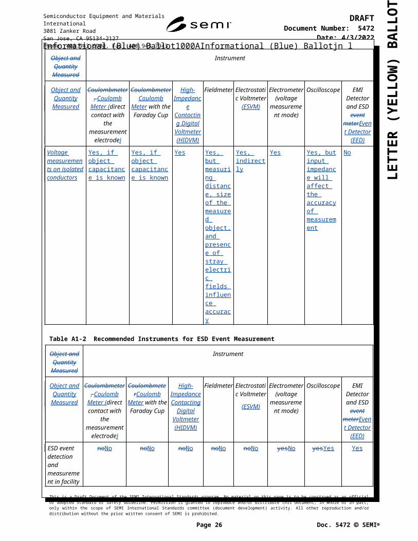
LETT
ER (Y
ELLO
W) B
ALL
OT
Informational (Blue) Ballot1000AInformational (Blue) Ballotjn lR3-3.4 Hand-HeldHandheld Metal HBM Classification
Direct Contact Discharge
Voltage Current
1. 2,000 V 12.0 AmperesA2. 4,000 V 24.0 A3. 6,000 V 36.0 A4. 8,000 V 48.0 A
Air Discharge
Voltage Current
5. 2,000 V 15.0 AmperesA6. 4,000 V 25.0 A7. 6,000 V 30.0 A8. 10,000 V 35.0 A9. 15,000 V 52.0 A
2: Note that the currents for the same voltage level are not the same for contact versus air discharge.
This is a Draft Document of the SEMI International Standards program. No material on this page is to be construed as an official or adopted Standard or Safety Guideline. Permission is granted to reproduce and/or distribute this document, in whole or in part, only within the scope of SEMI International Standards committee (document development) activity. All other reproduction and/or distribution without the prior written consent of SEMI is prohibited.
Page 26 Doc. 5472 SEMI
Semiconductor Equipment and Materials International3081 Zanker RoadSan Jose, CA 95134-2127Phone: 408.943.6900, Fax: 408.943.7943
DRAFTDocument Number: 5472
Date: 5/16/2023
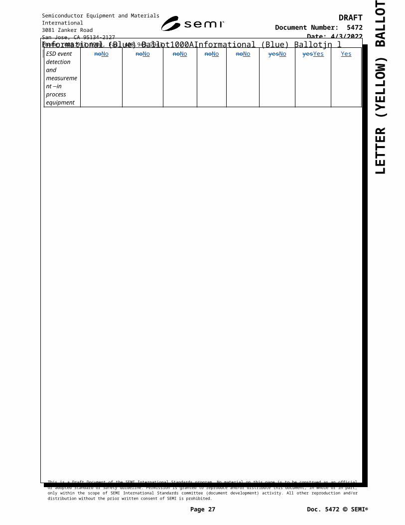
LETT
ER (Y
ELLO
W) B
ALL
OT
Informational (Blue) Ballot1000AInformational (Blue) Ballotjn lRELATED INFORMATION 4 OTHER METHODS FOR DETECTING STATICELECTROSTATIC CHARGE AND ESD EVENTS IN EQUIPMENTNOTICE: This related informationRelated Information is not an official part of this standard. However, itSEMI E43-XXXX and was derived from the work of the global Metrics Technical Committee. This Related Information was approved for publication by letter ballot procedures on XXXXXXXX.
15: This Related Information contains relevant information for using the standard in situations commonly encountered with semiconductor manufacturing facilities and equipment. Determination of the suitability of the material is solely the responsibility of the user.
R4-1 IntroductionR4-1.1 StaticElectrostatic-charge generation is unavoidable whenever materials come in contact. Without a statican electrostatic-charge-control program, the problems caused by staticelectrostatic charge are also unavoidable. The most common problem caused by staticelectrostatic charge is electrostatic discharge (ESD). ESD results in damaged semiconductor integrated circuits (ICs), photomask defects, magneto-resistive (MR) read head defects in disk drives, and failures of the drive circuits for flat panel displays (FPDFPDs). ESD also creates a significant amount of electromagnetic interference (EMI). Often mistaken for software errors, EMI resulting from ESD interrupts the operation of production equipment. This is particularly true of equipment depending on high-speed microprocessors for control. Results include unscheduled downtime, increased maintenance requirements, and frequently, product scrap. Technology trends to smaller device geometries, faster operating speeds, and increased circuit density make ESD problems worse.6
R4-1.2 For many years staticelectrostatic-charge-control programs concentrated on protecting components from the electrostatic charge generated on the personnel that handled them. Many staticelectrostatic-charge-control methods were devised to control the electrostatic charge on people including wrist and heel straps, dissipative shoes and flooring, and garments. Increasingly, however, the production of electronic components is done by automated equipment, and personnel never come into contact with the staticelectrostatic-charge-sensitive devices. Solving the ESD problem means assuring that ESD events do not occur in the equipment used to manufacture and test electronic components.
R4-2 StaticElectrostatic-Charge Control in EquipmentR4-2.1 An effective staticelectrostatic-charge-control program in equipment starts with grounding all materials that might come close to, or in contact with, the staticelectrostatic-charge-sensitive components. This prevents the generation of staticelectrostatic charge on machineequipment components and eliminates them as a source of the electrostatic-charge-creating ESD events. Care mustshould be taken in a grounding program to assure that moving equipment parts remain grounded when they are in motion. In some cases, staticelectrostatic-charge-dissipative materials may be substituted for conductive materials where flexibility, thermal insulation, or other properties not available in conductive materials are needed. If electrostatic charging of components is unavoidable, staticelectrostatic-charging-dissipative materials may be used to slow the resulting ESD discharges and prevent component damage.
R4-2.2 Most semiconductors use insulating packaging materials such as ceramics and epoxy. Handling these insulating materials inevitably generates staticelectrostatic charge, and this charge cannot be removed by grounding the materials. If electrostatic-charge generation is unavoidable, the only effective method of neutralizing the electrostatic charge on insulators or isolated conductors is to use air ionization. Ionizers are typically mounted in the load stations and process chambers of the automated equipment to neutralize the staticelectrostatic charge.
R4-3 Verifying Equipment StaticElectrostatic Charge ControlR4-3.1 A staticAn electrostatic-charge-control program begins when the automated equipment is designed by the original equipment manufacturer (OEM,), and then continues throughout the lifetime of the equipment. Two basic issues need to be demonstrated. First, are all components in the product-handling path connected to ground? Second, as the product passes through the equipment, is it handled in a way that does not generate staticelectrostatic charge 6 Levit, L. et al., “It’s the Hardware. No, Software. No, It’s ESD!”, Solid State Technology, May 1999, Pennwell Publishing Company, 98 Spit Brook Road, Nashua NH 03062.
This is a Draft Document of the SEMI International Standards program. No material on this page is to be construed as an official or adopted Standard or Safety Guideline. Permission is granted to reproduce and/or distribute this document, in whole or in part, only within the scope of SEMI International Standards committee (document development) activity. All other reproduction and/or distribution without the prior written consent of SEMI is prohibited.
Page 27 Doc. 5472 SEMI
Semiconductor Equipment and Materials International3081 Zanker RoadSan Jose, CA 95134-2127Phone: 408.943.6900, Fax: 408.943.7943
DRAFTDocument Number: 5472
Date: 5/16/2023
LETT
ER (Y
ELLO
W) B
ALL
OT
Informational (Blue) Ballot1000AInformational (Blue) Ballotjn labove an acceptable level on the component? ESD Association Standard Practice, EOS/ESD SP 10.1-20007. This document8 contains test methods to verify the integrity of the ground path to equipment parts, as well as to determine if the product is being charged during its passage through the equipment. The test methods are applicable during the original design of the equipment and during acceptance testing by the end user.
R4-3.2 While the test methods of EOS/ESD SP 10.1-2000 can also be used for periodic verification of the equipment performance, they have one drawback. The automated equipment mustshould be taken off-line to do the testing. This means that there is lost production time, and often the periodic testing is eliminated to maintain product throughput. Other test methods are available that can be performed with the equipment operating online, without altering or disturbing its operation.
R4-4 ESD and EMIR4-4.1 When ESD occurs, the discharge time is usually 10 nanosecondsns or less. Discharging energy in this short time interval results in the generation of broadband electromagnetic radiation9, as well as the heat that damages semiconductor components. This electromagnetic radiation, especially in the 10100 MHz to 2 GHz frequency range, is the electromagnetic interference (EMI) that can affect the operation of production equipment. In addition to ESD damage to semiconductor devices and reticles, ESD-caused EMI results in a variety of equipment operating problems including stoppages, software errors, testing and calibration inaccuracies, and mishandling causing physical component damage.
R4-4.2 EMI Locators — When component damage or equipment problems due to ESD are suspected, it may be useful to detect the EMI generated by the ESD event. This type of testing is both a starting point for determining that staticelectrostatic charge has been generated, and it is a measurement point to ascertain that any staticelectrostatic-charge- control methods have been successful. EMI locators measure dynamic operating conditions, as it is usually not necessary to interrupt equipment operations to make measurements.
R4-4.3 Types of EMI Locators — EMI locators are available in a number of different forms. In its simplest form, it consists of an AMamplitude modification (AM) radio tuned off station. A popping noise will be heard when an ESD event occurs. At the most complex it consists of a wideband (i.e., greater than 1 GHz) digital storage oscilloscope with a set of appropriate antennas, probes, and software. Measurements of radiated interference can be made using antennas while probes can be connected to equipment parts or electronics and power lines.
R4-4.3.1 An oscilloscope attached to a single antenna can assist in pinpointing the actual location of the ESD event.8, 10, 11, 12 A set of antennas can be used to not only detect the presence of an ESD event, but to determine the location of the pulse in 3three dimensions.13, 14 Using the same concept as a global positioning system (GPS), the difference in the arrival times of the signal to multiple antennas is directly related to the difference in the distance of each antenna from the ESD source. With the time deltas and the locations of the antennas known, the location of the spark can be uniquely identified employing the appropriate analysis program.
R4-4.3.2 Several other types of EMI -locating equipment are currently in use. Most consist of high-frequency receiving circuitry followed by level detectors to determine the magnitude of the signal. For the purpose of detecting EMI from ESD events, the equipment should have some way of differentiating the short impulse of EMI from the ESD event from the continuous high-frequency radiation of other EMI sources. Some instruments contain a counter to total the number of ESD events above the threshold, or alarms to indicate when the number of ESD events exceeds a preset number. This type of instrument can be placed near a piece ofthe equipment that is suspected of causing ESD events and left in place to monitor.7 EOS/ESD SP10.1 - 2000 “Automated Handling Equipment (AHA)”, ESD Association, 700 Turin Road, Rome NY 13440.8 EOS/ESD SP10.1 - 2000 “Automated Handling Equipment (AHA)”, ESD Association, 700 Turin Road, Rome NY 13440.9 Tonoya, Watanabe and Honda, “Impulsive EMI Effects from ESD on Raised Floor,” 1994 EOS/ESD Symposium, pp. 164-169, ESD Association.10 Takai, Kaneko and Honda, “One of the Methods of Observing ESD Around Electronic Equipments,” 1996 EOS/ESD Symposium, pp. 186-192, ESD Association.11 Greason, Bulach and Flatley, “Non-Invasive Detection and Characterization of ESD Induced Phenomena in Electronic Systems,” 1996 EOS/ESD Symposium, pp. 193-202, ESD Association.12 Smith, “A New Type of Furniture ESD and Its Implications,” 1993 EOS/ESD Symposium, pp. 3-7, ESD Association.13 Bernier, Croft, and Lowther “ESD Sources Pinpointed by Analysis of Radio Wave Emissions,” Journal of Electrostatics (44) pp. 149-157, Nov. 1998, Elsevier Science B.V., P.O. Box 211, 1000 AE Amsterdam Netherlands.14 Lin, DeChiaro and Jon, “A Robust ESD Event Locator System with Event Characterization,” 1997 EOS/ESD Symposium, pp. 88-98, ESD Association.
This is a Draft Document of the SEMI International Standards program. No material on this page is to be construed as an official or adopted Standard or Safety Guideline. Permission is granted to reproduce and/or distribute this document, in whole or in part, only within the scope of SEMI International Standards committee (document development) activity. All other reproduction and/or distribution without the prior written consent of SEMI is prohibited.
Page 28 Doc. 5472 SEMI
Semiconductor Equipment and Materials International3081 Zanker RoadSan Jose, CA 95134-2127Phone: 408.943.6900, Fax: 408.943.7943
DRAFTDocument Number: 5472
Date: 5/16/2023

LETT
ER (Y
ELLO
W) B
ALL
OT
Informational (Blue) Ballot1000AInformational (Blue) Ballotjn lR4-4.3.3 Several EMI Locatorslocators are battery-operated, handheld devices that can be easily carried around a facility or placed directly in equipment to check for ESD events. This allows the LocatorEMI locator to detect signals that might otherwise be shielded by the equipment’s cover panels. (Note that EMI shielding is usually an important part of the design of most production equipment to prevent radiation from the equipment. This makes the detection of ESD events outside the equipment more difficult.). It allows pinpointing of the location of an ESD event, which can then be correlated to particular machineequipment operations.8, 15
R4-4.4 Limitation in Using EMI Locators
R4-4.4.1 One caution needs to be observed when using EMI locators to detect ESD events that cause component damage. The signal received by these devices is generated in areas usually surrounded by grounded metal components. It may have to pass through equipment panels and travel some distance through the air before it reaches the detector. There maybe other radio-frequency (RF) sources and reflecting or absorbing materials in the area. The actual location of the ESD event may be a considerable distance from the EMI locator. It will be difficult to establish any correlation between the amplitude of the signal received by the EMI locator and the energy in the ESD event that produced the signal. The EMI locator primarily indicates the occurrence of an ESD event and can be used to illustrate that a particular staticelectrostatic-charge-control method has eliminated it. It should not be assumed that every ESD event detected results in damage to components or equipment problems. Additional testing will be needed to establish that connection.
R4-5 StaticESD Event DetectorsR4-5.1 StaticESD event detectors (SEDEED) are devices that are installed directly on products to detect the presence of an ESD event. They may be attached in proximity to an ESD-sensitive component, connected to the external device leads, or integrated into the device package. Typically they detect the current pulse of an ESD event through an antenna or direct connection to the device circuitry.
R4-5.2 SEDsEEDs can be useful in determining the occurrence of ESD events in operating production equipment. The SEDEED has the ability to indicate ESD events of a known level, aiding in the design and performance verification of automated equipment. While costly analysis of failed devices can also provide this information, correlation to machineequipment operations is usually difficult. An SEDEED that can be monitored optically as it passes through operating equipment provides a convenient method to verify that automated equipment is not generating levels of staticelectrostatic charge that result in ESD damage.
R4-6 Types of SEDEED DevicesR4-6.1 In some SEDEED devices, the signal is amplified and processed to produce a reflectance change in the built-in liquid crystal display (LCD). The SEDEED is designed to trip at a predetermined threshold voltage, detecting ESD transients above the selected amplitude. Some devices can be reset magnetically or optically making them reusable.
R4-6.2 Other devices use the controllable ESD-damage threshold of metal-oxide-semiconductor field-effect transistors (MOSFETMOSFETs). The test methodology is to amplify an ESD transient to create sufficient energy to destroy the gate oxide. The device may be used until the specified ESD level is achieved, and then the SEDEED fails. A similar device is based on the metal-oxide-semiconductor capacitor (MOSCAP). The current leakage through the device significantly increases if the ESD amplitude is sufficient to damage the MOS structure. Both of these types of SED must beEED are removed from where they are installed and require additional instrumentation to determine their status.
R4-6.3 Another type of SEDEED employs the magnetic fields from a current flow to affect a series of magneto-optic thin films. The magnetic field from the ESD current alters the film’s magnetic state and affects the degree of polarization of visible light reflected from the film. Varying the distance between the film and the ESD current-carrying conductor indicates different thresholds. This SEDEED can be read using a microscope equipped with a polarizing element and does not need to be removed from the circuitry to be read. It can be reset with a magnet.16
15 Fujie, A., “Pinpointing Sources of Static Electricity with EMI Locator,” Parts 1 and 2, Nikkei Electronics Asia, December 1992 and January 1993, Nikkei Business Publications Asia Ltd., 533 Hennessy Road, Causeway Bay, Hong Kong.16 Jackson, Tan, and Boehm, “Magneto Optical Static Event Detector,” 1998 EOS/ESD Symposium, pp.233-244, ESD Association.
This is a Draft Document of the SEMI International Standards program. No material on this page is to be construed as an official or adopted Standard or Safety Guideline. Permission is granted to reproduce and/or distribute this document, in whole or in part, only within the scope of SEMI International Standards committee (document development) activity. All other reproduction and/or distribution without the prior written consent of SEMI is prohibited.
Page 29 Doc. 5472 SEMI
Semiconductor Equipment and Materials International3081 Zanker RoadSan Jose, CA 95134-2127Phone: 408.943.6900, Fax: 408.943.7943
DRAFTDocument Number: 5472
Date: 5/16/2023
LETT
ER (Y
ELLO
W) B
ALL
OT
Informational (Blue) Ballot1000AInformational (Blue) Ballotjn lR4-7 ConclusionR4-7.1 There is little question that staticelectrostatic-charge problems continue to result in significant losses in high-technology manufacturing. Increasingly, staticelectrostatic-charge-control methods must beare applied in the equipment that produces the product. It will be important to develop and utilize a range of diagnostic methods and measurement equipment for ESD in equipment.
REVISION RECORDCHANGES IN THIS DOCUMENT FROM E43-0301NOTICE: The following information is provided to track revisions to this document. Document. Negative votes may not be cast against this information. Changes canmay be submitted to SEMIStandards Staff via a Publication Improvement Proposal (PIP) form available from the SEMI Standards Web site.
Cycle Authorization Section Description
1108 Ballot 4241 Entire Document
Complete rewrite:Title — Change of the document title from: “Guide For Measuring Static Charge On Objects And Surfaces” to “Recommended Practice for Electrostatic Measurements on Objects and Surfaces.”Purpose — Change of the purpose of the document from: “to establish a guide for reproducible measurement of electrostatic charge(s)” to “to establish a guide for reproducible electrostatic measurements.”Scope — The scope of the document was broadened by including voltage, field level(s) and electrostatic discharge measurements (¶2.1). The applicability of the standard was identified as ‘semiconductor manufacturing environments.”Limitations — Minor revisions to ¶ 3.1, 3.2 and ¶ 3.3.Terminology — Definition of “Ground” moved from ¶5.3 to ¶5.2.Safety Precautions — The title of the paragraph changed, updates to ¶¶ 6.1–6.3.Equipment — Major changes: definitions of the equipment, removed performance verification and zeroing procedures descriptions - those were moved to § 9 Test and Measurement. Table 1, Test Voltages, was also moved to § 9.Sufficient Number of Measurements — Title of the section changed from “Sampling.” The section was updated with more precise recommendations.Test Methods and Measurements — Significant updates to all paragraphs. Table 2, Measurement Units, was removed as it is no longer relevant. A new paragraph, ¶ 9.4 Electrostatic Discharge Measurements, was added.Certification — Updates to all paragraphs in this section.Documentation — Updates to ¶ 11.1. New Figure 2.Related Documents — Updates to reflect recent changes and revisions to the referenced documents.Appendix 1, Measurement Selection Matrix — Numerous changes to ¶ A1.1. Table A1-1 Measurement Method Recommendations replaced by two separate tables: Table A1-1 Recommended Instruments for Electric Charge Measurements, and Table A1-2 Recommended Instruments for ESD Event Measurements.Related Information 1, Notes on Equipment — Minor updates to all paragraphs.
0213 Ballot 5472 1.0 Title — Change of the Document title from: “Recommended Practice for Electrostatic Measurements on Objects and Surfaces.” to “Guide for Electrostatic Measurements on Objects and Surfaces”.
0213 Ballot 5472 5.1 Added new acronyms and used them throughout the Document0213 Ballot 5472 7.4, 9.4 Added information on the high-impedance contacting digital voltmeter (HIDVM)0213 Ballot 5472 12.3 Added ESD Association Symposium proceedings0213 Ballot 5472 Appendix
A1Added HIDVM to Table A1-1
This is a Draft Document of the SEMI International Standards program. No material on this page is to be construed as an official or adopted Standard or Safety Guideline. Permission is granted to reproduce and/or distribute this document, in whole or in part, only within the scope of SEMI International Standards committee (document development) activity. All other reproduction and/or distribution without the prior written consent of SEMI is prohibited.
Page 30 Doc. 5472 SEMI
Semiconductor Equipment and Materials International3081 Zanker RoadSan Jose, CA 95134-2127Phone: 408.943.6900, Fax: 408.943.7943
DRAFTDocument Number: 5472
Date: 5/16/2023

LETT
ER (Y
ELLO
W) B
ALL
OT
Informational (Blue) Ballot1000AInformational (Blue) Ballotjn lCycle Authorization Section Description
0213 Ballot 5472 Related Information R1-3
Added procedure to determine the effect of the HIDVM on the accuracy of measurements.
NOTICE: SEMI makes no warranties or representations as to the suitability of the standard(s) set forth herein for any particular application. The determination of the suitability of the standard(s) is solely the responsibility of the user. Users are cautioned to refer to manufacturer’s instructions, product labels, product data sheets, and other relevant literature respecting any materials or equipment mentioned herein. These standards are subject to change without notice.
By publication of this standard, Semiconductor Equipment and Materials International (SEMI) takes no position respecting the validity of any patent rights or copyrights asserted in connection with any item mentioned in this standard. Users of this standard are expressly advised that determination of any such patent rights or copyrights, and the risk of infringement of such rights are entirely their own responsibility.
This is a Draft Document of the SEMI International Standards program. No material on this page is to be construed as an official or adopted Standard or Safety Guideline. Permission is granted to reproduce and/or distribute this document, in whole or in part, only within the scope of SEMI International Standards committee (document development) activity. All other reproduction and/or distribution without the prior written consent of SEMI is prohibited.
Page 31 Doc. 5472 SEMI
Semiconductor Equipment and Materials International3081 Zanker RoadSan Jose, CA 95134-2127Phone: 408.943.6900, Fax: 408.943.7943
DRAFTDocument Number: 5472
Date: 5/16/2023
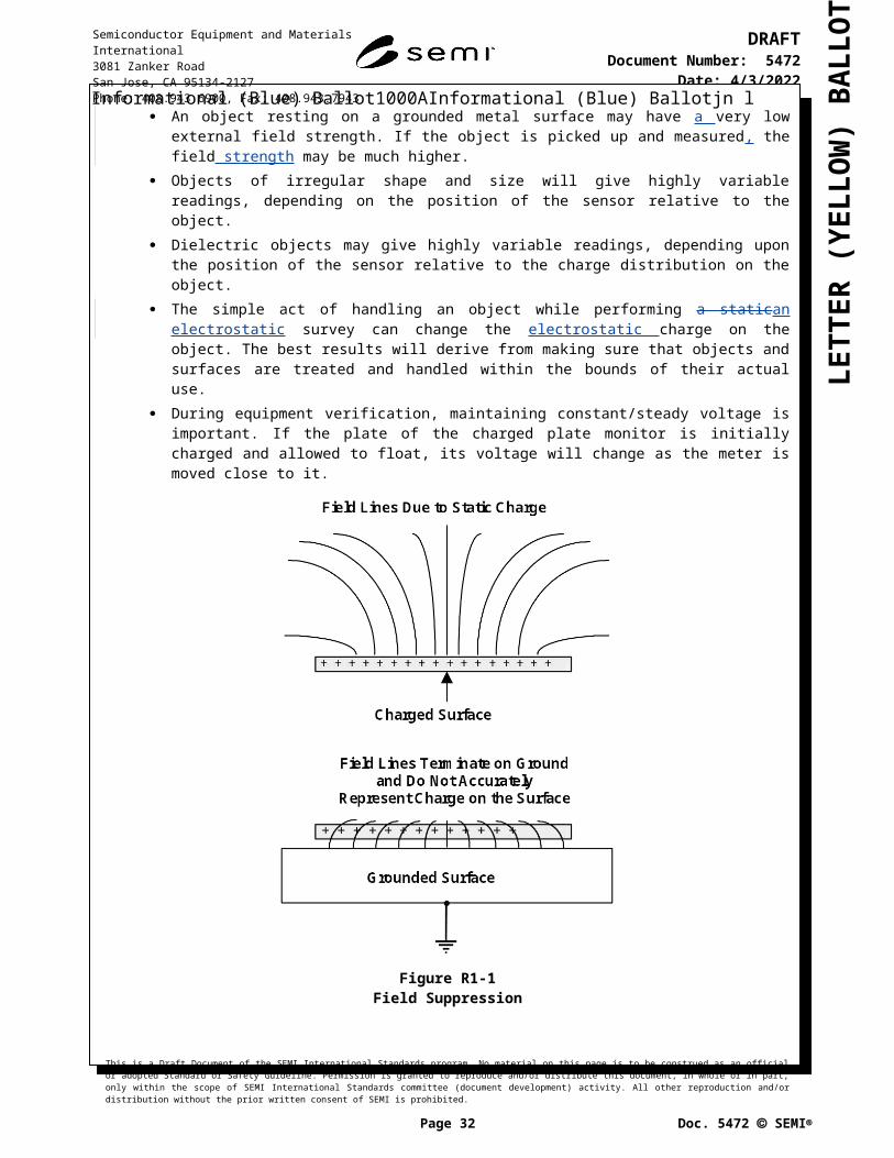
LETT
ER (Y
ELLO
W) B
ALL
OT
Informational (Blue) Ballot1000AInformational (Blue) Ballotjn lSEMI Draft Document 5472REVISION OF SEMI E43-1108,RECOMMENDED PRACTICE FOR ELECTROSTATIC MEASUREMENTS ON OBJECTS AND SURFACES with title change to: GUIDE FOR ELECTROSTATIC MEASUREMENTS ON OBJECTS AND SURFACES
1 Purpose1.1 The purpose is to provide guidance for reproducible electrostatic measurements on any surface or object, consistent with the scope and limitations set forth below.
2 Scope2.1 The measurement methods described herein can be applied to characterize the general electrostatic charge, voltage, field level(s), and electrostatic discharge (ESD) on objects and surfaces in semiconductor manufacturing environments. Acceptable equipment, calibration, and measurement techniques are described in this Document. Appendices include background information on the equipment specified and calibration procedures, as well as information and advice on performing a useful general electrostatic survey.
NOTICE: SEMI Standards and Safety Guidelines do not purport to address all safety issues associated with their use. It is the responsibility of the users of the Documents to establish appropriate safety and health practices, and determine the applicability of regulatory or other limitations prior to use.
3 Limitations3.1 Direct measurement of charge requires the use of a Coulomb meter. Charges on an isolated conductor can be measured by transferring the charge into the Coulomb meter by contacting the isolated conductor with the Coulomb meter input probe. Charges on isolated conductors and insulators can be measured by transferring the charged object into a Faraday enclosure that is connected to the Coulomb meter. These measurements can be relatively precise if care is taken in the transfer process to avoid changing the charge level when making the measurements.
3.2 Direct measurement of charge is often impractical, due to the object size or difficulties in moving the charged object from its location to the Faraday enclosure. In these instances, charge is indirectly evaluated by measurement of the electrostatic field or the electrostatic potential of a charged surface using an electrostatic fieldmeter, electrostatic voltmeter, electrometer in the voltage-measurement mode, or a high-impedance contacting digital voltmeter (HIDVM).
3.3 This Document does not describe equipment and techniques capable of making highly precise measurement of electrostatic charge. No methods of preconditioning the surface prior to measurements and no methods of character-izing the basic electrostatic performance of materials, such as tribocharging, resistance/resistivity, and decay rate are a part of this Document. Measurements made using this Document on the same surface or object may differ due to differences in the environment or history of the surface or object between the times any two measurements are made.
4 Referenced Standards and Documents4.1 SEMI Standards
SEMI E33 — Guide for Semiconductor Manufacturing Equipment Electromagnetic Compatibility (EMC)
NOTICE: Unless otherwise indicated, all documents cited shall be the latest published versions.
5 Terminology5.1 Acronyms
5.1.1 ANSI — American National Standards Institute
This is a Draft Document of the SEMI International Standards program. No material on this page is to be construed as an official or adopted Standard or Safety Guideline. Permission is granted to reproduce and/or distribute this document, in whole or in part, only within the scope of SEMI International Standards committee (document development) activity. All other reproduction and/or distribution without the prior written consent of SEMI is prohibited.
Page 32 Doc. 5472 SEMI
Semiconductor Equipment and Materials International3081 Zanker RoadSan Jose, CA 95134-2127Phone: 408.943.6900, Fax: 408.943.7943
DRAFTDocument Number: 5472
Date: 5/16/2023

LETT
ER (Y
ELLO
W) B
ALL
OT
Informational (Blue) Ballot1000AInformational (Blue) Ballotjn l5.1.2 AHE — automated handling equipment
5.1.3 CDM — charged device model
5.1.4 DC — direct current
5.1.5 EED — ESD event detector
5.1.6 EMC — electromagnetic compatibility
5.1.7 EMI — electromagnetic interference
5.1.8 ESD — electrostatic discharge
5.1.9 ESVM — electrostatic voltmeter
5.1.10 HBM — human body model
5.1.11 HIDVM — high-impedance contacting digital voltmeter
5.1.12 IC — integrated circuit
5.1.13 IEC — International Electrotechnical Commission
5.1.14 iNARTE — International Association for Radio, Telecommunications, and Electromagnetics
5.1.15 JEDEC — Joint Electron Devices Engineering Council
5.1.16 LSR — low series resistance
5.1.17 MIL-STD — United States Military Standard
5.1.18 MM — machine model
5.1.19 SI — International System of Units
5.2 Definitions
5.2.1 electromagnetic compatibility (EMC) — the ability of electronic equipment to function properly with respect to environmental electromagnetic interference (EMI). [SEMI E33]
5.2.2 electromagnetic interference (EMI) — the degradation of the performance of an equipment, transmission channel, or system caused by an electromagnetic disturbance. [SEMI E33]
5.2.3 electrostatic discharge (ESD) — the rapid spontaneous transfer of electrostatic charge induced by a high electrostatic field. [SEMI E78]
2: ESD may also be referred to as an ‘ESD event’.
5.2.4 grounded — connected to earth or some other conducting body that serves in the place of earth.
5.2.5 ground — a conducting connection between an object, electrical equipment, and earth, such as the portion of an electrical circuit of the same electrical potential as earth.
6 Safety Precautions6.1 Measurements of Very High Electrostatic Potentials (>30,000 V)
6.1.1 Measurements of very high electrostatic potentials (>30,000 V) may need to be done at larger distances than the commonly used 2.54 cm (1 inch) or less to avoid exceeding the measurement range of the meter and/or an ESD event to the meter.
6.2 Measurements on Moving Objects or Surfaces
6.2.1 Care should be taken, when attempting to read electrostatic charges on moving objects or surfaces, to maintain correct distance and avoid any contact; this is to assure ‘good’ readings with no mechanical damage or personal injury.
6.3 Measurements Using Electrostatic Voltmeters
This is a Draft Document of the SEMI International Standards program. No material on this page is to be construed as an official or adopted Standard or Safety Guideline. Permission is granted to reproduce and/or distribute this document, in whole or in part, only within the scope of SEMI International Standards committee (document development) activity. All other reproduction and/or distribution without the prior written consent of SEMI is prohibited.
Page 33 Doc. 5472 SEMI
Semiconductor Equipment and Materials International3081 Zanker RoadSan Jose, CA 95134-2127Phone: 408.943.6900, Fax: 408.943.7943
DRAFTDocument Number: 5472
Date: 5/16/2023

LETT
ER (Y
ELLO
W) B
ALL
OT
Informational (Blue) Ballot1000AInformational (Blue) Ballotjn l6.3.1 Avoid touching electrostatic voltmeter probes during operation as their surfaces may be at elevated potentials that represent a shock hazard to the operator.
7 Equipment7.1 Electrometer (Direct Measurement of Electric Charge or Voltage)
7.1.1 An electrometer is an electrical instrument for measuring electric charge, electric current, and/or electrical potential difference (i.e., voltage). Measurements of electric current with an electrometer are not discussed in this Document. An electrometer that measures electric charge only is called a Coulomb meter.
7.1.2 One of the typical features of an electrometer used in the charge or the voltage measurement mode is very high input impedance. That high impedance is needed to prevent or to minimize the transfer of electric charges between the measured object and electrometer. Ideally, the input impedance would be infinite. In practice, it is limited by intrinsic, physical material properties of insulators and by stray leakage paths between the input terminals. Low-voltage electrometers (below 200 V) have typical input resistances of 10 14 Ω or higher and accuracies better than 0.1%. In the voltmeter mode, an electrometer can resolve microvolt potentials. High-voltage electrometers (kilovolts range) usually rely on resistive voltage dividers and have typical input resistances in the 10 11
Ω range with accuracies in the 1% range. It is important to evaluate and understand the burden that the input impedance of an electrometer represents when measuring charge or voltage on charged objects.
7.2 Fieldmeter/Field Sensor
7.2.1 An electrostatic fieldmeter measures the value of the electrostatic field created by an object under test. Electrostatic fieldmeters are calibrated and recommended for use at a particular distance from the charged object. Fieldmeters are best suited for making general surveys or audits, for making measurements of surfaces at very high electric potentials (i.e., charge levels), and for making measurements when long-term stability is not important. They are not well suited for measurements of surfaces with very low charge levels or when high spatial resolution of the surface charge is needed. The fieldmeter modifies the electric field that is being measured.
7.2.1.1 The fieldmeter/electrostatic locator/field sensor will henceforth be referred to as ‘fieldmeter’. For measurements in the presence of air ionization, a chopper-stabilized fieldmeter is required. The fieldmeter is typically capable of making field measurements at a distance of 2.54 cm (1 inch) or less, from the field source to the fieldmeter sensor for this Document, as written. However, see § 10.2.4 for fieldmeters that are operated at fixed distance(s), and adjust values in this Document where applicable. The handheld fieldmeter is practical as an electrostatic locator only because precise measurements need a fixed distance between the fieldmeter sensor and the object under test.
7.3 Electrostatic Voltmeter (ESVM)
7.3.1 An ESVM measures an electric potential of an object under test. An ESVM indicates the presence and allows for calculation of the charge(s) creating the electrostatic field. Under appropriate conditions, ESVMs provide a better approximation of the charge level as compared to fieldmeters. ESVMs are relatively free of drift and more environmentally stable as compared to fieldmeters.
7.3.1.1 ESVMs exhibit a high degree of accuracy that is independent of the distance from the object under test. Thus, they are considered better suited for making more accurate and repeatable measurements as compared to fieldmeters. The probe can be located very close to a charged surface without arc-over, and, under appropriate conditions, can resolve a small spatial area on a surface.
7.4 High-Impedance Contacting Digital Voltmeter (HIDVM)
7.4.1 An HIDVM is capable of making direct contact measurements of electrical potentials on small objects under test (e.g., integrated circuit [IC] pins). An HIDVM should have both a high input resistance and low capacitance (i.e., high impedance). This is necessary to avoid removing the charge from the object under test by discharging it through the input resistance or transferring it to the capacitance of the HIDVM.
7.4.1.1 For the purpose of making voltage measurements on IC pins, or similar-sized objects, the HIDVM should have an input resistance greater than 1014 Ω and an input capacitance less than 10-2 pF. In any case, testing should be done with known voltages on the object under test to establish the effect of the measurement instrument.
7.5 Meter Stability
This is a Draft Document of the SEMI International Standards program. No material on this page is to be construed as an official or adopted Standard or Safety Guideline. Permission is granted to reproduce and/or distribute this document, in whole or in part, only within the scope of SEMI International Standards committee (document development) activity. All other reproduction and/or distribution without the prior written consent of SEMI is prohibited.
Page 34 Doc. 5472 SEMI
Semiconductor Equipment and Materials International3081 Zanker RoadSan Jose, CA 95134-2127Phone: 408.943.6900, Fax: 408.943.7943
DRAFTDocument Number: 5472
Date: 5/16/2023

LETT
ER (Y
ELLO
W) B
ALL
OT
Informational (Blue) Ballot1000AInformational (Blue) Ballotjn l7.5.1 All previously mentioned measurement instruments should be turned on and preconditioned for as long a warm-up period as recommended by the manufacturer.
1: See Related Information 1 for notes on equipment accuracy and limitations.
7.6 ESD Event Detection
7.6.1 An electrostatic discharge, also commonly referred to as an ESD event, is a source of damage to the devices and reticles. Measurements of ESD events are the only direct way of assessing the actual ESD exposure. ESD events can be measured directly or indirectly. Direct measurements are possible by inserting a current probe into the discharge path and measuring the discharge current. Such measurements, though providing the maximum accuracy, are largely limited to laboratories as it is impractical to make them in an operating factory. A practical and sensitive way of identifying ESD events is by detecting a specific electromagnetic field transient that is generated by an ESD event. Though this method is a qualitative technique that does not offer the precision of the current probe measurements, it does offer a practical way of assessing ESD exposure in situ.
8 Sufficient Number of Measurements8.1 The number of independent measurements should be determined by the user. Tests can be repeated to make them more representative of actual electrostatic charge conditions in the surveyed area. The results may vary due to environment (e.g., humidity) and workstation setup/conditions. However, any measurement that is outside of user- defined limits or different than a benchmark value should be repeated more than once after performing a zero check of the measurement equipment. This is to validate previous reading(s) and/or establish range/bounds in the case of varying results on previous reading(s).
9 Test Methods, Measurements, and Performance Verification Methods9.1 Coulomb Meter Measurements
9.1.1 Equipment Selection
9.1.1.1 Use a Coulomb meter for direct measurement of charge. A feedback-type Coulomb meter is recommended for charge measurements for the most complete transfer of charge. Shunt-type Coulomb meters do not completely transfer charge and are not as straightforward to use as feedback-type Coulomb meters. When using a Faraday enclosure, the Faraday enclosure should be large enough to hold the objects to be measured. The Faraday enclosure is used to measure charge on insulating materials as well as on conductors.
9.1.2 Performance Verification of a Coulomb Meter (or an Electrometer Used in the Charge Measurement Mode)
9.1.2.1 Refer to Figure 1.
This is a Draft Document of the SEMI International Standards program. No material on this page is to be construed as an official or adopted Standard or Safety Guideline. Permission is granted to reproduce and/or distribute this document, in whole or in part, only within the scope of SEMI International Standards committee (document development) activity. All other reproduction and/or distribution without the prior written consent of SEMI is prohibited.
Page 35 Doc. 5472 SEMI
Semiconductor Equipment and Materials International3081 Zanker RoadSan Jose, CA 95134-2127Phone: 408.943.6900, Fax: 408.943.7943
DRAFTDocument Number: 5472
Date: 5/16/2023

LETT
ER (Y
ELLO
W) B
ALL
OT
Informational (Blue) Ballot1000AInformational (Blue) Ballotjn l
Figure 6Verifying Performance of the Coulomb Meter
9.1.2.2 Reset (zero) the instrument prior to each measurement.
9.1.2.3 Maintain a reference calibration capacitor. It should be a polystyrene or polypropylene 10 nF capacitor (e.g., class C0G, low series resistance [LSR]). Measure the value of the capacitor to better than 1%. It is important to handle the reference calibration capacitor very carefully. Do not touch or hold the capacitor by its body or discharge it by touching both leads with the fingers. Hold the capacitor by one lead only. Use a clip lead connected between ground and this lead of the capacitor to maneuver the other lead of the capacitor between the ‘hot’ side of the charging source and the input terminal of the Coulomb meter.
9.1.2.4 Charge the reference calibration capacitor to 1 V with a charging source (i.e., power supply). Calculate the amount of charge on the capacitor by multiplying the voltage by the value of the capacitor. Example: 1 V × 10 nF = 10 nC of charge.
9.1.2.5 Disconnect the charging source from the capacitor.
9.1.2.6 Connect the Coulomb meter input probe to the capacitor and discharge the capacitor into the Coulomb meter. The Coulomb meter should indicate the calculated value.
9.1.3 Measurements
9.1.3.1 Best results are achieved when all surfaces surrounding the measurement area are grounded (to minimize the effects of stray fields on the measurement) and when a consistent, systematic handling method is used during the measurement process. The operator should be grounded using a grounded wrist strap.
9.1.3.2 Isolated Conductors — To measure the charge on an isolated conductor, touch the lead from the Coulomb meter to the isolated conductor.
9.1.3.3 Faraday Enclosure Measurements — Refer to Figure 2. To measure the charge on an object, carefully pick up the object with an insulated tool and place the charged object into the Faraday enclosure. Special handling considerations: Be careful not to add or subtract any charge in the process of moving the charged object into the
This is a Draft Document of the SEMI International Standards program. No material on this page is to be construed as an official or adopted Standard or Safety Guideline. Permission is granted to reproduce and/or distribute this document, in whole or in part, only within the scope of SEMI International Standards committee (document development) activity. All other reproduction and/or distribution without the prior written consent of SEMI is prohibited.
Page 36 Doc. 5472 SEMI
Semiconductor Equipment and Materials International3081 Zanker RoadSan Jose, CA 95134-2127Phone: 408.943.6900, Fax: 408.943.7943
DRAFTDocument Number: 5472
Date: 5/16/2023
LETT
ER (Y
ELLO
W) B
ALL
OT
Informational (Blue) Ballot1000AInformational (Blue) Ballotjn lFaraday enclosure. Don’t let the charged object rub or slide against any other surface, as this may add or subtract charge from the object.
Figure 7Measurement with a Coulomb Meter and Faraday Enclosure
9.1.4 Limitations
9.1.4.1 Do not attempt to measure charges of magnitudes that are below the drift rate of the Coulomb meter.
9.2 Voltage Measurements with Electrometer
9.2.1 Equipment Selection
9.2.1.1 Measuring with an electrometer working in the voltage mode is very similar to measuring with any other voltmeter or multimeter. The major differences between the ordinary voltmeter and the electrometer are that the input impedance of the electrometer is orders of magnitude higher, and grounded objects near the measurement location can affect the reading.
9.2.2 Performance Verification of an Electrometer Used in the Voltage Mode
9.2.2.1 It is good practice to occasionally check the performance of the electrometer by connecting it to a known voltage source, and comparing its readings with readings taken by another reference voltmeter.
9.2.3 Zeroing an Electrometer Used in the Voltage Mode
9.2.3.1 Except on some older analog models, there are usually no provisions to zero an electrometer. Some electrometers with analog or digital read-outs do allow offsetting of a reading, as well as relative (i.e., delta) measurements. However, the electronic zero of the electrometer is usually set by the manufacturer, and should be part of the normal calibration. It is good practice to occasionally check the zero by shorting the input terminals together and verifying that the zero reading is within the manufacturer’s specifications.
9.2.4 Measurement
9.2.4.1 Connect the ‘common’ terminal of the electrometer through a test lead to the reference plane or ground. Connect the ‘hot’ or signal lead to the object or test point of interest. Some electrometer measurements will use a separate wire or shield connected to the electrical ground or a guard ring. Connect this as recommended by the manufacturer of the equipment.
9.3 Electrostatic Fieldmeter and ESVM Measurements
9.3.1 Performance Verification of Fieldmeters and ESVMs — Refer to Figure 3.
9.3.1.1 Choosing Test Voltage(s) — Choose one or more test voltage(s) from Table 1, based upon the electrostatic field/voltage level of concern:
This is a Draft Document of the SEMI International Standards program. No material on this page is to be construed as an official or adopted Standard or Safety Guideline. Permission is granted to reproduce and/or distribute this document, in whole or in part, only within the scope of SEMI International Standards committee (document development) activity. All other reproduction and/or distribution without the prior written consent of SEMI is prohibited.
Page 37 Doc. 5472 SEMI
Semiconductor Equipment and Materials International3081 Zanker RoadSan Jose, CA 95134-2127Phone: 408.943.6900, Fax: 408.943.7943
DRAFTDocument Number: 5472
Date: 5/16/2023

LETT
ER (Y
ELLO
W) B
ALL
OT
Informational (Blue) Ballot1000AInformational (Blue) Ballotjn lTable 2 Test Voltages
Field of Concern Test Voltage
Under 4 kV/m or 100 V/2.5 cm 100 VUnder 40 kV/m or 1 kV/2.5 cm 1 kVOver 200 kV/m or 5 kV/2.5 cm#1 5 kV#2 If fieldmeter or ESVM performance verification is needed above 5 kV/2.5 cm, it is left to the user to select values using this table as a guide.
9.3.1.2 Equipment Performance Verification — Charge a conductive, isolated test plate to the desired verification voltage. Use of a suitable power supply or a charged plate monitor for test purposes is recommended.
9.3.1.3 Assuring Meters and Operator Are Grounded — Assure that the fieldmeter, ESVM, and operator are grounded. Turn on the meter and zero it as required according to manufacturer’s instructions.
9.3.1.4 Directing or Pointing the Sense Head — Direct or point the sense head of the fieldmeter or ESVM at the center and parallel to the surface of the plate at a distance at least twice of that recommended by the manufacturer. Slowly move the sense head toward the surface of the charged plate until a reading equal to the voltage applied to the plate in ¶ 9.3.1.1 above is displayed by the meter. Measure and record the distance from the sense head to the surface to the plate. Using the plate voltage from ¶ 9.3.1.1 above and the recorded distance, compute the field strength for the fieldmeter. See Figure 3.
9.3.1.5 Alternative to ¶ 9.3.1.2 — Take measurements at a specified/fixed distance per manufacturer’s instructions. Locate the sense head of the fieldmeter or ESVM as in ¶ 9.3.1.4, but, at specified distance; reading displayed (on meter) should be within 5% of applied voltage to plate.
2: ¶ 9.3.1.4 or ¶ 9.3.1.5 should be applicable to most meters. However, in every case, the electrostatic fieldmeter or ESVM manufacturer's instructions should be read, understood, and followed.
9.3.1.6 Other Desired Test Voltages — Repeat ¶ 9.3.1.4 and ¶ 9.3.1.5 for any other desired test voltages.
9.3.2 Check the zero on the fieldmeter or ESVM as specified by the manufacturer. Usually this is done while the probe is positioned to view a grounded surface. If the zero of the meter has drifted by more than 5% of the test voltage for any range contained in Table 1, the meter is not suitable for use for measurements over that range. It may be suitable for use over other ranges contained in Table 1, using other test voltages. Reverify the meter’s calibration at the selected test voltage.
9.3.3 Measurements with a Fieldmeter
9.3.3.1 Measurements made to this Document should be taken and reported in units that conform to the customer specifications. Most common fieldmeters manufactured to date have operating instructions that reflect the user doing calibration and taking measurements in English units of V/inch or V at a fixed distance in inch(es) and in these cases, raw data are reported/listed directly. The international community and SEMI Standards program regulations specify that units shall be in International System of Units (SI) units.
9.3.4 Measurement Limitations
9.3.4.1 Measurements made to this Document are only valid for surfaces that are flat to a radius of 1.5 times the measurement distance from a point directly below the sensor head. For surfaces that are not flat, measurements should be made by moving the sensor over the surface such that the specified measurement distance is maintained as closely as possible. These measurements may only be stated as a range, with rounding as applicable to the meter's measurement range according to ¶ 9.3.1.1. See Figure 4.
3: See Related Information 2 for notes on test methods environment and measurements.
9.3.5 Measurements with an Electrostatic Voltmeter (ESVM)
4: See Figure 3.
This is a Draft Document of the SEMI International Standards program. No material on this page is to be construed as an official or adopted Standard or Safety Guideline. Permission is granted to reproduce and/or distribute this document, in whole or in part, only within the scope of SEMI International Standards committee (document development) activity. All other reproduction and/or distribution without the prior written consent of SEMI is prohibited.
Page 38 Doc. 5472 SEMI
Semiconductor Equipment and Materials International3081 Zanker RoadSan Jose, CA 95134-2127Phone: 408.943.6900, Fax: 408.943.7943
DRAFTDocument Number: 5472
Date: 5/16/2023
LETT
ER (Y
ELLO
W) B
ALL
OT
Informational (Blue) Ballot1000AInformational (Blue) Ballotjn l
Figure 8Fieldmeter and ESVM Verification Check
This is a Draft Document of the SEMI International Standards program. No material on this page is to be construed as an official or adopted Standard or Safety Guideline. Permission is granted to reproduce and/or distribute this document, in whole or in part, only within the scope of SEMI International Standards committee (document development) activity. All other reproduction and/or distribution without the prior written consent of SEMI is prohibited.
Page 39 Doc. 5472 SEMI
Semiconductor Equipment and Materials International3081 Zanker RoadSan Jose, CA 95134-2127Phone: 408.943.6900, Fax: 408.943.7943
DRAFTDocument Number: 5472
Date: 5/16/2023
A) Connect meter and charged plate directly to the same ground reference.B) Hold the meter so that the sense head is approximately 2.54 cm away from the
charged plate.C) The meter reading should be within 5% of the voltage applied to the charged
plate.D) Assure that both the operator and the meter are properly grounded.
LETT
ER (Y
ELLO
W) B
ALL
OT
Informational (Blue) Ballot1000AInformational (Blue) Ballotjn l
Figure 9Example of a Survey of a Carrier of Semiconductor Wafers
9.3.6 Selecting the ESVM
9.3.6.1 Select an ESVM with a measurement range consistent with the anticipated levels of electrostatic potentials/charge on the objects to be measured. The selection of too high a measurement range will sacrifice voltage resolution, while selection of too low a range will cause out-of-range operation (i.e., saturation).
9.3.6.2 To measure moving objects, select an ESVM with a speed of response fast enough to detect the objects when they are moving past the electrostatic voltmeter probe at the highest anticipated velocity.
9.3.6.3 Select a side- or end-viewing probe for the ESVM as is best suited to view the target object or surface when the probe is installed in equipment.
9.3.7 Measurements
9.3.7.1 Position the probe in front of the surface to be measured. Best results are obtained when the probe is placed at the distance recommended by the manufacturer.
9.3.8 Measurement Limitations
9.3.8.1 Voltage levels on isolated conductors can be measured. Insulators do not have a uniform surface charge distribution. Therefore, it is considered that voltage levels measured on insulators indicate an electrostatic field strength in a particular area. Under certain conditions, a surface charge on the insulator can be calculated from the electrostatic potential reading provided by the ESVM.
This is a Draft Document of the SEMI International Standards program. No material on this page is to be construed as an official or adopted Standard or Safety Guideline. Permission is granted to reproduce and/or distribute this document, in whole or in part, only within the scope of SEMI International Standards committee (document development) activity. All other reproduction and/or distribution without the prior written consent of SEMI is prohibited.
Page 40 Doc. 5472 SEMI
Semiconductor Equipment and Materials International3081 Zanker RoadSan Jose, CA 95134-2127Phone: 408.943.6900, Fax: 408.943.7943
DRAFTDocument Number: 5472
Date: 5/16/2023
LETT
ER (Y
ELLO
W) B
ALL
OT
Informational (Blue) Ballot1000AInformational (Blue) Ballotjn l5: SEMI has published an ESD Guide (SEMI AUX021) to complement this Document. Refer to this ESD Guide for additional information on measurements of charge on insulators.
9.4 High-Impedance Contacting Digital Voltmeter Measurements (HIDVM)
9.4.1 Equipment Selection
9.4.1.1 Measuring with an HIDVM is very similar to measuring with any other voltmeter or multimeter. The major difference between an ordinary voltmeter and the HIDVM is that the input resistance of the HIDVM is orders of magnitude higher and the input capacitance is orders of magnitude lower. This allows the HIDVM to make measurements of voltages on small objects without altering the actual voltages.
9.4.2 Performance Verification of an HIDVM
9.4.2.1 It is good practice to occasionally check the performance of the HIDVM by connecting it to a known voltage source, and comparing its readings with readings taken by another reference voltmeter.
9.4.3 Zeroing an HIDVM
9.4.3.1 Depending on the instrument used, the zero level of the HIDVM may be adjustable manually, adjustable automatically, or there may be no adjustment at all, except during the manufacturer’s normal calibration procedures. It is good practice to occasionally check the zero by shorting the input terminals together and verifying that the zero reading is within the manufacturer’s specifications. It may also be part of the normal use procedure to touch the measuring probe to a ground point to remove any residual charge before contacting the desired measurement location. Consult manufacturer’s instructions for more information.
9.4.4 Measurement
9.4.4.1 Connect the ‘common’ terminal of the HIDVM through a test lead to the reference plane or ground. Connect the measurement probe (i.e., ‘hot’ or signal lead) to the object or test point of interest. Some types of HIDVMs require the measurement probe to contact a ground point before contacting the measurement point. Particularly when measuring voltages on small objects, hold the probe as steady as possible, as changing the capacitance of the measurement system may affect the accuracy of measurement.
9.4.5 Measurement Limitations
9.4.5.1 Voltage levels on even small isolated conductors can be measured, but the HIDVM input capacitance and resistance will affect the accuracy of measurement. Prior to making measurements, a known voltage should be placed on the object of interest, and compared to the voltage measured by the HIDVM. A correction factor can thereby be developed for HIDVM measurements made on that particular object’s voltage, if necessary.
6: Refer to Related Information R1-3 for an example of a measurement procedure to determine the effect of the HIDVM probe contact on the voltage of an object.
9.5 Electrostatic Discharge Measurements
9.5.1 Principle of Operation
9.5.1.1 An ESD event generates an electromagnetic field with a specific signature characterized by:
very short rise time — as short as tens or hundreds of picoseconds, very short duration — from a few nanoseconds to several hundred nanoseconds, very broad frequency range — up to several gigahertz, and often high magnitude.
9.5.1.2 Correlation between the magnitude of ESD events, measurements of electromagnetic field generated by ESD events, and the verification of the performance of ESD event detectors (EEDs) can be done using the various industry ESD simulators.
7: Refer to § 12.3 for more information concerning the performance verification of EEDs.
9.5.1.3 Such parameters as the distance between the place of discharge and the location of an antenna are a very important part of characterizing the event.
9.5.2 Measurement Equipment for ESD Events
This is a Draft Document of the SEMI International Standards program. No material on this page is to be construed as an official or adopted Standard or Safety Guideline. Permission is granted to reproduce and/or distribute this document, in whole or in part, only within the scope of SEMI International Standards committee (document development) activity. All other reproduction and/or distribution without the prior written consent of SEMI is prohibited.
Page 41 Doc. 5472 SEMI
Semiconductor Equipment and Materials International3081 Zanker RoadSan Jose, CA 95134-2127Phone: 408.943.6900, Fax: 408.943.7943
DRAFTDocument Number: 5472
Date: 5/16/2023

LETT
ER (Y
ELLO
W) B
ALL
OT
Informational (Blue) Ballot1000AInformational (Blue) Ballotjn l9.5.2.1 There are several types of equipment available to detect and to measure electromagnetic fields from ESD events.
9.5.2.2 High-Speed Storage Oscilloscopes
9.5.2.2.1 A high-speed digital storage oscilloscope equipped with proper antennas provides the most comprehensive information about waveform and magnitude of electromagnetic signals caused by ESD events. The minimum requirement for an oscilloscope used for this purpose is a 500 MHz bandwidth. Optimum bandwidth should be equal to or greater than 1GHz. The sampling rate should be at least five times the bandwidth.
9.5.2.2.2 Equipment with lesser performance specifications would either miss or misinterpret important parameters of ESD events.
9.5.2.2.3 The use of a high-speed oscilloscope should be accompanied by the use of a proper antenna for receiving the electromagnetic fields. For time-domain measurements it is important to use an antenna with a flat frequency response since frequency correction that is common in the frequency domain is not possible for time-domain measurements. Also, it is important to note that a typical oscilloscope captures only one event (e.g., first or last one, depending on trigger setting), missing multiple ESD events that are common.
9.5.2.2.4 Spectrum analyzers commonly used in electromagnetic compatibility (EMC) testing and wireless communication are not practical for detecting electromagnetic signals from ESD events due to their unacceptably low acquisition speed. Refer to SEMI E33 for more information on EMC.
9.5.2.3 ESD Event Detectors (EED)
9.5.2.3.1 While an oscilloscope provides comprehensive information on the waveform of the ESD event, it may not be practical for continuous monitoring of ESD occurrences in the process, nor in multipoint measurements due to limitations of the number of channels. EEDs provide detection and measurements related to the strength of an ESD event with the ability to perform multipoint measurements and data collection at much lower cost than an oscilloscope.
9.5.2.3.2 EEDs may range from a simple device with only an indication of the occurrence of an ESD event, to a more complex device that can measure the strength of each individual ESD event and provide correlation to the strength of the ESD based on the distance from the location of the ESD and other parameters.
9.5.2.3.3 More advanced EEDs can provide resolution of multiple ESD events and separation between ESD events and other electromagnetic events with similar properties.
10 Certification10.1 It is reasonable to expect that the person chosen to survey production areas for electrostatic charge levels has been certified to perform that task. The certified person should be someone qualified by education and/or training to calibrate and make measurements with the equipment called out in this Document. The ESD Association conducts such education programs and certifies individuals as ESD Program Managers.1 The International Association for Radio, Telecommunications, and Electromagnetics (iNARTE) administers an ESD Engineer and ESD Technician certification program.2
11 Documentation11.1 Meter calibration check(s), benchmark or laboratory measurements, items/areas surveys, and/or any other electrostatic field measurements should be recorded in permanent records.
11.2 Recorded are initial reading, second/validation reading, and any subsequent readings taken to verify that acceptable levels are observed.
11.3 Record sheet(s) should include the meter used, area (i.e., name), location, date, environmental information if available (i.e., temperature, humidity), name of person who took readings, and space for comments.
12 Related Documents8: These documents are for information only. In the case of conflict, this SEMI E43 Document should take precedence. Also, it is recommended that the user review Appendices in this Document before its use. Unless otherwise indicated, all documents listed should be the latest published revision.
This is a Draft Document of the SEMI International Standards program. No material on this page is to be construed as an official or adopted Standard or Safety Guideline. Permission is granted to reproduce and/or distribute this document, in whole or in part, only within the scope of SEMI International Standards committee (document development) activity. All other reproduction and/or distribution without the prior written consent of SEMI is prohibited.
Page 42 Doc. 5472 SEMI
Semiconductor Equipment and Materials International3081 Zanker RoadSan Jose, CA 95134-2127Phone: 408.943.6900, Fax: 408.943.7943
DRAFTDocument Number: 5472
Date: 5/16/2023

LETT
ER (Y
ELLO
W) B
ALL
OT
Informational (Blue) Ballot1000AInformational (Blue) Ballotjn l12.1 ESD Association Standards17Including Those Also Accredited by American National Standards Institute (ANSI)]and Joint Electron Devices Engineering Council (JEDEC)
12.1.1 ANSI/ESD STM3.1 — Ionization
12.1.1.1 Test methods and procedures for evaluating and selecting air-ionization equipment and systems are provided in this standard, which establishes measurement techniques to determine ion balance and charge-neutralization time for ionizers.
12.1.2 ANSI/ESD STM4.2 — ESD Protective Worksurfaces-Charge Dissipation Characteristics
12.1.2.1 This standard test method prescribes a procedure for measuring the electrostatic charge dissipation characteristics or worksurfaces used for ESD control.
12.1.3 ANSI/ESDA/JEDEC JS-001— ANSI/ESDA/JEDEC Joint Standard for Electrostatic Discharge Sensitivity Testing-Human Body Model (HBM) Component Level
12.1.3.1 This standard test method defines procedures for testing, evaluating, and classifying the ESD sensitivity of components to the defined human body model (HBM).
12.1.4 ESD DSTM5.2 — Electrostatic Discharge Sensitivity Testing-Machine Model (MM) Component Level
12.1.4.1 This standard established a test procedure for evaluating the ESD sensitivity of components to a defined machine model (MM), and outlines a system whereby the sensitivity of such components may be classified.
12.1.5 ANSI/ESD S5.3.1 — Charged Device Model (CDM)-Component Level
12.1.5.1 This standard is a test method for evaluating active and passive components’ ESD sensitivity to a defined charged device model (CDM).
12.1.6 ANSI/ESD S20.20 — Protection of Electrical and Electronic Parts, Assemblies and Equipment (Excluding Electrically Initiated Explosive Devices)
12.1.6.1 This standard specifies the requirements for designing, establishing, implementing, and maintaining ESD control programs for ESD-sensitive items susceptible to discharges equal to or greater than 100 V HBM.
12.1.7 ESD SP10.1 — Automated Handling Equipment (AHE)
12.1.7.1 This document covers test methods for evaluating the ESD ground integrity of automated handling equipment as well as charge generation and charge accumulation on devices in the AHE.
12.1.8 ANSI/ESD S541 — Packaging Materials for ESD Sensitive Items
12.1.8.1 This standard presents requirements and tests methods for selecting packaging materials to be used with ESD sensitive devices.
12.2 ESD Association Advisory Documents
12.2.1 ESD ADV1.0 — Glossary of Terms
12.2.1.1 Definitions and explanations of various terms used in ESD Association standards and documents are covered in this advisory. It also includes other terms commonly used in the ESD industry.
12.2.2 ESD TR20.20 — ESD Handbook
12.2.2.1 The ESD Handbook is a complete guide to electrostatic control in the work place. Nineteen chapters cover ESD basics, control procedures, auditing, symbols, device testing, and standards.
12.2.3 ESD ADV11.2 — Triboelectric Charge Accumulation Testing
12.2.3.1 The complex phenomenon of triboelectric charging is discussed in this Advisory. It covers the theory and effects of tribocharging. It reviews procedures and problems associated with various test methods that are often used to evaluate triboelectrification characteristics.
17 ESD Association, 7900 Turin Rd., Bldg. 3, Rome, NY 13440-2069; http://www.esda.org2 International Association of Radio, Telecommunications, and Electromagnetics (iNARTE), 840 Queen Street, New Bern, NC 28560; http://www.narte.org
This is a Draft Document of the SEMI International Standards program. No material on this page is to be construed as an official or adopted Standard or Safety Guideline. Permission is granted to reproduce and/or distribute this document, in whole or in part, only within the scope of SEMI International Standards committee (document development) activity. All other reproduction and/or distribution without the prior written consent of SEMI is prohibited.
Page 43 Doc. 5472 SEMI
Semiconductor Equipment and Materials International3081 Zanker RoadSan Jose, CA 95134-2127Phone: 408.943.6900, Fax: 408.943.7943
DRAFTDocument Number: 5472
Date: 5/16/2023

LETT
ER (Y
ELLO
W) B
ALL
OT
Informational (Blue) Ballot1000AInformational (Blue) Ballotjn l12.3 ESD Association Symposium Proceedings
12.3.1 Proceedings of the EOS/ESD Symposium, 2005, 2012
12.3.1.1 These proceedings contain papers authored by T. Maloney of Intel that describe methods for the use and calibration of ESD event detectors (EEDs).
12.4 Other Related Documents
12.4.1 United States Military Standards18
12.4.1.1 MIL-STD-1686C — ESD Control Program for Protection of Electrical and Electronic Parts, Assemblies and Equipment (Excluding Electrically Initiated Explosive Devices)
12.4.1.1.1 This military standard establishes requirements for ESD control programs. It applies to United States military agencies, contractors, subcontractors, suppliers, and vendors. It requires the establishment, implementation, and documentation of ESD control programs for electrostatic-sensitive devices, but does not mandate or preclude the use of any specific ESD control materials, products, or procedures. This standard has not been officially withdrawn although it has been superseded by ANSI/ESD S20.20 (see ¶ 12.1.6).
12.4.1.2 MIL-HDBK-263B — ESD Control Handbook for Protection of Electrical and Electronic Parts, Assemblies and Equipment (excluding Electrically Initiated Explosive Devices)
12.4.1.2.1 This reference provides guidance, but not mandatory requirements, for the establishment and implementation of an ESD control program in accordance with the requirements of MIL-STD-1686C.
12.4.2 JEDEC Standards19
12.4.2.1 JESD625A — Requirements for Handling ESD-Sensitive Devices
12.4.2.1.1 This voluntary standard establishes minimum requirements for ESD control methods and materials designed to protect electronic devices having human body model (HBM) sensitivities of 200 V or greater. It is intended for use by semiconductor distributors, semiconductor processing and testing facilities, and semiconductor end users.
12.4.3 International Electrotechnical Commission (IEC) Standards20
12.4.3.1 IEC 61000-4-2 — Electromagnetic compatibility (EMC) – Part 4-2: Testing and measurement techniques –Electrostatic discharge immunity test
12.4.3.1.1 This IEC document provides requirements and test methods for ESD transient immunity.
12.4.3.2 IEC 61340-5-1 — Electrostatics – Part 5-1: Protection of electronic devices from electrostatic phenomena – General requirements
12.4.3.2.1 This IEC (International Electrotechnical Commission) document provides guidance for establishing an electrostatic-charge-control program.
12.4.3.3 IEC/TR 61340-5-2 Electrostatics — Part 5-2: Protection of electronic devices from electrostatic phenomena – User Guide
12.4.3.3.1 This IEC handbook supplements the information contained in Part 5-1 above.
18 Defense Supply Center Columbus, P.O. Box 3990, Columbus, OH 43216-5000, USA. http://www.dscc.dla.mil 19 JEDEC Solid State Technology Association (aka the Joint Electron Device Engineering Council), 2500 Wilson Boulevard, Arlington, VA 22201-3834, USA. Telephone: 703.907.7560; Fax: 703.907.7583; http://www.jedec.org20 International Electrotechnical Commission, 3 rue de Varembé, Case Postale 131, CH-1211 Geneva 20, Switzerland. Telephone: 41.22.919.02.11; Fax: 41.22.919.03.00; http://www.iec.ch
This is a Draft Document of the SEMI International Standards program. No material on this page is to be construed as an official or adopted Standard or Safety Guideline. Permission is granted to reproduce and/or distribute this document, in whole or in part, only within the scope of SEMI International Standards committee (document development) activity. All other reproduction and/or distribution without the prior written consent of SEMI is prohibited.
Page 44 Doc. 5472 SEMI
Semiconductor Equipment and Materials International3081 Zanker RoadSan Jose, CA 95134-2127Phone: 408.943.6900, Fax: 408.943.7943
DRAFTDocument Number: 5472
Date: 5/16/2023

LETT
ER (Y
ELLO
W) B
ALL
OT
Informational (Blue) Ballot1000AInformational (Blue) Ballotjn lAPPENDIX 1MEASUREMENT SELECTION MATRIXNOTICE: This Appendix offers information related to selecting the appropriate measurement methods from those contained in this document. The material in this Appendix is an official part of SEMI E43 and was approved by full letter ballot procedures on XXXXXXXXX.
A1-1 Selection of an Appropriate Electrostatic Measurement MethodA1-1.1 Tables A1-1 and A1-2 are intended to assist in the selection of appropriate equipment for making electrostatic measurements. Users should note that a variety of measurement methods is available for any given situation. Consult manufacturers of the equipment for additional information concerning its proper use and applicability.
A1-1.2 Some equipment are used for making measurements of electric charge, voltage, or field indirectly. This means that the desired property can be calculated from the measurement of another physical quantity. For example, electric charge deposited on an object can be calculated from electrostatic field or electrostatic voltage (i.e., potential) associated with that object.
Table A1-1 Recommended Equipment Types for Electrostatic Measurements
Instrument
Object and Quantity
Measured
Coulomb Meter (direct contact
with the measurement
electrode)
Coulomb Meter with the
Faraday Cup
High-Impedance Contacting
Digital Voltmeter (HIDVM)
Fieldmeter Electrostatic Voltmeter (ESVM)
Electrometer (voltage
measurement mode)
Oscilloscope EMI Detector and ESD
Event Detector (EED)
Surface charge on large surfaces
Yes (for conductors)
Yes, for objects limited by the size of the Faraday Cup
Yes, indirectly
Yes, indirectly
Yes, indirectly
Yes, indirectly
No No
Surface charge on small objects and devices (stationary measurement)
Yes (for conductors)
Yes Yes, indirectly
No (method is not accurate enough)
Yes, indirectly
Yes, indirectly
No No
Surface charge on device/unit in process (moving parts)
No No (not with a stationary Faraday Cup)
Yes, indirectly
Yes, indirectly, but size of the measured object and presence of stray electric fields influence accuracy
Yes, indirectly
Yes, indirectly
No No
This is a Draft Document of the SEMI International Standards program. No material on this page is to be construed as an official or adopted Standard or Safety Guideline. Permission is granted to reproduce and/or distribute this document, in whole or in part, only within the scope of SEMI International Standards committee (document development) activity. All other reproduction and/or distribution without the prior written consent of SEMI is prohibited.
Page 45 Doc. 5472 SEMI
Semiconductor Equipment and Materials International3081 Zanker RoadSan Jose, CA 95134-2127Phone: 408.943.6900, Fax: 408.943.7943
DRAFTDocument Number: 5472
Date: 5/16/2023
LETT
ER (Y
ELLO
W) B
ALL
OT
Informational (Blue) Ballot1000AInformational (Blue) Ballotjn lInstrument
Object and Quantity
Measured
Coulomb Meter (direct contact
with the measurement
electrode)
Coulomb Meter with the
Faraday Cup
High-Impedance Contacting
Digital Voltmeter (HIDVM)
Fieldmeter Electrostatic Voltmeter (ESVM)
Electrometer (voltage
measurement mode)
Oscilloscope EMI Detector and ESD
Event Detector (EED)
Surface charge on process equipment
Yes (for conductors)
No Yes, indirectly
Yes, indirectly, but size of the measured object and presence of stray electric fields influence accuracy
Yes, indirectly
Yes, indirectly
No No
Voltage measurements on isolated conductors
Yes, if object capacitance is known
Yes, if object capacitance is known
Yes Yes, but measuring distance, size of the measured object, and presence of stray electric fields influence accuracy
Yes, indirectly
Yes Yes, but input impedance will affect the accuracy of measurement
No
Table A1-2 Recommended Instruments for ESD Event Measurement
Instrument
Object and Quantity
Measured
Coulomb Meter (direct contact
with the measurement
electrode)
Coulomb Meter with the
Faraday Cup
High-Impedance Contacting
Digital Voltmeter (HIDVM)
Fieldmeter Electrostatic Voltmeter
(ESVM)
Electrometer (voltage
measurement mode)
Oscilloscope EMI Detector and ESD
Event Detector (EED)
ESD event detection and measurement in facility
No No No No No No Yes Yes
ESD event detection and measurement in process equipment
No No No No No No Yes Yes
This is a Draft Document of the SEMI International Standards program. No material on this page is to be construed as an official or adopted Standard or Safety Guideline. Permission is granted to reproduce and/or distribute this document, in whole or in part, only within the scope of SEMI International Standards committee (document development) activity. All other reproduction and/or distribution without the prior written consent of SEMI is prohibited.
Page 46 Doc. 5472 SEMI
Semiconductor Equipment and Materials International3081 Zanker RoadSan Jose, CA 95134-2127Phone: 408.943.6900, Fax: 408.943.7943
DRAFTDocument Number: 5472
Date: 5/16/2023

LETT
ER (Y
ELLO
W) B
ALL
OT
Informational (Blue) Ballot1000AInformational (Blue) Ballotjn lRELATED INFORMATION 1 NOTES ON EQUIPMENTNOTICE: This Related Information is not an official part of SEMI E43-XXXX and was derived from the work of the global Metrics Technical Committee. This Related Information was approved for publication by letter ballot procedures on XXXXXXXX.
11: This Related Information contains relevant information for using SEMI E43 in situations commonly encountered with semiconductor manufacturing facilities and equipment. Determination of the suitability of the material is solely the responsibility of the user.
R1-1 Use of a Charged Plate MonitorR1-1.1 A charged plate monitor is an instrument typically used to monitor the performance of air ionization equipment. Monitoring is done with an electrically isolated 15 cm × 15 cm (6 inches × 6 inches) metal plate, henceforth referred to as ‘the plate’. The instrument typically provides a means to charge the plate to a known voltage (e.g., 1000 or 5000 V of either polarity), a plate sensor to determine the voltage on the plate, and timing circuitry to determine the time required to discharge the plate to a percentage of its initial charge. For the purposes of this Document, the charged plate monitor, or a separate isolated plate assembly, can be used for performance verification purposes as explained in § 9.
R1-1.2 A charged conductive plate establishes a uniform electrostatic field as long as measurements are not made close to the edges and the measurement distance is small relative to the dimensions of the plate. This Document recommends meters capable of making field measurements at a distance of 2.54 cm (1 inch) or less from a 15 cm (6 inch) square plate as a practical means to ensure performance verification to a known field.
R1-1.3 Charged plate monitors using 15 cm square plates with a 20 pF capacitance are commonly used to determine the performance of air ionization systems. Isolators are used to assure minimal leakage to ground. A 15 cm square plate of any metal approximately 1 mm thick and isolated from adjacent surfaces using insulative standoffs is a perfectly acceptable substitute.
R1-2 The Verification ProcedureR1-2.1 The verification procedure is intended to ensure that the meter used does not drift excessively (less than 5% in 300 s [5 minutes]) and can repeatedly measure a known field to within 5%. When actually using the meter to do a field survey, maintaining the correct distance from the sensor head to the surface or object being measured becomes the greatest source of error. If the ability of the meter operator to maintain the correct distance is within 10%, then the total error of the measurement would be within about 12% using this calibration procedure (root mean square [RMS] of the 5% drift, 5% repeatability, and 10% distance errors).
R1-2.2 If two operators using two different meters follow the verification procedure, and they both are able to maintain the correct distance to within 10% as above, then they both would be within 12% of the true field strength when measuring the same surface or object. Taking the RMS of these errors, the two operators using two meters should be within 17% of each other.
R1-2.3 Many meters read out in V/inch, therefore 100 V/inch is about 4,000 V/m.
R1-3 Use of the High-Impedance Contacting Digital Voltmeter (HIDVM)R1-3.1 The HIDVM is used to measure the voltage resulting from the charge on conductive objects. To provide accurate measurements, both high resistance and low capacitance are required. The following is an example of a test procedure to measure IC pin voltages. This procedure will give an indication of the effect of the HIDVM on the known pin voltage. It will be possible to use this information to determine a correct factor for measurements made on similar small objects. This same procedure may be performed on any object under consideration for HIDVM measurements.
R1-3.2 Equipment Required For IC Pin Voltage Measurements
R1-3.2.1 High-Voltage DC Current-Limited Power Supply — Capable of adjustable voltage output up to 1000 V minimum. For safe operation of the power supply, refer to the manufacturer’s equipment manual. Connect a 100 MΩ resistor between the positive lead of the power supply and the device under test (DUT) being charged.
This is a Draft Document of the SEMI International Standards program. No material on this page is to be construed as an official or adopted Standard or Safety Guideline. Permission is granted to reproduce and/or distribute this document, in whole or in part, only within the scope of SEMI International Standards committee (document development) activity. All other reproduction and/or distribution without the prior written consent of SEMI is prohibited.
Page 47 Doc. 5472 SEMI
Semiconductor Equipment and Materials International3081 Zanker RoadSan Jose, CA 95134-2127Phone: 408.943.6900, Fax: 408.943.7943
DRAFTDocument Number: 5472
Date: 5/16/2023
LETT
ER (Y
ELLO
W) B
ALL
OT
Informational (Blue) Ballot1000AInformational (Blue) Ballotjn lR1-3.2.2 HIDVM — With ±1000 V full scale (minimum), ±5% accuracy, 1014 Ω minimum input resistance, and 0.1 pF maximum input capacitance.
R1-3.2.3 Ionizing Blower — Used to discharge the DUT and test fixture before every measurement. Ionizer balance should be better than ±10 V.
R1-3.2.4 Test Fixture — To hold the DUT approximately 2.54 cm (1 inch) from a ground reference plate.
R1-3.3 Test Method Details for IC Pin Voltage Measurements
R1-3.3.1 Clean the DUT with isopropyl alcohol (IPA) before testing. Handle DUT with either a clean wipe or tweezers at all times after cleaning.
R1-3.3.2 Attach the DUT to the test fixture.
R1-3.3.3 Attach the ground lead from the power supply to the ground plate of the test fixture. Connect the ground lead from the HIDVM to the same point.
R1-3.3.4 Use the ionizer to discharge the test fixture and DUT before testing at each voltage level.
R1-3.3.5 Select a voltage level on the power supply and use the positive test lead from the power supply to briefly contact several pins of the DUT.
R1-3.3.6 Immediately thereafter, use the test probe of the HIDVM to measure the voltage on the DUT pins.
R1-3.3.6.1 Hold test probe on the DUT pins only long enough to record the voltage. Remove it for 10 s, and then measure the voltage quickly again. This remeasurement will give an indication of the amount of self-discharge of the DUT. If the DUT discharges more than 10% in 10 s, clean the DUT again and make sure it is thoroughly dry before repeating the measurement.
R1-3.3.6.2 In a second test, charge the DUT pins again as in R1-3.3.5 and then hold the probe on the DUT pins for the entire 10 s, to determine how much discharge is caused by the HIDVM probe on the DUT pins.
R1-3.3.6.3 Use the data from steps R1-3.3.6.1 and R1-3.3.6.2 to determine whether a modification should be made in the HIDVM voltage readings. For example, in high humidity the self-discharge may be greater than 10% in 10 s. Alternatively, the actual input resistance and capacitance of the HIDVM probe may cause a significant drop in the measured voltage after 10 s. This change will indicate that a correction of the actual voltage measured may be needed based on the approximate measurement time.
This is a Draft Document of the SEMI International Standards program. No material on this page is to be construed as an official or adopted Standard or Safety Guideline. Permission is granted to reproduce and/or distribute this document, in whole or in part, only within the scope of SEMI International Standards committee (document development) activity. All other reproduction and/or distribution without the prior written consent of SEMI is prohibited.
Page 48 Doc. 5472 SEMI
Semiconductor Equipment and Materials International3081 Zanker RoadSan Jose, CA 95134-2127Phone: 408.943.6900, Fax: 408.943.7943
DRAFTDocument Number: 5472
Date: 5/16/2023

LETT
ER (Y
ELLO
W) B
ALL
OT
Informational (Blue) Ballot1000AInformational (Blue) Ballotjn lRELATED INFORMATION 2 NOTES ON TEST METHODSNOTICE: This Related Information is not an official part of SEMI E43-XXXX and was derived from the work of the global Metrics Technical Committee. This Related Information was approved for publication by letter ballot procedures on XXXXXXXX..
12: This Related Information contains relevant information for using SEMI E43 in situations commonly encountered with semiconductor manufacturing facilities and equipment. Determination of the suitability of the material is solely the responsibility of the user.
R2-1 Prior handling and environmental conditions will significantly impact the field strength to be measured. Below are some examples of these considerations. The presence of a nearby conductive grounded surface or object will tend to reduce the measured field strength.
This phenomenon is known as field suppression and is illustrated in Figure R2-1. Ionization of the surrounding air will tend to reduce the measured field strength by neutralizing the electrostatic
charge on the surface of the object. Rubbing or contacting the surface being measured with another object or surface will tend to increase the
measured field strength depending upon the tendency of the two materials in question to tribocharge. Increasing humidity will tend to reduce the field strength to be measured because it in turn will reduce the
magnitude of the charge generated on objects and, over time, assist in the neutralization of charge on objects. Projections and sharp protrusions on the object being measured, or nearby objects, will increase the field
strength. Insulating objects may have very irregular charge distributions.
R2-2 As a result of these considerations, an electrostatic measurement or survey made using this Document is only useful if these factors are taken into account in a realistic manner. Below are some examples. If a surface is only used in a humidity- or temperature-controlled environment, field strength measurements
made under these conditions are the main ones of interest. Measurements made at different humidities or temperatures may be irrelevant.
An object may present close to zero field strength in an ionized environment, yet when contacted by another object may become highly charged. This charge may persist for a period of seconds or minutes while it is neutralized by the ionized environment. The time required to return the object to its original state may be a parameter of interest.
An object resting on a grounded metal surface may have a very low external field strength. If the object is picked up and measured, the field strength may be much higher.
Objects of irregular shape and size will give highly variable readings, depending on the position of the sensor relative to the object.
Dielectric objects may give highly variable readings, depending upon the position of the sensor relative to the charge distribution on the object.
The simple act of handling an object while performing an electrostatic survey can change the electrostatic charge on the object. The best results will derive from making sure that objects and surfaces are treated and handled within the bounds of their actual use.
During equipment verification, maintaining constant/steady voltage is important. If the plate of the charged plate monitor is initially charged and allowed to float, its voltage will change as the meter is moved close to it.
This is a Draft Document of the SEMI International Standards program. No material on this page is to be construed as an official or adopted Standard or Safety Guideline. Permission is granted to reproduce and/or distribute this document, in whole or in part, only within the scope of SEMI International Standards committee (document development) activity. All other reproduction and/or distribution without the prior written consent of SEMI is prohibited.
Page 49 Doc. 5472 SEMI
Semiconductor Equipment and Materials International3081 Zanker RoadSan Jose, CA 95134-2127Phone: 408.943.6900, Fax: 408.943.7943
DRAFTDocument Number: 5472
Date: 5/16/2023

LETT
ER (Y
ELLO
W) B
ALL
OT
Informational (Blue) Ballot1000AInformational (Blue) Ballotjn l
Figure R1-2Field Suppression
This is a Draft Document of the SEMI International Standards program. No material on this page is to be construed as an official or adopted Standard or Safety Guideline. Permission is granted to reproduce and/or distribute this document, in whole or in part, only within the scope of SEMI International Standards committee (document development) activity. All other reproduction and/or distribution without the prior written consent of SEMI is prohibited.
Page 50 Doc. 5472 SEMI
Semiconductor Equipment and Materials International3081 Zanker RoadSan Jose, CA 95134-2127Phone: 408.943.6900, Fax: 408.943.7943
DRAFTDocument Number: 5472
Date: 5/16/2023

LETT
ER (Y
ELLO
W) B
ALL
OT
Informational (Blue) Ballot1000AInformational (Blue) Ballotjn lRELATED INFORMATION 3 ESD DAMAGE SIMULATORSNOTICE: This Related Information is not an official part of SEMI E43-XXXX and was derived from the work of the global Metrics Technical Committee. This Related Information was approved for publication by letter ballot procedures on XXXXXXXX.
13: This Related Information contains relevant information for using SEMI E43 in situations commonly encountered with semiconductor manufacturing facilities and equipment. Determination of the suitability of the material is solely the responsibility of the user.
R3-1 ESD Damage SimulatorsR3-1.1 ESD simulators are used to replicate ESD events. Common types used to characterize semiconductor devices and equipment include those listed below.
Component-level HBM ESD Simulator Component-level MM ESD Simulator Component-level CDM ESD Simulator System-level HBM/metal ESD Simulator
R3-1.2 The component-level human body model (HBM) ESD simulator represents the parameters agreed upon for a standard, which represents the discharge from a typical human body. These parameters are 1500 Ω and 100 pF for the representative resistance and capacitance respectively of the human body.
R3-1.3 The component-level machine model (MM) ESD simulator represents the parameters agreed upon for a standard, which represents the discharge from a charged metallic part of an equipment (e.g., automatic handler). These parameters are 200 pF and zero resistance for the representative capacitance and DC resistance respectively of the equipment part. We note here that the resulting waveform is highly dependent on the impedance of the measurement circuitry.
R3-1.4 The component-level charged device model (CDM) ESD simulator represents the parameters agreed upon for a standard, which represents the discharge from a charged device. These parameters are defined by the resulting waveform and depend almost exclusively on the capacitance, resistance, and inductance of each device relative to ground. These parameters should not be confused with the measurement equipment parameters, which also affect the resulting waveform.
R3-1.5 The system-level HBM/metal ESD simulator represents the parameters agreed upon for a standard, which represents the discharge from a human holding a metallic instrument. These parameters are the lower resistance 350 Ω and 150 pF for the representative resistance and capacitance respectively of the human holding a metallic instrument. Note here that the waveform is greatly affected by the measurement equipment parasitics.
1: The above component-level ESD simulators have also been used in simulating ESD damage to tooling, such as reticles. This simulation is left to user discretion.
R3-2 Summary of ProceduresR3-2.1 Component-level HBM ESD Simulator — The procedure for using this simulator to stress test devices or wafers is based upon the standard requirements. ANSI and the ESD Association approved the HBM standard, ANSI/ESD STM5.1, which contains a specific device pin combination sequence for stress testing. 1 This test procedure is generally referred to as a ‘Pin-to-Ground’ test since one pin is always grounded while the selected second pin is stressed. Calibration before use requires added equipment components like a current probe, high-band-pass cable, a short wire, a 500 Ω resistor, and a very high-bandwidth waveform recorder/digitizer. A similar test method is available from JEDEC in JESD22-A114.2
R3-2.2 Component-level MM ESD Simulator — The procedure for using this simulator to stress test devices or wafers is based upon the standard requirements. The ANSI/ESD STM5.2-1999 approved MM standard specifies a specific device pin combination sequence for stress testing.1 This test procedure is also generally referred to as a ‘Pin-to-Ground’ test since one pin is always grounded while the selected second pin is stressed. This procedure is exactly the same as for HBM. Calibration before use requires added equipment components like a current probe,
This is a Draft Document of the SEMI International Standards program. No material on this page is to be construed as an official or adopted Standard or Safety Guideline. Permission is granted to reproduce and/or distribute this document, in whole or in part, only within the scope of SEMI International Standards committee (document development) activity. All other reproduction and/or distribution without the prior written consent of SEMI is prohibited.
Page 51 Doc. 5472 SEMI
Semiconductor Equipment and Materials International3081 Zanker RoadSan Jose, CA 95134-2127Phone: 408.943.6900, Fax: 408.943.7943
DRAFTDocument Number: 5472
Date: 5/16/2023

LETT
ER (Y
ELLO
W) B
ALL
OT
Informational (Blue) Ballot1000AInformational (Blue) Ballotjn lhigh-band-pass cable, short wire, a 500 Ω resistor, and a very high-bandwidth waveform recorder/digitizer. A similar test method is available from JEDEC in JESD22-A115.2
R3-2.3 Component-level CDM ESD Simulator — The procedure for using this simulator to stress test devices or wafers is based upon the standard requirements. The ANSI/ESD STM5.3.1-1999 approved CDM standard does not use a pin combination procedure.1 Here the device sits on a charge plate (CP) ‘dead-bug’ style (i.e., package on CP and leads/pins vertical) and each pin is discharged successively after each charge to the device package. This procedure is different from that of HBM and MM. Calibration before use requires added equipment components like a capacitance/inductance calibrator, high band-pass cable, and a very high-bandwidth waveform recorder/digitizer. A similar test method is available from JEDEC in JESD22-C101.2
R3-2.4 System-level HBM/Metal Simulator — The procedure for using this handheld simulator for testing systems (e.g., automated test equipment [ATE] testers, automatic handlers, computers, printers, ESD simulators) is based upon the standard requirements. The IEC 61000-4-2, 1996 (formerly 801-2, 1992) standard uses direct contact or air discharge to the system under test and is a different procedure from the other three procedures mentioned above. 3
Calibration before use requires the use of a very large, vertical ground plane (at least 1.2 m by 1.2 m [4 foot by 4 foot] square), a high bandwidth current probe, cables, and high-bandwidth waveform recorder/digitizer.
R3-3 Industry ClassificationsR3-3.1 HBM Classification
Class 0 — <250 V Class 1A — 250 to <500 V Class 1B — 500 to <1000 V Class 1C — 1000 to <2000 V Class 2 — 2000 to <4000 V Class 3A — 4000 to <8000 V Class 3B — ≥8000 V
R3-3.2 MM Classification
Class M1 — <100 V Class M2 — 100 to <200 V Class M3 — 200 to <400 V Class M4 — 400 to <800 V Class M5 — ≥800 V
R3-3.3 CDM Classification
Class C1 — <125 V Class C2 — 125 to <250 V Class C3 — 250 to <500 V Class C4 — 500 to <1000 V Class C5 —1000 to <2000 V Class C6 — ≥2000 V
This is a Draft Document of the SEMI International Standards program. No material on this page is to be construed as an official or adopted Standard or Safety Guideline. Permission is granted to reproduce and/or distribute this document, in whole or in part, only within the scope of SEMI International Standards committee (document development) activity. All other reproduction and/or distribution without the prior written consent of SEMI is prohibited.
Page 52 Doc. 5472 SEMI
Semiconductor Equipment and Materials International3081 Zanker RoadSan Jose, CA 95134-2127Phone: 408.943.6900, Fax: 408.943.7943
DRAFTDocument Number: 5472
Date: 5/16/2023

LETT
ER (Y
ELLO
W) B
ALL
OT
Informational (Blue) Ballot1000AInformational (Blue) Ballotjn lR3-3.4 Handheld Metal HBM Classification
Direct Contact Discharge
Voltage Current
10. 2,000 V 12.0 A11. 4,000 V 24.0 A12. 6,000 V 36.0 A13. 8,000 V 48.0 A
Air Discharge
Voltage Current
1. 2,000 V 15.0 A2. 4,000 V 25.0 A3. 6,000 V 30.0 A4. 10,000 V 35.0 A5. 15,000 V 52.0 A
2: Note that the currents for the same voltage level are not the same for contact versus air discharge.
This is a Draft Document of the SEMI International Standards program. No material on this page is to be construed as an official or adopted Standard or Safety Guideline. Permission is granted to reproduce and/or distribute this document, in whole or in part, only within the scope of SEMI International Standards committee (document development) activity. All other reproduction and/or distribution without the prior written consent of SEMI is prohibited.
Page 53 Doc. 5472 SEMI
Semiconductor Equipment and Materials International3081 Zanker RoadSan Jose, CA 95134-2127Phone: 408.943.6900, Fax: 408.943.7943
DRAFTDocument Number: 5472
Date: 5/16/2023

LETT
ER (Y
ELLO
W) B
ALL
OT
Informational (Blue) Ballot1000AInformational (Blue) Ballotjn lRELATED INFORMATION 4 OTHER METHODS FOR DETECTING ELECTROSTATIC CHARGE AND ESD EVENTS IN EQUIPMENTNOTICE: This Related Information is not an official part of SEMI E43-XXXX and was derived from the work of the global Metrics Technical Committee. This Related Information was approved for publication by letter ballot procedures on XXXXXXXX.
16: This Related Information contains relevant information for using the standard in situations commonly encountered with semiconductor manufacturing facilities and equipment. Determination of the suitability of the material is solely the responsibility of the user.
R4-1 IntroductionR4-1.1 Electrostatic-charge generation is unavoidable whenever materials come in contact. Without an electrostatic-charge-control program, the problems caused by electrostatic charge are also unavoidable. The most common problem caused by electrostatic charge is electrostatic discharge (ESD). ESD results in damaged semiconductor integrated circuits (ICs), photomask defects, magneto-resistive (MR) read head defects in disk drives, and failures of the drive circuits for flat panel displays (FPDs). ESD also creates a significant amount of electromagnetic interference (EMI). Often mistaken for software errors, EMI resulting from ESD interrupts the operation of production equipment. This is particularly true of equipment depending on high-speed microprocessors for control. Results include unscheduled downtime, increased maintenance requirements, and frequently, product scrap. Technology trends to smaller device geometries, faster operating speeds, and increased circuit density make ESD problems worse.21
R4-1.2 For many years electrostatic-charge-control programs concentrated on protecting components from the electrostatic charge generated on the personnel that handled them. Many electrostatic-charge-control methods were devised to control the electrostatic charge on people including wrist and heel straps, dissipative shoes and flooring, and garments. Increasingly, however, the production of electronic components is done by automated equipment, and personnel never come into contact with the electrostatic-charge-sensitive devices. Solving the ESD problem means assuring that ESD events do not occur in the equipment used to manufacture and test electronic components.
R4-2 Electrostatic-Charge Control in EquipmentR4-2.1 An effective electrostatic-charge-control program in equipment starts with grounding all materials that might come close to, or in contact with, the electrostatic-charge-sensitive components. This prevents the generation of electrostatic charge on equipment components and eliminates them as a source of the electrostatic-charge-creating ESD events. Care should be taken in a grounding program to assure that moving equipment parts remain grounded when they are in motion. In some cases, electrostatic-charge-dissipative materials may be substituted for conductive materials where flexibility, thermal insulation, or other properties not available in conductive materials are needed. If electrostatic charging of components is unavoidable, electrostatic-charging-dissipative materials may be used to slow the resulting ESD discharges and prevent component damage.
R4-2.2 Most semiconductors use insulating packaging materials such as ceramics and epoxy. Handling these insulating materials inevitably generates electrostatic charge, and this charge cannot be removed by grounding the materials. If electrostatic-charge generation is unavoidable, the only effective method of neutralizing the electrostatic charge on insulators or isolated conductors is to use air ionization. Ionizers are typically mounted in the load stations and process chambers of the automated equipment to neutralize the electrostatic charge.
R4-3 Verifying Equipment Electrostatic Charge ControlR4-3.1 An electrostatic-charge-control program begins when the automated equipment is designed by the original equipment manufacturer (OEM), and then continues throughout the lifetime of the equipment. Two basic issues need to be demonstrated. First, are all components in the product-handling path connected to ground? Second, as the product passes through the equipment, is it handled in a way that does not generate electrostatic charge above an acceptable level on the component? ESD Association Standard Practice EOS/ESD SP 10.1-200022 contains test 21 Levit, L. et al., “It’s the Hardware. No, Software. No, It’s ESD!”, Solid State Technology, May 1999, Pennwell Publishing Company, 98 Spit Brook Road, Nashua NH 03062.22 EOS/ESD SP10.1 - 2000 “Automated Handling Equipment (AHA)”, ESD Association, 700 Turin Road, Rome NY 13440.
This is a Draft Document of the SEMI International Standards program. No material on this page is to be construed as an official or adopted Standard or Safety Guideline. Permission is granted to reproduce and/or distribute this document, in whole or in part, only within the scope of SEMI International Standards committee (document development) activity. All other reproduction and/or distribution without the prior written consent of SEMI is prohibited.
Page 54 Doc. 5472 SEMI
Semiconductor Equipment and Materials International3081 Zanker RoadSan Jose, CA 95134-2127Phone: 408.943.6900, Fax: 408.943.7943
DRAFTDocument Number: 5472
Date: 5/16/2023
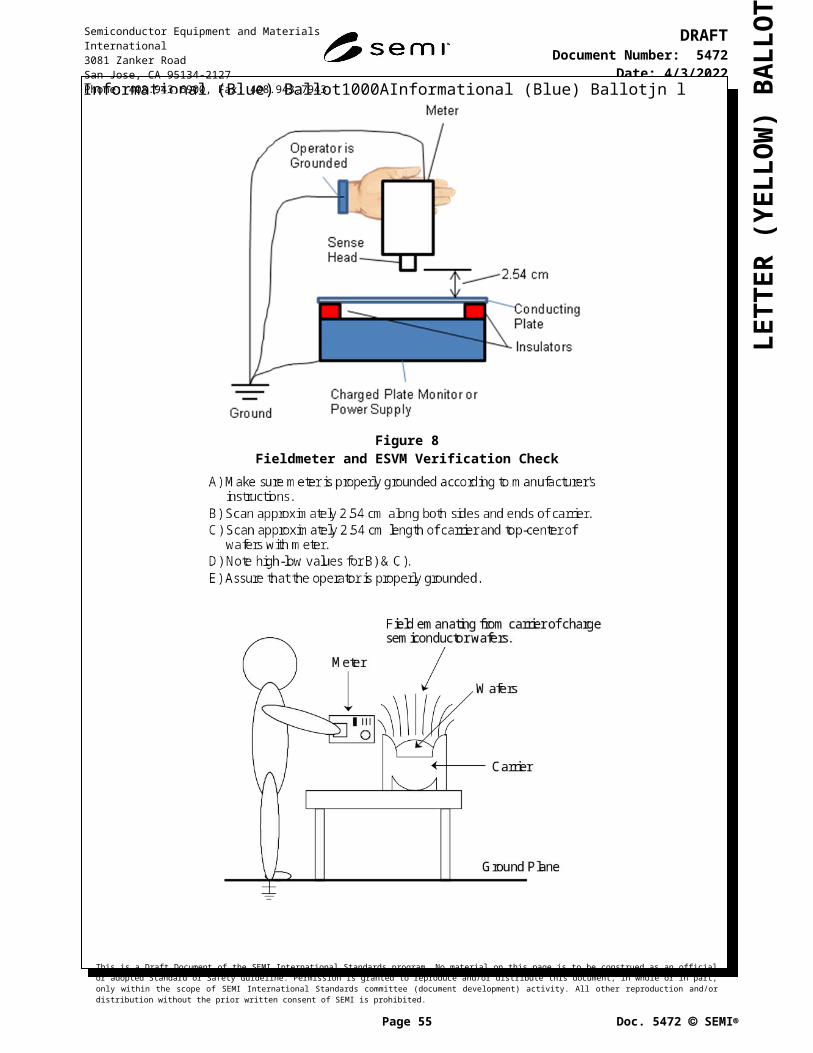
LETT
ER (Y
ELLO
W) B
ALL
OT
Informational (Blue) Ballot1000AInformational (Blue) Ballotjn lmethods to verify the integrity of the ground path to equipment parts, as well as to determine if the product is being charged during its passage through the equipment. The test methods are applicable during the original design of the equipment and during acceptance testing by the end user.
R4-3.2 While the test methods of EOS/ESD SP 10.1-2000 can also be used for periodic verification of the equipment performance, they have one drawback. The automated equipment should be taken off-line to do the testing. This means that there is lost production time, and often the periodic testing is eliminated to maintain product throughput. Other test methods are available that can be performed with the equipment operating online, without altering or disturbing its operation.
R4-4 ESD and EMIR4-4.1 When ESD occurs, the discharge time is usually 10 ns or less. Discharging energy in this short time interval results in the generation of broadband electromagnetic radiation23, as well as the heat that damages semiconductor components. This electromagnetic radiation, especially in the 100 MHz to 2 GHz frequency range, is the electromagnetic interference (EMI) that can affect the operation of production equipment. In addition to ESD damage to semiconductor devices and reticles, ESD-caused EMI results in a variety of equipment operating problems including stoppages, software errors, testing and calibration inaccuracies, and mishandling causing physical component damage.
R4-4.2 EMI Locators — When component damage or equipment problems due to ESD are suspected, it may be useful to detect the EMI generated by the ESD event. This type of testing is both a starting point for determining that electrostatic charge has been generated, and it is a measurement point to ascertain that any electrostatic-charge- control methods have been successful. EMI locators measure dynamic operating conditions, as it is usually not necessary to interrupt equipment operations to make measurements.
R4-4.3 Types of EMI Locators — EMI locators are available in a number of different forms. In its simplest form, it consists of an amplitude modification (AM) radio tuned off station. A popping noise will be heard when an ESD event occurs. At the most complex it consists of a wideband (i.e., greater than 1 GHz) digital storage oscilloscope with a set of appropriate antennas, probes, and software. Measurements of radiated interference can be made using antennas while probes can be connected to equipment parts or electronics and power lines.
R4-4.3.1 An oscilloscope attached to a single antenna can assist in pinpointing the actual location of the ESD event.8, 24, 25, 26 A set of antennas can be used to not only detect the presence of an ESD event, but to determine the location of the pulse in three dimensions.27, 28 Using the same concept as a global positioning system (GPS), the difference in the arrival times of the signal to multiple antennas is directly related to the difference in the distance of each antenna from the ESD source. With the time deltas and the locations of the antennas known, the location of the spark can be uniquely identified employing the appropriate analysis program.
R4-4.3.2 Several other types of EMI-locating equipment are currently in use. Most consist of high-frequency receiving circuitry followed by level detectors to determine the magnitude of the signal. For the purpose of detecting EMI from ESD events, the equipment should have some way of differentiating the short impulse of EMI from the ESD event from the continuous high-frequency radiation of other EMI sources. Some instruments contain a counter to total the number of ESD events above the threshold, or alarms to indicate when the number of ESD events exceeds a preset number. This type of instrument can be placed near the equipment that is suspected of causing ESD events and left in place to monitor.
R4-4.3.3 Several EMI locators are battery-operated, handheld devices that can be easily carried around a facility or placed directly in equipment to check for ESD events. This allows the EMI locator to detect signals that might
23 Tonoya, Watanabe and Honda, “Impulsive EMI Effects from ESD on Raised Floor,” 1994 EOS/ESD Symposium, pp. 164-169, ESD Association.24 Takai, Kaneko and Honda, “One of the Methods of Observing ESD Around Electronic Equipments,” 1996 EOS/ESD Symposium, pp. 186-192, ESD Association.25 Greason, Bulach and Flatley, “Non-Invasive Detection and Characterization of ESD Induced Phenomena in Electronic Systems,” 1996 EOS/ESD Symposium, pp. 193-202, ESD Association.26 Smith, “A New Type of Furniture ESD and Its Implications,” 1993 EOS/ESD Symposium, pp. 3-7, ESD Association.27 Bernier, Croft, and Lowther “ESD Sources Pinpointed by Analysis of Radio Wave Emissions,” Journal of Electrostatics (44) pp. 149-157, Nov. 1998, Elsevier Science B.V., P.O. Box 211, 1000 AE Amsterdam Netherlands.28 Lin, DeChiaro and Jon, “A Robust ESD Event Locator System with Event Characterization,” 1997 EOS/ESD Symposium, pp. 88-98, ESD Association.
This is a Draft Document of the SEMI International Standards program. No material on this page is to be construed as an official or adopted Standard or Safety Guideline. Permission is granted to reproduce and/or distribute this document, in whole or in part, only within the scope of SEMI International Standards committee (document development) activity. All other reproduction and/or distribution without the prior written consent of SEMI is prohibited.
Page 55 Doc. 5472 SEMI
Semiconductor Equipment and Materials International3081 Zanker RoadSan Jose, CA 95134-2127Phone: 408.943.6900, Fax: 408.943.7943
DRAFTDocument Number: 5472
Date: 5/16/2023
LETT
ER (Y
ELLO
W) B
ALL
OT
Informational (Blue) Ballot1000AInformational (Blue) Ballotjn lotherwise be shielded by the equipment’s cover panels. Note that EMI shielding is usually an important part of the design of most production equipment to prevent radiation from the equipment. This makes the detection of ESD events outside the equipment more difficult. It allows pinpointing of the location of an ESD event, which can then be correlated to particular equipment operations.8, 29
R4-4.4 Limitation in Using EMI Locators
R4-4.4.1 One caution needs to be observed when using EMI locators to detect ESD events that cause component damage. The signal received by these devices is generated in areas usually surrounded by grounded metal components. It may have to pass through equipment panels and travel some distance through the air before it reaches the detector. There maybe other radio-frequency (RF) sources and reflecting or absorbing materials in the area. The actual location of the ESD event may be a considerable distance from the EMI locator. It will be difficult to establish any correlation between the amplitude of the signal received by the EMI locator and the energy in the ESD event that produced the signal. The EMI locator primarily indicates the occurrence of an ESD event and can be used to illustrate that a particular electrostatic-charge-control method has eliminated it. It should not be assumed that every ESD event detected results in damage to components or equipment problems. Additional testing will be needed to establish that connection.
R4-5 ESD Event DetectorsR4-5.1 ESD event detectors (EED) are devices that are installed directly on products to detect the presence of an ESD event. They may be attached in proximity to an ESD-sensitive component, connected to the external device leads, or integrated into the device package. Typically they detect the current pulse of an ESD event through an antenna or direct connection to the device circuitry.
R4-5.2 EEDs can be useful in determining the occurrence of ESD events in operating production equipment. The EED has the ability to indicate ESD events of a known level, aiding in the design and performance verification of automated equipment. While costly analysis of failed devices can also provide this information, correlation to equipment operations is usually difficult. An EED that can be monitored optically as it passes through operating equipment provides a convenient method to verify that automated equipment is not generating levels of electrostatic charge that result in ESD damage.
R4-6 Types of EED DevicesR4-6.1 In some EED devices, the signal is amplified and processed to produce a reflectance change in the built-in liquid crystal display (LCD). The EED is designed to trip at a predetermined threshold voltage, detecting ESD transients above the selected amplitude. Some devices can be reset magnetically or optically making them reusable.
R4-6.2 Other devices use the controllable ESD-damage threshold of metal-oxide-semiconductor field-effect transistors (MOSFETs). The test methodology is to amplify an ESD transient to create sufficient energy to destroy the gate oxide. The device may be used until the specified ESD level is achieved, and then the EED fails. A similar device is based on the metal-oxide-semiconductor capacitor (MOSCAP). The current leakage through the device significantly increases if the ESD amplitude is sufficient to damage the MOS structure. Both of these types of EED are removed from where they are installed and require additional instrumentation to determine their status.
R4-6.3 Another type of EED employs the magnetic fields from a current flow to affect a series of magneto-optic thin films. The magnetic field from the ESD current alters the film’s magnetic state and affects the degree of polarization of visible light reflected from the film. Varying the distance between the film and the ESD current-carrying conductor indicates different thresholds. This EED can be read using a microscope equipped with a polarizing element and does not need to be removed from the circuitry to be read. It can be reset with a magnet.30
R4-7 ConclusionR4-7.1 There is little question that electrostatic-charge problems continue to result in significant losses in high-technology manufacturing. Increasingly, electrostatic-charge-control methods are applied in the equipment that produces the product. It will be important to develop and utilize a range of diagnostic methods and measurement equipment for ESD in equipment.
29 Fujie, A., “Pinpointing Sources of Static Electricity with EMI Locator,” Parts 1 and 2, Nikkei Electronics Asia, December 1992 and January 1993, Nikkei Business Publications Asia Ltd., 533 Hennessy Road, Causeway Bay, Hong Kong.30 Jackson, Tan, and Boehm, “Magneto Optical Static Event Detector,” 1998 EOS/ESD Symposium, pp.233-244, ESD Association.
This is a Draft Document of the SEMI International Standards program. No material on this page is to be construed as an official or adopted Standard or Safety Guideline. Permission is granted to reproduce and/or distribute this document, in whole or in part, only within the scope of SEMI International Standards committee (document development) activity. All other reproduction and/or distribution without the prior written consent of SEMI is prohibited.
Page 56 Doc. 5472 SEMI
Semiconductor Equipment and Materials International3081 Zanker RoadSan Jose, CA 95134-2127Phone: 408.943.6900, Fax: 408.943.7943
DRAFTDocument Number: 5472
Date: 5/16/2023

LETT
ER (Y
ELLO
W) B
ALL
OT
Informational (Blue) Ballot1000AInformational (Blue) Ballotjn l
REVISION RECORDCHANGES IN THIS DOCUMENT FROM E43-0301NOTICE: The following information is provided to track revisions to this Document. Negative votes may not be cast against this information. Changes may be submitted to Standards Staff via a Publication Improvement Proposal (PIP) form available from the SEMI Standards Web site.
Cycle Authorization Section Description
1108 Ballot 4241 Entire Document
Complete rewrite:Title — Change of the document title from: “Guide For Measuring Static Charge On Objects And Surfaces” to “Recommended Practice for Electrostatic Measurements on Objects and Surfaces.”Purpose — Change of the purpose of the document from: “to establish a guide for reproducible measurement of electrostatic charge(s)” to “to establish a guide for reproducible electrostatic measurements.”Scope — The scope of the document was broadened by including voltage, field level(s) and electrostatic discharge measurements (¶2.1). The applicability of the standard was identified as ‘semiconductor manufacturing environments.”Limitations — Minor revisions to ¶ 3.1, 3.2 and ¶ 3.3.Terminology — Definition of “Ground” moved from ¶5.3 to ¶5.2.Safety Precautions — The title of the paragraph changed, updates to ¶¶ 6.1–6.3.Equipment — Major changes: definitions of the equipment, removed performance verification and zeroing procedures descriptions - those were moved to § 9 Test and Measurement. Table 1, Test Voltages, was also moved to § 9.Sufficient Number of Measurements — Title of the section changed from “Sampling.” The section was updated with more precise recommendations.Test Methods and Measurements — Significant updates to all paragraphs. Table 2, Measurement Units, was removed as it is no longer relevant. A new paragraph, ¶ 9.4 Electrostatic Discharge Measurements, was added.Certification — Updates to all paragraphs in this section.Documentation — Updates to ¶ 11.1. New Figure 2.Related Documents — Updates to reflect recent changes and revisions to the referenced documents.Appendix 1, Measurement Selection Matrix — Numerous changes to ¶ A1.1. Table A1-1 Measurement Method Recommendations replaced by two separate tables: Table A1-1 Recommended Instruments for Electric Charge Measurements, and Table A1-2 Recommended Instruments for ESD Event Measurements.Related Information 1, Notes on Equipment — Minor updates to all paragraphs.
0213 Ballot 5472 1.0 Title — Change of the Document title from: “Recommended Practice for Electrostatic Measurements on Objects and Surfaces.” to “Guide for Electrostatic Measurements on Objects and Surfaces”.
0213 Ballot 5472 5.1 Added new acronyms and used them throughout the Document0213 Ballot 5472 7.4, 9.4 Added information on the high-impedance contacting digital voltmeter (HIDVM)0213 Ballot 5472 12.3 Added ESD Association Symposium proceedings0213 Ballot 5472 Appendix
A1Added HIDVM to Table A1-1
0213 Ballot 5472 Related Information R1-3
Added procedure to determine the effect of the HIDVM on the accuracy of measurements.
This is a Draft Document of the SEMI International Standards program. No material on this page is to be construed as an official or adopted Standard or Safety Guideline. Permission is granted to reproduce and/or distribute this document, in whole or in part, only within the scope of SEMI International Standards committee (document development) activity. All other reproduction and/or distribution without the prior written consent of SEMI is prohibited.
Page 57 Doc. 5472 SEMI
Semiconductor Equipment and Materials International3081 Zanker RoadSan Jose, CA 95134-2127Phone: 408.943.6900, Fax: 408.943.7943
DRAFTDocument Number: 5472
Date: 5/16/2023
LETT
ER (Y
ELLO
W) B
ALL
OT
Informational (Blue) Ballot1000AInformational (Blue) Ballotjn lNOTICE: Semiconductor Equipment and Materials International (SEMI) makes no warranties or representations as to the suitability of the Standards and Safety Guidelines set forth herein for any particular application. The determination of the suitability of the Standard or Safety Guideline is solely the responsibility of the user. Users are cautioned to refer to manufacturer’s instructions, product labels, product data sheets, and other relevant literature, respecting any materials or equipment mentioned herein. Standards and Safety Guidelines are subject to change without notice.
By publication of this Standard or Safety Guideline, SEMI takes no position respecting the validity of any patent rights or copyrights asserted in connection with any items mentioned in this Standard or Safety Guideline. Users of this Standard or Safety Guideline are expressly advised that determination of any such patent rights or copyrights, and the risk of infringement of such rights are entirely their own responsibility.
This is a Draft Document of the SEMI International Standards program. No material on this page is to be construed as an official or adopted Standard or Safety Guideline. Permission is granted to reproduce and/or distribute this document, in whole or in part, only within the scope of SEMI International Standards committee (document development) activity. All other reproduction and/or distribution without the prior written consent of SEMI is prohibited.
Page 58 Doc. 5472 SEMI
Semiconductor Equipment and Materials International3081 Zanker RoadSan Jose, CA 95134-2127Phone: 408.943.6900, Fax: 408.943.7943
DRAFTDocument Number: 5472
Date: 5/16/2023