jupiter.math.nctu.edu.twweng/courses/ic... · abstract technology migration for hard ips fang fang...
TRANSCRIPT

TECHNOLOGY MIGRATION FOR HARD IPS
by
Fang Fang
A thesis submitted in conformity with the requirementsfor the degree of Master of Applied Science
Graduate Department of Electrical and Computer EngineeringUniversity of Toronto
Copyright c© 2003 by Fang Fang
Abstract
Technology Migration for Hard IPs
Fang Fang
Master of Applied Science
Graduate Department of Electrical and Computer Engineering
University of Toronto
2003
As the foundries accelerate their update of advanced processes with increasingly complex de-
sign rules, the cost of hard intellectual property (IP) development becomes prohibitively high.
A technology migration tool that can port hard IPs from old technology to new technology is
presented in the thesis. The thesis makes four primary contributions: First, it proposes a new
fast design rule constraint generation algorithm that further limits the searcing spaces. Second,
it introduces a dual-pass strategy to solve the high level layout architecture constraints for mi-
grating all the library leaf cells. Third, it proposes a new optimization metric, called geometric
closessness, that can help retain advanced design intention. Finally, soft constraints method
is proposed to trace the conflicting constraints specified by the users. We test our migration
tool by successfully migrating Berkeley low power libraries, originally developed for 1.2um
MOSIS process to TSMC 0.25um and 0.18um technologies.
ii

Acknowledgements
iii

Contents
1 Introduction 1
1.1 Motivation . . . . . . . . . . . . . . . . . . . . . . . . . . . . . . . . . . . . . 3
1.2 Contribution . . . . . . . . . . . . . . . . . . . . . . . . . . . . . . . . . . . . 3
1.3 Organization of thesis . . . . . . . . . . . . . . . . . . . . . . . . . . . . . . . 4
2 Background 5
2.1 Virtual Grid Compaction and Shear-line Compaction . . . . . . . . . . . . . . 5
2.2 Constraint Graph Compaction .. . . . . . . . . . . . . . . . . . . . . . . . . 7
2.3 Hierarchical Layout Compaction. . . . . . . . . . . . . . . . . . . . . . . . . 11
2.4 Other Developments . . . . . . . . . . . . . . . . . . . . . . . . . . . . . . . 12
3 Migration Engine 15
3.1 Background . . . .. . . . . . . . . . . . . . . . . . . . . . . . . . . . . . . . 15
3.2 Migration Engine . . . . . . . . . . . . . . . . . . . . . . . . . . . . . . . . . 28
3.3 Design Rule Constraint Generation . . . . . .. . . . . . . . . . . . . . . . . . 30
3.4 Objective function . . . . . . . . . . . . . . . . . . . . . . . . . . . . . . . . . 46
3.5 Integer Linear Programming Solver . . . . . . . . . . . . . . . . . . . . . . . 51
4 Migration for datapath and standard cell libraries 52
4.1 Datapath library migration . . .. . . . . . . . . . . . . . . . . . . . . . . . . 52
4.2 Standard Cell Library Migration. . . . . . . . . . . . . . . . . . . . . . . . . 61
iv
5 Experiments and Conclusion 67
5.1 Experimental Setup . . . . . . . . . . . . . . . . . . . . . . . . . . . . . . . . 67
5.2 Experimental Result . . . . . . . . . . . . . . . . . . . . . . . . . . . . . . . . 68
5.3 Limiation . . . . . . . . . . . . . . . . . . . . . . . . . . . . . . . . . . . . . 76
5.4 Conclusion . . . . . . . . . . . . . . . . . . . . . . . . . . . . . . . . . . . . 78
5.5 Future work . . . . . . . . . . . . . . . . . . . . . . . . . . . . . . . . . . . . 79
6 Appendix 80
Bibliography 96
v

List of Tables
5.1 Layout architecture characteristics . . . . . .. . . . . . . . . . . . . . . . . . 71
5.2 Layout structure characteristics .. . . . . . . . . . . . . . . . . . . . . . . . . 75
5.3 User specified layout architecture requirements for cell haf001 . .. . . . . . . 78
6.1 Experiment results of datpath library migration. . . .. . . . . . . . . . . . . . 82
6.2 Experiment results for standard cell library migration.. . . . . . . . . . . . . . 84
vi

List of Figures
1.1 A general architecture of SoC. .. . . . . . . . . . . . . . . . . . . . . . . . . 2
2.1 Before virtual grid compaction. . . . . . . . . . . . . . . . . . . . . . . . . . 6
2.2 After virtual grid compaction. . . . . . . . . . . . . . . . . . . . . . . . . . . 6
2.3 A spacing constraint is presented by an edge in the directed graph.. . . . . . . 7
2.4 A’s shadow is blocked by B. So there is no edge between A ad C in the con-
straint graph. . . . . . . . . . . . . . . . . . . . . . . . . . . . . . . . . . . . 8
2.5 Each circuit element is expanded by D/2 in both positive and negative X direc-
tions. The elements that stay within the same slot in scanning bar are recorded
in the same X coordinate bin. . . . . . . . . . . . . . . . . . . . . . . . . . . . 9
2.6 The constraint graph for a cell to be pitch matched. .. . . . . . . . . . . . . . 11
2.7 Port abstraction method. . . . .. . . . . . . . . . . . . . . . . . . . . . . . . 12
2.8 Wire jogging. . . .. . . . . . . . . . . . . . . . . . . . . . . . . . . . . . . . 13
3.1 A layout is composed of several planes. . . .. . . . . . . . . . . . . . . . . . 16
3.2 The tile structure in metal1 plane . . . . . .. . . . . . . . . . . . . . . . . . 18
3.3 The process to find right neighor tiles. . . . .. . . . . . . . . . . . . . . . . . 21
3.4 The process to locate the tile that contains a given point . . . . . .. . . . . . . 23
3.5 Tile enumeration. . . . . . . . . . . . . . . . . . . . . . . . . . . . . . . . . . 26
3.6 Each edge rule can be applied in any of the four directions. . . . .. . . . . . . 26
3.7 An example of edge rule. . . . . . . . . . . . . . . . . . . . . . . . . . . . . . 27
vii

3.8 Tiles are aligned in grids . . . . . . . . . . . . . . . . . . . . . . . . . . . . . 29
3.9 Each tile has new position and shape after migration with no design rule viola-
tions. . . . . . . . . . . . . . . . . . . . . . . . . . . . . . . . . . . . . . . . 30
3.10 Design rule checker looks for non-OKType tiles within constraint region. . . . 31
3.11 (a) An example layout in active plane. The shaded rectangles 1, 3, 5, 6 and 10
represent poly tiles. Rectangle 8 is diffusion tile. Other rectangles are all space
tiles. (b) The constraint graph generated from poly spacing rule. .. . . . . . . 32
3.12 (a) A fraction of a layout plane. Tile 1 is the source tile that is being pro-
cessed for edge rule constraint generation. (b) Depth-K shadowing neighbor-
hood graph for tile 1. . . . . . .. . . . . . . . . . . . . . . . . . . . . . . . . 34
3.13 The best case for Depth-K searching algorithm . . .. . . . . . . . . . . . . . 37
3.14 The maximum number of tiles to be visited for tile s .. . . . . . . . . . . . . . 38
3.15 A leaf cell muxf201. . . . . . .. . . . . . . . . . . . . . . . . . . . . . . . . 38
3.16 The constraint graph for IntraPlane constraints. . . .. . . . . . . . . . . . . . 39
3.17 Corner constraint region checking . . . . . .. . . . . . . . . . . . . . . . . . 39
3.18 (a) In the old layout, tile 3 doesn’t overlap with tile s in X direction. (b) After
X direction migration and Y direction migration, tile 3 moves into shadow area
of tile 1. (c) Interpass Constraint graph for tile s (d) Interpass constraints for
tile s. . . . . . . . . . . . . . . . . . . . . . . . . . . . . . . . . . . . . . . . 40
3.19 N-well tile stays on well plane while diffusion tile stays on active plane. . . . . 42
3.20 (a)The Depth-K shadowing neighborhood graph for interplane edge rule (b)
InterPlane edge rule constraint between source tiles and tile3. . . . . . . . . . 43
3.21 InterPlane constraints generated for cell muxf201. . .. . . . . . . . . . . . . . 44
3.22 A contact has different tile types on the planes it connects. The poly contact in
this figure haspcontact tile (tile 1) on active plane andpcontact/metal1 tile
(tile 2) on metal1 plane. . . . . . . . . . . . . . . . . . . . . . . . . . . . . . . 45
3.23 Connect constraints generated for cell muxf201. . . .. . . . . . . . . . . . . . 46
viii
3.24 Tile1 is the leftmost tile in a layout andxl is the X coordinate of its left edge.
Tile 2 is the rightmost tile in the layout andxr is the X coordinate of its right
edge. . . . . . . . . . . . . . . . . . . . . . . . . . . . . . . . . . . . . . . . . 47
3.25 The old layout and migrated layout with minimum perturbation objective func-
tion. . . . . . . . . . . . . . . . . . . . . . . . . . . . . . . . . . . . . . . . . 49
3.26 The old layout and migrated layout with geometric closeness objective function. 50
4.1 An 8-bit adder block diagram. . . . . . . . . . . . . . . . . . . . . . . . . . . 53
4.2 An 8-bit adder constructed by abutting 8 adder bitslices and 1 control slice. . . 54
4.3 An example of datapath library cell. . . . . .. . . . . . . . . . . . . . . . . . 54
4.4 Port matching of leaf cells. . . . . . . . . . . . . . . . . . . . . . . . . . . . . 55
4.5 Dual-pass migration strategy. . . . . . . . . . . . . . . . . . . . . . . . . . . . 57
4.6 Cell with routing track for data signals. . . . .. . . . . . . . . . . . . . . . . . 58
4.7 The width of each power net has to be equal topw given by the designer in the
specification file. . . . . . . . . . . . . . . . . . . . . . . . . . . . . . . . . . 59
4.8 Standard cells design . . . . . . . . . . . . . . . . . . . . . . . . . . . . . . . 62
4.9 Layout architecture for a standard cell library.. . . . . . . . . . . . . . . . . . 63
4.10 All I/O ports stay in fixed grids . . . . . . . . . . . . . . . . . . . . . . . . . . 64
4.11 The requirements on power rails . . . . . . . . . . . . . . . . . . . . . . . . . 65
5.1 The run time of design rule constraint generation . .. . . . . . . . . . . . . . 69
5.2 The run time of ILP solver. . . . . . . . . . . . . . . . . . . . . . . . . . . . . 70
5.3 The leafcells for ripple carry adder . . . . . .. . . . . . . . . . . . . . . . . . 71
5.4 The floorplane of an N bit adder. . . . . . . . . . . . . . . . . . . . . . . . . . 72
5.5 Migration of a four-bit adder . . . . . . . . . . . . . . . . . . . . . . . . . . . 73
5.6 Two old standard cells based on standard MOSIS1.2µm technology. . . . . . . 74
5.7 Migrated cells based on TSMC 0.18µm technology. .. . . . . . . . . . . . . . 74
ix

5.8 The migration results under geometric closeness objective function and mini-
mum perturbation objective function. . . . . . . . . . . . . . . . . . . . . . . . 76
5.9 Cell haf001 before migration . . . . . . . . . . . . . . . . . . . . . . . . . . . 76
5.10 Cell haf001 after migrated towards TSMC 0.18µm technology. . .. . . . . . . 77
5.11 The design rule requirements on power rail. . . . . . . . . . . . . . . . . . . . 77
x
Chapter 1
Introduction
The ASIC technology has evolved from a chip-set philosophy to system-on-chip (SoC) con-
cept. SoC is generally defined asan IC designed by stitching multiple stand-alone VLSI de-
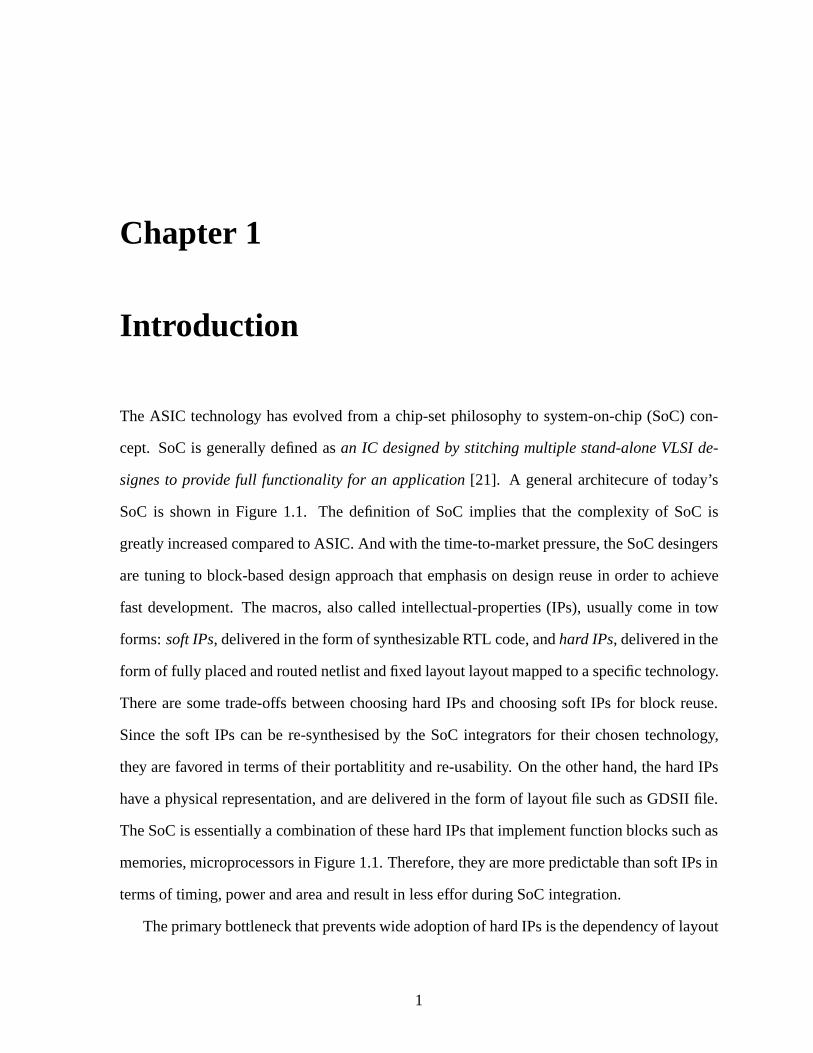
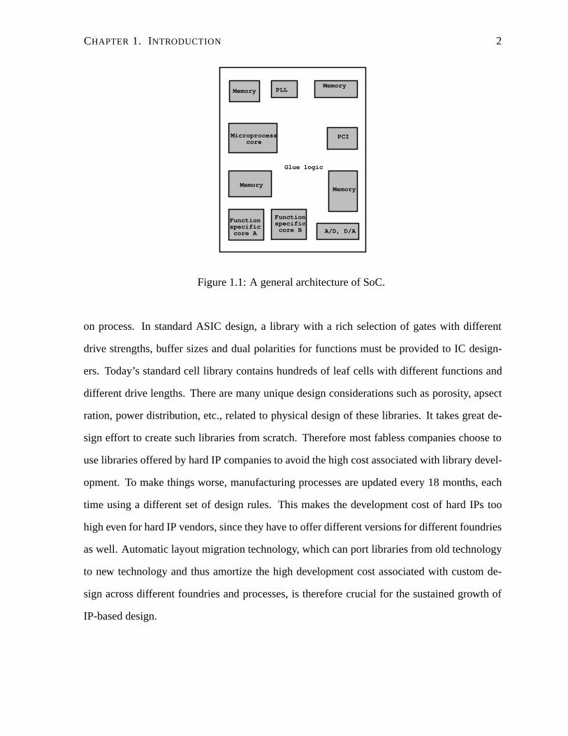
signes to provide full functionality for an application[21]. A general architecure of today’s
SoC is shown in Figure 1.1. The definition of SoC implies that the complexity of SoC is
greatly increased compared to ASIC. And with the time-to-market pressure, the SoC desingers
are tuning to block-based design approach that emphasis on design reuse in order to achieve
fast development. The macros, also called intellectual-properties (IPs), usually come in tow
forms:soft IPs, delivered in the form of synthesizable RTL code, andhard IPs, delivered in the
form of fully placed and routed netlist and fixed layout layout mapped to a specific technology.
There are some trade-offs between choosing hard IPs and choosing soft IPs for block reuse.
Since the soft IPs can be re-synthesised by the SoC integrators for their chosen technology,
they are favored in terms of their portablitity and re-usability. On the other hand, the hard IPs
have a physical representation, and are delivered in the form of layout file such as GDSII file.
The SoC is essentially a combination of these hard IPs that implement function blocks such as
memories, microprocessors in Figure 1.1. Therefore, they are more predictable than soft IPs in
terms of timing, power and area and result in less effor during SoC integration.
The primary bottleneck that prevents wide adoption of hard IPs is the dependency of layout
1
CHAPTER 1. INTRODUCTION 2
Memory PLLMemory
Microprocess core
MemoryMemory
Functionspecific core A
Functionspecific core B A/D, D/A
Glue logic
PCI
Figure 1.1: A general architecture of SoC.
on process. In standard ASIC design, a library with a rich selection of gates with different
drive strengths, buffer sizes and dual polarities for functions must be provided to IC design-
ers. Today’s standard cell library contains hundreds of leaf cells with different functions and
different drive lengths. There are many unique design considerations such as porosity, apsect
ration, power distribution, etc., related to physical design of these libraries. It takes great de-
sign effort to create such libraries from scratch. Therefore most fabless companies choose to
use libraries offered by hard IP companies to avoid the high cost associated with library devel-
opment. To make things worse, manufacturing processes are updated every 18 months, each
time using a different set of design rules. This makes the development cost of hard IPs too
high even for hard IP vendors, since they have to offer different versions for different foundries
as well. Automatic layout migration technology, which can port libraries from old technology
to new technology and thus amortize the high development cost associated with custom de-
sign across different foundries and processes, is therefore crucial for the sustained growth of
IP-based design.
CHAPTER 1. INTRODUCTION 3
1.1 Motivation
Layout migration tools available today cannot cope with all the challenges involved. First,
most migration tools are based on layout compaction, a technology developed a decade ago,
when the layout area is the primary concern. Layout compaction tends to compress space
between polygons recklessly as long as design rules are not violated. In modern design us-
ing aggressive circuit styles in deep submicron processes, space is often among the first class
citizens ofadvanced layout considerations, for example, to combat signal integrity. Other spe-
cializedadvanced circuit considerations, such as new transistor sizes, device matching, are
rarely considered in an integrated fashion. Second, most techniques reported in the literature
are designed to migrate a specific circuit that uses a library of cells, rather than the library
itself. Without considering theoverall library architecturesuch as power/ground net width,
routing track number and port matching, the cell layouts migrated under this circuit-driven
strategy work only for the specific circuits, so there is no guarantee that they work under all
occasions, and each time a new circuit is migrated, all the leaf cells in the whole library need
to be migrated again.
1.2 Contribution
An integer linear programming (ILP) based migration framework which is customized for dat-
apath IP and standard cell IP migration is presented in this thesis. New libraries based on new
technologies can be generated when given the libraries of the old process and new library ar-
chitecture specifications. Several innovations that help solve the difficult problems discussed
earlier are listed below:
• A new design rule generation algorithm,Depth-K searching algorithm, which takes less
searching effort than the shadow propagation method currently employed for constraint
generation [18], is used in this project.
CHAPTER 1. INTRODUCTION 4
• A new optimization objective, calledgeometric closeness, to reward geometric resem-
blance of migrated layout to the original layout is introduced in this project. Under this
metric, space is explicitly represented. Preservation of space and non-space polygons is
given equal priority. This ensures that the original layout design considerations are not
corrupted
• In order to address the overall library architecture requirements, adual-pass strategyis
employed in the migration tool that helps meet high level layout architecture constraints.
This is in contrast to the top-down constraint propagation strategy employed by tradi-
tional hierarchical compactors, which are limited only to area minimization.
• Since the library architecture is specified by users, they may conflict with design rules,
which will lead to an infeasible solution. A new concept, calledsoft constraints, is pro-
posed in order to obtain a best-effort solution. A concrete feedback is provided where ar-
chitecture requirements fail, which thereby helps the user interactively define the proper
library architecture.
1.3 Organization of thesis
The rest of the thesis is organized as follows: First a review of previous work is given in chapter
2. Then a detailed discussion of the basic migration engine implementation is presented in
chapter 3. Chapter 4 talks about what are the specific layout architecture requirements for
datapath library and standard cell library and how the requirements are solved with the dual-
path approach. The experimental results are given in Chapter 5. Finally, Chapter 6 gives the
conclusion and summarizes the future work.
Chapter 2
Background
Automatic layout migration was among the oldest CAD problems investigated and a large
body of research was carried out under the layout compaction problem. Surveys of layout
compaction can be found in [6] and [9]. Early compactors are performed on symbolic layout
in which circuit elements are presented by simple lines or rectangles, known assticks. The
symbolic layout compaction methodologies include shear-line approach, virtual grid approach
and constraint graph approach, which will be discussed in the following sections.
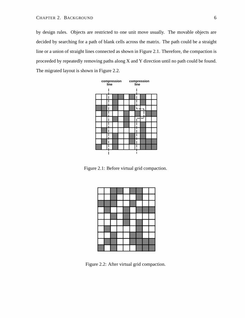
2.1 Virtual Grid Compaction and Shear-line Compaction
Commercial layout systems such asMULGA [25] use the virtual grid compaction approach
to compress the layout. Once the symbolic layout is generated, the virtual grid compaction
method compresses space by moving objects. The procedure includes two main steps:
• search for movable objects by consultation with layout topology and design rules;
• perform the compaction by moving these objects.
In order to identify the movable objects and the moving distance, the layout is represented
by am× n matrix as shown in Figure 2.1. Each entry of the matrix represents a mask element
marked as a shaded cell or space marked as a blank cell. The size of the grid unit is determined
5
CHAPTER 2. BACKGROUND 6
by design rules. Objects are restricted to one unit move usually. The movable objects are
decided by searching for a path of blank cells across the matrix. The path could be a straight
line or a union of straight lines connected as shown in Figure 2.1. Therefore, the compaction is
proceeded by repeatedly removing paths along X and Y direction until no path could be found.
The migrated layout is shown in Figure 2.2.
compression line
compression line
Figure 2.1: Before virtual grid compaction.
Figure 2.2: After virtual grid compaction.

CHAPTER 2. BACKGROUND 7
The shear-line approach is very similar to virtual grid compaction except that the grid spac-
ing is fixed to the worst case design rule [8] [1].
The compaction is made easy with the matrix representation of the layout. However, the
grid size must be carefully decided because coarse grid results in smaller matrix and thus less
run time, but the compaction may not be efficient. On the other hand, high grid resolution will
lead to large matrix and thus slow down the run time. Another disadvantage of this compaction
method is that the optimization goal can only be the minimization of the layout area. With this
approach, no other optimization goals can be achieved.
2.2 Constraint Graph Compaction
The constraint graph compaction was first discussed by Hsueh and Pederson [18]. Many other
compaction tools such asFLOSS [5], CABBAGE [18] andSLIM [1], use this strategy to
compact layouts. In this approach, the topology constraints and design rule requirements are
presented with a weighted directed graph, calledconstraint graph. Each vertex represents a
circuit element. For each spacing constraint between two elements, there is an arc(i, j) with
weightdij.
1 2
1 2
(a) (b)
x x
x x >= d
d
1 2
12 12
12
−
Figure 2.3: A spacing constraint is presented by an edge in the directed graph.
The new position of each element can be obtained either by running longest path algorithm
or by using linear programming solver depending on the optimization goal the user chooses.
Because of its flexibility, we adopt this approach in our migration tool.
CHAPTER 2. BACKGROUND 8
2.2.1 Constraint Generation
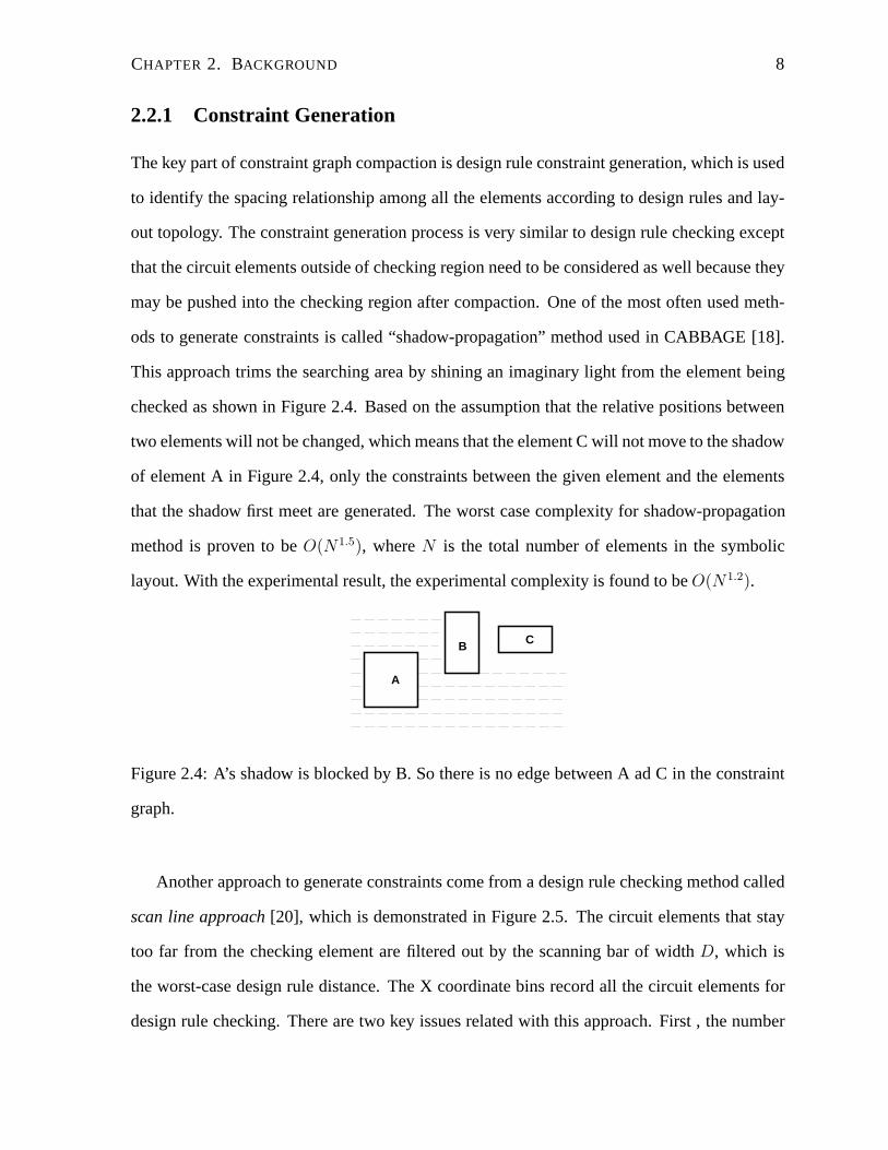
The key part of constraint graph compaction is design rule constraint generation, which is used
to identify the spacing relationship among all the elements according to design rules and lay-
out topology. The constraint generation process is very similar to design rule checking except
that the circuit elements outside of checking region need to be considered as well because they
may be pushed into the checking region after compaction. One of the most often used meth-
ods to generate constraints is called “shadow-propagation” method used in CABBAGE [18].
This approach trims the searching area by shining an imaginary light from the element being
checked as shown in Figure 2.4. Based on the assumption that the relative positions between
two elements will not be changed, which means that the element C will not move to the shadow
of element A in Figure 2.4, only the constraints between the given element and the elements
that the shadow first meet are generated. The worst case complexity for shadow-propagation
method is proven to beO(N1.5), whereN is the total number of elements in the symbolic
layout. With the experimental result, the experimental complexity is found to beO(N1.2).
A
B C
Figure 2.4: A’s shadow is blocked by B. So there is no edge between A ad C in the constraint
graph.
Another approach to generate constraints come from a design rule checking method called
scan line approach[20], which is demonstrated in Figure 2.5. The circuit elements that stay
too far from the checking element are filtered out by the scanning bar of widthD, which is
the worst-case design rule distance. The X coordinate bins record all the circuit elements for
design rule checking. There are two key issues related with this approach. First , the number
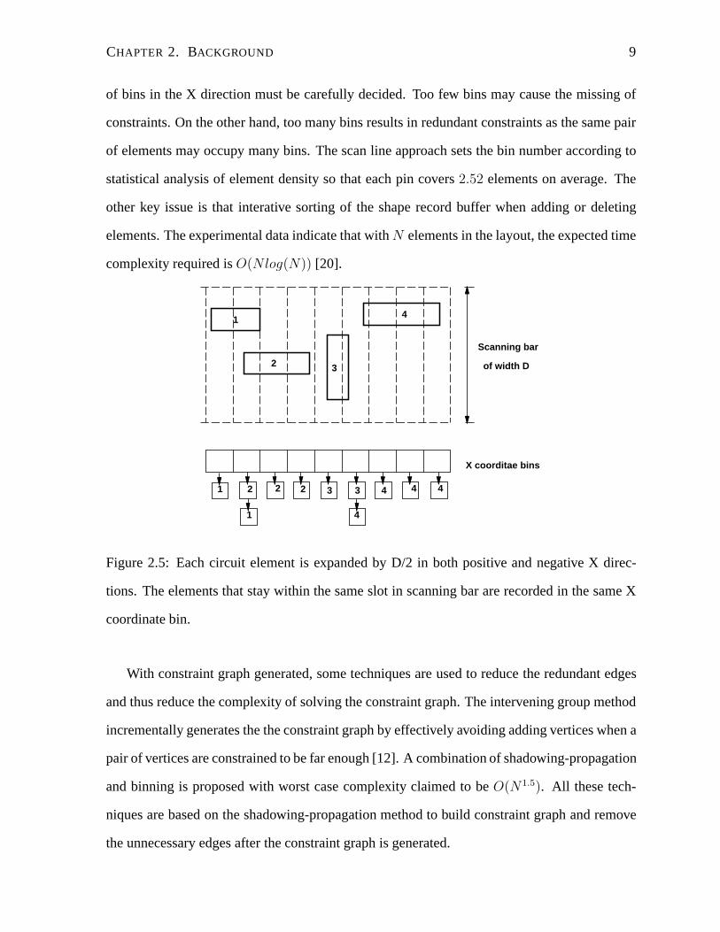
CHAPTER 2. BACKGROUND 9
of bins in the X direction must be carefully decided. Too few bins may cause the missing of
constraints. On the other hand, too many bins results in redundant constraints as the same pair
of elements may occupy many bins. The scan line approach sets the bin number according to
statistical analysis of element density so that each pin covers2.52 elements on average. The
other key issue is that interative sorting of the shape record buffer when adding or deleting
elements. The experimental data indicate that withN elements in the layout, the expected time
complexity required isO(Nlog(N)) [20].
1
2 3
4
1 2
1
2 2 3
4
4 43 4
Scanning bar
of width D
X coorditae bins
Figure 2.5: Each circuit element is expanded by D/2 in both positive and negative X direc-
tions. The elements that stay within the same slot in scanning bar are recorded in the same X
coordinate bin.
With constraint graph generated, some techniques are used to reduce the redundant edges
and thus reduce the complexity of solving the constraint graph. The intervening group method
incrementally generates the the constraint graph by effectively avoiding adding vertices when a
pair of vertices are constrained to be far enough [12]. A combination of shadowing-propagation
and binning is proposed with worst case complexity claimed to beO(N1.5). All these tech-
niques are based on the shadowing-propagation method to build constraint graph and remove
the unnecessary edges after the constraint graph is generated.
CHAPTER 2. BACKGROUND 10
The constraint generation methods discussed above are all performed on sybmolic layout.
In symbolic layout, the circuit elements such as transistor, contact and wire are modelled as
sticks snapped to virtual grids. At symbolic layout level, circuit elements do not have detailed
mask information. The positions of circuit elements are decided by respecting the high level
design rules such as minimum spacing rules and minimum width rule, etc. In order to generate
real mask layout, another process to transform symbolic layout to mask layout is needed after
symbolic layout compaction. In this thesis, we directly migrate the mask layout without taking
the symbolic layout transfromation step. A new constraint generation method applied directly
on mask layout represented in corner stitching data structure, calledDepth-K searching algo-
rithm, is proposed in this thesis that can further reduce the searching area by limiting the depth
it traverses than the shadowing-propagation algorithm. And with corner stitching layout repre-
sentation, it avoids the iterative sorting of shape buffers in scan line approach. The data in the
Appendix show that the experimental run time is proportional toO(N1.4).
2.2.2 Objective Function
After the constraint graph is built, there are two ways to solve the graph. One is to decide each
vertex’s longest path length from the boundary vertex, which amounts to finding the shortest
path algorithm in a directed graph with arc weight negated. Most of early compaction tools
are based on this approach. However, the implied compaction goal of this approach is to min-
imize the layout area. In order to accommodate more compaction goals such as minimization
of power or perturbation, the constraint graph is solved by dumping constraints to linear pro-
gramming solver and obtaining the result under the user specified compaction goal.
Theminimum perturbation objective functionproposed in [10] was the first work that de-
parted from the traditional area minimization optimization goal and argued the importance of
rewarding geometric similarity between the migrated layout and the original layout. However,
the quantitative measure that they develop for geometric similarity is asymmetrical and penal-
izes both right edges in the X direction and upper edges in the Y direction. In our migration
CHAPTER 2. BACKGROUND 11
tool, we slightly modify the minimum perturbation objective function by minimizing the size
change of each rectangle in the layout.
2.3 Hierarchical Layout Compaction
The majority of the hierarchical layout compactors reported in literature focus on solving the
pitch matching problem, which means that certain elements among different cells must match
in size and position when cells are abutted. The method described in [11] first compacts leaf-
cells and then locates the abutting ports to fixed grids. After that, the compacted cells are
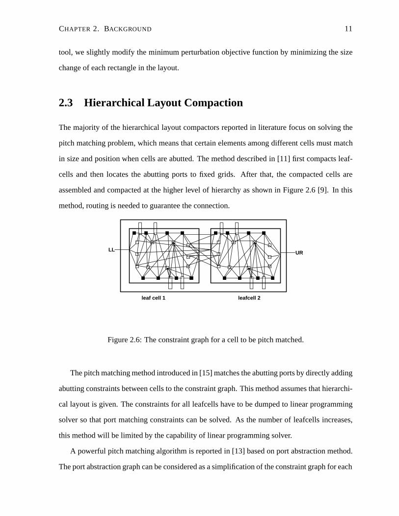
assembled and compacted at the higher level of hierarchy as shown in Figure 2.6 [9]. In this
method, routing is needed to guarantee the connection.
LL UR
leaf cell 1 leafcell 2
Figure 2.6: The constraint graph for a cell to be pitch matched.
The pitch matching method introduced in [15] matches the abutting ports by directly adding
abutting constraints between cells to the constraint graph. This method assumes that hierarchi-
cal layout is given. The constraints for all leafcells have to be dumped to linear programming
solver so that port matching constraints can be solved. As the number of leafcells increases,
this method will be limited by the capability of linear programming solver.
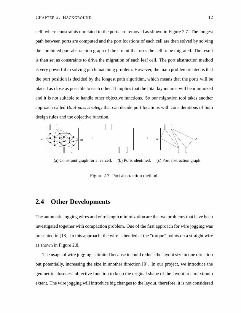
A powerful pitch matching algorithm is reported in [13] based on port abstraction method.
The port abstraction graph can be considered as a simplification of the constraint graph for each
CHAPTER 2. BACKGROUND 12
cell, where constraints unrelated to the ports are removed as shown in Figure 2.7. The longest
path between ports are computed and the port locations of each cell are then solved by solving
the combined port abstraction graph of the circuit that uses the cell to be migrated. The result
is then set as constraints to drive the migration of each leaf cell. The port abstraction method
is very powerful in solving pitch matching problem. However, the main problem related is that
the port position is decided by the longest path algorithm, which means that the ports will be
placed as close as possible to each other. It implies that the total layout area will be minimized
and it is not suitable to handle other objective functions. So our migration tool takes another
approach calledDual-pass strategythat can decide port locations with considerations of both
design rules and the objective function.
LL UR LL LR
(a) Constraint graph for a leafcell. (b) Ports identified. (c) Port abstraction graph
Figure 2.7: Port abstraction method.
2.4 Other Developments
The automatic jogging wires and wire length minimization are the two problems that have been
investigated together with compaction problem. One of the first approach for wire jogging was
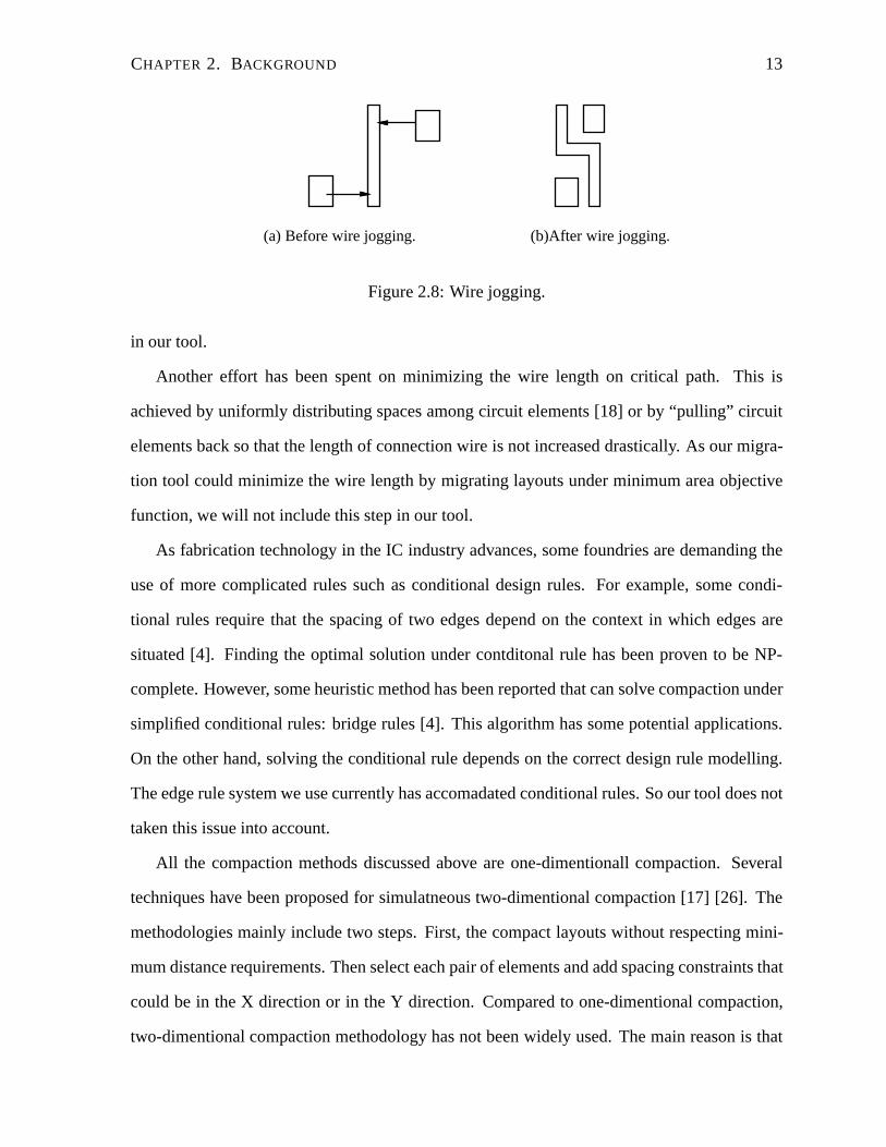
presented in [18]. In this approach, the wire is bended at the “torque” points on a straight wire
as shown in Figure 2.8.
The usage of wire jogging is limited because it could reduce the layout size in one direction
but potentially, increasing the size in another direction [9]. In our project, we introduce the
geometric closeness objective function to keep the original shape of the layout to a maximum
extent. The wire jogging will introduce big changes to the layout, therefore, it is not considered
CHAPTER 2. BACKGROUND 13
(a) Before wire jogging. (b)After wire jogging.
Figure 2.8: Wire jogging.
in our tool.
Another effort has been spent on minimizing the wire length on critical path. This is
achieved by uniformly distributing spaces among circuit elements [18] or by “pulling” circuit
elements back so that the length of connection wire is not increased drastically. As our migra-
tion tool could minimize the wire length by migrating layouts under minimum area objective
function, we will not include this step in our tool.
As fabrication technology in the IC industry advances, some foundries are demanding the
use of more complicated rules such as conditional design rules. For example, some condi-
tional rules require that the spacing of two edges depend on the context in which edges are
situated [4]. Finding the optimal solution under contditonal rule has been proven to be NP-
complete. However, some heuristic method has been reported that can solve compaction under
simplified conditional rules: bridge rules [4]. This algorithm has some potential applications.
On the other hand, solving the conditional rule depends on the correct design rule modelling.
The edge rule system we use currently has accomadated conditional rules. So our tool does not
taken this issue into account.
All the compaction methods discussed above are one-dimentionall compaction. Several
techniques have been proposed for simulatneous two-dimentional compaction [17] [26]. The
methodologies mainly include two steps. First, the compact layouts without respecting mini-
mum distance requirements. Then select each pair of elements and add spacing constraints that
could be in the X direction or in the Y direction. Compared to one-dimentional compaction,
two-dimentional compaction methodology has not been widely used. The main reason is that

CHAPTER 2. BACKGROUND 14
two-dimentional compaction is proven to be NP-complete [17] [6]. The effctiveness of these
heuristic algorithms needs to be further verified. And with the X compaction and Y compaction
peformed together, the layouts have more freedom for topology changes. Therefore, we still
adopt the traditional one-dimentional compaction appraoch for our migration tool.
Chapter 3
Migration Engine
3.1 Background
Layout and design rules are the objects that a migration tool processes. This section reviews
the layout representation methodology and design rule modeling methodology. In the text
that follows, we use theformal algorithm notation(FAN) to state definitions and describe
algorithms [27]. FAN relies on a type system, where each type is presented by a set, to present
the algorithm in a formal, precise manner. For example, we use the notation〈〉A to represent
the power set of A, therefore, any value of type〈〉A will be a set of values of type A. Readers
are expected to find this notation very similar to any strongly-typed programming languages
and hence be translated into implementation.
3.1.1 Layout Representation
A layout is a drawing of a set of polygons, each associated with a different layer, such as metal,
poly, or diffusion, given by the fabrication technology. For simplification, polygons are often
constrained to be rectangular, calledManhattan layout, and polygons related by their layers
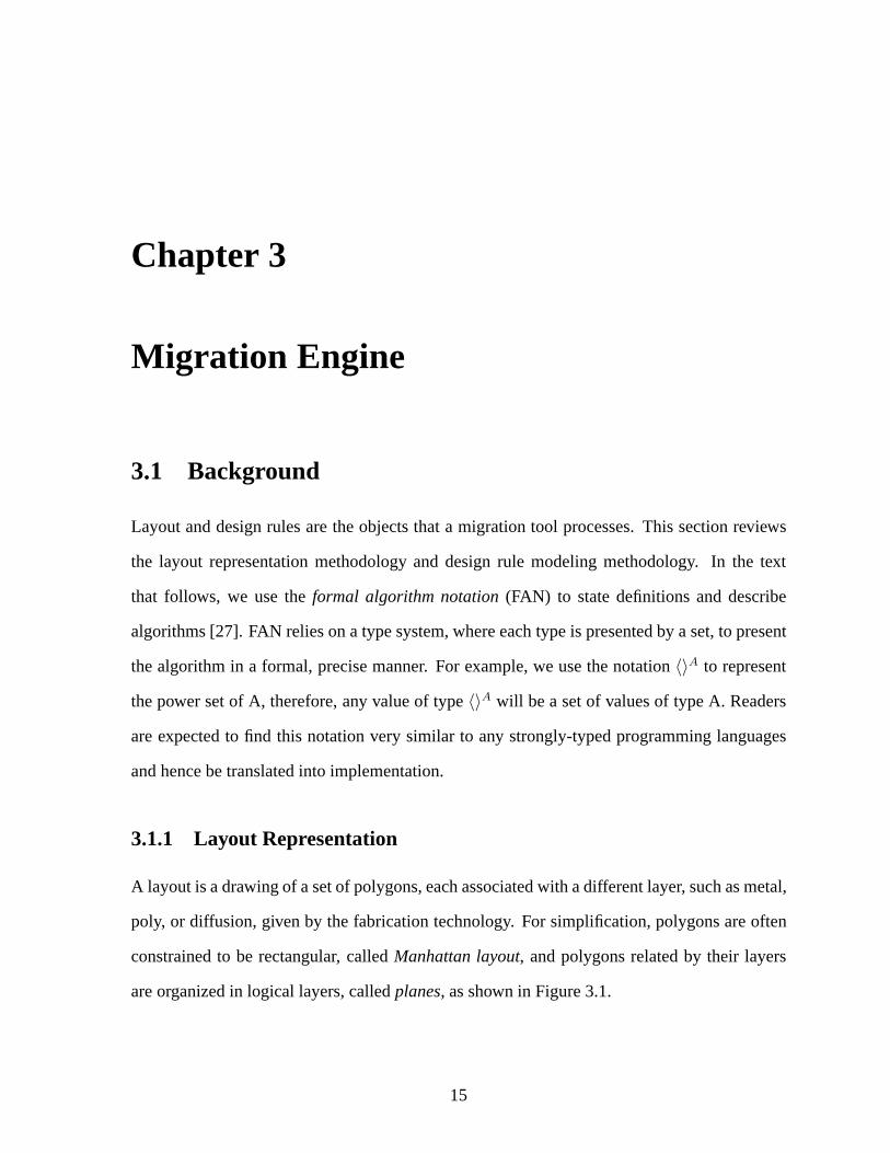
are organized in logical layers, calledplanes, as shown in Figure 3.1.
15

CHAPTER 3. MIGRATION ENGINE 16
3.1.2 Corner stitching
Metal1 plane
Active plane
Well plane
Figure 3.1: A layout is composed of several planes.
Choosing a good layout representation is a key to producing fast geometric operations for
migration tools. In this project, a data structure calledcorner stitchingwhich can provide fast
operations such as neighbor finding is used to represent the layout [19]. A brief discussion of
the corner stitching algorithm is given in this section.
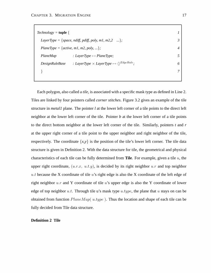
We first defineTechnologyand the data structure to represent it.
Definition 1 Technologydefines the information that are related to the fabrication technology.
It includesLayerType which is a set of mask types,PlaneTypewhich is a set of plane types
and a mapping from LayerType to PlaneTypePlaneMap which is used to identify the plane
that a polygon with certain mask type can stay on andDesignRuleBasewhich is used to store
all the design rules specified by fabrication technology and will be discussed in more detail in
Section 3.1.4.
CHAPTER 3. MIGRATION ENGINE 17
Technology =tuple { 1
LayerType ={space, ndiff, pdiff, poly, m1, m2,2 ...}; 3
PlaneType ={active, m1, m2, poly, ...}; 4
PlaneMap : LayerType7→ PlaneType; 5
DesignRuleBase : LayerType× LayerType7→ 〈〉EdgeRule; 6
} 7
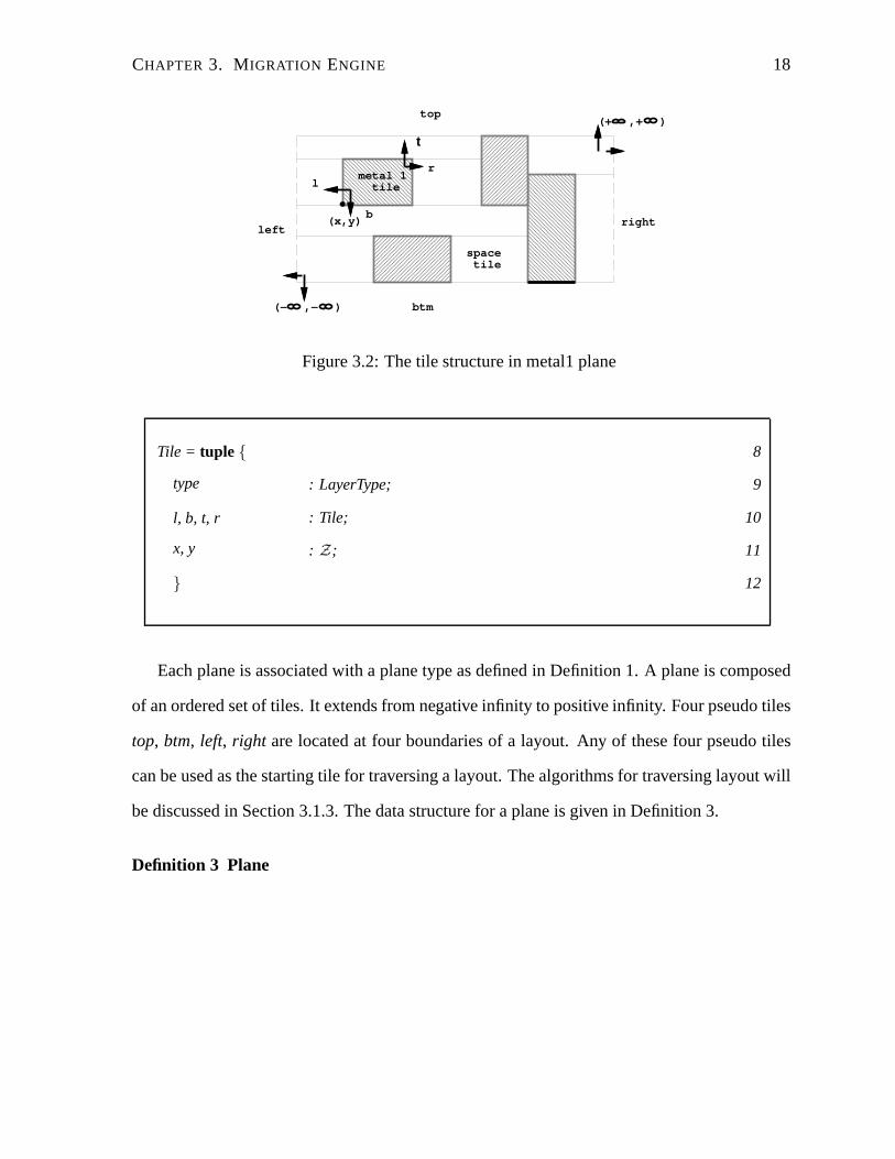
Each polygon, also called atile, is associated with a specific mask type as defined in Line 2.
Tiles are linked by four pointers calledcorner stitches. Figure 3.2 gives an example of the tile
structure inmetal1plane. The pointerl at the lower left corner of a tile points to the direct left
neighbor at the lower left corner of the tile. Pointerb at the lower left corner of a tile points
to the direct bottom neighbor at the lower left corner of the tile. Similarly, pointerst and r
at the upper right corner of a tile point to the upper neighbor and right neighbor of the tile,
respectively. The coordinate{x,y} is the position of the tile’s lower left corner. The tile data
structure is given in Definition 2. With the data structure for tile, the geometrical and physical
characteristics of each tile can be fully determined fromTile. For example, given a tileu, the
upper right coordinate,(u.r.x, u.t.y), is decided by its right neighboru.r and top neighbor
u.t because the X coordinate of tileu’s right edge is also the X coordinate of the left edge of
right neighboru.r and Y coordinate of tileu’s upper edge is also the Y coordinate of lower
edge of top neighboru.t. Through tile u’s mask typeu.type, the plane thatu stays on can be
obtained from functionP laneMap( u.type ). Thus the location and shape of each tile can be
fully decided from Tile data structure.
Definition 2 Tile
CHAPTER 3. MIGRATION ENGINE 18
space tile
metal 1 tile
(x,y)
r
l
b
(− ),−
),+(+top
btm
rightleft
t
Figure 3.2: The tile structure in metal1 plane
Tile = tuple { 8
type : LayerType; 9
l, b, t, r : Tile; 10
x, y : Z; 11
} 12
Each plane is associated with a plane type as defined in Definition 1. A plane is composed
of an ordered set of tiles. It extends from negative infinity to positive infinity. Four pseudo tiles
top, btm, left, right are located at four boundaries of a layout. Any of these four pseudo tiles
can be used as the starting tile for traversing a layout. The algorithms for traversing layout will
be discussed in Section 3.1.3. The data structure for a plane is given in Definition 3.
Definition 3 Plane
CHAPTER 3. MIGRATION ENGINE 19
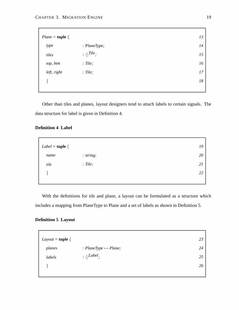
Plane = tuple { 13
type : PlaneType; 14
tiles : 〈〉Tile; 15
top, btm : Tile; 16
left, right : Tile; 17
} 18
Other than tiles and planes, layout designers tend to attach labels to certain signals. The
data structure for label is given in Definition 4.
Definition 4 Label
Label = tuple { 19
name : string; 20
tile : Tile; 21
} 22
With the definitions for tile and plane, a layout can be formulated as a structure which
includes a mapping from PlaneType to Plane and a set of labels as shown in Definition 5.
Definition 5 Layout
Layout = tuple { 23
planes : PlaneType7→ Plane; 24
labels : 〈〉Label; 25
} 26

CHAPTER 3. MIGRATION ENGINE 20
3.1.3 Algorithms
There are many algorithms used for processing tiles using corner stitching representation
methodology defined in the previous section, such as neighbor tile finding, locating and enu-
merating tiles, searching area, etc [19]. This section gives a discussion of three algorithms
often used in our migration engine.
Algorithm 1 Find all the right neighbor tiles of given a tiles.
rightNeighborFind =func( 27
pl : Plane, 28
s: Tile 29
) : [ ]T ile { 30
var nbr : Tile; 31
var nbrSet :[ ]T ile; 32
33
nbrSet =�; 34
nbr = ti.r; 35
if ( nbr 6= pl.right ) 36
do { 37
nbrSet = nbrSetcup {nbr}; 38
nbr = nbr.b; 39
} while( nbr.y> s.y ) 40
return nbrSet ; 41
} 42
Example 1
Figure 3.3 shows an example to demonstrate this algorithm. The searching prcoess is as fol-
lows:

CHAPTER 3. MIGRATION ENGINE 21
1. First, it visits the top right neighbor of tiles through itsr pointer. If s.r is not the right
pseudo tile, add it into the neighbor tiles set.
2. Check if the bottom edge of the neighbor tile is still above the bottom edge of tiles. If
this is true, move downward until it finds a tile whole bottom edge is lower than that of
s.
3. Otherwise, return the neighbor tiles set.
s
Figure 3.3: The process to find right neighor tiles.
Algorithm 2 Find the tile that contains a given (x,y) location on a given plane.
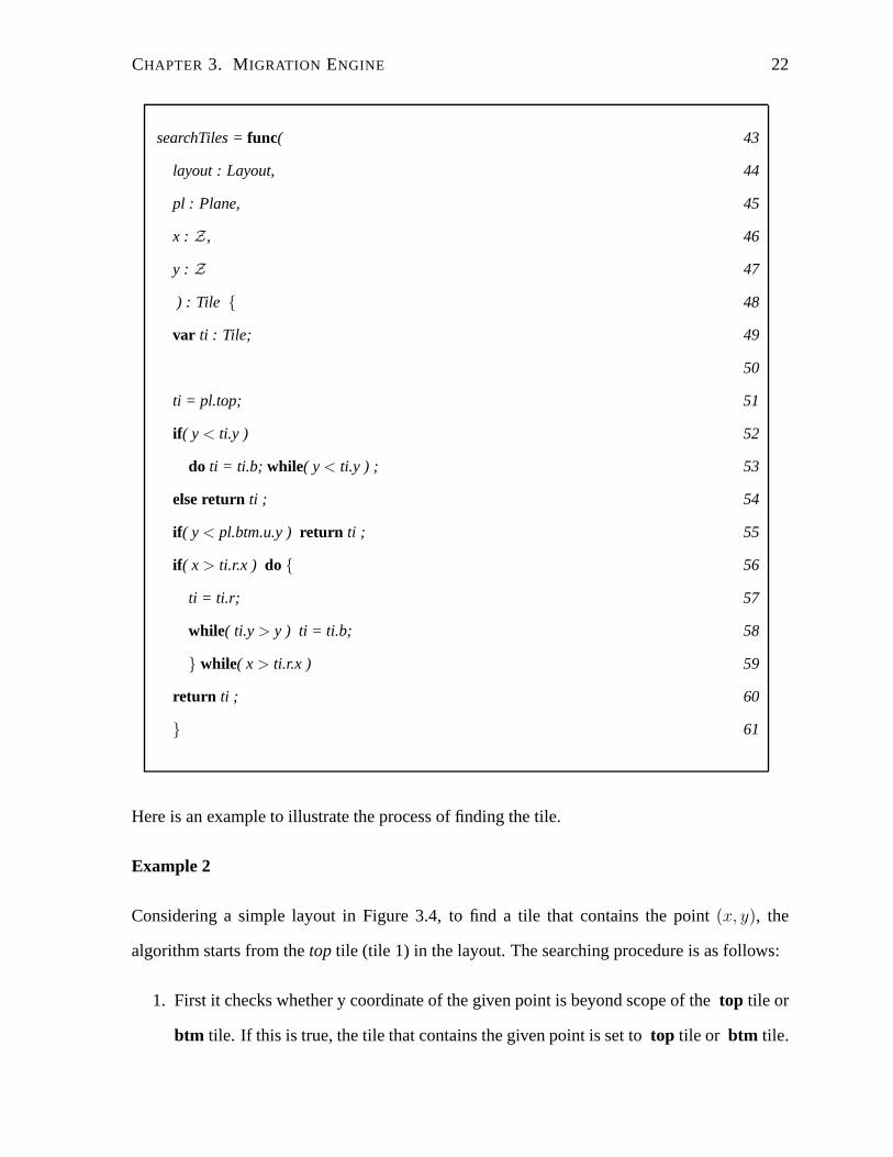
CHAPTER 3. MIGRATION ENGINE 22
searchTiles =func( 43
layout : Layout, 44
pl : Plane, 45
x : Z, 46
y : Z 47
) : Tile { 48
var ti : Tile; 49
50
ti = pl.top; 51
if ( y < ti.y ) 52
do ti = ti.b; while( y < ti.y ) ; 53
else return ti ; 54
if ( y < pl.btm.u.y ) return ti ; 55
if ( x > ti.r.x ) do { 56
ti = ti.r; 57
while( ti.y > y ) ti = ti.b; 58
} while( x > ti.r.x ) 59
return ti ; 60
} 61
Here is an example to illustrate the process of finding the tile.
Example 2
Considering a simple layout in Figure 3.4, to find a tile that contains the point(x, y), the
algorithm starts from thetop tile (tile 1) in the layout. The searching procedure is as follows:
1. First it checks whether y coordinate of the given point is beyond scope of thetop tile or
btm tile. If this is true, the tile that contains the given point is set totop tile or btm tile.

CHAPTER 3. MIGRATION ENGINE 23
2. Otherwise, the search moves downward, until it finds the tile whose vertical range covers
the desired point (For example, this occurs when tile 5 is found).
3. Select the right neighbor whose horizontal range contains the desired point and then trace
rightward( For example, tile 6 has three neighbors: tile 7, tile 8 and tile 9. The lower
bound of tile 7 and tile 8 is upper to the desired point, so it traces downward until tile 9 is
found and from tile 9, trace goes rightward). The rightward trace keeps on until it finds
the tile that contains the point ( tile 10 ).
1
2
3
4
5 6
7
8
9 10
pl.top
pl.btm
(x,y)
Figure 3.4: The process to locate the tile that contains a given point
Algorithm 3 Enumerate all tiles on a given plane. In this algorithm, each tile is visited only
after all tiles above it and to its left have been visited.
CHAPTER 3. MIGRATION ENGINE 24
enumerateTiles =func( pl : Plane ) : [ ]T ile { 62
var tiles : [ ]T ile; 63
var start : Tile; 64
65
tiles = �; 66
start = pl.top.b; 67
while( start.b 6= pl.btm ) { 68
tiles = eachTile( pl,tiles, start ) ; 69
start = start.b; 70
} 71
return tiles ; 72
} 73
74
eachTile =func( 75
pl : Plane, tiles:[ ]T ile, ti: Tile 76
) : [ ]T ile { 77
var right : Tile; 78
79
tiles = tiles∪ {ti}; 80
if ( ti.r == NULL ) ; return tiles ; 81
else{ 82
right = ti.r; 83
while( right.y >= ti.y ) { 84
tiles = eachTile( pl, tiles, right); 85
right = right.b; 86
} 87
} 88
} 89
90
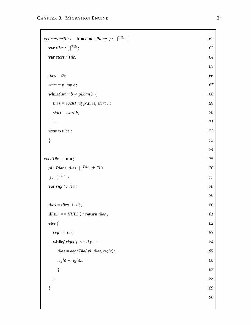
CHAPTER 3. MIGRATION ENGINE 25
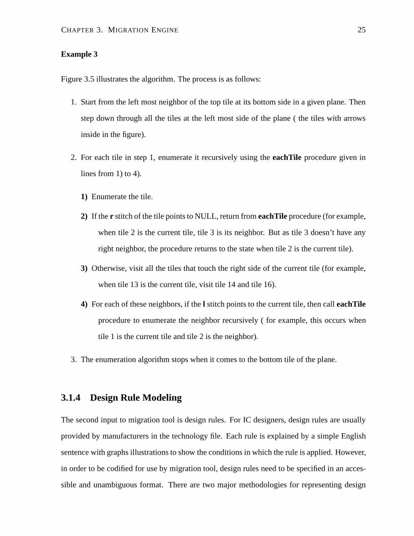
Example 3
Figure 3.5 illustrates the algorithm. The process is as follows:
1. Start from the left most neighbor of the top tile at its bottom side in a given plane. Then
step down through all the tiles at the left most side of the plane ( the tiles with arrows
inside in the figure).
2. For each tile in step 1, enumerate it recursively using theeachTile procedure given in
lines from 1) to 4).
1) Enumerate the tile.
2) If the r stitch of the tile points to NULL, return fromeachTileprocedure (for example,
when tile 2 is the current tile, tile 3 is its neighbor. But as tile 3 doesn’t have any
right neighbor, the procedure returns to the state when tile 2 is the current tile).
3) Otherwise, visit all the tiles that touch the right side of the current tile (for example,
when tile 13 is the current tile, visit tile 14 and tile 16).
4) For each of these neighbors, if thel stitch points to the current tile, then calleachTile
procedure to enumerate the neighbor recursively ( for example, this occurs when
tile 1 is the current tile and tile 2 is the neighbor).
3. The enumeration algorithm stops when it comes to the bottom tile of the plane.
3.1.4 Design Rule Modeling
The second input to migration tool is design rules. For IC designers, design rules are usually
provided by manufacturers in the technology file. Each rule is explained by a simple English
sentence with graphs illustrations to show the conditions in which the rule is applied. However,
in order to be codified for use by migration tool, design rules need to be specified in an acces-
sible and unambiguous format. There are two major methodologies for representing design

CHAPTER 3. MIGRATION ENGINE 26
1 2
3
4
56
7
8
9 10 11
12 1314 15
16
top
btm
Figure 3.5: Tile enumeration.
rules. One is calledmask-baseddesign rule which is the basis of commercial design rule check
packageDracula [2]; the other is callededge-baseddesign rule model which is the basis of
layout edit tool Magic [2]. In this project, theedge-baseddesign rule model is used because
of its ability to translate the high level design rules such as minimum spacing rule, minimum
width rule, etc, into a set of edge rules and thus we can represent the design rules as constraints
between individual edges. This section will briefly introduce this model and its data structure.
For detailed discussion, please refer to [24].
type2 type1type2type1
type1
type2
type1
type2
Figure 3.6: Each edge rule can be applied in any of the four directions.
The edge rule is applied on an edge between two tiles of different LayerType in any of
four directions as shown by arrows in Figure 3.6. Without loss of generality, in the following
discussion, we assume that the edge rule is applied towards the east. A distancedistand certain
mask layers calledokTypesarea are specified so that only tiles ofokTypesare permitted within
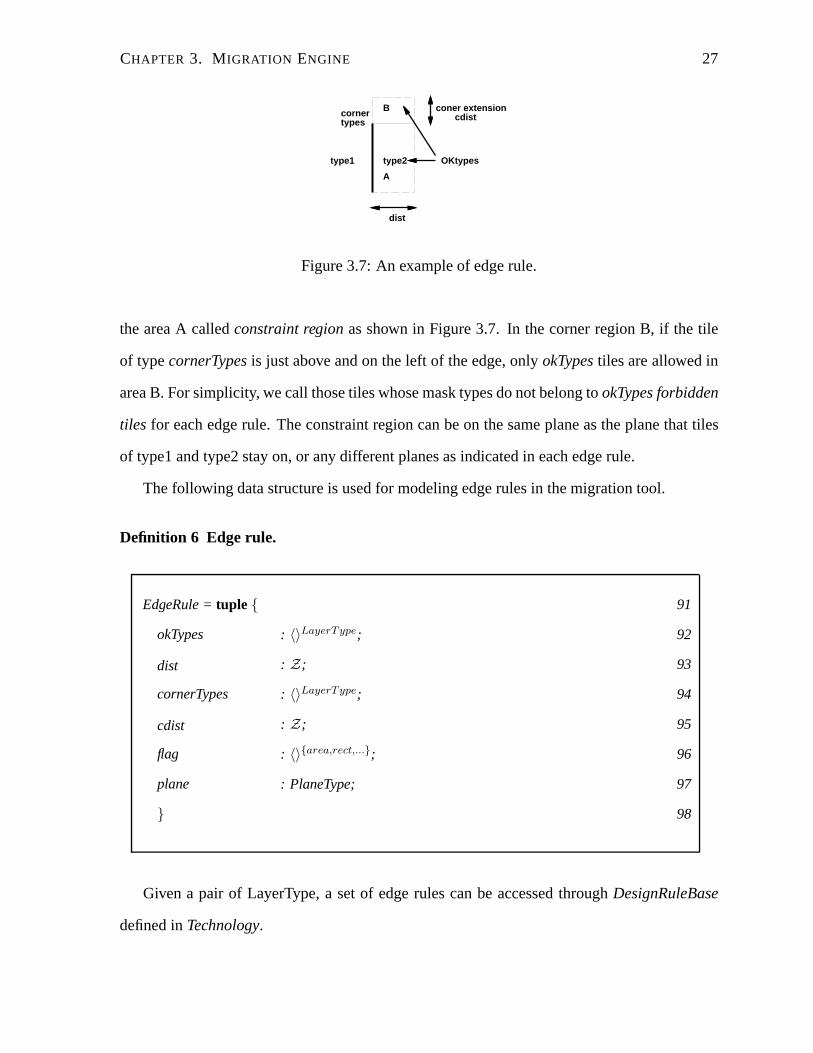
CHAPTER 3. MIGRATION ENGINE 27
type1 type2
coner extension
OKtypes
A
Bcornertype
dist
cdists
Figure 3.7: An example of edge rule.
the area A calledconstraint regionas shown in Figure 3.7. In the corner region B, if the tile
of typecornerTypesis just above and on the left of the edge, onlyokTypestiles are allowed in
area B. For simplicity, we call those tiles whose mask types do not belong tookTypes forbidden
tiles for each edge rule. The constraint region can be on the same plane as the plane that tiles
of type1 and type2 stay on, or any different planes as indicated in each edge rule.
The following data structure is used for modeling edge rules in the migration tool.
Definition 6 Edge rule.
EdgeRule =tuple { 91
okTypes : 〈〉LayerType; 92
dist : Z; 93
cornerTypes : 〈〉LayerType; 94
cdist : Z; 95
flag : 〈〉{area,rect,...}; 96
plane : PlaneType; 97
} 98
Given a pair of LayerType, a set of edge rules can be accessed throughDesignRuleBase
defined inTechnology.

CHAPTER 3. MIGRATION ENGINE 28
3.2 Migration Engine
As the layout is composed of a set of tiles, the migration engine can generate a new layout by
determining new positions of horizontal and vertical edges of all tiles. It employs the traditional
1-D compaction strategy by first migrating along the X direction, i.e. determining positions of
vertical edges, and then the Y direction. Without loss of generality, in the discussion that
follows, we assume migration in the X direction only.
The basic strategy for migration is to abstract all the requirements or constraints among
all the edges in a layout, such as design rules and other practical consideration. And then
with respect to all these constraints, new edge positions are decided under certain optimization
goal. With the corner stitching data structure discussed in Chapter 2, tile shapes and design
rules are specified in the Mead and Conway’sλ based methodology [16], which means that
the positions of tiles are all specified in terms ofλ. Take the layout in Figure 3.8, tiles are all
aligned in grids whose minimum spacing is1λ, which implies that the coordinates of all edges
are integers. At the same time, design rules are specified in terms ofλ also. And all design rules
can be expressed as inequalities when they are applied to the layout. For example, suppose the
minimum width requirement for tile 1 is4λ in Figure 3.8 and this rule can be translated into an
inequality as:
x2 − x1 ≥ 4 (3.1)
Thus, the layout migration problem can be formulated as an integer linear programming
(ILP) problem:
minimize oT x
subject to Ax ≥ b
x ≥ 0
Herex is a vector of variables to be determined, and in the simplest case would just be

CHAPTER 3. MIGRATION ENGINE 29
x x
x x
1 2
3 4
1
2
Figure 3.8: Tiles are aligned in grids
coordinates for all vertical edges. In this project,x is a vector of coordinates for all tiles’ left
vertical edges. Vectorso represent the coefficients ofx in the objective function of optimiza-
tion. Each row of arrayA represents coefficients ofx in an inequality. We call this type of
migration asconstraint-based migration.
Suppose we want to migrate the layout in Figure 3.8 so that the new layout does not have
design rule violations and the layout area is minimum. For simplicity, we only consider the
minimum width rule and minimum spacing rule for tile 1 and tile 2. The minimum width for
tile 1 and tile is4λ and minimum distance between tile 1 and tile 2 is3λ. This problem is
formulated as:
minimize x4 − x1
subject to x2 − x1 ≥ 4
x4 − x3 ≥ 4
x3 − x2 ≥ 3
x1 ≥ 0
x2 ≥ 0
x3 ≥ 0
x4 ≥ 0
After solving this ILP problem, we can get the value for eachx, and new positions of each
CHAPTER 3. MIGRATION ENGINE 30
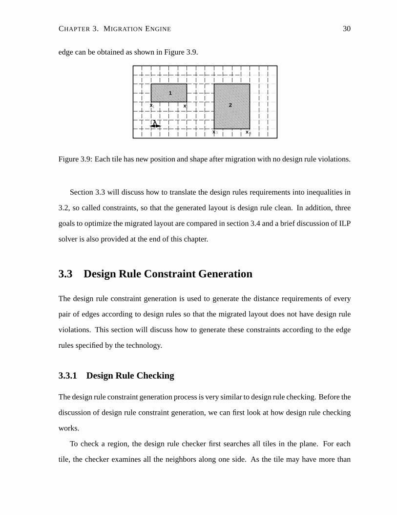
edge can be obtained as shown in Figure 3.9.
x x1 2
x3 x 4
1
2
Figure 3.9: Each tile has new position and shape after migration with no design rule violations.
Section 3.3 will discuss how to translate the design rules requirements into inequalities in
3.2, so called constraints, so that the generated layout is design rule clean. In addition, three
goals to optimize the migrated layout are compared in section 3.4 and a brief discussion of ILP
solver is also provided at the end of this chapter.
3.3 Design Rule Constraint Generation
The design rule constraint generation is used to generate the distance requirements of every
pair of edges according to design rules so that the migrated layout does not have design rule
violations. This section will discuss how to generate these constraints according to the edge
rules specified by the technology.
3.3.1 Design Rule Checking
The design rule constraint generation process is very similar to design rule checking. Before the
discussion of design rule constraint generation, we can first look at how design rule checking
works.
To check a region, the design rule checker first searches all tiles in the plane. For each
tile, the checker examines all the neighbors along one side. As the tile may have more than
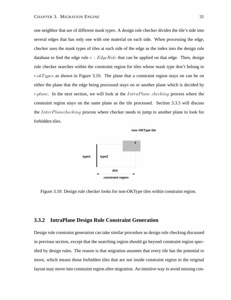
CHAPTER 3. MIGRATION ENGINE 31
one neighbor that are of different mask types. A design rule checker divides the tile’s side into
several edges that has only one with one material on each side. When processing the edge,
checker uses the mask types of tiles at each side of the edge as the index into the design rule
database to find the edge ruler : EdgeRule that can be applied on that edge. Then, design
rule checker searches within the constraint region for tiles whose mask type don’t belong to
r.okTypes as shown in Figure 3.10. The plane that a constraint region stays on can be on
either the plane that the edge being processed stays on or another plane which is decided by
r.plane. In the next section, we will look at theIntraP lane checking process where the
constraint region stays on the same plane as the tile processed. Section 3.3.5 will discuss
the InterP lanechecking process where checker needs to jump to another plane to look for
forbidden tiles.
type1 type2
constraint region
dist
non−OKType tile
Figure 3.10: Design rule checker looks for non-OKType tiles within constraint region.
3.3.2 IntraPlane Design Rule Constraint Generation
Design rule constraint generation can take similar procedure as design rule checking discussed
in previous section, except that the searching region should go beyond constraint region spec-
ified by design rules. The reason is that migration assumes that every tile has the potential to
move, which means those forbidden tiles that are not inside constraint region in the original
layout may move into constraint region after migration. An intuitive way to avoid missing con-

CHAPTER 3. MIGRATION ENGINE 32
straints is to extend the constraint region to the boundary of layout as the checking region in
Figure 3.11(a) and generate constraints between all necessary pair of edges. Take poly spacing
rule as an example, the TSMC 0.25um technology specifies that the spacing of poly should be
greater than 3λ, which can be translated into edge rule as the following:
edgepoly poly 3 poly 3
1 23
4 5
6 7 8
2
3 4 5
87
33
3
(a) (b)
9 109 10
3
checking region
Figure 3.11: (a) An example layout in active plane. The shaded rectangles 1, 3, 5, 6 and 10
represent poly tiles. Rectangle 8 is diffusion tile. Other rectangles are all space tiles. (b) The
constraint graph generated from poly spacing rule.
Given a simple layout as Figure 3.11(a), according to this rule, four constraints need to be
generated to guarantee enough spacing between poly when processing the edge between tile 1
and tile 2 (corner region checking is not considered at this moment). They are:
• x3 − x2 ≥ 3 The left edge of tile 3 should be at least 3λ away from left edge of tile 2.
• x5 − x2 ≥ 3 The left edge of tile 5 should be at least 3λ away from left edge of tile 2.
• x5 − x3 ≥ 3 The left edge of tile 5 should be at least 3λ away from left edge of tile 3.
• x10 − x7 ≥ 3 The left edge of tile 10 should be at least 3λ away from left edge of tile 7.
These constraints can be visualized using a directed graphG = 〈V, E〉 as shown in Fig-
ure 3.11(b). Each vertex represents the X coordinate of a tile’s left edge. For each inequality
of the formxj − xi ≥ dij , there is an arc〈vi, vj〉 with weightdij .

CHAPTER 3. MIGRATION ENGINE 33
Note that with constraint-based migration methodology, the width and height of tiles may
be changed after migration in order to satisfy the constraints. However, migration must main-
tain that the given circuit topology keep the same functionality of the circuit, i.e., the corner
stitching representation of the layout is kept unchanged. So after migration, the four pointers
of each tile must point to the same tiles as in the old layout. The relative position of tiles are
not changed. For example, the tile 5 in Figure 3.11 is on the right side of tile 3 in the old layout
and after migration tile 5 cannot move to the left side of tile 3. Therefore, the arc〈v2, v5〉 in
Figure 3.11(b) is redundant because the tile 5 is always on the right side of tile 3 and the dis-
tance constraint between left edge of tile 2 and tile 3 ( arc〈v2, v3〉 ) guarantees that the distance
between left edge of tile 2 and tile 5 cannot be less than3λ. In other words, if an edge of
forbidden tile (tile 5) stays behind another forbidden tile (tile 3), it will not generate constraint
between the edge that is being processed and the edge in the “shadow” of forbidden tiles.
Another redundant arc in Figure 3.11(b) is arc〈v7, v10〉. As discussed before, the tile struc-
ture will not be changed after migration, which implies that tiles cannot be eliminated after
migration. We can assume that the minimum tile width should be greater than or equal to1λ.
So the minimum separation between the left edge of tile 7 and tile 10 should be greater or equal
than the sum of minimum width requirement of tile 7, 8 and 9, which is greater than or equal
to the minimum spacing3λ. This makes the arc〈v7, v10〉 redundant for migration.
A new design rule constraint generation methodDepth-K searchingalgorithm is proposed
in this project which greatly reduces the checking region and reduces the redundant constraints.
A detailed discussion of this algorithm follows.
3.3.3 The Depth-K searching algorithm
To gain more insight into the problem, we first build a graphshadowing neighborhood graph
that captures the neighboring relation. As we can observe from Figure 3.11 that constraints
should be generated only for tiles that overlap with the checking edge vertically, ashadowing
neighborhood graphdefined in Definition 7 is used to limit the searching space.
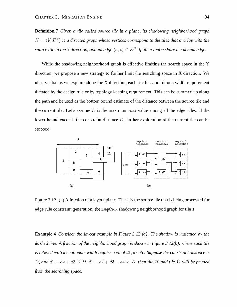
CHAPTER 3. MIGRATION ENGINE 34
Definition 7 Given a tile called source tile in a plane, its shadowing neighborhood graph
N = 〈V, EN〉 is a directed graph whose vertices correspond to the tiles that overlap with the
source tile in the Y direction, and an edge〈u, v〉 ∈ EN iff tile u andv share a common edge.
While the shadowing neighborhood graph is effective limiting the search space in the Y
direction, we propose a new strategy to further limit the searching space in X direction. We
observe that as we explore along the X direction, each tile has a minimum width requirement
dictated by the design rule or by topology keeping requirement. This can be summed up along
the path and be used as the bottom bound estimate of the distance between the source tile and
the current tile. Let’s assumeD is the maximumdist value among all the edge rules. If the
lower bound exceeds the constraint distanceD, further exploration of the current tile can be
stopped.
1
23 4
5
67
8
9
D
1 d1
2 d2
3 d3
8 d8
9 d9 7 d7
4 d4
5 d5
6 d6
(a) (b)
10
11
Depth 1neighbor
Depth 2neighbor
Depth 3neighbor
Figure 3.12: (a) A fraction of a layout plane. Tile 1 is the source tile that is being processed for
edge rule constraint generation. (b) Depth-K shadowing neighborhood graph for tile 1.
Example 4 Consider the layout example in Figure 3.12 (a). The shadow is indicated by the
dashed line. A fraction of the neighborhood graph is shown in Figure 3.12(b), where each tile
is labeled with its minimum width requirement ofd1, d2 etc. Suppose the constraint distance is
D, andd1 + d2 + d3 ≤ D, d1 + d2 + d3 + d4 ≥ D, then tile 10 and tile 11 will be pruned
from the searching space.
CHAPTER 3. MIGRATION ENGINE 35
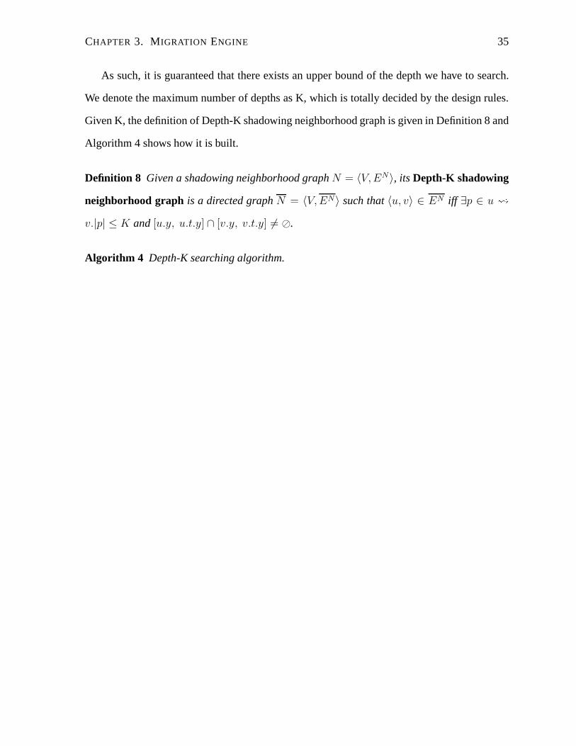
As such, it is guaranteed that there exists an upper bound of the depth we have to search.
We denote the maximum number of depths as K, which is totally decided by the design rules.
Given K, the definition of Depth-K shadowing neighborhood graph is given in Definition 8 and
Algorithm 4 shows how it is built.
Definition 8 Given a shadowing neighborhood graphN = 〈V, EN〉, its Depth-K shadowing
neighborhood graph is a directed graphN = 〈V, EN〉 such that〈u, v〉 ∈ EN iff ∃p ∈ u
v.|p| ≤ K and[u.y, u.t.y] ∩ [v.y, v.t.y] 6= �.
Algorithm 4 Depth-K searching algorithm.
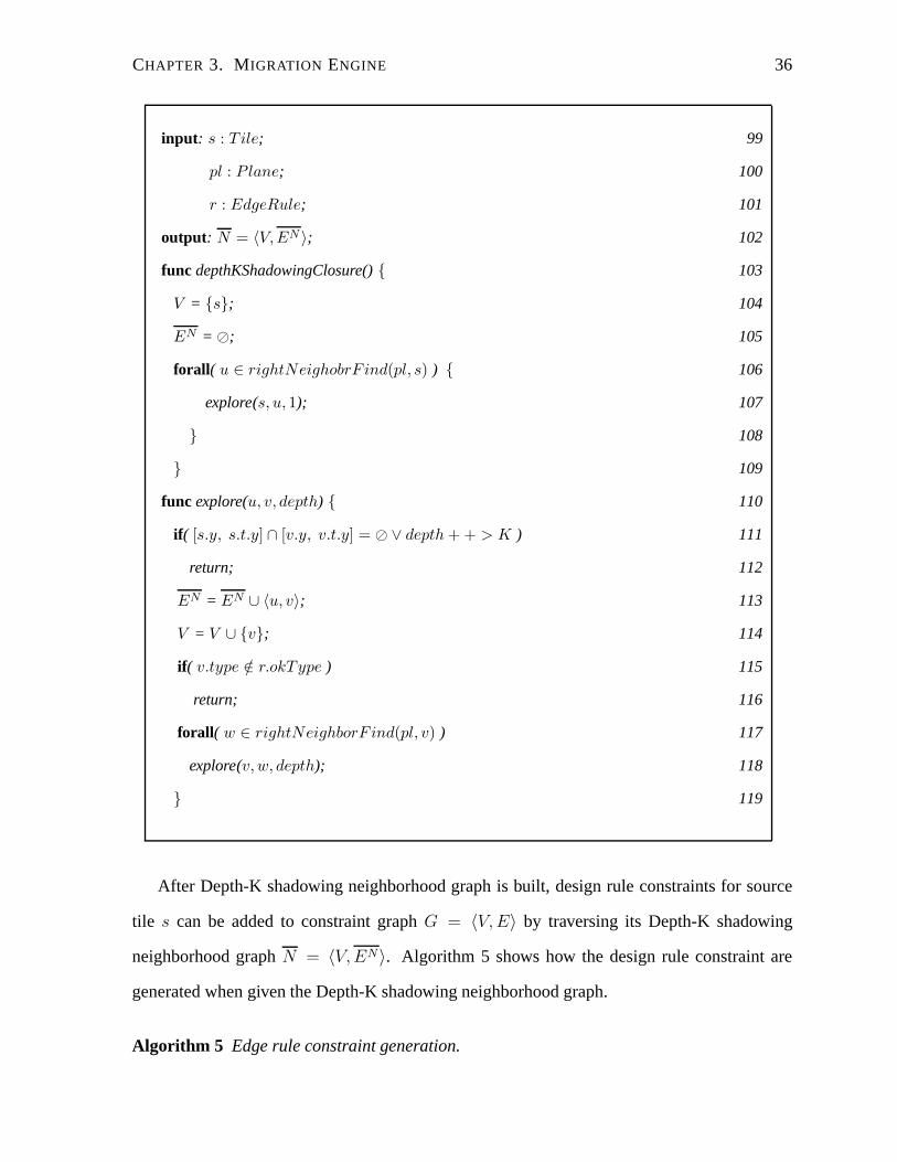
CHAPTER 3. MIGRATION ENGINE 36
input : s : T ile; 99
pl : Plane; 100
r : EdgeRule; 101
output: N = 〈V,EN 〉; 102
func depthKShadowingClosure(){ 103
V = {s}; 104
EN = �; 105
forall ( u ∈ rightNeighobrF ind(pl, s) ) { 106
explore(s, u, 1); 107
} 108
} 109
func explore(u, v, depth) { 110
if ( [s.y, s.t.y] ∩ [v.y, v.t.y] = � ∨ depth + + > K ) 111
return; 112
EN = EN ∪ 〈u, v〉; 113
V = V ∪ {v}; 114
if ( v.type /∈ r.okType ) 115
return; 116
forall ( w ∈ rightNeighborF ind(pl, v) ) 117
explore(v,w, depth); 118
} 119
After Depth-K shadowing neighborhood graph is built, design rule constraints for source
tile s can be added to constraint graphG = 〈V, E〉 by traversing its Depth-K shadowing
neighborhood graphN = 〈V, EN〉. Algorithm 5 shows how the design rule constraint are
generated when given the Depth-K shadowing neighborhood graph.
Algorithm 5 Edge rule constraint generation.
CHAPTER 3. MIGRATION ENGINE 37
input : s : T ile; 120
N = 〈V,EN 〉; 121
R : EdgeRule; 122
output: G = 〈V,E〉; 123
func addEdgeConstraints(){ 124
forall ( u ∈ V ) 125
if ( u.type /∈ R.OKType ) { 126
E = E ∪ 〈s, u〉; 127
weight(〈s, u〉) = R.dist; 128
} 129
} 130
131
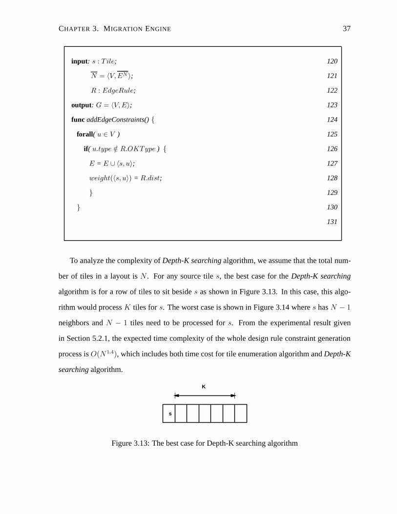
To analyze the complexity ofDepth-K searchingalgorithm, we assume that the total num-
ber of tiles in a layout isN . For any source tiles, the best case for theDepth-K searching
algorithm is for a row of tiles to sit besides as shown in Figure 3.13. In this case, this algo-
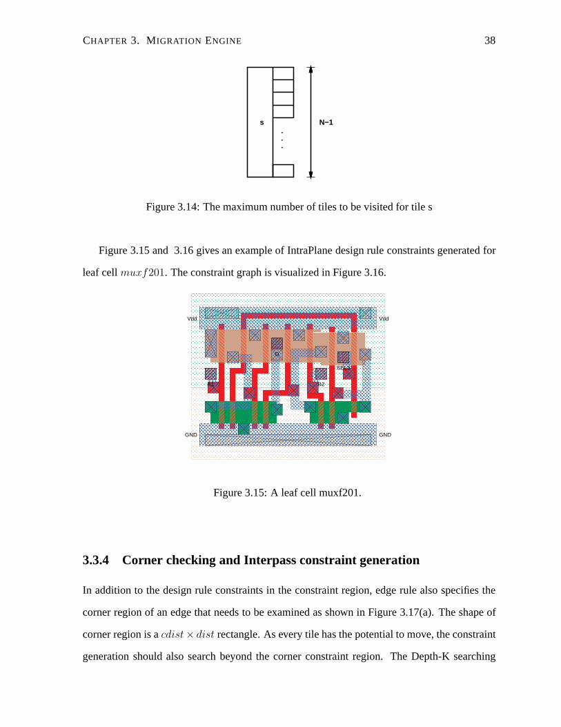
rithm would processK tiles for s. The worst case is shown in Figure 3.14 wheres hasN − 1
neighbors andN − 1 tiles need to be processed fors. From the experimental result given
in Section 5.2.1, the expected time complexity of the whole design rule constraint generation
process isO(N1.4), which includes both time cost for tile enumeration algorithm andDepth-K
searchingalgorithm.
s
K
Figure 3.13: The best case for Depth-K searching algorithm
CHAPTER 3. MIGRATION ENGINE 38
.
.
.
s N−1
Figure 3.14: The maximum number of tiles to be visited for tile s
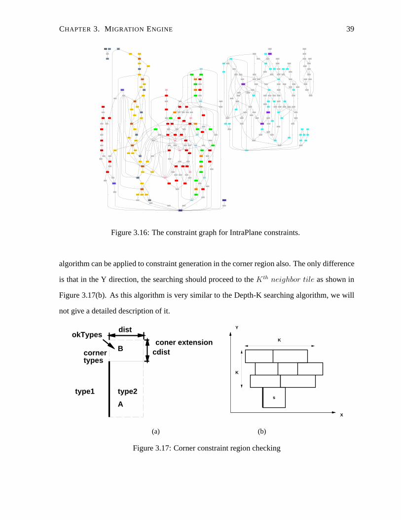
Figure 3.15 and 3.16 gives an example of IntraPlane design rule constraints generated for
leaf cellmuxf201. The constraint graph is visualized in Figure 3.16.
��������������������������������������������������������������������������������������������������������������������������������������������������������������������������������������������������������������������������������������������������������������������������������������������������������������������������������������������������������������������������������������������������������
��������������������������������������������������������������������������������������������������������������������������������������������������������������������������������������������������������������������������������������������������������������������������������������������������������������������
���������
����
��������
������������
��������������
������
������
������
������������
���������
���������
������
���������
���������������
����
����������������
������������
������������������������
����������������
������������
��������������������
������
������������
�����������������
������
������
����
������������
������
������
������������
������������
����������
����������
��������
��������
��������
����
����
��������
������
����������������������������������
����
��
��
����
����
�� ����
����
������������
��
��
������
����������
������
��������� ��
������
��������
��
���������
������� ��
������
����
������
� ����������������
�� ��������
����
����
����
������
������
������������
������
������
������������
������������
����������
����������
��������
��������
��������
����
����
��������
������
���������������������������������������������������������������������������
������������������
���������
Vdd
GND
Vdd
GND
O
SEL3
A1 B2
Figure 3.15: A leaf cell muxf201.
3.3.4 Corner checking and Interpass constraint generation
In addition to the design rule constraints in the constraint region, edge rule also specifies the
corner region of an edge that needs to be examined as shown in Figure 3.17(a). The shape of
corner region is acdist× dist rectangle. As every tile has the potential to move, the constraint
generation should also search beyond the corner constraint region. The Depth-K searching
CHAPTER 3. MIGRATION ENGINE 39
nwell:7
space:9
12
pwell:8
1
pwell:8
12
psubc:15
space:16
3
space:17
3
psubc:20
4
pfet:105
4
pfet:100
4
pfet:62
4
pfet:57
4
pfet:51
4
poly:18
1
space:21
3
pdiff:106
2
pdiff:108
2
pdiff:111
2
pdiff:101
2
pdiff:104
2
pdiff:63
2
pdiff:69
2
pdiff:70
2
pdiff:73
2
pdiff:58
2
pdiff:61
2
pdiff:52
2
pdiff:53
2
pdiff:56
2
space:19
2
space:27
2
1
poly:67
3
psubc:199
1
poly:24
space:25
2
poly:26
3
2
space:28
2
poly:29
3
2
2
space:68
2
space:30
2
poly:31
3
space:32
2
poly:33
3
space:34
2
space:35
2
3
poly:65
3
space:66
2
pdc:37
pdiff:38
1
space:112
3
pfet:41
1
1
pdiff:42
2
pdiff:43
2
pdiff:40
4
pfet:46
4
pdc:44
1
pdiff:47
2
pdiff:50
2
pdiff:45
1
1
pc:127
2
pdc:59
1
pdc:102
1
poly:128
1
pdiff:60
1
pdiff:103
1
pdc:48
1
4
pdiff:49
1
1
pdc:71
1
pdc:54
1
pdiff:72
1
pdiff:55
14
1
4
1
2
1
1
1
4
1
1
space:64
4
4
1
41
3
1
1
21
pc:76
poly:78
1
4
space:79
2
space:83
2
poly:80
3
poly:84
3
poly:88
3
space:81
2
poly:82
3
poly:86
3
space:87
2 2
space:94
2
poly:95
3
poly:114
1
pc:119
4
pc:121
4
space:85
2
space:89
2
space:91
2
space:115
2
3 poly:90
1
2
3 3
poly:118
3
space:96
2
1
space:120
1
space:122
2
4
pc:92
4
poly:116
3
poly:93
1
1
1
space:117
1
ndc:172
2
poly:177
4
ndc:160
2 ndc:158
2
3
poly:130
3
space:173
1
space:178
2
ndiff:161
1
nfet:166
3
space:176
3
space:159
1
space:162
12
4
poly:97
4
space:98
2
space:113
2
pdiff:99
1
poly:123
3
4
31
4
1
pdc:109
1
space:110
1space:107
4 14
1
1
space:124
2
space:126
2
space:129
2
2
space:131
2
space:133
2
4
44
poly:132
4
space:135
2
4
2
4
poly:136
4
pc:137
1
poly:125
4
4
poly:141
3
space:142
2
1
1 2
3
poly:134
3
3
4poly:139
3
2
space:138
1space:140
2
2
4
4
ndc:144
ndiff:145
1
space:164
3
space:187
3
nfet:148
1
ndc:186
1
ndiff:165
4
4
1
nfet:152
1
ndc:175
1
4
poly:188
1
ndiff:149
2
3
3 space:197
3
ndiff:147
3
3
4
nfet:150
4
ndiff:151
2
3
1
4
ndiff:153
2
4
nfet:154
4
ndiff:155
2
ndiff:157
2
ndiff:163
2
4
1
space:156
4 1 4
12
1
1
4
12
1212
4
12
12
4
1
1
ndiff:167
2
1
1
nfet:170
1
1
space:179
1
4
nfet:168
4
ndiff:169
2 ndiff:174
2
4
1
ndiff:171
2
1
1
1
1
poly:181
space:182
2
poly:183
3
space:184
2
1
1
space:189
2
poly:190
3
space:191
2
4
poly:192
3
space:193
2
poly:194
3
space:195
2
1
space:196
1
psubc:199
space:200
3
1
m1:204
m1:206
1
space:227
3
space:223
3
space:215
3
space:213
3
m1:206
4
m1:318
1
space:306
3
space:252
1 m1:224
3
space:252
3
space:252
3
1 space:223
3
m1:248
3
space:263
3
1
space:216
3
1
m1:208
4
space:210
1
1
m1:209
3
space:230
4
space:218
4
space:230
4
3
space:219
3
m1:234
3
4
space:216
4
space:217
1
4
3
space:263
3
space:247
4
via12:220
1
space:221
5
space:225
5
space:228
5
space:229
5
1 3
m1:264
3
3 3
3
via12:267
3
3
1
3
space:306
4
m1:268
5
3
4
space:250
4
space:251
4
space:252
4
space:233
4
m1:234
4
3 space:245
1
3
m1:262
3
space:237
via12:238
1
space:241
5
1
3
3
m1:244
3
m1:240
3
3
space:261
3
space:243
space:243
4
3
space:256
3
space:256
4
3
space:307
3
3
space:282
3
space:288
3
3
3
space:265
3
space:271
3
space:274
3
space:284
3
1
1
3
3
space:253
1
1
3
m1:257
3
space:297
m1:260
4
space:297
4
1
3
space:300
4
space:302
4
space:307
4
space:290
3
m1:289
3
m1:301
3
space:266
1
m1:272
3
m1:275
3
m1:281
3
space:287
3
1
space:269
1
space:273
1
3
m1:293
3
1
3
3
m1:276
1
space:286
3
via12:277
1
space:278
5
3
space:280
3
space:280
4
3
3
m1:294
3
4
space:290
4
3
space:310
3
4
space:287
4
3
space:292
4 m1:294
4
3
space:295
3
space:304
1
m1:296
3
space:310
4
3 1
3
3
3
3
space:304
4
3 3
3
space:310
3
4 1
3
m1:312
m1:315
1
m1:314
1
m1:315
41
space:319
1
1
m1:316
m1:318
1
m1:318
4
1
space:323
space:335
1
space:325
5
space:338
1
space:338
4
space:338
4
space:330
5
space:338
5
space:328
1
1
space:333
space:335
1
space:335
5
4
4
space:336
1
1
1
4
Figure 3.16: The constraint graph for IntraPlane constraints.
algorithm can be applied to constraint generation in the corner region also. The only difference
is that in the Y direction, the searching should proceed to theKth neighbor tile as shown in
Figure 3.17(b). As this algorithm is very similar to the Depth-K searching algorithm, we will
not give a detailed description of it.
type1 type2
coner extension
A
Bcornertype
dist
cdists
okTypes
s
K
K
X
Y
(a) (b)
Figure 3.17: Corner constraint region checking
CHAPTER 3. MIGRATION ENGINE 40
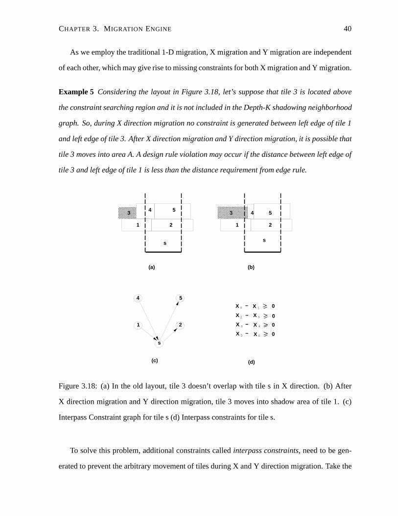
As we employ the traditional 1-D migration, X migration and Y migration are independent
of each other, which may give rise to missing constraints for both X migration and Y migration.
Example 5 Considering the layout in Figure 3.18, let’s suppose that tile 3 is located above
the constraint searching region and it is not included in the Depth-K shadowing neighborhood
graph. So, during X direction migration no constraint is generated between left edge of tile 1
and left edge of tile 3. After X direction migration and Y direction migration, it is possible that
tile 3 moves into area A. A design rule violation may occur if the distance between left edge of
tile 3 and left edge of tile 1 is less than the distance requirement from edge rule.
s
1 2
3 4 5
s
1 2
3 4 5
(a) (b)
s
1 2
4
(c)
0
0
0
0
X X 1
2
4
5
s −
X X
5
− s
X s − X
X − X s
(d)
Figure 3.18: (a) In the old layout, tile 3 doesn’t overlap with tile s in X direction. (b) After
X direction migration and Y direction migration, tile 3 moves into shadow area of tile 1. (c)
Interpass Constraint graph for tile s (d) Interpass constraints for tile s.
To solve this problem, additional constraints calledinterpass constraints, need to be gen-
erated to prevent the arbitrary movement of tiles during X and Y direction migration. Take the
CHAPTER 3. MIGRATION ENGINE 41
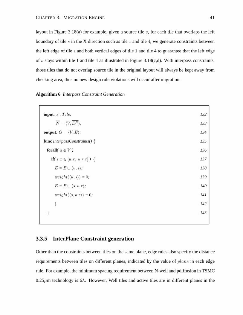
layout in Figure 3.18(a) for example, given a source tiles, for each tile that overlaps the left
boundary of tiles in the X direction such as tile1 and tile4, we generate constraints between
the left edge of tiles and both vertical edges of tile 1 and tile 4 to guarantee that the left edge
of s stays within tile1 and tile4 as illustrated in Figure 3.18(c,d). With interpass constraints,
those tiles that do not overlap source tile in the original layout will always be kept away from
checking area, thus no new design rule violations will occur after migration.
Algorithm 6 Interpass Constraint Generation
input : s : T ile; 132
N = 〈V,EN 〉; 133
output: G = 〈V,E〉; 134
func InterpassConstraints(){ 135
forall ( u ∈ V ) 136
if ( s.x ∈ [u.x, u.r.x] ) { 137
E = E ∪ 〈u, s〉; 138
weight(〈u, s〉) = 0; 139
E = E ∪ 〈s, u.r〉; 140
weight(〈s, u.r〉) = 0; 141
} 142
} 143
3.3.5 InterPlane Constraint generation
Other than the constraints between tiles on the same plane, edge rules also specify the distance
requirements between tiles on different planes, indicated by the value ofplane in each edge
rule. For example, the minimum spacing requirement between N-well and pdiffusion in TSMC
0.25µm technology is 6λ. However, Well tiles and active tiles are in different planes in the

CHAPTER 3. MIGRATION ENGINE 42
corner stitching layout representation as shown in Figure 3.21. So the value ofplane in this
edge rule given in is set toactive as shown below:
edgespace N − well pdiff 6 pdiff 6 active
active planep diffimaginary edge
well plane
n well
edge s
12
34
56
7
Figure 3.19: N-well tile stays on well plane while diffusion tile stays on active plane.
The Depth-K searching algorithm is modified slightly to be applied for interplane constraint
generation. For intraplane constraint generation, the Depth-K shadowing neighborhood graph
is built on the same plane as the plane that the source tiles stays on and the constraint region
starts from the edge of tiles. However, for interplane constraint generation, the Depth-K
shadowing neighborhood graph is built on checking plane as indicated in the edge rule. We
first map the edge being processed to an imaginary edge on the checking plane as shown
in Figure 3.21. The imaginary edge has exactly the same length and location as the edge
being processed. Then the Depth-K shadowing neighborhood graph can be built with Depth-
K searching algorithm on the checking plane. The Depth-K shadowing neighborhood graph
for layout in Figure 3.21 and the corresponding interplane edge rule constraint are given in
Figure 3.20.
However, for interplane edge rules, the constraints generated above are not enough to guar-
antee that validity of the migrated layout. The main reason is that the movement of tiles in
different plane are independent if no further constraints are generated, which may cause design
rule violations in the migrated layout. For example, if no constraints between the left edge of
tile 1 in Figure 3.21 and that of source tiles, the tile7 which is also a P-diffusion tile may
move to the right of edge and the distance may be within6λ, which will cause design rule
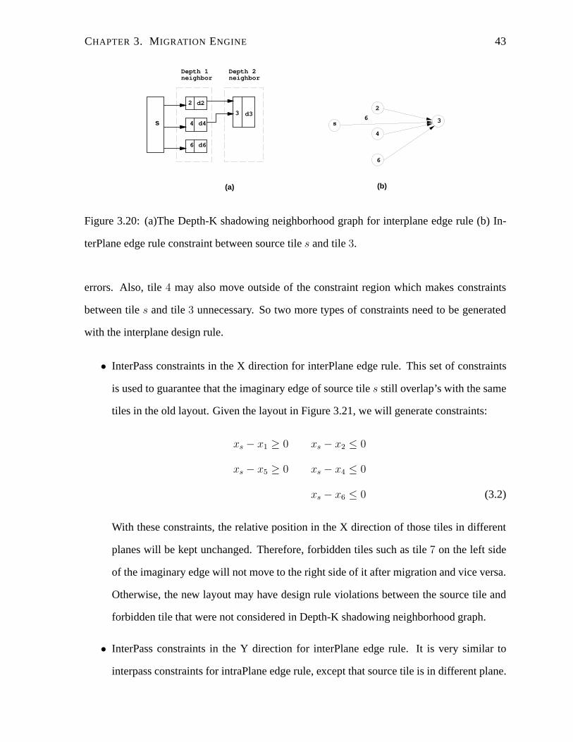
CHAPTER 3. MIGRATION ENGINE 43
2 d2
3 d3
(a) (b)
Depth 1neighbor
Depth 2neighbor
s 4 d4
6 d6
s
2
4
6
36
Figure 3.20: (a)The Depth-K shadowing neighborhood graph for interplane edge rule (b) In-
terPlane edge rule constraint between source tiles and tile3.
errors. Also, tile4 may also move outside of the constraint region which makes constraints
between tiles and tile3 unnecessary. So two more types of constraints need to be generated
with the interplane design rule.
• InterPass constraints in the X direction for interPlane edge rule. This set of constraints
is used to guarantee that the imaginary edge of source tiles still overlap’s with the same
tiles in the old layout. Given the layout in Figure 3.21, we will generate constraints:
xs − x1 ≥ 0 xs − x2 ≤ 0
xs − x5 ≥ 0 xs − x4 ≤ 0
xs − x6 ≤ 0 (3.2)
With these constraints, the relative position in the X direction of those tiles in different
planes will be kept unchanged. Therefore, forbidden tiles such as tile7 on the left side
of the imaginary edge will not move to the right side of it after migration and vice versa.
Otherwise, the new layout may have design rule violations between the source tile and
forbidden tile that were not considered in Depth-K shadowing neighborhood graph.
• InterPass constraints in the Y direction for interPlane edge rule. It is very similar to
interpass constraints for intraPlane edge rule, except that source tile is in different plane.

CHAPTER 3. MIGRATION ENGINE 44
For the layout in Figure 3.21, we need to generate constraints for the bottom edge of tile
s to guarantee that after migration, the bottom edge of tiles still overlaps with tiles that
overlapped with it in the original layout:
ys − y5 ≥ 0 ys − y1 ≤ 0
ys − y6 ≥ 0 ys − y4 ≤ 0
The constraints for top edge of tiles can be built in the same way. With this set of
constraints, the forbidden tiles in the checking plane will still stay within the constraint
region after migration. Other forbidden tiles that were above or below the constraint
region will be kept away from the constraint region so that no new violation will occur
after migration.
Figure 3.21 shows a real example of InterPlane constraints generated for leaf cell muxf201
given in Figure 3.15.
nwell:7
psubc:15
3
pdiff:152
6
pfet:146
6
pdiff:130
6
pdc:129
6
pdiff:128
6
pfet:125
6
pdiff:110
6
pdiff:108
6
pdiff:107
6
pfet:104
6
pdiff:88
6
pdc:87
6
pdiff:86
6
pfet:83
6
pdiff:67
6
pdiff:65
6
pdiff:64
6
pfet:60
6
pdiff:54
6
pdc:40
6
pdiff:38
6
pfet:35
6
pdiff:29
6
pdiff:20
6
ndc:150
1
ndiff:149
1
nfet:140
1
ndiff:137
1
ndc:135
1
ndiff:134
1
nfet:119
1
ndiff:116
1
ndc:115
1
ndiff:114
1
nfet:98
1
ndiff:95
1
ndc:93
1
ndiff:92
1
nfet:77
1
ndiff:73
1
ndc:72
1
ndiff:56
1
nfet:51
1
ndiff:48
1
ndc:45
1
psubc:158
1
psubc:25
1
space:156
0
poly:147
0
space:131
0
poly:126
0
space:111
0
poly:105
0
space:89
0
poly:84
0
space:68
0
poly:61
0
space:55
0
space:42
0
poly:36
0
space:30
0
space:22
0
space:16
0
space:17
0
space:18
0
space:19
0
pdc:21
0
pwell:8
0 6 6 6 6 6 6 6 66 6 6 6 6 6 6 3 3 3 3 0
6 66 66 666 66 6 6 666 6 6 6 6 6 6 3 3
space:159
0
poly:141
0
space:138
0
poly:120
0
space:117
0
poly:99
0
space:96
0
poly:78
0
space:74
0
space:57
0
poly:52
0
space:49
0
space:46
0
space:26
0
ndiff:47
0
space:9
6 6 6 6 6 6 6 6 6 6 6 60 3
space:13
0
0
0
space:160
0
0
0
Figure 3.21: InterPlane constraints generated for cell muxf201.
3.3.6 Connect Constraints Generation
Connect constraints are generated to guarantee the correct presentation of contact tiles after
migration. As we know from Chapter 2, corner-stitching partitions the mask layers into sepa-
rate planes. Layers that overlap may cause electrical constructs to be partitioned into the same
plane. Those layers that overlap with little electrical significance will be partitioned into differ-
ent planes [22]. For example, polysilicon, diffusion, and their overlaps (transistors) are stored
in active plane, while metal1 that does not interact with these layers is stored in a different
plane,metal1plane.
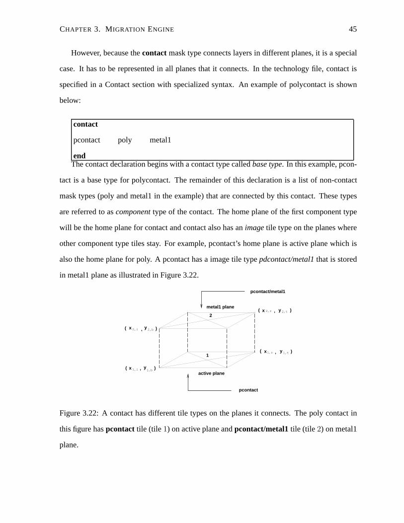
CHAPTER 3. MIGRATION ENGINE 45
However, because thecontact mask type connects layers in different planes, it is a special
case. It has to be represented in all planes that it connects. In the technology file, contact is
specified in a Contact section with specialized syntax. An example of polycontact is shown
below:
contact
pcontact poly metal1
endThe contact declaration begins with a contact type calledbase type. In this example, pcon-
tact is a base type for polycontact. The remainder of this declaration is a list of non-contact
mask types (poly and metal1 in the example) that are connected by this contact. These types
are referred to ascomponenttype of the contact. The home plane of the first component type
will be the home plane for contact and contact also has animagetile type on the planes where
other component type tiles stay. For example, pcontact’s home plane is active plane which is
also the home plane for poly. A pcontact has a image tile typepdcontact/metal1that is stored
in metal1 plane as illustrated in Figure 3.22.
pcontact/metal1
pcontact
metal1 plane
active plane
2
1
x y1,l 1,b,( )
x y2,l 2,b,( )
x y2,r 2,t,( )
x y1,r 1,t,( )
Figure 3.22: A contact has different tile types on the planes it connects. The poly contact in
this figure haspcontact tile (tile 1) on active plane andpcontact/metal1tile (tile 2) on metal1
plane.
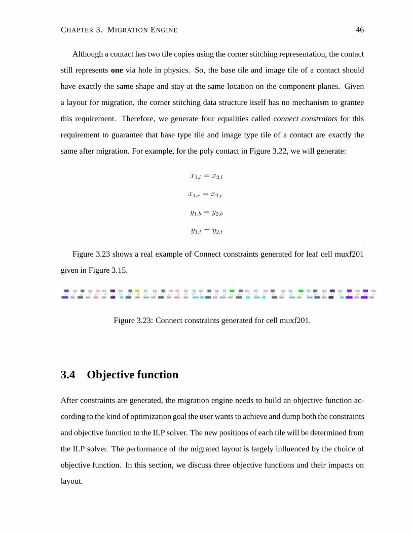
CHAPTER 3. MIGRATION ENGINE 46
Although a contact has two tile copies using the corner stitching representation, the contact
still representsone via hole in physics. So, the base tile and image tile of a contact should
have exactly the same shape and stay at the same location on the component planes. Given
a layout for migration, the corner stitching data structure itself has no mechanism to grantee
this requirement. Therefore, we generate four equalities calledconnect constraintsfor this
requirement to guarantee that base type tile and image type tile of a contact are exactly the
same after migration. For example, for the poly contact in Figure 3.22, we will generate:
x1,l = x2,l
x1,r = x2,r
y1,b = y2,b
y1,t = y2,t
Figure 3.23 shows a real example of Connect constraints generated for leaf cell muxf201
given in Figure 3.15.
psubc:15
psubc/m1:166
0 0
space:16
space:167
0 0
pdc:21
pdc/m1:173
0 0
space:22
space:174
0 0
pc:23
pc(m1):175
0 0
space:24
space:176
0 0
psubc:25
psubc:25
0 0
space:26
m1:178
0 0
pdc:40
pdc/m1:189
0 0
pdiff:41
space:190
0 0
ndc:45
ndc(m1):186
0 0
space:46
space:187
0 0
pdc:66
pdc/m1:198
0 0
space:68
space:199
0 0
pc:70
pc(m1):200
0 0
space:71
space:201
0 0
ndc:72
ndc(m1):202
0 0
space:74
m1:203
0 0
pdc:87
pdc/m1:212
0 0
space:89
space:213
0 0
ndc:93
ndc(m1):209
0 0
ndiff:94
space:210
0 0
pdc:109
pdc/m1:223
0 0
space:111
m1:224
0 0
ndc:115
ndc(m1):220
0 0
space:117
m1:221
0 0
pdc:129
pdc/m1:231
0 0
space:131
space:232
0 0
ndc:135
ndc(m1):240
0 0
ndiff:136
space:241
0 0
ndc:150
ndc(m1):248
0 0
pdc:155
pdc/m1:236
0 0
space:156
space:237
0 0
psubc:158
psubc:158
0 0
space:159
m1:251
0 0
via12:168
via12(m2):261
0 0
space:169
space:262
0 0
via12:246
via12(m2):289
0 0
space:247
space:290
0 0
Figure 3.23: Connect constraints generated for cell muxf201.
3.4 Objective function
After constraints are generated, the migration engine needs to build an objective function ac-
cording to the kind of optimization goal the user wants to achieve and dump both the constraints
and objective function to the ILP solver. The new positions of each tile will be determined from
the ILP solver. The performance of the migrated layout is largely influenced by the choice of
objective function. In this section, we discuss three objective functions and their impacts on
layout.
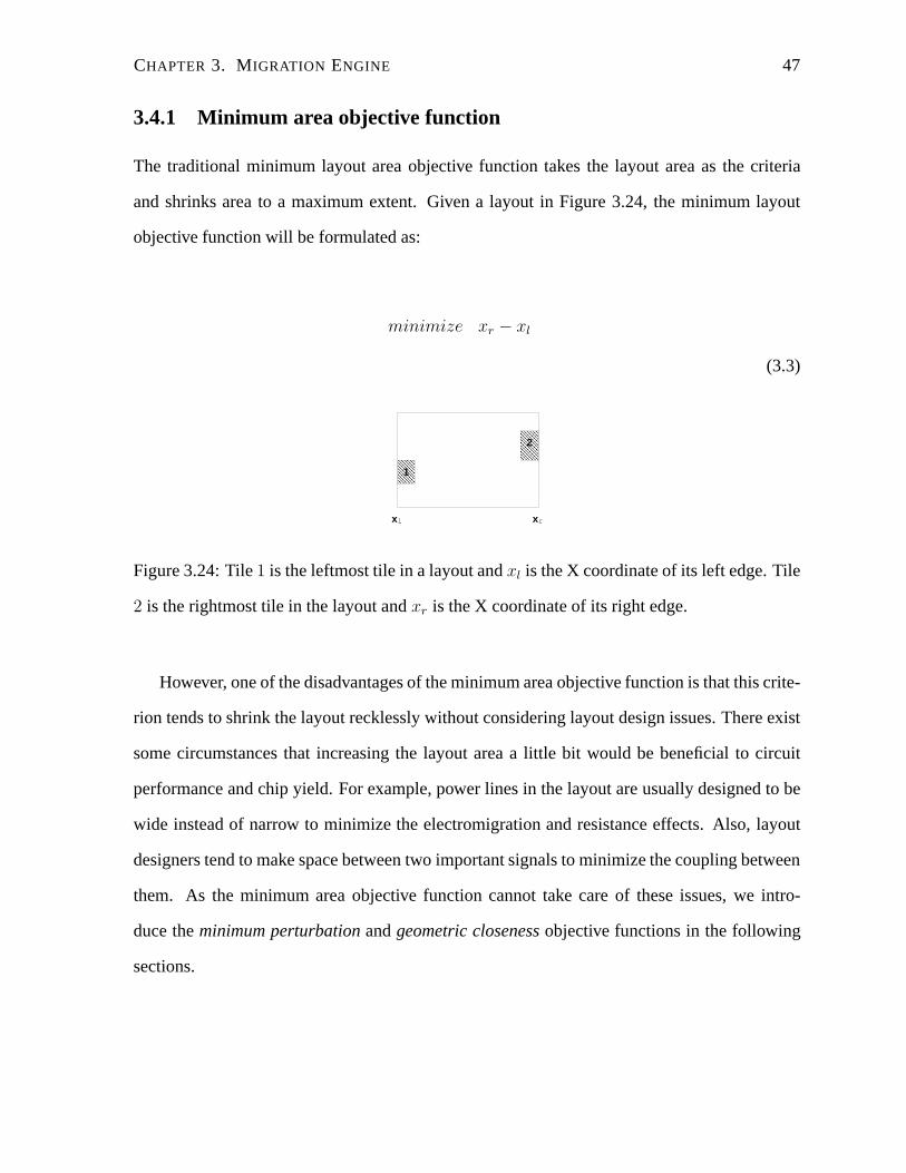
CHAPTER 3. MIGRATION ENGINE 47
3.4.1 Minimum area objective function
The traditional minimum layout area objective function takes the layout area as the criteria
and shrinks area to a maximum extent. Given a layout in Figure 3.24, the minimum layout
objective function will be formulated as:
minimize xr − xl
(3.3)
x l x r
1
2
Figure 3.24: Tile1 is the leftmost tile in a layout andxl is the X coordinate of its left edge. Tile
2 is the rightmost tile in the layout andxr is the X coordinate of its right edge.
However, one of the disadvantages of the minimum area objective function is that this crite-
rion tends to shrink the layout recklessly without considering layout design issues. There exist
some circumstances that increasing the layout area a little bit would be beneficial to circuit
performance and chip yield. For example, power lines in the layout are usually designed to be
wide instead of narrow to minimize the electromigration and resistance effects. Also, layout
designers tend to make space between two important signals to minimize the coupling between
them. As the minimum area objective function cannot take care of these issues, we intro-
duce theminimum perturbationandgeometric closenessobjective functions in the following
sections.

CHAPTER 3. MIGRATION ENGINE 48
3.4.2 Minimum perturbation objective function
In order to take full advantage of the original design and make minimum changes to the mi-
grated layout, theMinimum perturbationobjective is proposed in [10], which is defined as:
minimize∑
|x − xold| (3.4)
wherex is the vector of variables that determine X coordinates of all vertical edges andxold
is the vector of constants that are the original X coordinates of all vertical edges in the layout.
The minimum perturbation function minimizes the position changes of all edges and snaps
the edges to their original positions as much as possible. However, the disadvantage of this
function is that it minimizes the absolute coordinates of edges and will penalize more on the
movement of edges on the right side of the layout.
Example 6 Consider a simple layout given in Figure 3.25 with two tiles of metal2 type. Be-
cause of technology change, the minimum width requirement of tile 1 is changed from4λ to 5λ
and the distance requirement between tile 1 and tile 2 is changed from4λ to 5λ too. Based on
minimum perturbation objective function, the layout will be migrated to the one on the lower
part of Figure 3.25. The right edge of tile 1 will be stretched rightward by1λ and left edge of
tile 2 will be moved rightward by2λ. However, the right edge of tile 2 stays at the old posi-
tion because without change of its position, its width is5λ which satisfies the new design rule.
Otherwise, the objective function value will be greater than the one withx′2 unchanged.
It can been seen from this example that the movement of edges on the left side will add
penalties on the edges on the right side if we want to preserve the original shape of tiles on the
right.

CHAPTER 3. MIGRATION ENGINE 49
x0 4 5 8 10 15
before migration
after migration
tile 1 tile 2
x1 x1’ x2 x2’
Figure 3.25: The old layout and migrated layout with minimum perturbation objective function.
3.4.3 Geometric closeness objective function
To remove this penalty, a new objective function,geometric closenessobjective function is
introduced which is defined as :
Minimize∑
|(xri − xli) − (xoldri − xold
li )| (3.5)
Here,xri andxli are the X coordinates of the right and left edges of each tile in the layout.
The constantsxoldri andxold
li are the X coordinates of the right and left edges of the corresponding
tile in the original layout. Instead of minimizing the absolute coordinate changes of edges, this
function minimizes the shape changes of all tiles so that each tile change will not add penalty
to other tiles.
To linearize, or to remove the absolute value computation in Equation (3.5), we use a
method similar to [10] by introducing two variablesRi andLi for each tile, such that Equa-
tion (3.6) are introduced as constraints,
Ri ≥ xri − xli
Ri ≥ xoldri − xold
li
Li ≤ xri − xli
Li ≤ xoldri − xold
li (3.6)
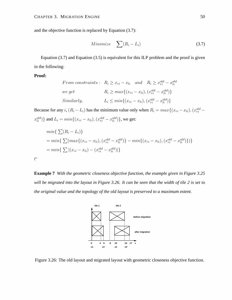
CHAPTER 3. MIGRATION ENGINE 50
and the objective function is replaced by Equation (3.7):
Minimize∑
(Ri − Li) (3.7)
Equation (3.7) and Equation (3.5) is equivalent for this ILP problem and the proof is given
in the following:
Proof:
From constraints : Ri ≥ xri − xli and Ri ≥ xoldri − xold
li
we get Ri ≥ max{(xri − xli), (xoldri − xold
li )}Similarly, Li ≤ min{(xri − xli), (x
oldri − xold
li )}Because for anyi, (Ri −Li) has the minimum value only whenRi = max{(xri −xli), (x
oldri −
xoldli )} andLi = min{(xri − xli), (x
oldri − xold
li )}, we get:
min{ ∑(Ri − Li)}
= min{ ∑(max{(xri − xli), (x
oldri − xold
li )} − min{(xri − xli), (xoldri − xold
li )})}= min{ ∑ |(xri − xli) − (xold
ri − xoldli )|}
2
Example 7 With the geometric closeness objective function, the example given in Figure 3.25
will be migrated into the layout in Figure 3.26. It can be seen that the width of tile 2 is set to
the original value and the topology of the old layout is preserved to a maximum extent.
x0 4 5 8 10 15
before migration
after migration
tile 1 tile 2
x1 x1’ x2 x2’
17
Figure 3.26: The old layout and migrated layout with geometric closeness objective function.

CHAPTER 3. MIGRATION ENGINE 51
3.5 Integer Linear Programming Solver
With all the constraints and the objective function generated, an integer linear programming
solver is needed to get the optimized solution for each variable. For all the test libraries, in-
cluding the datapath library and the standard cell library, there will be up to 2,000 variables
and 40,000 constraints (shown in Appendix A and B). We use the free ILP solver, called
lp solve, by Michel Berkelaar from Northwestern University and Argonne National Labora-
tory. (http://www.cs.sunysb.edu/ algorith/implement/lpsolve/implement.shtml). The program
can solve the ILP problem with as many as 30,000 variables and 50,000 constraints, which fits
our requirement. We can get a design rule clean layout after we assign the new position of each
tile from the result generated by ILP solver.

Chapter 4
Migration for datapath and standard cell
libraries
The migration engine described in Chapter 3 can migrate a layout to new technology without
design rule violations. However, it is not enough to handle migrating a library of leaf cells.
Today’s ASIC design flow prerequires the existence of library of cells that can be used for
synthesis or place & route tools. The total design is built from assembling these leaf cells in
the library. The design of leaf cells has more issues to consider so that they are compatible
with the synthesis or Place & Route tools. In this chapter, we will explore theoverall library
architecturerequirements for datapath and standard cell libraries and how these requirements
are solved using our migration engine.
4.1 Datapath library migration
In digital signal processing (DSP) ICs and microprocessors, the datapath is the core where all
computations are performed. A system’s performance is largely determined by the design and
implementation of its datapath. A datapath consists of interconnection of basic combinational
functions, such as logic ( AND, OR ) or arithmetic operators ( addition, multiplication, com-
52
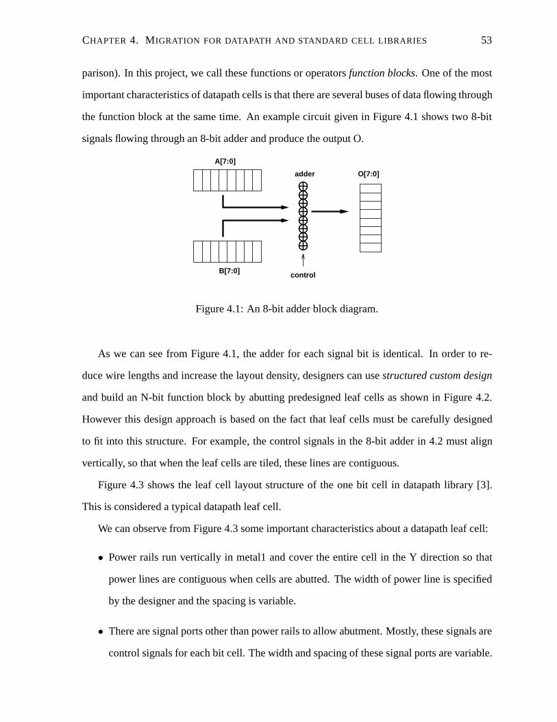
CHAPTER 4. MIGRATION FOR DATAPATH AND STANDARD CELL LIBRARIES 53
parison). In this project, we call these functions or operatorsfunction blocks. One of the most
important characteristics of datapath cells is that there are several buses of data flowing through
the function block at the same time. An example circuit given in Figure 4.1 shows two 8-bit
signals flowing through an 8-bit adder and produce the output O.
A[7:0]
B[7:0]
O[7:0]adder
control
Figure 4.1: An 8-bit adder block diagram.
As we can see from Figure 4.1, the adder for each signal bit is identical. In order to re-
duce wire lengths and increase the layout density, designers can usestructured custom design
and build an N-bit function block by abutting predesigned leaf cells as shown in Figure 4.2.
However this design approach is based on the fact that leaf cells must be carefully designed
to fit into this structure. For example, the control signals in the 8-bit adder in 4.2 must align
vertically, so that when the leaf cells are tiled, these lines are contiguous.
Figure 4.3 shows the leaf cell layout structure of the one bit cell in datapath library [3].
This is considered a typical datapath leaf cell.
We can observe from Figure 4.3 some important characteristics about a datapath leaf cell:
• Power rails run vertically in metal1 and cover the entire cell in the Y direction so that
power lines are contiguous when cells are abutted. The width of power line is specified
by the designer and the spacing is variable.
• There are signal ports other than power rails to allow abutment. Mostly, these signals are
control signals for each bit cell. The width and spacing of these signal ports are variable.
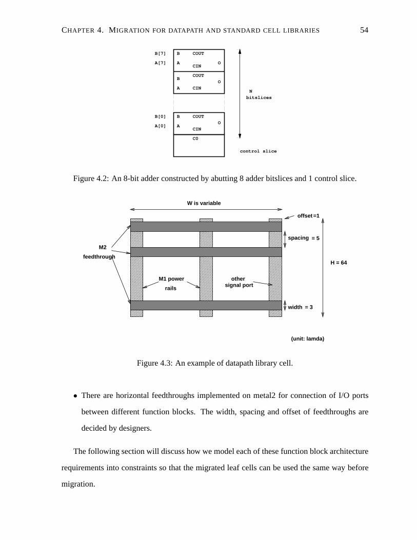
CHAPTER 4. MIGRATION FOR DATAPATH AND STANDARD CELL LIBRARIES 54
B
A O
COUT
CIN
B
A
COUT
CIN
O
B
A
COUT
CIN
O
C0
A[0]
B[0]
A[7]
B[7]
N
bitslices
control slice
Figure 4.2: An 8-bit adder constructed by abutting 8 adder bitslices and 1 control slice.
M2
feedthrough
M1 power
rails
other signal port
offset
spacing
width
W is variable
=1
(unit: lamda)
= 5
= 3
H = 64
Figure 4.3: An example of datapath library cell.
• There are horizontal feedthroughs implemented on metal2 for connection of I/O ports
between different function blocks. The width, spacing and offset of feedthroughs are
decided by designers.
The following section will discuss how we model each of these function block architecture
requirements into constraints so that the migrated leaf cells can be used the same way before
migration.
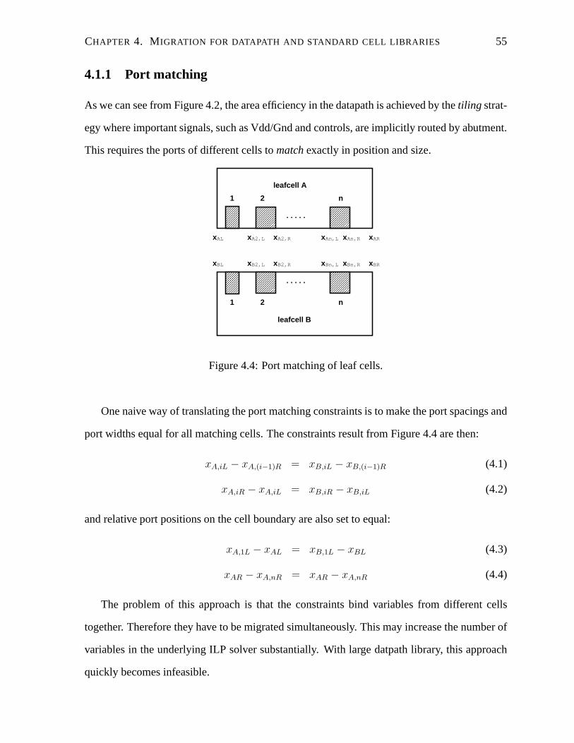
CHAPTER 4. MIGRATION FOR DATAPATH AND STANDARD CELL LIBRARIES 55
4.1.1 Port matching
As we can see from Figure 4.2, the area efficiency in the datapath is achieved by thetiling strat-
egy where important signals, such as Vdd/Gnd and controls, are implicitly routed by abutment.
This requires the ports of different cells tomatchexactly in position and size.
. . . . .
. . . . .
leafcell A
leafcell B
1 2
1 2
x
x x
x x x
x
x
x
ARAL
BL BR
A2,L A2,R
B2,L B2,R
An,L An,R
Bn,L Bn,R
x
xx
n
n
Figure 4.4: Port matching of leaf cells.
One naive way of translating the port matching constraints is to make the port spacings and
port widths equal for all matching cells. The constraints result from Figure 4.4 are then:
xA,iL − xA,(i−1)R = xB,iL − xB,(i−1)R (4.1)
xA,iR − xA,iL = xB,iR − xB,iL (4.2)
and relative port positions on the cell boundary are also set to equal:
xA,1L − xAL = xB,1L − xBL (4.3)
xAR − xA,nR = xAR − xA,nR (4.4)
The problem of this approach is that the constraints bind variables from different cells
together. Therefore they have to be migrated simultaneously. This may increase the number of
variables in the underlying ILP solver substantially. With large datpath library, this approach
quickly becomes infeasible.

CHAPTER 4. MIGRATION FOR DATAPATH AND STANDARD CELL LIBRARIES 56
We instead introduce a pair of constants,d andw to break the dependency between different
cells:
xA,iL − xA,(i−1)R = d xB,iL − xB,(i−1)R = d (4.5)
xA,iR − xA,iL = w xB,iR − xB,iL = w (4.6)
Becaused and w are constants, with constraints in Equation 4.5 and 4.6 leaf cells can
still be migrated separately. However, the value ofd andw must be carefully selected so that
constraints in Equation 4.5 and 4.6 do not conflict with design rule constraints described in
Chapter 3. To address this problem, we employ a dual-pass strategy that is elaborated below:
• In the first pass, it analyzes the layout of each leaf cell, generates the design rule con-
straints, and drives an ILP solver under the objective function that the designer needs to
arrive at a temporary migration solution of each cell as shown in Figure 4.5. Note that
the ILP problems are solved separately for different cells.
• In the second pass, the different architectural and circuit requirements are translated
into linear constraints, such as the port matching constraints in Equation 4.5. Here, the
temporary solution obtained in the first pass is exploited so that the new constraints relate
variables originating from the same cell. The ILP solver is then called again to obtain
the new and final solution to accommodate the new constraints. Note again that the ILP
problems are solved separately for each cell.
Using this dual-pass strategy, We obtaind andw by taking the maximum value ofx′iL −
x′(i−1)R, andx
′iR−x
′iL among all the leaf cells that have to be matched, wherex
′is the temporary
solution we obtain in the first pass. This method effectively stretches the port whose width or
spacing to the previous port can be smaller than the maximum value among all the leaf cells,
making all ports align together without design rule violations.
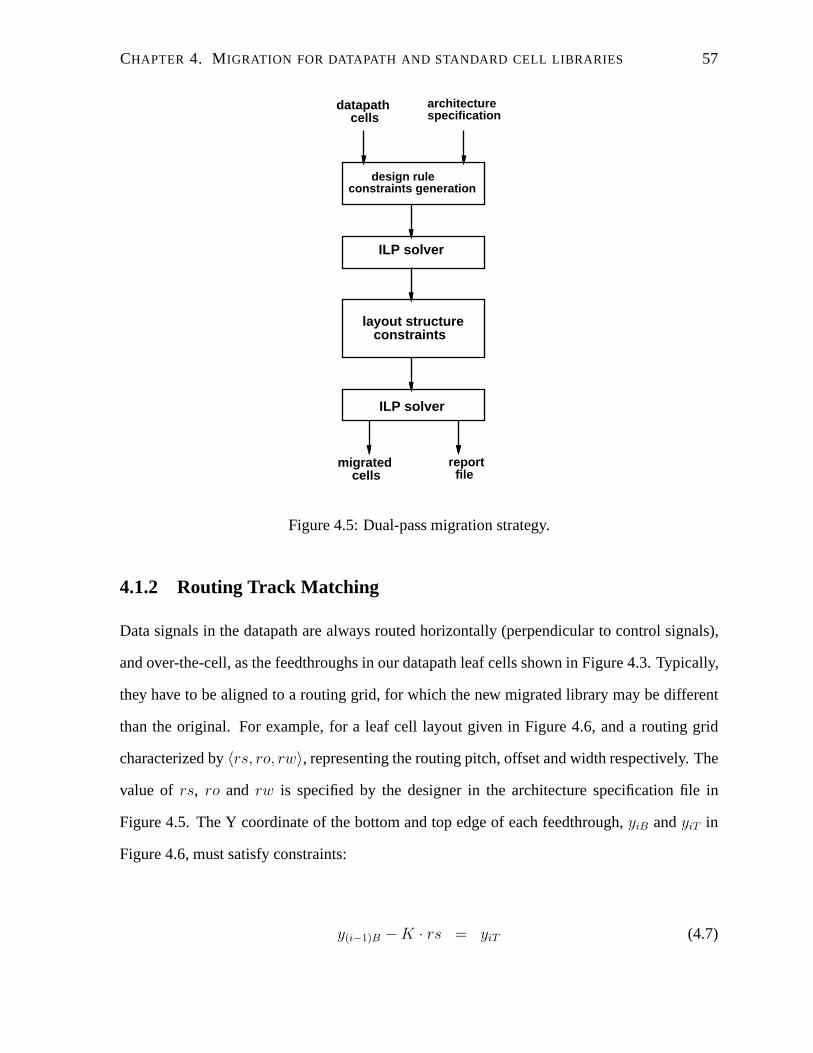
CHAPTER 4. MIGRATION FOR DATAPATH AND STANDARD CELL LIBRARIES 57
design ruleconstraints generation
ILP solver
layout structure constraints
ILP solver
report file
architecture specification
datapath cells
migrated cells
Figure 4.5: Dual-pass migration strategy.
4.1.2 Routing Track Matching
Data signals in the datapath are always routed horizontally (perpendicular to control signals),
and over-the-cell, as the feedthroughs in our datapath leaf cells shown in Figure 4.3. Typically,
they have to be aligned to a routing grid, for which the new migrated library may be different
than the original. For example, for a leaf cell layout given in Figure 4.6, and a routing grid
characterized by〈rs, ro, rw〉, representing the routing pitch, offset and width respectively. The
value of rs, ro and rw is specified by the designer in the architecture specification file in
Figure 4.5. The Y coordinate of the bottom and top edge of each feedthrough,yiB andyiT in
Figure 4.6, must satisfy constraints:
y(i−1)B − K · rs = yiT (4.7)
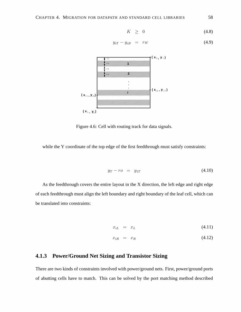
CHAPTER 4. MIGRATION FOR DATAPATH AND STANDARD CELL LIBRARIES 58
K ≥ 0 (4.8)
yiT − yiB = rw (4.9)
.
.
.
( )x yL
R
B
T
,
x( y ),
( x iL iB
iTiR
, y )
( x , y )
ro
rw
rs
rw 1
2
i
Figure 4.6: Cell with routing track for data signals.
while the Y coordinate of the top edge of the first feedthrough must satisfy constraints:
yT − ro = y1T (4.10)
As the feedthrough covers the entire layout in the X direction, the left edge and right edge
of each feedthrough must align the left boundary and right boundary of the leaf cell, which can
be translated into constraints:
xiL = xL (4.11)
xiR = xR (4.12)
4.1.3 Power/Ground Net Sizing and Transistor Sizing
There are two kinds of constraints involved with power/ground nets. First, power/ground ports
of abutting cells have to match. This can be solved by the port matching method described
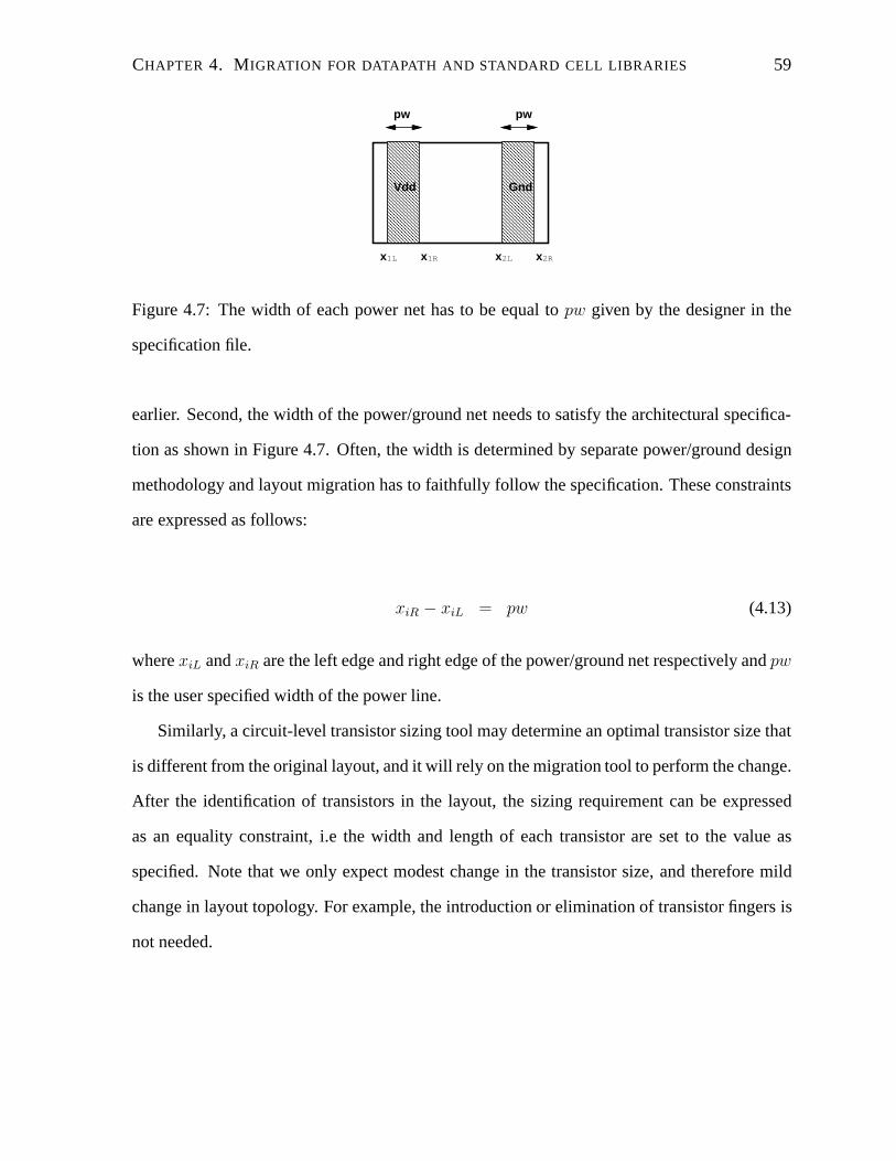
CHAPTER 4. MIGRATION FOR DATAPATH AND STANDARD CELL LIBRARIES 59
Vdd Gnd
x x x x1L 1R 2L 2R
pw pw
Figure 4.7: The width of each power net has to be equal topw given by the designer in the
specification file.
earlier. Second, the width of the power/ground net needs to satisfy the architectural specifica-
tion as shown in Figure 4.7. Often, the width is determined by separate power/ground design
methodology and layout migration has to faithfully follow the specification. These constraints
are expressed as follows:
xiR − xiL = pw (4.13)
wherexiL andxiR are the left edge and right edge of the power/ground net respectively andpw
is the user specified width of the power line.
Similarly, a circuit-level transistor sizing tool may determine an optimal transistor size that
is different from the original layout, and it will rely on the migration tool to perform the change.
After the identification of transistors in the layout, the sizing requirement can be expressed
as an equality constraint, i.e the width and length of each transistor are set to the value as
specified. Note that we only expect modest change in the transistor size, and therefore mild
change in layout topology. For example, the introduction or elimination of transistor fingers is
not needed.
CHAPTER 4. MIGRATION FOR DATAPATH AND STANDARD CELL LIBRARIES 60
4.1.4 Soft Constraints
A practical problem frequently encountered is that it is highly possible that the layout archi-
tecture specified by the user may lead to infeasible solutions. For example, if the routing pitch
rs and routing widthrw are too small, the routing grid constraints may conflict with minimum
spacing requirement and minimum width requirement on metal2 specified by design rules in
the new technology file. The ILP solver only provides a binary answer of failure when the
given constraints are conflicting with each other. To make things worse, a typical leaf cell may
have over thousands of constraints. it is unlikely that the user can trace where the conflicting
constraints are and make a decision on where to change architecture specification or manually
modify the layout at some specific location. It is instead highly desirable for the tool to provide
some hints.
We introduce a new concept, calledsoft constraintsto address this problem. Typically, the
constraints that are related to architecture specification given by the designer, such as routing
track constraints, power/ground sizing constraints, and transistor sizing constraints, will be in-
troduced as soft constraints, in contrast to hard constraints such as design rule constraints. One
of the characteristics of these constraints is that they are all expressed as equalities. Consider
such equality constraints expressed in the form of:
∑
j
Aijxj = bi (4.14)
WhereAij is the coefficient matrix, andbi is a vector of constraints. We introduce two
positive variables, calledelastic variablesei1 andei2 that will be added to the equality:
∑
j
Aijxj + ei1 − ei2 ≥ bi (4.15)
ei1 ≥ 0 (4.16)
ei2 ≥ 0 (4.17)
CHAPTER 4. MIGRATION FOR DATAPATH AND STANDARD CELL LIBRARIES 61
Since the values ofei1 − ei2 can be set arbitrarily in value, the original constraint can be
relaxed orsoftened, in other words, the equalities do not have to be satisfied. This effectively
enlarges the feasible solution space of the ILP problem.
On the other hand, it is highly possible that the soft variables may make those constraints
that can be satisfied become infeasible by setting the soft variables to a non-zero value. To
prevent unnecessary constraints relaxation, we penalize those solutions that were not supposed
to be feasible originally by adding them to the objective function with a large weighting factor.
Combining Equation (3.5), the new objective function becomes
∑
j
(Rj − Lj) + W∑
i
(ei1 + ei2) (4.18)
This way, if conflicting constraints exist, by looking for all non-zero elastic variables, users
can easily pinpoint the wrong specifications and revise them accordingly.
4.2 Standard Cell Library Migration
Standard cell library is the basic library used for most ASIC designs. It provides functional
blocks such as inverters, NANDs, and flip-flops used for synthesis and layout presentation of
these function blocks for place & route. An example of design implemented with standard cell
library that consists of rows of standard cells and channels between them is given in Figure 4.8
[14]. More advanced design with more than two layers for routing may not leave the space for
channels which means that routings are all done over the cell.
There are several factors that impact the design of standard cell libraries. First, with the
modern synthesis design flow, circuit designers usually do not see the layout cells. So there
is great need for standardization of leaf cells in the library. The standardization includes the
requirements such as [7]:
• The shape of leaf cells must be rectangle.
• Cells in the same row or in particular are all of the same height.
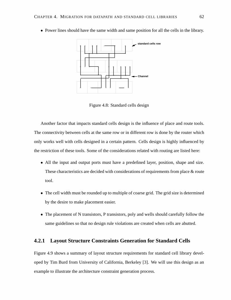
CHAPTER 4. MIGRATION FOR DATAPATH AND STANDARD CELL LIBRARIES 62
• Power lines should have the same width and same position for all the cells in the library.
standard cells row
Channel
Figure 4.8: Standard cells design
Another factor that impacts standard cells design is the influence of place and route tools.
The connectivity between cells at the same row or in different row is done by the router which
only works well with cells designed in a certain pattern. Cells design is highly influenced by
the restriction of these tools. Some of the considerations related with routing are listed here:
• All the input and output ports must have a predefined layer, position, shape and size.
These characteristics are decided with considerations of requirements from place & route
tool.
• The cell width must be rounded up to multiple of coarse grid. The grid size is determined
by the desire to make placement easier.
• The placement of N transistors, P transistors, poly and wells should carefully follow the
same guidelines so that no design rule violations are created when cells are abutted.
4.2.1 Layout Structure Constraints Generation for Standard Cells
Figure 4.9 shows a summary of layout structure requirements for standard cell library devel-
oped by Tim Burd from University of California, Berkeley [3]. We will use this design as an
example to illustrate the architecture constraint generation process.
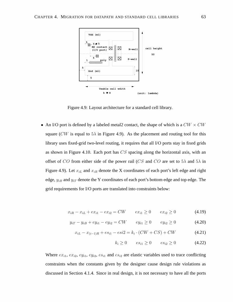
CHAPTER 4. MIGRATION FOR DATAPATH AND STANDARD CELL LIBRARIES 63
Vdd (m1)
Gnd (m1)
N−well
P−well
55 5
M2 contact(I/O port)
5
5
10
cell height
Usable cell wdith
k 8 (unit: lambda)
poly5
50
1
Figure 4.9: Layout architecture for a standard cell library.
• An I/O port is defined by a labeled metal2 contact, the shape of which is aCW × CW
square (CW is equal to5λ in Figure 4.9). As the placement and routing tool for this
library uses fixed-grid two-level routing, it requires that all I/O ports stay in fixed grids
as shown in Figure 4.10. Each port hasCS spacing along the horizontal axis, with an
offset of CO from either side of the power rail (CS andCO are set to5λ and5λ in
Figure 4.9). LetxiL andxiR denote the X coordinates of each port’s left edge and right
edge,yiB andyiT denote the Y coordinates of each port’s bottom edge and top edge. The
grid requirements for I/O ports are translated into constraints below:
xiR − xiL + exi1 − exi2 = CW exi1 ≥ 0 exi2 ≥ 0 (4.19)
yiT − yiB + eyi1 − eyi2 = CW eyi1 ≥ 0 eyi2 ≥ 0 (4.20)
xiL − x(i−1)R + esi1 − esi2 = ki · (CW + CS) + CW (4.21)
ki ≥ 0 esi1 ≥ 0 esi2 ≥ 0 (4.22)
Whereexi1, exi2, eyi1, eyi2, esi1 andesi2 are elastic variables used to trace conflicting
constraints when the constants given by the designer cause design rule violations as
discussed in Section 4.1.4. Since in real design, it is not necessary to have all the ports
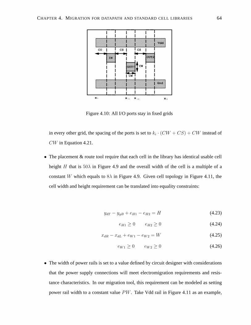
CHAPTER 4. MIGRATION FOR DATAPATH AND STANDARD CELL LIBRARIES 64
CS CSCO
CW
CW
x x x xL RiL iR
Vdd
Gnd
IN
OUT!
OUT2
Figure 4.10: All I/O ports stay in fixed grids
in every other grid, the spacing of the ports is set toki · (CW + CS) + CW instead of
CW in Equation 4.21.
• The placement & route tool require that each cell in the library has identical usable cell
heightH that is50λ in Figure 4.9 and the overall width of the cell is a multiple of a
constantW which equals to8λ in Figure 4.9. Given cell topology in Figure 4.11, the
cell width and height requirement can be translated into equality constraints:
ydT − ygB + eH1 − eH2 = H (4.23)
eH1 ≥ 0 eH2 ≥ 0 (4.24)
xdR − xdL + eW1 − eW2 = W (4.25)
eW1 ≥ 0 eW2 ≥ 0 (4.26)
• The width of power rails is set to a value defined by circuit designer with considerations
that the power supply connections will meet electromigration requirements and resis-
tance characteristics. In our migration tool, this requirement can be modeled as setting
power rail width to a constant valuePW . Take Vdd rail in Figure 4.11 as an example,
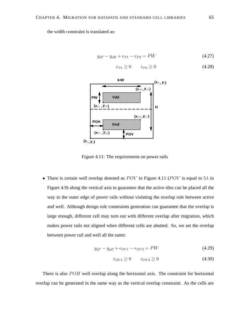
CHAPTER 4. MIGRATION FOR DATAPATH AND STANDARD CELL LIBRARIES 65
the width constraint is translated as:
ydT − ydB + eP1 − eP2 = PW (4.27)
eP1 ≥ 0 eP2 ≥ 0 (4.28)
(x y )L,
(x y )R T,
(x
dL dB
B
y, )
(x y, )
dR dT
(x y, )
(x y, )
gL gB
gR gT
Vdd
GndPOH
POV
PW
k W
H
Figure 4.11: The requirements on power rails
• There is certain well overlap denoted asPOV in Figure 4.11 (POV is equal to5λ in
Figure 4.9) along the vertical axis to guarantee that the active tiles can be placed all the
way to the outer edge of power rails without violating the overlap rule between active
and well. Although design rule constraints generation can guarantee that the overlap is
large enough, different cell may turn out with different overlap after migration, which
makes power rails not aligned when different cells are abutted. So, we set the overlap
between power rail and well all the same:
ygT − ygB + eOV 1 − eOV 2 = PW (4.29)
eOV 1 ≥ 0 eOV 2 ≥ 0 (4.30)
There is alsoPOH well overlap along the horizontal axis. The constraint for horizontal
overlap can be generated in the same way as the vertical overlap constraint. As the cells are

CHAPTER 4. MIGRATION FOR DATAPATH AND STANDARD CELL LIBRARIES 66
abutted along horizontal axis, all active, metal1 and metal2 tiles must be contained within two
power rails. This is guaranteed by the original careful design because migration will not make
drastic topology changes which means that the tiles inside power rails will not move outside
after migration.
Chapter 5
Experiments and Conclusion
5.1 Experimental Setup
We implemented the migration tool on top of an IP-centric CAD infrastructure, calledipsuite,
which uses Magic’s corner stitching data structure to represent mask layout. An open-source
ILP solverlp solve, by Michel Berkelaar from Northwestern University and Argonne National
Laboratory, is used to generate the optimized result. For all the test libraries, including the
datapath library and the standard cell library, there will be up to 2,000 variables and 40,000
constraints (shown in Appendix A and B). The ILP solver can solve the ILP problem with as
many as 30,000 variables and 50,000 constraints, which fits our requirement. The migration
tool itself is implemented by over 12,000 lines of C code.
To test the effectiveness of our tool, we apply our tool on the low-power standard library
and datapath library developed by Burd [3] at University of California, Berkeley. Standard
cell library contains 94 leaf cells that include the range of 2, 3 and 4 input “simple” gates –
nand/and, nor/or, muxes, and-or/or-and, etc. There are various-sized inverters, buffers, trans-
mission gates and a small variety of simple latches. Different types of adder and subtracter bit
slices are also included in the standard cell library. The datapath library contains 285 cells that
have a wide variety of functions as those in standard cell library. Several chips such as protocol
67
CHAPTER 5. EXPERIMENTS AND CONCLUSION 68
chip, video decompression chip set are designed with these libraries [3]. Both standard cell
library and datapath library are implemented based on standard MOSIS1.2µm process. Our
targeted process is TSMC 0.25µm and TSMC 0.18µm technologies.
In the following sections, we show the experimental results to demonstrate each feature of
our migration tool. Section 5.2.1 gives the run time result for constraint generation algorithm
and ILP solver. The run time for constraint generation is found to be propotional toO(N1.4). In
order to demonstrate thatDual-pass strategyis effective in solving hierachical layout migration
problems, such as pitch matching problem, we give the experimental results of migrating leaf-
cells for aN bit adder in datapath library, and migrating two datapath library cellsandf201 and
muxf201 with respect to layout architecture requirements in section 5.2.2. Thesoft constraints
method is tested in section 5.2.4 with an example migration result of a standard cell. And the
soft constraint method is found to be effective in correcting wrong constraints and guiding
the users to fix them. Finally, a comparision of different objective functions is presented in
section 5.2.3 with migration result of a standard cell under different objective functions.
5.2 Experimental Result
5.2.1 Run Time
The run time of datapath library and standard cell library is summarized in Appendix . Fig-
ure 5.1 gives a plot of run time versus number of tiles in the layout. The solid line in the figure
shows the run time (measured in seconds) of constraints generation for standard cells versus
the number of tilesN . And the dotted line is the plot of function proportional tof(N) = N1.4.
The run time in Figure 5.1 includesIntraPlane, InterPlane, InterPassandConnectcon-
straint generation. Except fromConnectconstraint generation, other constraint generation
algorithms are all based onDepth-K searchingalgorithm. Because most layouts have very few
contacts, we can assume that this rum time is dominated by the run time of constraint gen-
eration usingDepth-K searchingalgorithm. As can been seen from Figure 5.1, this real run
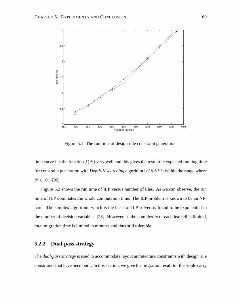
CHAPTER 5. EXPERIMENTS AND CONCLUSION 69
150 200 250 300 350 400 450 500 550 600 6500
0.5
1
1.5
2
2.5
3
N:number of tiles
run
time
(s)
Figure 5.1: The run time of design rule constraint generation
time curve fits the functionf(N) very well and this gives the result:the expected running time
for constraint generation withDepth-K searchingalgorithm isO(N1.4) within the range where
N ∈ [0 : 700].
Figure 5.2 shows the run time of ILP versus number of tiles. As we can observe, the run
time of ILP dominates the whole computation time. The ILP problem is known to be an NP-
hard. The simplex algorithm, which is the basis of ILP solver, is found to be exponential in
the number of decision variables [23]. However, as the complexity of each leafcell is limited,
total migration time is limited in minutes and thus still tolerable.
5.2.2 Dual-pass strategy
Thedual-pass strategyis used to accommodate layout architecture constraints with design rule
constraints that have been built. In this section, we give the migration result for the ripple carry

CHAPTER 5. EXPERIMENTS AND CONCLUSION 70
150 200 250 300 350 400 450 500 550 600 6500
50
100
150
200
250
Figure 5.2: The run time of ILP solver.
adder in datapath library and two leafcells in standard cell library to demonstrate the result for
this algorithm.
In this datapath library, there are four leafcells used for building a ripple carry adder. Cell
add and celladd fast are full adder bit slices. Celladd cs sel and add cs 0 are control
slices used to determine the carry-in signal for the least significant bit adder cell. Figure 5.3
shows the leafcells before migration and after migration. The old layouts are based on standard
MOSIS1.2µm technology, and the news cells are generated after the migration process under
the geometric closeness objective function. The targeted process is TSMC 0.25µm technology.
Note that the layouts are displayed with measurement unit set to2λ.
The usage of these cells for building an N bit adder are visualized in Figure 5.4.
The layout architecture characteristics before migration and after migration are summarized
in Table 5.1.
Figure 5.5(a) and (b) shows a four-bit adder built from old leafcells and from migrated
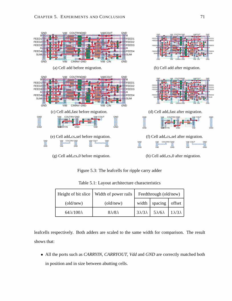
CHAPTER 5. EXPERIMENTS AND CONCLUSION 71
���������������������������������������������������������������������������������
������������������������������������������������������������������������
������������������������������������
���������������������������������������������������������������
���������������������������������������������
����
����
����
���������� ������� ��
����
����
����
������������
������
�������� ��
�����
�����
�������� ��
��
����
�����
�������
���� ��
��
����
��
�� �
������������������� ��
��
��
��
��
��
������
������
��������
������������
���� ����
���������������
� �
���� �������������� ��
��������������
� ���
�����������
����
������������
�� ��
�������
����������
� �������
�����
������ �����
��� ����
��
��
��
������� ���
�� ������
��������
�� ���� ��
� ����
����
��
���� �� ��
���������
����
����
���
����������� �������
������� ��
����
������
��
������������
���������
����
��
�����������
���
���
�������
������� ��
�� ����
����������������
���
��� � ��
����
������� ������
� ���������� �
������� �������
����
�� ���
������������
����������
����������
������
������
�����
��������
���
�� � ����
����
����
���� ������� ��
��� ����� ��
��
� �������
�����
������ �����
��� ����
��
��
��
������� ���
�� ������
��������
�� ���� ��
� ����
����
��
���� �� ��
���������
���
����
����
������������������
���
����
����
����
���� ��
��
����
Vdd VddCOUT
CIN
GNDCOUTINV
CININVGND GNDVddVdd
GNDB
FEED1FEED2FEED3
AFEED4
SUM
BFEED1FEED2FEED3AFEED4SUM
GND
GND
������������������������������������������������
������������������������������������������������
������������������������
��������������������������������
������������������������
����
���������������������
���
���������� ������� ��
������
�������������� ��
��
����
����� ��
������
���� ��
����
������
�������������� �
����
��
����
������
��
�������� ���
�������� �
�� ������� �
�������
�� ������� �
������������������������������
�� �� ���
������
����
��� �
����
���� ��
����
��
��������
� ������
���
��
����
�� ��
��������
��
����
� �� ��
���������
�������
��������������
����� �������
����
������������������
����������
���������
�����
��������
���
� �����
��������������
����� ��
����������
�������������� ��
����������� ��
���������������
��������������
��������
�������������������
�
��
�������� �
������
�
�� �� ���
������
����
��� �
����
���� ��
����
��
��������
� ������
���
��
����
�� ��
��������
��
����
� �� ����������
����
��
��
��������
��
���� �
�
��
�� ��
��
��
GND Vdd CININV GND Vdd CIN GND
GND Vdd COUTINV GND VddCOUT GND
SUMFEED4
AFEED3
FEED2FEED1B
SUMFEED4
AFEED3
FEED2FEED1
B
(a) Cell add before migration. (b) Cell add after migration.
���������������������������������������������������������������������������������
������������������������������������������������������������������������
������������������������������������
���������������������������������������������������������������
���������������������������������������������
����
����
����
���������� ������� ��
����
����
���������
������������
������
�������� ��
�����
�����
�������� ��
��
����
����������
�������
���� ��
��
����
��
�� �
������������������� �����
��
��
��
��
����
������
������
�����������
������������
���� ����
���������������
�� ��
���� �������������� ��
��������������
���� �����������
�����������
����
������������
�� ��
�������
����������
� �������
�����
������ �����
��� ����
����
����
����
������� ���
�� ������
��������
�� ���� ��
� ����
����
��
���� �� ��
���������
����
����
���
����������� �������
������� ��
����
������
��
������������
���������
����
��
������������
���
�����������
������� ��
�� ����
����������������
���
��� � ��
����
������� ������
� ���������� �
������� �������
����
�� ���
������������
����
����
����������
������
������
�����
����
��
���
�� � ����
����
����
���� ������� ��
��� ����� ��
��
� �������
�����
������ �����
��� ����
����
����
����
������� ���
�� ������
��������
�� ���� ��
� ����
����
��
���� �� ��
���������
���
����
����
������������������
���
����
����
����
���� ��
��
����
GND Vdd VddCOUT
CIN
GNDCOUTINV
CININVGND GNDVddVdd
BFEED1FEED2FEED3
AFEED4
SUM
BFEED1FEED2FEED3AFEED4SUM
GND
GND
������������������������������������������������
������������������������������������������������
������������������������
��������������������������������
������������������������
����
�����������������
�������
������������
����
������� ��
������
���������������� ��
��
����
��������� ��
������
���� ��
��
����
������
������������ ���
����
��
�������
������
�����
���
�������� ��
����������
�� ��
�� ������� �
�������
���� �������������� �
����������������� �
�������
�� �� �����
����
������
��� �
������ ��
����
����
������ �
� ��������
��
���
���� ���� ��
������
��
����
� �� ��
���������
�������
��������������
����� ���������
����
��������
����������������
����������
�������
���
������
����� � ��
����
��������������
����� ��
��������������������� ��
����������� ��
�� ��������������
������������
��������
������������
���� ����
��
��������
� �������� �
�� �� �����
����
������
��� �
������ ��
����
����
������ �
� ��������
��
���
���� ���� ��
������
��
����
� �� ����������
����
��
��
��������
��
���� �
�
����
�� ��
��
��
GND Vdd CININVGND Vdd CIN GND
GND Vdd COUTINVGND VddCOUT GND
SUMFEED4
AFEED3FEED2FEED1
B
SUMFEED4
AFEED3FEED2FEED1
B
(c) Cell addfast before migration. (d) Cell addfast after migration.
���������������
���������������
�������������������������
���� �
�
����
��
���� �
������������� ���� ������
���
������������
��������
�� ���� ����
���
��
GND GND GNDVddVdd COUTINV COUT
GNDCARRYINVdd Vdd GNDGND ������������
������������
��������������������
�� �
�
����
��
���� �
������������� ��� ��������������
�������� �
�
������ ��� �
������
���
������
GND VddCARRYIN GND Vdd GND
GND Vdd COUTINV GND Vdd COUT GND
(e) Cell addcs sel before migration. (f) Cell addcs sel after migration.
GND Vdd Vdd COUT GNDGNDCOUTINV
GND Vdd GND GNDVdd
GND Vdd GND Vdd GND
GND Vdd COUTINV GND Vdd COUT GND
(g) Cell addcs 0 before migration. (h) Cell addcs 0 after migration.
Figure 5.3: The leafcells for ripple carry adder
Table 5.1: Layout architecture characteristics
Height of bit slice Width of power rails Feedthrough (old/new)
(old/new) (old/new) width spacing offset
64λ/100λ 8λ/8λ 3λ/3λ 5λ/6λ 1λ/3λ
leafcells respectively. Both adders are scaled to the same width for comparison. The result
shows that:
• All the ports such asCARRYIN, CARRYOUT, VddandGND are correctly matched both
in position and in size between abutting cells.
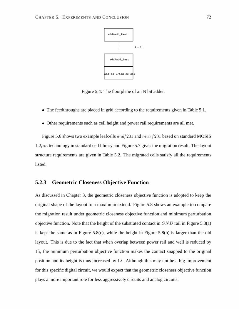
CHAPTER 5. EXPERIMENTS AND CONCLUSION 72
.
.
.
add_cs_0/add_cs_sel
add/add_fast
add/add_fast
[1..N]
Figure 5.4: The floorplane of an N bit adder.
• The feedthroughs are placed in grid according to the requirements given in Table 5.1.
• Other requirements such as cell height and power rail requirements are all met.
Figure 5.6 shows two example leafcellsandf201 andmuxf201 based on standard MOSIS
1.2µm technology in standard cell library and Figure 5.7 gives the migration result. The layout
structure requirements are given in Table 5.2. The migrated cells satisfy all the requirements
listed.
5.2.3 Geometric Closeness Objective Function
As discussed in Chapter 3, the geometric closeness objective function is adopted to keep the
original shape of the layout to a maximum extend. Figure 5.8 shows an example to compare
the migration result under geometric closeness objective function and minimum perturbation
objective function. Note that the height of the substrated contact inGND rail in Figure 5.8(a)
is kept the same as in Figure 5.8(c), while the height in Figure 5.8(b) is larger than the old
layout. This is due to the fact that when overlap between power rail and well is reduced by
1λ, the minimum perturbation objective function makes the contact snapped to the original
position and its height is thus increased by1λ. Although this may not be a big improvement
for this specific digital circuit, we would expect that the geometric closeness objective function
plays a more important role for less aggressively circuits and analog circuits.
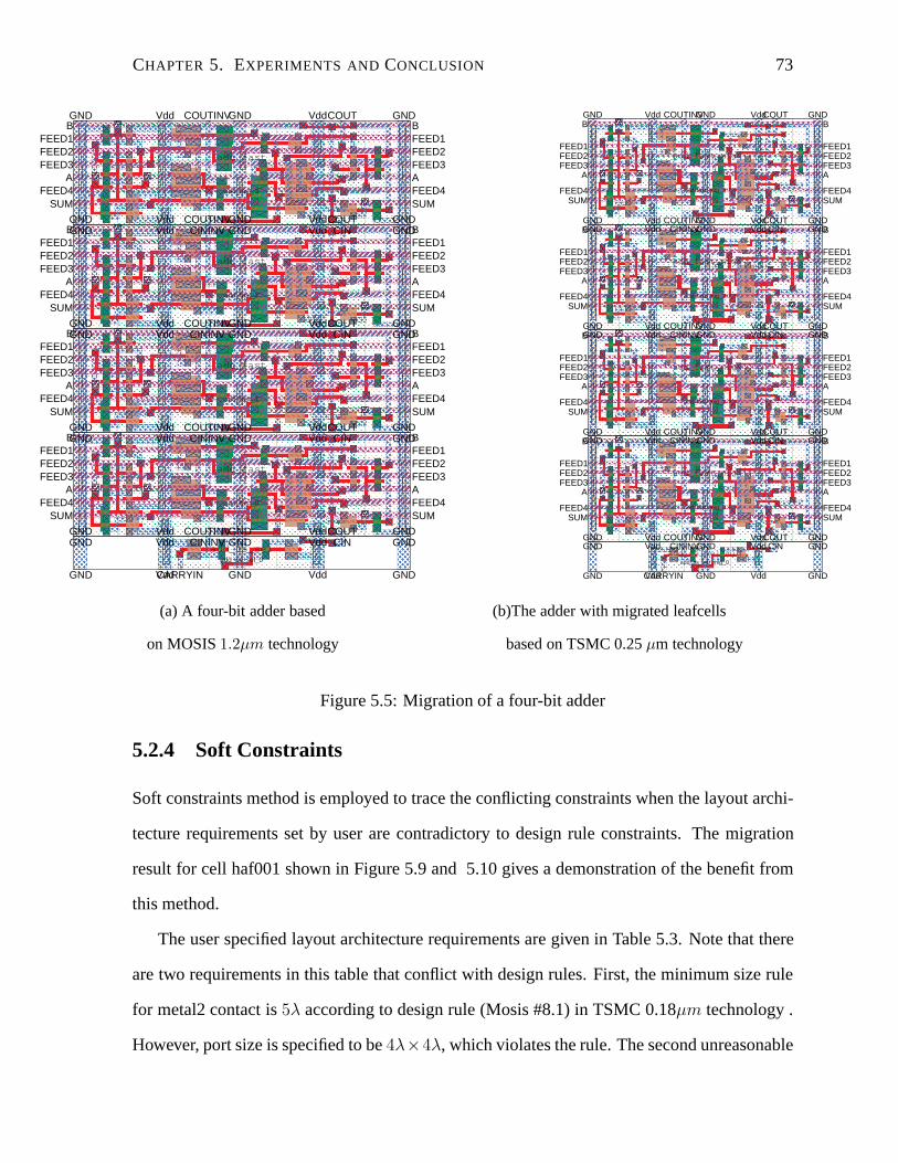
CHAPTER 5. EXPERIMENTS AND CONCLUSION 73
������������������������������������������������������������������������������������������
��������������������������������������������������������������������������������
������������������������������������������������������������������������������������������
��������������������������������������������������������������������������������
������������������������������������������������������������������������������������������
��������������������������������������������������������������������������������
���������������������������������������������������������������������������������������������������
����������������������������������������������������������������������������������������
���������������
���������������
����������������������������������������
����������������������������������������������������������������������
��������������������������������������������������
����������������������������������������
����������������������������������������������������������������������
��������������������������������������������������
����������������������������������������
����������������������������������������������������������������������
��������������������������������������������������
��������������������������������������������
�����������������������������������������������������������������������������
�������������������������������������������������������
���������������������
����
����
��
��������������� ���
����
�� ��
��
��������������
��������
����
����
������ ��
������
�����������
��������� ��
��
������
���������������� ��
�� ��������� ��
��
����
����
����
��
������
��������� �
��������� ��
����
��������������
��������
����
����
������ ��
��
�����
�����������
������� ����
�������
������������ ��
�� ���������
������ ��
��
����
����
����
��������� ���
������ ��
����
�������������
������������
�� ������� �����
������������
���������� ��
������
�������������
���� ���
������
������ ��
��
����
����
����
����
��������������� ������� ��
����
����
���������
������������
�� ���������
����
�������
�������
����������� ��
��
������
�����������
�����������
������ ��
��
����
����
���� ��
��
����
����
���� ��
��������
������������������ ���
����
����
���
����
������
���������
�������
������
������������ ��
������������������
��������
�� ���
���� �������������� ��
��
������������
������ ��������������� ��
�� �������������������
�������������������
����
���� �����
�������������������� �
�������
��
����
���
����
������
���������
��������
������
������������ ��
��
��������������������
��������
�� ���
��������
����
�������� ����������
������ ���
����
���������� ��
�� ������������������������ ��
������������������
����
������������������ ���
����
����
����
���
����
�����
����
������
����
����� ��
������������ ������������������
��������
�� ���
���� �������������� ��������������
������ ���
�������
�������
�������������������������� ��
������������������
����
����
������������������������� �����
����
����
���
����
�����
������
������
��
����� ����������
��������
����
����������������
��������
�� ���
���� �������������� ��
��������������
���� ������������
������������
����
�������������� ��
�����������������
����
����
�������
����
�� ���������
��
����
��
������ ��
��������
��������
�� �����
��������
������
���
�� ������
������
����
����
������ ��
�������� ����
����
�� �����
��������
��� ���
����
��������
�����
������
��
��������
����
�������� ����
�� ���
����
������� ���
�� ��������
���������
����
���� ���������� ����
����
������
����
������� ���
�� ��
�� �������
��
����
��
�� ���� ��
�����
������
�� ���� ���
�����
�� �����
����
����
����
���� ��
�� ��
�� ������
������
�� ���� ��� ��
����
������
����
������
����
����
����
�� �������� ��
���� ��� ��
�� �������
��������
�� ����
�� ���� ���
�������
����
���� ��� ��
�� ��
����������
������������
������������
� �� ���� ������� ��
����� ����������� �����
����������
������
����
������������
���������
�������������
���
����� ��
�� ����
����������������
���
��� ��� ����
��������
��
��
� ���������
�� �� ���������
��
���������
����
���������� ���������
��������
� ������
�� ����
��
����
��
����
��
��������� ��
��� ���
���� ��
��
�������������������� �
�������
������������
� �� ��������������� ��
������� ���
������������
����
������
����������
��
����
������������
���������������
�������������
���
������� �� ��
���
�������������������
��� ��� ����
������� �
��
� ���������
���
����
��������
������
� ���������
����
���������� ���������
�������� �
� ������
��
������
��� �� �
��������� ��
��� ���
���� ��
����������
��
����
����������
�������
��������
��
����
��������
����������� ��
������� ���
������ ���������������
������������
�������������
���������������
�����
�� �����
�������������������
������
������ ������
��������
� ���
� ��������� �
���
� �� �������
����
�� ������
��
� ������������ ���������
��������
����
��� ��� � ��
������
� �� �������� ��
����� ���
����
����������
����
����������
����������� �� ����
�������� ��
������
����
��
�������� ���������������
����������
����
�������������
���������������
����� ��
�� �����
����������������
���������������
��� �����
����
������� ���
� ��������� �
��� �� �������
����
�� ���
�������� ���
������
������������
����
������
����������
����
��
��� � ����
����
����
� �� �������� ��
��� ����� ��
��
�����������
��������
����
��
�� ���������
��
����
��
������ ��
��������
��������
�� �����
��������
������
���
�� ������
������
����
����
������ ��
�������� ����
����
�� �����
��������
��� ���
����
��������
�����
������
��
��������
����
�������� ����
�� ���
����
������� ���
�� ��������
���������
����
���� ���������� ����
����
������
����
������� ���
�� ��
�� �������
��
����
��
�� ���� ��
�����
������
�� ���� ���
�����
�� �����
����
����
����
���� ��
�� ��
�� ������
������
�� ���� ��� ��
����
������
����
������
����
����
����
�� �������� ��
���� ��� ��
�� �������
��������
�� ����
�� ���� ���
�������
����
���� ��� ��
�� ��
����������
����
���
��
��������������������
����������
����
���
���
��������������������
���������
������
���
��
������������������
���������
������
���
��
������������������
���
������
���������� �
��
����
����
��
��
������
���������� �
�
����
����
��
��
����
���������� �
�
��
���� ��
��
��
������
���������� �
�
��
���� ��
��
��
������
���
add_fast
add_fast_3
add_fast
add_fast_2
add_fast
add_fast_1
add_fast
add_fast_0
add_cs_seladd_cs_sel_0
GND Vdd VddCOUT
CIN
GNDCOUTINV
CININVGND GNDVddVdd
BFEED1FEED2FEED3
AFEED4
SUM
BFEED1FEED2FEED3AFEED4SUM
GND
GND
GND Vdd VddCOUT
CIN
GNDCOUTINV
CININVGND GNDVddVdd
BFEED1FEED2FEED3
AFEED4
SUM
BFEED1FEED2FEED3AFEED4SUM
GND
GND
GND Vdd VddCOUT
CIN
GNDCOUTINV
CININVGND GNDVddVdd
BFEED1FEED2FEED3
AFEED4
SUM
BFEED1FEED2FEED3AFEED4SUM
GND
GND
GND Vdd VddCOUT
CIN
GNDCOUTINV
CININVGND GNDVddVdd
BFEED1FEED2FEED3
AFEED4
SUM
BFEED1FEED2FEED3AFEED4SUM
GND
GND
GND GND GNDVddVdd COUTINV COUT
GNDCARRYINVdd Vdd GNDGND
�����������������������������������������������������������������������������
�����������������������������������������������������������������������������
����������������������������������������������������������������������
����������������������������������������������������������������������
�����������������������������������������������������������������������������
�����������������������������������������������������������������������������
����������������������������������������������������������������������
����������������������������������������������������������������������
������������
������������
���������������������������������
�������������������������������������������������������
���������������������������������
������������������������������
��������������������������������������������������
������������������������������
���������������������������������
�������������������������������������������������������
���������������������������������
������������������������������
��������������������������������������������������
������������������������������
���������������
������
����
��������������
��
����
�������������
������
� ����� ����
�������
��� ��
��
��������������
�� �
��
�� ��
��
����
����
����
��
�������������
��
� �
����
����
���������
�����
��
����
����� ��
����
����
����� ��
��
��
��
�����������
� ����� ��
��
����
����
���������
���� �
����
��������������
�����
��
����
��� ����
���
������
��� ����
����
������������ �
� ���� ��
����
������
����
��������������
��
����
�������������
������
� ����� ����
�������
���� ��
��
����������
����
�� ��
��
����
��
�� ��
��
����
���
�������������� �����
��
��
��
��
����
���
������
������� �
������� ���������
����
�� ��
�� ����� �������
������ ��
������
�������
����������������� �
�������������
��
�� ���
������������ ���
����
���
��
��
���
������
��������
��������
�� ��
����������
����
����
�� ������� �
�������
���� �������������
� ����������������
����������
��
���������� ���
����
��
��
��
��
������
������
��������
��
��
������ �����������
����
�� ��
����
��
���� �����
������ ��
����
���������� �
� �������������� �
������������
���
�������������� �����
��
��
��
��
����
�����
������
������� �
������� ���������
����
�� ��
�� ������� �������
���� �����������
���������
���������� �
�������������
��
�� �
�����
� �� ����
���
�
����
��
���� ��
��
�� ����
���� ��
� ������
��
��
��� ���
���� ��
�� ����
����
����
��
����
������
���
��� �
���� ��
��
�� ����
����
�� ��
� �� ����
���
��
����
��
���� ��
����
����
����
���� ��
� �
�� ����
������
���
��
����
� ��
��� ��� � ��
�� ����
����
����
� ��� ��
�� �
��� ���
�����
����
����
���
������
���
� ��
� ��
��
�� ��� � ��
�� ����
������
� ����
��
����
� ��
����
��
���� � ��
� ��
���������
��
�����
�����������������
������ �������
��
��������������������������
������������
������
���������
������
� ���
����������������
��������
��������������������
��������
������������
�� ��������������
������
����
�� ������
����
����������������������
�������� ������
�����
����������� ��
��������
���
�������������� ��
����������������
�������� ������ �
�������������������
�������������
����
������������
�
������
����
�������
������ �
� ���
��������������
��
���������������������
����
�������
������� ��
�����
�������������
��
���������������
������������������� �
� ����������
��
����
����������� ��
����������
�� ��
������������
��
�����
�������������
������
������
��������� �
��������
������
����������
������������������
�������������
������
����������
������
� ���
����������������
�����������������
��������
���������������
��������������
������
������
� ������������������
�����������������
��������� �����������������
��������������
�� ��
������
���� �
���������
��
�����
�����������������
������ �������
��
��������������������������
������������
������
���������
������ �
� ���
�����������
���������������
��������
��������������������
��������
������������ ��
������
�������������
�� ������
����
��������������������
����������
������
������
��������
���
����
����������� ��
��������
�
���������� �
�����
���������� ��
��
����
� �� ����
���
�
����
��
���� ��
��
�� ����
���� ��
� ������
��
��
��� ���
���� ��
�� ����
����
����
��
����
������
���
��� �
���� ��
��
�� ����
����
�� ��
� �� ����
���
��
����
��
���� ��
����
����
����
���� ��
� �
�� ����
������
���
��
����
� ��
��� ��� � ��
�� ����
����
����
� ��� ��
�� �
��� ���
�����
����
����
���
������
���
� ��
� ��
��
�� ��� � ��
�� ����
������
� ����
��
����
� ��
����
��
���� � ��
� ��
���������
��
���
��
���������
���������
��
��
��
���������
���������
��
���
��
��������
���������
���
���
��
���������
���
��
����� ��
��
�
�� �
�
����
���
���� ��
����
��
�� �
��
��
����� ��
��
�
�� �
���
��
����� ��
��
�
�� �
�
����
���
����
add_fast_mig
add_fast_mig_3
add_fast_mig
add_fast_mig_2
add_fast_mig
add_fast_mig_1
add_fast_mig
add_fast_mig_0
add_cs_sel_migadd_cs_sel_mig_0
GND Vdd CININVGND Vdd CIN GND
GND Vdd COUTINVGND VddCOUT GND
SUMFEED4
AFEED3FEED2FEED1
B
SUMFEED4
AFEED3FEED2FEED1
B
GND Vdd CININVGND Vdd CIN GND
GND Vdd COUTINVGND VddCOUT GND
SUMFEED4
AFEED3FEED2FEED1
B
SUMFEED4
AFEED3FEED2FEED1
B
GND Vdd CININVGND Vdd CIN GND
GND Vdd COUTINVGND VddCOUT GND
SUMFEED4
AFEED3FEED2FEED1
B
SUMFEED4
AFEED3FEED2FEED1
B
GND Vdd CININVGND Vdd CIN GND
GND Vdd COUTINVGND VddCOUT GND
SUMFEED4
AFEED3FEED2FEED1
B
SUMFEED4
AFEED3FEED2FEED1
B
GND VddCARRYIN GND Vdd GND
GND Vdd COUTINVGND VddCOUT GND
(a) A four-bit adder based (b)The adder with migrated leafcells
on MOSIS1.2µm technology based on TSMC 0.25µm technology
Figure 5.5: Migration of a four-bit adder
5.2.4 Soft Constraints
Soft constraints method is employed to trace the conflicting constraints when the layout archi-
tecture requirements set by user are contradictory to design rule constraints. The migration
result for cell haf001 shown in Figure 5.9 and 5.10 gives a demonstration of the benefit from
this method.
The user specified layout architecture requirements are given in Table 5.3. Note that there
are two requirements in this table that conflict with design rules. First, the minimum size rule
for metal2 contact is5λ according to design rule (Mosis #8.1) in TSMC 0.18µm technology .
However, port size is specified to be4λ×4λ, which violates the rule. The second unreasonable
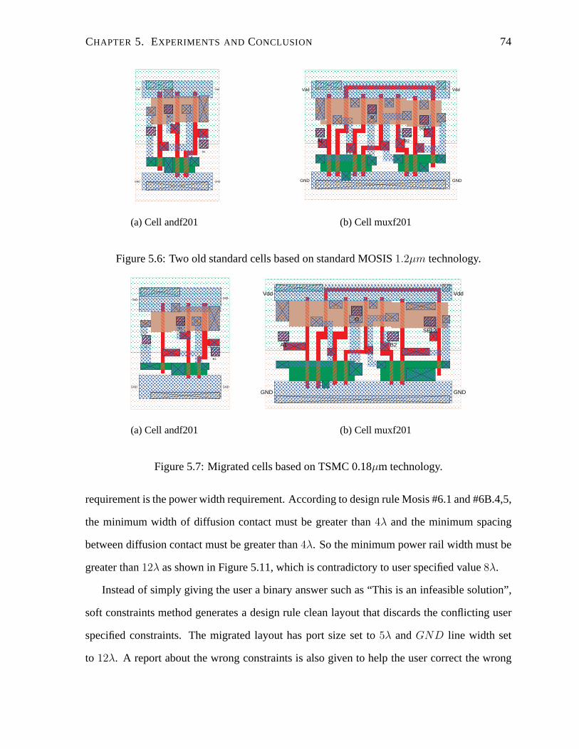
CHAPTER 5. EXPERIMENTS AND CONCLUSION 74
������������������������������������������������������������������������������������������������������������������������������������������������
������������������������������������������������������������������������������������������������
���������
���
������������
����
������
����
������
�
������
������
�������������������
����
��������
����������
�������
����������
����������
���
��������
��������
��
����
����
��
���������
������
� ����������
��
������
������
�����
�����
�����
����������
����������
���
��������
��������
������������������
����������
B1
GND
VddVdd
GND
A1
O
���������������������������������������������������������������������������������������������������������������������������������������������������������������������������������������������������������������������������������������
������������������������������������������������������������������������������������������������������������������������������������������������������������������������
����
���
��������
������������
��������
���� ��
��
����
������
����������
������
������
����
������
����������
������
������������
���������
�������������������
����
������
��������������
������
����������
������
����
��������
����
��������
��������
����
��������
����
��������
��������
��������
��������
��
�������������
����
���
����
������
����
���
����
����������
������
�����
����
������
������
���
������
��
����������
����������
��������
��
����
�� ���������������� �
��
��
��� ���� ����
��������
����
��������
����
��������
��������
����
��������
����
��������
��������
��������
��������
��
��������������������������������������
����������
����
Vdd
GND
Vdd
GND
O
SEL3
A1 B2
(a) Cell andf201 (b) Cell muxf201
Figure 5.6: Two old standard cells based on standard MOSIS1.2µm technology.
������������������������������������������������������������������������������������������������������������������������������������������������������������������������
����������������������������������������������������������������������������������������������������������������
��������
����
���������
����������
����
��������
����
������������
����������������
������
������
���������������
������
����������
����������
��
������
���
�� ����
��
���
������
������
��
����������
��
��������
����
�����
��
���
����
����������
����������
��
������
���
����������������������
������������
O
A1
B1
GND
VddVdd
GND
������������������������������������������������������������������������������������������������������������������������������������������������������������������������������������������������������������������������������������������������������������������������������
���������������������������������������������������������������������������������������������������������������������������������������������������������������������������������������������������������������������������������������������������
������
������������
��������
������������
����������
���������
������
����
���������
��������
����������
����
���������������
����
���������
������������
���������
������������������
���������
������
����������������
���������
����������������������
������
��������
������
����
��������
��������
��������
��������
��������
��������
����
����
��������
����
��������
����
�����������������
����
���
����
����
����
����
������
��������
������������
��
����
����������
������
���� ��
������
������
�
����������
�������
�����������
����
���� ���
���
������������
����
������������
����
������ ��� ���
��������
����
��������
��������
��������
��������
��������
��������
����
����
��������
����
��������
����
��������������������������������������������������
��������������
����
A1
O
B2
SEL3
GND
Vdd Vdd
GND
(a) Cell andf201 (b) Cell muxf201
Figure 5.7: Migrated cells based on TSMC 0.18µm technology.
requirement is the power width requirement. According to design rule Mosis #6.1 and #6B.4,5,
the minimum width of diffusion contact must be greater than4λ and the minimum spacing
between diffusion contact must be greater than4λ. So the minimum power rail width must be
greater than12λ as shown in Figure 5.11, which is contradictory to user specified value8λ.
Instead of simply giving the user a binary answer such as “This is an infeasible solution”,
soft constraints method generates a design rule clean layout that discards the conflicting user
specified constraints. The migrated layout has port size set to5λ andGND line width set
to 12λ. A report about the wrong constraints is also given to help the user correct the wrong
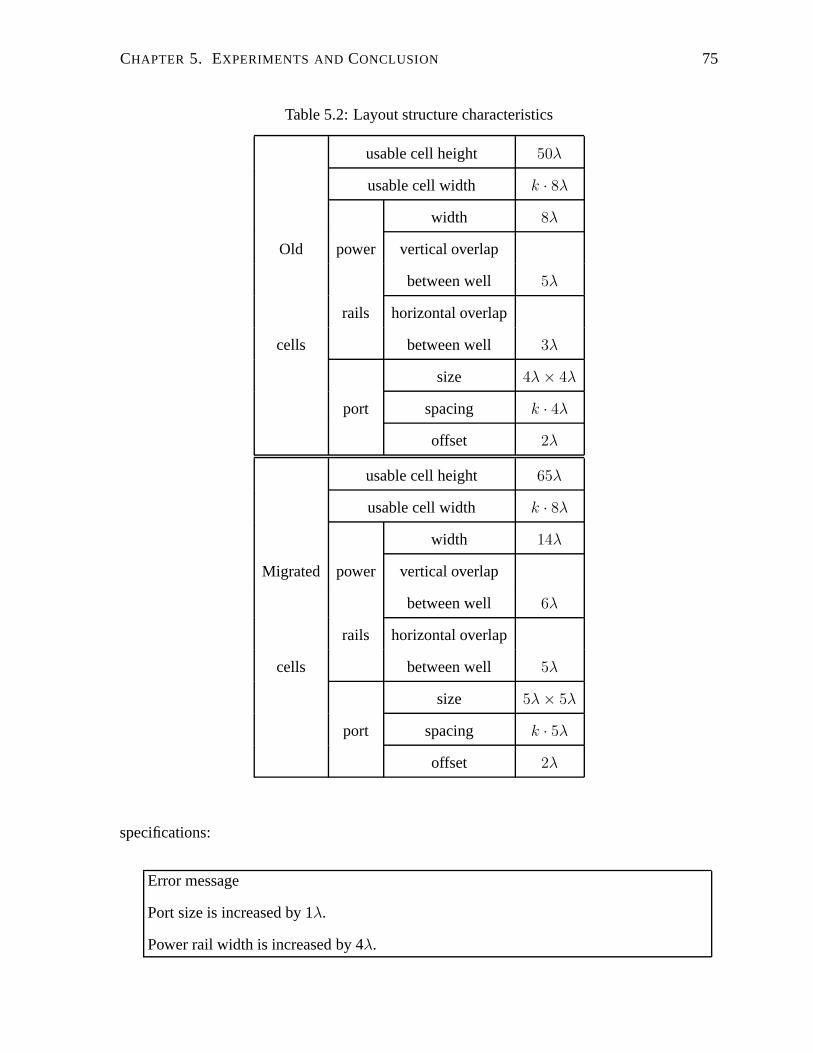
CHAPTER 5. EXPERIMENTS AND CONCLUSION 75
Table 5.2: Layout structure characteristics
usable cell height 50λ
usable cell width k · 8λwidth 8λ
Old power vertical overlap
between well 5λ
rails horizontal overlap
cells between well 3λ
size 4λ × 4λ
port spacing k · 4λoffset 2λ
usable cell height 65λ
usable cell width k · 8λwidth 14λ
Migrated power vertical overlap
between well 6λ
rails horizontal overlap
cells between well 5λ
size 5λ × 5λ
port spacing k · 5λoffset 2λ
specifications:
Error message
Port size is increased by 1λ.
Power rail width is increased by 4λ.
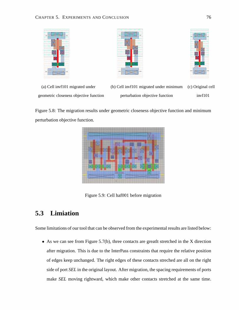
CHAPTER 5. EXPERIMENTS AND CONCLUSION 76
������������������������������������������������������������������������������������������
������������������������������������������������������������������������
������
������
���������
����������
����������
��
��
������
�����
��
����
��
����������
����������
A1 O
GND
Vdd Vdd
GND
������������������������������������������������������������������������������������������
������������������������������������������������������������������������
������������
���������
����������
����������
��
��
������
�����
��
����
��
����������
���������������
A1 O
GND
Vdd Vdd
GND
������������������������������������������������������������
������������������������������������������������
����
����
������
��������
����
������
����������
����
��
����
��������
����
����������
����
��������
��������
GNDGND
A1 O
VddVdd
(a) Cell invf101 migrated under (b) Cell invf101 migrated under minimum (c) Original cell
geometric closeness objective function perturbation objective function invf101
Figure 5.8: The migration results under geometric closeness objective function and minimum
perturbation objective function.
Figure 5.9: Cell haf001 before migration
5.3 Limiation
Some limitations of our tool that can be observed from the experimental results are listed below:
• As we can see from Figure 5.7(b), three contacts are greatlt stretched in the X direction
after migration. This is due to the InterPass constraints that require the relative position
of edges keep unchanged. The right edges of these contacts streched are all on the right
side of portSELin the original layout. After migration, the spacing requirements of ports
makeSEL moving rightward, which make other contacts stretched at the same time.
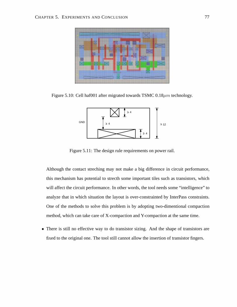
CHAPTER 5. EXPERIMENTS AND CONCLUSION 77
Figure 5.10: Cell haf001 after migrated towards TSMC 0.18µm technology.
4
4
4
12GND
Figure 5.11: The design rule requirements on power rail.
Although the contact streching may not make a big difference in circuit performance,
this mechanism has potential to strecth some important tiles such as transistors, which
will affect the circuit performance. In other words, the tool needs some “intelligence” to
analyze that in which situation the layout is over-constrainted by InterPass constraints.
One of the methods to solve this problem is by adopting two-dimentional compaction
method, which can take care of X-compaction and Y-compaction at the same time.
• There is still no effective way to do transistor sizing. And the shape of transistors are
fixed to the original one. The tool still cannot allow the insertion of transistor fingers.
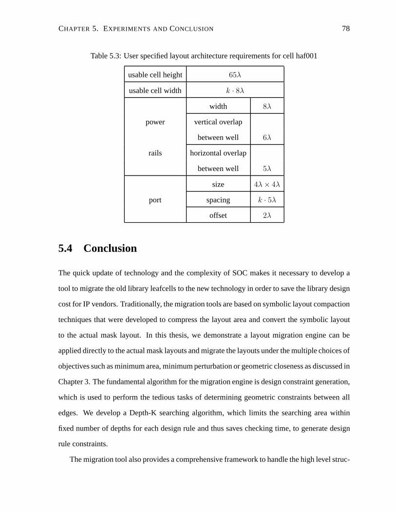
CHAPTER 5. EXPERIMENTS AND CONCLUSION 78
Table 5.3: User specified layout architecture requirements for cell haf001
usable cell height 65λ
usable cell width k · 8λwidth 8λ
power vertical overlap
between well 6λ
rails horizontal overlap
between well 5λ
size 4λ × 4λ
port spacing k · 5λoffset 2λ
5.4 Conclusion
The quick update of technology and the complexity of SOC makes it necessary to develop a
tool to migrate the old library leafcells to the new technology in order to save the library design
cost for IP vendors. Traditionally, the migration tools are based on symbolic layout compaction
techniques that were developed to compress the layout area and convert the symbolic layout
to the actual mask layout. In this thesis, we demonstrate a layout migration engine can be
applied directly to the actual mask layouts and migrate the layouts under the multiple choices of
objectives such as minimum area, minimum perturbation or geometric closeness as discussed in
Chapter 3. The fundamental algorithm for the migration engine is design constraint generation,
which is used to perform the tedious tasks of determining geometric constraints between all
edges. We develop a Depth-K searching algorithm, which limits the searching area within
fixed number of depths for each design rule and thus saves checking time, to generate design
rule constraints.
The migration tool also provides a comprehensive framework to handle the high level struc-
CHAPTER 5. EXPERIMENTS AND CONCLUSION 79
tural requirements on library leafcells so that after one migration, all library leafcells do not
need to be migrated again with respect to specific circuits. By building soft constraints for
high level structure requirements, the migration tool can give users a feedback when these
requirements are not correctly set and guide users to the successful library migration.
We conducted our experiments on the standard cell library and datapath library developed
by Burd at University of California, Berkeley. The experiments result show that the migrated
layouts are design rule clean and respect the specified structural requirements.
5.5 Future work
There is a lot of space for future work for the migration tool. An important step would be
performance characterization for the migrated layouts. Timing analysis needs to be carried out
on new layouts for performance verification. More ambitious improvements such as transistor-
sizing capability where layout topology can be changed to insert transistor fingers, as well as
extending the application to other IP libraries can be included in the extension of our work.
Chapter 6
Appendix
The tables shown in the following give more comprehensive results carried out on a SUNBlade
100 system running at 500 MHZ. Here, related cells that need port matching are migrated in
groups. The third column demonstrates two important figures,ASRis the actual area scaling
ratio achieved, as measured bymigrated layout areaold layout area
, andTSRis the linear area scaling ratio mea-
sured by(migrated feature sizeold feature size
)2, which as we know, direct layout shrinking with this ratiomay
result in design rule violations. These two values are shown for both targeted technologies.
The number of rectangles (including space) in the layout, and the total numbers of constraints
generated are shown in the fourth and fifth column. The last two columns show the runtime
spent on constraint generation ( measured in seconds ), and ILP solving ( measured in minutes
).
80
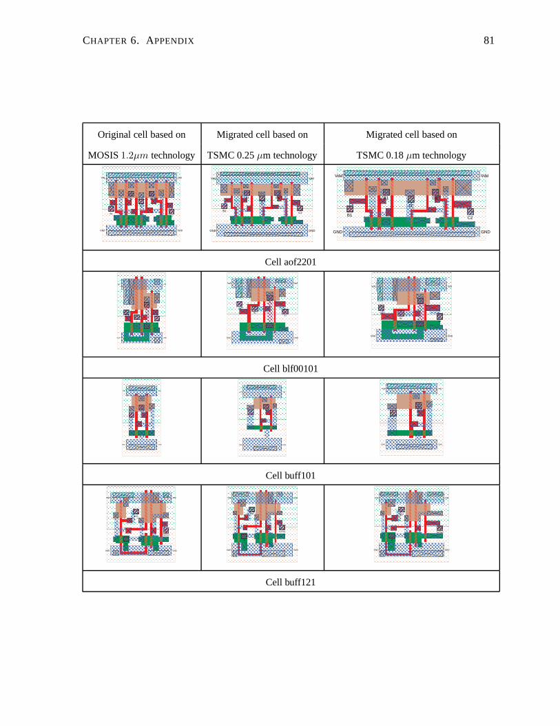
CHAPTER 6. APPENDIX 81
Original cell based on Migrated cell based on Migrated cell based on
MOSIS1.2µm technology TSMC 0.25µm technology TSMC 0.18µm technology
������������������������������������������������������������������������������������
����������������������������������������������������������������������������������������
����
�����������
������
����
����������
���������
�������������
����
������
������
���
���
���
���
������
��������
������
���� ����
�������
����
����������
�� �
�����������
�������
���
��������
��
��������
������
������
���
���
���
���
������
��������
������
����������������������
�����������
B1
Vdd
GNDGND
Vdd
A1
C2
D2
O
���������������������������������������������������������������������������������������������������������
���������������������������������������������������������������������������
��������������������������
��������
�������������
������������
������
��������������
��������
������������
������������
���
���
���
���
���
���
������
��
����
� �� �� �
����
���
����
�����������
����
�����������
������
��
���
������
��� � ��
���
���
���
���
���
���
������
��
����
������������������������
������������
B1
A1
O
D2
C2
GND
Vdd Vdd
GND
����������������������������������������������������������������������������������������������������������������������������������������������������������
��������������������������������������������������������������������������������������������������������������
����
�����������
������������������� ��
��������
����
������
��������������
��������
���������
����
����
������������������
������������
���������������
������������������
������
������
���
���
���
���
���
������
���
���
���
���
����� � � �
��������������
�����������
��������
��� ���������
����������
� ���
����
��������
���� � ��
������
������
���
���
���
���
���
������
���
���
���
���
��������������������������������������
�������������������
B1
A1
O
D2
GND
Vdd Vdd
GND
C2
Cell aof2201
�������������������������������������������������
�����������������������������������
������
���������
��
����
����
�����
��������
��������������
������
��
������
��
��
�������
�����
������
����
������
����
����
���
��������
��������������
����
������
�����
�����
������
����
������
��
�������� �
Vdd
GND
A1
C2
B2
O
Vdd
GND
������������������������������������������������������������
��������������������������������������������������
�������������
�������������
����
����
������
������
��������
��������������
������
����������
������
����
���
����
����
��
�
������
��������
��������
�������
�� ��
����
����
���
����
����
����
������ ���
C2
B2
O
A1
GND
Vdd Vdd
GND
������������������������������������������������������������������������������������
������������������������������������������������������������
���������������
������
������������
��������
�� ����������������
����
������������
������
����
����������
������
�����
��������
���
���
������
���
������
�
��
��������
������
�����������
� ���
����
��������
���
���
������
���
������
�������� ���
C2
B2
O
A1
GND
Vdd Vdd
GND
Cell blf00101
������������������������������������������
������������������������������
����
��������
��
����
����������
��������
����
���
����
��
���
�����������
������
���
���
������
���
����
��
����������
�����
GND
Vdd
GND
Vdd
O
A1
������������������������������������������
������������������������������������������
����
��������
�������
����������
���������
���
����
��
������
������
��
���
���
����
��������
����������
O
A1
GND
Vdd Vdd
GND
���������������������������������������������������������������
���������������������������������������������
��������
������
����
�������������
�������������������
���
���
��
��
��
��
�������
����
����
� �
���
���
��
��
������������
��������������
O
A1
GND
Vdd Vdd
GND
Cell buff101
����������������������������������������������������������������������
���������������������������������������������������
�����������
����
������������������
������
����
���
����������
��
��������
������������������
������
������
������
����
�����
�����
���
����
������
����
��
������
����������
�
��
������������
����
������
�����
�����
������
�����
�����
���
����
������
����
��������
���� �
GND
Vdd
GND
Vdd
EN2
DATA1
O
����������������������������������������������������������������������
��������������������������������������������������������
���������� �
����
� ��������������
����
����
�� ��
����
����������
����
����
������������������
������
��
��
�����
��
�����
�����
���
���
���
�����
����
�
���
�����
�
����������
������
��
����
��
���
��������
���
�����
�����
���
���
���
�����
����
����������
��� �
O
EN2
DATA1
GND
Vdd Vdd
GND
������������������������������������������������������������������
������������������������������������������������������������������������
���������� �
��
�� ����������������
��
���� �
����
����������
����
����
���������
��������
������
���
��
����������
�����
���
���
������
�����
������
�
���
������
�
�������������
�������
��
������
��
�����
����������
���
����������
�����
���
���
������
�����
����
����������
���� ���
O
EN2
DATA1
GND
Vdd Vdd
GND
Cell buff121
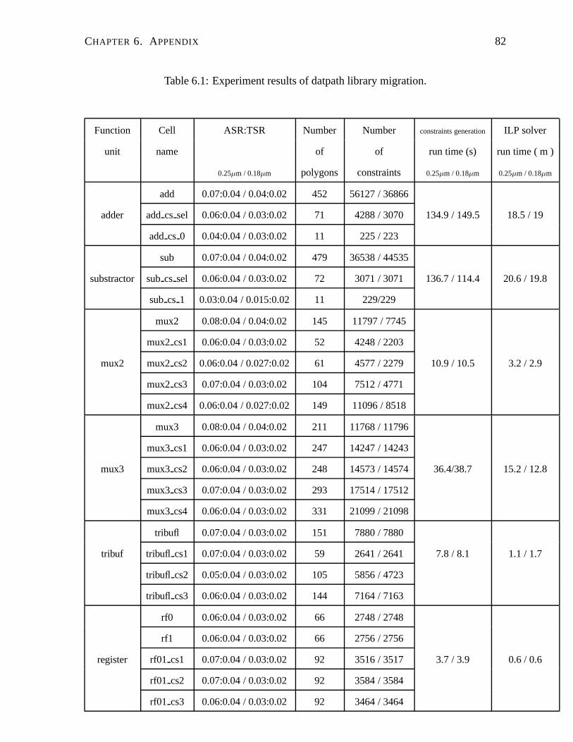
CHAPTER 6. APPENDIX 82
Table 6.1: Experiment results of datpath library migration.
Function Cell ASR:TSR Number Number constraints generation ILP solver
unit name of of run time (s) run time ( m )
0.25µm / 0.18µm polygons constraints 0.25µm / 0.18µm 0.25µm / 0.18µm
add 0.07:0.04 / 0.04:0.02 452 56127 / 36866
adder add cs sel 0.06:0.04 / 0.03:0.02 71 4288 / 3070 134.9 / 149.5 18.5 / 19
add cs 0 0.04:0.04 / 0.03:0.02 11 225 / 223
sub 0.07:0.04 / 0.04:0.02 479 36538 / 44535
substractor sub cs sel 0.06:0.04 / 0.03:0.02 72 3071 / 3071 136.7 / 114.4 20.6 / 19.8
sub cs 1 0.03:0.04 / 0.015:0.02 11 229/229
mux2 0.08:0.04 / 0.04:0.02 145 11797 / 7745
mux2 cs1 0.06:0.04 / 0.03:0.02 52 4248 / 2203
mux2 mux2 cs2 0.06:0.04 / 0.027:0.02 61 4577 / 2279 10.9 / 10.5 3.2 / 2.9
mux2 cs3 0.07:0.04 / 0.03:0.02 104 7512 / 4771
mux2 cs4 0.06:0.04 / 0.027:0.02 149 11096 / 8518
mux3 0.08:0.04 / 0.04:0.02 211 11768 / 11796
mux3 cs1 0.06:0.04 / 0.03:0.02 247 14247 / 14243
mux3 mux3 cs2 0.06:0.04 / 0.03:0.02 248 14573 / 14574 36.4/38.7 15.2 / 12.8
mux3 cs3 0.07:0.04 / 0.03:0.02 293 17514 / 17512
mux3 cs4 0.06:0.04 / 0.03:0.02 331 21099 / 21098
tribufl 0.07:0.04 / 0.03:0.02 151 7880 / 7880
tribuf tribufl cs1 0.07:0.04 / 0.03:0.02 59 2641 / 2641 7.8 / 8.1 1.1 / 1.7
tribufl cs2 0.05:0.04 / 0.03:0.02 105 5856 / 4723
tribufl cs3 0.06:0.04 / 0.03:0.02 144 7164 / 7163
rf0 0.06:0.04 / 0.03:0.02 66 2748 / 2748
rf1 0.06:0.04 / 0.03:0.02 66 2756 / 2756
register rf01 cs1 0.07:0.04 / 0.03:0.02 92 3516 / 3517 3.7 / 3.9 0.6 / 0.6
rf01 cs2 0.07:0.04 / 0.03:0.02 92 3584 / 3584
rf01 cs3 0.06:0.04 / 0.03:0.02 92 3464 / 3464
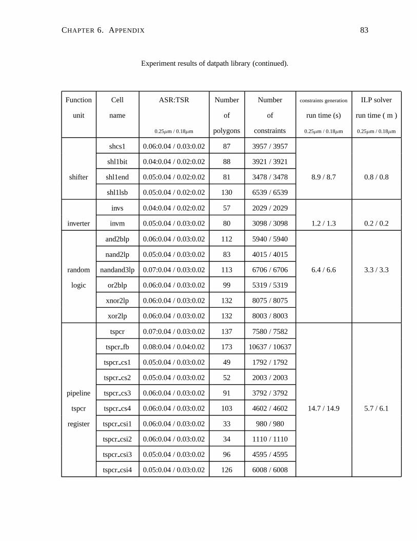
CHAPTER 6. APPENDIX 83
Experiment results of datpath library (continued).
Function Cell ASR:TSR Number Number constraints generation ILP solver
unit name of of run time (s) run time ( m )
0.25µm / 0.18µm polygons constraints 0.25µm / 0.18µm 0.25µm / 0.18µm
shcs1 0.06:0.04 / 0.03:0.02 87 3957 / 3957
shl1bit 0.04:0.04 / 0.02:0.02 88 3921 / 3921
shifter shl1end 0.05:0.04 / 0.02:0.02 81 3478 / 3478 8.9 / 8.7 0.8 / 0.8
shl1lsb 0.05:0.04 / 0.02:0.02 130 6539 / 6539
invs 0.04:0.04 / 0.02:0.02 57 2029 / 2029
inverter invm 0.05:0.04 / 0.03:0.02 80 3098 / 3098 1.2 / 1.3 0.2 / 0.2
and2blp 0.06:0.04 / 0.03:0.02 112 5940 / 5940
nand2lp 0.05:0.04 / 0.03:0.02 83 4015 / 4015
random nandand3lp 0.07:0.04 / 0.03:0.02 113 6706 / 6706 6.4 / 6.6 3.3 / 3.3
logic or2blp 0.06:0.04 / 0.03:0.02 99 5319 / 5319
xnor2lp 0.06:0.04 / 0.03:0.02 132 8075 / 8075
xor2lp 0.06:0.04 / 0.03:0.02 132 8003 / 8003
tspcr 0.07:0.04 / 0.03:0.02 137 7580 / 7582
tspcr fb 0.08:0.04 / 0.04:0.02 173 10637 / 10637
tspcr cs1 0.05:0.04 / 0.03:0.02 49 1792 / 1792
tspcr cs2 0.05:0.04 / 0.03:0.02 52 2003 / 2003
pipeline tspcr cs3 0.06:0.04 / 0.03:0.02 91 3792 / 3792
tspcr tspcr cs4 0.06:0.04 / 0.03:0.02 103 4602 / 4602 14.7 / 14.9 5.7 / 6.1
register tspcr csi1 0.06:0.04 / 0.03:0.02 33 980 / 980
tspcr csi2 0.06:0.04 / 0.03:0.02 34 1110 / 1110
tspcr csi3 0.05:0.04 / 0.03:0.02 96 4595 / 4595
tspcr csi4 0.05:0.04 / 0.03:0.02 126 6008 / 6008

CHAPTER 6. APPENDIX 84
Table 6.2: Experiment results for standard cell library migration.
Cell Number of Number of Constraint generation ILP
Name tiles constraints run time (s) run time(s)
0.25µm/0.18µm 0.25µm/0.18µm 0.25µm/0.18µm
andf201 187 4384/4378 0.3/0.3 8/14
andf301 243 6772/6264 0.6/0.6 16/27
andf401 286 7568/7578 0.7/0.8 27/40
aof2201 298 8562/8572 0.8/0.9 35/42
aof2301 410 12586/12620 1.2/1.3 73/80
aof3201 463 14930/14944 1.6/1.6 101/108
aof4201 550 18870/18888 2.5/2.5 169/199
aoif2201 241 6212/6222 0.6/0.6 18/19
blf00001 195 4233/4241 0.3/0.5 9/13
blf00101 193 4391/4379 0.5/0.5 11/15
buff101 140 2757/2761 0.3/0.3 3/6
buff102 169 3590/3594 0.3/0.3 5/8
buff103 188 4252/4257 0.3/0.4 8/10
buff104 191 4290/4294 0.4/0.4 9/11
buff105 220 5341/5345 0.5/0.5 11/18
buff106 222 5415/5419 0.5/0.5 12/19
buff121 252 6365/6371 0.6/0.6 16/25
buff122 273 7167/7173 0.6/0.6 21/36
buff123 378 11912/11918 1.2/1.6 57/95
buff124 372 12148/12154 1.2/1.4 59/74
buff125 406 13565/13571 1.5/1.6 68/83
buff126 399 13374/13380 1.3/1.6 70/83
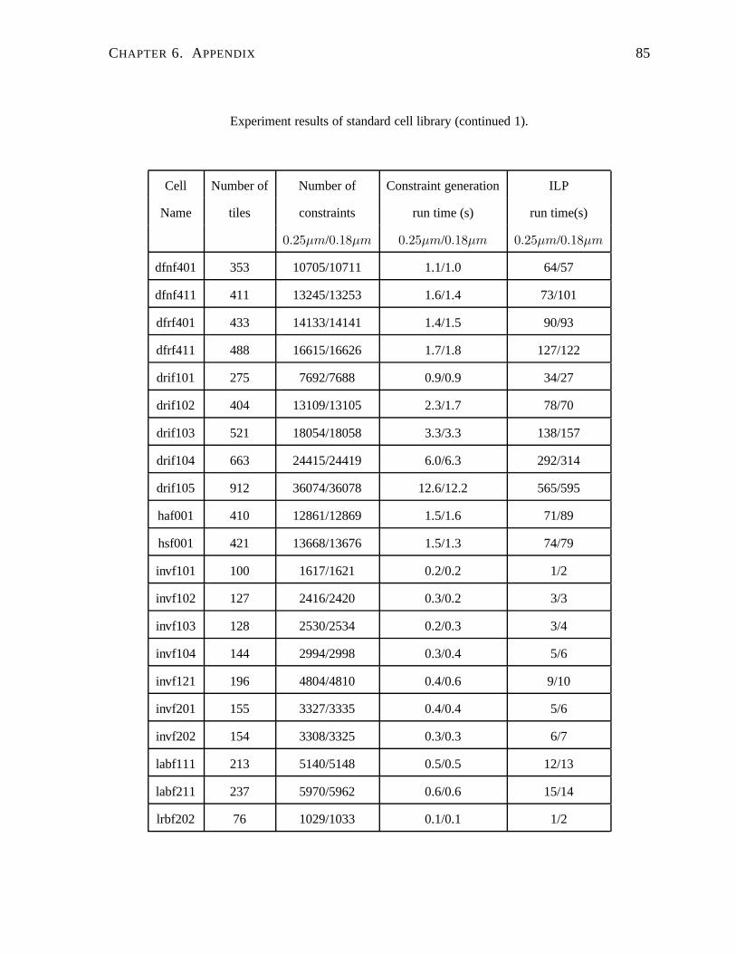
CHAPTER 6. APPENDIX 85
Experiment results of standard cell library (continued 1).
Cell Number of Number of Constraint generation ILP
Name tiles constraints run time (s) run time(s)
0.25µm/0.18µm 0.25µm/0.18µm 0.25µm/0.18µm
dfnf401 353 10705/10711 1.1/1.0 64/57
dfnf411 411 13245/13253 1.6/1.4 73/101
dfrf401 433 14133/14141 1.4/1.5 90/93
dfrf411 488 16615/16626 1.7/1.8 127/122
drif101 275 7692/7688 0.9/0.9 34/27
drif102 404 13109/13105 2.3/1.7 78/70
drif103 521 18054/18058 3.3/3.3 138/157
drif104 663 24415/24419 6.0/6.3 292/314
drif105 912 36074/36078 12.6/12.2 565/595
haf001 410 12861/12869 1.5/1.6 71/89
hsf001 421 13668/13676 1.5/1.3 74/79
invf101 100 1617/1621 0.2/0.2 1/2
invf102 127 2416/2420 0.3/0.2 3/3
invf103 128 2530/2534 0.2/0.3 3/4
invf104 144 2994/2998 0.3/0.4 5/6
invf121 196 4804/4810 0.4/0.6 9/10
invf201 155 3327/3335 0.4/0.4 5/6
invf202 154 3308/3325 0.3/0.3 6/7
labf111 213 5140/5148 0.5/0.5 12/13
labf211 237 5970/5962 0.6/0.6 15/14
lrbf202 76 1029/1033 0.1/0.1 1/2
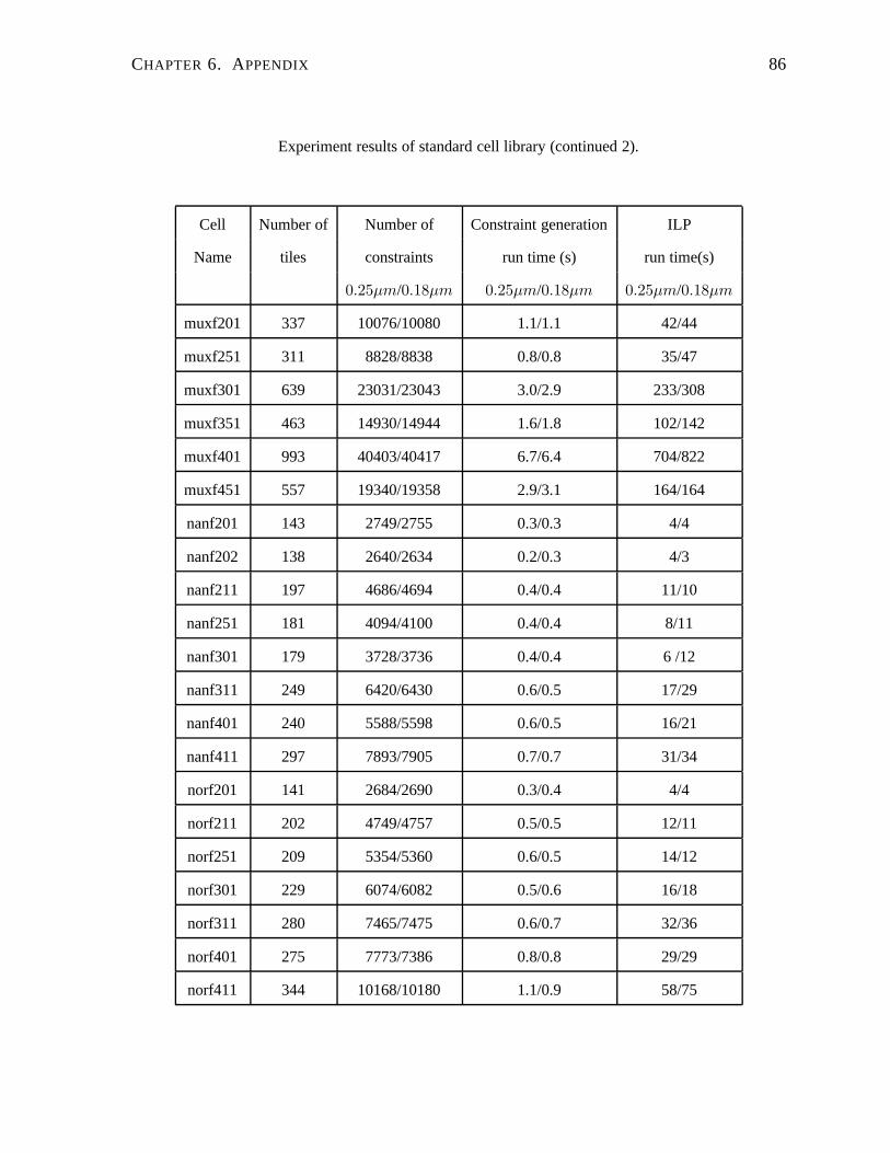
CHAPTER 6. APPENDIX 86
Experiment results of standard cell library (continued 2).
Cell Number of Number of Constraint generation ILP
Name tiles constraints run time (s) run time(s)
0.25µm/0.18µm 0.25µm/0.18µm 0.25µm/0.18µm
muxf201 337 10076/10080 1.1/1.1 42/44
muxf251 311 8828/8838 0.8/0.8 35/47
muxf301 639 23031/23043 3.0/2.9 233/308
muxf351 463 14930/14944 1.6/1.8 102/142
muxf401 993 40403/40417 6.7/6.4 704/822
muxf451 557 19340/19358 2.9/3.1 164/164
nanf201 143 2749/2755 0.3/0.3 4/4
nanf202 138 2640/2634 0.2/0.3 4/3
nanf211 197 4686/4694 0.4/0.4 11/10
nanf251 181 4094/4100 0.4/0.4 8/11
nanf301 179 3728/3736 0.4/0.4 6 /12
nanf311 249 6420/6430 0.6/0.5 17/29
nanf401 240 5588/5598 0.6/0.5 16/21
nanf411 297 7893/7905 0.7/0.7 31/34
norf201 141 2684/2690 0.3/0.4 4/4
norf211 202 4749/4757 0.5/0.5 12/11
norf251 209 5354/5360 0.6/0.5 14/12
norf301 229 6074/6082 0.5/0.6 16/18
norf311 280 7465/7475 0.6/0.7 32/36
norf401 275 7773/7386 0.8/0.8 29/29
norf411 344 10168/10180 1.1/0.9 58/75
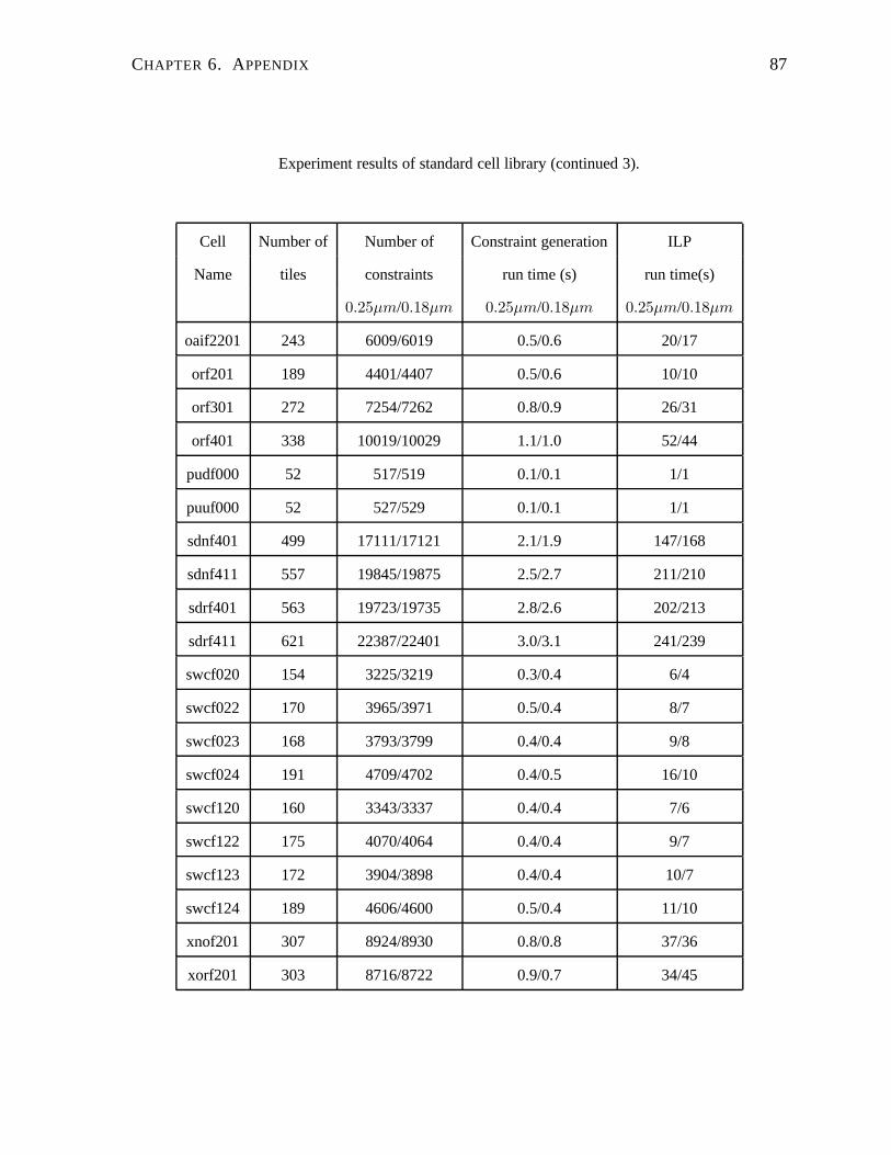
CHAPTER 6. APPENDIX 87
Experiment results of standard cell library (continued 3).
Cell Number of Number of Constraint generation ILP
Name tiles constraints run time (s) run time(s)
0.25µm/0.18µm 0.25µm/0.18µm 0.25µm/0.18µm
oaif2201 243 6009/6019 0.5/0.6 20/17
orf201 189 4401/4407 0.5/0.6 10/10
orf301 272 7254/7262 0.8/0.9 26/31
orf401 338 10019/10029 1.1/1.0 52/44
pudf000 52 517/519 0.1/0.1 1/1
puuf000 52 527/529 0.1/0.1 1/1
sdnf401 499 17111/17121 2.1/1.9 147/168
sdnf411 557 19845/19875 2.5/2.7 211/210
sdrf401 563 19723/19735 2.8/2.6 202/213
sdrf411 621 22387/22401 3.0/3.1 241/239
swcf020 154 3225/3219 0.3/0.4 6/4
swcf022 170 3965/3971 0.5/0.4 8/7
swcf023 168 3793/3799 0.4/0.4 9/8
swcf024 191 4709/4702 0.4/0.5 16/10
swcf120 160 3343/3337 0.4/0.4 7/6
swcf122 175 4070/4064 0.4/0.4 9/7
swcf123 172 3904/3898 0.4/0.4 10/7
swcf124 189 4606/4600 0.5/0.4 11/10
xnof201 307 8924/8930 0.8/0.8 37/36
xorf201 303 8716/8722 0.9/0.7 34/45
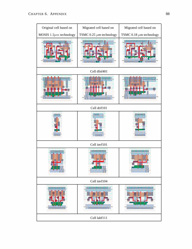
CHAPTER 6. APPENDIX 88
Original cell based on Migrated cell based on Migrated cell based on
MOSIS1.2µm technology TSMC 0.25µm technology TSMC 0.18µm technology
�������������������������������������������������������������������������������������������
�����������������������������������������������������������������
������
����������������������
����
����������
����
����������
������� ��
��
����� �� ��
���
����
����
���������������
��������� �
����
���
���������� ���
���� �
�
��������������
����������
������������
������
����
������
�� �������������
��
����
����
����
����
�����
����������������
��
���������������
�
����� �����
���
���������� ���
���� �
�
������������
��������
����������
GND
Vdd Vdd
GND
DATA1
CLK2
Q
���������������������������������������������������������������������������������������������������������
���������������������������������������������������������������������������
�������������������������
�������������������������
�������
�������
������ ������������
���������������������������
�������
���� �
���
����
��
���� ��
�� �
�
���������
�
������
��
���������������
����
�����
� ��������
��
����
������
��������������
���
�� �������������
���� �
���
����
��
���� ��
�� �
�
������������
����������
���������
DATA1
CLK2
Q
GND
Vdd Vdd
GND
���������������������������������������������������������������������������������������������������������
���������������������������������������������������������������������������
�����������������
������
����������������������������
����������
�������� ��������� �
��
��������
����������������������������
�������
�� �� �
���
����
��
������
������
���� �
�
�������������
��������
��������������
����
������
� ��������
��
��
���
���������������������
���
������������ �
�� �� �
���
����
��
������
������
���� �
�
��������������
����������
����������
DATA1
CLK2
Q
GND
Vdd Vdd
GND
Cell dfnf401
�������������������������������������������������������������������������������������������
�����������������������������������������������������������������
��������
��������
������������
����
����������
��������
����
����������
��������
�����
���
������
����������
����
�����
����������
�����
����������
����
������
������
��
������
������
�
��������������
������
��
������
��������
����
�������
������
�����
����������
�����
����������
����
������
������
����
����
��������
���
����������������������
���������� �����
�����
�� �
GND
Vdd
GND
Vdd
A1O
������������������������������������������������������������������������������
������������������������������������������������������������������������������
�����������������������
����
��������
������������
��������������
��������
������������
��
������
��
�����
�����
�����
�����
������
����������
����
��
����������������
���
���
���
������
�������
��������
�����
�����
�����
�����
������
������������ �
��������
���
��������������������
����������
����������
����
�� �
O A1
GND
Vdd Vdd
GND
���������������������������������������������������������������������������������������������������������
���������������������������������������������������������������������������
������
������
������
������
�������������
��
��������
������������
������
����������
������
����������
����
��������
����
�����
�����
�����
����������
���
���
���
���
��������
����������
��
�������������������
������������
������
�����
�����
�����
����������
���
���
���
���
���������� �
����������
����
��������������������������
����������
������������
����
�� �
O A1
Vdd Vdd
GND GND
Cell drif101
����������������������������
��������������������
����
����
������
�����
����
��������
����
��
�������
��
��������
����
��������
����
GNDGND
A1 O
VddVdd
������������������������������������������
�����������������������������������
����
����������
�������
�
�
�������
�
���
�
��������
������
A1 O
GND
Vdd Vdd
GND
������������������������������������������
������������������������������������
����������������
�
�
������
��
��
�
����������
����������
A1 O
GND
Vdd Vdd
GND
Cell invf101
�������������������������������������������������
�����������������������������������
��
����������
������
��������
������������
���
��
��������
����
��������
����
��
�����
�����������������
����
��
����
��
��������
����
��������
����
��
��������
������
Vdd
GND GND
Vdd
OA1
��������������������������������������������������������
����������������������������������������
������������
������
���
������
�����������
���
��������
���
���
������
��� �
������
��
������
������
���
���
������
���
���
������
������������
������������
A1 O
Vdd Vdd
GNDGND
���������������������������������������������������������������
���������������������������������������������
����������
������
������
������������
������
������������
���
��
����
��������
��������
������
�����
�����������
����������
������
���
����
��������
��������
������
��������
��������
A1 O
Vdd Vdd
GND GND
Cell invf104
���������������������������������������������������������������
�������������������������������������������������������������
��������
������
�����
����������
����
����������
��������
���
������
���
����������
������
�������
���������
���������������
�����
����
����������
������
���
������
���
����������
����������������
��������
Vdd
GND
Vdd
GND
SET2 RST1
Q_bQ
������������������������������������������������������������������������������������
������������������������������������������������������������
��������������������������
����
������������
������������������
��������
��
����
���
���
���
���
��������
������
��
���������
���������
����
����
����
���
���
���
���
��������
��������������������
���������
SET2
Q Q_b
RST1
GND
Vdd Vdd
GND
�������������������������������������������������������������������������������������������
�����������������������������������������������������������������������������������������
����
�������������
����
������������
���������
���
��
���
������
���
������
������
������
���� ��
����������������������
����������������
������
���
������
���
������
������
������
������������������������
������������
SET2
Q Q_b
RST1
GND
Vdd Vdd
GND
Cell labf111
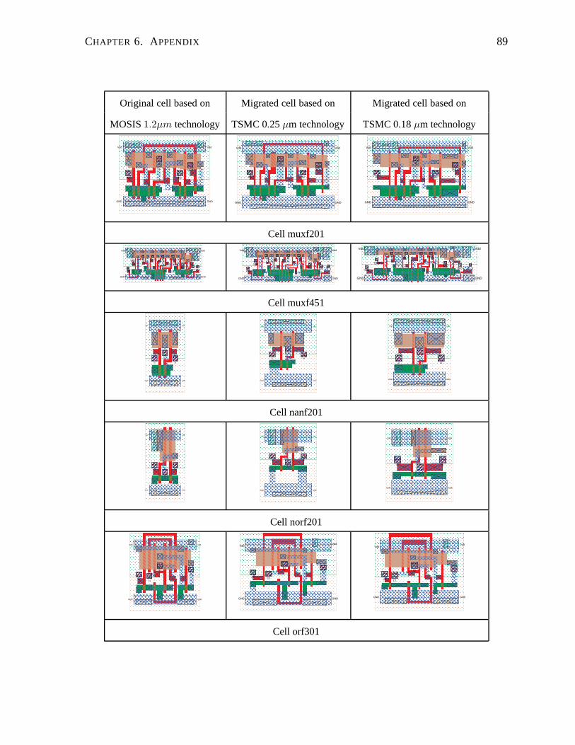
CHAPTER 6. APPENDIX 89
Original cell based on Migrated cell based on Migrated cell based on
MOSIS1.2µm technology TSMC 0.25µm technology TSMC 0.18µm technology
�������������������������������������������������������������������������������������������
���������������������������������������������������������������������������
�������� ���� ��
������������
��
������
�������
��������������
������
������������
���������������
��������
����
���
���
���
���
������
���
������������
�������
�����������
�� �����
�
���������
����
����
�������
���� �
��
���
�����������
����
����
��
������������
��
��
������������
������
������
���
���
���
���
������
���
������������
�������
������������������������
���� ��
Vdd
GND
Vdd
GND
O
SEL3
A1 B2
���������������������������������������������������������������������������������������������������������
����������������������������������������������������������������������������������������������������� �
������������
��
������
������
��������������
������������������
������������������
�������
��
���
������
���
���
���
���
��������
������ �
��������������� �� �
�
����
�������������
�������
��
��
��
��������
����� �����
�� ��
�����������
��
������ ���
���
���
������
���
���
���
���
��������
������ �
������������������������
������
��
A1
O
B2
SEL3
GND
Vdd Vdd
GND
���������������������������������������������������������������������������������������������������������
���������������������������������������������������������������������������������
�������������� ��
���������������
��
������
������
����
��������������
����������������
������������������
��������
����
���
������
���
���
������
���
����������������
������ �
������������������� �
�
����
���������������������
������������ �
����
�����������
��������
��
���� ��
����������
����
��
������������ ���
������
���
������
���
���
������
���
����������������
������ �
����������������������������
����� �
A1
O
B2
SEL3
GND GND
Vdd Vdd
Cell muxf201
��������������������������������������������
������������� ��
���������������������������������
����
����
�����������������������������������
��
�����������������������������������������������������
���
���������������������
����
������������� �����
�����������
�������
�������������������������
��������
��������������������
������
��������
����
������������
��������������������������������
������
����������������������
����
������������� �����
�� ��� ��
���� ��
����
Vdd
GNDGND
Vdd
O
IN0
S_0
IN1 S_1 IN2
S_2IN3 S_3 �������������
���������������������������������������
��� ������������ ��
���������������������������������������� ��������������
����������������
������������
���������������������������������������������������������
���������������������������
�������������� �����
������������
��������������������������������������
���������������
������������
���������
������������������
������������������
����������������������������
�������������� �����
�� ��� ����
������
������
������
IN0
S_0
IN1 S_1 O IN2
S_2IN3 S_3
GND
Vdd Vdd
GND
������������������������������������������������
��������
����������
������������
������
����
������������������������������������������������� �����������
����������
�������
������
��������
�����������������
�������
��
�������������������������������������������������
���������������
����������
���
���
���
�������
����
����������������������
�����������������������������
������
��� �����������
��������������
����������
����
��� ��������������
����
�����������
���������������
����������
���
���
���
�������
����
�� ��� ����
����
����
���������
IN0
S_0
IN1 S_1 O
S_2IN3 S_3
GND
Vdd Vdd
GND
IN2
Cell muxf451
������������������������������������������
������������������������������������
��������
������
����
����������
������
���
������
���
�
��������
���������
������
������
���
������
����������
�����
VddVdd
GND GND
O
B1A1
������������������������������������������������
������������������������������������������������������
��������
������
����
�������������
������
���
������
���
����
������
��������
�����
���
������
���
������
������������
������������
A1
O
B1
GND
Vdd Vdd
GND
���������������������������������������������������������������
���������������������������������������������������������
����������
������������
����
�������������
���
������
����
���
���
����
�������������
��
���
������
����
����������������
����������������
A1
O
B1
GND
Vdd Vdd
GND
Cell nanf201
������������������������������������������
��������������������������������������������������
������
������
����������
��������
�����������
�����
����
��
����
���
��������
���
����
���
�����
�����
����
��
����������
������
VddVdd
GND GND
A1
O
B1
������������������������������������������������
���������������������������������������������������������
������������
��������
������������
��������
������������
�����
����
��
��
���������
�����
���
�����
�����
����
��
������������
��������
A1
O
B1
GND
Vdd Vdd
GND
������������������������������������������������������������
������������������������������������������������������������
����������������
����������������
������
������������
��������
������
����
����
��
��
����
����
��������
���
������
� �
����
����
��
��
������������������
���������
A1
O
B1
GND
Vdd Vdd
GND
Cell norf201
����������������������������������������������������������������������
������������������������������������������������������������������
��
���� ��
������
����
��
����
����
������������
������
����
�����������
����������
����
��������
����
����
��������
����
����
���
����
������
��
������
��������������
�������������
�
����������������
������
����������
���
�����
������
������
�����
��������
����
����
��������
����
����
���
����
������
��
��������
������
�
Vdd
GND
Vdd
GND
A1
B1
C1
O
��������������������������������������������������������������������������������������������������
��������������������������������������������������������������������������������������
��������
������ ��
��������
����
��
������
������
����������
����������
���������
������
������
����
�����
���
���
���
���
���
���
��
����
��
������
����������������
�
�������������������������
������
�
����
���������
�
��������
���
���
���
���
���
���
���
��
����
��
��������
��������
����
A1 C1
B1
O
GND
VddVdd
GND
�������������������������������������������������������������������������������������������
������������������������������������������������������������������������������
��� �����
��
����
��������
������������
������
���
�����������
������
���
�����������
���
���
���
������
���
���
�� � � �
�������
�������������� ���
�����
�
��������������
��
����������
��
�����������
�����
��� �
������
����
�
����
������
���
���
���
������
���
���
�� � � �
��������
��������
����
A1 C1
B1O
GND
VddVdd
GND
Cell orf301
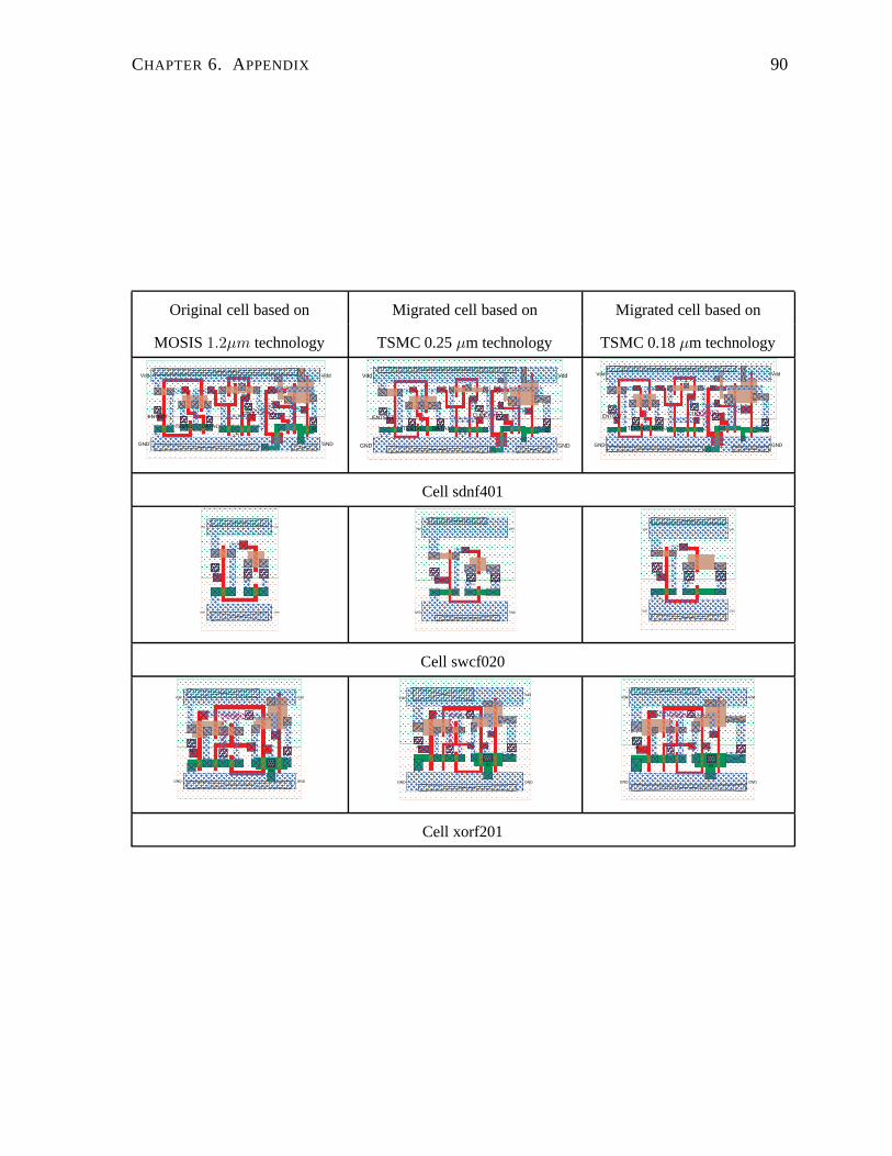
CHAPTER 6. APPENDIX 90
Original cell based on Migrated cell based on Migrated cell based on
MOSIS1.2µm technology TSMC 0.25µm technology TSMC 0.18µm technology
������������������������������������������������������������������������������������������������
���������������������������������������������������������������������
��������������
����������� ���������
�������
��������
������������
���������� ��
�������������
������
������������������������
�����
�
������ �
�����
��
����
���
����
� ��������
��� ����
�� �
�����������
��������� ���
������
����
���
��� �������
�������
�������
� ���� ����
���
����
���
� ���� ���������
��
����
��
���������������
���
�������� �����
��������
��
��
������ �
�����
��
����
���
����
� ��������
��� ����
�� �
����������������������
��������
��������������
Vdd
CLK2
Q
Vdd
ENTEST
TESTin DATA1
GND GND
������������������������������������������������������������������������������������������������������������
�������������������������������������������������������������������������������������������������������
����
����������
������
��������������������������� ��
������� �
�������
��
���������������������������
��������
�
�������� �
���
����
� �� ���� ������� �
���������������� ����������
������
������ �����
�����
������
��������
������
����
����
� �� �����������
�����
����������������
���
������ ������
��������
��
�������� �
���
����
� �� ���� ������� �
��������������������
��������
����������������������������
ENTEST
TESTin DATA1
CLK2
Q
GND
Vdd Vdd
GND
������������������������������������������������������������������������������������������������
����������������������������������������������������������������������������������������������
��
�������
�������������������������
����� ��
�����������
������
�������������������
������
�
����
��� �
������
����
� �� ��� ����� �
������������
����
��������
���
��� �
�
��
�����
�������
������
� ����
����
���
����
���
� �� �������
������
�����������������������
���
������ �����
��������
��
����
��� �
������
����
� �� ��� ����� �
��������������������
����������
��������������������������
ENTEST
TESTin DATA1
CLK2
Q
GND
Vdd Vdd
GND
Cell sdnf401
�������������������������������������������������
������������������������������������������
����
����
��
�����
�
����
��
������
�� ��
��������
��
��������
��
����
����
����
�����
����
������
�� ��
������������
������
GND
Vdd
GND
Vdd
CTL2
DATA1 O ���������������������������������������������������������������
�����������������������������������������������������
���������������
����
�� �
����
�������
����������
�
�����
��
����
����
�� �
��������������
������������
CTL2
DATA1 O
GND
Vdd Vdd
GND
���������������������������������������������������������������
�������������������������������������������������������
������
����
������
����
��
����
� ��
���������
��������
��������
����
��
����
� ��
����������������
��������
CTL2
DATA1 O
GND
Vdd Vdd
GND
Cell swcf020
������������������������������������������������������������������������������������
������������������������������������������������������������
����������������������
�����������
�����
��
���
����
�������������� ����������
����������
��
�����
�����
���� �
���������
����
����
������
�������
������
�� ��
���������
��
������ ��
��������
��� �
�������
���� �������
����
���� �
���������
����
����
������
����������������������
��������
Vdd Vdd
GNDGND
O
B1
A1 ������������������������������������������������������������������������������������
������������������������������������������������������������������
�����������������
����������
����������
����
����
���������
������
����
���������������
��������
�����
������
���� �
����
����������
���
���
��
��������������� ���
�������� �
�����
���������� �
���
�� ����
����������
������
���
������
���� �
����
����������
���
���
��������������������
������������
A1
B1
O
GND
VddVdd
GND
������������������������������������������������������������������������������������
������������������������������������������������������������
����
����������������
����������
���������
����
������
������������
��������
����
����
���������������
������
�����
���
���� �
����
�������
���
��
�������������� �
����
�������� �
�����
������
�� ��
����
���� ��
��
��������
������
���
���
���� �
����
�������
���
������������������������
�������
A1
B1
O
GND GND
Vdd Vdd
Cell xorf201

CHAPTER 6. APPENDIX 91
Original cell based on Migrated cell based on Migrated cell based on
MOSIS1.2µm technology TSMC 0.25µm technology TSMC 0.18µm technology
������������������������������������������������������������������������������������������������������������������������������������������������������������������������������������������������������������������������������������������������������������
������������������������������������������������������������������������������������������������������������������������������������������������������������������������������������
���������������������������������������
������
������������������
���������������������
���������������������������
������
���������
�����������������������������
������
������������
���������������������
�����������������������������������
�����������������������������������
��������������
����������������������
����������������
�����������������������������������
�����������������������������������
�������������������������������������
�����������������������
���������������������
�����������������������������������
�������������������������������������
�����������������������
��������������
�����������������������������������
�������������������������������������
����������������������������������������
����������
�����������������������������������
����������
��������������
����������������������������
����������
��������������
����������������������������
������
������
������
���
������
������
������
������
���������
������
������
������������
������
������
� ������ �� ������� ��
��
� ������
����
�� ������
����
�� ����� ���� �
������
��
�������� �
� ������� ����
� ������
����
�� ������
����
�� ������
����
�� �
������
��
�������� �
��
�������� ����
� ���� ����
� ������
����
�� ������
����
�� �
������
��
�������� �
��
�������� ���
� ���� ����
� ���� ����
� ������
����
�� �
����������������������������������������
����������
�����������������������������������
����������
��������������
����������������������������
����������
��������������
����������������������������
������
������
������
���
������
������
������
������
���������
������
������
������������
������
��������
���
��������
������
��������
������
��������
������
������
������
������
������
bufh
bufh_3
bufh
bufh_2
bufh
bufh_1
bufh
bufh_0
INVdd
Vdd
OUT
FEED5
FEED4
FEED3
FEED2
GND
GNDIN
OUT
FEED1
FEED2
FEED3
FEED4
FEED5
INVdd
Vdd
OUT
FEED5
FEED4
FEED3
FEED2
GND
GNDIN
OUT
FEED1
FEED2
FEED3
FEED4
FEED5
INVdd
Vdd
OUT
FEED5
FEED4
FEED3
FEED2
GND
GNDIN
OUT
FEED1
FEED2
FEED3
FEED4
FEED5
INVdd
Vdd
OUT
FEED5
FEED4
FEED3
FEED2
GND
GNDIN
OUT
FEED1
FEED2
FEED3
FEED4
FEED5
������������������������������������������������������������������������������������������������������������������������������������������������������������������������������������������������������������������������
������������������������������������������������������������������������������������������������������������������������������������������������
�����������
���������������������������
�����������
���������������������������
��������������������������������������
������������������������������������
�����������������
������������
������������������������������������������������
������������
�������������������
�����������������
������������������������������
������������������������������
��������������������������������
�����������������
������������������������������
������������������������������
��������������������������������
�������������
������������������������������
������������������������������
��������������������������������
����������������������������������
����������������������������������
����������������������������������
��������
������������������������������
��
������������
������
��
���������
���������
��
������
������������
��
���������������
���
� ������� �
������� ��� �
���� ��� ������
��
�� ������
��
�� �
���
� ������� �
������� ��� ��
����
��
�� ������
��
�� ���� ���
� �
���
� ������� �
������
�� ��
�� ������
��
�� ���� ���
� ���� ���
� �
���
��
�������
� ������ �
��� ���� ��� ���� ���
� ���� ���
� �
����������������������������������
����������������������������������
����������������������������������
��������
������������������������������
��
������������
������
��
���������
���������
��
������
������������
��
���������������
���
���
������
������
������
������
������
������
��
����
����
����
bufh_mig
bufh_mig_3
bufh_mig
bufh_mig_2
bufh_mig
bufh_mig_1
bufh_mig
bufh_mig_0
Vdd GND
Vdd GND
OUT
FEED5
FEED4
FEED3
FEED2
FEED1IN
OUT
FEED5
FEED4
FEED3
FEED2
IN
Vdd GND
Vdd GND
OUT
FEED5
FEED4
FEED3
FEED2
FEED1
IN
OUT
FEED5
FEED4
FEED3
FEED2
IN
Vdd GND
Vdd GND
OUT
FEED5
FEED4
FEED3
FEED2
FEED1IN
OUT
FEED5
FEED4
FEED3
FEED2
IN
Vdd GND
Vdd GND
OUT
FEED5
FEED4
FEED3
FEED2
FEED1
IN
OUT
FEED5
FEED4
FEED3
FEED2
IN
������������������������������������������������������������������������������������������������������������������������������������������������������������������������������������������������������������������������
������������������������������������������������������������������������������������������������������������������������������������������������
�����������
���������������������������
�����������
���������������������������
��������������������������������������
������������������������������������
�����������������
������������
������������������������������������������������
������������
�������������������
�����������������
������������������������������
������������������������������
��������������������������������
�����������������
������������������������������
������������������������������
��������������������������������
�������������
������������������������������
������������������������������
��������������������������������
����������������������������������
����������������������������������
����������������������������������
��������
������������������������������
��
������������
������
��
���������
���������
��
������
������������
��
���������������
���
� ������� �
������� ��� ����� ��� ������
��
�� ������
��
�� �
���
� ������� �
������� ��� ������
��
�� ������
��
�� ���� ���
� �
���
� ������� �
�������� �
��� ������
��
�� ���� ���
� ���� ���
� �
���
��
�������
� ������ �
��� ���� ��� ���� ���
� ���� ���
� �
����������������������������������
����������������������������������
����������������������������������
��������
������������������������������
��
������������
������
��
���������
���������
��
������
������������
��
���������������
���
���
������
������
������
������
������
������
��
����
����
����
bufh_mig
bufh_mig_3
bufh_mig
bufh_mig_2
bufh_mig
bufh_mig_1
bufh_mig
bufh_mig_0
Vdd GND
Vdd GND
OUT
FEED5
FEED4
FEED3
FEED2
FEED1IN
OUT
FEED5
FEED4
FEED3
FEED2
IN
Vdd GND
Vdd GND
OUT
FEED5
FEED4
FEED3
FEED2
FEED1
IN
OUT
FEED5
FEED4
FEED3
FEED2
IN
Vdd GND
Vdd GND
OUT
FEED5
FEED4
FEED3
FEED2
FEED1IN
OUT
FEED5
FEED4
FEED3
FEED2
IN
Vdd GND
Vdd GND
OUT
FEED5
FEED4
FEED3
FEED2
FEED1
IN
OUT
FEED5
FEED4
FEED3
FEED2
IN
A four-bit buffer with high drive length
������������������������������������������������������������������������������������������������������������
������������������������������������������������������������������������������������������������������������������������������������������������
����
����
�������������
����
����
�������������
����
����
��������������
����
����
��������������
����������������
�������������������
���������
����������
���������������
�������������������
��������������������
�������������
�������������������
��������������������
�������������
�������������������
��������������������
����
���������
����
���������
����
���������
����
�����������
������
������
������
������
����������
������ ���
������
��
� �����
� �
����������
������ ���
������
��
� �����
� �
����������
������ ���
������
��
� �����
� �
����
���������
������ ���
������
��
� �����
� �
����
���������
����
���������
����
���������
����
�����������
������
������
������
������
����������
������
����������
������
��������
������
��������
������
������
���
������
���
������
������
������
������
bufm
bufm_3
bufm
bufm_2
bufm
bufm_1
bufm
bufm_0
Vdd
Vdd GND
GNDIN IN
OUTOUT
FEED5
FEED4
FEED3
FEED2
FEED1 FEED1
FEED2
FEED3
FEED4
FEED4
Vdd
Vdd GND
GNDIN IN
OUTOUT
FEED5
FEED4
FEED3
FEED2
FEED1 FEED1
FEED2
FEED3
FEED4
FEED4
Vdd
Vdd GND
GNDIN IN
OUTOUT
FEED5
FEED4
FEED3
FEED2
FEED1 FEED1
FEED2
FEED3
FEED4
FEED4
Vdd
Vdd GND
GNDIN IN
OUTOUT
FEED5
FEED4
FEED3
FEED2
FEED1 FEED1
FEED2
FEED3
FEED4
FEED4
������������������������������������������������������������������������������������������������������������
������������������������������������������������������������������������������������������������������������
������
�����������
������
�����������
����
����
�������������
����
����
�������������
�����������������������������
�������������������������������
������������������������
���������
������������������������
������������
������
����
����
����������
����������
����������
����
����
������
������
������
��������������������
��
������
��
�����
����������������������
��
�������
����������������������
��
��������
������������������������
��
��������
������
����
����
����������
����������
����������
����
����
������
������
������
����������
���
����������
������
����������
������
����������
������
��
��
����
��
����
��
����
��
bufm_mig
bufm_mig_3
bufm_mig
bufm_mig_2
bufm_mig
bufm_mig_1
bufm_mig
bufm_mig_0
Vdd GND
Vdd GND
FEED4OUTFEED4FEED3FEED2FEED1
IN
FEED5OUT
FEED4FEED3FEED2FEED1
IN
Vdd GND
Vdd GND
FEED4OUTFEED4FEED3FEED2FEED1
IN
FEED5OUT
FEED4FEED3FEED2FEED1
IN
Vdd GND
Vdd GND
FEED4OUTFEED4FEED3FEED2FEED1
IN
FEED5OUT
FEED4FEED3FEED2FEED1
IN
Vdd GND
Vdd GND
FEED4OUTFEED4FEED3FEED2FEED1
IN
FEED5OUT
FEED4FEED3FEED2FEED1
IN
������������������������������������������������������������������������������������������������������������
������������������������������������������������������������������������������������������������������������
������
�������
����
������
�������
����
����
����
�������
������
����
����
���������
����
�����������������������������
�������������������������������
������������������������
���������
������������������������
������������
������
����
����
����������
����������
����������
����
����
������
������
������
����������������������
������
��
�����
������������������������
�������
������������������������
��������
��������������������������
��������
������
����
����
����������
����������
����������
����
����
������
������
������
����������
���
����������
������
����������
������
����������
������
��
��
����
��
����
��
����
��
bufm_mig
bufm_mig_3
bufm_mig
bufm_mig_2
bufm_mig
bufm_mig_1
bufm_mig
bufm_mig_0
Vdd GND
Vdd GND
FEED4OUTFEED4FEED3FEED2FEED1
IN
FEED5OUT
FEED4FEED3FEED2FEED1
IN
Vdd GND
Vdd GND
FEED4OUTFEED4FEED3FEED2FEED1
IN
FEED5OUT
FEED4FEED3FEED2FEED1
IN
Vdd GND
Vdd GND
FEED4OUTFEED4FEED3FEED2FEED1
IN
FEED5OUT
FEED4FEED3FEED2FEED1
IN
Vdd GND
Vdd GND
FEED4OUTFEED4FEED3FEED2FEED1
IN
FEED5OUT
FEED4FEED3FEED2FEED1
IN
A four-bit buffer with medimum drive length
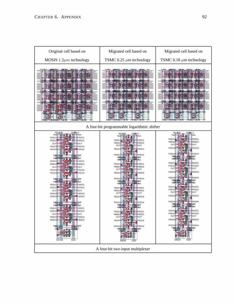
CHAPTER 6. APPENDIX 92
Original cell based on Migrated cell based on Migrated cell based on
MOSIS1.2µm technology TSMC 0.25µm technology TSMC 0.18µm technology
������������
��������������������
����������������
���������������
�������������������������
��������������������
���������������
�������������������������
��������������������
������������
��������������������
����������������
���������
���������������
������������
��������
��������
����������������
������������
����������
����������
��������������������
���������������
����������
����������
��������������������
���������������
��������
��������
����������������
������������
������
������
������������
���������
����
����
���
����
���
���� ��
�� ��
����� ��
�
���
��� �
���
��� �
���
��������
��������
����
��������
����
�����
�����
�����
���� �
���
��� �
���
���
����
����
���
����
���
���� ��
�� �
��� ��
�� �
���
��������������
��������������
����
��������������
��
����
��������������
��������������
�����������
������������
�� �� ��� �� �
��
��
��
��� �
����
�� �� �� �� ��
����
����
��
�����
��
����
����
��������
��
�� �
��
�� �
��
�� �� ��� �� �
��
��
�� ��
�� ��
����
����
��
����
��
��
��
��
�������������������
�������������������
����������������
���������������������
���������������������
�����
�������������������
�������������������
��
��������������� ����������
����������
����������������������
������
����������������
������
����������������
��������������
������
��������������
����
�����������������
������� �
����������������������������
������
������� �
����������������������������
������
��������������
������� �
�����������������������
�����
��������������������
��������������������
��������������������
���������������
�� �� ��� �� �
��
��
��
��� �
����
�� �� �� �� ��
����
����
��
�����
��
����
����
��������
��
�� �
��
�� �
��
�� �� ��� �� �
��
��
�� ��
�� ��
����
����
��
����
��
��
��
��
������
���� ��
����
����
����
���
��
����
������
���� ��
����
����
����
���
��
����
������
��������
�� ����
���
� ����
��������
�� ��������
�� ����
����
� ����
������
������
���
��
�����
��
�����
����
��
���������
�����
��
�����
��
����
�����
������
��
����
��
����
����
��
��������
�����
����� �
��� �
��������
������
������
���
shl1bit
shl1bit_4
shl1bit
shl1bit_7
shlbuf1
shlbuf1_3
shl1bit
shl1bit_11
shlbuf1
shlbuf1_7
shl1bit
shl1bit_3
shl1bit
shl1bit_6
shlbuf1
shlbuf1_2
shl1bit
shl1bit_10
shlbuf1
shlbuf1_6
shl1bit
shl1bit_2
shl1bit
shl1bit_5
shlbuf1
shlbuf1_1
shl1bit
shl1bit_9
shlbuf1
shlbuf1_5
shl1lsb
shl1lsb_0
shl1lsb
shl1lsb_1
shlbuf1
shlbuf1_0
shl1lsb
shl1lsb_2
shlbuf1
shlbuf1_4
shcs1
shcs1_0
shcs1
shcs1_1
shpwr1shpwr1_1
shcs1
shcs1_2
shpwr1shpwr1_0
GND
GND SBAR1S1
SBAR1S1
Vdd
VddNEXT1
PREV1
INFEED1
FEED2FEED3FEED4FEED5FEED6 FEED6
FEED5FEED4FEED3FEED2
FEED1OUT
GND
GND SBAR1S1
SBAR1S1
Vdd
VddNEXT1
PREV1
INFEED1
FEED2FEED3FEED4FEED5FEED6 FEED6
FEED5FEED4FEED3FEED2
FEED1OUT
GND
GND
Vdd
Vdd
FEED2FEED3FEED4FEED5FEED6
FEED1IN
FEED6FEED5FEED4FEED3FEED2
FEED1OUT
GND
GND SBAR1S1
SBAR1S1
Vdd
VddNEXT1
PREV1
INFEED1
FEED2FEED3FEED4FEED5FEED6 FEED6
FEED5FEED4FEED3FEED2
FEED1OUT
GND
GND
Vdd
Vdd
FEED2FEED3FEED4FEED5FEED6
FEED1IN
FEED6FEED5FEED4FEED3FEED2
FEED1OUT
GND
GND SBAR1S1
SBAR1S1
Vdd
VddNEXT1
PREV1
INFEED1
FEED2FEED3FEED4FEED5FEED6 FEED6
FEED5FEED4FEED3FEED2
FEED1OUT
GND
GND SBAR1S1
SBAR1S1
Vdd
VddNEXT1
PREV1
INFEED1
FEED2FEED3FEED4FEED5FEED6 FEED6
FEED5FEED4FEED3FEED2
FEED1OUT
GND
GND
Vdd
Vdd
FEED2FEED3FEED4FEED5FEED6
FEED1IN
FEED6FEED5FEED4FEED3FEED2
FEED1OUT
GND
GND SBAR1S1
SBAR1S1
Vdd
VddNEXT1
PREV1
INFEED1
FEED2FEED3FEED4FEED5FEED6 FEED6
FEED5FEED4FEED3FEED2
FEED1OUT
GND
GND
Vdd
Vdd
FEED2FEED3FEED4FEED5FEED6
FEED1IN
FEED6FEED5FEED4FEED3FEED2
FEED1OUT
GND
GND SBAR1S1
SBAR1S1
Vdd
VddNEXT1
PREV1
INFEED1
FEED2FEED3FEED4FEED5FEED6 FEED6
FEED5FEED4FEED3FEED2
FEED1OUT
GND
GND SBAR1S1
SBAR1S1
Vdd
VddNEXT1
PREV1
INFEED1
FEED2FEED3FEED4FEED5FEED6 FEED6
FEED5FEED4FEED3FEED2
FEED1OUT
GND
GND
Vdd
Vdd
FEED2FEED3FEED4FEED5FEED6
FEED1IN
FEED6FEED5FEED4FEED3FEED2
FEED1OUT
GND
GND SBAR1S1
SBAR1S1
Vdd
VddNEXT1
PREV1
INFEED1
FEED2FEED3FEED4FEED5FEED6 FEED6
FEED5FEED4FEED3FEED2
FEED1OUT
GND
GND
Vdd
Vdd
FEED2FEED3FEED4FEED5FEED6
FEED1IN
FEED6FEED5FEED4FEED3FEED2
FEED1OUT
GND
GND
Vdd
Vdd
SBAR1S1
SBAR1S1
OUTFEED2FEED3FEED4FEED5FEED6
FEED1NEXT1
IN
FEED6FEED5FEED4FEED3FEED2
FEED1
LSB1 GND
GND
Vdd
Vdd
SBAR1S1
SBAR1S1
OUTFEED2FEED3FEED4FEED5FEED6
FEED1NEXT1
IN
FEED6FEED5FEED4FEED3FEED2
FEED1
LSB1
GND
GND
Vdd
Vdd
FEED2FEED3FEED4FEED5FEED6
FEED1IN
FEED6FEED5FEED4FEED3FEED2
FEED1OUT
GND
GND
Vdd
Vdd
SBAR1S1
SBAR1S1
OUTFEED2FEED3FEED4FEED5FEED6
FEED1NEXT1
IN
FEED6FEED5FEED4FEED3FEED2
FEED1
LSB1
GND
GND
Vdd
Vdd
FEED2FEED3FEED4FEED5FEED6
FEED1IN
FEED6FEED5FEED4FEED3FEED2
FEED1OUT
GND Vdd
GNDSHIFTVddMSBIN SSBAR
GND Vdd
GNDSHIFTVddMSBIN SSBAR GNDVdd
GNDVdd GND Vdd
GNDSHIFTVddMSBIN SSBAR GNDVdd
GNDVdd
������������
������������
����������������
���������������
���������������
��������������������
������������
������������
����������������
���������������
���������������
��������������������
���������
���������
������������
��������
������������
����������������
��������
����������
���������������
��������������������
����������
��������
������������
����������������
��������
����������
���������������
��������������������
����������
������
���������
������������
������
���� ��
�� �
���
���� �
���
���� �
��� ��� �
��� ���
���
���
����
���
����
��������
��������
���� �
�������
����
�����
�����
�����
��������
��������
����������������
�������� ��
�� ��� ����
����������
������
�������
��������������
������������������������
����������������� ��
������������������������������
������������������������
�������������
������������������������
����
����
��������
���� �� �� ��������
������ �
���� ��
��������
��������
������ ����
��������
��������
����
��������
�� �� ��
�� ��
�� �� �� �� ��
��� �
�� �
���� �
�
����
����
�� ����
��
��
��
��
�����������������
����������������������������������
�����������������
��������������
��������������������� �����������������������
�������������� �������������
��������
�������������
���������������������
�����������������������������������������
���������������������
������������
���
����� ���������������������������
������������������
����������������������
���������������
����� ���������������������������
��
������������
����������������
���������������
����������������������
����
����
��������
���� �� �� ��������
������ �
���� ��
��������
��������
������ ����
��������
��������
����
��������
�� �� ��
�� ��
�� �� �� �� ��
��� �
�� �
���� �
�
����
����
�� ����
��
��
��
��
���
�� �
��
��
����
���
��
����
��
���
� �����
� ���
���
�� �
��
��
����
���
��
����
���
�� �
��
�� �
��
���
�� �
��
���
���
���
�����
��
�����
����������
�����
������
�����
����������� �
�������
������
��������������
����������
����
��
����
�������� ��
��
�����
���
���
���
shl1bit_mig
shl1bit_mig_9
shl1bit_mig
shl1bit_mig_4
shlbuf1_mig
shlbuf1_mig_3
shl1bit_mig
shl1bit_mig_7
shlbuf1_mi
shlbuf1_mig_7
shl1bit_mig
shl1bit_mig_6
shl1bit_mig
shl1bit_mig_1
shlbuf1_mig
shlbuf1_mig_2
shl1bit_mig
shl1bit_mig_5
shlbuf1_mi
shlbuf1_mig_6
shl1bit_mig
shl1bit_mig_3
shl1bit_mig
shl1bit_mig_0
shlbuf1_mig
shlbuf1_mig_1
shl1bit_mig
shl1bit_mig_2
shlbuf1_mi
shlbuf1_mig_5
shl1lsb_mig
shl1lsb_mig_0
shl1lsb_mig
shl1lsb_mig_1
shlbuf1_mig
shlbuf1_mig_0
shl1lsb_mig
shl1lsb_mig_2
shlbuf1_mi
shlbuf1_mig_4
shcs1_mig
shcs1_mig_0
shcs1_mig
shcs1_mig_1
shpwr1_mig
shpwr1_mig_0
shcs1_mig
shcs1_mig_2
shpwr1_mig
shpwr1_mig_1
GND VddS1
GND VddS1
FEED6FEED5FEED4FEED3FEED2
INFEED1
NEXT1
SBAR1
SBAR1
FEED6FEED5FEED4FEED3FEED2OUTFEED1
PREV1 GND VddS1
GND VddS1
FEED6FEED5FEED4FEED3FEED2
INFEED1
NEXT1
SBAR1
SBAR1
FEED6FEED5FEED4FEED3FEED2OUTFEED1
PREV1 Vdd GND
Vdd GND
FEED6FEED5FEED4FEED3FEED2OUTFEED1
FEED6FEED5FEED4FEED3FEED2
INFEED1
GND VddS1
GND VddS1
FEED6FEED5FEED4FEED3FEED2
INFEED1
NEXT1
SBAR1
SBAR1
FEED6FEED5FEED4FEED3FEED2OUTFEED1
PREV1 Vdd GND
Vdd GND
FEED6FEED5FEED4FEED3FEED2OUTFEED1
FEED6FEED5FEED4FEED3FEED2
INFEED1
GND VddS1
GND VddS1
FEED6FEED5FEED4FEED3FEED2
INFEED1
NEXT1
SBAR1
SBAR1
FEED6FEED5FEED4FEED3FEED2OUTFEED1
PREV1 GND VddS1
GND VddS1
FEED6FEED5FEED4FEED3FEED2
INFEED1
NEXT1
SBAR1
SBAR1
FEED6FEED5FEED4FEED3FEED2OUTFEED1
PREV1 Vdd GND
Vdd GND
FEED6FEED5FEED4FEED3FEED2OUTFEED1
FEED6FEED5FEED4FEED3FEED2
INFEED1
GND VddS1
GND VddS1
FEED6FEED5FEED4FEED3FEED2
INFEED1
NEXT1
SBAR1
SBAR1
FEED6FEED5FEED4FEED3FEED2OUTFEED1
PREV1 Vdd GND
Vdd GND
FEED6FEED5FEED4FEED3FEED2OUTFEED1
FEED6FEED5FEED4FEED3FEED2
INFEED1
LSB1GND VddS1
GND VddS1
FEED6FEED5FEED4FEED3FEED2
INFEED1
NEXT1
SBAR1
SBAR1
FEED6FEED5FEED4FEED3FEED2OUTFEED1
LSB1GND VddS1
GND VddS1
FEED6FEED5FEED4FEED3FEED2
INFEED1
NEXT1
SBAR1
SBAR1
FEED6FEED5FEED4FEED3FEED2OUTFEED1
Vdd GND
Vdd GND
FEED6FEED5FEED4FEED3FEED2OUTFEED1
FEED6FEED5FEED4FEED3FEED2
INFEED1
LSB1GND VddS1
GND VddS1
FEED6FEED5FEED4FEED3FEED2
INFEED1
NEXT1
SBAR1
SBAR1
FEED6FEED5FEED4FEED3FEED2OUTFEED1
Vdd GND
Vdd GND
FEED6FEED5FEED4FEED3FEED2OUTFEED1
FEED6FEED5FEED4FEED3FEED2
INFEED1
MSBINGNDSHIFTVddSSBAR
GND Vdd
MSBINGNDSHIFTVddSSBAR
GND Vdd
Vdd
Vdd
GND
GND
MSBINGNDSHIFTVddSSBAR
GND Vdd
Vdd
Vdd
GND
GND
������������
������������
����������������
���������������
���������������
��������������������
������������
������������
����������������
���������������
���������������
��������������������
���������
���������
������������
��������
������������
����������������
��������
����������
���������������
��������������������
����������
��������
������������
����������������
��������
����������
���������������
��������������������
����������
������
���������
������������
������
���� ��
�� �
������� �
���
���� �
��� ��� �
��� ���
���
���
�������
����
��������
��������
���� ��������
����
�����
�����
�����
��������
����
����
����������������
�������� ��
�� ��� ����
����������
������
���
����
��������������
������������������������
�������������
���� ��
������������������������������
������������������������
�������������
������������������������
����
��
��
��������
���� �� �� ��������
������ �
��
�� ��
��������
��������
����
�� ������������
��������
����
��������
�� �� ���� �
�
�� �� �� �� ��
��� �
�� �
���� �
�
����
����
�� ����
��
��
��
��
�����������������
�������������������
���������������
�����������������
��������������
��������������������� ���������������
��������
�������������� ���������������������
�������������
���������������������
�������������������������
����������������
�������������
�����������
���������
���
����� ���������������������������
�������������������
���������������������
���������������
����� ���������
������������������
��
������������
����������������
���������������������
������������
����
����
��
��
��������
���� �� �� ��������
������ �
��
�� ��
��������
��������
����
�� ������������
��������
����
��������
�� �� ���� �
�
�� �� �� �� ��
��� �
�� �
���� �
�
����
����
�� ����
��
��
��
��
���
�� �
��
��
����
���
��
����
��
���
� �����
� ���
���
�� �
��
��
����
���
��
����
���
�� �
��
�� �
��
���
�� �
��
���
���
���
�����
��
�����
����������
�����
������
�����
����������� �
�������
������
��������������
����������
����
��
����
�������� ��
��
�����
���
���
���
shl1bit_mig
shl1bit_mig_9
shl1bit_mig
shl1bit_mig_4
shlbuf1_mig
shlbuf1_mig_6
shl1bit_mig
shl1bit_mig_7
shlbuf1_mi
shlbuf1_mig_7
shl1bit_mig
shl1bit_mig_6
shl1bit_mig
shl1bit_mig_1
shlbuf1_mig
shlbuf1_mig_4
shl1bit_mig
shl1bit_mig_5
shlbuf1_mi
shlbuf1_mig_5
shl1bit_mig
shl1bit_mig_3
shl1bit_mig
shl1bit_mig_0
shlbuf1_mig
shlbuf1_mig_2
shl1bit_mig
shl1bit_mig_2
shlbuf1_mi
shlbuf1_mig_3
shl1lsb_mig
shl1lsb_mig_0
shl1lsb_mig
shl1lsb_mig_1
shlbuf1_mig
shlbuf1_mig_0
shl1lsb_mig
shl1lsb_mig_2
shlbuf1_mi
shlbuf1_mig_1
shcs1_mig
shcs1_mig_0
shcs1_mig
shcs1_mig_1
shpwr1_mig
shpwr1_mig_0
shcs1_mig
shcs1_mig_2
shpwr1_mig
shpwr1_mig_1
GND VddS1
GND VddS1
FEED6FEED5FEED4FEED3FEED2
INFEED1
SBAR1
SBAR1
PREV1
NEXT1
FEED6FEED5FEED4FEED3FEED2OUTFEED1
GND VddS1
GND VddS1
FEED6FEED5FEED4FEED3FEED2
INFEED1
SBAR1
SBAR1
PREV1
NEXT1
FEED6FEED5FEED4FEED3FEED2OUTFEED1
Vdd GND
Vdd GND
FEED6FEED5FEED4FEED3FEED2OUTFEED1
FEED6FEED5FEED4FEED3FEED2
INFEED1
GND VddS1
GND VddS1
FEED6FEED5FEED4FEED3FEED2
INFEED1
SBAR1
SBAR1
PREV1
NEXT1
FEED6FEED5FEED4FEED3FEED2OUTFEED1
Vdd GND
Vdd GND
FEED6FEED5FEED4FEED3FEED2OUTFEED1
FEED6FEED5FEED4FEED3FEED2
INFEED1
GND VddS1
GND VddS1
FEED6FEED5FEED4FEED3FEED2
INFEED1
SBAR1
SBAR1
PREV1
NEXT1
FEED6FEED5FEED4FEED3FEED2OUTFEED1
GND VddS1
GND VddS1
FEED6FEED5FEED4FEED3FEED2
INFEED1
SBAR1
SBAR1
PREV1
NEXT1
FEED6FEED5FEED4FEED3FEED2OUTFEED1
Vdd GND
Vdd GND
FEED6FEED5FEED4FEED3FEED2OUTFEED1
FEED6FEED5FEED4FEED3FEED2
INFEED1
GND VddS1
GND VddS1
FEED6FEED5FEED4FEED3FEED2
INFEED1
SBAR1
SBAR1
PREV1
NEXT1
FEED6FEED5FEED4FEED3FEED2OUTFEED1
Vdd GND
Vdd GND
FEED6FEED5FEED4FEED3FEED2OUTFEED1
FEED6FEED5FEED4FEED3FEED2
INFEED1
GND VddS1
GND VddS1
FEED6FEED5FEED4FEED3FEED2
INFEED1
SBAR1
SBAR1
PREV1
NEXT1
FEED6FEED5FEED4FEED3FEED2OUTFEED1
GND VddS1
GND VddS1
FEED6FEED5FEED4FEED3FEED2
INFEED1
SBAR1
SBAR1
PREV1
NEXT1
FEED6FEED5FEED4FEED3FEED2OUTFEED1
Vdd GND
Vdd GND
FEED6FEED5FEED4FEED3FEED2OUTFEED1
FEED6FEED5FEED4FEED3FEED2
INFEED1
GND VddS1
GND VddS1
FEED6FEED5FEED4FEED3FEED2
INFEED1
SBAR1
SBAR1
PREV1
NEXT1
FEED6FEED5FEED4FEED3FEED2OUTFEED1
Vdd GND
Vdd GND
FEED6FEED5FEED4FEED3FEED2OUTFEED1
FEED6FEED5FEED4FEED3FEED2
INFEED1
LSB1GND VddS1
GND VddS1
FEED6FEED5FEED4FEED3FEED2
INFEED1
SBAR1
SBAR1NEXT1
FEED6FEED5FEED4FEED3FEED2OUTFEED1
LSB1GND VddS1
GND VddS1
FEED6FEED5FEED4FEED3FEED2
INFEED1
SBAR1
SBAR1NEXT1
FEED6FEED5FEED4FEED3FEED2OUTFEED1
Vdd GND
Vdd GND
FEED6FEED5FEED4FEED3FEED2OUTFEED1
FEED6FEED5FEED4FEED3FEED2
INFEED1
LSB1GND VddS1
GND VddS1
FEED6FEED5FEED4FEED3FEED2
INFEED1
SBAR1
SBAR1NEXT1
FEED6FEED5FEED4FEED3FEED2OUTFEED1
Vdd GND
Vdd GND
FEED6FEED5FEED4FEED3FEED2OUTFEED1
FEED6FEED5FEED4FEED3FEED2
INFEED1
MSBINGNDSHIFTVddSSBAR
GND Vdd
MSBINGNDSHIFTVddSSBAR
GND Vdd
Vdd
Vdd
GND
GND
MSBINGNDSHIFTVddSSBAR
GND Vdd
Vdd
Vdd
GND
GND
A four-bit programmable logarithmic shifter
������������������������������������������������������������������������������������������������������������������������������������������������
������������������������������������������������������������������������������������������������������������������������������������
����������������
������������������
������������������
������������������
������������������
����
����
����
��
���
����
��������
�������
��
��
���
����
��������
�������
��
��
���
����
��������
�������
��
��
���
����
��������
�������
��
����
��������������
��
������
��
������
��
������
��
������
����
���
���������
���
���������
���
���������
���
���������
����
������������
� ������
��
����������������������������
��
������������
���������������
�������
������������
� ������
��
����������������������������
��
������������
���������������
�������
������������
� ������
��
����������������������������
��
������������
���������������
�������
������������
� ������
��
����������������������������
��
������������
���������������
�������
����������
�������
��
������
��
������
��
������
��
������
����
���
���������
���
���������
���
���������
���
���������
����
���
����
���
����
���
����
���
����
����
���
����
���
����
���
����
���
����
mux2
mux2_3
mux2
mux2_2
mux2
mux2_1
mux2
mux2_0
mux2_cs1
mux2_cs1_0
M0
M1 I1
Io
I0
Vdd
Vdd GND
GNDINA INA
FEED1 FEED1FEED2 FEED2
OUTOUTFEED3 FEED3FEED4 FEED4
INB INB
SEL0 SEL1
SEL0 SEL1
M0
M1 I1
Io
I0
Vdd
Vdd GND
GNDINA INA
FEED1 FEED1FEED2 FEED2
OUTOUTFEED3 FEED3FEED4 FEED4
INB INB
SEL0 SEL1
SEL0 SEL1
M0
M1 I1
Io
I0
Vdd
Vdd GND
GNDINA INA
FEED1 FEED1FEED2 FEED2
OUTOUTFEED3 FEED3FEED4 FEED4
INB INB
SEL0 SEL1
SEL0 SEL1
M0
M1 I1
Io
I0
Vdd
Vdd GND
GNDINA INA
FEED1 FEED1FEED2 FEED2
OUTOUTFEED3 FEED3FEED4 FEED4
INB INB
SEL0 SEL1
SEL0 SEL1Vdd GNDSEL1SEL0
VddSA GND ������������������������������������������������������������������������������������������������������������
������������������������������������������������������������������������������������������������������������������������������������
������������
����
����������������
���
��
�����������������
���
��
���������������
���
��
�����������������
����
����
�������������������������
������
�����������������������
������
�������������������
������
������
���������������������
������
���������������
����
����
����
����
����
����
����
����
������
����
������
����
��
����
��������
������
��
������
���
��
������
��
��
������
��
��
������
���
���������� ���������������
����������
��������������
��
������������
��
�����������
���������
�� ���������������
����������
�����������
�
��������
�����������
���������
�� ����������������
��������������������
�
��������
�����
����
���������
�� �������������������
�����������������������
������
����
����������������
�������
����
����
����
����
����
����
����
����
������
����
������
����
��
����
��������
������
��
������
���
��
������
��
��
������
��
��
������
���
����
���
���
���
���
���
���
���
���
������
������
����
������
����
������
����
������
mux2_mig
mux2_mig_3
mux2_mig
mux2_mig_2
mux2_mig
mux2_mig_1
mux2_mig
mux2_mig_0
mux2_cs1_mig
mux2_cs1_mig_0
SEL0Vdd GNDSEL1
SEL0Vdd GNDSEL1
INBFEED4
FEED3
OUTFEED2FEED1
INA
INBFEED4
FEED3
OUTFEED2FEED1
INA
M0
M1I1
Io
I0
SEL0Vdd GNDSEL1
SEL0Vdd GNDSEL1
INBFEED4
FEED3
OUTFEED2FEED1
INA
INBFEED4
FEED3
OUTFEED2FEED1
INA
M0
M1I1
Io
I0
SEL0Vdd GNDSEL1
SEL0Vdd GNDSEL1
INBFEED4
FEED3
OUTFEED2FEED1
INA
INBFEED4
FEED3
OUTFEED2FEED1
INA
M0
M1I1
Io
I0
SEL0Vdd GNDSEL1
SEL0Vdd GNDSEL1
INBFEED4
FEED3
OUTFEED2FEED1
INA
INBFEED4
FEED3
OUTFEED2FEED1
INA
M0
M1I1
Io
I0
SAVdd GND
SEL0Vdd GNDSEL1
������������������������������������������������������������������������������������������������������������
������������������������������������������������������������������������������������������������������������������������������������
������������
����
������������������
����
����������������
���
��
���������������
���
��
�����������������
����
����
���������������������������
�������������������������
������
���������������������
������
������
���������������������
������
���������������
����
������
����
����
����
����
����
������
����
������
����
��
����
��������
������
���
����
���
��
������
��
��
������
��
��
������
���
���������� ��
�����������������
����
����������������
��������������
�����������
���������� ��������
�������
����
������
������
����������
��������
�����������
���������
�� ��������
��������
�����������
����������
��������
�����
����
���������
�� ���������
����������
�����������������������
������
����
������
����������
�������
����
������
����
����
����
����
����
������
����
������
����
��
����
��������
������
���
����
���
��
������
��
��
������
��
��
������
���
����
���
���
���
���
���
���
���
���
������
������
����
������
����
������
����
������
mux2_mig
mux2_mig_3
mux2_mig
mux2_mig_2
mux2_mig
mux2_mig_1
mux2_mig
mux2_mig_0
mux2_cs1_mig
mux2_cs1_mig_0
SEL0Vdd GNDSEL1
SEL0Vdd GNDSEL1
INBFEED4
FEED3
OUTFEED2FEED1
INA
INBFEED4
FEED3
OUTFEED2FEED1
INA
M0
M1I1
Io
I0
SEL0Vdd GNDSEL1
SEL0Vdd GNDSEL1
INBFEED4
FEED3
OUTFEED2FEED1
INA
INBFEED4
FEED3
OUTFEED2FEED1
INA
M0
M1I1
Io
I0
SEL0Vdd GNDSEL1
SEL0Vdd GNDSEL1
INBFEED4
FEED3
OUTFEED2FEED1
INA
INBFEED4
FEED3
OUTFEED2FEED1
INA
M0
M1I1
Io
I0
SEL0Vdd GNDSEL1
SEL0Vdd GNDSEL1
INBFEED4
FEED3
OUTFEED2FEED1
INA
INBFEED4
FEED3
OUTFEED2FEED1
INA
M0
M1I1
Io
I0
SAVdd GND
SEL0Vdd GNDSEL1
A four-bit two-input multiplexer
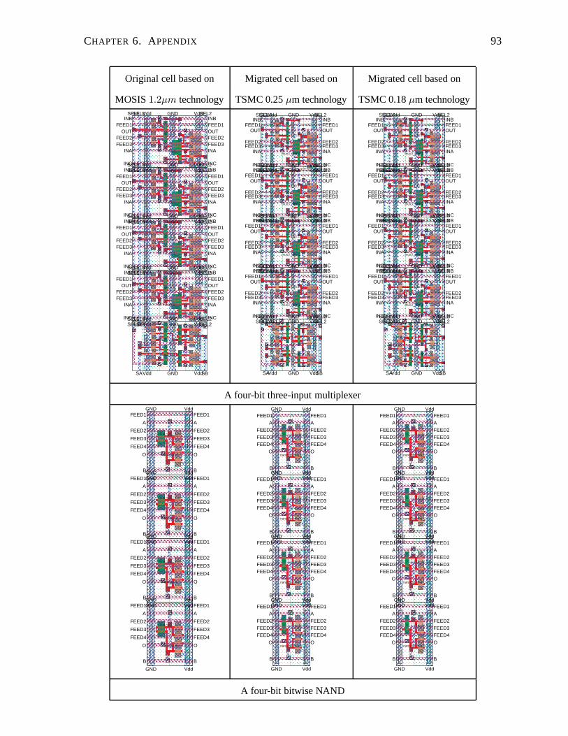
CHAPTER 6. APPENDIX 93
Original cell based on Migrated cell based on Migrated cell based on
MOSIS1.2µm technology TSMC 0.25µm technology TSMC 0.18µm technology
������������������������
��������������������������������
������������������������
��������������������������������
������������������������
��������������������������������
���������������������������
������������������������������������
���������������������
���������������������
���������������������������������������������������������������������������������������������������������������������������������������������������������������������������������������
����������������������
�������������
���������������
����������
���������������
�����
���������������������
�� �
���
��� �
���
��
��
���
�� �
�
��
����������
����
��������
���������
��������������������������
����������
����
��������
�����������
�������������������������������
����������
�������������
����
������������������
����������������
����������
�������������
���� ���
��������������������������
����
������������ ��
������
�������������
���������
���������
��������
�� ������������������������ ���
����������
������ �������
���������
������
������ ����� ���
���������
������ ����� ���
�������
�������� ����� ���
�������
����������
�����
�� ����
�����
������
������������
���
�������������
���������������
�������������
��
��� ��
����
��
����������
��
���������������������������
������ ������
����� �
����� ��� ���������������� �
�
������
����
��������� ��
��������
���� ��
������������
�����������������
���� �����
����� �
����� ��� �������������� ����������������� �
��������� �
�������������������
������������ ���������
���� ��
���� ����� �������
����
������� ����������������
�
��������� �����������
��������������������� �
�������� ��
���� �����
��
������������� ������
��������
�������
�
�� ��
������������
�����������������
�� �� �
� �� ������������
������������
�����
���
�
�� ����������� ��������
��� ���� ��
������ �������
���������
������
������ ����� ���
���������
������ ����� ���
�������
�������� ����� ���
�������
����������
�����
�� ����
�����
������
������������
���
�������������
���������������
�������������
��
��� ��
����
��
���
��
���
��
���
�
���
�
��
���
���
������
�� ������
����������
��
������
���� ��
��
����������
��
����
���� ��
��
����������
��
����
������
����������
��
����
���� �
�
mux3
mux3_3
mux3
mux3_2
mux3
mux3_1
mux3
mux3_0
mux3_cs1
mux3_cs1_0
GNDVdd
Vdd GND Vdd
Vdd
OUTOUT
INC INCSEL2
SEL2
FEED1 FEED1
FEED2FEED3
FEED2FEED3
INA
INB INB
INA
SEL0SEL1
SEL1SEL0
GNDVdd
Vdd GND Vdd
Vdd
OUTOUT
INC INCSEL2
SEL2
FEED1 FEED1
FEED2FEED3
FEED2FEED3
INA
INB INB
INA
SEL0SEL1
SEL1SEL0
GNDVdd
Vdd GND Vdd
Vdd
OUTOUT
INC INCSEL2
SEL2
FEED1 FEED1
FEED2FEED3
FEED2FEED3
INA
INB INB
INA
SEL0SEL1
SEL1SEL0
GNDVdd
Vdd GND Vdd
Vdd
OUTOUT
INC INCSEL2
SEL2
FEED1 FEED1
FEED2FEED3
FEED2FEED3
INA
INB INB
INA
SEL0SEL1
SEL1SEL0
SEL0SEL1 SEL2Vdd VddGND
SA GND VddVdd SB
������������������������������������
������������������������������������
������������������������������������
������������������������������������
������������������������������������
������������������������������������
������������������������������������
������������������������������������
��������������������������������
��������������������������������
���������������������������
���������������������������
���������������������������
���������������������������
������������������������
���
�������������������������
���
�������������������������
�������������
���������������
�������������
���������������
���
����
��
�� �
���
���
�
��
��� �
�
�����
�� ���
����
���
������������������������
�����
��
���������
���
������������������������
�����
��
���������
���
��������������������������
����
��
���������
���
��������������������������
����������
�������
����
�����
����
������
� �������
����������� ��
�����
��� ����
����������
��� ��� ��
��������
��� ��� ��
������
��� ��� ��
������
���
��
���
�� �
���� ����
������������
������������
������������
�������������
���
� ���
���� ��
��������
����� ��
���������������������������
�����������
������� �
�������� �����������������������������������
��������
����� ��
���������������������������
����������
������ �
�������� �����������������������������������
��������
����� ��
��������������������������
����������
������ �
�������� ��������������������������������
�
���������� �
�������������
������������������
����������
������ �
�������� ��������������������������������
�
����������������������
�����������
�� �
��������������������
�����������
����������
�
�� ���������������
����������������������
��� ����
����������
��� ��� ��
��������
��� ��� ��
������
��� ��� ��
������
���
��
���
�� �
���� ����
������������
������������
������������
�������������
���
� ���
���� ��
���
��
���
��
���
��
���
�
��
��
��
��
� ��
�����
��
��
� ��
�����
��
��
� ��
�����
��
��� �
�
�����
��
��
� ���
mux3_mig
mux3_mig_3
mux3_mig
mux3_mig_2
mux3_mig
mux3_mig_1
mux3_mig
mux3_mig_0
mux3_cs1_mig
mux3_cs1_mig_0
SEL1SEL0Vdd GND VddSEL2
SEL1SEL0Vdd GND VddSEL2
INC
INAFEED3FEED2
OUTFEED1INB
INC
INAFEED3FEED2
OUTFEED1
INB
SEL1SEL0Vdd GND VddSEL2
SEL1SEL0Vdd GND VddSEL2
INC
INAFEED3FEED2
OUTFEED1INB
INC
INAFEED3FEED2
OUTFEED1
INB
SEL1SEL0Vdd GND VddSEL2
SEL1SEL0Vdd GND VddSEL2
INC
INAFEED3FEED2
OUTFEED1INB
INC
INAFEED3FEED2
OUTFEED1
INB
SEL1SEL0Vdd GND VddSEL2
SEL1SEL0Vdd GND VddSEL2
INC
INAFEED3FEED2
OUTFEED1INB
INC
INAFEED3FEED2
OUTFEED1
INB
SAVdd GND Vdd
SEL1SEL0Vdd GND Vdd
SB
SEL2
������������������������������������
������������������������������������
������������������������������������
������������������������������������
������������������������������������
������������������������������������
������������������������������������
������������������������������������
��������������������������������
��������������������������������
���������������������������
���������������������������
���������������������������
���������������������������
������������������������
���
�������������������������
���
�������������������������
����������������������������
����������������������������
�������
��
�� ����
����
��
��� ��
�����
�� ���
����
���
������������������������
�����
��
���������
���
������������������������
�����
��
���������
���
��������������������������
����
��
���������
���
��������������������������
����������
�������
����
�����
����
������
� �������
����������� ��
�����
��� ����
����������
��� ��� ��
��������
��� ��� ��
������
��� ��� ��
������
���
��
���
�� �
��
�� ����
������������
������������
������������
�������������
���
� ���
���� ��
��������
����� ��
���������������������������
�����������
������� �
�������� ��������������������������������
���
��������
����� ��
���������������������������
����������
��
���� ��������� ��������������������������������
���
��������
����� ��
��������������������������
����������
��
���� ��������� ��������������������������������
�
���������� ��
������������
������������������
����������
��
���� ��������� ��������������������������������
�
����������������������
�����������
�� �
��������������������
�����������
����������
�
�� ���������������
����������������������
��� ����
����������
��� ��� ��
��������
��� ��� ��
������
��� ��� ��
������
���
��
���
�� �
��
�� ����
������������
������������
������������
�������������
���
� ���
���� ��
���
��
���
��
���
��
���
�
��
��
��
��
� ��
�����
��
��
� ��
�����
��
��
� ��
�����
��
��� �
�
�����
��
��
� ���
mux3_mig
mux3_mig_3
mux3_mig
mux3_mig_2
mux3_mig
mux3_mig_1
mux3_mig
mux3_mig_0
mux3_cs1_mig
mux3_cs1_mig_0
SEL1SEL0Vdd GND VddSEL2
SEL1SEL0Vdd GND VddSEL2
INC
INAFEED3FEED2
OUTFEED1INB
INC
INAFEED3FEED2
OUTFEED1
INB
SEL1SEL0Vdd GND VddSEL2
SEL1SEL0Vdd GND VddSEL2
INC
INAFEED3FEED2
OUTFEED1INB
INC
INAFEED3FEED2
OUTFEED1
INB
SEL1SEL0Vdd GND VddSEL2
SEL1SEL0Vdd GND VddSEL2
INC
INAFEED3FEED2
OUTFEED1INB
INC
INAFEED3FEED2
OUTFEED1
INB
SEL1SEL0Vdd GND VddSEL2
SEL1SEL0Vdd GND VddSEL2
INC
INAFEED3FEED2
OUTFEED1INB
INC
INAFEED3FEED2
OUTFEED1
INB
SAVdd GND Vdd
SEL1SEL0Vdd GND Vdd
SB
SEL2
A four-bit three-input multiplexer
������������������������������������������������������������������������������������������������������������������������������������������������
������������������������������������������������������������������������������������������������������������������������������������������������
������
����
����
����
����
����
����
����
��������
����������������
����
����
��������������
����������
����
������
����������
����
��������
��
����
����
��
��
����
����
����
����
����
����
������
����
����
����
����
����
��������
������
������
������
��
������
��������
�����
������
�������
��������
�
����������
��������
�������
��������
�
����������
�������������
����������
��
����
����
��
��
����
����
����
����
����
����
������
����
����
����
����
����
���������
���������
���������
���������
���������
���������
���������
���������
nand2lp
nand2lp_3
nand2lp
nand2lp_2
nand2lp
nand2lp_1
nand2lp
nand2lp_0
B
O
GND
GND
A
Vdd
B
O
A
FEED1
FEED2
FEED3
FEED4 FEED4
FEED3
FEED2
FEED1Vdd
B
O
GND
GND
A
Vdd
B
O
A
FEED1
FEED2
FEED3
FEED4 FEED4
FEED3
FEED2
FEED1Vdd
B
O
GND
GND
A
Vdd
B
O
A
FEED1
FEED2
FEED3
FEED4 FEED4
FEED3
FEED2
FEED1Vdd
B
O
GND
GND
A
Vdd
B
O
A
FEED1
FEED2
FEED3
FEED4 FEED4
FEED3
FEED2
FEED1Vdd
������������������������������������������������������������������������������������������������������������������������������������������������
������������������������������������������������������������������������������������������������������������
�
���
���
��
��
�
��
��
�
����
��
�����
����
��
�����
��
��
��
��
�����
��
��
��
��
�����
��
���
��
���
�
���
�
���
��
�
��
��
�
��
��
�������������
����
����������������������������
�������������
��������
����������������������������
�������
��������
���������
��������������������
�����������
���������
������������������
��
���
��
���
�
���
�
���
��
�
��
��
�
��
��
��������
��������
��������
��������
��������
��������
��������
��������
nand2lp_mig
nand2lp_mig_3
nand2lp_mig
nand2lp_mig_2
nand2lp_mig
nand2lp_mig_1
nand2lp_mig
nand2lp_mig_0
GND Vdd
GND Vdd
B
O
FEED4FEED3
FEED2
AFEED1
B
O
FEED4FEED3
FEED2
AFEED1
GND Vdd
GND Vdd
B
O
FEED4FEED3
FEED2A
FEED1
B
O
FEED4FEED3
FEED2A
FEED1
GND Vdd
GND Vdd
B
O
FEED4FEED3
FEED2AFEED1
B
O
FEED4FEED3
FEED2A
FEED1
GND Vdd
GND Vdd
B
O
FEED4FEED3
FEED2
A
FEED1
B
O
FEED4FEED3
FEED2
A
FEED1
A four-bit bitwise NAND
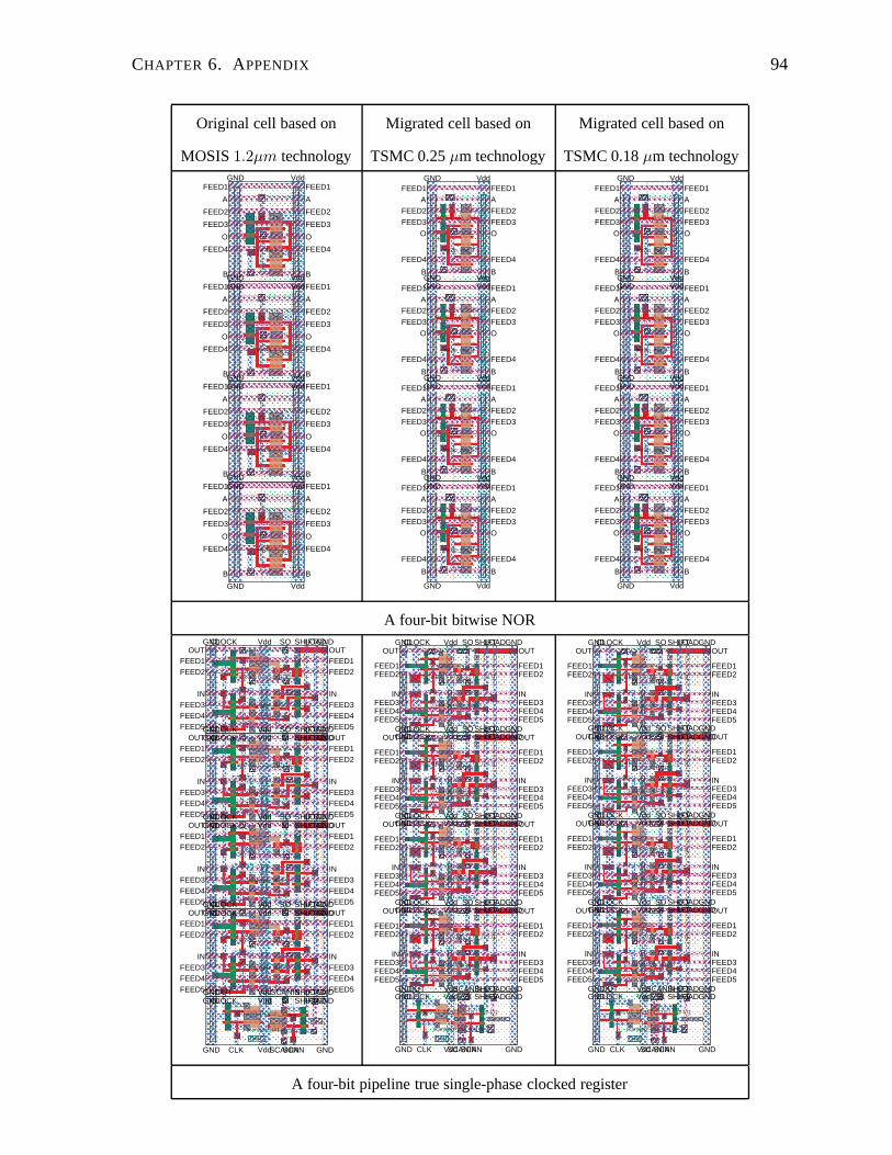
CHAPTER 6. APPENDIX 94
Original cell based on Migrated cell based on Migrated cell based on
MOSIS1.2µm technology TSMC 0.25µm technology TSMC 0.18µm technology
������������������������������������������������������������������������������������������������������������������������������������������������������������������������������������
������������������������������������������������������������������������������������������������������������
������
������
����
����
��
����
����
����
����������
����
��������
������������
����������
����
������������
����������
����
��������������������
����������������
������������
����
����������
����
����������
������
����
����
����
����
��
����
����
��������
����
��������������
���
�������
��
�������
��
��������
����
�������������� �
�
������
����
��
������
����������������������� �
��
������
����
��
������
���������������������� �
��
������
���� �������
���
����������������
������������
����
����������
����
����������
������
����
����
����
����
��
����
����
���������
���������
���������
���������
������������������
������������������
������������������
������������������
nor2lp
nor2lp_3
nor2lp
nor2lp_2
nor2lp
nor2lp_1
nor2lp
nor2lp_0
Vdd
B
O
Vdd
A
O
A
GND
GND
B
FEED1
FEED2
FEED3
FEED4 FEED4
FEED3
FEED2
FEED1
Vdd
B
O
Vdd
A
O
A
GND
GND
B
FEED1
FEED2
FEED3
FEED4 FEED4
FEED3
FEED2
FEED1
Vdd
B
O
Vdd
A
O
A
GND
GND
B
FEED1
FEED2
FEED3
FEED4 FEED4
FEED3
FEED2
FEED1
Vdd
B
O
Vdd
A
O
A
GND
GND
B
FEED1
FEED2
FEED3
FEED4 FEED4
FEED3
FEED2
FEED1
������������������������������������������������������������������������������������������������������������������������������������������������
������������������������������������������������������������������������������������������������������������
��
��
��
��
��
��
��
��
��
��
��
��
��
����������
��
��������
���
��������
��
��
��������
��
��
�����
���
����
���
���
�����
���
�����
��
��
��
��
��
���������������������� �
��
������
��� �������
����
��
��������������������� �
��
�����
�� �
�
������
����
��
����������
����
���������
����
� ���
�����
�� �
����
����
��
����������
����
���������
����
� ���
�����
�� �
����
����
�����
���
����
���
���
�����
���
�����
��
��
��
��
��������
��������
��������
��������
����������������
����������������
����������������
����������������
nor2lp_mig
nor2lp_mig_3
nor2lp_mig
nor2lp_mig_2
nor2lp_mig
nor2lp_mig_1
nor2lp_mig
nor2lp_mig_0
GND Vdd
GND Vdd
B
FEED4
O
FEED3
FEED2
AFEED1
B
FEED4
O
FEED3
FEED2
AFEED1
GND Vdd
GND Vdd
B
FEED4
O
FEED3
FEED2A
FEED1
B
FEED4
O
FEED3
FEED2A
FEED1
GND Vdd
GND Vdd
B
FEED4
O
FEED3
FEED2AFEED1
B
FEED4
O
FEED3
FEED2A
FEED1
GND Vdd
GND Vdd
B
FEED4
O
FEED3
FEED2
A
FEED1
B
FEED4
O
FEED3
FEED2
A
FEED1
������������������������������������������������������������������������������������������������������������������������������������������������
������������������������������������������������������������������������������������������������������������
��
��
��
��
��
��
��
��
��
��
��
��
��
����������
��
��������
���
��������
��
��
��������
��
��
�����
���
����
���
���
�����
���
�����
��
��
��
��
��
���������������������� �
��
������
��� �������
����
��
��������������������� �
��
�����
�� �
�
������
����
��
��������������
�������������
� ���
�����
�� �
��������
��
��������������
�������������
� ���
�����
�� �
��������
�����
���
����
���
���
�����
���
�����
��
��
��
��
��������
��������
��������
��������
����������������
����������������
����������������
����������������
nor2lp_mig
nor2lp_mig_3
nor2lp_mig
nor2lp_mig_2
nor2lp_mig
nor2lp_mig_1
nor2lp_mig
nor2lp_mig_0
GND Vdd
GND Vdd
B
FEED4
O
FEED3
FEED2
AFEED1
B
FEED4
O
FEED3
FEED2
AFEED1
GND Vdd
GND Vdd
B
FEED4
O
FEED3
FEED2A
FEED1
B
FEED4
O
FEED3
FEED2A
FEED1
GND Vdd
GND Vdd
B
FEED4
O
FEED3
FEED2AFEED1
B
FEED4
O
FEED3
FEED2A
FEED1
GND Vdd
GND Vdd
B
FEED4
O
FEED3
FEED2
A
FEED1
B
FEED4
O
FEED3
FEED2
A
FEED1
A four-bit bitwise NOR
����������������������������������������������������������������������������������������������������������������������������������������������������������������
������������������������������
������������������������������������
������������������������������������
��������������������������������
��������������������������������
������������������������������������
������������������������������������
������������������������������������
������������������������������������
���������������
��������������������
���
������
���
����������
�����
����
������
�� ��
����������
����������
����
������
�
������
����
�� ��
���������
����������
���
������
�
����
������
�� ��
��
���������
����������
����
������
�
����
������
� ����
���� �
��� ��� �
�
��
��������
����������������������������
��
������
����� �
����
����
��������
����������������������
��
����
����
���
��
�� �������������������������������
��
����
����
��
���
�� ��
�������������������������������
����
����
��
���
�� ��
������
�������������
�������������
�����������������
�������
�� ��
��
����
�������
����
����
������
������
��
����
������
���������
��
����
����
����
�������
���
����
����
�� ����
����
�
��� ��
������
�
��
��� ��
��
���
����
�
���� ��
��
��
����
�
����
���� �
�
������������ ����� �����������
��� �������
����
� � ������
�����������������
� ����
������������� �
�
����������������
���������� ��
������
����������
�������� ����� ��������
�� �����
������
� �� ���
������
�������������
������
��������
��
����������
����������
����������
���������������� �
�
��������
��
�������
�� ��
��������������
� �� ���
���������������
������� ��
�������� �
������������������
��������
������������
��������������
��
���� �������
�� ��
����������
�� � ���
����������������
�� ��
�������� �
������������������� ������
��
���
����������������� ���
������
���� �����
� � ��������
����
�������
�� ��
��
����
�������
����
����
������
������
��
����
������
���������
��
����
����
����
�������
���
����
����
�� ����
����
�
��� ��
������
�
��
��� ��
��
���
����
�
���� ��
��
��
����
�
����
���� �
�
��
����
����
������
�
��
����
����
������
��
���������
����
������
��
���������
����
������
��
�����
����
���
�
���
�
����
��
����
��
��
���
scantspcr_fb
scantspcr_fb_3
scantspcr_fb
scantspcr_fb_2
scantspcr_fb
scantspcr_fb_1
scantspcr_fb
scantspcr_fb_0
scantspcr_cs1
scantspcr_cs1_0
Vdd
Vdd
GND
OUTFEED1FEED2
GND
CLOCK
CLOCK
IN
FEED5FEED4FEED3
SI
SO
GND
GND
IN
OUTFEED1
FEED5FEED4FEED3
SHIFTLOAD
SHIFTLOAD
FEED2
Vdd
Vdd
GND
OUTFEED1FEED2
GND
CLOCK
CLOCK
IN
FEED5FEED4FEED3
SI
SO
GND
GND
IN
OUTFEED1
FEED5FEED4FEED3
SHIFTLOAD
SHIFTLOAD
FEED2
Vdd
Vdd
GND
OUTFEED1FEED2
GND
CLOCK
CLOCK
IN
FEED5FEED4FEED3
SI
SO
GND
GND
IN
OUTFEED1
FEED5FEED4FEED3
SHIFTLOAD
SHIFTLOAD
FEED2
Vdd
Vdd
GND
OUTFEED1FEED2
GND
CLOCK
CLOCK
IN
FEED5FEED4FEED3
SI
SO
GND
GND
IN
OUTFEED1
FEED5FEED4FEED3
SHIFTLOAD
SHIFTLOAD
FEED2
GNDOUT Vdd
GND VddCLK
SHIFTSCANIN
SCANINSCAN GND
GNDLOAD������������������������������������������������������������������������������������������������
�������������������������
������������������������������������
������������������������������������������������������
��������������������������������
������������������������������������������������
������������������������������������
������������������������������������������������������
������������������������������������
������������������������������������������������������
���������������
�������������������������
���
���������
��������
�����
����
������
�� ��
���
���������� ��
�������
����
�������
��������
� ����
���������
��������
��������
����
������
���
���
�������
��������
��
�������
����
������
�� ��
��
��
��
� ��� �
�
��������������������������
������� ��
����������������������������
��
������
� ��
���
���������������������
�����
���� �
���
��������������������������
�����
���� �
���
������������������������������������
�����
� ��
��
��
�����
���
��
����
������
���
���
�����
����
�
����������
����
��
�� ����
����
�
��� �
������
�
��
��� �
�
��
����
��
��� �
�
��
�����
�� �
��
����������
�����������������������������
�������������
������
���� ������
��������������������
� ��
������������
� ��
��������������
�����������
�������������
��������������������������������������
�������
������ ���
���������������������
��
��
��������
��
�������������������� ���������������
����������������
�
��������
��
����������������
����������������
�������� ���
������������������
�� ��������� �
������������������������ ������
���������
����������
�������������������������������������
������
������ ���
������������������
�� ��������� �
�
������������������ ��
������
���������
������������
������������ ������
��������
��
��
���
�����
� ��
��
��
�����
���
��
����
������
���
���
�����
����
�
����������
����
��
�� ����
����
�
��� �
������
�
��
��� �
�
��
����
��
��� �
�
��
�����
�� �
��
��
�����
����
������
��
�����������
����
������
��
�����������
����
������
�
��
��������
����
������
�
�����
���
���
�
���
��
���
�
���
�
��
��
scantspcr_fb_mig
scantspcr_fb_mig_3
scantspcr_fb_mig
scantspcr_fb_mig_2
scantspcr_fb_mig
scantspcr_fb_mig_1
scantspcr_fb_mig
scantspcr_fb_mig_0
scantspcr_cs1_mig
scantspcr_cs1_mig_0
GNDCLOCK Vdd SI SHIFTLOADGND
GNDCLOCK Vdd SOSHIFTLOADGND
FEED5FEED4FEED3IN
FEED2FEED1
OUT
FEED5FEED4FEED3
IN
FEED2FEED1
OUT
GNDCLOCK Vdd SI SHIFTLOADGND
GNDCLOCK Vdd SOSHIFTLOADGND
FEED5FEED4FEED3IN
FEED2FEED1
OUT
FEED5FEED4FEED3
IN
FEED2FEED1
OUT
GNDCLOCK Vdd SI SHIFTLOADGND
GNDCLOCK Vdd SOSHIFTLOADGND
FEED5FEED4FEED3IN
FEED2FEED1
OUT
FEED5FEED4FEED3
IN
FEED2FEED1
OUT
GNDCLOCK Vdd SI SHIFTLOADGND
GNDCLOCK Vdd SOSHIFTLOADGND
FEED5FEED4FEED3IN
FEED2FEED1
OUT
FEED5FEED4FEED3
IN
FEED2FEED1
OUT
GND CLK VddSCANINSCAN GND
GNDOUT VddSCANINSHIFTLOADGND
���������������������������
������������������������������������������������������������������������
�������������������������
������������������������������������
������������������������������������������������������
��������������������������������
������������������������������������������������
������������������������������������
������������������������������������������������������
������������������������������������
������������������������������������������������������
���������������
�������������������������
���
������
���
��������
��������
������
�� ��
�����������
����
����
���
������
�
��������
� ����
��������
��
��������
��������
����
������
���
���
�������
������
��
�������
����
������
�� ��
��
��
��
� ��� �
�
��������������������������
��
���� �
���������������������
��������
��
������
� ��
���
�����������������������
�����
���� �
���
��������������������������
�����
���� �
���
������������������������������������
�����
�� ��
��
��
�����
���
��
��������
���
���
�����
����
�
����������
����
��
��� ��
��
����
�
��� �
������
�
���� �
�
��
����
��
��� �
�
��
�����
�� �
��
����������
�������������������
����������
�������������
������
���� ������
����
���������
������
��������� �
�
������������� ��
��������������
�����������
�������������
����������������������
�������
���������
�������
������ ���
��������������������
�� �������
�� �
����������������
���� ��������
�������
���������������������
���������������
����������������������
������ ���
������������������
�� �������
�� �
������������������������ ������
���������
����������
����������������
���������������������
������
������ ���
������������������
�� �
�
�������� ��
������������������ ��
������
���������
������������������������ ����
����������
��
��
���
�����
�� ��
��
��
�����
���
��
��������
���
���
�����
����
�
����������
����
��
��� ��
��
����
�
��� �
������
�
���� �
�
��
����
��
��� �
�
��
�����
�� �
��
��
�����
����
������
��
�����������
����
������
��
�����������
����
������
�
��
��������
����
����
�
�����
���
���
�
���
��
���
�
���
�
��
��
scantspcr_fb_mig
scantspcr_fb_mig_3
scantspcr_fb_mig
scantspcr_fb_mig_2
scantspcr_fb_mig
scantspcr_fb_mig_1
scantspcr_fb_mig
scantspcr_fb_mig_0
scantspcr_cs1_mig
scantspcr_cs1_mig_0
GNDCLOCK Vdd SI SHIFTLOADGND
GNDCLOCK Vdd SO SHIFTLOADGND
FEED5FEED4FEED3IN
FEED2FEED1
OUT
FEED5FEED4FEED3
IN
FEED2FEED1
OUT
GNDCLOCK Vdd SI SHIFTLOADGND
GNDCLOCK Vdd SO SHIFTLOADGND
FEED5FEED4FEED3IN
FEED2FEED1
OUT
FEED5FEED4FEED3
IN
FEED2FEED1
OUT
GNDCLOCK Vdd SI SHIFTLOADGND
GNDCLOCK Vdd SO SHIFTLOADGND
FEED5FEED4FEED3IN
FEED2FEED1
OUT
FEED5FEED4FEED3
IN
FEED2FEED1
OUT
GNDCLOCK Vdd SI SHIFTLOADGND
GNDCLOCK Vdd SO SHIFTLOADGND
FEED5FEED4FEED3IN
FEED2FEED1
OUT
FEED5FEED4FEED3
IN
FEED2FEED1
OUT
GND CLK VddSCANINSCAN GND
GNDOUT VddSCANINSHIFTLOADGND
A four-bit pipeline true single-phase clocked register

CHAPTER 6. APPENDIX 95
Original cell based on Migrated cell based on Migrated cell based on
MOSIS1.2µm technology TSMC 0.25µm technology TSMC 0.18µm technology
������������
������������
������������
������������
������������
������������
���������������
���������������
�� ��
��������
������������
��������
��������
������������
��������
��������
������������
��������
����������
���������������
����������
���
����������
���������
������
����� ������ ��
������������ �������� ���� ����
����������
���������
������
����� ������ ��
������������ �������� ���� ����
����������
��������������
������ ����� ������������� ��������� ���� ����
����������
��������������
������ ����� ������������ ��������� ���� ��������
���������������� ��
���
�����
� ������� ��
����������
� �� ���� ���
� ��� � ��������������������������������� ��
���
�����
� ������� ��
����������
� �� ���� ���
� ��� � �������������������������������� ��
���
�����
� ������ �������
����
� �� ���� ����
� ��� � �������������������������������� ��
��� �
�����
� ������ �������
����
� �� ���� ����
� ��� � ������������������� ����
���� ����
�� ����� �
� �� �����
����� ����
�� ����� �
� �� �����
���� ��
���
� ����� �� �� �������� ��
�� ��
� ����� �� �� ����
� �
���� �������
� ��� ������
�� ��� � �������� ������� �
� ��� ������
�� ��� � ������
������� �
��� ������� ��� � ��
����
������� � ��
��� ������� ��� � ����
�������������������
��������
���������� �������������������������
����������
�������������������������
����������������� ���������� ���
�������������������� ���������������
������������� ������������������������ �
�������������
���������� ��������������������������
����������
����������������������
����������������������� ���������� ���
�������������������� ����������������������������� �
��������������������� �
��������
���������� ��������������������������
���������� �
��������������������
������������������������ ���������
�� ��
��
����������������� ������������������������� �
��������������������� ����������������� ��������������������������
���������� �
����������������������������������������������
������ ���������
�� �
�������������������� �������������������������� �
������ ����������� �
���� ����
�� ����� �
� �� �����
����� ����
�� ����� �
� �� �����
���� ��
���
� ����� �� �� �������� ��
�� ��
� ����� �� �� ����
� �
���� �������
� ��� ������
�� ��� � �������� ������� �
� ��� ������
�� ��� � ������
������� �
��� ������� ��� � ��
����
������� � ��
��� ������� ��� � ����
����
����
��� �
���
����
����
��� �
���
���
����
��� �
��
���
����
��� �
��
�
��
��� �
��
� ����
��� �
��
� ���
��� �
�� ���
��� �
�� ��� �
sub
sub_3
sub
sub_2
sub
sub_1
sub
sub_0
sub_cs_selsub_cs_sel_0
Vdd VddCOUT
CIN
GNDCOUTINV
CININVGND GND GNDVddVdd
GNDB
FEED1FEED2FEED3
AFEED4
SUM
BFEED1FEED2FEED3AFEED4SUM
GND
Vdd VddCOUT
CIN
GNDCOUTINV
CININVGND GND GNDVddVdd
GNDB
FEED1FEED2FEED3
AFEED4
SUM
BFEED1FEED2FEED3AFEED4SUM
GND
Vdd VddCOUT
CIN
GNDCOUTINV
CININVGND GND GNDVddVdd
GNDB
FEED1FEED2FEED3
AFEED4
SUM
BFEED1FEED2FEED3AFEED4SUM
GND
Vdd VddCOUT
CIN
GNDCOUTINV
CININVGND GND GNDVddVdd
GNDB
FEED1FEED2FEED3
AFEED4
SUM
BFEED1FEED2FEED3AFEED4SUM
GND
GND GND GNDVddVdd COUTINV COUT
GNDCARRYINVdd Vdd GNDGND
������������
��� ������������
������������
��� ������������
������������
��� ������������
���������
������
������������
��� ��
����
������������
��� ����
����
������������
��� ����
����
������������
��� ����
����
���������
������
����
��
������ ���������������
������������� ���� ������������� ����
�� ������ �
��
������ ���������������
�������������� ������ �
������������� ��
����
�� ������ ��
������������������
�������������� ���� �
�������
�������� ������ ����� ��
������������������
�������������� ���� �������
��������� ���
���� ����� ��������
�������������� ���������
�������������� ������������
���������������
������������� ��������
������������
�������� ������������ �
�������������
����������� ���������
������������
����
������������ ������������������������ ����������
�����������
����
��������
����� ��������������� ����
��� ����
�����
�� ����
���
��� ����
����� �
������
��� ����
����� �
��� ����
��� ���� �
����� �
��� ���� �
�� ��������� ���
��
����� ��� � ��� ��������� �� �����
� ��� � ��������
�� ���
� ������
� ��� � ��������
�� �� ��
� ������ ��� � �
���
���������������������
�����������
�������������
�������������������������������������������������������
������������������������������������������������
���������������������
�������������������� �
�����������
������������������������������������������
��������������������������������������������������������
��
��������������������������
���������������������������������� ����������������������������������������������
���������������������������������������������������������
������������������������������������������������
��������������������� �����������������������������������������������
������������������������������������������
��������������
����������������������������������������������������
����� ���������� �
��� ����
�����
�� ����
���
��� ����
����� �
������
��� ����
����� �
��� ����
��� ���� �
����� �
��� ���� �
�� ��������� ���
��
����� ��� � ��� ��������� �� �����
� ��� � ��������
�� ���
� ������
� ��� � ��������
�� �� ��
� ������ ��� � �
���
����
��� �
���
����
���� �
���
���
��
��� �
��
���
��
��� �
��
�
��
�� ���
� ����
��
�� ��
��
� ����
��� ��
�� ����
��� ��
�� ���� ��
sub_mig
sub_mig_3
sub_mig
sub_mig_2
sub_mig
sub_mig_1
sub_mig
sub_mig_0
sub_cs_sel_migsub_cs_sel_mig_0
GND Vdd CININVGND Vdd CIN GND
GND VddCOUTINVGND VddCOUT GND
SUMFEED4
AFEED3
FEED2FEED1B
SUMFEED4
AFEED3
FEED2FEED1
B
GND Vdd CININVGND Vdd CIN GND
GND VddCOUTINVGND VddCOUT GND
SUMFEED4
AFEED3
FEED2FEED1B
SUMFEED4
AFEED3
FEED2FEED1
B
GND Vdd CININVGND Vdd CIN GND
GND VddCOUTINVGND VddCOUT GND
SUMFEED4
AFEED3
FEED2FEED1B
SUMFEED4
AFEED3
FEED2FEED1
B
GND Vdd CININVGND Vdd CIN GND
GND VddCOUTINVGND VddCOUT GND
SUMFEED4
AFEED3
FEED2FEED1B
SUMFEED4
AFEED3
FEED2FEED1
B
GND VddCARRYIN GND Vdd GND
GND Vdd GND VddCOUT GNDCOUTINV
������������
��� ������������
������������
��� ������������
������������
��� ������������
���������
������
������������
��� ��
����
������������
��� ����
����
������������
��� ����
����
������������
��� ����
����
���������
������
����
��
������ ��
�������������
������������� ���� ������������� ����
�� ������ �
��
������ ��
�������������
���
����������� ������ �
������������� ������
�� ������ ��
�����
����������������
����������� ���� �
��������������� ������ ����� ��
�����
����������������
����������� ���� ���������������� ������� ����� ��������
�������������� �����������������
������ ������������
���������������
������������� ��������������������
�������� ������������ �
�������������
����������� �������������
������������
������������ ������������������������ ���������������������
����
��������
����� ��������������� ����
��� ����
�����
�� ����
���
��� ����
����� �
������
��� ����
����� �
��� ����
��� ���� �
����� �
��� ���� �
�� �������
�� ���
��
����� ��� � ��� �������
�� �� �����
� ��� � ���
������� ��
�� ������
� ��� � ���
������� �� �
�� ������ ��� � ����
���������������������
������������������������
��
����������������
�������������������������������������
������������������������������������������������
���������������������
�������������������� �
�����������
�������������������
�����������������
������������������������
��������������������������������������
��
��������������������������
���������������������������������� �������������������������
������������������
�������������������������
�����������������������������������
������������������������������������������������
��������������������� �������������������������
������������������
����������������������������������������������
�������������������������������������������������
�����������������
����� ���������� �
��� ����
�����
�� ����
���
��� ����
����� �
������
��� ����
����� �
��� ����
��� ���� �
����� �
��� ���� �
�� �������
�� ���
��
����� ��� � ��� �������
�� �� �����
� ��� � ���
������� ��
�� ������
� ��� � ���
������� �� �
�� ������ ��� � ����
����
��� �
���
����
���� �
���
���
��
��� �
��
���
��
��� �
��
�
��
�� ���
� ��
����
�� ��
��
� ����
��� ��
�� ����
��� ��
�� ���� ��
sub_mig
sub_mig_3
sub_mig
sub_mig_2
sub_mig
sub_mig_1
sub_mig
sub_mig_0
sub_cs_sel_migsub_cs_sel_mig_0
GND Vdd CININVGND Vdd CIN GND
GND VddCOUTINVGND VddCOUT GND
SUMFEED4
AFEED3
FEED2FEED1B
SUMFEED4
AFEED3
FEED2FEED1
B
GND Vdd CININVGND Vdd CIN GND
GND VddCOUTINVGND VddCOUT GND
SUMFEED4
AFEED3
FEED2FEED1B
SUMFEED4
AFEED3
FEED2FEED1
B
GND Vdd CININVGND Vdd CIN GND
GND VddCOUTINVGND VddCOUT GND
SUMFEED4
AFEED3
FEED2FEED1B
SUMFEED4
AFEED3
FEED2FEED1
B
GND Vdd CININVGND Vdd CIN GND
GND VddCOUTINVGND VddCOUT GND
SUMFEED4
AFEED3
FEED2FEED1B
SUMFEED4
AFEED3
FEED2FEED1
B
GND VddCARRYIN GND Vdd GND
GND Vdd GND VddCOUT GNDCOUTINV
A four-bit substractor
������������������������������������������������������������������������������������������������������������������������������������������������
������������������������������������������������������������������������������������������������������������
��������
���������
������������������
�����������������
���������������
��������
����
������
���������
��������������
���������������������
����������������������
���������������������
������������������
���������
������������
������������
��������
������
����
����������
������
��
������
������
��������
����
������
������
��
����
����������������������������
����������
��
����
����
��
����������
���������
��������������
������
����
����
����
������������������
��
�����������
���������������
����
�����
����
����
��
��������
����
�����������������
����������
�����������
������
�������
��
��������
������������
������������
��������
������
����
����������
������
��
������
������
��������
����
������
������
��
������
������
����
������
������
������
������
������
������������
��
����
��
����
��
����
���
����
���
tribufs
tribufs_3
tribufs
tribufs_2
tribufs
tribufs_1
tribufs
tribufs_0
tribufs_cs1
tribufs_cs1_0
Vdd
Vdd GND
GND
FEED3 FEED3FEED2 FEED2FEED1 FEED1
IN IN
FEED4 FEED4FEED5 FEED5
OUTOUT
ENBAR
ENBAR ENAB
ENABVdd
Vdd GND
GND
FEED3 FEED3FEED2 FEED2FEED1 FEED1
IN IN
FEED4 FEED4FEED5 FEED5
OUTOUT
ENBAR
ENBAR ENAB
ENABVdd
Vdd GND
GND
FEED3 FEED3FEED2 FEED2FEED1 FEED1
IN IN
FEED4 FEED4FEED5 FEED5
OUTOUT
ENBAR
ENBAR ENAB
ENABVdd
Vdd GND
GND
FEED3 FEED3FEED2 FEED2FEED1 FEED1
IN IN
FEED4 FEED4FEED5 FEED5
OUTOUT
ENBAR
ENBAR ENAB
ENABGNDVddENBAR ENAB
Vdd GNDEN������������������������������������������������������������������������������������������������������������
������������������������������������������������������������������������������������������������������������
�������
���������
��������������
��������������
���������������
��
��
������
�����������
��������������
�������������������
������������������������
���������
����������������
����������
������������������
������������
����
������������
������������
����������
��������
�����
��
������
�������
�����
����
���
����������������������������������
���
���
����������
������������
��
�����������������
������
���
��������������������
������������������
���
���
���������������������������������
���
�������
����������������������������
������������
����
������������
������������
����������
��������
�����
��
������
�������
�����
����
���
��
��
���
���
��
��
���
�����
��
��
��
����
��
��
�
����
��
tribufs_mig
tribufs_mig_3
tribufs_mig
tribufs_mig_2
tribufs_mig
tribufs_mig_1
tribufs_mig
tribufs_mig_0
tribufs_cs1_mig
tribufs_cs1_mig_0
ENBARVdd GNDENAB
ENBARVdd GNDENAB
OUTFEED5FEED4FEED3FEED2FEED1IN
OUTFEED5FEED4FEED3FEED2FEED1
IN
ENBARVdd GNDENAB
ENBARVdd GNDENAB
OUTFEED5FEED4FEED3FEED2FEED1IN
OUTFEED5FEED4FEED3FEED2FEED1
IN
ENBARVdd GNDENAB
ENBARVdd GNDENAB
OUTFEED5FEED4FEED3FEED2FEED1IN
OUTFEED5FEED4FEED3FEED2FEED1
IN
ENBARVdd GNDENAB
ENBARVdd GNDENAB
OUTFEED5FEED4FEED3FEED2FEED1IN
OUTFEED5FEED4FEED3FEED2FEED1
IN
Vdd EN GND
ENBARVdd GNDENAB
������������������������������������������������������������������������������������������������������������
������������������������������������������������������������������������������������������������������������
�������
���������
��������������
��������������
���������������
��
��
������
�����������
��������������
�������������������
������������������������
���������
����������������
����������
������������������
������������
����
������������
������������
����������
��������
�����
��
������
�������
�����
����
���
�������������������������
���������
���
���
����
������
��������
������
������������
�����
����
��
���
������������������
��
������������������
���
���
���������������������������
������
���
�������
��������������
��������������
������������
����
������������
������������
����������
��������
�����
��
������
�������
�����
����
���
��
��
���
���
��
��
���
�����
��
��
��
����
��
��
�
����
��
tribufs_mig
tribufs_mig_3
tribufs_mig
tribufs_mig_2
tribufs_mig
tribufs_mig_1
tribufs_mig
tribufs_mig_0
tribufs_cs1_mig
tribufs_cs1_mig_0
ENBARVdd GNDENAB
ENBARVdd GNDENAB
OUTFEED5FEED4FEED3FEED2FEED1IN
OUTFEED5FEED4FEED3FEED2FEED1
IN
ENBARVdd GNDENAB
ENBARVdd GNDENAB
OUTFEED5FEED4FEED3FEED2FEED1IN
OUTFEED5FEED4FEED3FEED2FEED1
IN
ENBARVdd GNDENAB
ENBARVdd GNDENAB
OUTFEED5FEED4FEED3FEED2FEED1IN
OUTFEED5FEED4FEED3FEED2FEED1
IN
ENBARVdd GNDENAB
ENBARVdd GNDENAB
OUTFEED5FEED4FEED3FEED2FEED1IN
OUTFEED5FEED4FEED3FEED2FEED1
IN
Vdd EN GND
ENBARVdd GNDENAB
A four-bit tri-state buffer
Bibliography
[1] A.E.Dunlop. Slim-the translation of symbolic layouts into mask data. InProceeding of
the 20st Design Automation Conference, pages 595–602, 1980.
[2] Michael A.Riepe and Karem A.Sakallah. The edge-based design rule model revisited.
ACM transactions on design automation of electronic system, 3:463–486, July 1998.
[3] Tom Burd. Very low power cell library. Technical report, University of California, Berke-
ley, 1995.
[4] Chung-Kuan Cheng, Xiaotie Deng, Yuh-Zen Liao, and So-Zen Yao. Symbolic layout
compaction under conditional design rules.IEEE Transactions on Computer-Aided De-
sign of Integrated Circuits and Systems, 2:476–486, April 1992.
[5] Y. E. Cho, A. J. Korenjak, and D. E. Stockton. FLOSS: An approach to automated layout
for high-volume designs. InProceeding of the 14st Design Automation Conference, pages
138 – 141, 1977.
[6] Y.Eric Cho. A subjective review of compaction. In22nd Design Automation Conference,
pages 396–404, 1985.
[7] Dan Clein.CMOS IC layout concepts, methodologies, and tools. Newnes, 1999.
[8] Ralph C.Mcgarity and Daniel P.Siewiorek. Experiments with the slim c i r c u i t com-
pactor. InProceeding of the 20st Design Automation Conference, pages 740–746, 1983.
96
BIBLIOGRAPHY 97
[9] David G.Boyer. Symbolic layout compaction review. In25th ACM/IEEE Design Automa-
tion Conference, pages 383–389, 1988.
[10] Fook-Luen Heng, Zhan Chen, and Gustavo E.Tellez. A VLSI artwork legalization tech-
nique based on a new criterion of minimum layout perturbation. In1997 International
Symposium on Physical Design, pages 116–121, 1997.
[11] J.L.Burns and A.R.Newton. Efficient constraint generation for hierachical compaction.
In Proc. of the IEEE international conference on computer design, pages 197–200, 1986.
[12] Christopher Kingsley. A hiererachical, error-tolerant compactor. In21st Design Automa-
tion Conference, pages 126–132, 1984.
[13] Chi-Yuan Lo and Ravi Varadarajan. Ano(n1.5logn) 1-d compaction algorithm. InPro-
ceeding of the 27th Design Automation Conference, pages 382–387, 1990.
[14] Juan Carlos Lopez, Roman Hermida, and Walter Geisselhardt.Advanced techniques for
embedded systems design and test. Kluwer academic publishers, 1998.
[15] David Marple. A hierarchy preserving hierarchical compactor. In27th ACM/IEEE Design
Automation Conference, pages 375–381, 1990.
[16] C. Mead and L. Conway.Introduction to VLSI Systems. Addison-Wesley, 1980.
[17] M.Schiag, Y.Z.Liao, and C.K.Wong. An algorithm for optimal two-dimentional com-
paction of VLSI layouts.Proceedings of ICCAD, pages 88–89, 1983.
[18] M.Y.Hsueh and D.O.Pederson. Computer-aided layout of lsi circuit building-blocks.
Technical report, University of California, Berkeley, 1979.
[19] John K. Ousterhout. Corner stitching: a data-structuring technique for vlsi layout tools.
IEEE transactions on computer-aided design, 1:87–100, January 1984.
BIBLIOGRAPHY 98
[20] P.T.Chapman and Jr K.Clark. The scan line approach to design rules checking: compu-
tational experiences. InProceeding of the 21st Design Automation Conference, pages
235–241, 1984.
[21] Rochit Rajsuman.System-on-a-chip: design and test. Artech House, 2000.
[22] Walter Scott and John Ousterhout. Magic maintainer’s manual #2: The technology file.
Technical report, Lawrence Livermore National Laboratory and University of California,
Berkeley.
[23] Gerard Sierksma.Linear and integer programming : theory and practice. Marcel Dekker,
2002.
[24] George S.Taylor and John K.Ousterhout. Magic’s incremental design rule checker. In
Proceeding of the 21st Design Automation Conference, pages 160–165.
[25] Neil Weste. Virtual grid symbolic layout. In18th Design automation conference, pages
225–233, 1981.
[26] Wayne Wolf, Robert Mathews, John Newkirk, and Robert Dutton. Two-dimentional com-
paction strategies.Proceedings of ICCAD, pages 90–91, 1983.
[27] Jianwen Zhu. Symbolic pointer analysis. InProceedings of the 2002 IEEE/ACM inter-
national conference on Computer-aided design, pages 150– 157, 2002.