wf121 wi-fi module - silicon labs · 2017-02-15 · silicon labs page 10 of 45 . pad number...
TRANSCRIPT
WF121 Wi-Fi MODULE DATA SHEET Tuesday, 14 February 2017 Version 2.0

Silicon Labs
VERSION HISTORY
Version Comment
1.0 First version
1.1 FCC and IC information added
1.2 WF121-N layout guide
1.3 Added power consumption measurements, regulatory info and some corrections
1.4 Added unassociated idle consumption and a chapter about power saving modes
1.4.1 Added CE information
1.4.2 Removed details from the regulatory info
1.4.3 Corrected typos in the pad function tables
1.4.4 Reduced the list of supported coexistence schemes
1.4.5 Added links to Microchip reference guide, some notes on the coexistence
1.4.6 Added inversion notices to RTS/CTS for unambiguity
1.4.7 Added notes on the USB data pins GPIO use being input only to pin function table
1.4.8 Added note on the engineering sample order codes
1.4.9 Additions to power supply description, rewrote power consumption section
1.4.10 Removed references to parallel port and C-libraries
1.4.11 Added recommendations for unconnected GPIO pins
1.4.12 Added notes on Ethernet PHY, various small edits
1.5 Design guidelines, supply voltage limitations
1.5.1 Fixed typos & support/sales contact information
1.5.2 CE info updated
1.5.3 Added possibility for different crystal frequencies

Silicon Labs
1.5.4 Added USB example schematic
1.5.5 Corrections to Firmware section
1.5.6 Noted UART channel limitations, SPI BGAPI limitations
1.5.7 Correction to Reset chapter
1.5.8 Maximum SPI data rate updated
1.5.9 Added notes on Ethernet and 32kHz clock sections
1.5.10 Added a note on UART host bus flow control and clarified SPI host bus notify signal description
1.5.11 Corrected pinout drawing, TX power table
2.0.0 Removed mentions of UART4,5 and Coexistence, updates to current consumption figures, updated latest CE standard versions. Changed contact information and URLs from Bluegiga to Silicon Labs

Silicon Labs
TABLE OF CONTENTS 1 Design guidelines ..........................................................................................................................................7
2 Ordering Information......................................................................................................................................8
3 Pinout and Terminal Descriptions .................................................................................................................9
4 Packaging ................................................................................................................................................... 12 5 Power control .............................................................................................................................................. 15
5.1 Power supply requirements ............................................................................................................... 15
5.2 Power saving functionality ................................................................................................................. 15
5.3 Reset .................................................................................................................................................. 16
6 Interfaces .................................................................................................................................................... 17
6.1 General Purpose I/O pins .................................................................................................................. 17 6.2 Serial ports ......................................................................................................................................... 17
6.3 I2C/SPI ............................................................................................................................................... 18
6.4 USB .................................................................................................................................................... 18
6.5 Ethernet ............................................................................................................................................. 19
6.6 Analog inputs ..................................................................................................................................... 20 6.7 Microcontroller programming interface .............................................................................................. 20
6.8 RF Debug Interface ........................................................................................................................... 21
6.9 CPU Clock ......................................................................................................................................... 21
6.10 32.768 kHz External Reference Clock ............................................................................................... 22
7 Block diagram ............................................................................................................................................. 23
8 Example schematics................................................................................................................................... 24 9 802.11 Radio .............................................................................................................................................. 25
9.1 Wi-Fi Receiver ................................................................................................................................... 25
9.2 Wi-Fi Transmitter ............................................................................................................................... 25
9.3 Regulatory domains ........................................................................................................................... 25
10 Firmware ................................................................................................................................................ 26
11 Host interfaces ....................................................................................................................................... 27 11.1 UART ................................................................................................................................................. 27
11.2 USB .................................................................................................................................................... 27
11.3 SPI ..................................................................................................................................................... 27
12 Electrical characteristics ........................................................................................................................ 28
12.1 Absolute maximum ratings ................................................................................................................ 28 12.2 Recommended operating conditions ................................................................................................. 28
12.3 Input/output terminal characteristics .................................................................................................. 29
12.4 Digital ................................................................................................................................................. 29
12.5 Reset .................................................................................................................................................. 29
12.6 Power consumption ........................................................................................................................... 30

Silicon Labs
13 RF Characteristics ................................................................................................................................. 32
14 Physical dimensions .............................................................................................................................. 34
15 Layout guidelines ................................................................................................................................... 35
15.1 WF121-E ............................................................................................................................................ 35 15.2 WF121-N............................................................................................................................................ 35
15.3 WF121-A ............................................................................................................................................ 36
15.4 Thermal considerations ..................................................................................................................... 37
15.5 EMC considerations ........................................................................................................................... 37
16 Soldering recommendations .................................................................................................................. 39
17 Certifications .......................................................................................................................................... 40 17.1 CE ...................................................................................................................................................... 40
17.2 FCC and IC ........................................................................................................................................ 40
17.2.1 FCC et IC ................................................................................................................................... 42
18 Qualified Antenna Types for WF121-E .................................................................................................. 45

Silicon Labs
DESCRIPTION
WF121 is a self-contained Wi-Fi module providing a fully integrated 2.4GHz 802.11 b/g/n radio and a 32-bit microcontroller (MCU) platform, making it an ideal product for embedded applications requiring simple, low-cost and low-power wireless TCP/IP connectivity. WF121 also provides flexible interfaces for connecting to various peripherals.
WF121 allows end user applications to be embedded onto the on-board 32-bit microcontroller using a simple BGScriptTM scripting. This cuts out the need of an external MCU and allows the development of smaller and lower-cost products. However WF121 can also be used in modem-like mode in applications where the external MCU is needed.
With an integrated 802.11 radio, antenna, single power supply, and regulatory certifications, WF121 provides a low-risk and fast time-to-market for applications requiring Internet connectivity. This combined with Bluegiga’s excellent customer service will turn your Internet-of-Things applications into reality.
APPLICATIONS:
• PoS terminals
• RFID and laser scanners
• Wi-Fi internet radios and audio streaming products
• Wireless cameras
• Video streaming
• Portable navigation devices
• Portable handheld devices
• Wi-Fi medical sensors
• Wireless picture frames
KEY FEATURES:
2.4GHz band IEEE 802.11 b/g/n radio
Excellent radio performance:
TX power: +16 dBm
RX sensitivity: -97 dBm
Host interfaces:
20Mbps UART
SPI
USB device
Peripheral interfaces:
GPIO, ADC and timers
I2C, SPI and UART
Ethernet
Embedded TCP/IP and 802.11 MAC
stacks:
IP, TCP, UDP, DHCP and DNS
protocols
BGAPI host protocol for modem
like usage
BGScriptTM scripting language
32-bit embedded microcontroller
80MHz, 128kB RAM and 512kB
Flash
MIPS architecture
Temperature range: -40oC to +85oC
Fully CE, FCC, IC, South Korea and
Japan qualified
PHYSICAL OUTLOOK:
WF121-A

Silicon Labs
Page 7 of 45
1 Design guidelines

Silicon Labs
Page 8 of 45
2 Ordering Information
Product code Description
WF121-A WF121 module with integrated antenna, 500 units per Reel.
WF121-E WF121 module with U.FL connector, 500 units per Reel.
WF121-N
WF121 module with RF pin.
Non-standard product, so minimum order quantity applies.
Please contact sales through: www.silabs.com
DKWF121 WF121 development kit
Note: Modules with order code ending in –v1 are sold as engineering samples, while those with code –v2 are production units. The difference between the two is in the microcontroller version used, the –v2 version fixes a hardware bug that in some circumstances may cause rare bit errors. The modules differ in outlook in that the –v1 only has the Bluegiga logo and text “WF121” while –v2 versions also have FCC/IC ID codes and CE logo.

Silicon Labs
Page 9 of 45
3 Pinout and Terminal Descriptions
Figure 1: WF121 pinout

Silicon Labs
Page 10 of 45
Pad number Function Description
9 VDD_3.3V Module power supply
8 VDD_PA RF power amplifier power supply
1, 16, 26, 45, 48, 50 GND Ground, connected together internally but should all be connected directly to a solid ground plane
51 GNDPAD Thermal ground pad, should be connected to a solid ground plane with multiple vias for improved thermal conductance
40 Not Connected
49 ANT Antenna connection pad in N variant of the module, in other variants not connected
25 VBUS USB VBUS input
13 MCLR Module reset, also used for programming using a Microchip tool. Internal pull-up, can be left floating or connected to ground through a 100nF capacitor for delayed power-up reset (note: Microchip ICSP programming tools will not work with a capacitor)
Table 1: Single function pad descriptions

Silicon Labs
Page 11 of 45
PAD# GPIO I2C SPI UART Ethernet Timer USB Analog Prog. Other
2 RB15 CN12 EMDC OCFB AN15
3 RE0 ERXD1
4 RE1 ERXD0
5 RE2 ECRSDV
6 RE3 EREFCLK
7 RE4 ERXERR
10 RE5 ETXEN
11 RE6 ETXD0
12 RE7 ETXD1
14 RB1 CN3 AN1 PGEC1
15 RB0 CN2 AN0 PGED1
17 RB8 SS4 nU2CT ES C1OUT AN8
18 RF3 OTG_ID
19 RB14 SCK4 nU2RTS AN14
20 RB13 AN13 TDI
21 RB12 AN12 TCK
22 RB11 AN11 TDO
23 RB10 AN10 TMS
24 RB5 CN 7 VBUSON AN5
27 RG3 (input) D-
28 RG2 (input) D+
29 RD3 SCL3 SDO3 U1TX OC4
30 RC12 OSC1
31 RC15 OSC2
32 RD2 SDA3 SDI3 U1RX OC3
33 RC13 CN 1 SOSCI
34 RC14 CN0 T1CK SOSCO
35 RF4 CN17 SDA5 SDI4 U2RX
36 RF5 CN18 SCL5 SDO4 U2TX
37 RD11 INT4 IC4
38 RD0 INT0 OC1
39 RD4 IC5/OC5
41 RD5
42 RD6 CN15 ETXERR
43 RD7 CN16
44 RD9 INT2 SDA1 SS3 nU1CTS IC2
46 RD10 INT3 SCL1 IC3
47 RD1 SCK3 nU1RTS EMDIO OC2
10TTable 2: Multifunction pad descriptions
10TNote: 5V tolerant pads are marked with orange. CN pins support pull-up, pull-down and GPIO notifications 10TNote: Unused pins should be set up as outputs to reduce leakage currents

Silicon Labs
Page 12 of 45
4 Packaging
W0 W1
45.0 +/-0.5 50.0 +/- 1.0
Figure 2: Reel Information

Silicon Labs
Page 13 of 45
Thickness (T) 0.061 mm
Width (W) 37.5 +/-+0.2 mm
Figure 3: Cover Tape Spec
Pin 1 at Quadrant 1
Figure 4: Device Orientation on Tape
Silicon Labs
Page 14 of 45
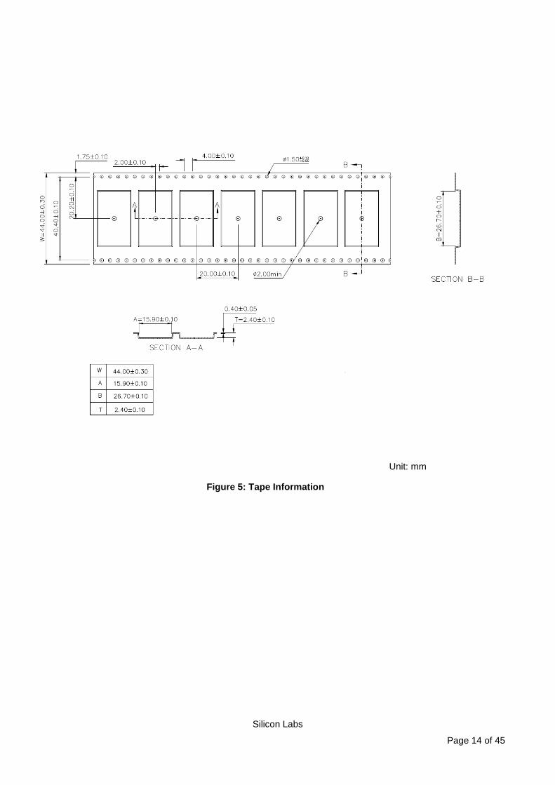
Figure 5: Tape Information
Unit: mm

Silicon Labs
Page 15 of 45
5 Power control
5.1 Power supply requirements
WF121 consists of two separate internal blocks, the microcontroller and the radio part. The blocks have separate supply voltage inputs and the microcontroller can disable the radio part supply internally.
WF121 is designed to operate with a 3.3V nominal input voltage supplied to the two supply inputs. The VDD_3.3V pad can be fed with a voltage between 2.3V and 3.6V and is used to power the internal microcontroller. However, when the VDD_3.3V line is below 3.0V, the microcontroller can no longer write to its internal flash memory, and is incapable of updating any settings. The VDD_PA pad can be supplied with a voltage between 2.7V and 4.8V and supplies the RF power amplifier and the internal switch-mode converter powering the Wi-Fi digital core.
In lithium battery powered applications, VDD_PA can be connected directly to the battery, while a regulator is needed to supply the VDD_3.3V with a lower voltage, as needed by the design.
The VDD_PA supply should be capable of providing at least 350mA, though the average consumption of the module will be much less than that. The VDD_3.3V supply will draw a peak current of less than 100mA, not including current drawn from the GPIO pins. The PA supply should preferably be bypassed with a 10 to 100µF capacitor to smooth out the current spikes drawn by the Wi-Fi power amplifier, unless powered by a sufficiently fast regulator. Other bypass capacitors are not needed for either supply line, the module contains the needed supply filtering capacitors.
Note that there are about 20µF worth of ceramic capacitors on the VDD_PA line inside the module. When using low drop linear regulators (LDO) to generate a regulated supply for the VDD_PA line, the stability of the regulator with the low ESR provided by these capacitors should be checked. Many linear regulators (and some switched mode ones) are not stable with ceramic output capacitors.
5.2 Power saving functionality
In Wi-Fi client mode, the WF121 radio core automatically powers on the RF circuitry only when needed. The Wi-Fi core processors support automatic sleep modes when not communicating actively, allowing very low idle consumption. When used as an access point, the radio core must receive constantly and cannot enter sleep modes.
The WF121 main processor automatically enters an idle mode after a timeout period whenever it is not actively executing anything, lowering its consumption to about a third of the full while allowing instant wakeup. When the power saving functions are enabled in the hardware configuration script, the processor will after a pre-set timeout enter a deeper sleep mode to lower the consumption to much lower levels, but will take a few milliseconds to wake up from and needs an interrupt to wake up.
In applications where small amounts of data are transferred often, consumption can be optimized by collecting data into bigger packages and transferring it in a single burst. As every data transfer is followed by a timeout before sleep modes are entered, reducing the number of individual transfers will reduce average consumption.
Keeping the WF121 associated with an access point with the power saving modes enabled will allow relatively fast response times with a low power consumption, but in some applications the consumption can be reduced further. Unassociating the Wi-Fi will allow fast re-association with lower idle consumption in applications where the module needs to transfer data only occasionally, while for applications where the absolute minimum consumption is desired and the communication intervals are long, the Wi-Fi section of the module can be fully powered off by disabling the module internal switch mode converter feeding the Wi-Fi core. Powering the Wi-Fi down fully will require a full reinitialization of the Wi-Fi core, and will take several seconds before associating with an access point.
The power saving modes are user configurable and controllable. For more information see the firmware documentation.

Silicon Labs
Page 16 of 45
5.3 Reset
WF121 can be reset by the MCLR-pin (active low), system power up or the internal brown-out detector.

Silicon Labs
Page 17 of 45
6 Interfaces
6.1 General Purpose I/O pins
To see which GPIOs are multiplexed with which features, please refer to Table 2.
WF121 contains a number of pads that can be configured to be used as general purpose digital IO’s, analog inputs or for various built-in functions. Provided functions include a Full Speed USB-OTG port, three I2C-ports, two SPI-ports, two UART’s, Ethernet MAC with RMII connection and various timer functions. Some of the pads are 5V tolerant. All GPIO pads can drive currents of up to +/- 25 mA.
Note: In any application, GPIO pins not reserved for a certain function and not driven to some known state by outside circuitry should be set up as outputs by the application software. Only the Change Notice (CN) capable pins have pullup capability, and if the rest of the pins are left as inputs, they will be floating at a voltage between ground and supply voltage, causing increased module power consumption due to leakages.
6.2 Serial ports
Pad number UART 1 UART 2
17 nCTS
19 nRTS
29 TX (output)
32 RX (input)
35 RX
36 TX
44 nCTS (input)
47 nRTS (output)
Table 3: Serial port pads
Two UARTs are provided with RTS/CTS-handshaking. Wired speeds up to 20 Mbps are possible, but the higher bit rates (above 115200 bps) will require the use of an external crystal on OSC1/OSC2 for sufficient clock accuracy. The serial ports can also be used as host connections when using an external microcontroller.
To see what other functions are present on the same pins, please refer to Table 2.

Silicon Labs
Page 18 of 45
6.3 I2C/SPI
Pad number I2C SPI
17 SS4 – Slave select SPI 4
19 SCK4 - Clock SPI 4
29 SCL3 – Clock I2C 3 SDO3 – Data out SPI 3
32 SDA3 – Data I2C 3 SDI3 – Data in SPI 3
35 SDA5 – Data I2C 5 SDI4 – Data in SPI 4
36 SCL5 – Clock I2C 5 SDO4 – Data out SPI 4
44 SDA1 – Data I2C 1 SS3 – Slave select SPI 3
46 SCL1 – Clock I2C 1
47 SCK3 – Clock SPI 3
Table 4: Pads for I2C and SPI
Up to three I2C-ports and up to two SPI ports can be implemented, mostly multiplexed on the same pins together and with the UART signals. The I2C ports support 100 kHz and 400 kHz speed specifications including automatic clock stretching, while the SPI can be operated at up to 20 Mbps. The SPI ports are also available for use as a host connection for use with an external microcontroller. The SPI bus can be configured for any clock phase combination.
For details on the SPI/I2C hardware, please refer to Microchip documentation on SPI and I2C.
To see what other functions are present on the same pins, please refer to Table 2.
6.4 USB
Pad number Function Description
18 OTG_ID USB-OTG mode identify line (not used)
25 VBUS USB bus supply input
27 D- Data -
28 D+ Data +
24 VBUSON USB bus supply switch enable (not used)
Table 5: USB pads
The module contains a USB-OTG system with an integrated transceiver. Full Speed (12 Mbps) USB 2.0 standard is supported in device mode. The current firmware has no support for the host mode.
Using the USB connection requires an external crystal on OSC1/OSC2 for sufficient clock accuracy.

Silicon Labs
Page 19 of 45
Other functions are present on the same pins; please refer to Table 2 for details.
6.5 Ethernet
Pad number Function Description
2 EMDC Management bus clock
3 ERXD1 Receive data 1
4 ERXD0 Receive data 0
5 ECRSDV Receive data valid
6 EREFCLK Reference clock
7 ERXERR Receive error
10 ETXEN Transmit enable
11 ETXD0 Transmit data 0
12 ETXD1 Transmit data 1
42 ETXERR Transmit error
47 EMDIO Management bus data
Table 6: Ethernet pads
An RMII interface to an external Ethernet PHY is available. The PHY should supply EREFCLK with a 50 MHz RMII reference clock. Other functions are present on the same pads; please refer to Table 2 for details.
The current firmware contains support for using a Micrel PHY type KSZ8081RNA (the evaluation board schematic shows the fully compatible but now obsolete KSZ8031RNL) to implement a 10/100Mbps Ethernet connection and using it as an endpoint, allowing data to be streamed from and to the Wi-Fi interface or other end points.
Ethernet MAC-to-MAC connection is also supported using an Ethernet switch chip. Notices: If MDIO is not required, place a 1-10 kohm pull-up resistor on the EMDIO line and don’t wire it to Ethernet chip.
An RMII bus clock (50 MHz) must be fed to EREFCLK from an external clock source, Ethernet PHY or from an Ethernet switch chip.

Silicon Labs
Page 20 of 45
6.6 Analog inputs
Pad number Function
2 AN15
14 AN1
15 AN0
17 AN8
19 AN14
20 AN13
21 AN12
22 AN11
23 AN10
24 AN5
Table 7: ADC pads
The microcontroller provides a 10-bit Analog to digital converter (ADC) with sampling speeds up to 1MSps. The measurement can be done on any of the input pins listed in the table above.
6.7 Microcontroller programming interface
Pad number Pad function Description
13 MCLR Reset
14 PGEC1 Programming Clock
15 PGED1 Programming Data
20 TDI JTAG Test Data In
21 TCK JTAG Test Clock
22 TDO JTAG Test Data out
23 TMS JTAG Test Machine State
Table 8: Programming and JTAG pads
An ICSP (In-Circuit Serial Programming) interface (PGEC1, PGED1, MCLR) is provided to allow device re-flashing using a Microchip tool. A JTAG connection is also provided which can be used for system debugging purposes or device programming. For information on JTAG operation, please refer to Microchip documentation.

Silicon Labs
Page 21 of 45
6.8 RF Debug Interface
Pad number Pad function Description
52 SPI_MISO RF Debug data out
53 SPI_CLK RF Debug clock
54 SPI_MOSI RF Debug data in
55 SPI_CS RF Debug chip select
Table 9: RF Debug SPI pads
Four pads are provided for the debug interface of the WiFi chipset in the module bottom. This is meant for RF calibration and testing during module production and product certification measurements. These should in most applications be left unconnected, but should be taken into account when doing the application board layout. Avoid placing vias or signals without a solder mask under these pads. If separate radiated emission compliance measurements need to made for the application, these should be connected to a header. More information on the certification measurements can be obtained from support via http://www.silabs.com/.
6.9 CPU Clock
Pad number Function Description
30 OSC1 External crystal input
31 OSC2 External crystal output
Table 10: Clock crystal pads
WF121 uses an internal 26 MHz crystal as the WiFi reference clock. The internal processor uses an integrated 8 MHz RC oscillator and associated phase locked loop (PLL) to create its clock signals, but cannot share the internal crystal-stabilized WiFi clock. The internal CPU uses a PLL to create an 80 MHz core clock.
To use the USB functionality or when using the UART with speeds above 115.2 kbps, an external crystal and the associated capacitors must be connected to pads OSC1 and OSC2 to provide a sufficiently accurate clock. Typically the load capacitors should be 22 to 33 pF. If an external crystal is not needed, these pads are available for GPIO use.
For firmware versions lower than 1.3, the external crystal frequency must be 8 MHz, for version 1.3 and later, the frequency should be a multiple of 4 MHz, with a maximum frequency of 24 MHz. The desired frequency can be set in the hardware configuration file and programmed to the module with the firmware.
Due to the protected nature of the oscillator divider settings, the crystal frequency cannot be programmed using the DFU interface. A PICkit3 or other PIC32 compatible programmer is required.
The WF121 with the default settings will detect the presence of an 8 MHz crystal and will use that, or if missing, will automatically use the internal RC oscillator. If the crystal frequency is set to a different frequency in the hardware configuration file, the autodetect will be disabled.
The Ethernet connection requires the external PHY to provide the 50 MHz RMII reference clock. A separate external crystal is not required for the module CPU for Ethernet operation, the internal RC oscillator is sufficient.
Silicon Labs
Page 22 of 45
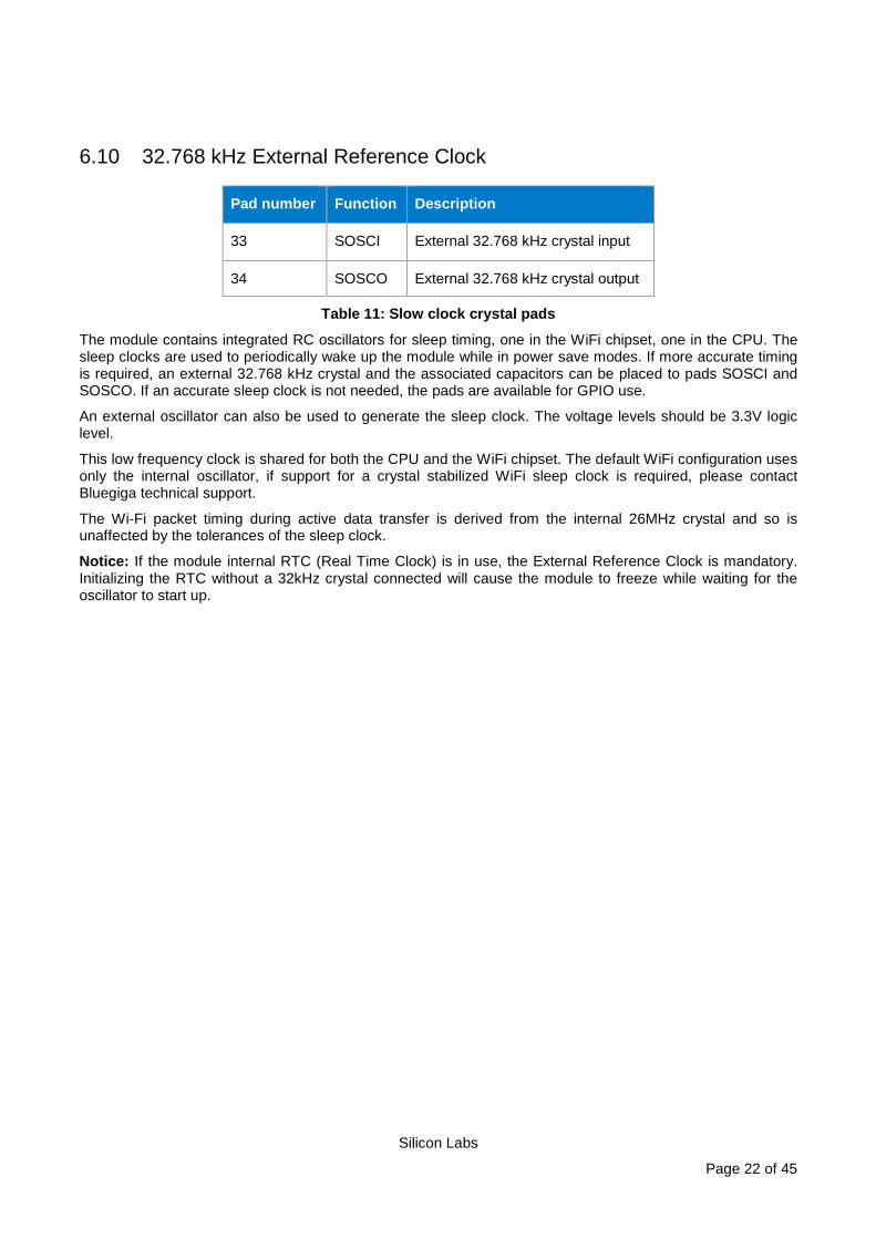
6.10 32.768 kHz External Reference Clock
Pad number Function Description
33 SOSCI External 32.768 kHz crystal input
34 SOSCO External 32.768 kHz crystal output
Table 11: Slow clock crystal pads
The module contains integrated RC oscillators for sleep timing, one in the WiFi chipset, one in the CPU. The sleep clocks are used to periodically wake up the module while in power save modes. If more accurate timing is required, an external 32.768 kHz crystal and the associated capacitors can be placed to pads SOSCI and SOSCO. If an accurate sleep clock is not needed, the pads are available for GPIO use.
An external oscillator can also be used to generate the sleep clock. The voltage levels should be 3.3V logic level.
This low frequency clock is shared for both the CPU and the WiFi chipset. The default WiFi configuration uses only the internal oscillator, if support for a crystal stabilized WiFi sleep clock is required, please contact Bluegiga technical support.
The Wi-Fi packet timing during active data transfer is derived from the internal 26MHz crystal and so is unaffected by the tolerances of the sleep clock.
Notice: If the module internal RTC (Real Time Clock) is in use, the External Reference Clock is mandatory. Initializing the RTC without a 32kHz crystal connected will cause the module to freeze while waiting for the oscillator to start up.

Silicon Labs
Page 23 of 45
7 Block diagram
Silicon Labs
Page 24 of 45
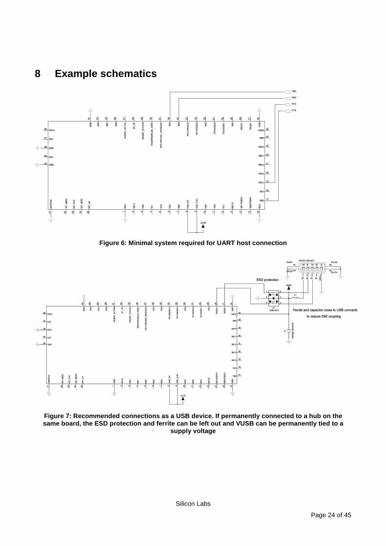
8 Example schematics
Figure 6: Minimal system required for UART host connection
Figure 7: Recommended connections as a USB device. If permanently connected to a hub on the same board, the ESD protection and ferrite can be left out and VUSB can be permanently tied to a
supply voltage
Silicon Labs
Page 25 of 45
9 802.11 Radio
9.1 Wi-Fi Receiver
The receiver features direct conversion architecture. Sufficient out-of-band blocking specification at the Low Noise Amplifier (LNA) input allows the receiver to be used in close proximity to GSM and WCDMA cellular phone transmitters without being desensitized. High-order baseband filters ensure good performance against in-band interference.
9.2 Wi-Fi Transmitter
The transmitter features a direct IQ modulator. Digital baseband transmit circuitry provides the required spectral shaping and on-chip trims are used to reduce IQ modulator distortion. Transmitter gain can be controlled on a per-packet basis, allowing the optimization of the transmit power as a function of modulation scheme.
The internal Power Amplifier (PA) has a maximum output power of +15dBm for IEEE 802.11g/n and +17dBm for IEEE 802.11b. The module internally compensates for PA gain and reference oscillator frequency drifts with varying temperature and supply voltage.
9.3 Regulatory domains
WF121 uses the IEEE 802.11d standard to select the available channels based on the regulatory domain setting of the access point, if enabled. If no domain information is available, WF121 will default to using FCC channel list.
Silicon Labs
Page 26 of 45
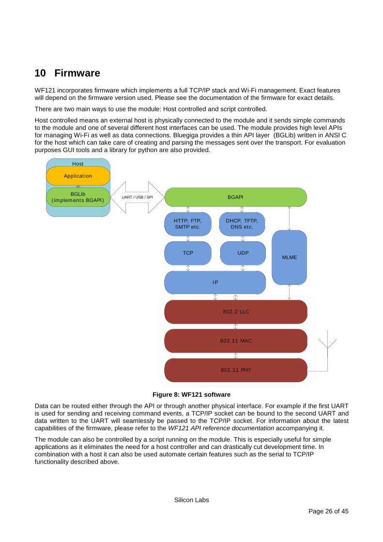
10 Firmware WF121 incorporates firmware which implements a full TCP/IP stack and Wi-Fi management. Exact features will depend on the firmware version used. Please see the documentation of the firmware for exact details.
There are two main ways to use the module: Host controlled and script controlled.
Host controlled means an external host is physically connected to the module and it sends simple commands to the module and one of several different host interfaces can be used. The module provides high level APIs for managing Wi-Fi as well as data connections. Bluegiga provides a thin API layer (BGLib) written in ANSI C for the host which can take care of creating and parsing the messages sent over the transport. For evaluation purposes GUI tools and a library for python are also provided.
IP
BGAPI
802.2 LLC
802.11 MAC
UART / USB / SPI
Host
UDPTCP
BGLib (implements BGAPI)
Application
MLME
802.11 PHY
HTTP, FTP, SMTP etc.
DHCP, TFTP, DNS etc.
Figure 8: WF121 software
Data can be routed either through the API or through another physical interface. For example if the first UART is used for sending and receiving command events, a TCP/IP socket can be bound to the second UART and data written to the UART will seamlessly be passed to the TCP/IP socket. For information about the latest capabilities of the firmware, please refer to the WF121 API reference documentation accompanying it.
The module can also be controlled by a script running on the module. This is especially useful for simple applications as it eliminates the need for a host controller and can drastically cut development time. In combination with a host it can also be used automate certain features such as the serial to TCP/IP functionality described above.
Silicon Labs
Page 27 of 45
11 Host interfaces
11.1 UART
The module can be controlled over the UART interface. In order for the communication to be reliable, hardware flow control signals (RTS and CTS) must be present between the host and the module. When using high UART transfer speeds (between 1 and 20Mbps), an external crystal is required on OSC1/OSC2 for sufficient clock accuracy.
When using WF121 UART in transparent mode, we highly recommend using RTS/CTS flow control to avoid the possibility of losing data.
11.2 USB
When using the USB host interface, the module will appear as a USB CDC/ACM device enumerating as virtual COM port. The same protocol can be used as with the UART interface.
11.3 SPI
Please refer to the Bluegiga WF121 API reference documentation supplied with the firmware regarding using SPI as the host interface. As SPI does not allow the slave device to signal to the master over the bus unless polled, BGAPI over SPI requires the use of an additional “notify” pin which allows the module to notify the host that an outgoing response or event packet is available.
Note: The SPI protocol does not have flow control signaling like UART does, and it is therefore impossible under some circumstances (such as sending very large quantities of data to the module during poor network conditions) to avoid potential data loss due to limited buffer space. If available, the UART interface with hardware RTS/CTS handshaking is recommended for the simplest reliable host control implementation.

Silicon Labs
Page 28 of 45
12 Electrical characteristics
12.1 Absolute maximum ratings
Rating Min Max Unit
Storage Temperature -40 85 °C
VDD_PA -0.3 6 V
VDD_3.3V -0.3 3.6
5V tolerant GPIO Voltages -0.3 5.5 V
Other Terminal Voltages VSS-0.3 VDD_3.3V+0.3 V
Maximum output current sourced or sunk by any GPIO pad 25 mA
Maximum current on all GPIO pads combined 200 mA
Table 12: Absolute maximum ratings
12.2 Recommended operating conditions
Rating Min Max Unit
Operating Temperature Range * -40 85 °C
VDD_3.3V 2.3 3.6 V
VDD_3.3V while capable of writing internal flash 3.0 3.6 V
VDD_PA 2.7 4.8 V
Table 13: Recommended operating conditions
*Note: The module may heat up depending on use, at high constant transmit duty cycles (high throughput, low bitrate for more than a few seconds) the maximum operating temperature may need to be derated to keep below the maximum ratings.

Silicon Labs
Page 29 of 45
12.3 Input/output terminal characteristics
12.4 Digital
Digital terminals Min Typ Max Unit
Input voltage levels
VIL input logic level low 1.7V ≤ VDD ≤ 3.6V VSS-0.3V - 0.15VDD V
VIH input logic level high 1.7V ≤ VDD ≤ 3.6V 0.8VDD - VDD+0.3V V
Output voltage levels
VOL output logic level low, Vdd = 3.6 V, Iol = 7 mA - - 0.4 V
VOH output logic level high Vdd = 3.6 V, Ioh = -12 mA 2.4 - VDD V
Table 14: Digital terminal electrical characteristics
Min Typ max
Frequency 32.748 32.768 32.788 kHz
Deviation @25oC -20 +20 ppm
Deviation over temperature -150 +150 ppm
Duty cycle 30 50 70 %
Rise time 50 ns
Input high level 0.625Vdd Vdd+0.3 V
Input low level -0.3 0.25Vdd V
Table 15: External Wi-Fi sleep clock specifications
12.5 Reset
Power-on Reset Min Typ Max Unit
Power on reset threshold 1.75 - 2.1 V
VDD rise rate to ensure reset 0.05 - 115 V/ms
Table 16: Power on reset characteristics
Silicon Labs
Page 30 of 45
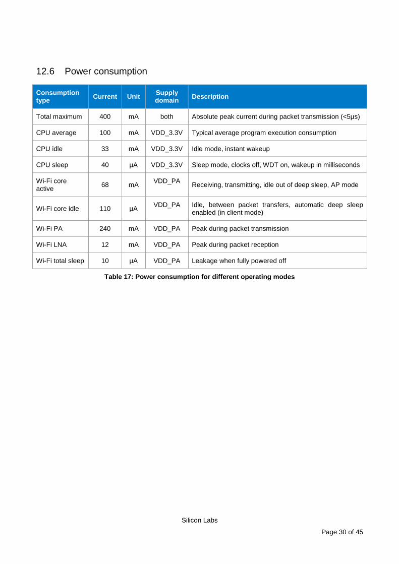
12.6 Power consumption
Consumption type Current Unit Supply
domain Description
Total maximum 400 mA both Absolute peak current during packet transmission (<5µs)
CPU average 100 mA VDD_3.3V Typical average program execution consumption
CPU idle 33 mA VDD_3.3V Idle mode, instant wakeup
CPU sleep 40 µA VDD_3.3V Sleep mode, clocks off, WDT on, wakeup in milliseconds
Wi-Fi core active 68 mA VDD_PA Receiving, transmitting, idle out of deep sleep, AP mode
Wi-Fi core idle 110 µA VDD_PA Idle, between packet transfers, automatic deep sleep enabled (in client mode)
Wi-Fi PA 240 mA VDD_PA Peak during packet transmission
Wi-Fi LNA 12 mA VDD_PA Peak during packet reception
Wi-Fi total sleep 10 µA VDD_PA Leakage when fully powered off
Table 17: Power consumption for different operating modes

Silicon Labs
Page 31 of 45
Consumption type Current Unit Description
Transmit consumption 143 mA Typical average module consumption during full rate data transfer, system does not enter deep sleep due to constant data traffic (Ethernet MAC enabled for testing)
Receive consumption 127 mA Typical average module consumption during full rate data transfer, system does not enter deep sleep due to constant data traffic
Access point mode 108 mA Typical average idle current when configured as an AP, does not enter deep sleep due to AP mode requirements
Idle, associated 1.7-10 mA
Typical average with DTIM=1, beacon interval=100ms, including keep-alive traffic and CPU timed wakeups, power saving enabled (typically 1.7mA when no broadcast traffic is present)
Idle, associated 35 mA Typical average with DTIM=1, beacon interval=100ms, including keep-alive traffic and CPU timed wakeups, power saving disabled
Idle, unassociated 166 µA
Typical sleep current with Wi-Fi chip on and initialized but unassociated. Associating to an access point from this state usually happens in less than a second, depending on DHCP/static IP settings and security options. Peripherals disabled.
Deep Sleep 55 µA
Deep sleep (Wi-Fi power supply disabled internally, CPU sleeping, all peripherals except watchdog and GPIO interrupts off). Waking the Wi-Fi from this state requires reinitialization of the Wi-Fi core and the time from wakeup to access point association can take up to 10 seconds
Table 18: Typical power consumption, module total
All average readings are made with a 3.3V power supply, using the DKWF121 board and comparing Fluke 289 True RMS multimeter average readings with oscilloscope derived mode-specific consumption profiles. Measuring currents varying several orders of magnitude within microseconds may give varying results with different instruments and the measurement method should be considered carefully.
Associated idle consumption is heavily dependent on the access point used, the local broadcast traffic, power save timeouts set by the user and enabled peripherals. Transmit and receive consumptions are heavily dependent on the RF field strength and thus the over-air bitrate, which determines the time taken to transfer the required data. WF121 automatically enters power saving modes when not actively transferring data, and the shorter the time taken to transfer data over the Wi-Fi, the more time it can spend in power saving modes.

Silicon Labs
Page 32 of 45
13 RF Characteristics
min max
Channel 1 11 (default), 13 (ETSI)
Frequency 2412 2472 MHz
Table 19: Supported frequencies
Standard Supported bit rates
802.11b 1, 2, 5.5, 11Mbps
802.11g 6, 9, 12, 18, 24, 36, 48, 54Mbps
802.11n, HT, 20MHz, 800ns 6.5, 13, 19.5, 26, 39, 52, 58.5, 65Mbps
802.11n, HT, 20MHz, 400ns 7.2, 14.4, 21.7, 28.9, 43.3, 57.8, 65, 72.2Mbps
Table 20: Supported modulations
802.11b Typ 802.11g Typ 802.11n short GI Typ 802.11n long GI Typ
1 Mbps -97 dBm 6 Mbps -92 dBm 6.5 Mbps -91 dBm 7.2 Mbps -92 dBm
2 Mbps -95 dBm 9 Mbps -91 dBm 13 Mbps -87 dBm 14.4 Mbps -90 dBm
5.5 Mbps -93 dBm 12 Mbps -89 dBm 19.5 Mbps -85 dBm 21.7 Mbps -87 dBm
11 Mbps -89 dBm 18 Mbps -87 dBm 26 Mbps -82 dBm 28.9 Mbps -84 dBm
24 Mbps -84 dBm 39 Mbps -78 dBm 43.3 Mbps -80 dBm
36 Mbps -80 dBm 52 Mbps -74 dBm 57.8 Mbps -75 dBm
48 Mbps -75 dBm 58.5 Mbps -71 dBm 65 Mbps -72 dBm
54 Mbps -73 dBm 65 Mbps -68 dBm 72.2 Mbps -69 dBm
Table 21: Typical receiver sensitivity

Silicon Labs
Page 33 of 45
Modulation type Typ
802.11b +16 dBm
802.11g +14 dBm
802.11n +14 dBm
Table 22: Transmitter output power at maximum setting
Modulation type Min Typ Max
TX loss -2.5 -3 -3.5 dB
RX gain (using internal LNA) 8 10 12 dB
Internal LNA noise figure 2.0 2.5 dB
Table 23: BT antenna sharing interface properties
Typ Max 802.11 limit (total error)
Variation between individual units +/-5 +/-10 +/-25 ppm
Variation with temperature +/-3 +/-10 +/-25 ppm
Table 24: Carrier frequency accuracy

Silicon Labs
Page 34 of 45
14 Physical dimensions
Figure 9: Physical dimensions
Figure 10: WF121-A recommended PCB land pattern
Silicon Labs
Page 35 of 45
15 Layout guidelines
15.1 WF121-E
RF output can be taken directly from the U.FL connector of the module, and no antenna clearances need to be made for the module.
15.2 WF121-N
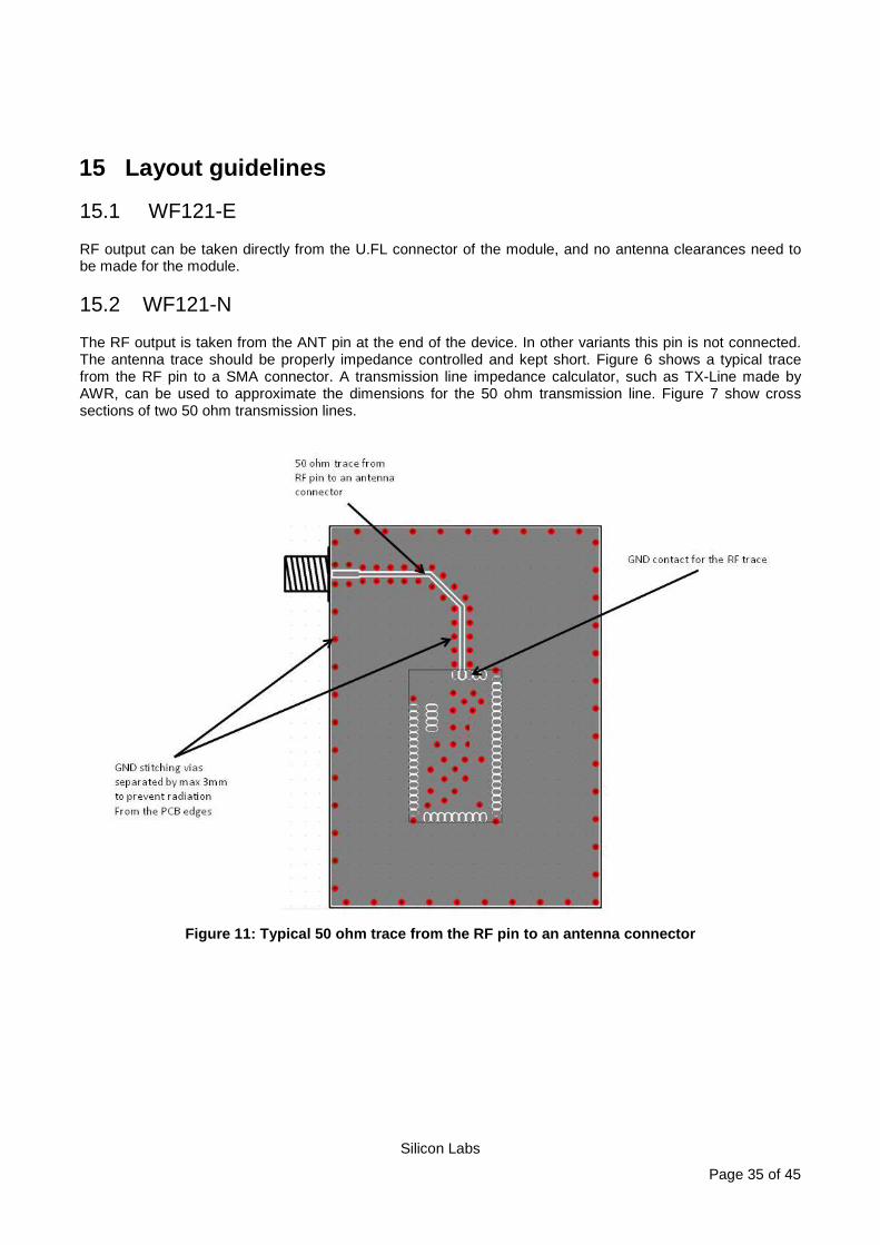
The RF output is taken from the ANT pin at the end of the device. In other variants this pin is not connected. The antenna trace should be properly impedance controlled and kept short. Figure 6 shows a typical trace from the RF pin to a SMA connector. A transmission line impedance calculator, such as TX-Line made by AWR, can be used to approximate the dimensions for the 50 ohm transmission line. Figure 7 show cross sections of two 50 ohm transmission lines.
Figure 11: Typical 50 ohm trace from the RF pin to an antenna connector

Silicon Labs
Page 36 of 45
FR4, εr = 4.6
Prepreg, εr = 3.7
W = 0.15 mm
h = 0.076 mm
G = 0.25 mm
GND stitching vias
RF GROUND
RF GROUND RF GROUND
RF GROUND
FR4, εr = 4.6 h = 1 mm
W = 1.8 mm
MICROSTRIP
CPW Ground
Figure 12: Example cross section of two different 50 ohm transmission line
15.3 WF121-A
Figure 13: Example layouts, board edge placement on left, board corner on right
The impedance matching of the antenna is designed for a layout similar to the module evaluation board. For an optimal performance of the antenna the layout should strictly follow the layout example shown in the above figures and the thickness of FR4 should be between 1 and 2 mm, preferably 1.6mm.
Any dielectric material close to the antenna will change the resonant frequency and it is recommended not to place a plastic case or any other dielectric closer than 5 mm from the antenna. Close proximity of a plastic case can be somewhat compensated by using a thinner PCB.
Silicon Labs
Page 37 of 45
ANY metal in close proximity of the antenna will prevent the antenna from radiating freely. It is recommended not to place any metal or other conductive objects closer than 20 mm to the antenna except in the directions of the ground planes of the module itself.
For optimal performance, place the antenna end of the module outside any metal surfaces and objects in the application, preferably on the device corner. The larger the angle in which no metallic object obstructs the antenna radiation, the better the antenna will work.
The ANT pad on the antenna end of the WF121-A can be connected to the ground or left unsoldered.
15.4 Thermal considerations
The WF121 module may at continuous full power transmit consume up to 1.3 W of DC power, most of which is drawn by the power amplifier. Most of this will be dissipated as heat. In any application where high ambient temperatures and constant transmissions for more than a few seconds can occur, it is important that a sufficient cooling surface is provided to dissipate the heat.
The thermal pad in the bottom of the module must be connected to the application board ground planes by soldering. The application board should provide a number of vias under and around the pad to conduct the produced heat to the board ground planes, and preferably to a copper surface on the other side of the board in order to dissipate the heat into air.
The module internal thermal resistance should in most cases be negligible compared to the thermal resistance from the module into air, and common equations for surface area required for cooling can be used to estimate the temperature rise of the module. Only copper planes on the circuit board surfaces with a solid thermal connection to the module ground pad will dissipate heat. For an application with high transmit duty cycles (low bit rate, high throughput, long bursts or constant streaming) the maximum allowed ambient temperature should be reduced due to inherent heating of the module, especially with small fully plastic enclosed applications where heat transfer to ambient air is low due to low thermal conductivity of plastic.
The module measured on the evaluation board exhibits a temperature rise of about 25oC above ambient temperature when continuously transmitting IEEE 802.11b at full power with minimal off-times and no collision detection (a worst case scenario regarding power dissipation). An insufficiently cooled module will rapidly heat beyond operating range in ambient room temperature.
15.5 EMC considerations
Following recommendations helps to avoid EMC problems arising in the design. Note that each design is unique and the following list do not consider all basic design rules such as avoiding capacitive coupling between signal lines. Following list is aimed to avoid EMC problems caused by RF part of the module.
• Do not remove copper from the PCB more than needed. For proper operation the antenna requires a solid ground plane with as much surface area as possible. Use ground filling as much as possible. Connect all grounds together with multiple vias. Do not leave small floating unconnected copper areas or areas connected by just one via, these will act as additional antennas and raise the risk of unwanted radiations.
• Do not place a ground plane underneath the antenna. The grounding areas under the module should be designed as shown in Figure 4.
• When using overlapping ground areas use conductive vias separated max. 3 mm apart at the edge of the ground areas. This prevents RF from penetrating inside the PCB. Use ground vias extensively all over the PCB. All the traces in (and on) the PCB are potential antennas. Especially board edges should have grounds connected together at short intervals to avoid resonances.
• Avoid current loops. Keep the traces with sensitive, high current or fast signals short, and mind the return current path, having a short signal path is not much use if the associated ground path between the ends of the signal trace is long. Remember, ground is also a signal trace. The ground will conduct the same current as the signal path and at the same frequency, power and sensitivity.

Silicon Labs
Page 38 of 45
• Split a ground plane ONLY if you know exactly what you are doing. Splitting the plane may cause more harm than good if applied incorrectly. The ground plane acts as a part of the antenna system. Insufficient ground planes or large separate sensitive signal ground planes will easily cause the coupled transmitted pulses to be AM-demodulated by semiconductor junctions around the board, degrading system performance.
Overlapping GND layers without GND stitching vias
Overlapping GND layers with GND stitching vias shielding the RF energy
Figure 14: Use of stitching vias to avoid emissions from the edges of the PCB

Silicon Labs
Page 39 of 45
16 Soldering recommendations WF121 is compatible with industrial standard reflow profile for Pb-free solders. The reflow profile used is dependent on the thermal mass of the entire populated PCB, heat transfer efficiency of the oven and particular type of solder paste used. Consult the datasheet of particular solder paste for profile configurations.
The following recommendations apply for soldering the module to ensure reliable solder joint and operation of the module after soldering. Since the profile used is process and layout dependent, the optimum profile should be studied case by case. Thus following recommendation should be taken as a starting point guide.
• Refer to technical documentations of particular solder paste for profile configurations
• Avoid using more than one flow.
• Reliability of the solder joint and self-alignment of the component are dependent on the solder volume. Minimum of 150µm stencil thickness is recommended.
• Aperture size of the stencil should be 1:1 with the pad size.
• A low residue, “no clean” solder paste should be used due to low mounted height of the component.
• If the vias used on the application board have a diameter larger than 0.3mm, it is recommended to mask the via holes at the module side to prevent solder wicking through the via holes. Solders have a habit of filling holes and leaving voids in the thermal pad solder junction, as well as forming solder balls on the other side of the application board which can in some cases be problematic.
Silicon Labs
Page 40 of 45
17 Certifications WF121 is compliant to the following specifications:
17.1 CE
WF121 is in conformity with the essential requirements and other relevant requirements of the R&TTE Directive (1999/5/EC). The product is conformity with the following standards and/or normative documents.
• EMC (immunity only) EN 301 489-17 V.2.2.1 in accordance with EN 301 489-1 V1.9.2
• Radiated emissions EN 300 328 V1.9.1
• Safety standards: EN 60950-1:2006 + A11:2009 + A1:2010 + A12:2011 + A2:2013
17.2 FCC and IC
This device complies with Part 15 of the FCC Rules. Operation is subject to the following two conditions:
(1) this device may not cause harmful interference, and
(2) this device must accept any interference received, including interference that may cause undesired operation.
FCC RF Radiation Exposure Statement:
This equipment complies with FCC radiation exposure limits set forth for an uncontrolled environment. End users must follow the specific operating instructions for satisfying RF exposure compliance. This transmitter must not be co-located or operating in conjunction with any other antenna or transmitter. This transmitter is considered as mobile device and should not be used closer than 20 cm from a human body. To allow portable use in a known host class 2 permissive change is required. Please contact support at http://www.silabs.com/ for detailed information.
IC Statements:
This device complies with Industry Canada license-exempt RSS standard(s). Operation is subject to the following two conditions: (1) this device may not cause interference, and (2) this device must accept any interference, including interference that may cause undesired operation of the device.
Under Industry Canada regulations, this radio transmitter may only operate using an antenna of a type and maximum (or lesser) gain approved for the transmitter by Industry Canada. To reduce potential radio interference to other users, the antenna type and its gain should be so chosen that the equivalent isotropically radiated power (e.i.r.p.) is not more than that necessary for successful communication.
If detachable antennas are used:
This radio transmitter (identify the device by certification number, or model number if Category II) has been approved by Industry Canada to operate with the antenna types listed below with the maximum permissible gain and required antenna impedance for each antenna type indicated. Antenna types not included in this list,

Silicon Labs
Page 41 of 45
having a gain greater than the maximum gain indicated for that type, are strictly prohibited for use with this device. See table 25 for the approved antennas for WF121-E and WF121-N.
OEM Responsibilities to comply with FCC and Industry Canada Regulations
The WF121 Module has been certified for integration into products only by OEM integrators under the following conditions:
• The antenna(s) must be installed such that a minimum separation distance of 20cm is maintained between the radiator (antenna) and all persons at all times.
• The transmitter module must not be co-located or operating in conjunction with any other antenna or transmitter.
As long as the two conditions above are met, further transmitter testing will not be required. However, the OEM integrator is still responsible for testing their end-product for any additional compliance requirements required with this module installed (for example, digital device emissions, PC peripheral requirements, etc.).
IMPORTANT NOTE: In the event that these conditions cannot be met (for certain configurations or co-location with another transmitter), then the FCC and Industry Canada authorizations are no longer considered valid and the FCC ID and IC Certification Number cannot be used on the final product. In these circumstances, the OEM integrator will be responsible for re-evaluating the end product (including the transmitter) and obtaining a separate FCC and Industry Canada authorization.
End Product Labeling
The WF121 Module is labeled with its own FCC ID and IC Certification Number. If the FCC ID and IC Certification Number are not visible when the module is installed inside another device, then the outside of the device into which the module is installed must also display a label referring to the enclosed module. In that case, the final end product must be labeled in a visible area with the following:
“Contains Transmitter Module FCC ID: QOQWF121”
“Contains Transmitter Module IC: 5123A-BGTWF121”
or
“Contains FCC ID: QOQWF121
“Contains IC: 5123A-BGTWF121”
The OEM of the WF121 Module must only use the approved antenna(s) described in table 25, which have been certified with this module.
The OEM integrator has to be aware not to provide information to the end user regarding how to install or remove this RF module or change RF related parameters in the user manual of the end product.
To comply with FCC and Industry Canada RF radiation exposure limits for general population, the antenna(s) used for this transmitter must be installed such that a minimum separation distance of 20cm is maintained between the radiator (antenna) and all persons at all times and must not be co-located or operating in conjunction with any other antenna or transmitter.

Silicon Labs
Page 42 of 45
17.2.1 FCC et IC
Cet appareil est conforme à l’alinéa 15 des règles de la FCC. Deux conditions sont à respecter lors de
son utilisation :
(1) cet appareil ne doit pas créer d’interférence susceptible de causer un quelconque dommage et,
(2) cet appareil doit accepter toute interférence, quelle qu’elle soit, y compris les interférences
susceptibles d’entraîner un fonctionnement non requis.
Déclaration de conformité FCC d’exposition aux radiofréquences (RF):
Ce matériel respecte les limites d’exposition aux radiofréquences fixées par la FCC dans un environnement
non contrôlé. Les utilisateurs finaux doivent se conformer aux instructions d’utilisation spécifiées afin de
satisfaire aux normes d’exposition en matière de radiofréquence. Ce transmetteur ne doit pas être installé ni
utilisé en concomitance avec une autre antenne ou un autre transmetteur. Ce transmetteur est assimilé à un
appareil mobile et ne doit pas être utilisé à moins de 20 cm du corps humain. Afin de permettre un usage
mobile dans le cadre d’un matériel de catégorie 2, il est nécessaire de procéder à quelques adaptations. Pour
des informations détaillées, veuillez contacter le support technique: http://www.silabs.com/.
Déclaration de conformité IC :
Ce matériel respecte les standards RSS exempt de licence d’Industrie Canada. Son utilisation est soumise
aux deux conditions suivantes :
(1) l’appareil ne doit causer aucune interférence, et
(2) l’appareil doit accepter toute interférence, quelle qu’elle soit, y compris les interférences
susceptibles d’entraîner un fonctionnement non requis de l’appareil.
Selon la réglementation d’Industrie Canada, ce radio-transmetteur ne peut utiliser qu’un seul type d’antenne
et ne doit pas dépasser la limite de gain autorisée par Industrie Canada pour les transmetteurs. Afin de
réduire les interférences potentielles avec d’autres utilisateurs, le type d’antenne et son gain devront être
définis de telle façon que la puissance isotrope rayonnante équivalente (EIRP) soit juste suffisante pour
permettre une bonne communication.
Lors de l’utilisation d’antennes amovibles :
Ce radio-transmetteur (identifié par un numéro certifié ou un numéro de modèle dans le cas de la catégorie II)
a été approuvé par Industrie Canada pour fonctionner avec les antennes référencées ci-dessous dans la
limite de gain acceptable et l’impédance requise pour chaque type d’antenne cité. Les antennes non
référencées possédant un gain supérieur au gain maximum autorisé pour le type d’antenne auquel elles
Silicon Labs
Page 43 of 45
appartiennent sont strictement interdites d’utilisation avec ce matériel. Veuillez vous référer au tableau 25
concernant les antennes approuvées pour les WF121.
Les responsabilités de l’intégrateur afin de satisfaire aux réglementations de la FCC et d’Industrie Canada :
Les modules WF121 ont été certifiés pour entrer dans la fabrication de produits exclusivement réalisés par
des intégrateurs dans les conditions suivantes :
• L’antenne (ou les antennes) doit être installée de façon à maintenir à tout instant une distance
minimum de 20cm entre la source de radiation (l’antenne) et toute personne physique.
• Le module transmetteur ne doit pas être installé ou utilisé en concomitance avec une autre antenne
ou un autre transmetteur.
Tant que ces deux conditions sont réunies, il n’est pas nécessaire de procéder à des tests supplémentaires
sur le transmetteur. Cependant, l’intégrateur est responsable des tests effectués sur le produit final afin de se
mettre en conformité avec d’éventuelles exigences complémentaires lorsque le module est installé (exemple :
émissions provenant d’appareils numériques, exigences vis-à-vis de périphériques informatiques, etc.) ;
IMPORTANT : Dans le cas où ces conditions ne peuvent être satisfaites (pour certaines configurations ou
installation avec un autre transmetteur), les autorisations fournies par la FCC et Industrie Canada ne sont plus
valables et les numéros d’identification de la FCC et de certification d’Industrie Canada ne peuvent servir pour
le produit final. Dans ces circonstances, il incombera à l’intégrateur de faire réévaluer le produit final
(comprenant le transmetteur) et d’obtenir une autorisation séparée de la part de la FCC et d’Industrie Canada.
Etiquetage du produit final
Chaque module WF121 possède sa propre identification FCC et son propre numéro de certification IC. Si
l’identification FCC et le numéro de certification IC ne sont pas visibles lorsqu’un module est installé à
l’intérieur d’un autre appareil, alors l’appareil en question devra lui aussi présenter une étiquette faisant
référence au module inclus. Dans ce cas, le produit final doit comporter une étiquette placée de façon visible
affichant les mentions suivantes :
« Contient un module transmetteur certifié FCC QOQWF121 »
« Contient un module transmetteur certifié IC 5123A-BGTWF121 »
ou
« Inclut la certification FCC QOQWF121 »

Silicon Labs
Page 44 of 45
« Inclut la certification IC 5123A-BGTWF121 »
L’intégrateur du module WF121 ne doit utiliser que les antennes répertoriées dans le tableau 25 certifiées
pour ce module.
L’intégrateur est tenu de ne fournir aucune information à l’utilisateur final autorisant ce dernier à installer ou
retirer le module RF, ou bien changer les paramètres RF du module, dans le manuel d’utilisation du produit
final.
Afin de se conformer aux limites de radiation imposées par la FCC et Industry Canada, l’antenne (ou les antennes) utilisée pour ce transmetteur doit être installée de telle sorte à maintenir une distance minimum de 20cm à tout instant entre la source de radiation (l’antenne) et les personnes physiques. En outre, cette antenne ne devra en aucun cas être installée ou utilisée en concomitance avec une autre antenne ou un autre transmetteur.

Silicon Labs
Page 45 of 45
18 Qualified Antenna Types for WF121-E This device has been designed to operate with the antennas listed below, and having a maximum gain of 2.14 dB. Antennas not included in this list or having a gain greater than 2.14 dB are strictly prohibited for use with this device. The required antenna impedance is 50 ohms.
Qualified Antenna Types for WT121-E Antenna Type Maximum Gain
Dipole 2.14 dBi
Table 25: Qualified Antenna Types for WF121-E
Any antenna that is of the same type and of equal or less directional gain as listed in Table 25 can be used without a need for retesting. To reduce potential radio interference to other users, the antenna type and its gain should be so chosen that the equivalent isotropically radiated power (e.i.r.p.) is not more than that permitted for successful communication. Using an antenna of a different type or gain more than 2.14 dBi will require additional testing for FCC, CE and IC. Please, contact support at http://www.silabs.com/ for more information.

http://www.silabs.com
Silicon Laboratories Inc.400 West Cesar ChavezAustin, TX 78701USA
Smart. Connected. Energy-Friendly.
Productswww.silabs.com/products
Qualitywww.silabs.com/quality
Support and Communitycommunity.silabs.com
DisclaimerSilicon Labs intends to provide customers with the latest, accurate, and in-depth documentation of all peripherals and modules available for system and software implementers using or intending to use the Silicon Labs products. Characterization data, available modules and peripherals, memory sizes and memory addresses refer to each specific device, and "Typical" parameters provided can and do vary in different applications. Application examples described herein are for illustrative purposes only. Silicon Labs reserves the right to make changes without further notice and limitation to product information, specifications, and descriptions herein, and does not give warranties as to the accuracy or completeness of the included information. Silicon Labs shall have no liability for the consequences of use of the information supplied herein. This document does not imply or express copyright licenses granted hereunder to design or fabricate any integrated circuits. The products are not designed or authorized to be used within any Life Support System without the specific written consent of Silicon Labs. A "Life Support System" is any product or system intended to support or sustain life and/or health, which, if it fails, can be reasonably expected to result in significant personal injury or death. Silicon Labs products are not designed or authorized for military applications. Silicon Labs products shall under no circumstances be used in weapons of mass destruction including (but not limited to) nuclear, biological or chemical weapons, or missiles capable of delivering such weapons.
Trademark InformationSilicon Laboratories Inc.® , Silicon Laboratories®, Silicon Labs®, SiLabs® and the Silicon Labs logo®, Bluegiga®, Bluegiga Logo®, Clockbuilder®, CMEMS®, DSPLL®, EFM®, EFM32®, EFR, Ember®, Energy Micro, Energy Micro logo and combinations thereof, "the world’s most energy friendly microcontrollers", Ember®, EZLink®, EZRadio®, EZRadioPRO®, Gecko®, ISOmodem®, Precision32®, ProSLIC®, Simplicity Studio®, SiPHY®, Telegesis, the Telegesis Logo®, USBXpress® and others are trademarks or registered trademarks of Silicon Labs. ARM, CORTEX, Cortex-M3 and THUMB are trademarks or registered trademarks of ARM Holdings. Keil is a registered trademark of ARM Limited. All other products or brand names mentioned herein are trademarks of their respective holders.