what has changed? technology challenges technology solutions summary
TRANSCRIPT

What has Changed?
Technology Challenges
Technology Solutions
The New Supply Chain
Summary
2
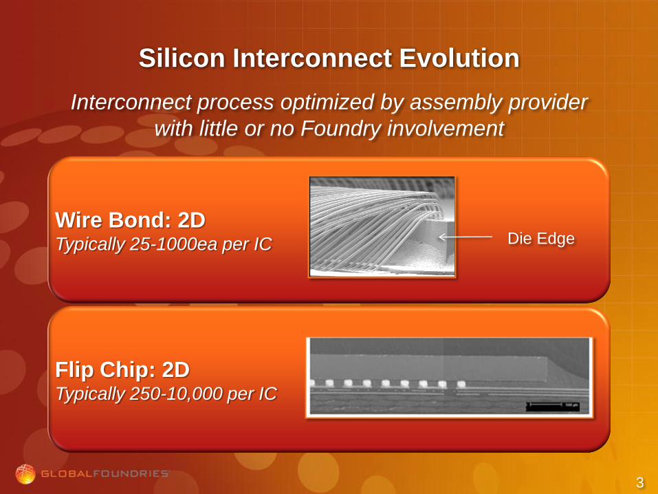
Silicon Interconnect Evolution
Interconnect process optimized by assembly provider
with little or no Foundry involvement
Wire Bond: 2DTypically 25-1000ea per IC Die Edge
Flip Chip: 2DTypically 250-10,000 per IC
3
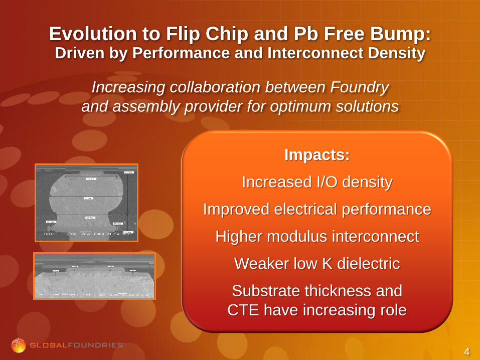
Evolution to Flip Chip and Pb Free Bump:Driven by Performance and Interconnect Density
Increasing collaboration between Foundry
and assembly provider for optimum solutions
Impacts:
Increased I/O density
Improved electrical performance
Higher modulus interconnect
Weaker low K dielectric
Substrate thickness and
CTE have increasing role
4
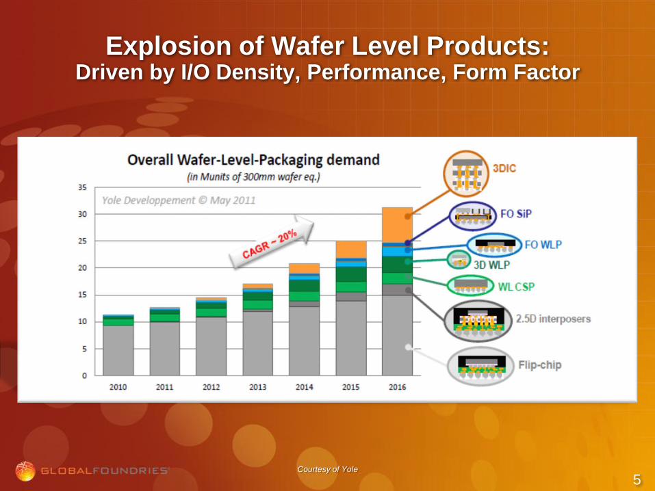
Explosion of Wafer Level Products:Driven by I/O Density, Performance, Form Factor
Courtesy of Yole
5
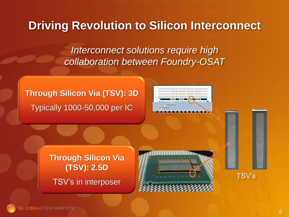
Through Silicon Via (TSV): 3D
Typically 1000-50,000 per IC
Driving Revolution to Silicon Interconnect
Interconnect solutions require high
collaboration between Foundry-OSAT
TSV’s
Through Silicon Via
(TSV): 2.5D
TSV’s in interposer
6

Requiring New Technologies
New interconnect at much finer pitch
Probe (wafer test) as fine pitch
Thin wafer handling
New assembly technologies and
design rules to manage warpage
7

Technology Challenges
Performance
More than
Moore
Power
8

Video and data
packet processing
are driving
need for faster
memory access Graphics,
Mobile Video,
Networking
Processors,
FPGAPower becoming
costly for
performance
and mobile
applications
Power consumed
by logic and
memory reducing
battery lifeIncreasing power
required for logic
and memory
Digital scaling and
performance
(for video/data)
outstripping
memory capacity
System Level
Performance
and Bandwidth
9
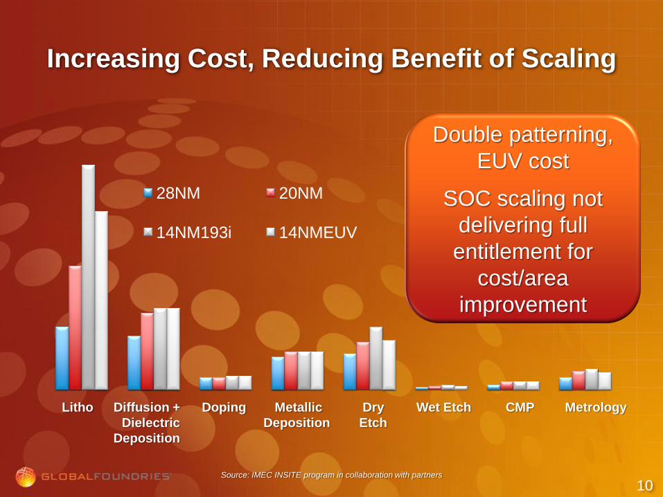
Increasing Cost, Reducing Benefit of Scaling
Source: IMEC INSITE program in collaboration with partners
28NM 20NM
14NM193i 14NMEUV
Litho Diffusion +
Dielectric
Deposition
Doping Metallic
Deposition
Dry
Etch
Wet Etch CMP Metrology
Double patterning,
EUV cost
SOC scaling not
delivering full
entitlement for
cost/area
improvement
10
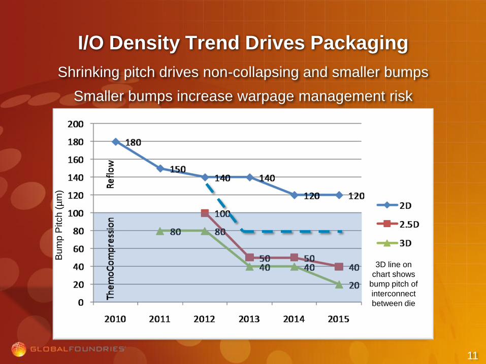
I/O Density Trend Drives Packaging
Shrinking pitch drives non-collapsing and smaller bumps
Smaller bumps increase warpage management risk
3D line on
chart shows
bump pitch of
interconnect
between die
Bu
mp
Pitch
(µ
m)
11

Solutions:Innovation, Cost,
Collaboration
Performance
More than
Moore
Power
12
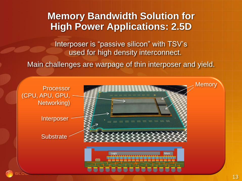
Memory Bandwidth Solution for High Power Applications: 2.5D
Interposer
Processor
(CPU, APU, GPU,
Networking)
Memory
Substrate
MemLogic
Interposer is “passive silicon” with TSV’sused for high density interconnect.
Main challenges are warpage of thin interposer and yield.
13
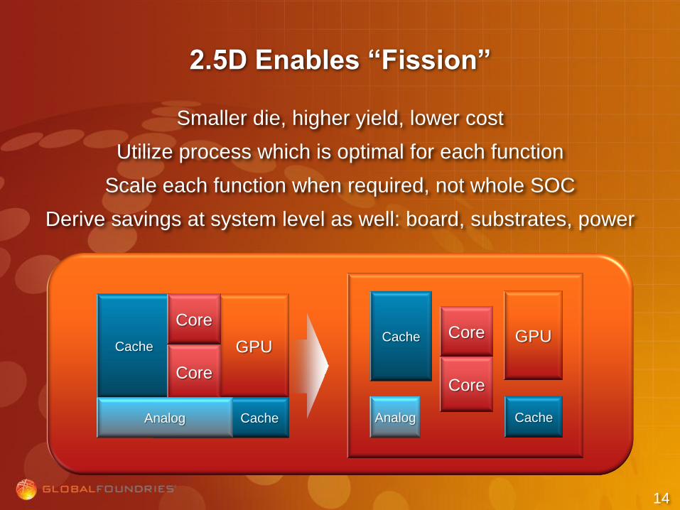
2.5D Enables “Fission”
Cache GPU
Core
Analog Cache
CoreCache GPU
Core
Core
CacheAnalog
Smaller die, higher yield, lower cost
Utilize process which is optimal for each function
Scale each function when required, not whole SOC
Derive savings at system level as well: board, substrates, power
14
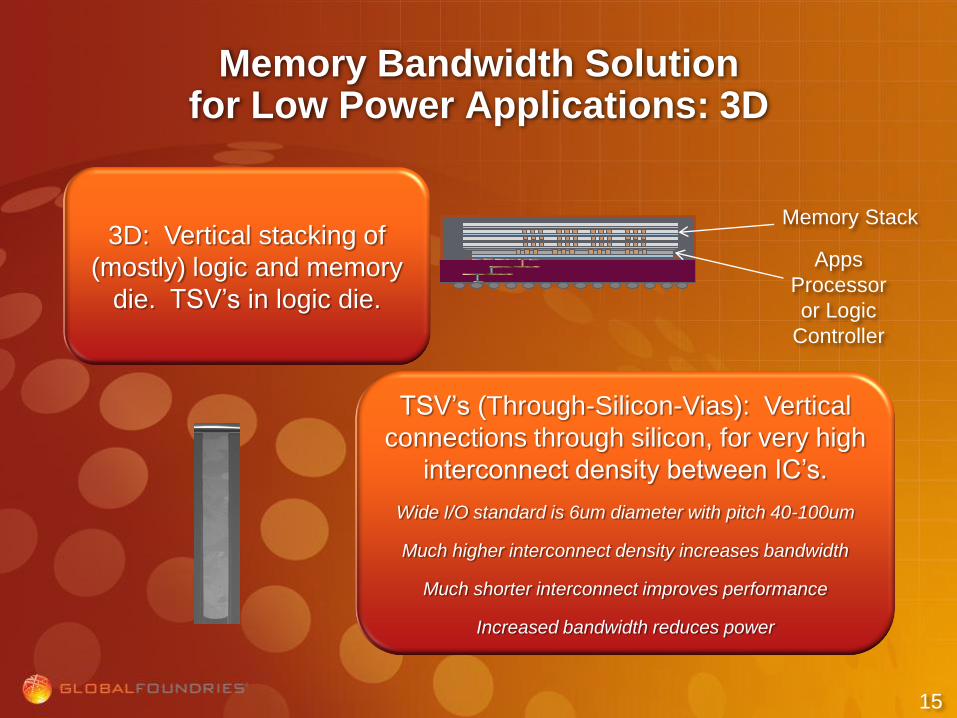
Memory Bandwidth Solution for Low Power Applications: 3D
3D: Vertical stacking of
(mostly) logic and memory
die. TSV’s in logic die.
TSV’s (Through-Silicon-Vias): Vertical
connections through silicon, for very high
interconnect density between IC’s.
Wide I/O standard is 6um diameter with pitch 40-100um
Much higher interconnect density increases bandwidth
Much shorter interconnect improves performance
Increased bandwidth reduces power
Apps
Processor
or Logic
Controller
Memory Stack
15

TSV Formation
Step height measurement for
Cu pumping detection,
Buffer polish and 2nd anneal
can be skipped
16

TSV Process Development
TSV Etch installed, Fab 8, NY
Module
development
at consortia
Integration in
Foundry
Collaboration
between
consortia,
foundry, tool
manufacturer
critical
17

Packaging Roadmap
Silicon
Partitioning
with
Interposers
Market:
FPGA
Memory Cube
Market: Server
and Computing
Logic + Memory
on Interposer
Market:
GPU, CPU,
Network
Processors
Wide I/O
Memory on
Apps
Processor
Market: Mobile,
Tablet
Heterogeneous
Stacking
Market: Mobile,
CPU
RFBasebandProcessor
SensorPMIC
Time
18
2011 2013 2013/14 2014 2017?
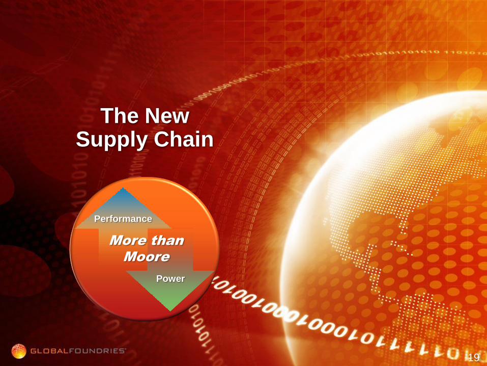
The New Supply Chain
Performance
More than
Moore
Power
19

Why Won’t the Current Model Work?
Solutions developed in isolation are no longer adequate to
address the complexity of high-silicon content packaging
Customer
Com
ponents
Foundry
Bum
p
Assem
bly
Test
20

Solution
optimized to
one product
Best solutions
rarely
originate
from insulated
team
Systems and
methods
become
inflexible
Lack of
transparency
to customer
Single source
supply
Lack of
flexibility and
competition
Why Won’t the Old
IDM Model Work?
21
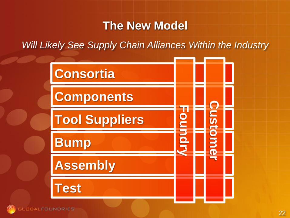
The New Model
Components
Tool Suppliers
Bump
Assembly
Test
Consortia
Fo
un
dry
Cu
sto
mer
Will Likely See Supply Chain Alliances Within the Industry
22

Collaborative Solutions Utilizing the Best Minds
Opt
imiz
e Bl
ock
Plac
emen
t
Opt
imiz
e TS
V/B
ump
Plac
emen
t
PDKs
Refe
renc
e Fl
owTS
V D
evel
opm
ent
TSV
Met
rolo
gyTS
V Im
pact
on
Tran
sist
ors
Thin
ning
Impa
ct o
n Tr
ansi
stor
s
KGD
Met
hods
Fine
Pitc
h Pr
obe
Thin
Waf
er H
andi
ngA
ssem
bly
Dev
elop
men
t
Test
Str
ateg
y an
d IP
Test
Rep
aira
bilit
y
Consortia
Customers
EDA Tool Suppliers
MOL Tool Suppliers
Assm Tool Suppliers
Foundry
OSATs
Memory Suppliers
Test Tool Suppliers
23
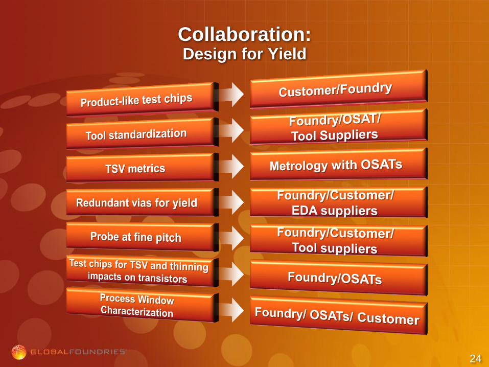
Collaboration:Design for Yield
24

Co-Locate to Develop Solutions for Customers
Bring foundry and partners together to
develop new tools, processes, and
technologies for joining silicon
Fast learning cycles
Develop BEOL, bump, BSI, 3D assembly,
test, and metrology together in one
location for best collaborative ideas and
evaluation of potential solutions
Development of thin wafer (50µm)
handling tools and methods
25
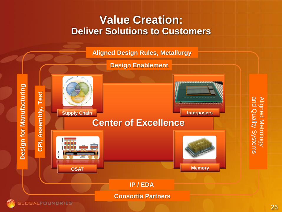
Value Creation:Deliver Solutions to Customers
Center of Excellence
Interposers
MemoryOSAT
Supply Chain
Design Enablement
IP / EDA
CP
I, A
ssem
bly
, T
est
Aligned Design Rules, Metallurgy
Consortia Partners
Desig
n f
or
Man
ufa
ctu
rin
gA
ligned M
etro
logy
and Q
uality
Syste
ms
26
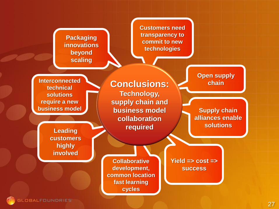
Packaging
innovations
beyond
scaling
Interconnected
technical
solutions
require a new
business model
Leading
customers
highly
involved
Collaborative
development,
common location
fast learning
cycles
Yield => cost =>
success
Supply chain
alliances enable
solutions
Open supply
chain
Customers need
transparency to
commit to new
technologies
Conclusions: Technology,
supply chain and
business model
collaboration
required
27

Thank You
Trademark Attribution
GLOBALFOUNDRIES, the GLOBALFOUNDRIES logo and combinations thereof are trademarks of GLOBALFOUNDRIES Inc. in the United States and/or other jurisdictions. Other names used in this presentation are for identification purposes only and may be trademarks of their respective owners.
©2012 GLOBALFOUNDRIES Inc. All rights reserved.
28