what is an amplifier? - lark.tu-sofia.bg · pdf filewhat is an amplifier? ... (cc) and...
TRANSCRIPT
1
EE141© 2010, Доц.д-р. T.Василева
1
Bipolar Junction Transistor
Amplifiers
Semiconductor
Elements
EE141© 2010, Доц.д-р. T.Василева
2
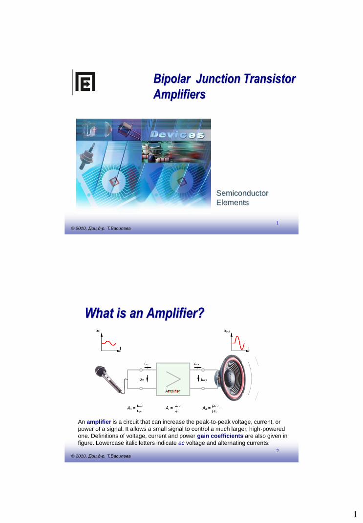
What is an Amplifier?
An amplifier is a circuit that can increase the peak-to-peak voltage, current, or
power of a signal. It allows a small signal to control a much larger, high-powered
one. Definitions of voltage, current and power gain coefficients are also given in
figure. Lowercase italic letters indicate ac voltage and alternating currents.

2
EE141© 2010, Доц.д-р. T.Василева
3
Amplifier Configurations
There are three configurations of a BJT amplifier circuit: common-
emitter (CE), common-collector (CC) and common-base (CB). The
configuration is named for the electrode that is common for input and
output networks. The CE is the most widely used for amplifiers because
it has the best combination of current gain and voltage gain. In CE the
input and output voltage are 180° out of phase, called an inversion.
EE141© 2010, Доц.д-р. T.Василева
4
Transistor Biasing
For the transistor to operate properly as an amplifier, the base-emitter junction
should be forward-biased and the base-collector junction – reverse-biased. This is
called forward-reverse bias. The three dc voltages for the biased transistor are
the emitter voltage UE, the collector voltage UC and the base voltage UB. These
voltages are measured with respect to ground.
Circuit with fixed
base current
3
EE141© 2010, Доц.д-р. T.Василева
5
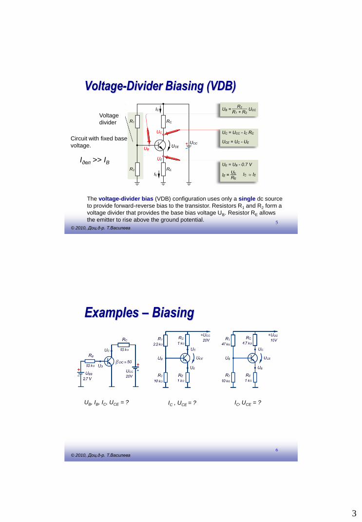
Voltage-Divider Biasing (VDB)
The voltage-divider bias (VDB) configuration uses only a single dc source
to provide forward-reverse bias to the transistor. Resistors R1 and R2 form a
voltage divider that provides the base bias voltage UB. Resistor RE allows
the emitter to rise above the ground potential.
Circuit with fixed base
voltage.
Voltage
divider
Iдел >> IB
EE141© 2010, Доц.д-р. T.Василева
6
Examples – Biasing
IC , UCE = ? IC, UCE = ?UB, IB, IC, UCE = ?
4
EE141© 2010, Доц.д-р. T.Василева
7
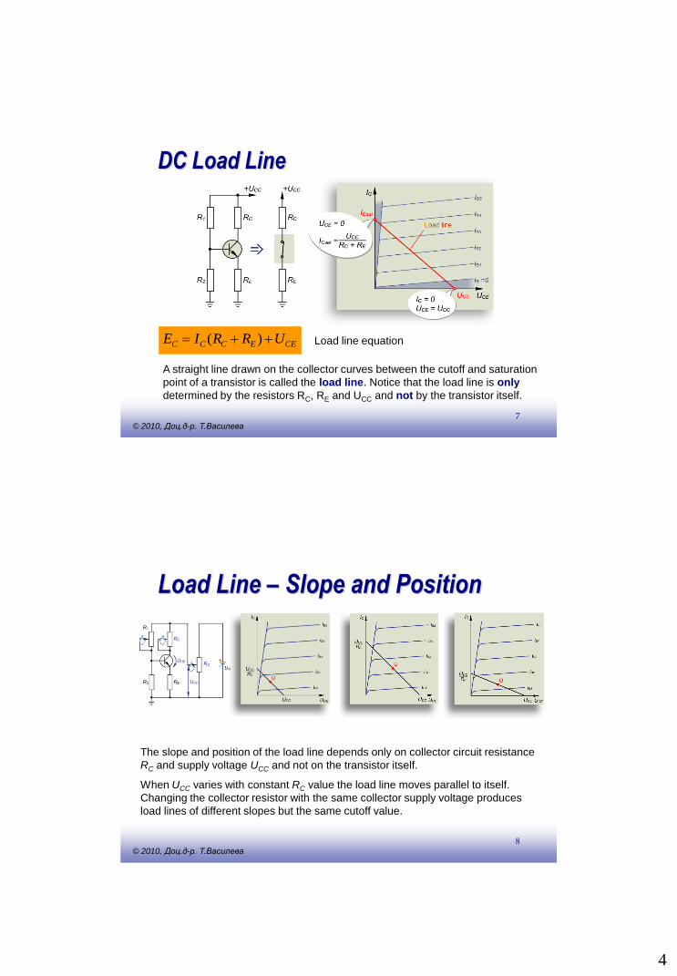
DC Load Line
A straight line drawn on the collector curves between the cutoff and saturation
point of a transistor is called the load line. Notice that the load line is only
determined by the resistors RC, RE and UCC and not by the transistor itself.
CEECCC URRIE )( Load line equation
EE141© 2010, Доц.д-р. T.Василева
8
The slope and position of the load line depends only on collector circuit resistance
RC and supply voltage UCC and not on the transistor itself.
When UCC varies with constant RC value the load line moves parallel to itself.
Changing the collector resistor with the same collector supply voltage produces
load lines of different slopes but the same cutoff value.
Load Line – Slope and Position
5
EE141© 2010, Доц.д-р. T.Василева
9
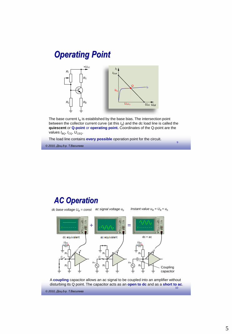
Operating Point
The base current IB is established by the base bias. The intersection point
between the collector current curve (at this IB) and the dc load line is called the
quiescent or Q-point or operating point. Coordinates of the Q-point are the
values IBQ, ICQ, UCEQ.
The load line contains every possible operation point for the circuit.
EE141© 2010, Доц.д-р. T.Василева
10
AC Operationdc base voltage UB = const ac signal voltage ub Instant value uB = UB + ub
Coupling
capacitor
A coupling capacitor allows an ac signal to be coupled into an amplifier without
disturbing its Q point. The capacitor acts as an open to dc and as a short to ac.

6
EE141© 2010, Доц.д-р. T.Василева
11
Signal Operation on the Load Line
The input signal varies the base current above and below its dc value. This
causes much larger variation in the collector current because of the
transistor current gain. The variation in collector current produces a
corresponding variation in the voltage across RC. As a result, the collector-
emitter voltage UCE also changes.
EE141© 2010, Доц.д-р. T.Василева
12
Waveforms & DC Levels
Input and output signal waveforms
An input signal with an amplitude of 50 mV is applied to the CE amplifier.
The output signal is with amplitude of 500 mV. The amplifier voltage gain
Au = 10.
7
EE141© 2010, Доц.д-р. T.Василева
13
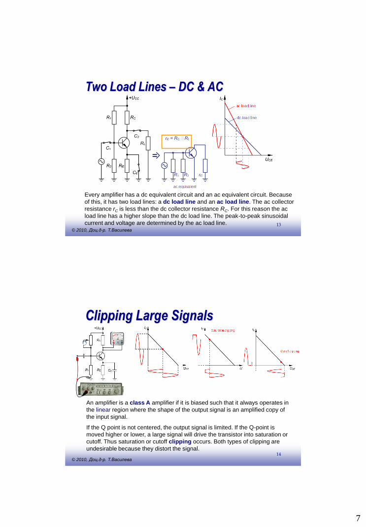
Two Load Lines – DC & AC
Every amplifier has a dc equivalent circuit and an ac equivalent circuit. Because
of this, it has two load lines: a dc load line and an ac load line. The ac collector
resistance rC is less than the dc collector resistance RC. For this reason the ac
load line has a higher slope than the dc load line. The peak-to-peak sinusoidal
current and voltage are determined by the ac load line.
EE141© 2010, Доц.д-р. T.Василева
14
Clipping Large Signals
An amplifier is a class A amplifier if it is biased such that it always operates in
the linear region where the shape of the output signal is an amplified copy of
the input signal.
If the Q point is not centered, the output signal is limited. If the Q-point is
moved higher or lower, a large signal will drive the transistor into saturation or
cutoff. Thus saturation or cutoff clipping occurs. Both types of clipping are
undesirable because they distort the signal.
8
EE141© 2010, Доц.д-р. T.Василева
15
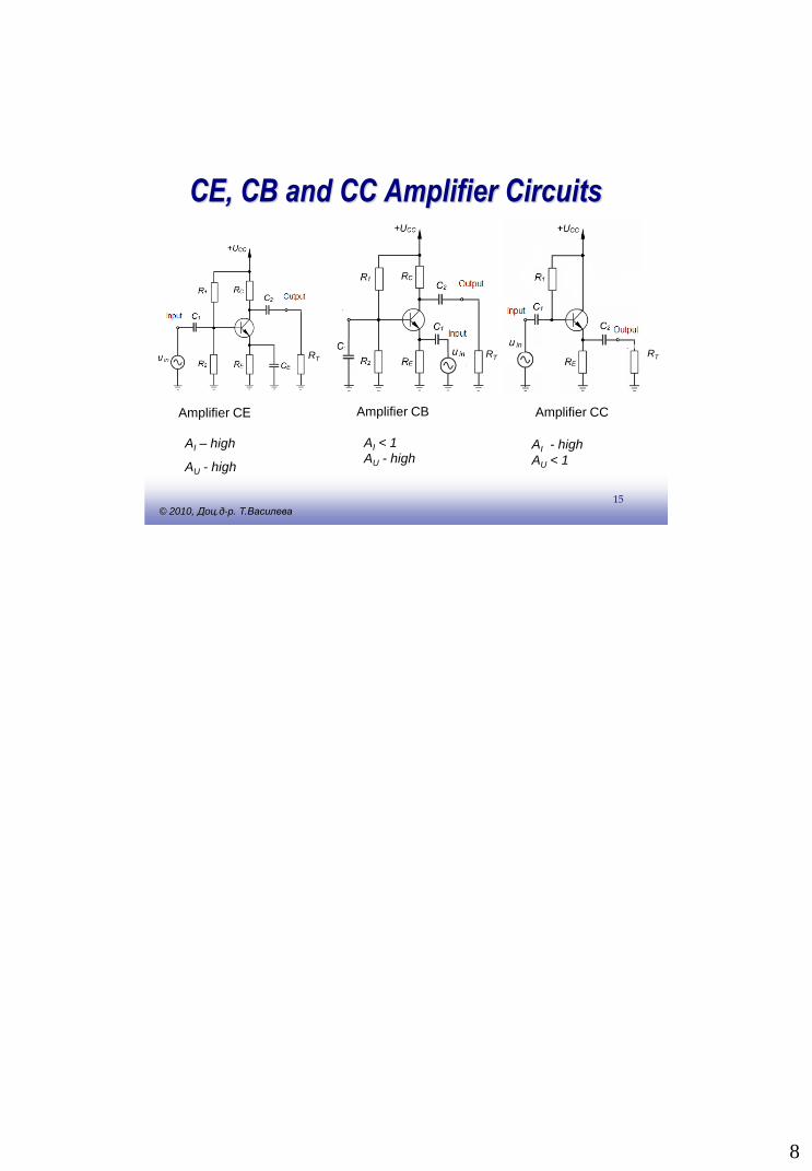
CE, CB and CC Amplifier Circuits
RTRT RT
Amplifier CЕ Amplifier CB Amplifier CC
AI – high
AU - high
AI < 1
AU - highAI - high
AU < 1