white paper - ansys · streaming data and video content, ... tion can be mitigated through the use...
TRANSCRIPT

60 GHz Transceiver IC Design Using High-Mobility .15-micron GaAs Process
wHITe PAPer
�
TABLE OF CONTENTS
Executive Summary ......................................................... 3
Introduction ..................................................................... 4
Millimeter-Wave MMIC Design ...................................... 5
Design Environment ........................................................ 6
Millimeter-Wave Power Amplifier Design Example ...... 9
Conclusion ....................................................................... 17
Appendix ......................................................................... 18
About The Companies .................................................... 19

3
EXECUTIVE SUMMARY
To meet these challenges, Taiyo Yuden chose circuit and electromagnetic field simulation tools from Ansoft to deliver the accuracy, speed, and capacity for modern millimeter-wave design. They chose the United Monolithic Semiconductors (UMS) Pseudomorphic High Electron Mobility Transistor (pHEMT) PH15 gallium arsenide (GaAs) monolithic microwave integrated circuit (MMIC) process due to its high performance and stability.
This document describes new technologies that enable reliable MMIC design at millimeter-wave frequencies. It is shown that successful millimeter-wave MMIC design requires:
• A reliable millimeter-wave integrated circuit process, • A millimeter-wave qualified design kit based on rigorous device modeling and validation, and • Advanced frequency-domain simulation that can handle highly nonlinear and dense integrated circuits.
The 60 GHz frequency is the primary challenge driving the technologies in this work; however, readers will understand that additional precision, capacity, and reliability are key enablers at any frequency, hence the design methods described here can be utilized for added fidelity and design success in microwave applications.
The demand for wireless high-speed data and multimedia local area networking has driven engineers to consider the abundant bandwidth in the 60 GHz millimeter-wave band. Several GHz of unlicensed continuous spectrum has been made available worldwide with sufficient bandwidth to support multi-gigabit data rates previously only available on fiber-optic networks. This bandwidth opens new opportunities to transfer tremendous volumes of data for enterprise, data storage, and entertainment without the need for physical interconnection. Enabling the broad adoption of new electronic systems that take advantage of these opportunities requires high-performance, integrated, and low-cost solutions. A key element of the solution is the development of integrated circuit technology for the millimeter-wave radio circuits.
Japanese electronics manufacturer Taiyo Yuden is engaged in the research and development of integrated 60 GHz transceivers for short range wireless communication. They understand that the high frequencies involved create significant design, simulation, and implementation challenges. Rigorous and highly accurate active and passive device modeling is required to account for all device-level and electromagnetic coupling effects. High integration and millimeter-wave measurement challenges necessitate simulation of entire circuits with a great number of nonlinear devices rather than individual, isolated circuit blocks. Integrated circuit semiconductor process technologies must provide reliable high-frequency performance, and physical circuit layout within design tools must match the semiconductor process precisely.
4
INTRODUCTION
Japanese electronics manufacturer Taiyo Yuden, Euro-pean semiconductor foundry United Monolithic Semi-conductors (UMS), and Ansoft Corporation have teamed to meet the challenges associated with designing integrated circuits at millimeter-wave frequencies. Taiyo Yuden is performing circuit design and layout, Ansoft is providing advanced circuit and electromagnetic design software and design kits, and UMS is providing ad-vanced GaAs MMIC fabrication and test. Development of this solution is valuable for emerging applications of millimeter-waves for very high-speed networking, digital communications, collision avoidance radar, and automatic cruise control systems, all of which benefit from the lower cost solution that integration provides.
The foundation of the design solution is rigorous device modeling and validation resulting in a millimeter-wave qualified design kit. An accurate design kit is essential when designing circuits at these high frequencies to enable engineers to assemble passive and active de-vices into circuits such that subsequent simulations will capture true circuit performance. All design kit elements include schematic plus layout information, and circuits can be designed in either the schematic view or layout view with electromagnetic accuracy included at the component, circuit, and system levels.
Performing laboratory measurements at millimeter-wave frequencies is not trivial. The tiny dimensions of the circuits complicate probe placement, making equipment calibration challenging and measurement repeatability the purview of highly skilled technicians. For these reasons it is desirable to design, simulate, and verify radio circuits including all electromagnetic effects prior to fabrication. Advanced frequency-domain simu-lation that can handle highly nonlinear and dense inte-grated circuits is required to ensure that circuit blocks of the mm-wave radio systems can be simulated accurately. Reliable 60 GHz design is provided by electromagnetic (EM) simulation to extract passive models, more power-ful harmonic balance to allow large, nonlinear blocks to be simulated, and a validated design kit for fully param-eterized design and optimization.
Taiyo Yuden is developing integrated 60 GHz transceiv-ers for short range wireless communication. They se-lected the UMS PH15 GaAs MMIC process due to its high performance and stability. The UMS PH15 offering has a very low noise pseudomorphic HEMT (pHEMT) process that exhibits an FT larger than 110 GHz and a NFmin of 1.9dB noise figure with 6 dB gain at 60 GHz. For the simulator, Taiyo Yuden chose Ansoft Nexxim because of its superior simulation technology in the frequency do-main. Ansoft Japan has formed a project to develop the UMS PH15 layout-driven design kit to enable reliable millimeter-wave MMIC design.
5
MILLIMETER-WAVE MMICDESIGN
Advantages
MMICs operating at mm-wave frequencies offer numer-ous advantages over traditional low-frequency circuits owing to the high integration, wide frequency band-widths and short wavelengths [1]. High levels of inte-gration available using modern GaAs MMIC processes make it possible to integrate entire millimeter-wave transceiver systems on a single chip. This integration in a mainstream process can greatly reduce the cost of implementation and make practical the new opportuni-ties offered by the 60 GHz band.
The mm-wave frequencies offer tremendous capacity, allowing more information to be communicated across a particular channel. The 7-GHz unlicensed band around 60 GHz offers the possibility of data communication at rates of several gigabits per second, opening up new opportunities for high-data-rate wireless Internet access, streaming data and video content, and cable replace-ment.
Although high atmospheric absorption in the 60GHz band precludes communications over great distances, short-range applications actually benefit from the attenuation by providing extra spatial isolation and higher implicit security [�]. Wavelengths associated with mm-wave transmission can provide very narrow antenna beams and high spatial resolution. This feature, com-bined with the excessively high path loss at 60 GHz, min-imizes interference with other systems. The challenge is to ensure that these high-gain antennas are pointing at one another, especially for situations where one or both ends of the communication link are mobile. Limitations arising from line-of-sight operation and oxygen absorp-tion can be mitigated through the use of phased array beam forming techniques [3].
Design Challenges
Accompanying the advantages of mm-wave MMICs are several attendant challenges. Designing millimeter-wave MMICs is more challenging than designing microwave radio frequency ICs complicated by the demands of device modeling and nonlinear circuit simulation. Be-cause millimeter-wave MMIC implementation requires devices to operate at frequencies approaching the limits of the semiconductor process, careful characterization and optimization of active devices, passive devices, and circuit blocks is essential. Design of millimeter-wave MMICs also requires accurate models of passive compo-nents, coupling, and parasitic considerations in the final layout.
Because performing accurate RF circuit measurements at 60 GHz is not trivial, it is far superior to evaluate interactions between circuit blocks via conducted and parasitic coupling in simulation prior to fabrication than it is to perform measurements of fabricated circuits. Until recently, frequency-domain circuit simulators could not handle the highly nonlinear and dense integrated circuits millimeter-wave radio systems require.
Future high-performance 60-GHz transceivers are ex-pected to entail high levels of complexity—greater than today’s wireless local area network (WLAN) systems. The narrow antenna beams and line-of-sight operation often necessitate electronic beamsteering to prevent beampointing loss. The additional electronics required for beamforming significantly increases the level of complexity. Monolithic integration pushes the limits of circuit simulation. It is desirable to validate circuit performance on large portions of the transceiver circuits while including electromagnetic effects. Verification at this level requires new harmonic balance simulation that can handle multitone simulation of highly nonlinear circuits and entire transceiver chains.

6
DESIGN ENVIRONMENT
UMS Foundry Offering
No manner of design techniques, software, or experi-ments would be useful for MMIC design without a high-performance semiconductor process. The active devices must provide useable gain, linearity, power, and noise performance at the design frequency. Passive models must have low loss, high Q, and scalable performance. The semiconductor process must exhibit stability. Just as the design kit must faithfully model the process, the process parameters and performance must not wander from wafer to wafer or from batch to batch. The found-ry process must produce reliable yield especially for the high volumes associated with consumer products like adaptive cruise control radar for automobiles or WLAN transceivers.
United Monolithic Semiconductors (UMS) provides ad-vanced GaAs processes as a full service foundry service. They offer a 0.�5m and 0.15m pHEMT process along with a �m heterojunction bipolar transistor (HBT) process. Available technologies and processing include Schottky diodes, air bridges, metal-insulator-metal (MIM) capacitors, TaN and TiWSi resistors, 100m thin-ning, and via holes. The Power pHEMT 0.�5m process, for example, provides a cut-off frequency of 50 GHz, noise figure of 0.6dB, and available gain of 1�dB at 10GHz. A new high-power 0.�5m process provides a cut-off frequency of 45 GHz and power density of 900 mW/mm. The PH15 0.15mm pHEMT process offers a re-markable 110 GHz cut-off frequency, 0.5dB noise figure, and 14dB gain at 10GHz. For millimeter-wave applica-tions the PH15 process offers 1.9dB noise figure and 6dB gain at 60 GHz. UMS provides additional services includ-ing 100% on-wafer testing for DC, RF, and power. They offer dicing and sorting services and visual inspection.
Ansoft Solution for Millimeter-wave MMIC Design
Nexxim: Circuit Simulation for Time- and Frequen-cy-domain Simulation Including Electromagnetic Effects
Nexxim® is Ansoft’s circuit simulator that provides fast and accurate solutions for tough analog and mixed-sig-nal circuits. It provides the transistor-level simulation ac-curacy required for sensitive analog and wireless front-end circuits and the capacity to solve the complexities in modern mixed-signal integrated circuits. Transient and harmonic balance simulations can be performed from a single schematic using the same device models for broad simulation and analysis of analog and RF circuits. New numerical algorithms and advanced software engi-neering combine to deliver orders of magnitude im-provement in simulation speed, accuracy, and capacity compared to other commercial simulators. Integration within the Ansoft Designer® environment provides sche-matic capture, netlist generation and editing, simula-tion, dynamic links to system and planar EM simulation, and results post processing. Dynamic links to the HFSS™ electromagnetic field solver provide on-chip passive and IC package modeling.
Nexxim provides harmonic balance and transient simula-tion so that circuit developers can investigate either the periodic or non-steady-state circuit responses using the same schematic or netlist-based design. The harmonic-balance engine takes advantage of solving RF circuits with frequency-based models across broad frequencies through the use of proprietary numerical algorithms, advanced programming and a novel harmonic-balance matrix pre-conditioner. Tests run on challenging circuit problems showed Nexxim solving 10 to 50 times faster than the industry-standard Krylov subspace methods and allowed the simulation of thousands of harmonics in multi-tone nonlinear simulations. The transient and harmonic-balance engines have demonstrated excellent convergence and consistent results across domains. As engineers use different analyses to understand a variety of circuit responses to changing stimuli, it is critical that overlapping measurements from the different simula-tion techniques agree. This ensures proper simulation setup and engine accuracy and builds confidence that the fabricated part will operate as expected.
7
Ansoft Designer: Design Environment for Design Management, Schematic, and Layout
Ansoft Designer® combines the company’s High Fre-quency Structure Simulator (HFSS™) simulation tool for characterizing three-dimensional (3D) structures with system, circuit, and planar EM simulation. The com-bination makes the tool well suited for MMIC design and development because it includes the rigorous EM simulation required for RF characterization. Various technologies are required to design integrated MMIC circuits. EM-based simulation is used for characterization of passive elements and circuit simulation is used for RF circuit design and optimization. Model library develop-ment is accomplished using optimized netlist fragments for active and lumped-element passive models. For distributed elements, users can choose between analyti-cal models built into Nexxim® or Planar EM generated models. Planar EM is a 3D planar field solver based upon method-of-moments (MoM) techniques. With its sin-gular-value-decomposition (SVD) FastSolve technology, Planar EM can simulate very complex structures, allow-ing designers to characterize the entire layout of MMIC circuits. HFSS can be used to examine structures that are not strictly planar and can perform packaging analysis making it possible to characterize all parasitic effects as-sociated with millimeter-wave packaging.
Foundry-validated Design Kit
Microwave and millimeter-wave circuit design, simula-tion, and optimization are founded upon models used to represent the constituent circuit components. Those models, plus schematic symbols and parameterized lay-out footprints, are assembled into a design kit for a par-ticular electronic design automation (EDA) software and semiconductor process. The kit is only valuable when it provides simulation results that faithfully represent the actual circuits produced by the foundry; hence a close cooperation between the foundry, EDA vendor, and the customer is essential to produce an accurate design kit.
Ansoft has worked closely with UMS to develop a foundry-validated design kit for all lumped and distrib-uted passives and active components. This comprehen-sive design kit contains PH15 resistor, capacitor, and inductor passive elements; it contains diode, hot FET, and cold FET nonlinear active elements; it contains the PH15FET linear active device, numerous microstrip inter-connect elements; and the PH15 Pad elements. Process control features allow simulation of process variations for resistors, capacitors, inductors, nonlinear diodes, and nonlinear FETs. Table 1 contains a summary of the de-sign kit components. Upon installation of the design kit (see appendix), users have complete access to all compo-nents in an easy- to-use Project Manager design tree as shown in Figure 1. In a very direct process, users can pick components from the Project Manager and place them into a schematic or layout representing a circuit. Those components are linked to validated models that can be used in circuit simulation. All lumped elements such as resistors, capacitors, inductors, and FETs are linked to an associated netlist fragment. All distributed elements such as transmission lines (TRL), bends, tees, etc., are linked to analytical models valid in both the time and frequency domains. Figure � contains an image of the distributed microstrip elements available in the design kit. All elements have an associated layout footprint that is immediately available for Planar EM field simu-lation. A feature in Ansoft Designer called Solver on Demand® allows the designer to select how Nexxim will treat the element in circuit simulation. It is possible to simulate using the built-in Nexxim analytical model or a Planar EM model as shown in Figure 3. As seen in the figure, a microstrip coupled line model has a pull-down option to select between analytical (Nexxim) model and the Planar EM model. Parasitic coupling between distributed components is generally not included in the models. The best method to include such coupling is to extract the behavior of circuit blocks after layout design is performed. The design kit models are replaced by a more global modeling of the interconnect in the entire block. This block-level extraction allows design engineers to evaluate the effects of parasitics on circuit performance. The design kit and EDA software must support block-level extraction to ensure accuracy in post-layout simulation prior to fabrication.

8
Table 1. Foundry-validated PH15 Design Kit Components
PH15 COMPONENT COMMENTS
Passive PH15RES, PHHMRES, PHMRES, PHCAPN, PH15IND
Nonlinear PH15DIOD, PH15 HOT FET, PH15 COLD FET
Linear PH15FET, PH15FETG
Microstrip TRL, BEND, CROSS, TEE, Junction, Coupled Microstrip Lines, Meander, etc.
Process Control Accounts for process variation of resistors, capacitors, inductors, nonlinear diodes, and nonlinear FETs.
Figure 1. Design Kit Components in Ansoft Designer Project Manager
Figure 2. PH15 Distributed Microstrip Elements inDesigner/Nexxim.
Figure 3. Snapshot from Ansoft Designer illustrating Solver on Demand. Nexxim can use a built-in analytical model or Planar EM model of distributed elements in circuit simulation.
9
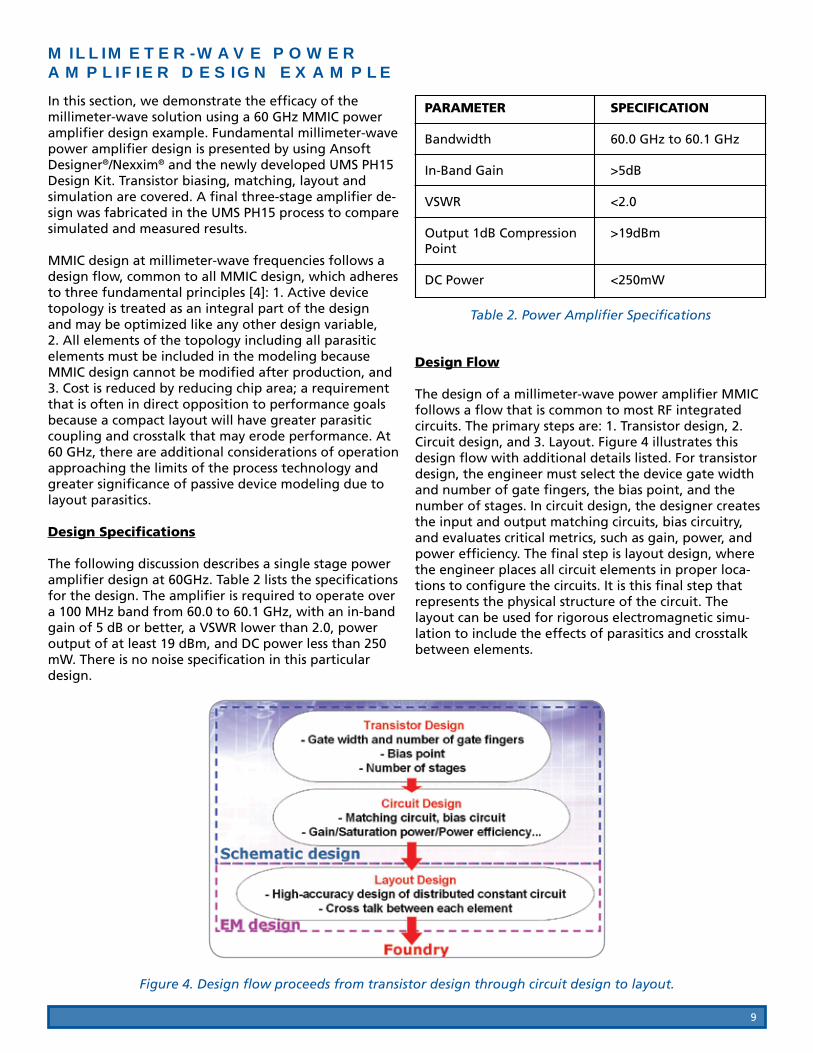
MILLIMETER-WAVE POWER AMPLIFIER DESIGN EXAMPLE
In this section, we demonstrate the efficacy of the millimeter-wave solution using a 60 GHz MMIC power amplifier design example. Fundamental millimeter-wave power amplifier design is presented by using Ansoft Designer®/Nexxim® and the newly developed UMS PH15 Design Kit. Transistor biasing, matching, layout and simulation are covered. A final three-stage amplifier de-sign was fabricated in the UMS PH15 process to compare simulated and measured results.
MMIC design at millimeter-wave frequencies follows a design flow, common to all MMIC design, which adheres to three fundamental principles [4]: 1. Active device topology is treated as an integral part of the design and may be optimized like any other design variable, �. All elements of the topology including all parasitic elements must be included in the modeling because MMIC design cannot be modified after production, and 3. Cost is reduced by reducing chip area; a requirement that is often in direct opposition to performance goals because a compact layout will have greater parasitic coupling and crosstalk that may erode performance. At 60 GHz, there are additional considerations of operation approaching the limits of the process technology and greater significance of passive device modeling due to layout parasitics.
Design Specifications
The following discussion describes a single stage power amplifier design at 60GHz. Table � lists the specifications for the design. The amplifier is required to operate over a 100 MHz band from 60.0 to 60.1 GHz, with an in-band gain of 5 dB or better, a VSWR lower than �.0, power output of at least 19 dBm, and DC power less than �50 mW. There is no noise specification in this particular design.
PARAMETER SPECIFICATION
Bandwidth 60.0 GHz to 60.1 GHz
In-Band Gain >5dB
VSWR <�.0
Output 1dB Compression >19dBm Point
DC Power <�50mW
Table 2. Power Amplifier Specifications
Design Flow
The design of a millimeter-wave power amplifier MMIC follows a flow that is common to most RF integrated circuits. The primary steps are: 1. Transistor design, �. Circuit design, and 3. Layout. Figure 4 illustrates this design flow with additional details listed. For transistor design, the engineer must select the device gate width and number of gate fingers, the bias point, and the number of stages. In circuit design, the designer creates the input and output matching circuits, bias circuitry, and evaluates critical metrics, such as gain, power, and power efficiency. The final step is layout design, where the engineer places all circuit elements in proper loca-tions to configure the circuits. It is this final step that represents the physical structure of the circuit. The layout can be used for rigorous electromagnetic simu-lation to include the effects of parasitics and crosstalk between elements.
Figure 4. Design flow proceeds from transistor design through circuit design to layout.

10
Transistor Design
As mentioned above, active device parameters are treated as continuous variables of the design in the same manner as passive elements; hence, the circuit designer is also the device designer. Most foundries provide basic transistor building blocks as part of their design rules, including gate finger length and width plus source and drain contacts. For this power amplifier application, the designer must select the width of the gate fingers, the number of fingers, and the bias point.
Figure 5 depicts the schematic used for device design as modeled in Ansoft Designer®. The pHEMT is a parameterized element in the UMS PH15 design kit. This device is placed in the schematic along with biasing chokes and voltage sources allowing sweeps of the drain voltage Vdd and the gate voltage Vg to trace curves of drain current Id, maximum gain Gmax and stability factor K versus number of fingers N and gate width Wu. Linear network analysis and DC analysis was performed using Nexxim® circuit simulator to establish the performance of the active device; a sampling of results is shown in Figure 6.
Figure 5. Schematic for device design.
(a) (b) (c)
Figure 6. Curve trace results for the circuit of Figure 5. (a) Gain and stability versus frequency forvarious number of fingers N. (b) Gain and stability versus frequency for various gate widths Wu.
(c) Drain current versus drain voltage and gate voltages.
11
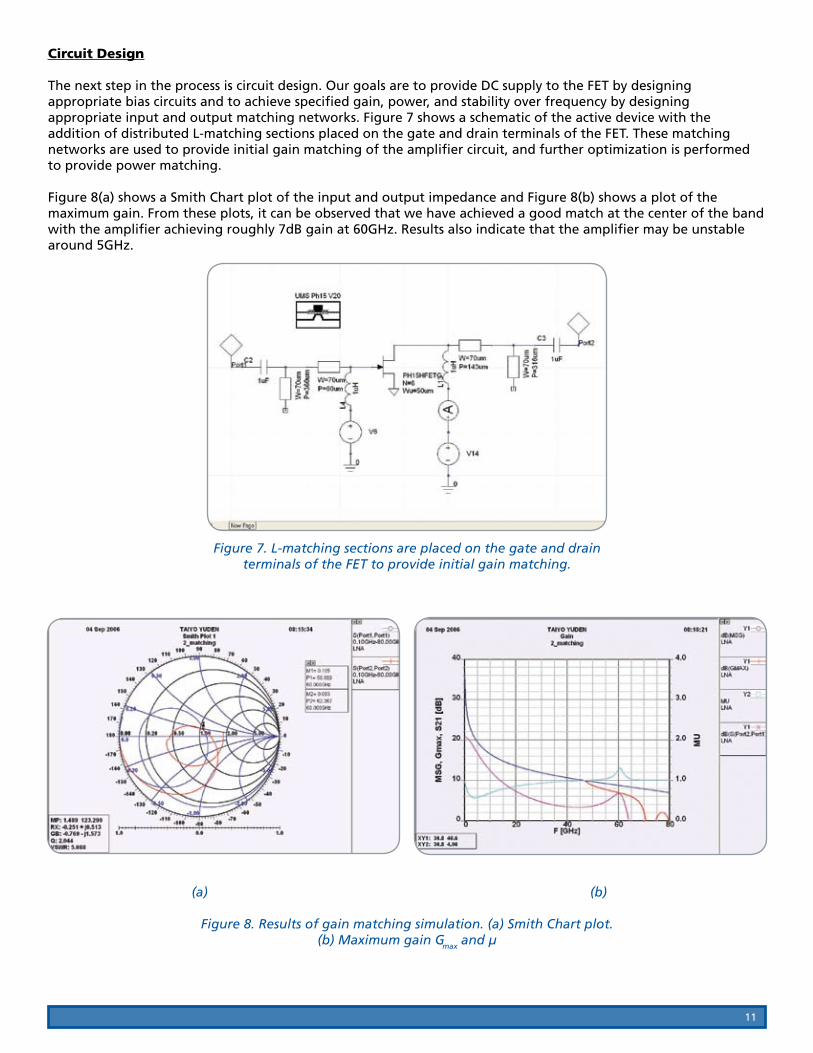
Circuit Design
The next step in the process is circuit design. Our goals are to provide DC supply to the FET by designing appropriate bias circuits and to achieve specified gain, power, and stability over frequency by designing appropriate input and output matching networks. Figure 7 shows a schematic of the active device with the addition of distributed L-matching sections placed on the gate and drain terminals of the FET. These matching networks are used to provide initial gain matching of the amplifier circuit, and further optimization is performed to provide power matching.
Figure 8(a) shows a Smith Chart plot of the input and output impedance and Figure 8(b) shows a plot of the maximum gain. From these plots, it can be observed that we have achieved a good match at the center of the band with the amplifier achieving roughly 7dB gain at 60GHz. Results also indicate that the amplifier may be unstable around 5GHz.
Figure 7. L-matching sections are placed on the gate and drain terminals of the FET to provide initial gain matching.
(a) (b)
Figure 8. Results of gain matching simulation. (a) Smith Chart plot.(b) Maximum gain Gmax and µ

1�
We now design the bias circuit and replace ideal components with actual elements from the design kit. Small adjustments in the element parameters are required in order to maintain performance. We have employed quarter wavelength, high impedance open circuited lines as a basis of the bias circuit. Capacitance values must be selected carefully to stabilize the circuit out-of-band, especially at lower frequencies. Actual elements from the PH15 Design kit were used since the bias circuit greatly affects the size of the die and the stability and circuit.
Figure 9 shows the amplifier schematic with the addition of matching and bias networks and Figure 10 shows the simulation results. This amplifier is stable across the band and achieves at least 6dB gain at 60GHz.
Figure 9. Amplifier schematic with the addition of matching and bias networks.
(a) (b)
Figure 10. Simulation results of bias circuit design. (a) Smith Chart plot.(b) Maximum gain Gmax and µ.

13
Layout
Ansoft Designer® has an integrated schematic and layout tool that allows designers to create circuits in either environment. All elements in the design kit are defined in a single database having a schematic symbol representation and an associated layout footprint representation. Because of this architecture, designers can automatically generate layout from the schematic using an automated utility. That layout can then be altered by the designer for full custom placement of elements and blocks. Figure 11 is the layout of the power amplifier automatically generated from the schematic of Figure 9. As can be seen in the figure, significant die area is consumed because the bias networks were placed far away from the FET and matching networks. Additionally, the interface to the input and output ports have abrupt changes in line width and no provision for connection between the open-ended stubs and the series matching transmission lines has been made. Nevertheless, this layout view was created with a single button click and provides valuable insight to the designer for final arrangement of the various circuit elements.
Figure 11. Layout automatically generated from the schematic of Error! Reference source not found..
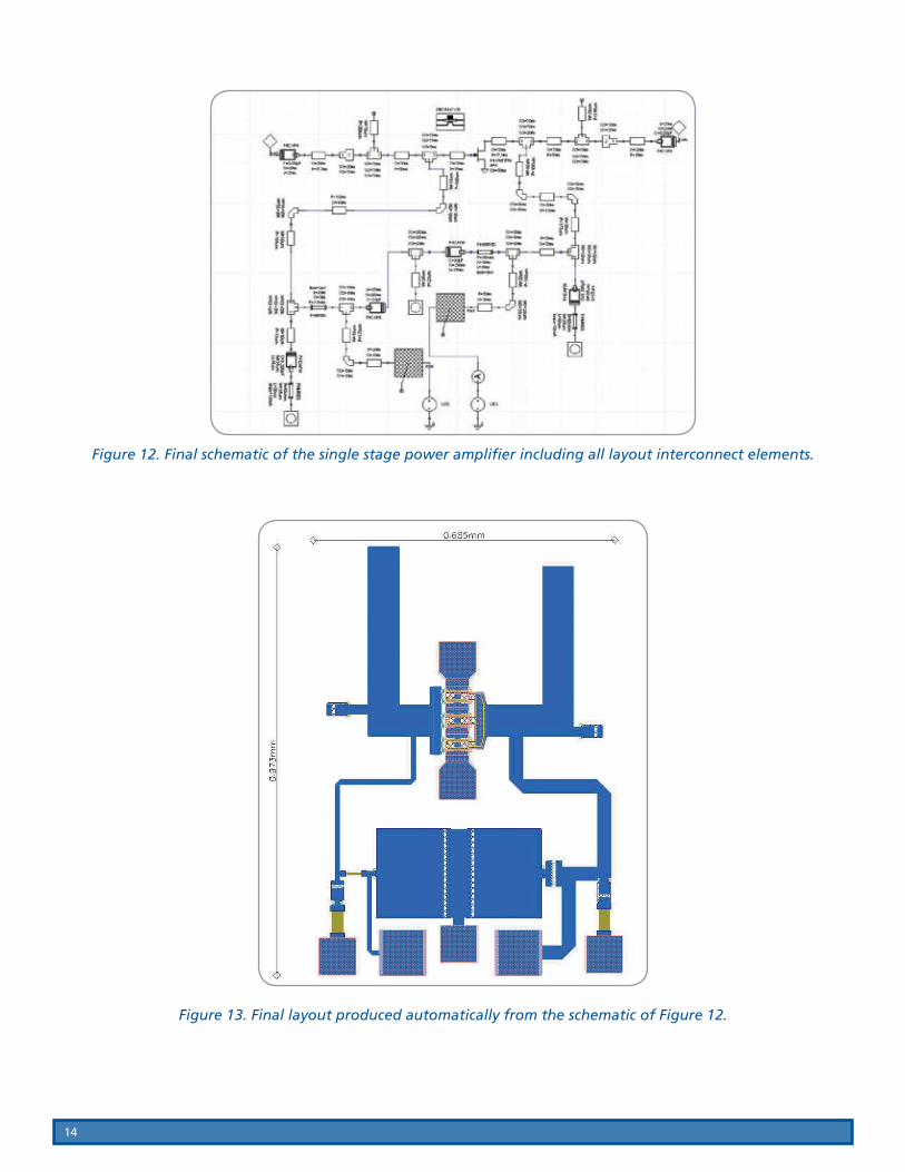
To complete the layout design, a modified schematic was created to include all transitions required for logical connection of transmission lines and to reduce the die area. Figure 1� depicts the final schematic including the additional circuit elements. Additional sections of transmission line have been added at the input and output ports along with tapered transmission line sections to make the transition from the port transmission line width to the matching network
transmission line width. A microstrip tee was added to both matching networks to allow proper connection to the open-ended stubs. Additional tee elements were added to provide connectivity to the bias network high impedance lines, which, themselves, have been further modified with chamfered 90-degree bends and additional tee elements to minimize die area as shown in the schematic. The final layout automatically generated from schematic is shown in Figure 13.
14
Figure 12. Final schematic of the single stage power amplifier including all layout interconnect elements.
Figure 13. Final layout produced automatically from the schematic of Figure 12.

15
Final Simulation Results
Complete characterization of the power amplifier with power matching requires characterization of particular power-related results, such as saturation power, P1dB, and efficiency. Harmonic balance nonlinear simulation was used to analyze such power characteristics. Traditional harmonic balance simulators were not powerful enough to characterize deep saturation ranges because those tools could only handle 5~6 harmonics. Accurately predicting circuit performance near saturation requires that a large number of harmonics are included in the simulation. Ansoft’s Nexxim® simulator enabled us to characterize the circuit with much higher harmonics and computational speed.
After completing the power match and layout with the previously described methods, the tuning capability in Ansoft Designer® may be used to adjust the element values slightly to improve performance. The result of this tuning is shown in Figure 14. The final performance of the circuit achieves linear gain of 5.3dBm P1dB of �0dBm, and drain current Idd of 7�mA at 1dB gain compression. This performance satisfies the required specifications.
Results of Experimental Fabrication
A three-stage version of the power amplifier was designed, fabricated, and measured to allow validation of the design kit and design method. The design flow described earlier was followed to choose FET size and bias points. Input and output matching circuits were designed by balancing gain, efficiency, and saturation power. Low frequency stability was achieved by distributing several picofarad capacitors across the schematic. Open stubs were used for the matching networks. The entire layout of the amplifier was simulated using Planar EM simulator and HFSS to ensure that the coupling between elements is minimized. The final circuit has a die size of �.�mm by �.8 mm, as shown in Figure 15 and Figure 16.
(a) (b)
Figure 14. Results of final circuit simulation. (a) Smith chart plot. (b) Input-output characteristics at 60 GHz.
Figure 15. Circuit schematic of thethree-stage power amplifier.
Figure 16. MMIC layout of thethree-stage power amplifier.
16
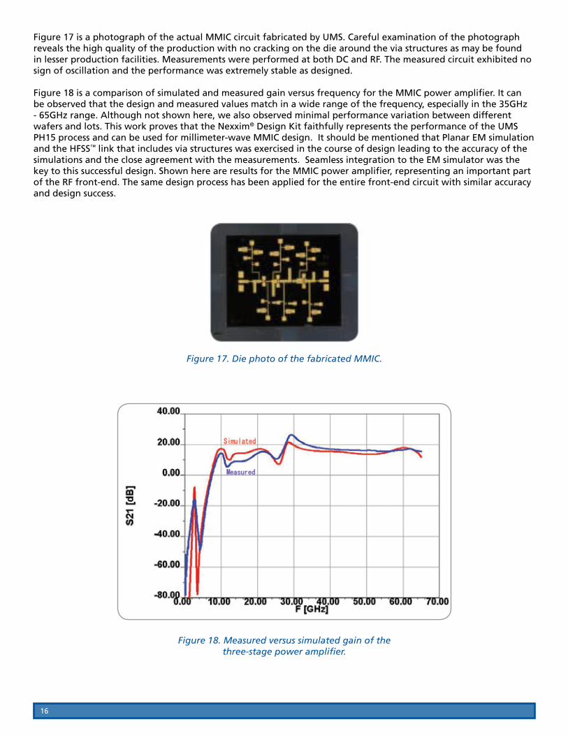
Figure 17 is a photograph of the actual MMIC circuit fabricated by UMS. Careful examination of the photograph reveals the high quality of the production with no cracking on the die around the via structures as may be found in lesser production facilities. Measurements were performed at both DC and RF. The measured circuit exhibited no sign of oscillation and the performance was extremely stable as designed.
Figure 18 is a comparison of simulated and measured gain versus frequency for the MMIC power amplifier. It can be observed that the design and measured values match in a wide range of the frequency, especially in the 35GHz - 65GHz range. Although not shown here, we also observed minimal performance variation between different wafers and lots. This work proves that the Nexxim® Design Kit faithfully represents the performance of the UMS PH15 process and can be used for millimeter-wave MMIC design. It should be mentioned that Planar EM simulation and the HFSS™ link that includes via structures was exercised in the course of design leading to the accuracy of the simulations and the close agreement with the measurements. Seamless integration to the EM simulator was the key to this successful design. Shown here are results for the MMIC power amplifier, representing an important part of the RF front-end. The same design process has been applied for the entire front-end circuit with similar accuracy and design success.
Figure 17. Die photo of the fabricated MMIC.
Figure 18. Measured versus simulated gain of thethree-stage power amplifier.

17
CONCLUSION
Taiyo Yuden, UMS, and Ansoft Corporation have teamed to meet the challenges associated with designing integrated circuits at millimeter-wave frequencies. Taiyo Yuden’s 60 GHz integrated transceiver project was the impetus for this work. They found that the high frequencies involved required new simulation technology and an advanced semiconductor process to reliably design millimeter-wave MMIC circuits. To meet these challenges, Taiyo Yuden chose circuit and electromagnetic field simulation tools from Ansoft and the UMS pHEMT PH15 GaAs MMIC process. This document described the technologies used to design millimeter-wave MMIC circuits. Rigorous device modeling and validation resulted in a millimeter-wave qualified design kit that was used in conjunction with the Nexxim® advanced circuit simulator to design a 60 GHz power amplifier. Development of this solution is valuable for emerging applications of millimeter-waves for very high-speed networking, digital communications, collision avoidance radar, and automatic cruise control systems, all of which benefit from the lower-cost solution that integration provides. The 60 GHz frequency was the primary challenge driving the technologies in this work. However, readers should recognize that additional precision, capacity, and reliability are key enablers at any frequency; hence, the design methods described here can be utilized for added fidelity and design success in microwave applications.

18
Design Kit AvailabilityThe UMS PH15 Design Kit for Ansoft Designer®/Nexxim® is available to qualified customers under non-disclosure agreement (NDA) from UMS or Ansoft and distributed by UMS. Ansoft Designer, Nexxim, and HFSS™ operate on all popular hardware plat-forms, including Microsoft Windows®, UNIX®, and Linux. Contact your UMS or Ansoft sales representative for more information.
Appendix: Design Kit InstallationDesign Kit InstallationThe design kit is provided in a .zip archive file; it can be installed by following these steps:
1. Unzip UMS PH15 DK_vX.XX (X.XX is the version number). �. Copy the UMS design kit to your Ansoft Designer3 Userlib installation directory <Designer3 Installation Directory/ Userlib/ums/ph15>. 3. Copy ph15.dll to your Model Library installation directory <Nexxim3 Installation Directory/Model_libraries>.
Figure 19. Installing UMS PH15 Design Kit.
Design Kit ConfigurationThe libraries must be configured before use. Configuration will make the contents of the library available in Ansoft Designer’s namespace. To configure the libraries, follow these steps:
1. To configure libraries for UMS Library, make sure that design’s editor window is active, and then click Configure libraries on the Tools menu.�. The Configure Design Libraries dialog box opens.3. Select the User Libraries radio button and verify that the Components library entry is selected. Scroll down the Available Libraries list and select UMS. Click the Insert button.4. Select the Symbols library entry. Select UMS from the Available Libraries menu.5. Click the Insert button and then click OK. 6. Select the Footprints library entry. Select UMS from the Available Libraries menu.7. Click the Insert button and then click OK.8. In the Components tab of the Project Manager, confirm that the UMS folder has been configured and is available for use in the design (see Figure 1).
Figure 20. Design kit configuration.References[1] J. Powell and D. Bannister, “Business prospects for commercial mm-wave MMICs,” IEEE Microwave Magazine, pp. 34 – 43, December �005.
[�] C.H. Doan, S Emami, D.A. Sobel, A.M. Niknejad, and R.W. Brodersen, “Design considerations for 60 GHz CMOS radios,” IEEE Communications Magazine, pp. 13� – 140, December �004.
[3] X. Guan, H. Hashemi, and A. Hajimiri, “A fully integrated �4-GHz eight-element phased-array receiver in silicon,” IEEETransactions on Solid State Circuits, vol. �9, no. 1�, pp. �311 – �3�0, December �004.
[4] A. Sweet, MIC & MMIC Amplifier and Oscillator Circuit Design, Artech House, 1990, pp. 139.

19
ABOUT THE COMPANIES
TAIYO YUDENNow in its 56 year, Tokyo-based Taiyo Yuden Co., Ltd. is a worldwide manufacturer of surface mount and leaded passive components, power electronics modules and wireless modules. With approximately 50% of the worldwide market in high-frequency multilayer chip inductors used in cellular phone applications, Taiyo Yuden reports annual sales of nearly US$�B. Worldwide, Taiyo Yuden employs more than seventeen thousand people, and the company’s North American affiliate, Taiyo Yuden (U.S.A.), Inc., operates sales and engineering offices in Chicago, San Jose and San Diego County. To learn more, please visit www.ty-top.com.
UMSUnited Monolithic Semiconductors designs, produces and markets leading-edge RF, microwave and millimeter-wave components and systems for the Telecom, Space, Defense, Automotive and ISM Industries. As an independent joint venture between two of the world’s leading enterprises, THALES and EADS, UMS offers a broad range of standard and custom-designed MMICs, along with an open advanced GaAs technology foundry service. The open foundry provides an integrated suite of services and high-volume capacity aimed at ensuring that ASIC designs with leading-edge performance are fabricated successfully on the first fabrication run. UMS has two production facilities, at Ulm in Germany, and Orsay in France, where the commercial headquarters and product design and development also are based. To learn more, please visit www.ums-gaas.com.
ANSOFT CORPORATIONAnsoft is a leading developer of high-performance electronic design automation (EDA) software. Engineers use Ansoft’s software to design state-of-the-art electronic products, such as cellular phones, Internet-access devices, broadband networking components and systems, integrated circuits (ICs), printed circuit boards (PCBs), automotive electronic systems and power electronics. Ansoft markets its products worldwide through its own direct sales force and has comprehensive customer-support and training offices throughout North America, Asia and Europe. For more information, please visit www.ansoft.com.

Copyright © �006 Taiyo Yuden, UMS and Ansoft Corporation TPS104-0906