wideband signal acquisition via frequency-interleaved...
TRANSCRIPT

Wideband Signal Acquisition viaFrequency-Interleaved Sampling
by
Steven William Callender
A dissertation submitted in partial satisfaction of the
requirements for the degree of
Doctor of Philosophy
in
Engineering – Electrical Engineering and Computer Science
in the
Graduate Division
of the
University of California, Berkeley
Committee in charge:
Professor Ali Niknejad, ChairProfessor Borivoje NikolicProfessor Martin White
Spring 2015

Wideband Signal Acquisition viaFrequency-Interleaved Sampling
Copyright 2015by
Steven William Callender

1
Abstract
Wideband Signal Acquisition viaFrequency-Interleaved Sampling
by
Steven William Callender
Doctor of Philosophy in Engineering – Electrical Engineering and Computer Science
University of California, Berkeley
Professor Ali Niknejad, Chair
High-speed analog-to-digital converters (ADCs) are key enabling blocks for emergingwideband applications in communication, high-end instrumentation, and medical imaging.Larger signaling bandwidth improves system performance and necessitates high-speed ADCsfor accurate digitization. As an example, current state-of-the-art oscilloscopes have an acqui-sition bandwidth exceeding 60GHz with effective sample rates greater than 100GS/s. Thisplaces significant difficulty in the design of sample-and-hold (S/H) and analog-to-digital con-version circuitry that can operate at such high speeds while providing moderate resolution.As a result, the front-end of these systems are often complex, multi-chip solutions that arefabricated in expensive processes such as indium-phosphide (InP). With the increased de-mand for battery-operable, low-power systems it is desirable to have these high-performancesignal acquisition systems in a fully-integrated CMOS implementation in order to harnessthe power of scaling as dictated by Moore’s law. To achieve this, several advancements oncurrent data conversion techniques need to be made.
In this thesis, we explore the design and optimization of a frequency-interleaved ADC(FI-ADC) as an alternative to conventional high-speed ADC architectures, which are oftenheavily time-interleaved. Due to the large interleaving factor and timing sensitivity, theconventional architectures are often very power hungry and offer typical resolutions of 4bits or less. FI-ADCs, in which the input signal is divided into various frequency bandswhich are independently digitized and digitally recombined, show less susceptibility to jitter,the primary bottleneck in high-speed ADCs. System simulations have shown a potentialimprovement in SNR performance for a frequency-interleaved ADC versus a direct sampling,time-interleaved architecture.
The focus of this thesis is to provide a fundamental understanding of the operation of theFI-ADC and investigate the similarities and differences to the conventional time-interleavedADC in respect to design complexity, design challenges and overall performance.

i
To my loving family.For always being in my corner, cheering me on.

ii
Contents
Contents ii
List of Figures iii
List of Tables v
1 Introduction 11.1 Motivation . . . . . . . . . . . . . . . . . . . . . . . . . . . . . . . . . . . . . 11.2 Thesis Overview . . . . . . . . . . . . . . . . . . . . . . . . . . . . . . . . . . 3
2 Background 52.1 High-Speed ADCs - The Time-Interleaved ADC . . . . . . . . . . . . . . . . 52.2 Frequency-Interleaved ADCs . . . . . . . . . . . . . . . . . . . . . . . . . . . 92.3 Frequency Domain Sampling vs. FI-ADCs . . . . . . . . . . . . . . . . . . . 13
3 The Frequency-Interleaved ADC 143.1 Proposed FI-ADC Architecture . . . . . . . . . . . . . . . . . . . . . . . . . 143.2 FI-ADC vs. TI-ADC . . . . . . . . . . . . . . . . . . . . . . . . . . . . . . . 22
4 Design of a 50 GS/s 6-bit FI-ADC 424.1 System-Level Design . . . . . . . . . . . . . . . . . . . . . . . . . . . . . . . 424.2 AFE Circuit Design . . . . . . . . . . . . . . . . . . . . . . . . . . . . . . . . 50
5 Measurements 765.1 FI-ADC Analog Front-End . . . . . . . . . . . . . . . . . . . . . . . . . . . . 765.2 Measurement Setup . . . . . . . . . . . . . . . . . . . . . . . . . . . . . . . . 775.3 Measurement Results . . . . . . . . . . . . . . . . . . . . . . . . . . . . . . . 79
6 Conclusion 86
Bibliography 89

iii
List of Figures
1.1 ENOB vs. fin,max for published ADCs. . . . . . . . . . . . . . . . . . . . . . . . 2
2.1 Walden FOM versus Nyquist sampling rate. . . . . . . . . . . . . . . . . . . . . 52.2 (a)Time-interleaved ADC architecture (b) Sampling diagram for 4-way TI-ADC. 62.3 CML comparator. . . . . . . . . . . . . . . . . . . . . . . . . . . . . . . . . . . . 72.4 Block diagram of the hybrid filter bank. . . . . . . . . . . . . . . . . . . . . . . 92.5 FI-ADC with downconversion mixers. . . . . . . . . . . . . . . . . . . . . . . . . 102.6 Frequency-domain sampling architecture. . . . . . . . . . . . . . . . . . . . . . . 13
3.1 Proposed FI-ADC Architecture. . . . . . . . . . . . . . . . . . . . . . . . . . . . 153.2 Simplified processing for digital reconstruction. . . . . . . . . . . . . . . . . . . 153.3 Wilkinson divider chain for broadband distribution. . . . . . . . . . . . . . . . . 163.4 Harmonic folding corrupts the baseband signal. . . . . . . . . . . . . . . . . . . 173.5 Block diagram of high frequency HRM. . . . . . . . . . . . . . . . . . . . . . . . 193.6 Sampling architectures: (top) Direct-sampling and (bot) Mix-then-sample. . . . 223.7 Input noise spectrum for mix-then-sample. . . . . . . . . . . . . . . . . . . . . . 243.8 Input noise spectrum for direct-sampling. . . . . . . . . . . . . . . . . . . . . . . 243.9 ENOB vs. input frequency (linear scale) for direct-sampling. . . . . . . . . . . . 253.10 ENOB vs. input frequency (linear scale) for mix-then-sample. . . . . . . . . . . 253.11 Timing error on sampling clock translates to a voltage error proportional to the
slope of the signal. . . . . . . . . . . . . . . . . . . . . . . . . . . . . . . . . . . 273.12 Mixing of input signal and LO with phase noise. . . . . . . . . . . . . . . . . . . 293.13 Impact of φ2
n on crossover frequency. . . . . . . . . . . . . . . . . . . . . . . . . 323.14 LO phase noise power w/o close-in phase noise. . . . . . . . . . . . . . . . . . . 343.15 Block diagram of models used for system simulation. . . . . . . . . . . . . . . . 363.16 Comparision of SNR vs. fin for different values of σjitter. . . . . . . . . . . . . . 383.17 MTS SNR vs. fin with and without LO phase noise. . . . . . . . . . . . . . . . 393.18 Comparision of SNR vs. fin without LO BPF in the MTS system. . . . . . . . . 40
4.1 Processing bands for each channel. . . . . . . . . . . . . . . . . . . . . . . . . . 444.2 Proposed architecture for digital backend. . . . . . . . . . . . . . . . . . . . . . 454.3 Tradeoff between filter rolloff and oversampling ratio. . . . . . . . . . . . . . . . 46

iv
4.4 FI-ADC AFE Block Diagram. . . . . . . . . . . . . . . . . . . . . . . . . . . . . 504.5 Conventional method for harmonic rejection. . . . . . . . . . . . . . . . . . . . . 514.6 Schematic of proposed HRM. . . . . . . . . . . . . . . . . . . . . . . . . . . . . 524.7 Alternative schematic for HRM. . . . . . . . . . . . . . . . . . . . . . . . . . . . 534.8 Performance comparison of two HRM topologies. . . . . . . . . . . . . . . . . . 534.9 Schematic of HRM gm stage. . . . . . . . . . . . . . . . . . . . . . . . . . . . . . 554.10 Simulated HRR vs. rise/fall time mismatch between main and aux. mixers. . . . 564.11 HRR vs. erise as predicted by Equation 4.8. . . . . . . . . . . . . . . . . . . . . 574.12 Magnitude and phase error caused when tr,main 6= tr,aux (fLO = 4GHz). . . . . . 584.13 Schematic of Distributed Amplifier. . . . . . . . . . . . . . . . . . . . . . . . . . 594.14 Plot of RHS and LHS of Equation 4.5 for various system specifications. . . . . . 604.15 Simulated frequency response of the DA. . . . . . . . . . . . . . . . . . . . . . . 614.16 Simulated group delay response of the DA. . . . . . . . . . . . . . . . . . . . . . 614.17 DA frequency response of according to Equation 4.22. . . . . . . . . . . . . . . . 654.18 DA group delay response of according to Equations 4.21a and 4.21b. . . . . . . 664.19 Schematic of current-mode lowpass filter. . . . . . . . . . . . . . . . . . . . . . . 674.20 Equivalent circuit for current-mode lowpass filter. . . . . . . . . . . . . . . . . . 684.21 Simualted magnitude response of lowpass filter. . . . . . . . . . . . . . . . . . . 694.22 Simulated group delay response of lowpass filter. . . . . . . . . . . . . . . . . . . 694.23 Noise response lowpass filter. . . . . . . . . . . . . . . . . . . . . . . . . . . . . 704.24 Schematic of high-speed CML latch-based divider. . . . . . . . . . . . . . . . . . 714.25 Architecture used for SSB mixing. . . . . . . . . . . . . . . . . . . . . . . . . . . 724.26 Current buffer for SSB mixer. . . . . . . . . . . . . . . . . . . . . . . . . . . . . 734.27 CMOS inverter chain used for 3, 6, and 9 GHz LO buffering. . . . . . . . . . . . 744.28 Placement of intermediary buffers to reduce load transformations. . . . . . . . . 744.29 Planar twisted pair technique used for LO routing. . . . . . . . . . . . . . . . . 75
5.1 Die photo of FI-ADC AFE. . . . . . . . . . . . . . . . . . . . . . . . . . . . . . 775.2 Measurement setup. . . . . . . . . . . . . . . . . . . . . . . . . . . . . . . . . . 785.3 Generation of phase-coherent 36GHz and 48GHz input. . . . . . . . . . . . . . . 795.4 IIP2/3 measurements. . . . . . . . . . . . . . . . . . . . . . . . . . . . . . . . . 815.5 P1dB measurements. . . . . . . . . . . . . . . . . . . . . . . . . . . . . . . . . . 825.6 SNDR measurements. . . . . . . . . . . . . . . . . . . . . . . . . . . . . . . . . 825.7 FFT of baseband signal for 24.1GHz and 25.1GHz input signals. . . . . . . . . . 835.8 Spectrum of analog output. . . . . . . . . . . . . . . . . . . . . . . . . . . . . . 835.9 Impact of noise sideband on measured ENOB. . . . . . . . . . . . . . . . . . . . 845.10 Measured phase response of phase interpolator. . . . . . . . . . . . . . . . . . . 845.11 Measured phase steps of phase interpolator. . . . . . . . . . . . . . . . . . . . . 85

v
List of Tables
1.1 ADC specifications for various high-speed applications. . . . . . . . . . . . . . . 2
4.1 Pros and Cons for larger number of channels. . . . . . . . . . . . . . . . . . . . 434.2 Sub-ADC sample rate (in GS/s) vs. Filter order/type. . . . . . . . . . . . . . . 47
vi
Acknowledgments
This research would not have been possible without the guidance of my advisor, AliNiknejad. Throughout my seven years at Berkeley, Ali has provided sound advice andencouragement that helped me develop both professionally and personally. There is no needto comment on his brilliance as a researcher and lecturer – this is already well-known. Instead,I would like to thank him for his patience as an advisor. Never once did I feel pressured topush out a publication or prematurely present my results. Ali insisted on digging deeper tomake sure a fundamental understanding was obtained and to get to the root of the issue.One of my most testing moments in graduate school occured in 2013 when I missed thefirst tapeout of the FI-ADC chip after working tirelessly (14+ hour days) for 3 consecutivemonths. Feeling defeated and a bit embarassed, I had a meeting with Ali on the submissiondate to relay the bad news. Instead of responding with a tone of disappointment, Ali spokewords of encouragement that helped lift my spirits and get me back on my feet.
I would also like to thank my dissertation committee, Bora Nikolic, Elad Alon, andMartin White for overseeing my research and providing constructive feedback on points thatneeded strengthening. I would like to further thank Bora for the phone call he made on hisway home from the office, back when I was a new admit, aiming to convince me to come toBerkeley. Berkeley was already my top choice, but it was good to hear a voice expressingBerkeley’s interest in my talents. And Elad, for strengthening my circuits knowledge in theclassroom and always having an open door when I needed to discuss research.
The FI-ADC chip presented in this thesis would not have been possible if it weren’t forthe help and support of Lucas Calderin and Greg LaCaille. As first-year graduate studentswith little-to-no tapeout experience, they joined the project and took on the resposibility ofdesigning the LO generation and distribution for a tapeout that was five months away. Itwas quite impressive to see how swiftly they caught up to speed and how they quickly begancontributing to design decisions in the overall FI-ADC. It was a pleasure working alongsidethem and making the late night trips to Safeway during tapeout.
I would like to thank SRC and the TxACE program for funding the FI-ADC project. Iwould also like to thank Robert Noyce Fellowship for funding part of my graduate studies,Texas Instruments for generously donating the ADCs that were used for testing the FI-ADCfront-end, Keysight, Integrand and Ansoft for software donations. Thanks are also due tothe BWRC industrial sponsors who have provided valuable feedback on this project at oursemi-annual research retreats.
I would like to acknowledge the first group I ever worked with at Berkeley, the TUSI team:Amin Arbabian, Shinwon Kang, Jun-Chau Chien, Ali (Bagher) Afshar and Ehsan Adabi.It was an honor and privelege to work alongside such gifted and hard-working researchers.Working on the TUSI project, I learned how to effectively work in a group and collectivelytackle a large problem. Amin, the headmaster of it all, unknowingly played the role ofco-advisor in my formative years at Berkeley. He is truly a unique talent and one of thebrightest individuals I have ever worked with.

vii
I have also had the privelege to work alongside the talented individuals of Ali Niknejad’sresearch group (past and present) : Siva Thyagarajan, Jiashu Chen, Maryam (Sahar) Tabesh,Ashkan Borna, Sriramkumar Venugopalan, Pramod Murali, Lu Ye, Cristian Marcu, AndrewTownley, Nai-Chung Kuo, Nima Baniasadi, and Paul Swihurn. These individuals were aninvaluable resource throughout my graduate years, providing informative discussions anddebates on various research topics and circuits questions.
Outisde of our research group, I have made many friends and colleagues at BWRC: MilosJorgovanovic, Katerina Papadopoulou, William Biederman, Dan Yeager, Matt Weiner, MattSpencer, Rikky Muller, Simone Gambini, Yida Duan, Yue Lu, Charles Wu, Chintan Thakkar,Lingkai Kong, John Crossley, Angie Wang, Rachel Hochman, Amanda Pratt, and SharonXiao. I would like to thank them all for their friendsip and camaraderie and for makingBWRC one of the best research centers to work in.
In addition, many thanks are due to the BWRC staff (past and present): Brian Richards,Fred Burghardt, Deirdre McAuliffe-Bauer, Gary Kelson, Leslie Nishiyama, Olivia Nolan,Sarah Jordan, Bira Coelho, Susan Mellers and Tom Boot. These individuals have helpedkeep the BWRC running smoothly over the years and tended to all research needs of thestudents.
I am fortunate to have also formed lasting friendships with EECS colleagues outside ofBWRC: Michael Lorek, Henry Barrow, Bobby Schneider, Richard Przybyla and MitchellKline. We’ve shared many beers together in order to shed away the stresses of grad schoolwhich really helped me keep my sanity throughout the years.
I would also like to thank the EECS department and staff, namely, Shirely Salanio, SheilaHumphreys, Patrick Hernan, and Ruth Gjerde for making sure I properly progressed throughmy graduate studies.
Before Berkeley, there was Columbia. I would like to thank my friends who have been withme on this journey since undergrad: Brian Ramos, Carlene Liriano, Ed Liao, Josh Breslow,Jonathan Barbee, Keith Dronson, Frank Zovko, Jessica Lin, Dan Llamas, Emmanuel-SeanPeters, and David Diaz. I would also like to give a special thanks to my undergraduateresearch advisor at Columbia, Professor Yannis Tsividis, who took me under his wing as abright-eyed freshman and nourished the beginnings of my career in research.
Last, but certainly not least, I would like to thank my entire family. I would not be whereI am today if it were not for the love and support of my mother, Marcia Simms. She hasbeen my number one supporter since day one. Words cannot express how indebted I am toher. I am also indebted to my father, Alfred (Billy) Callender for providing constant wordsof wisdom throughout the years. He has always emphasized the value of education and workethic from when I was young. I would like to thank him for never settling for my 98% testscores and always questioning (half-jokingly) why I did not get a 100%. My #2 fans wouldhave to be my beautiful sisters, Stephanie Callender and Raynelle Callender-McKissick.Thank you for always looking after your “little bro” and showing me unconditional love.And to my large, beautiful, and loving family – aunties, uncles, cousins, and in-laws – thankyou for everything you have given me. You all are the village that raised me.

1
Chapter 1
Introduction
There is an ever-increasing demand for higher bandwidth systems. Modern day high-speed serial links, oscilloscopes, and pulsed mm-wave imagers have illustrated a need foranalog-to-digital converters with sample rates exceeding 50GS/s and resolutions greater than6 bits. These are extremely difficult specifications to meet using current approaches and thesystems that do meet these specifications are often wall-powered and done in non-CMOSprocesses. In this thesis, we explore an alternative approach to high-speed analog-to-digitalconversion that can provide improved resolutions at very high input frequencies with lowpower consumption in current-day CMOS technologies.
1.1 Motivation
High-speed analog-to-digital converters (ADCs) have traditionally been utilized in veryniche applications (e.g. high-end oscilloscopes). With the increased speed offered by deeplyscaled CMOS processes and the increased demand for communication data rates, high-speedADCs have found more frequent usage in both traditional and emerging applications. Therequired specifications of these high-speed ADCs depends on application. Table 1.1 showssample numbers for the required sample rate (SR) and effective number of bits (ENOB) ofADCs used in various applications.
For cellular LTE technology, the maximum sample rate is 200−250MS/s which is consid-ered high-speed for common consumer applications. The resolution of these ADCs is quitehigh, which is why ∆Σ ADCs are very popular for cellular receivers [1]. In contrast, mm-wave imaging for medical applicatons, an emerging application, requires sample rates twoorders of magnitude higher than what is required for cellular applications but scales back onthe necessary resolution. This application is of particular interest since it is the root projectfrom which this work developed.
As discussed in [2], pulsed mm-wave imagers can be utilized in a myriad of applicationssuch as medical diagnosis and gesture recognition. For these applications, transmission ofnarrow pulses is desirable since there is an inverse relationship between the pulse width and

CHAPTER 1. INTRODUCTION 2
the depth resolution of the imager. In the case of medical diagnosis,
Cellular HS Links HS OScopes UWB Imaging (TUSI)Fs [GHz] 0.25 5-20 160 20-50
ENOB [bits] 9-10 3-6 8 6
Table 1.1: ADC specifications for various high-speed applications.
narrower pulses improve depth resolution and can lead to earlier detection of cancerous cells.In [3] and [4], 94GHz transceivers were designed for usage in a Time-domain Ultra-widebandSilicon Imager (TUSI) system. [3] demonstrated a 94GHz transmitter that was capable oftransmitting record pulse widths down to 26ps. In [4], a similar transmitter was paired witha receiver to demonstrate the transmission and detection of pulses down to 30ps. Using aquadrature receiver, this translates to baseband bandwidths on the order of 20GHz. Thereceiver in that design was composed of a wieband LNA and downconverting micro-mixers,omitting the baseband digital processing. The reason for this was the inexistence of ADCtechniques that could meet the required the specifications (20 − 50GS/s, fin,max > 25GHz,and 6b ENOB). This is still the case as can be seen from Figure 1.1 which plots the ENOBof published ADCs as a function of the maximum input frequency.
Figure 1.1: ENOB vs. fin,max for published ADCs.

CHAPTER 1. INTRODUCTION 3
From the above plot, it is seen that the ENOB begins to continuously decrease as theinput frequency is increased above 100MS/s. This region is referred to here as the jitter-limited regime. In this region, the attainable ENOB of the ADC is no longer determinedby the quantization noise, but is instead limited by the aperture jitter - timing errors onthe sampling clock lead to voltage errors in the digital representation. Because of this issue,the majority of ADCs sampling above 20GS/s have ENOBs less than 5b. As can be seenin the plot, in order to have a chance at obtaining ENOBs greater than 6b for frequenciesabove 20GHz, the sampling clock must have an rms-jitter less than 100fs-rms which is achallenging task. As a result, it is worth exploring techniques that can potentially break thejitter-barrier faced by current ADC architectures.
Why Frequency-Interleaved?
The frequency-interleaved ADC (FI-ADC) is an alternative approach to high-speed dataconversion [5]. It has the attractive quality that it is less sensitive to sampling jitter and canpotentially improve the attainable resolution of high-speed ADCs given the same amountof rms-jitter. It accomplishes this by channelizing the input into various frequency sub-bands thereby limiting the maximum signal frequency presented to the sampler. Althoughthere are other cited benefits of the FI-ADC [5], the decreased sensitivity to jitter is themost important feature when it comes to high-speed data conversion. As such, this thesisaims to provide a proper understanding of how the FI-ADC can (potentially) achieve higherresolution over the conventional architectures. This thesis also aims to help develop insightinto how to properly design an FI-ADC system in order to reduce system complexity andpower consumption.
1.2 Thesis Overview
This thesis is organized as follows:Chapter 2 provides a background on the dominant high-speed ADC architecture, the
time-interleaved ADC (TI-ADC). Operation of the TI-ADC is first discussed, followed bydesign challenges and performance limitations. The FI-ADC, as proposed by [5], is thenintroduced followed by a review of several FI-ADC designs.
Chapter 3 presents the proposed FI-ADC architecture that is used in this project. A dis-cussion of the key design challenges such as wideband signal distribution, harmonic folding,LO generation and digital reconstruction is provided. Next, a detailed comparison betweenthe FI-ADC and TI-ADC is presented. The heart of this section is found in the discussionof the impact of LO phase noise on FI-ADC performance. Until now, there as been littleto no discussion on how LO phase noise impacts the overall performance of FI-ADCs. Thischapter concludes with a summarization of system-level simulations which were performedto compare the two architectures.

CHAPTER 1. INTRODUCTION 4
Chapter 4 provides a guideline to the design of a 50GS/s 6-bit FI-ADC. System-leveldesign considerations are discussed. The design of the FI-ADC analog front-end (AFE)which was taped out and measured is then presented. Chapter 5 reports the measurementresults of the taped out chip.
Chapter 6 summarizes and concludes the thesis.

5
Chapter 2
Background
2.1 High-Speed ADCs - The Time-Interleaved ADC
The time-interleaved (TI) ADC [6] is the most commonly used architecture for high-speedADCs, especially for designs aiming to achieve the highest sample rate in a given process.This can be seen in Figure 2.1 which plots the Walden figure-of-merit, FOMW , versus theNyquist sampling rate for all ADCs published in ISSCC and VLSI [7][8].
Figure 2.1: Walden FOM versus Nyquist sampling rate.

CHAPTER 2. BACKGROUND 6
The TI-ADCs are circled in red and dominate the right-hand side of the plot (fs,nyq >1GHz). The reason for its dominance at these high frequencies is that the TI-ADC enablesmore energy-efficient designs than the flash ADC, another popular architecture for high-speed ADCs. The ability to realize energy-efficient designs becomes apparent after lookingat the architecture and operation of the TI-ADC.
A block diagram of the TI architecture is shown in Figure 2.2(a). It is comprised of Msub-ADCs working in parallel, each sampling the input signal at 1
Mth the full sample rate
(i.e. φ1...M are clocks of frequency fsM
). The phases of the sampling clocks for each channel(φ1...M) are equi-spaced across the full sample period (Figure 2.2(b)). The outputs of eachchannel are time-multiplexed into a single stream at the output that represents the samplesof the input signal at the full sample rate, fs.
Figure 2.2: (a)Time-interleaved ADC architecture (b) Sampling diagram for 4-way TI-ADC.
Since each sub-ADC is operating at a fraction of the full sample rate, more energy-efficient designs can be used. This is because the sub-ADC has a longer period to performthe sample-and-hold and comparison operations, which can be very power hungry when verysmall conversion times are required. Take the CML comparator for example. It is comprisedof a gain stage followed by a regenerative latch (Figure 2.3). The combined amplificationtime, tamp, and regeneration time, tregen must be less than the clock period. tregen is typicallythe bottleneck of the two, and is given by[9]:
tregen = ln(Alatch) ·CLgm
(2.1)
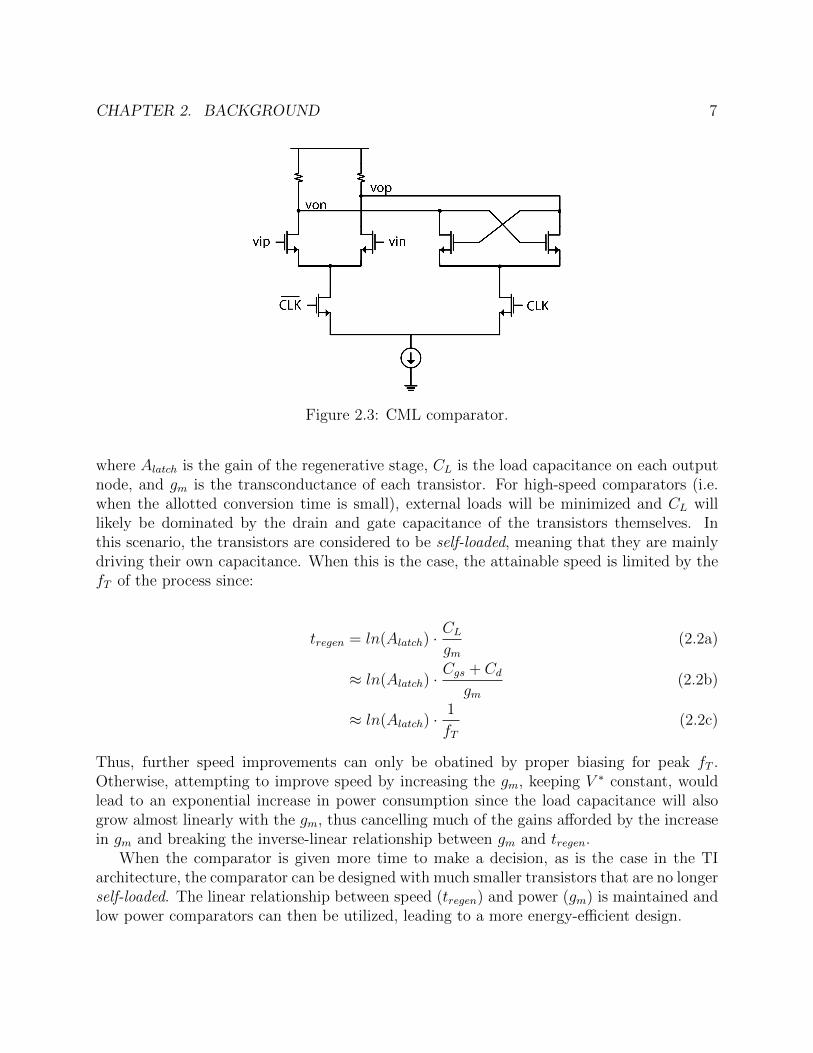
CHAPTER 2. BACKGROUND 7
Figure 2.3: CML comparator.
where Alatch is the gain of the regenerative stage, CL is the load capacitance on each outputnode, and gm is the transconductance of each transistor. For high-speed comparators (i.e.when the allotted conversion time is small), external loads will be minimized and CL willlikely be dominated by the drain and gate capacitance of the transistors themselves. Inthis scenario, the transistors are considered to be self-loaded, meaning that they are mainlydriving their own capacitance. When this is the case, the attainable speed is limited by thefT of the process since:
tregen = ln(Alatch) ·CLgm
(2.2a)
≈ ln(Alatch) ·Cgs + Cd
gm(2.2b)
≈ ln(Alatch) ·1
fT(2.2c)
Thus, further speed improvements can only be obatined by proper biasing for peak fT .Otherwise, attempting to improve speed by increasing the gm, keeping V ∗ constant, wouldlead to an exponential increase in power consumption since the load capacitance will alsogrow almost linearly with the gm, thus cancelling much of the gains afforded by the increasein gm and breaking the inverse-linear relationship between gm and tregen.
When the comparator is given more time to make a decision, as is the case in the TIarchitecture, the comparator can be designed with much smaller transistors that are no longerself-loaded. The linear relationship between speed (tregen) and power (gm) is maintained andlow power comparators can then be utilized, leading to a more energy-efficient design.

CHAPTER 2. BACKGROUND 8
TI-ADC Designs and Challenges
Input Buffer
There has been significant progress over the past several years in improving the energy-efficiency and speed of TI-ADCs. Recently, a TI-ADC capable of sampling at rates up to90GS/s was presented [10]. Designed in a 32nm SOI process, one of the key merits of thisdesign was the sampling circuitry and clock generation which are critical for time-interleaveddesigns and can consume a significant fraction of the overall power. Although, the Nyqusitfrequency is 45GHz at this sample rate, the acqusition bandwidth of the converter waslimited to 20GHz. This is likely due to the limited bandwidth of the input buffer, the detailsof which was omitted by the authors. Nevertheless, the input buffer design is generallya huge bottleneck in TI-ADC designs with a large number of channels due to large inputcapacitance. As a result, the input buffers can ultimately limit the acquisition bandwidth ofthe converter and/or consume a lot of power1.
Channel Mismatch and Calibration
Another design challenge for TI-ADCs is the effect of channel mismatch. Ideally, allchannels should have an identical response to the input signal so that when their outputstreams are combined, it appears as if the input was sampled by a single-channel ADC.Unfortunately, there is always mismatch amongst the channel in the form of gain, offset,clock skew, and bandwidth. The presence of these types of mismatch leads to distortion tonesto appear in the output spectrum, ultimately limiting the attainable SNDR [11].
There has been extensive work done on mitigating the effects of mismatch via calibra-tion. [12] and [13] illustrate some of the modern calibration techniques, such as derivativeestimation, and achieve 8b ENOB for speeds of 2.8 and 1.6GS/s, resepctively.
Clock Jitter
As mentioned in Chapter 1, the majority of high-speed ADCs operate in the jitter-limitedregime. In this region of operation, the attainable ENOB is no longer limited by thermalnoise or distortion, but is instead limited by the aperture error caused by jitter on thesampling clock. Timing errors in the sampling instant result in voltage errors in the sampledsignal (Chapter 3) which degrade the overall SNR of the sampled signal. The theoreticallyattainable SNR in the presence of rms clock jitter, σj, is given by:
SNRj = −20log(2πfinσj) (2.3)
According to Equation 2.3, in oder to achieve 25 GHz of acquisiton bandwidth and atleast 6b of resolution, the front-end sampler needs to be driven by a (50GHz) clock withless than 80fs of rms-jitter, which is extremely difficult to obtain from an integrated source.
1The power consumption of the input buffer in [10] was not included in the reported power number.
CHAPTER 2. BACKGROUND 9
Current state-of-the-art frequency synthesizers at similar frequencies achieve rms-jitter valueson the order of 200-300fs [14][15]. This is why almost all high-speed ADC publications usean external clock source for testing.
For some high-speed applications (e.g. frequency-domain channel equalization), 4-5bresolution ADCs are sufficient to meet the system specifications and the TI architecturecan be used. However, there are both current and emerging applications, such as real-timewideband signal capture (oscilloscopes) and mm-wave imaging, that require resolutions inthe range of 6-8b which cannot be done without a very clean clock source and, in turn, alot of power. Thus, it of interest to explore alternative topologies that can potentially relaxthe sensitivity of the ADC system to the clock jitter and improve the attainable SNR ofhigh-speed ADCs. One potential candidate is the frequency-interleaved ADC.
2.2 Frequency-Interleaved ADCs
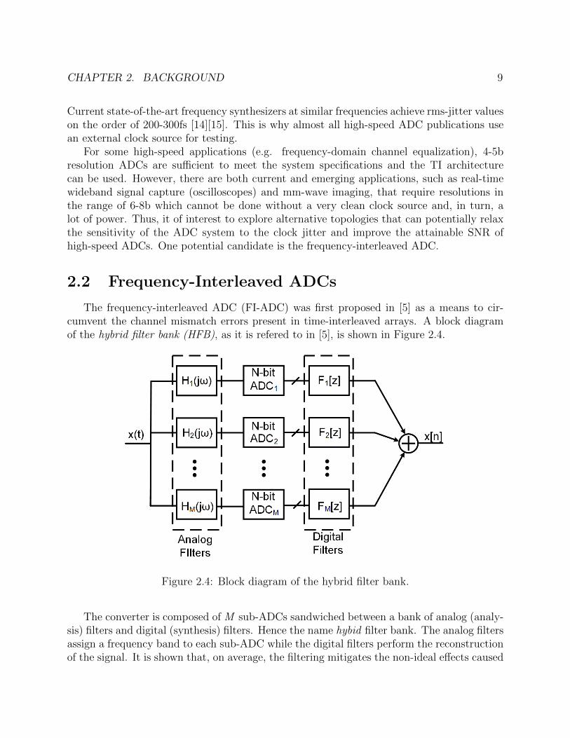
The frequency-interleaved ADC (FI-ADC) was first proposed in [5] as a means to cir-cumvent the channel mismatch errors present in time-interleaved arrays. A block diagramof the hybrid filter bank (HFB), as it is refered to in [5], is shown in Figure 2.4.
Figure 2.4: Block diagram of the hybrid filter bank.
The converter is composed of M sub-ADCs sandwiched between a bank of analog (analy-sis) filters and digital (synthesis) filters. Hence the name hybid filter bank. The analog filtersassign a frequency band to each sub-ADC while the digital filters perform the reconstructionof the signal. It is shown that, on average, the filtering mitigates the non-ideal effects caused

CHAPTER 2. BACKGROUND 10
by gain and phase mismatch between the channels. This is because a single-tone signal willideally be processed by a single channel, whereas in the TI case, the output samples fora single-tone signal are taken from all channels, allowing the mismatch errors to compiletogether. The worst-case performance occurs in the transition band between channels sincea single-tone in that band will be simultaneously processed by two channels.
Although the architecture and analysis presented in [5] focused on mitigating channelmismatch effects, the author briefly mentions the potential for reduced jitter sensitivity dueto the reduced bandwidth presented to the sampler. Many works have since focused onapplying this idea to various applications in order to take advantage of both the channelmismatch and jitter sensitivity benefits [16][17][18][19][20][21].
In [16], the authors used a three-channel frequency-intereaved (channelized) architec-ture for a 12.5GS/s serial link. Although the resolution is relatively low (3b), the authorswere aiming to improve upon the performance of high-speed digitizers available at the time,citing jitter sensitivity and channel mismatch as the major bottlenecks for TI converters.Interestingly enough, the authors further interleaved the sub-ADCs using a 2-way TI-ADCarchtiecture in order to further relax the sampling speed requirements of each ADC. Inthat design, the top-level frequency-interleaved architecture enables higher resolutions tobe achieved via reduced jitter sensitivity, while the low-level time-interleaved architectureallows for energy-efficient sub-ADCs to be utilized. Lastly, I/Q downcoversion mixers areused in each passband channel in order to translate each frequency band down to basebandbefore sampling and reduce the required sampling speed of each sub-ADC (Figure 2.5). Thisdownconversion was not needed in [5] due to the low overall sampling speed.
Figure 2.5: FI-ADC with downconversion mixers.

CHAPTER 2. BACKGROUND 11
In [18], a two and three-channel FI architecture is used to design a 4 and 6GS/s ADCwith 4b resolution in 90nm CMOS. The design integrates the full mixer-filter-ADC path.Reconstruction of the input signal is done offline and incorporates digital correction of gainand phase mismatches in the I/Q paths and gain/offset mismatches across the channels.A more detailed discussion of the digital compensation techniques are discussed in [22].Measurements show a peak ENOB of 3.5b and futher demonstrate how a moderate ENOBis maintained over the entire Nyqust band (less than 1b degradation). This relatively flatENOB response is a theoretical characteristic of the FI architecture and is further discussedin Chapter 3.
At this point, it should be noted that the designs in [16] and [18] restrict the number ofchannels in the FI architecture to two or three. The benefit of this decision is that thesedesigns aren’t susceptible to the harmonic folding problem that occurs once your numberof channels is greater than three (Chapter 3). Unfortunately, as the speed of the converteris increased2, a larger number of channels becomes necessary in order to allow for energy-efficient (and feasible to implement) sub-ADCs to be used and lead to an overall energy-efficient design. As such, harmonic rejection techniques need to be employed in the design ofthese FI architectures. Additionally, the larger channel count increases the input capacitiveload and makes the distribution of the wideband signal to all channels more difficult and/orpower hungry. Techniques to address these two key problems are presented in the laterchapters.
In [19] and [20], the FI architecture is used to design wideband multi-channel receiverswith more than three channels. [19] uses a five-channel FI architecture to simulate a 5GHzbandwidth OFDM receiver. The effective sample rate of the receiver is 10GS/s with atargeted SNR of 40dB (6.35b resolution). The authors propose the usage of “bandwidth-optimized” low-order filters in the sub-channels in order to reduce power consumption anddesign complexity. According to their simulations, reducing the bandwidth of first andsecond-order filters to below the pre-allocated channel bandwidth results in significant re-duction in jitter sensitivity. This is due to the improved filtering of out-of-band signals whichwould normally reciprocally mix with the wideband phase noise of the LO and degrade thein-band noise floor. Since in-band signals are also partially attenuated in this scheme, theyrely on their reconstruction algorithm to correct for any in-band losses. Furthermore, theirsimulations show that the SNR degradation due to jitter dominates the degradation due tonoise added during mixing, which isn’t the case for the design presented in this thesis. It islikely that the aggressive filtering in each channel helps mitigate the impact of the LO phasenoise added during mixing (see Chapter 3).
While the techniques proposed in [19] are innovative and have the potential to signifi-cantly relax the design of the LOs and channel filters, they are not adopted in this design fortwo reasons: (1) Group delay variations across channels will be severe due to the purposefulin-band filtering. This may take more effort to correct in the digital domain since the band-width of the equalized channel would have to be extended further than the pre-allocated
2The target of design presented in this thesis is 50GS/s.
CHAPTER 2. BACKGROUND 12
bandwidth3. For applications requiring the reconstruction of the full wideband signal, mis-match in the group delay between channels will result in imperfect reconstruction of thesignal. (2) The corner frequency of the analog filters would need to be well controlled inorder for the digital backend to properly equalize the in-band attenuation without causingfurther distortion. This neccessitates tuning circuitry for the filter’s corner frequencies, andadds to the design complexity.
In [20], a four-channel FI architecture is used to design a 2GS/s sampling receiver in65nm CMOS. The receiver has an acquisition bandwidth of 125MHz to 1GHz and maintainsan impressive (mean) ENOB of 7.8b across the entire bandwidth and harmonic rejectiongreater than 59dB. At the time of this writing, this is one of the very few (and possiblyonly) receivers to address the haromonic folding problem that plagues the FI architecturewhen more than three channels are used. The harmonic rejection is performed in the digitalbackend via the shuffling of weighted coefficients to synthesize a sampled-and-held sinusoidwith reduced harmonic content. The coefficient shuffling is also cleverly used to change thefrequency of the effective LO, enabling programmable channel selection. The one drawbackof this architecture is that it only allows the reception of a single channel at any giventime. Although adequate for their targeted application, this is not sufficient for applicationsrequiring real-time reception of an entire broadband spectrum.
It should also be noted that the FI-ADC technique has found usage in commercial appli-cations, specifically high-speed oscilloscopes [23]. In this patent, a two-channel architectureis used to practically double the acquisition bandwidth of a real-time oscilliscope front-end.By simply highpass filtering and downconverting the upper-half of the spectrum, the samehigh-speed baseband ADC can be used. With only a two-channel architecture, harmonicfolding is not a problem for their design. Additionally, since it isn’t a power-constraineddesign (wall-powered), it isn’t an issue to re-use the very power hungry 40GS/s sub-ADC foreach channel. For low power designs, this architecture would of course have to be altered toincorporate more channels, as done in this thesis. However, it is still interesting to see thatthe FI architecture has been utilized to design modern oscilloscopes with effective samplerates of 240GS/s and resolutions of 6-8b.
The basics of digital reconstruction are also detailed in [23] and are used in the design ofthe offline digital reconstruction for the FI-ADC presented in Chapter 4.
3See Chapter 4 for further discussion.

CHAPTER 2. BACKGROUND 13
2.3 Frequency Domain Sampling vs. FI-ADCs
Frequency-domain sampling is an alternate version of the frequency-interleaving topologywhich has also been researched [21][24]. The key difference is the replacement of the LPFwith an integrator (Figure 2.6). The integrator and sampler effectively perform a DFToperation and, as a result, the reconstruction of the signal is done by performing an IFFTin the digital backend. As discussed in [21], because the DFT inherently assumes a periodicsignal, the improved ADC resolution is only achieved for frequencies that are Ti-periodic,where Ti is the length of the integration period. In order to solve this problem, a windowingfunction must be applied to the signal before sampling4. Once this window function hasbeen applied, the output signal becomes an approximation of the input signal, in the bestcase.
Figure 2.6: Frequency-domain sampling architecture.
Although the frequency-domain ADC may have merits for potential usage in multi-bandreceivers [24], it is not adopted here. For one, the approximation that is inherent in thearchitecture is not be suitale for applications requiring accurate reconstruction of the wide-band signal (e.g. oscilloscopes). Secondly, the windowing function effectively smooths outany sharp transitions/edges in the signal so that the signal could be represented by a finitenumber of DFT coefficients. This is undesirable for pulsed-radar imagers which rely on time-of-arrival (TOA) information. The TOA is encoded in the pulse edge and smoothing outthis edge can alter the measured TOA and affect the accuracy of high-resolution imagers.
4This is commonly done in DSP for DFT/FFT calculations of arbitrary waveforms.
14
Chapter 3
The Frequency-Interleaved ADC
3.1 Proposed FI-ADC Architecture
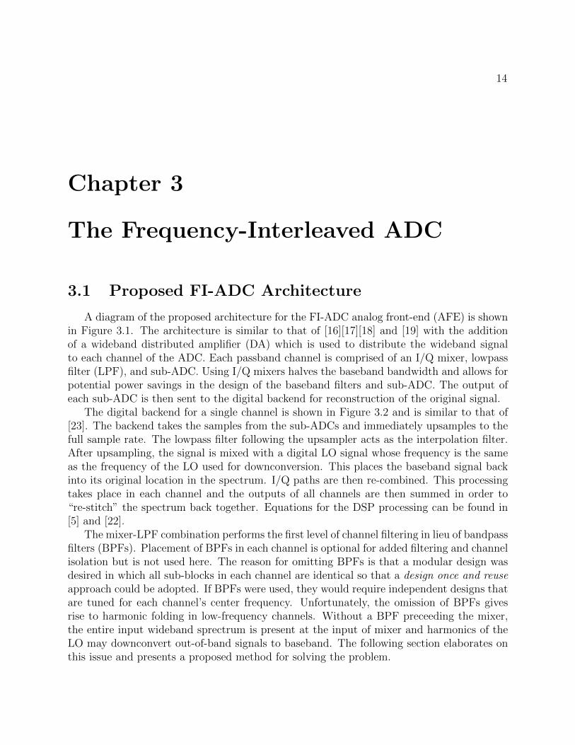
A diagram of the proposed architecture for the FI-ADC analog front-end (AFE) is shownin Figure 3.1. The architecture is similar to that of [16][17][18] and [19] with the additionof a wideband distributed amplifier (DA) which is used to distribute the wideband signalto each channel of the ADC. Each passband channel is comprised of an I/Q mixer, lowpassfilter (LPF), and sub-ADC. Using I/Q mixers halves the baseband bandwidth and allows forpotential power savings in the design of the baseband filters and sub-ADC. The output ofeach sub-ADC is then sent to the digital backend for reconstruction of the original signal.
The digital backend for a single channel is shown in Figure 3.2 and is similar to that of[23]. The backend takes the samples from the sub-ADCs and immediately upsamples to thefull sample rate. The lowpass filter following the upsampler acts as the interpolation filter.After upsampling, the signal is mixed with a digital LO signal whose frequency is the sameas the frequency of the LO used for downconversion. This places the baseband signal backinto its original location in the spectrum. I/Q paths are then re-combined. This processingtakes place in each channel and the outputs of all channels are then summed in order to“re-stitch” the spectrum back together. Equations for the DSP processing can be found in[5] and [22].
The mixer-LPF combination performs the first level of channel filtering in lieu of bandpassfilters (BPFs). Placement of BPFs in each channel is optional for added filtering and channelisolation but is not used here. The reason for omitting BPFs is that a modular design wasdesired in which all sub-blocks in each channel are identical so that a design once and reuseapproach could be adopted. If BPFs were used, they would require independent designs thatare tuned for each channel’s center frequency. Unfortunately, the omission of BPFs givesrise to harmonic folding in low-frequency channels. Without a BPF preceeding the mixer,the entire input wideband sprectrum is present at the input of mixer and harmonics of theLO may downconvert out-of-band signals to baseband. The following section elaborates onthis issue and presents a proposed method for solving the problem.

CHAPTER 3. THE FREQUENCY-INTERLEAVED ADC 15
Figure 3.1: Proposed FI-ADC Architecture.
Figure 3.2: Simplified processing for digital reconstruction.

CHAPTER 3. THE FREQUENCY-INTERLEAVED ADC 16
Key Challenges
Wideband Signal Distribution
Using a distibuted amplifier for distributing the signal to each channel is advantageoussince the capacitive loading of each channel is absorbed into the drain transmission line ofthe DA, resulting in a wider bandwidth distribution network. In contrary, if a single bufferwere used to drive all channels in parallel, the buffer would be extremely power hungrysince it has to drive a very large capacitance. Furthermore, the achievable bandwidth wouldultimately be limited by the fT of the process, whereas the bandwidth of the DA is limited bythe capacitive loading of each channel and the minimum inductance that can be accuratelyfabricated in the process (ignoring contraints on Zo). The latter is usually much larger thanthe former1. Another advantage of using a DA is that it breaks the gain-bandwidth tradeoffthat is faced by traditional amplifiers. This gives more freedom in the design, allowingfor optimized system noise figure, by increasing DA gain for example, without sacrificingbandwidth.
An alternative to the above distribution approaches would be a passive tree distibutionnetwork comprised of Wilkinson dividers (Figure 3.3). This approach has two attractivequalities: (1) wideband and (2) zero power consumption. The major drawback, however,is that the inherent insertion loss (IL) from the input to each channel increases with thenumber of channels, N. This is the case even if the Wilkinson divider is comprised of losslesspassives. The IL is further reduced once real, lossy passives are considered. Higher IL has adirect hit on the sensitivity of the ADC and results in a reduced dynamic range (resolution)for the ADC. As will be seen, the number of channels is a key design parameter in theoptimization of the ADC. Thus, it is desirable to de-couple the sensitivity of the ADC fromthe number of channels in order to allow more freedom in choosing the number of channels.For this reason, the passive power distribution approach is not used.
Figure 3.3: Wilkinson divider chain for broadband distribution.
1The extracted fT of modern 65nm CMOS processes is ∼ 200GHz, while the theoretical cutoff frequency,fc = 1
π√LC
, of an integrated transmission line would be ∼ 285GHz assuming L=50pH and C=25fF.

CHAPTER 3. THE FREQUENCY-INTERLEAVED ADC 17
Harmonic Folding
As previously mentioned, the proposed FI-ADC architecture is susceptible to harmonicfolding. Harmonic folding occurs in the proposed FI-ADC architecture for two reasons:(1) we are targeting larger than three channels and (2) there are no BPFs present beforedownconversion. These two design choices are critical for increasing the energy-efficiency ofthe architecture as well as simplifying the design. Due to the absence of bandpass filters,the full wideband signal is present at the RF input of the mixers. In an ideal mixer, the RFsignal is mulitplied by a perfect sinusoid whose frequency domain representation is a deltafunction at +wLO and −wLO. The output spectrum is then a sum of two frequency shiftedversions of the RF input – a shift right by wLO due to the delta function at −wLO and anidentical shift left due to the delta function at +wLO. After mixing, all energy around wLOis now located in the baseband (Figure 3.4). Note that by using a complex mixer, we caneffectively multiply the signal by a complex sinusoid (ejwt or e−jwt) and can extract eitherthe upper sideband or lower sideband information.
Figure 3.4: Harmonic folding corrupts the baseband signal.
CHAPTER 3. THE FREQUENCY-INTERLEAVED ADC 18
In the case of real mixing, where a simple Gilbert switching quad is used, we are mul-tiplying the RF signal with a square wave with a period of TLO. The spectrum of the LOsignal will thus have the fundamental tone along with its odd harmonics (3wLO, 5wLO, 7wLO,etc.)2. As a result, energy around these harmonics will also be downconverted to the base-band and corrupt our desired signal. In the context of the FI-ADC architecture, this is ahighly undesirable effect since our input signal is wideband and harmonics of the LO willlikely fall within the bandwidth of the signal and downconvert out-of-band energy.
The lower frequency channels of the FI-ADC are most susceptible to harmonic foldingsince a larger number of their harmonics are likely to fall within the bandwidth of the inputsignal. For a fixed input signal bandwidth, increasing the number of channels leads to alarger number of channels that are susceptible to harmonic folding. Roughly speaking, theith channel will have an LO frequency of
ωLO,i =i · ωmaxN
(3.1)
where ωmax is the maximum input frequency of interest and N is the number of channelsused in the FI-ADC. Considering the third harmonic of the LO, folding occurs if
3ωLO,i < ωmax (3.2)
or equivalently
i
N<
1
3(3.3)
Since 1 ≤ i ≤ N , it can be seen that harmonic folding is a non-issue for FI-ADCarchitectures with three or less channels (N ≤ 3). For N > 3, there are values of i forwhich the condition in Equation 3.3 is met. When N is increased, this condition is metfor a larger number of values for i (i.e. more channels experience harmonic folding of thethird harmonic). Similar conditions can be derived for the other harmonics of the LO. Thekey insight here is that increasing the number of channels exacerbates the harmonic foldingproblem. Since harmonic rejection techniques add complexity to the mixer design, there isa practical limit to how large N should be made.
Now, for an energy-efficient design, large N is desirable. Therefore, we will have tomitigate the impact of harmonic folding on our system performance. This can be done byutilizing harmonic rejection mixers (HRMs). Harmonic rejection techniques have been wellresearched in the context of wideband tranceivers for cellular and TV applications [25][26][27].The majority of these techniques are based on the topology proposed by Weldon [28]. Thecore idea is to emulate a multiplcation by a sampled-and-held sinusoid (SHS). The SHSwaveform can be produced by performing a weighted summation of phase shifted LO clock
2By using a differential topology in the mixer, the even-order components of the square wave are removedand only the odd-order components remain.

CHAPTER 3. THE FREQUENCY-INTERLEAVED ADC 19
signals. By emulating a sinusoid, the harmonic content of the LO reduces and, in the limit,the spectrum of the LO coverges to a single delta function.
As discussed in [28], the level of harmonic rejection depends on the accuracy of the LOphase shift and magnitude weightings. For cellular and TV applications, the LO fundamentalis typically below 1GHz. This allows for the usage of advanced digital techniques to generateaccurate multi-phase LO signals without consuming considerable amounts of power. This isnot the case for the wideband FI-ADC where the LO signals can easily be 3GHz or larger.For example, in our system the LO signals requiring harmonic rejection are 3 and 6GHz.At these frequencies, it is very difficult and power consuming to use digital techniques togenerate the multiple phases of the LO required for Weldon’s HRM architecture. Thus, weneed to design a HRM architecture that is capable of operating at higher LO frequencieswhile providing adequate harmonic rejection.
An architecture to acheive harmonic rejection at high LO frequencies is shown in Fig-ure 3.5. The high-frequency HRM (HF-HRM) architecture is comprised of a main mixer andan auxiliary mixer whose outputs are current-summed out-of-phase. The auxiliary mixer isdriven by the harmonic of the LO that we wish to cancel (in this example we are cancellingthe 3rd harmonic).
Figure 3.5: Block diagram of high frequency HRM.
From Figure 3.5 we see that the output spectrum of the main mixer consists of a cor-rupted baseband signal while the auxiliary mixer only produces the corrupting signal (energyaround 3ωLO in the baseband). By summing the two paths out-of-phase we can generate aclean baseband signal that is absent of harmonic folding. This architecture can be extendedto higher harmonic cancellation by adding additional auxiliary mixers that are driven by theharmonics to be cancelled. The appeal of this HRM design is that it fits naturally withinthe FI-ADC architecture since there is no overhead in the generation of the harmonic LOfrequencies – they are already generated since they will be the fundamentals for higher fre-quency channels and are readily available from the LO generation block. In conventional
CHAPTER 3. THE FREQUENCY-INTERLEAVED ADC 20
cellular/TV receivers, the harmonics of the LO are not readily available, making this ap-proach unattractive for such systems.
As with any noise/interference technique that relies on the summation of two paths, gainand phase mismatch of the two paths limit the attainable level of cancellation. Furtherdiscussion of the HF-HRM and its design are provided in the next chapter.
LO Generation/Distribution
A major overhead in the FI-ADC design is the generation and distribution of the multipleLO frequencies needed for downconversion. For frequency generation, QVCO-based PLLscan be utilized for the highest required LO frequency. The frequency divider chain embeddedinside the PLL can then be tapped to access the LO frequencies that are integer-related tothe fundamental frequency. For example, the highest LO frequency required in this design is24GHz and the 12GHz, 6GHz and 3GHz LOs required by other channels would be availablefrom the dividers in the PLL. The challenge here is generating the frequencies that have anon-integer relation to the PLL fundamental frequency (e.g. generating 18GHz from 24GHz).In addition, all LOs must be phase locked so that the phase delay between channels doesn’tdrift over time and won’t cause any errors during the reconstruction of the signal.
In this design, fundamental frequency generation wasn’t performed since there have beenworks demonstrating the feasibility of designing low-power (< 50mW), very high-frequency(> 20GHz) PLLs in modern CMOS processes [14][15]. However, generation of all other LOfrequencies (assuming two phase-locked fundamental frequencies are available) is performedon chip and techniques for generating the non-integer related frequencies are presented inChapter 4.
Once the LO frequencies have been generated, the next challenge is in distributing theLO to the mixer inputs. As will be seen later in this chapter, LO phase noise plays a criticalrole in the performance of the FI-ADC and must be properly managed in order to achieveperformance gains over the TI-ADC. As a result, any buffers used in distributing the LOmust not add significant noise/jitter to the LO. This can result in high power consumptionin the LO buffers. Thus, the number of LO buffers used should be minimized. Furthermore,care must be taken in the distribution of the highest LO frequencies in order to minimizesignal loss. As such, transmission lines must be utilized and the floorplanning must bearchitected to minimize the trace lengths of these high-frequency signals.
Lastly, with numerous LOs being generated and distributed across the chip, crosstalkis another major concern. Any spurious tones that arise as a result of crosstalk betweenLO distribution lines will result in downconversion of spectrum from other channels, anundesirable effect. To meet system specifications, the crosstalk between LOs needs to bebelow ∼ 45dB so that the undesired downcoverted spectrum falls below the noise floor. Tomeet these specs, proper layout techniques and floorplanning must be employed. Techniquesfor minimizing the LO crosstalk are presented in Chapter 4.
CHAPTER 3. THE FREQUENCY-INTERLEAVED ADC 21
Digital Reconstruction
Proper reconstruction of the signal in the digital domain is another challenge in the FI-ADC. Although it is claimed that the FI architecture is less senstivite to channel mismatchesthan the TI architecture [5], equalization across channels is still necessary for applicationsrequiring real-time reconstruction of a wideband signal. For a single-firequency excitation3,the FI architecture will show better performance than the TI architecture because the outputstream is given from a single channel as opposed to being a composite of output streamsfrom various channels. In this case, the FI architecture does not require equalization acrosschannels and only needs to equalize the I/Q paths within each channel for proper imagerejection. On the other hand, for a wideband excitation (e.g. narrow-width pulse), multiplechannels will contribute to the FI architecture’s output and will therefore need to haveidentical performance so as to not introduce distortion when recreating the time-domainsignal. As far as the AFE is concerned, the gain and group delay of all channels should beequal to allow the digital backend to perform proper reconstruction.
In addition, the AFE still needs to retain suffiicient gain and phase matching betweenthe I and Q paths within in each channel in order to achieve adequate image rejection.Gain/phase mismatch results in finite image rejection. For a 6b system, the desired imagerejection is > 40dB. In order to obtain this level of rejection, the gain and phase of I/Qpaths must match within 0.1dB and 1, respectively.
Digital reconstruction and equalization techniques are not the focus of this work andany equalization required in the backend is performed offline in a manual fashion. Fur-thermore, [22] has proposed digital compensation techniques for channel mismatch in thedownconverting FI architectures. As will be seen in the next chapter, many design decisionsfor the implemented FI-ADC were made with the intent to minimize the amount of digitalcompensation required.
3This is the standard excitation used for testing ADC performance. However, it should be noted that itis not sufficient to fully compare the FI and TI architectures.

CHAPTER 3. THE FREQUENCY-INTERLEAVED ADC 22
3.2 FI-ADC vs. TI-ADC
One of the key merits of FI-ADCs is the potentital to break the jitter barrier faced byconventional sampling architectures. By limiting the bandwidth of the signal presented tothe sample-and-hold circuitry, the jitter requirement on the sampling clock for achievinga specific ENOB is relaxed. In order to reduce the required sub-ADC sampling rate forpassband channels, mixers are used to downconvert the passband channels to basebandand allow for a lower sampling rate to be used. Consequently, this “mix-then-sample”architecture has introduced a new process that isn’t present in conventional ADC samplingarchitectures - mixing - and it is worth exploring how the two approaches compare.
The following sections present both a qualitative and quantitative comparison of the FI-ADC to the TI-ADC. First, conventional ADC sampling (direct-sampling) is compared tothe mix-then-sample architecture in terms of noise performance and ENOB as a function ofinput frequency. Next, a detailed discussion on the impact of LO phase noise is presentedfollowed by results from a system-level simulation. The simulation is used to accuratelycompare the FI-ADC to conventional direct-sampling architectures.
Direct Sampling vs. Mix-then-sample
It is of interest to compare the FI-ADC’s mix-then-sample (MTS) front-end architectureto a direct-sampling (DS) architecture which feeds the wideband input signal directly into aNyquist rate sampler (Figure 3.6).
Figure 3.6: Sampling architectures: (top) Direct-sampling and (bot) Mix-then-sample.
In the DS approach (Figure 3.6(a)), the wideband signal is fed directly into a samplerthat samples the signal at the Nyquist rate of 2 · fin,max and then passes the sampled signalto a quantizer. In the MTS approach, the input signal is downcoverted by an LO signal,low-pass filtered, sampled at the baseband Nyquist rate of 2 · fIF,max ≈ 2 · fin,max
2Nand then

CHAPTER 3. THE FREQUENCY-INTERLEAVED ADC 23
quantized. The lowpass filter has a cutoff frequency dictated by the sub-channel bandwidthand limits the maximum frequency presented to the sampler to
fin,max
2N, where N is the
number of channels in the FI-ADC4. We are now interested in comparing the two samplingarchitectures performance in regards to three metrics: (1) input noise, (2) ENOB v. inputfrequency, and (3) LO phase noise at the mixer input.
The impact of LO phase noise is of considerable interest. This is because the LO phasenoise is transferred to the input signal during the mixing process and although we areless senstivite to jitter at the sampling instant, the jitter problem may have simply beentransformed into a phase noise problem at the mixing instant. Almost all publicationsrelated to the FI architecture simply cite the decreased jitter sensitivitiy with no mentionof the impact of phase noise. [19] does address this issue, but simply shows, via simulationresults, that the sampling jitter was more a performance limiter than the “mixing jitter” andtherefore they do not provide any detailed discussion on how the “mixing jitter” impacts thesystem. Similarly, [21] presents encouraging simulation results that incorporate LO phasenoise but offers no supporting discussion. Here, we provide a quantitative discussion of theimpact of LO phase noise.
Input Noise
One of the drawbacks of the MTS architecture is that it has a worse response to inputnoise than the direct-sampling architecture. The reason for the degraded response is noisefolding that occurs during the mixing process. This can be better understood from Figure 3.7which shows the spectrum of the input noise at the input of the mixer in the first passbandchannel (chan1) of a five channel architecture. Here, the input noise bandwidth is assumedto be limited to the maximum signal bandwidth, fin,max. This is a legitimate assumptionsince all sampling systems have an anti-aliasing filter5 placed before the sampler in orderto prevent out-of-band signals from aliasing down to baseband and corrupting the desiredsignal. As a result, the input noise spectrum will be containted within this bandwidth andzero beyond that.
Due to lack of bandpass filters before the mixer, the entire input noise spectrum is presentat the RF port of the mixer. The fundamental LO frequency, fLO,1 ,will be centered in chan1and downconvert the noise spectrum in its passband down to baseband. In addition, thethird harmonic will also fall within chan3’s passband and any noise in chan3’s passband willalso be downconverted to baseband. In the ideal case, we only want to process the noiselocated in the passband dedicated to that channel, but due to real mixing, the noise aroundthe harmonics of the LO will also be folded down to baseband and degrade the SNR. Noisefolding is identical to the harmonic folding problem since they both stem from the samenon-ideality - harmonics of the LO downconverting out-of-band spectrum during the mixing
4The additional factor of 2 is due to the fact that we are using I/Q mixers which further cuts the basebandbandwidth in half
5An ideal anti-aliasing filter is a brickwall lowpass filter with a bandwidth equal to the maximum fre-quency of interest.

CHAPTER 3. THE FREQUENCY-INTERLEAVED ADC 24
Figure 3.7: Input noise spectrum for mix-then-sample.
process. This means that the input-noise folding problem can also be mitigated by usingharmonic-rejection mixers.
The DS architecture does not suffer from this issue of input noise folding. This can beeasily seen by observing typical noise input spectrum for the DS case (Figure 3.8).
Figure 3.8: Input noise spectrum for direct-sampling.
An anti-aliasing filter will limit the noise bandwidth to fin,max and the sampling clock’sLO frequency is located at the Nyquist sample frequency of 2 · fin,max. As can be seen inFigure 3.8, the fundamental tone of the sampling clock falls out of band of the input noiseand thus all the subsequent harmonics that comprise the spectrum of the sampling processwill also fall out of band and there will be no noise folding in the direct sampling system.
ENOB vs. fin
As illustrated in [18], the FI-ADC can maintain close to peak ENOB across the entireinput frequency range as opposed to the TI-ADC which exhibits a degradation in ENOB asthe input frequency approaches the Nyquist frequency. This superior ENOB performance isattributed to the bounds placed on the signal frequency at the input of the sampler.
CHAPTER 3. THE FREQUENCY-INTERLEAVED ADC 25
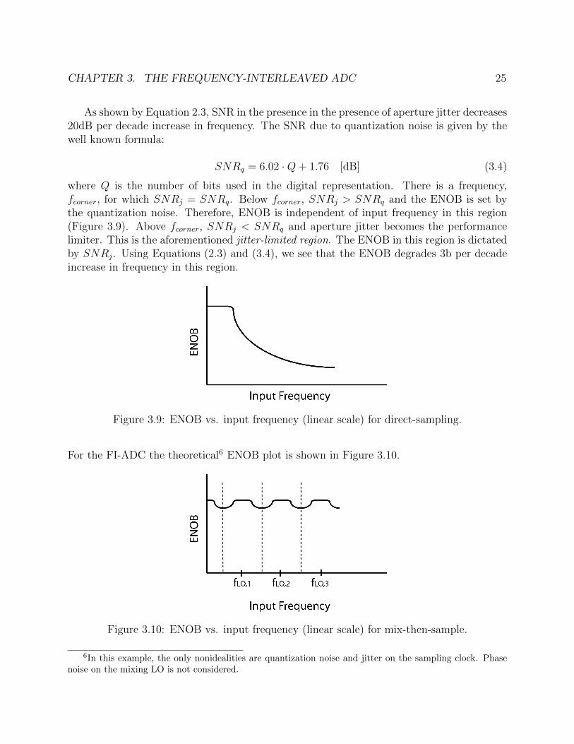
As shown by Equation 2.3, SNR in the presence in the presence of aperture jitter decreases20dB per decade increase in frequency. The SNR due to quantization noise is given by thewell known formula:
SNRq = 6.02 ·Q+ 1.76 [dB] (3.4)
where Q is the number of bits used in the digital representation. There is a frequency,fcorner, for which SNRj = SNRq. Below fcorner, SNRj > SNRq and the ENOB is set bythe quantization noise. Therefore, ENOB is independent of input frequency in this region(Figure 3.9). Above fcorner, SNRj < SNRq and aperture jitter becomes the performancelimiter. This is the aforementioned jitter-limited region. The ENOB in this region is dictatedby SNRj. Using Equations (2.3) and (3.4), we see that the ENOB degrades 3b per decadeincrease in frequency in this region.
Figure 3.9: ENOB vs. input frequency (linear scale) for direct-sampling.
For the FI-ADC the theoretical6 ENOB plot is shown in Figure 3.10.
Figure 3.10: ENOB vs. input frequency (linear scale) for mix-then-sample.
6In this example, the only nonidealities are quantization noise and jitter on the sampling clock. Phasenoise on the mixing LO is not considered.

CHAPTER 3. THE FREQUENCY-INTERLEAVED ADC 26
To best understand how this plot is generated, consider an input frequency equal tothe LO frequency of the first channel, fLO,1. After mixing, the signal is translated to aDC baseband frequency (0 Hz). Because this is a very low frequency, SNR will be set bySNRq. As the frequency is increased (or decreased) slightly, the ENOB will remain flatsince the baseband frequency, |fLO,1− fin|, will still be a relatively low frequency. Increasing(or decreasing) the input frequency further, the baseband frequency becomes larger and wewill enter the jitter-limited region and the ENOB will begin to degrade just like Figure 3.97.However, unlike Figure 3.9 where the ENOB degrades indefinitely, the ENOB degradationwill hit a minimum at the channel’s frequency edge. Above that frequency, the input signalis now processed by the adjacent channel and will begin approaching that channel’s LOfrequency. For example, increasing the input frequency will push the input signal intochannel 2 and the new baseband frequency is |fLO,2 − fin| which decreases in magnitudeuntil fin = fLO,2. A decrease in baseband frequency leads to an increase in ENOB and aneventual re-entry into the quantization-limited region. After this point, the behavior repeatsitself.
So to first-order, it appears that the FI-ADC can provide a relatively constant ENOBover the entire Nyquist frequency band. When LO phase noise is considered, this is notthe case, and slight degradation in ENOB at higher frequencies may be observed. Interest-ingly, enough, the FI-ADC can still outperform the TI-ADC even when this high-frequencydegradation is taken into account. There are many factors that determine the true relativeENOB performance in the presence of LO phase noise and sampling jitter. The followingdiscussions elaborate on this topic.
Impact of LO Phase Noise
The last, and most important, point of comparison is the impact of LO phase noise. Thekey argument for the FI architecture is the potential for breaking the jitter barrier whichplagues current high-speed ADCs. In order to do so, we have downconverted and lowpassfiltered the signal before sampling. This limits the bandwidth of the signal going into thesampler and hence, relaxes the sensitivity to the jitter on the sampling clock. The questionhere is: what impact does the LO phase noise have on the noise performance down thechain. Afterall, phase noise and jitter are closely related. Also, it is likely that the LOused for downconversion and the sampling clock are derived from a common source and willhave similar phase noise/jitter performance. So it isn’t clear if there is a net gain since wepotentially have a phase noise constraint on the mixing LO and this may be equivalent tothe jitter constraint on the sampling clock in the DS achitecture.
Before we assess how LO phase noise impacts the noise performance of the MTS archtiec-ture, we first derive how jitter at the sampling instant limits the SNR performance of the DSarchitecture. This analysis will be valuable when we want to assess the SNR performance of
7Depending on the amount of sampling jitter, σj , and the channel bandwidths, there is a possiblity thatthe jitter-limited region is never observed

CHAPTER 3. THE FREQUENCY-INTERLEAVED ADC 27
the MTS archtiecture. First, we observe that any timing error (i.e. jitter) on the samplingclock will result in an error in the sampled voltage of the input signal (Figure 3.11).
Figure 3.11: Timing error on sampling clock translates to a voltage error proportional to theslope of the signal.
The voltage error is proportional to the slope of the signal and is given by [29]:
verr(t) =ds(t)
dt· σjitter (3.5)
where s(t) is the input signal being sampled and σjitter is the rms-jitter on the the samplingclock. The signal output of the sampler will consist of the desired signal, s(t), and the errorsignal, verr(t). Assuming a single sinusoid at the input:
vout,DS(t) = s(t) + verr(t) (3.6a)
= A cos(2πfint) + A2πfinσjitter sin(2πfint) (3.6b)
To obtain the SNR, we take the ratio of the power in the desired signal to power ofthe error signal. Note that in the time domain, the error signal is a sinusoid of amplitdueA2πfinσjitter and is phase shifted by 90 w.r.t. the input signal. Intuitively, this makes sensesince the error signal should be largest at the zero crossings of the input sinusoid. Takingthe ratio of signal powers from Equation 3.6b, we get:
S
N=
(A√2
)2
(A2πfinσjitter√
2
)2 =1
(2πfinσjitter)2 (3.7)
Or equivalently in dB:

CHAPTER 3. THE FREQUENCY-INTERLEAVED ADC 28
SNR = −20 log(2πfinσjitter) [dB] (3.8)
This is the well-known classical result that says that for a given jitter on the samplingclock, σjitter, the SNR of a jitter-limited system degrades 20dB/decade w.r.t. input frequency.In order to avoid operating in the jitter-limited regime, the SNR due to jitter (Equation 3.8)needs to be greater than the SNR due to quantization noise (Equation 3.4). As an example,to obtain 6b of resolution for a 25GHz signal the rms-jitter would have to be less than123fs-rms.
The above analysis provides the mathematical evaluation of the SNR at the samplinginstant. In order to evaluate the SNR of the entire MTS chain, we can take a two-stepapproach. First, we determine the expression for the analog signal at the ouput of thelow-pass filter, vLPF (t). Next, we substitute s(t) with vLPF (t) in Equation 3.6b and followthe analysis used above for evaluating SNR since vLPF (t) is now the input of our basebandsampler.
At the output of the mixer, we have a multiplication between our input sinusoid and theLO with phase noise. For simplicity, we choose the amplitudes of the input signal and LOin such a way that the baseband amplitude becomes unity. Thus, we have at the output ofthe mixer:
vmix(t) = vin(t) · vLO(t) (3.9a)
= cos(2πfint) · 2 cos(2πfLOt+ φ(t)) (3.9b)
= cos(2π(fin − fLO)t− φ(t)) + cos(2π(fin + fLO)t+ φ(t)) (3.9c)
The lowpass filter will filter the components at the sum frequency, fin + fLO, and thusat the output of the LPF we have:
vLPF (t) = cos (2π(fin − fLO)t− φ(t)) (3.10a)
= cos (φ(t)) cos(2πfIF t) + sin (φ(t)) sin(2πfIF t) (3.10b)
= cos(2πfIF t) + φ(t) sin(2πfIF t) (3.10c)
where fIF = |fin − fLO| is the baseband intermediate frequency (IF) and we have used thesmall angle approximations cos(φ(t)) ≈ 1 and sin(φ(t)) ≈ φ(t).
Observing Equation 3.10c, we see that after lowpass filtering we have the desired basebandsignal along with the LO phase noise modulated up to the IF frequency. In essence, the phasenoise profile of the LO signal has been transferred to the baseband signal (Figure 3.12).

CHAPTER 3. THE FREQUENCY-INTERLEAVED ADC 29
Figure 3.12: Mixing of input signal and LO with phase noise.
Equation 3.10c is now the expression for the input signal to the sampler. The samplerin the MTS system samples at the baseband Nyquist rate of 2 · fIF,max ≈ 2 · fin,max
2N. Using
Equation 3.5 and Equation 3.6b, and substituting s(t) in these equations with vLPF (t) fromEquation 3.10a, we can determine the signal at the output of the sampler:
vout,MTS(t) = vLPF (t) +δ(vLPF (t))
δt· σjitter (3.11a)
= cos(2πfIF t) + φ(t) sin(2πfIF t) + σjitter
[2πfIF −
δφ(t)
δt
]sin(2πfIF t− φ(t))
(3.11b)
The first two terms on the right hand side of Equation 3.11b are directly from the vLPFexpression and represent the baseband signal (first term) along with the additive noise in-troduced during the mixing process (second term). The last term is the voltage error causedby sampling a non-zero slope signal using a clock with jitter.
One thing to note at this point is that the presence of the second term is new as comparedto Equation 3.6b. There, we only had two terms – the desired signal and the error due tojitter. Here, even if we sample the signal with a perfect clock (σjitter = 0), we will still havethe downconverted phase noise that will degrade the SNR at the output of the sampler.For the DS case (Equation 3.6b), σjitter = 0 would result in an infinite SNR (i.e. no SNRdegradation due to sampling) and the system performance would then be dictated by thequantization noise. Thus, it is apparent that the presence of this second term plays acrucial role in determining the net benefit of the MTS architecture over the conventionalDS architecture and we will return to this discussion. But first, we can further simplifyEquation 3.11b by analyzing the various parts of the third term.
The third term represents the voltage error due to jitter on the sampling clock and, asdiscussed earlier, is proportional to the radian frequency of the signal being sampled. The

CHAPTER 3. THE FREQUENCY-INTERLEAVED ADC 30
two expressions in brackets are measures of the radian frequency; the first term is the abso-lute frequency of 2πfIF while the second term represents the uncertainty in instantaneousfrequency due to the phase noise. As such, the second term can be thought of as the effectivewidening of the spectrum that occurs when phase noise is present on a tone. For generaloscillators, this widening is generally contained to a very small fraction of the absolute fre-quency because it would otherwise render it useless in any communication system. This isbecause the spectrum of the oscillator should not spill over into adjacent channels since itwould lead to downconversion of out-of-band signals, thereby corrupting the baseband signal.Therefore, this second term is typically much less than the first term and can be ignored.Equation 3.11b then becomes:
vout,MTS(t) = cos(2πfIF t) + φ(t) sin(2πfIF t) + σjitter2πfIF sin(2πfIF t− φ(t)) (3.12)
Using the identity sin(u − v) = sin(u) cos(v) − cos(u) sin(v) the third expression in Equa-tion 3.12 can be expanded:
= σjitter2πfIF [sin(2πfIF t) cos(φ(t))− cos(2πfIF t) sin(φ(t))] (3.13a)
= σjitter2πfIF [sin(2πfIF t)− φ(t) cos(2πfIF t)] (3.13b)
The second term in (3.13b) will produce a term similar to the second term in (3.12). Bothterms represent a modulated version of φ(t) up to the IF frequency. However, the additionalfactor of 2πfIFσjitter in (3.13b) will make its term less significant and we can therefore ignoreit for the purpose of simplifying the analysis8. Plugging the first part of (3.13b) into (3.12),we arrive at our final expression for the signal at the output of the sampler:
vout,MTS(t) = cos(2πfIF t) + φ(t) sin(2πfIF t) + σjitter2πfIF sin(2πfIF t) (3.14)
In order to calculate the SNR of this signal we need to evaluate the power of the desiredsignal (first term) and the noise/error signals (last two terms). The powers of the firstand third terms are straightforward to calculate (same calculation as in (3.7)). As for thesecond term, φ(t) is a stochastic process that can be fully described by it’s frequency domainrepresentation, L (f), which is the SSB phase noise spectrum commonly used to characterizeoscillator phase noise. Using Parseval’s theorem, we can calculate the power of this signalby integrating in the frequency domain [30][31]:
φ2n = 2 ·
∫ ∞0
10L (f)/10 df [radians2] (3.15)
The rms value of the phase noise is then given by:
φn =
√2 ·∫ ∞
0
10L (f)/10 df [radians] (3.16)
8As an example, for fIF = 1.5GHz and σjitter = 1ps rms, 2πfIFσjitter ≈ 10−2 which is enough to makethis term insiginicant when compared to the second term in (3.12)

CHAPTER 3. THE FREQUENCY-INTERLEAVED ADC 31
In both equations, the SSB phase noise, L (f), is first converted to linear units beforebeing integrated. The factor of two in both equations is needed to capture integration acrossboth sidebands since L (f) is a SSB spectrum. Now that we have the power of each term in(3.14), we can solve for the SNR of the MTS architecture:
S
N≈ 1
(2πfIFσjitter)2 +(
2 · φ2n
) (3.17)
Comparing (3.17) to (3.7), there are apparent similarities and differences. Ignoring, the φ2n
term, the two equations are almost identical. This, of course, comes as no surprise since theyare modeling the same nonideality - voltage error due to non-zero slope. The only differencehere is that the fin in (3.7) has been replaced by fIF . Since fin can be as high the fullNyqusit frequency, fmax, while fIF is bounded to roughly 1
Nof this maximum frequency9,
we see that there is an immediate gain in SNR of N2. This is the desired result we weretargeting. We have bounded the frequency of the signal that is subject to the jitter on thesampling clock. As a result, the resultant rms voltage error due to jitter at the samplinginstant has been significantly reduced and we can now obtain larger SNR after sampling inthe presence of a given σjitter.
Unfortunately, this is not the end of the story due to the presence of the φ2n which takes
away from our immediate N2 SNR gain. Due to the presence of the φ2n term, we take a
penalty in SNR for low input frequencies and the DS architecture actually outperforms theMTS architecture. This is because for values of fin ≤ fIF , the 2πfIF (in)σjitter terms are equal
in both SNR equations and thus the φ2n term knocks the SNR of the MTS architecture below
that of the DS architecture.As fin is increased to higher frequencies, (3.7) continues to decrease without bound, while
the worst-case value for (3.17) is:
S
N≈ 1
(2πfIF,maxσjitter)2 +(
2 · φ2n
) (3.18)
where fIF,max is the maximum IF frequency (≈ fmax
2N). Thus, there is a crossover frequency
where the MTS SNR becomes larger than the DS SNR and the SNR gain continues toincrease with increasing fin. Since φ2
n acts as a “one-time hit”, the higher the value of thisintegrated phase noise, the higher the crossover frequency past which it makes sense to usethe MTS architecture over the DS (Figure 3.13). This means that the phase noise of the LOcannot be ignored in the design of the MTS architecture and care should be taken to ensurethat the crossover frequency is low enough such that the MTS architecutre make sense forthe given application. For example, if the application requires digitization of signals up to10GHz yet the crossover frequency is 9GHz, then it may not make much sense to implementthe MTS architecture since it’s providing very marginal gains for frequences between 9 and
9Assuming that the wideband spectrum is dissected to N sub-bands of equal bandwidths.
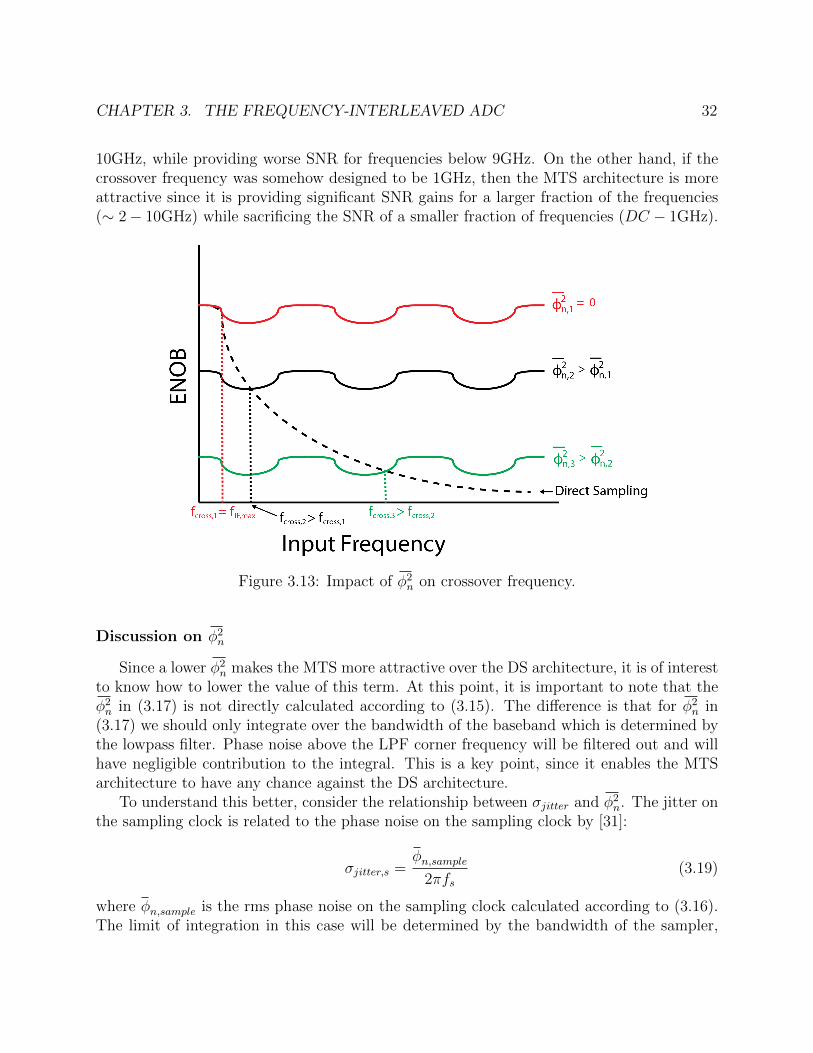
CHAPTER 3. THE FREQUENCY-INTERLEAVED ADC 32
10GHz, while providing worse SNR for frequencies below 9GHz. On the other hand, if thecrossover frequency was somehow designed to be 1GHz, then the MTS architecture is moreattractive since it is providing significant SNR gains for a larger fraction of the frequencies(∼ 2− 10GHz) while sacrificing the SNR of a smaller fraction of frequencies (DC − 1GHz).
Figure 3.13: Impact of φ2n on crossover frequency.
Discussion on φ2n
Since a lower φ2n makes the MTS more attractive over the DS architecture, it is of interest
to know how to lower the value of this term. At this point, it is important to note that theφ2n in (3.17) is not directly calculated according to (3.15). The difference is that for φ2
n in(3.17) we should only integrate over the bandwidth of the baseband which is determined bythe lowpass filter. Phase noise above the LPF corner frequency will be filtered out and willhave negligible contribution to the integral. This is a key point, since it enables the MTSarchitecture to have any chance against the DS architecture.
To understand this better, consider the relationship between σjitter and φ2n. The jitter on
the sampling clock is related to the phase noise on the sampling clock by [31]:
σjitter,s =φn,sample
2πfs(3.19)
where φn,sample is the rms phase noise on the sampling clock calculated according to (3.16).The limit of integration in this case will be determined by the bandwidth of the sampler,
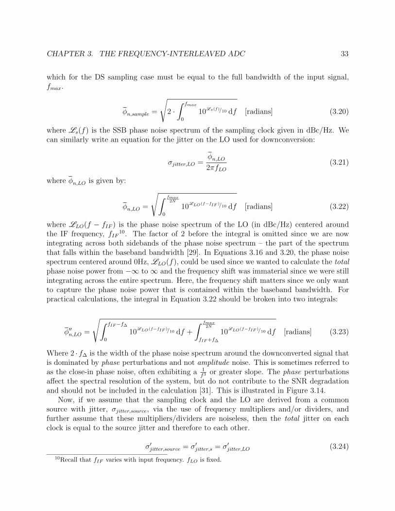
CHAPTER 3. THE FREQUENCY-INTERLEAVED ADC 33
which for the DS sampling case must be equal to the full bandwidth of the input signal,fmax.
φn,sample =
√2 ·∫ fmax
0
10Ls(f)/10 df [radians] (3.20)
where Ls(f) is the SSB phase noise spectrum of the sampling clock given in dBc/Hz. Wecan similarly write an equation for the jitter on the LO used for downconversion:
σjitter,LO =φn,LO2πfLO
(3.21)
where φn,LO is given by:
φn,LO =
√∫ fmax2N
0
10LLO(f−fIF )/10 df [radians] (3.22)
where LLO(f − fIF ) is the phase noise spectrum of the LO (in dBc/Hz) centered aroundthe IF frequency, fIF
10. The factor of 2 before the integral is omitted since we are nowintegrating across both sidebands of the phase noise spectrum – the part of the spectrumthat falls within the baseband bandwidth [29]. In Equations 3.16 and 3.20, the phase noisespectrum centered around 0Hz, LLO(f), could be used since we wanted to calculate the totalphase noise power from −∞ to∞ and the frequency shift was immaterial since we were stillintegrating across the entire spectrum. Here, the frequency shift matters since we only wantto capture the phase noise power that is contained within the baseband bandwidth. Forpractical calculations, the integral in Equation 3.22 should be broken into two integrals:
φ′′n,LO =
√∫ fIF−f∆
0
10LLO(f−fIF )/10 df +
∫ fmax2N
fIF +f∆
10LLO(f−fIF )/10 df [radians] (3.23)
Where 2 · f∆ is the width of the phase noise spectrum around the downconverted signal thatis dominated by phase perturbations and not amplitude noise. This is sometimes referred toas the close-in phase noise, often exhibiting a 1
f3 or greater slope. The phase perturbationsaffect the spectral resolution of the system, but do not contribute to the SNR degradationand should not be included in the calculation [31]. This is illustrated in Figure 3.14.
Now, if we assume that the sampling clock and the LO are derived from a commonsource with jitter, σjitter,source, via the use of frequency multipliers and/or dividers, andfurther assume that these multipliers/dividers are noiseless, then the total jitter on eachclock is equal to the source jitter and therefore to each other.
σ′jitter,source = σ′jitter,s = σ′jitter,LO (3.24)
10Recall that fIF varies with input frequency. fLO is fixed.

CHAPTER 3. THE FREQUENCY-INTERLEAVED ADC 34
Figure 3.14: LO phase noise power w/o close-in phase noise.
where primed notation is used to indicate the total integrated jitter from 0 to ∞:
σ′j =
√2 ·∫∞
010L (f)/10 df
2πf(3.25)
Using (3.24) and the primed versions of (3.19) and (3.21) we can write an expression relatingthe phase noise of the LO to the jitter on the sampling clock:
φ′n,LO = 2πfLO · σ′jitter,s (3.26)
Before we continue, let’s take a step back to remind ourselves that these primed variables,which denote integration from 0 to ∞, are representative of the MTS sytem without a LPFin the baseband. Without the LPF, the limit of integration is no longer set by the IFbandwidth and is instead integrated up to the highest frequency with non-neglible phasenoise. Generally, this limit would be fmax since that’s the highest bandwidth any nodein either architecture has to achieve, but we lose nothing by integrating to ∞. The keytakeway here is that without the LPF, all of the phase noise that was integrated in the DSarchitecture to determine jitter, is also integrated when determining the noise added duringthe mixing process. Immediately, it becomes apparent that, with baseband LPFs omitted,it is implausible that the MTS architecture can outperform the DS architecture since we aresubjecting ourselves to the phase noise twice – once at the mixing node and again at thesampler. This is seen by plugging (3.26) into (3.17) and simplifying:
S
N ,noLPF≈ 1
(2πσ′jitter)2 · (f 2
IF + 2f 2LO)
(3.27)
Comparing (3.27) to (3.7) and plugging in the best-chance scenario of fin = fLO+fin,max
2N11
it can be shown that (3.27) is always less than (3.7), except for a subset of frequencies in the
11For a given channel in the MTS architecture, the DS SNR is minimized at the edge frequency.
CHAPTER 3. THE FREQUENCY-INTERLEAVED ADC 35
first channel. Another takeaway from (3.27) is that the SNR degrades as we go to higherfrequency channels (larger fLO). We will later see that this general behavior holds with theLPF present12. Further analysis of this “LPF-omitted” scenario is not done here since it isnot representative of the true MTS architecture.
In the real MTS architecture, the LPF is a integral part of the operation and is whatallows the escape from the grim prospect of re-introducing all of the phase noise at the mixer.With the LPF, (3.24) no longer holds since the limits of integration are given according to(3.20) and (3.22) and we can now write:
σjitter,LO < σjitter,s (3.28)
The key variable in determining the magnitude of this inequality, is the number of chan-nels, N . With a larger number of channels, the limit of integration in (3.22) becomes smaller,resulting in a smaller φn,LO and hence a smaller “one-time” hit in SNR. As a result, we canreduce the crossover frequency and make the MTS architecture beneficial for a larger rangeof frequencies. Of course other problems arise with increasing N , and there is a practicallimit to how large N should be made.
Aside: Using direct-sampling as a basis for comparison
The direct-sampling architecture is a good basis for comparison as it captures the con-straints and fundamental performance trends that we are interested in assesing for allNyquist-rate ADC architectures – bandwidth requirements, ENOB vs. frequency, and noiseperformance. This is easy to see for single-channel architectures since their front-end willclosely resemble that of Figure 3.6(a). Furthermore, one can argue that single-channel sam-pling sets the upper-bound on the performance of multi-channel architectures (i.e. time-interleaved) with the same effective sample rate, if we neglect power consumption. First,the multi-channel architectures degrade the noise performance as compared to single-channelsince there are more components and thus, more noise sources needed to process the signal.The bandwidth requirements of multi-channel is the same as single-channel since the fullsignal bandwidth needs to be passed to all channels even though the sub-channel samplerate is lower. Thus, the same bandwidth requirement is placed on the front-end T/H am-plifier. Lastly, if we assume a perfect quantizer, then the ENOB performance is determinedby the jitter of the sampling clock and the maximum input frequency, both of which are thesame for multi-channel and single-channel architectures. Therefore, the DS architecture is aproper basis for comparison.
12Assuming certain conditions on the LO phase noise.

CHAPTER 3. THE FREQUENCY-INTERLEAVED ADC 36
System-Level Simulations
Simulation Setup
In order to assess the performance FI-ADC as compared to the TI-ADC and other DSarchitecures, a system level simulation was performed using Keysight’s SystemVue software.A block diagram of the models used for comparison is shown in Figure 3.15.
Figure 3.15: Block diagram of models used for system simulation.
For the DS architecture, a model similar to that of Figure 3.6 is used. The samplingfrequency is chosen to be 50GS/s for an input Nyquist frequency of 25GHz. An 8-bit ADCis used to sample and quantize the input signal. For the FI-ADC system, an 8-channelarchitecture is chosen with passband bandwidths of 3GHz. The IF frequency is cut downto 1.5GHz by using complex (I/Q) downconversion (not shown in Figure 3.15). The LOfrequencies are integer multiples of 3GHz up to 24GHz (i.e. 3,6,9...21,24). The basebandfilters are 6th order Butterworth filters with a corner frequency of 2GHz. The output of

CHAPTER 3. THE FREQUENCY-INTERLEAVED ADC 37
each LPF is oversampled (2.35x) and quantized by an 8-bit ADC13. The I/Q outputs of eachchannel is then sent to the digital backend to perform signal reconstruction and output asingle stream of data. An FFT is then performed on the output streams of each system andthe SNRs at each output are compared.
The clocks used for sampling and downconversion are all related in a manner similar towhat is depicted in Figure 3.15. The only difference being that all sources have uncorrelatedphase noise whereas Figure 3.15 suggests that the phase noises of the clocks are correlated.The LO chain begins with the master frequency of 50GHz used to drive the ADC in the DSarchitecture. The phase noise of this sampling clock is defined such that it integrates to adesired σjitter. Next, we want to assess if the FI-ADC architecture can perform better in thepresence of the same σjitter. Given this, we derive the phase noise of each subsequent LOfrequency such that it’s phase noise integrates to the same σjitter
14. The assumption hereis noiseless frequency division. The jitter on the sampling clocks for the FI-ADC are alsoequal to the same σjitter. Lastly, low Q bandpass filters (2nd order, Q=4) are placed on theLO paths before driving the mixers. These filters are representative of the resonant tanksthat would typically be used in the LO chain to drive the mixer LO ports with large swingsinusoids.
Simulation Results
Given this simulation setup, the input frequency to each system was swept and the outputSNR analyzed for a single-tone excitation. This sweep was performed with σjitter = 200fsand σjitter = 400fs. The results from this simulation are shown in Figure 3.16. In this plot,the jitter-limited behavior of the DS architecture (dotted lines) is immediately apparent.The SNR degrades at a rate of 20dB/decade for frequencies well past the corner frequency.
For the MTS architecture (solid lines), the SNR does degrade slightly as the input fre-quency is increased, but the degradation is not as severe as the DS case. At the Nyqusitrate, we see a 15dB improvement in SNR over the DS architecture which is equivalent to2.5b of added ENOB. Note that the SNR plot exhibits the periodic dipping as predicted bythe theory and shown in Figure 3.1015,16. However, unlike Figure 3.10, the SNR response isnot flat across the entire Nyqusit band. This is because LO phase noise during mixing wasnot considered for that earlier figure. Equation 3.27 captured this dependence of MTS archi-tecture’s SNR on the LO frequency for the case where no baseband LPF was included andthis dependence holds true even when the LPF is included even though the new governingequation may be slightly different than Equation 3.27.
13See Section 4 to better understand how these design parameters were chosen.14In order to keep σjitter constant as frequency is scaled by 1
M , the integral needs to be scaled by 1M2 .
This is accomplished by decreasing L (f) by 20 log(M).15A coarse logarithmic frequency sweep was used in the simulation and is why the exact shape of Fig-
ure 3.10 is not captured in the plot.16For very low frequencies, the two architectures should have the same SNR. The higher MTS SNR at
low-frequencies is due to the 2.35x oversampling ratio. This oversampling gain only affects the quantization-noise-limited region (f <∼ 2.5GHz).

CHAPTER 3. THE FREQUENCY-INTERLEAVED ADC 38
Figure 3.16: Comparision of SNR vs. fin for different values of σjitter.
The dependence of SNR on fLO is due to the increased phase noise levels for higher LOfrequencies. From Equation 3.25, it is easy to see that if two clocks have the same rms-jitter,σj,1 = σj,2, and one clock frequency is half of the other, fclk,1 = 0.5 · fclk,2, then the SSBphase noises must have the relation: L1(f) = L2(f)−20 · log(2) = L2(f)−6dB. In general,
if fclk,1 =fclk,2M
, then the SSB phase noise relationship is given by [32]:
L1(f) = L2(f)− 20 · log(M) (3.29)
As a result of Equation 3.29, the higher frequency channels will have a higher phase noiselevel and hence a higher φ2
n value in Equation 3.17 thereby lowering the SNR. Figure 3.17shows the simulation results for the MTS architecture with and without LO phase noise.Without phase noise, we see that the ENOB is relatively flat across the entire Nyqusit band(focusing on the jitter-limite regime, f > 2.5GHz) and more closely matches Figure 3.10.
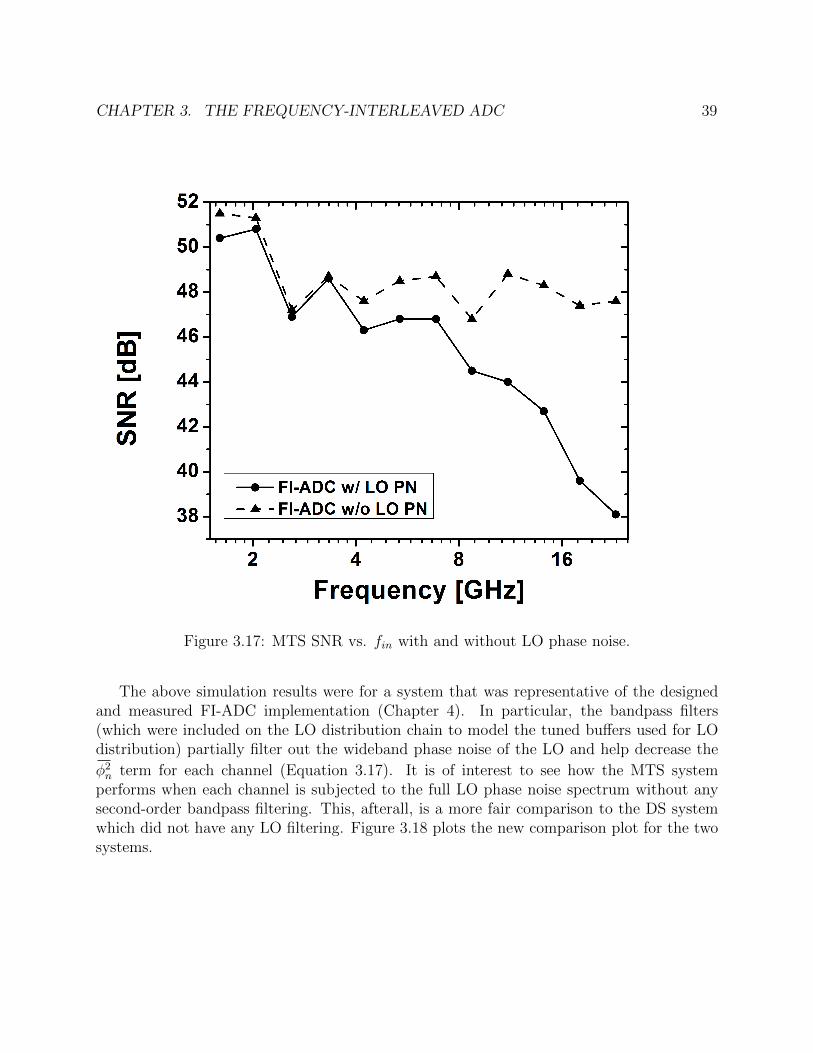
CHAPTER 3. THE FREQUENCY-INTERLEAVED ADC 39
Figure 3.17: MTS SNR vs. fin with and without LO phase noise.
The above simulation results were for a system that was representative of the designedand measured FI-ADC implementation (Chapter 4). In particular, the bandpass filters(which were included on the LO distribution chain to model the tuned buffers used for LOdistribution) partially filter out the wideband phase noise of the LO and help decrease the
φ2n term for each channel (Equation 3.17). It is of interest to see how the MTS system
performs when each channel is subjected to the full LO phase noise spectrum without anysecond-order bandpass filtering. This, afterall, is a more fair comparison to the DS systemwhich did not have any LO filtering. Figure 3.18 plots the new comparison plot for the twosystems.

CHAPTER 3. THE FREQUENCY-INTERLEAVED ADC 40
Figure 3.18: Comparision of SNR vs. fin without LO BPF in the MTS system.
The plots of Figure 3.18 now resemble that of Figure 3.13. Looking at the TI-ADCσj = 200fs plot and the two plots for the FI-ADC, we see the predicted trend of higher
crossover frequency as φ2n is increased (higher σj is equivalent to higher integrated phase
noise). It is also interesting to note that the crossover frequencies for the pair of plots(σj = 200fs and σj = 400fs) are identical.
Now, following the previous discussion of how SNR is dependent on fLO, the plot ofFigure 3.18 begs the question of why isn’t there any frequency dependence exhibited? Theanswer is reciprocal mixing. The wideband phase noise of the LOs in each channel willmix with the input signal regardless of which channel is responsible for processing thatsignal. This wideband phase noise is downconverted to baseband and, if large enough, willbe quantized by the ADC and create a noise spectrum at the output of each of channel. Notethat these channels which don’t process the input signal, should normally be off. Thus, theoutput spectrum will include the input signal tone, the noise of the excited channel and thenoise of all other channels. Because all channels are always contributing to the noise floor of
CHAPTER 3. THE FREQUENCY-INTERLEAVED ADC 41
the output spectrum, the output noise floor is constant and output SNR is independent ofinput frequency. When BPFs were used to model the LO distribution, the far-out widebandphase noise was sufficiently filtered such that only the excited channel and its adjacentchannels contributed to the output noise spectrum. Channels that were further away didn’thave large enough phase noise to “wake-up” their sleeping ADCs since the reciprocal mixingwould occur with the wideband phase noise that was already sufficiently filtered by the BPF.As such, only a subset of channels contribute to the output noise floor and this subset isdependent on the input frequency, leading to the SNR dependence on fLO that was seen inFigure 3.16.
These simulation results show that the answer to the question of which architecture isbetter (TI or FI) isn’t straightforward. In general, the FI architecture has great potentialto outperform the TI architecture at very high input frequencies. Depending on the LOgeneration/distribution (e.g. whether or not BPFs are used), the FI architecture may onlyprovide gains for frequencies which are above the crossover frequency. When this is thecase, the integrated phase noise power introduced during mixing, φ2
n, needs to be minimizedas much as possible in order to make the FI architecture more appealing. Fortunately forthe design presented in Chapter 4, the usage of tuned LO buffers was appropriate (andnecessary). This helps reduce the impact of the wideband phase noise and in turn resultsin the FI architecture outperforming its TI counterpart. In the next chapter, an overviewof practical design considerations for FI-ADCs will be presented along with the design of a25GHz channelized analog front-end (AFE).

42
Chapter 4
Design of a 50 GS/s 6-bit FI-ADC
The target application for this project was pulsed-radar imaging applications [4]. In thesesystems, a pulse-modulated carrier signal is transmitted to a target and the reflected signalis detected. Based on the reflection properties (amplitude and time-of-arrival) measured atvarious carrier frequencies, the dielectric properties of the material can be determined [2]. Inorder to improve the depth resolution of these imagers, smaller pulse-widths must be used.In [3], pulse-widths below 30ps were demonstrated in 0.13µm SiGe technology, resulting inI/Q baseband bandwidths up to 20 GHz. In order sufficiently digitize these bandwidthsfor proper detection, an ADC with an effective sample rate of 50GS/s and 6b resolution isneeded.
This chapter discusses the design of a 50GS/s 6b frequency-interleaved ADC. The focusof the design was on the analog front-end (AFE) which is responsible for the widebanddistribution and channelization of the input signal. However, since the AFE, sub-ADC, anddigital back-end specifications are tightly coupled with one another, a system-level designapproach was initially performed in order to determine the necessary specifications of theAFE.
This chapter begins with a discussion of system-level design considerations. The designof the AFE is then presented, focusing on the circuit design of key building blocks.
4.1 System-Level Design
Number of Channels
The first key design parameter in the FI-ADC is the number of channels, as it has a directimpact on every design block in the system. For example, a larger number of channels resultsin a smaller processing bandwidth per channel which means the sub-ADCs can sample atmuch lower rates and be designed to be very energy-efficient. In addition, the low-pass filtercutoff frequencies are reduced, which can greatly reduce design complexity. On the otherhand, a larger number of channels increases the amount of channels requiring harmoinc

CHAPTER 4. DESIGN OF A 50 GS/S 6-BIT FI-ADC 43
Pros ConsWideband Distr. - Lower BW due to higher capac-
itive loadingMixer - More channels require HRMs
- Larger # of harmonics need tobe cancelled
LPF - Lower corner frequency- Feasibility of higher-order filters
Sub-ADC - Lower sampling rate.- More energy-efficient- Easier to oversample
LO Gen. - Larger # of LO frequencies togenerate/distribute
DSP - Lower data rate on each path- Reduced FIR filter complexity
- Larger # of input datapaths- Larger # of channels to calibrate
Table 4.1: Pros and Cons for larger number of channels.
rejection mixers, as discussed in Chapter 3, adding to design complexity. Furthermore, thewideband distribution becomes more difficult due to the increase in capacitive loading thatneeds to be driven. Table 4.1 summarizes some of the major design parameters impacted.
Assuming power consumption is to be minimized, determining the true optimal numberof channels requires accurate modeling of all the blocks in the design as well as a modeling ofhow the design parameters of each block are coupled. In order to avoid this arduous task, amore heuristic approach was taken. There are a few observations considered in this huerisiticdecision process:
1. The replicated sub-blocks (sub-ADC and LPF) should operate at frequencies far enoughfrom the fT of the process such that the power vs. frequency trade-off is linear ratherthan exponential. Once in this linear tradeoff region, further increase in the numberof channels does not result in as much power savings since the component count mayalso increase linearly, resulting in zero power savings, yet added system complexity.
2. Op-Amp RC filters are limited to practical corner frequencies of 100s of MHz. OtherLPF topologies (gm-C, current-mode) are limited to frequencies below 10GHz in theprocess of interest.
3. There is an upper-limit to the number of stages in the DA due to losses on the trans-mission line. Larger number of stages leads to longer T-lines and hence, increasedlosses. This added loss can overtake the gain being added by the additional stages,resulting in no increase in DA gain and a waste of power [33].

CHAPTER 4. DESIGN OF A 50 GS/S 6-BIT FI-ADC 44
4. Distributing LOs is a significant challenge in regards to the area needed for routingand the coupling due to proximity of the traces. As such, it is desirable to minimizethe number of LOs needed to generated/routed.
Taking these points into consideration, it is best to minimize the number of channels used tothe point where the sub-ADCs are energy-efficient ( < 75fJ/conv-step) and the LPF cornerfrequencies are no more than a few GHz. As such, a 9-channel (1 baseband, 8 passband)architecture was chosen. Each of the passband channels process a bandwidth of 3GHz whichresults in baseband I/Q bandwidths of 1.5GHz. The baseband channel processes frequenciesfrom DC-1.5GHz. The LO frequencies that need to be generated are 3, 6, 9, 12, 15, 18, 21,and 24GHz. Figure 4.1 depicts the processing bandwidths of each channel.
Figure 4.1: Processing bands for each channel.
Channel Filtering - Analog vs. Digital
Adequate filtering is an integral part of the FI-ADC. In [5][16][18][19], the analog filtersare responsible for channelizing the input signal. These filters are designed to precisely deter-mine the edge frequencies of each channel. Due to process variations, the edge frequencies ofthe analog filters will deviate from their ideal values. This causes complications in the designof the digital synthesis filters used for reconstruction since they require apriori knowledge ofthe response of the analog filters [5][34].
In order to relax the system’s sensitivity to the analog filters in the front-end, the jobof setting channel bandwidth is transferred to digital filters. Figure 4.2 shows the proposeddigital backend architecture which is a slightly modified version of Figure 3.2. In this ar-chitecture, the LPFs in the AFE perform the first level of filtering, however their cornerfrequencies are set to be slightly larger than the processing bandwidth of each channel. Forexample, the baseband processing bandwidth is 1.5GHz while the LPF corner frequencywould be set to ∼ 3GHz. Thus, in the AFE, each channel will handle signals from the lower
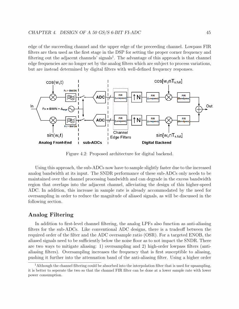
CHAPTER 4. DESIGN OF A 50 GS/S 6-BIT FI-ADC 45
edge of the succeeding channel and the upper edge of the preceeding channel. Lowpass FIRfilters are then used as the first stage in the DSP for setting the proper corner frequency andfiltering out the adjacent channels’ signals1. The advantage of this approach is that channeledge frequencies are no longer set by the analog filters which are subject to process variations,but are instead determined by digital filters with well-defined frequency responses.
Figure 4.2: Proposed architecture for digital backend.
Using this approach, the sub-ADCs now have to sample slightly faster due to the increasedanalog bandwidth at its input. The SNDR performance of these sub-ADCs only needs to bemaintained over the channel processing bandwidth and can degrade in the excess bandwidthregion that overlaps into the adjacent channel, alleviating the design of this higher-speedADC. In addition, this increase in sample rate is already accommodated by the need foroversampling in order to reduce the magnitude of aliased signals, as will be discussed in thefollowing section.
Analog Filtering
In addition to first-level channel filtering, the analog LPFs also function as anti-aliasingfilters for the sub-ADCs. Like conventional ADC designs, there is a tradeoff between therequired order of the filter and the ADC oversample ratio (OSR). For a targeted ENOB, thealiased signals need to be sufficiently below the noise floor as to not impact the SNDR. Thereare two ways to mitigate aliasing: 1) oversampling and 2) high-order lowpass filters (anti-aliasing filters). Oversampling increases the frequency that is first susceptible to aliasing,pushing it further into the attenuation band of the anti-aliasing filter. Using a higher order
1Although the channel filtering could be absorbed into the interpolation filter that is used for upsampling,it is better to seperate the two so that the channel FIR filter can be done at a lower sample rate with lowerpower consumption.

CHAPTER 4. DESIGN OF A 50 GS/S 6-BIT FI-ADC 46
filter provides larger attenuation at aliasing frequencies due to the sharper rolloff of the filter.Figure 4.3 illustrates the tradeoff.
Figure 4.3: Tradeoff between filter rolloff and oversampling ratio.
Generally, there is a practical limit to the order of baseband analog filters, with 5th or6th order being an upper-limit. Given this upper-limit, the attenuation provided by thefilter is fixed, and the only way to further reduce the magnitude of aliased signals is throughoversampling. Table 4.2 shows the required sample rates of the sub-ADCs for various targetedENOBs and filter types with a filter bandwidth of 2GHz. The specification is that all aliasedsignals are at least 3dB below the quantization noise floor (e.g. 5b ENOB is equivalent to anSNDR of 5 ∗ 6.02 + 1.76 = 32dB, so the aliased signals are all 35dB below the signal level).
The three filter types shown in Table 4.2 are chosen for their superior in-band phaseand group delay response. In-band group-delay variation needs to be minimized in orderto reduce dispersive effects. This is important in pulsed-radar applications where the pulse-width determines the depth resolution [2]. Dispersion in the medium and/or the receivercauses a widening of the received pulse, thereby reducing the effective depth-resolution ofthe imager. In addition, the group delay and amplitude of all channels should also match forthe case of a wideband signal that is processed by multiple channels. Thus, it is desirableto have a filter that requires a minimal amount of calibration for equalizing the group delayand amplitude response across all channels.
The Bessel filter is known for its maximally flat group delay, yielding the best responseof all filter types. Unfortunately, this comes at the price of very poor rolloff characteristicsand thus, poor out-of-band attenuation. As a result, the uasge of Bessel filters requires veryhigh oversampling ratios to meet the resolution specifications.
The Butterworth filter provides a maximally flat amplitude response, which is good forminimizing amplitude calibrations. It also provides better rolloff when compared to theBessel filter, but is still gradual when compared to its Chebyshev (I/II) counterparts. Asseen from Table 4.2, a 6th order Butterworth filter would still need to be paired with a 8+GS/s

CHAPTER 4. DESIGN OF A 50 GS/S 6-BIT FI-ADC 47
Bessel Butterworth Inverse-Chebyshev4th 5th 6th 4th 5th 6th 4th 5th 6th
5 bits 14 12 11.4 9.4 8.5 7.6 7.6 6 5.46 bits 16.6 14 13 11.4 9.4 8.4 8.8 6.6 67 bits 19.5 16 14.6 13 10.6 9.4 10.6 7.4 6.48 bits 22.8 19 16.6 16 12.2 10.4 12.2 8.4 7.1
Table 4.2: Sub-ADC sample rate (in GS/s) vs. Filter order/type.
ADC for a 6b system. ADCs operating at this sample rate have reported efficiencies largerthan 100fJ/conv-step [8], which is above the targeted efficiency.
The Inverse-Chebyshev (Chebyshev-II) filter provides an adequate solution to both prob-lems – it provides the sharp rolloff known to the Chebyshev family of filters while maintaininggood in-band performance. The group delay of these filters exhibit no ripples in the pass-band (good for equalization), and can yield a sufficiently flat delay response if the cornerfrequency is set to be appropriately higher than the max frequency of interest. In addition,the magnitude response of the inverse-Chebyshev filter is flat within the passband. As seenin Table 4.2, using a 6th order inverse-Chebyshev filter drops the required ADC sample rateto 6GS/s for a 6b system. ADCs with FOM less than 100fJ/conv-step have been reportedat this sample rate [8].
Analog Front-End Specifications
The first step towards the design of a full 50GS/s, 6b FI-ADC system is the design of theanalog front-end. The AFE is responsible for the wideband distribution and channelizationof the input signal. Given the previous discussions, a 9-channel front-end architecture waschosen. The targeted input bandwidth is 25GHz. The processing bandwidth of each passbandchannel is 3GHz resulting in I/Q baseband processing bandwidths of 1.5GHz. The actualbandwidth of the I/Q baseband is designed to be 2GHz in order to reduce sensitivity toanalog filter variations, while digital FIR filters are used to enforce the 1.5GHz channelcorner frequency.
In order to meet the SNDR requirements for a 6b system, the noise and distortion powerintroduced by the AFE must fall 38 dB below the maximum input signal level. The maindistortion products of interest are caused by 2nd and 3rd order intermodulation products(IM2/3) and harmonic folding. As a result, we require2 IM2/3 < −40dB and HRR > 40dB.To meet the noise specifications, the required noise figure of the AFE can be calculated usinglink budget equations similar to wireless receivers.
For the 6b FI-ADC, the maximum input power, Pi,max, is the input power that yieldsIM2/3 levels equal to the threshold specification (40dB in this example). Assuming that IM3
2Additional margin should be added to these specifications so that the combined power of these undesiredsignals is 38 dB below the input power.

CHAPTER 4. DESIGN OF A 50 GS/S 6-BIT FI-ADC 48
is the dominant distortion, this means that Pi,max can be written in terms of the IIP3 of thereceiver:
Pi,max = IIP3 − 20dB (4.1)
Equation 4.1 is derived from the 2 dB/dB relation between IM3 and input power. OncePi,max is determined, the noise figure of the AFE must be sufficient to yield a minimumdetectable signal (MDS) that is lower than Pi,max.
PMDS < Pi,max (4.2)
PMDS is the minimum input signal power that yields the required SNR at the sub-ADCinput. This constraint can be written using the link budget equation:
SNRADC = SNRIN −NFAFE (4.3a)
SNRADC = PMDS + 174dBm− 10 · log(BW )−NFAFE (4.3b)
where SNRADC is the required SNR at the output of the AFE, BW is the channel processingbandwidth, and NFAFE is the noise figure of the AFE. Solving for PMDS and plugging inSNRADC = 38dB and BW = 1.5GHz, we get:
PMDS = SNRADC − 174dBm + 10 · log(1.5e9) +NFAFE (4.4a)
PMDS = 38dB− 174dBm + 92dB +NFAFE (4.4b)
PMDS = −44dBm +NFAFE (4.4c)
Using Equations (4.1), (4.2), and (4.4c), we arrive at a relation between IIP3 and NFAFE:
NFAFE < IIP3 − (−24dBm) (4.5)
Equation 4.5 sets an upper bound on the noise figure of the AFE, given its IIP3 perfor-mance. The first observation is that it immediately sets a lower bound on the IIP3 of theAFE since NF of any receiver must be greater than 0dB. Assuming a practical lower boundon NF of 4dB, the lower bound on IIP3 becomes:
IIP3 > −20dBm (4.6)
This lower bound can be easily met, but it should be noted that it can become more con-straining for higher resolution systems (larger SNRADC) and/or implementations with afewer number of channels (larger channel processing bandwidth, BW ). Another observationfrom Equation 4.5 is that a more linear front-end relaxes the noise performance requirement.This provides another handle for optimizing the AFE design - by maximizing the linearityof the linearity-limiting block (the mixer in this design), the required gain of the front-end

CHAPTER 4. DESIGN OF A 50 GS/S 6-BIT FI-ADC 49
DA can be reduced. Since the DA runs from a higher supply voltage, power can be saved.In addition, the lower gain required from the DA can yield increased DA bandwidth.
At this point, it becomes apparent that Equations (4.5) and (4.6) drive the design method-ology for the AFE, as will be discussed in the following section.

CHAPTER 4. DESIGN OF A 50 GS/S 6-BIT FI-ADC 50
4.2 AFE Circuit Design
The first phase of this design focused on the analog front-end. The AFE consists of thedistributed amplifier, harmonic rejection mixers, lowpass filter, and 8-frequency LO genera-tion. Figure 4.4 shows the block diagram of the AFE architecture that was designed. Theinput signal is applied to a distributed amplifier that provides front-end gain and widebanddistribution to the various channels. Each stage of the DA is tapped by a single channelwhich contains a transconductor, passive mixer and lowpass filter. Channels 2 and 3 utilizeharmonic rejection mixers since the harmonics of their LO frequencies fall within the inputbandwidth.
The following sections discuss the designs of each of the building blocks shown in Fig-ure 4.4. The first block that was designed was the high-frequency harmonic rejection mixer.The mixer dominates the linearity performance of the AFE. Once the linearity and NF ofthe mixer was optimized, the required gain of the distributed amplifier was calculated to setan appropriate NFAFE in accordance with Equation 4.5.
Figure 4.4: FI-ADC AFE Block Diagram.

CHAPTER 4. DESIGN OF A 50 GS/S 6-BIT FI-ADC 51
Figure 4.5: Conventional method for harmonic rejection.
Wideband Harmonic Rejection Mixer
Chapter 3 discussed the harmonic folding problem. In this design, channels 2 and 3are susceptible to harmonic folding. For channel 2, the 3rd, 5th, and 7th harmonics of its3GHz LO all fall within the 25GHz input bandwidth and can downconvert signals thatare out of its processing bandwidth. For channel 3, only the 3rd harmonic of its 6GHzLO falls within the input bandwidth. Due to the high LO frequencies (3GHz and 6GHz),conventional harmonic rejection techniques cannot be easily adopted. In the conventionalHRM architecture, complex digital logic is used to generate various non-overlapping clockphases. These clock signals then feed the gain-weighted mixing paths whose outputs aresummed. This process emulates multiplication by a sampled-and-held sinusoid (SHS) whichhas reduced harmonic content (Figure 4.5). Designing the digital logic to run at thesefrequencies is challenging and can consume considerable amounts of power. As an example,in [26], a clock of N ·LO was needed in order to achieve harmonic rejection for harmonics upto (N -1). In our system, for 3rd and 5th harmonic rejection in Channel 2, we would need torun the digital logic at 18GHz, which is not practical at this technology node. Thus, thereis a need for a high-frequency HRM architecture that is capable of obtaining greater than40dB of HRR.
Figure 4.6 shows the schematic of the proposed high-frequency HRM that was introducedin Chapter 3. The main and auxiliary mixers each contain identically-sized passive switchingquads. Independent gm-stages are used to generate the AC current inputs to each switching

CHAPTER 4. DESIGN OF A 50 GS/S 6-BIT FI-ADC 52
quad3. Identically-sized switching quads are used for improved matching of the gain ratiobetween the two paths. The gain ratio is set by the strengths of the gm-stages.
Figure 4.6: Schematic of proposed HRM.
An alternative implementation is shown in Figure 4.7. In this implementation, the gainratio is achieved through relative sizing of the switching quads. Although this architectureoffers superior linearity performance (elimination of transconductor stage), it has a fewdisadvantages when it comes to setting relative gains. First, it is difficult to set the gainratio since the effective gain of each path isn’t solely determined by the ratio of device sizes– parasitic source/drain capacitance and rise/fall time of the LO each change the effectiveimpedances of the switching paths. For instance, with matched rise/fall times at the inputof each quad, the rise/fall time observed on the output current waveforms would be differentdue to the different time constants of each path. By using identical paths, we can eliminatethis second-order impact on the gain.
Figure 4.8(a) shows how the attainable HRR is limited by these second-order effects ascompared to the identical switching quad topology. The figure shows a plot of the attainableHRR of each topology as a function of the rise/fall time. The rise/fall times at the inputof each switching quad are matched for these simulations. As illustrated in the plot, theidentical path topology can achieve 20dB larger HRR, on average, than the alternativedesign. Furthermore, the identical path topology shows very low sensitivity to the inputrise/fall times, unlike the alternative design which has a HRR that sharply drops as rise/falltimes are increased.
3The gm-stages are AC coupled to the mixing quad, as illustrated in Figure 4.4. The current sources inFigure 4.6 only represent an AC signal.

CHAPTER 4. DESIGN OF A 50 GS/S 6-BIT FI-ADC 53
Figure 4.7: Alternative schematic for HRM.
Figure 4.8: Performance comparison of two HRM topologies.

CHAPTER 4. DESIGN OF A 50 GS/S 6-BIT FI-ADC 54
These trends can be explained by Figure 4.8(b) which shows the magnitudes of theharmonic components of interest for the main and auxiliary mixers. For proper harmonicrejection to take place, we require that the magnitude of the 3rd harmonic of the main mixermatch the fundamental of the auxiliary mixer. As illustrated in the plot, perfect matchingbetween the two paths is difficult to achieve through device sizing in the alternative approach4
and causes the attainable HRR to be 20dB lower, on average. Secondly, the magnitudes in theidentical path topology exhibit similar behavior as a function of rise/fall time, explainingthe previously noted insensitivity. The magnitudes in the alternative topology, however,exhbit poor matching which worsens for increasing rise/fall times. This is because the non-identical paths exhibit non-identical behaviors as rise/fall time is increased and this causesthe attainable HRR to continually degrade.
The other critical advantage of including a gm stage that preceeds the mixing quad isthe flexibility to tune the gain of the paths in the presence of process variation. Montecarlosimulations show a mean HRR of 36dB, which means tuning needs to be incorporated inorder obtain harmonic rejection levels greater than 40dB. Having a gm stage provides adirect handle on the gain of each path which can be tuned via the tail current source. Ahigh-resolution current DAC can then be used as the tail source in order to achieve theappropriate gain resolution to meet the HRR specification. In the alternative approach,device size would have to be tuned by switching in/out minimum width devices. Since amaximum device width is usually set for keeping the power of the LO driver reasonable,minimum-sized finger widths would likely have to be used in order to obtain the desiredresolution. This can lead to a difficult design since large series switches will also be neededin conjunction with the minimum-width devices.
Figure 4.9 shows a schematic of the gm-stage used in the HRM. Two auxiliary stages areused for driving the auxiliary mixers for 3rd and 5th harmonic rejection5. An active-load isutilized to increase the output impedance of the gm stage and increase the conversion gainby forcing the signal current to flow into the low-impedance node at the input of the lowpassfilter. Since the mixer and lowpass filter chain is operating in current-mode, the signal swingat the output node of the gm stage is small and the common-mode voltage is a (relatively)free parameter that can also be used for optimizing noise/linearity performance. A common-mode feedback (CMFB) amplifier is used to drive the gates of the PMOS active-loads andset the common-mode output voltage. The output common-mode voltage is made tunableby using a votlage DAC to the feed the reference voltage of the CMFB amplifier.
4For the alternative topology, the ratio of device sizes was set to yield the maximum HRR at a singlerise/fall time of 20ps. These devices sizes were then used for the various simulation sweeps.
5Although channel 2 requires 7th harmonic rejection, it was not implemented in this design

CHAPTER 4. DESIGN OF A 50 GS/S 6-BIT FI-ADC 55
Figure 4.9: Schematic of HRM gm stage.
Rise/Fall Time Impact on Phase
Once the gain ratios have been appropriately set, the next limiting factor in attainableHRR is the phase match between the two paths. Phase mismatch is primarily caused bynon-identical routing on the RF, IF, and LO paths. However, even if very careful layouttechniques were used to make all routes nearly identical, there is still another mechanismwhich limits the attainable HRR – matching of the rise/fall time at the inputs of the mainand auxiliary mixers. In the previous simulations (Figure 4.8), the main and auxiliaryrise/fall times were set equal. However, as can be seen in Figure 4.10, the attainable HRRis also sensitive to the matching of the respective rise/fall times at the input of the mainand auxiliary mixers, tr,main and tr,aux. In the plot, erise is the percentage error betweentr,main and tr,aux (erise =
tr,main−tr,auxtr,main
). The rise time and fall time are equal for each mixer
(trise = tfall), and have a nominal value of 30ps. The fundamental LO frequency is 4GHz.The overall sensitivity of the attainable HRR to rise/fall time mismatch can be explained
using Fourier analysis. The Fourier series for a square wave with amplitude A, period T ,and non-zero rise/fall time, tr, is given by [35]:
Cn∠θn = A ·sin(nπ2
)nπ2
·sin(nπtrT
)nπtrT
∠− nπ
2− nπtr
T(4.7)
The first sinc expression in Equation 4.7 has values of 2π· [1, 1
3, 1
5, 1
7, ...], which are the well
known coefficients for a perfect square with zero rise/fall time. The second sinc expressioncaptures the impact that non-zero rise/fall times have on the amplitudes of the fouriercoefficients. This sinc shaping of the amplitude as a function of tr was exhibited in the plotsof Figure 4.8(b). Assuming waveforms that have sharp transitions compared to the periodof the harmonic (tr T
n), we can write nπtr T and note that sin(x) ≈ x for x 1. This
sets the second sinc function to unity, and Equation 4.7 simplifies to:
Cn∠θn = A ·sin(nπ2
)nπ2
∠− nπ
2− nπtr
T(4.8)

CHAPTER 4. DESIGN OF A 50 GS/S 6-BIT FI-ADC 56
Figure 4.10: Simulated HRR vs. rise/fall time mismatch between main and aux. mixers.
This says the the primary manner in which a mismatch in rise/fall times limits the attainableHRR is by introducing additonal phase shift. Note that the harmonic of interest for the mainmixer is the 3rd harmonic (n = 3), while the harmonic of interest for the auxiliary mixer isthe 1st harmonic (n = 1). In both cases, n
Tevaluates to the same value since the auxiliary
mixer is driven by 3·LO (Tmain = 3·Taux, where Tmain and Taux represent the LO period usedin Equation 4.8 for the main mixer and auxiliary mixer, respectively). Thus, both harmonicsof interest will experience the same phase shift if tr,main = tr,aux, resulting in proper harmoniccancellation.
Using Equation 4.8, we can plot the theoretical HRR that results from the phase errorintroduced when tr,main 6= tr,aux as shown in Figure 4.11. In this figure, the attainable HRR isplotted as function of erise for Tmain = 1ns (fLO = 1GHz) and Tmain = 250ps (fLO = 4GHz).The simulated HRR values from Figure 4.10 are also included for comparison. As seenin Figure 4.11, higher sensitivity to rise/fall time mismatch is exhibited by the higher LOfundamental frequency. This is predicted by Equation 4.8 – higher LO frequencies (smallerTmain) lead to larger values for n
Tand thus a larger phase shift for a given ∆tr. Lastly,
Figure 4.11 shows that the phase shift is the dominant non-ideality introduced when tr,main 6=tr,aux, as opposed to the amplitude attenuation dictated by the second sinc expression inEquation 4.7. This is exhibited by the close matching between the simulated HRR and the

CHAPTER 4. DESIGN OF A 50 GS/S 6-BIT FI-ADC 57
HRR predicted by Equation 4.8, which only takes phase shift into account.
Figure 4.11: HRR vs. erise as predicted by Equation 4.8.
Figure 4.12 further illustrates how the phase error introduced when tr,main 6= tr,aux isthe dominant limitation of attainable HRR. For +/ − 15% error, the max amplitude errorintroduced is 1.6% while the phase error introduced is +/− 10. These errors independentlytranslate into max attainable HRRs of 45.5dBand 24.7dB, respectively. Thus, the phaseerror introduced must be accounted for6 by using calibration.
In order to calibrate the phase matching of the main and auxiliary paths of the HRM,I/Q phase interpolators [36] are placed on the LO path to the auxiliary mixers as shown inFigure 4.4. A 9b differential current DAC is used for the tail sources of the phase interpolatorsin order to achieve sufficient resolution over the entire 360 range. With proper tuning, thesimulated 3rd and 5th HRRs exceed 40 and 45dB, respectively. The simulated IIP3 of theHRM was +11dBm. The worst-case NF occurs for the HRM used in channel 2 which utilizestwo auxiliary paths (3rd and 5th harmonic rejection) and is equal to 19dB. The simulatedNF for the mixer used in channels 4-9 (main mixer only) was 17dB.
6In addition to the phase mismatch caused by non-identical routing.

CHAPTER 4. DESIGN OF A 50 GS/S 6-BIT FI-ADC 58
Figure 4.12: Magnitude and phase error caused when tr,main 6= tr,aux (fLO = 4GHz).
Multi-Tap Distributed Amplifier
The distributed amplifier (DA) enables wideband signal distribution to the nine channelsby absorbing the input capacitance of the channels into the drain transmission line (T-line).A simplified schematic of the 9-stage DA was shown in Figure 4.4. Figure 4.13 shows amore detailed schematic of the DA. In the implemented DA, each gain stage is comprised ofa cascoded common-source amplifier for improved stability and reduced resistive loading ofthe drain T-line. The input of the gain stage is capacitively coupled to the gate T-line. Ineach stage, a diode-connected mirror device provides dc biasing. The T-lines are formed bydiscrete inductors and the loading capacitances of each channel and DA gain stage.
Given the noise performance of the HRM, the acceptable gain of the DA was calculatedusing Equation 4.5 and the cascaded noise factor formula:
FAFE = FDA +FHRM − 1
GDA
(4.9)
where FAFE, FDA, and FHRM are the noise factors of the full AFE, the DA, and the HRM,respectively, and GDA is the power gain of the DA. The IIP3 of the AFE that appears inEquation 4.5 is also dependent on GDA. Since the DA and LPF operate on a 2.4V supply,

CHAPTER 4. DESIGN OF A 50 GS/S 6-BIT FI-ADC 59
Figure 4.13: Schematic of Distributed Amplifier.
we may assume that the mixer is the dominant linearity-limiting block. Thus, the IIP3 ofthe AFE is simply the IIP3 of the mixer, input referred:
IIP3 =IIP3,HRM
GDA
(4.10)
Looking at Equations (4.5), (4.9), and (4.10), we see that there may be a maximum allowableGDA. Starting with GDA = 1, increasing GDA decreases both NFAFE (Equation 4.9) andIIP3 (Equation 4.10) which appear on each side of the inequality in Equation 4.5. As GDA isfuther increased, NFAFE becomes dominated by the noise performance of the DA, as desired,and becomes less dependent on GDA. At this point, any further increase in GDA only lowersIIP3 while NFAFE remains almost constant and equal to the noise figure of the DA. Thismakes it harder to satisfy the inequality in Equation 4.5 and thus, further increasing GDA
is undesirable.Given a targetted DA NF of 6dB, FHRM of 79, IIP3,HRM of +11dBm, and 6b system
resolution, we can see from Figure 4.14 that the inequality of Equation 4.5 is met with largemargin for GDA values below 18dB. In this figure, the righthand side (RHS) and lefthandside (LHS) of the inequality are plotted as a function of GDA for various targeted systemresolutions. According to Equation 4.5, we require that RHS > LHS in order to meetspecifications.

CHAPTER 4. DESIGN OF A 50 GS/S 6-BIT FI-ADC 60
Figure 4.14: Plot of RHS and LHS of Equation 4.5 for various system specifications.
Recall that Equation 4.5 was derived assuming a 6b system. If we were designing an 8bsystem, the maximum value for GDA becomes 15dB.
The implication of Equation 4.6 can be seen by lowering IIP3,HRM to +5dBm for an 8bsystem. As shown in Figure 4.14, there aren’t any sufficient values of GDA that can satisfythe inequality which means that the linearity/noise performance of the AFE is insuffcientfor an 8b system. Thus, maximizing the linearity performance of the mixer is critical whendesigning higher resolution systems.
In order to allow for the AFE to be adapatable for potential usage in an 8b system,we need to set GDA < 15dB. As such, 10dB was the targeted gain for the DA with a NFof 5-6dB. Figures 4.15 and 4.16 show the simulated gain and group delay response of thedesigned DA. Figure 4.15 plots the response exhibited at each tap. The DC gain is 7.8dBand simulated NF is 4dB. The gain is below the targeted 10dB value due to T-line losses. Asseen in the figure, the bandwidths of all taps are not equivalent – earlier taps (taps closestto the source) exhibit lower bandwidths than later taps with the final tap achieving the full24GHz bandwidth. This behavior is explained in more detail in the following section.
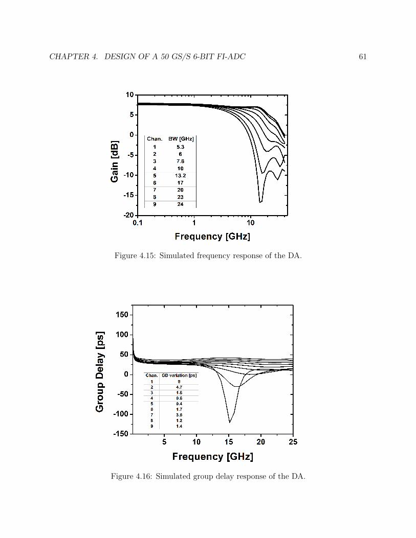
CHAPTER 4. DESIGN OF A 50 GS/S 6-BIT FI-ADC 61
Figure 4.15: Simulated frequency response of the DA.
Figure 4.16: Simulated group delay response of the DA.

CHAPTER 4. DESIGN OF A 50 GS/S 6-BIT FI-ADC 62
Tap Bandwidth
Traditional DAs have a single output taken at the final stage. The forward travelingwave on the gate line is coupled to the drain line via the gain stages. A forward and reversetraveling wave is then generated on the drain line. If the propagation velocities of the gateand drain T-lines are equal, then the forward traveling waves on the drain line add coherently,yielding a voltage gain proportional to the number of stages [33]:
Vo = Zd · Id (4.11a)
= Zd · −gm4vse−(N−1)jθ ·N (4.11b)
where Vo is the voltage at the load, Zd is the load impedance of the drain line which is equal tothe characteristic impedance, Id is the drain current at the load, gm is the transconductanceof each gain stage, vs is the input voltage amplitude, N is number of stages, and θ is thephase delay between each stage7. From Equation 4.11b, we see that the output voltage isproportional to N and gm, while the exponential term captures the phase delay from inputto output.
Equation 4.11b is valid for the last stage of the DA. Unlike the signal at the last stage(load) which is a summation of only forward traveling waves, the signal at each intermediatetap of the DA is a superposition of the forward traveling waves and the reverse travelingwaves created by the latter stages. Due to the varying path lengths, the reverse travelingwave will experience a different phase delay than the forward traveling wave. This createsa low pass filtering effect – the phase difference is larger at higher frequencies (θ ∝ ω) andresults in higher attenuation when summing the forward and reverse waves. This low passfiltering effect is more pronounced for the earlier stages due to the larger number of reversetraveling waves, with successively increasing bandwidth at each tap as you move towardsthe final output.
To illustrate this effect, we can derive the magnitude response at each tap. The totaldrain current at tap m is a summation of the m forward traveling currents created by thegain stages preceeding (and including) that stage and the N − m reverse traveling wavescreated by succceeding gain stages:
Id,m = Id,forward + Id,reverse (4.12a)
=1
2
m∑k=1
id,ke−(m−k)jθ +
1
2
N∑k=m+1
id,ke−(k−m)jθ (4.12b)
where id,k is the drain current contributed by stage k, and is given by:
7Note that θ is proportional to the frequency of the signal, θ ∝ ω.

CHAPTER 4. DESIGN OF A 50 GS/S 6-BIT FI-ADC 63
id,k = −gmvgs,k (4.13a)
= −gmvs2e−(k−1)jθ (4.13b)
where vs is the amplitude of the input signal. Using Equation 4.13b, Id,forward becomes:
Id,forward = −gm4vs
m∑k=1
e−(k−1)jθe−(m−k)jθ (4.14a)
= −gm4vs
m∑k=1
e−(m−1)jθ (4.14b)
= −gm4vse−(m−1)jθ ·m (4.14c)
(4.14d)
and Id,reverse becomes:
Id,reverse = −gm4vs
N∑k=m+1
e−(k−1)jθe−(k−m)jθ (4.15a)
= −gm4vse
(m+1)jθ
N∑k=m+1
e−(2k)jθ (4.15b)
With Equations (4.14d) and (4.15b), Equation (4.12b) now becomes:
Id,m = −gm4vs
[me−(m−1)jθ + e(m+1)jθ
N∑k=m+1
e−(2k)jθ
](4.16a)
= −gm4vse
jθ
[me−mjθ + emjθ
N∑k=m+1
e−(2k)jθ
](4.16b)
The expression in brackets in Equation 4.16b is a complex number that captures the fre-quency dependent amplitude (and additional phase shift). The frequency dependence iscaptured by θ. Thus, we are interested in the magnitude of the expression in brackets. Wecan first simplify the summation term using the identity:
N∑k=0
ejkx =sin(1
2(N + 1)x)
sin(12x)
ejxN/2 (4.17)

CHAPTER 4. DESIGN OF A 50 GS/S 6-BIT FI-ADC 64
The summation in Equation 4.16b can now be written as:
N∑k=m+1
e−(2k)jθ =N∑k=0
e−(2k)jθ −m∑k=0
e−(2k)jθ (4.18a)
=sin((N + 1)θ)
sin(θ)e−jNθ − sin((m+ 1)θ)
sin(θ)e−jmθ (4.18b)
= SNe−jNθ − Sme−jmθ (4.18c)
where SN = sin((N+1)θ)sin(θ)
and Sm = sin((m+1)θ)sin(θ)
. Plugging Equation 4.18c back into Equa-
tion 4.16b, we get (after simplification):
Id,m = −gm4vse−j(m−1)θ
[m+ SNe
−j(N−2m)θ − Smejmθ]
(4.19)
Equation 4.19 is a general formula for the drain current at any given tap in the DA. Wecan verify that it agrees with the traditional formula by plugging in m = N :
Id,N = −gm4vse−j(N−1)θ
[N + SNe
−j(N−2N)θ − SNejNθ]
(4.20a)
= −gm4vse−j(N−1)θ
[N + SNe
jNθ − SNejNθ]
(4.20b)
= −gm4vse−j(N−1)θ ·N (4.20c)
which agrees with the formula for drain current at the load that was given in Equation 4.11b.We can now easily identify the real and imaginary parts of the complex number contained
in brackets in Equation 4.19:
<[Id,m] = m+ SN cos ((N − 2m)θ)− Sm cos(mθ) (4.21a)
=[Id,m] = − (SN sin ((N − 2m)θ) + Sm sin(mθ)) (4.21b)
The magnitude response as a function of θ (and hence, frequency) can be written as:
|Id,m| =gm4vs · [(m+ SN cos ((N − 2m)θ)− Sm cos(mθ))2
+ (SN sin ((N − 2m)θ) + Sm sin(mθ))2]12 (4.22)
Equation 4.22 captures the frequency dependence of the drain current magnitude as af-fected by the summation of forward and reverse traveling waves along a lossless transmissionline. We can plot the magnitude response as a function of frequency by substituting in thelong expression for θ [37][38]:

CHAPTER 4. DESIGN OF A 50 GS/S 6-BIT FI-ADC 65
θ = β · l (4.23a)
= ω√LC · l (4.23b)
where β is the imaginary part of the T-line propogation constant, l is the distance (measuredalong the T-line) between each gain stage, and L and C are the inductance and capacitanceper unit distance, respectively. Figures 4.17 and 4.18 plot the normalized frequency responseaccording to Equation 4.22 and the group delay response as derived from Equations 4.21a and4.21b. The T-line parameters (L, C, l) are chosen to be on the same order as the designedT-line. However, the plots are not meant to model the true responses of the designed DA,but only capture the general behavior.
Figure 4.17: DA frequency response of according to Equation 4.22.
Comparing Figure 4.17 to Figure 4.15, we see that it captures the bandwidth limitationexperienced by earlier stages in the DA. The final stage’s response experiences no atten-tuation (has infinite bandwidth) since there are no reverse traveling waves to destructivelyinterefere with the forward traveling waves. In the real design, this bandwidth is finite andset by the losses of the T-line as well as the cutoff frequency of the synthesized T-line [37][38].

CHAPTER 4. DESIGN OF A 50 GS/S 6-BIT FI-ADC 66
Figure 4.18: DA group delay response of according to Equations 4.21a and 4.21b.
The low-pass frequency response of each tap is a convenient effect as it attenuates out-of-band signals. The only constraint is to make sure that the inherent bandwidth of eachDA tap is greater than or equal to the highest frequency that channel is responsible forprocessing.
Current-Mode LPF
The high-frequency lowpass filter is implemented using a current-mode topology as pre-sented in [39]. The schematic of the lowpass filter is shown in Figure 4.19. As discussedin [39], the input impedance looking up into the drains of M1 and M2 resemble that of aninductor in shunt with a resistor (Figure 4.20). The output current being fed to the loadresistor is the current through the inductor of the equivalent circuit. When combined withthe input capacitor, C1, the transfer function formed from iin to iout is a second-order low-pass filter with two complex-conjugate poles. The lowpass behavior can be understood byobserving Figure 4.20. At DC, the inductor presents ideally zero impedance to the sourceand passes all of the input current to the load. As the frequency is increased, the inductorimpedance increases, creating a less desirable path for the signal current to flow while thecapacitor, C1, shunts increasingly more of the signal current to ground.
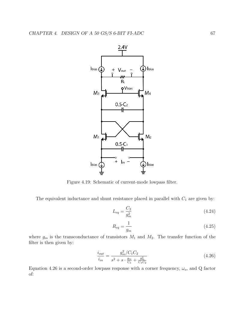
CHAPTER 4. DESIGN OF A 50 GS/S 6-BIT FI-ADC 67
Figure 4.19: Schematic of current-mode lowpass filter.
The equivalent inductance and shunt resistance placed in parallel with C1 are given by:
Leq =C2
g2m
(4.24)
Req =1
gm(4.25)
where gm is the transconductance of transistors M1 and M2. The transfer function of thefilter is then given by:
ioutiin
=g2m/C1C2
s2 + s · gmC1
+ g2m
C1C2
(4.26)
Equation 4.26 is a second-order lowpass response with a corner frequency, ωo, and Q factorof:

CHAPTER 4. DESIGN OF A 50 GS/S 6-BIT FI-ADC 68
Figure 4.20: Equivalent circuit for current-mode lowpass filter.
ωo =gm√C1C2
(4.27)
Q =
√C1
C2
(4.28)
Equations (4.27) and (4.28), are two equations with three unknowns. With the addition ofone more constraint, there is enough information to perform the design of the filter. The lastconstraint is derived from the desire to maximize the conversion gain of the entire AFE. Themaximum input impedance of the filter is 1
gmand occurs at ωo [39]. This input impedance
needs to be much smaller than the output impedance of the HRM in order to draw all of thesignal current into the filter. The caveat is that we would like to do this within a reasonablepower budget since the AFE will have 17 instances of the lowpass filter. Given this, 1
gmwas
set to 100Ω. This value yielded acceptable tradeoff between the degradation in the AFEconversion gain and the power consumption of the LPF. The filter quality factor was set toQ ≈ 2 since low Q poles yield improved group delay response (e.g. Bessel filters) and theminimum allowable Q is 1
2in order to guranatee complex conjugate poles.
The corner frequency of the LPF was designed to be larger than the channel processingbandwidth for improved in-band group delay and noise performance. The simulated magni-tude, group delay, and noise responses are shown in Figures 4.21, 4.22 and 4.23, respectively.The filter has a cutoff frequency of 4.5GHz and exhbits less than 2ps of group delay varia-tion within the 1.5GHz bandwidth. The noise response exhbits the behavior predicted by[39]. The excessive bandwidth of the filter was needed to push the noise bump exhibitedin Figure 4.23 far enough out so as to not affect the in-band noise performance; due to thelack of excessive front-end gain, the noise performance of latter blocks has a non-negligibleimpact on the noise figure of the AFE.
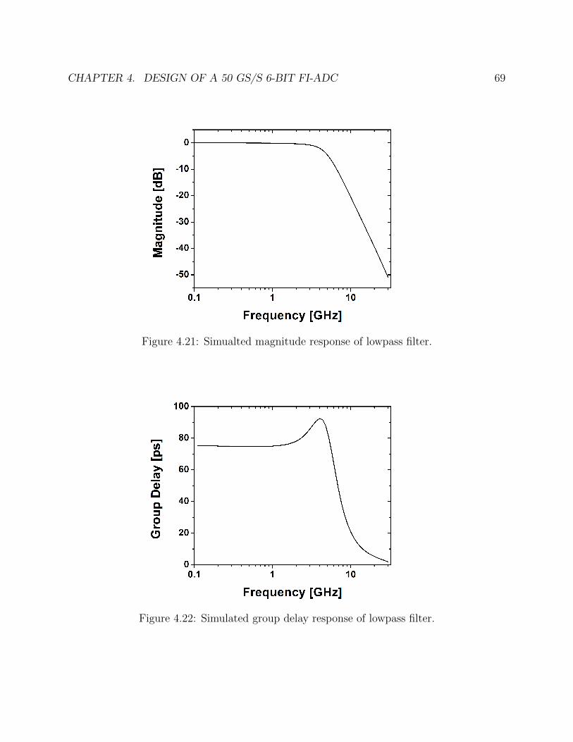
CHAPTER 4. DESIGN OF A 50 GS/S 6-BIT FI-ADC 69
Figure 4.21: Simualted magnitude response of lowpass filter.
Figure 4.22: Simulated group delay response of lowpass filter.

CHAPTER 4. DESIGN OF A 50 GS/S 6-BIT FI-ADC 70
Figure 4.23: Noise response lowpass filter.
For this design, the lowpass filter was included in order to perform wideband current-to-voltage conversion for driving the 50Ω output buffers while also providing some level ofattenuation of out-of-band signals. Proper filtering in the analog domain is handled by off-chip filters that precede the sub-ADCs, making the DA, harmonic rejction mixers, and LOgeneration/distribution, the focus of the design.
LO Generation
In order to provide the eight LO frequencies needed for downconversion and harmonicrejection, two chains of frequency dividers are used (Figure 4.4). The first chain is drivenby a 48 GHz input, and generates the 24, 12, 6, and 3GHz LOs. The second chain is drivenby a 36GHz input, and generates 18 and 9GHz. SSB mixing is performed between the3 and 18 GHz LOs to generate 15 and 21GHz. CML latch-based dividers are utilized toperform frequency division at high frequencies [40]. Figure 4.24 shows a schematic of theCML dividers.
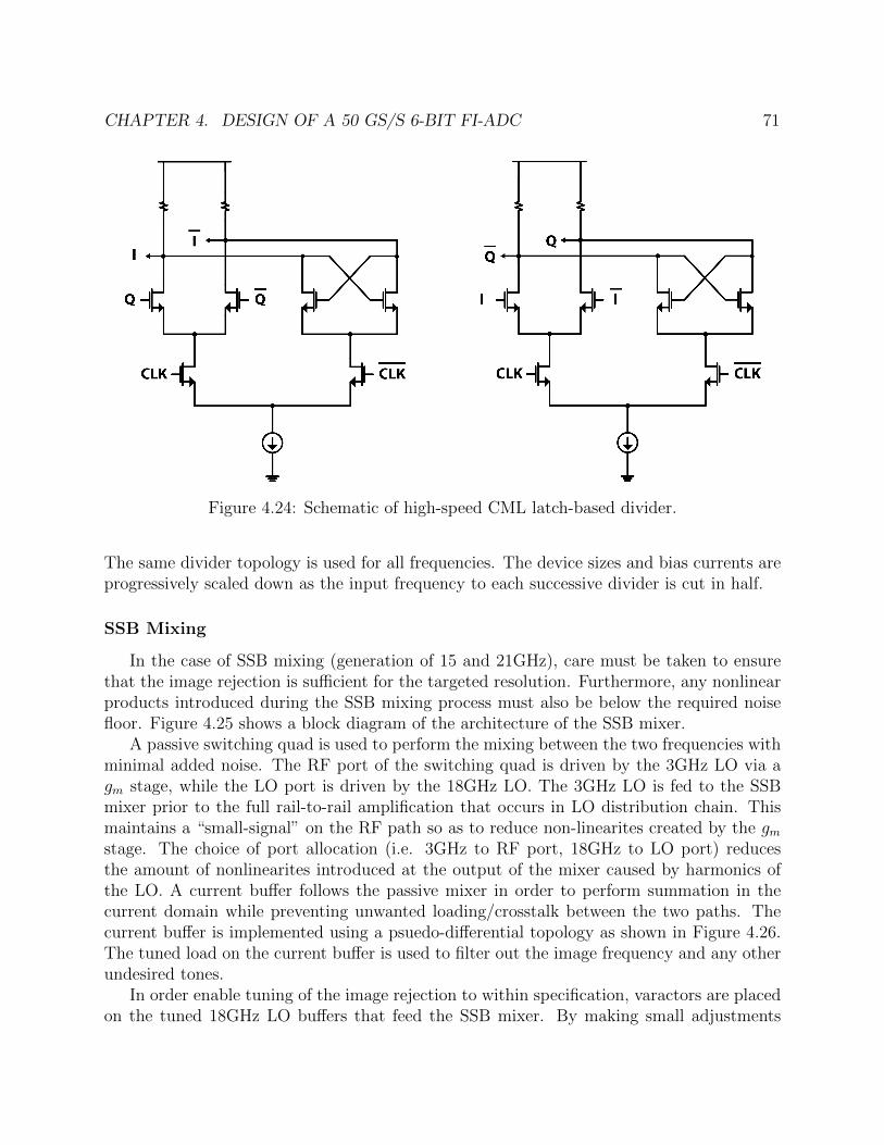
CHAPTER 4. DESIGN OF A 50 GS/S 6-BIT FI-ADC 71
Figure 4.24: Schematic of high-speed CML latch-based divider.
The same divider topology is used for all frequencies. The device sizes and bias currents areprogressively scaled down as the input frequency to each successive divider is cut in half.
SSB Mixing
In the case of SSB mixing (generation of 15 and 21GHz), care must be taken to ensurethat the image rejection is sufficient for the targeted resolution. Furthermore, any nonlinearproducts introduced during the SSB mixing process must also be below the required noisefloor. Figure 4.25 shows a block diagram of the architecture of the SSB mixer.
A passive switching quad is used to perform the mixing between the two frequencies withminimal added noise. The RF port of the switching quad is driven by the 3GHz LO via agm stage, while the LO port is driven by the 18GHz LO. The 3GHz LO is fed to the SSBmixer prior to the full rail-to-rail amplification that occurs in LO distribution chain. Thismaintains a “small-signal” on the RF path so as to reduce non-linearites created by the gmstage. The choice of port allocation (i.e. 3GHz to RF port, 18GHz to LO port) reducesthe amount of nonlinearites introduced at the output of the mixer caused by harmonics ofthe LO. A current buffer follows the passive mixer in order to perform summation in thecurrent domain while preventing unwanted loading/crosstalk between the two paths. Thecurrent buffer is implemented using a psuedo-differential topology as shown in Figure 4.26.The tuned load on the current buffer is used to filter out the image frequency and any otherundesired tones.
In order enable tuning of the image rejection to within specification, varactors are placedon the tuned 18GHz LO buffers that feed the SSB mixer. By making small adjustments

CHAPTER 4. DESIGN OF A 50 GS/S 6-BIT FI-ADC 72
Figure 4.25: Architecture used for SSB mixing.
to the resonant frequency of the tank, varactors can introduce sufficient phase shift on the18GHz LO path while maintaing sufficient LO amplitude to drive the passive switching quad.The varactor is tuned using a 4b voltage DAC. In addition, the gain of the gm stage is alsotunable via a programmable tail current.
LO Buffering/Distribution
The passive switching quad of the AFE downconversion mixers require large amplitudeLO signals for sufficient conversion gain and noise performance. In order to avoid significantdegradation in mixer gain and noise figure, a 0.8 − 1Vpp signal needs to delivered to theLO port of the mixer. Given the 200− 300mVpp swing at the output of the CML dividers,LO buffers are utilized to amplify the LO signals to the appropriate level. For the highLO frequencies (12GHz and above), a two-stage buffering approach is used. The first stage,referred to as the PreAmp, is an intermediary buffer between the CML divider and the

CHAPTER 4. DESIGN OF A 50 GS/S 6-BIT FI-ADC 73
Figure 4.26: Current buffer for SSB mixer.
main LO driver, and presents a minimal amount of capacitive loading to the high-frequencydividers while providing a gain of ∼ 2. The second stage is the LO driver which amplifies thesignal to the full 1Vpp nominal swing and drives the 100fF capacitive load presented by thepassive mixer quad in addition to the parasitic capcitance associated with the routing. Forthe lower LO frequencies (9GHz and below), a static CMOS inverter chain is used as shownin Figure 4.27. The output of the CML dividers are AC-coupled to the first stage of self-biased inverters. The resistive feedback places the input and output bias points at mid-railand the pMOS and nMOS are sized such that the threshold voltage, VM , of the inverter isalso equal to the mid-rail voltage. This yields maximum sensitivity and minimal duty-cycledistortion when performing the level conversion. Differential signaling is reinforced by usingweak cross-coupled inverters across the two single-ended paths.
A majority of the LO distribution routes have lengths greater than 500µm. As a result,the routing capacitance is very significant. To make matters worse, high-frequency channelsare subject to transmission-line effects which transform the load capacitance to a larger valuedependent on the length of the line [37]. A differential transmission line (Zo,d = 100Ω) isused for the routing of the LOs in order to eliminate the parasitic capacitance to groundassociated with the routing, leaving only the transformed load to be driven. The 9, 15 and18GHz LOs are impacted the most since they are high frequency signals with the longesttrace lengths 8. For the 15 and 18GHz LOs, it is critical to properly model and simulatethese load transformations in order to accurately design the resonance frequency of the LOdrivers. Extensive EM simulations were performed using Integrand EMXr.
Increased load capacitance due to load transformations can lead to significant increase inpower consumption of the LO drivers connected to these loads. In order to reduce the power
8The 9, 15 and 18GHz LOs travel across the full length of the DA in order to reach the phase interpolatorsused for harmonic rejection, and thus have the longest trace lengths (> 1mm).
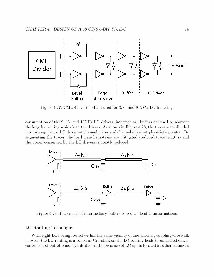
CHAPTER 4. DESIGN OF A 50 GS/S 6-BIT FI-ADC 74
Figure 4.27: CMOS inverter chain used for 3, 6, and 9 GHz LO buffering.
consumption of the 9, 15, and 18GHz LO drivers, intermediary buffers are used to segmentthe lengthy routing which load the drivers. As shown in Figure 4.28, the traces were dividedinto two segments: LO driver→ channel mixer and channel mixer→ phase interpolator. Bysegmenting the traces, the load transformations are mitigated (reduced trace lengths) andthe power consumed by the LO drivers is greatly reduced.
Figure 4.28: Placement of intermediary buffers to reduce load transformations.
LO Routing Technique
With eight LOs being routed within the same vicinity of one another, coupling/crosstalkbetween the LO routing is a concern. Crosstalk on the LO routing leads to undesired down-conversion of out-of-band signals due to the presence of LO spurs located at other channel’s

CHAPTER 4. DESIGN OF A 50 GS/S 6-BIT FI-ADC 75
LO frequencies. In order to reduce the amount of crosstalk, a planar twisted-pair routingtechnique is used to reject magnetic coupling between the the lines. The twisted-pair is avery common and useful RF technique used in communication systems (e.g. Ethernet) thateffectively reduces magnetic coupling by alternating the polarity of the induced emf on theconducting path [38]. Figure 4.29 illustrates how the planar twisted-pair was implementedusing the two top metal layers.
Figure 4.29: Planar twisted pair technique used for LO routing.
The planar twisted-pair rejects magnetic coupling onto the LO distribution lines. How-ever, the routing is still susceptible to electric coupling between nearby traces. The electriccoupling can also be viewed as capacitance that is accumulated bewtween two closely-spacedparallel metal wires and which provides a path for high-frequency signals to couple fromone wire to the other. This capacitance is formed when the two metal wires are at differ-ent potentials, causing the electric field lines of one wire to terminate on the other. If theinduced charge caused by electrical coupling does not have a low-resistive path to groundthen it will induce an undersired change in potential on the affected line; this is the natureof the electrical crosstalk. Shielding is the common solution to reducing electrical crosstalk[41]. As shown in Figure 4.29, planar ground shields are placed on both sides of the twistedpair. The ground shields are implemented on the top metal layer. Since the shield lines arenominally at zero potential, most of electric field lines eminating from the LO traces willterminate on the shield lines which provide a path to ground for any induced charge.
In order to retain a high common-mode rejection along the differential LO routes, theground shields are only shorted to ground at the source and load. This is because the groundshield is the return path for any common-mode signals, and thus, it is desirable to have a ahigh impedance on the common-mode return path in order to impedede any common-modecurrent flow. Of course, this is in contrast with the desired low-resistance needed on theground line for mitigating electric coupling, so a reasonable tradeoff must be made.

76
Chapter 5
Measurements
5.1 FI-ADC Analog Front-End
As mentioned in the Chapter 4, the first phase of this project focused on the design ofthe analog front-end. The AFE is responsible for the distrbution and channelization of thewideband input signal while sustaining sufficient linearity and noise (SNDR) performancefor the specified resolution. A design of the FI-ADC AFE was taped out in a TSMC 65nmGP+ process. The die photo of the microchip is shown in Figure 5.1. As seen in Figure 4.4,the design includes a 9-stage DA which feeds the nine processing channels. Each processingchannel contains a gm stage, I/Q passive mixer, and 2nd order current-mode lowpass filter.In order to facilitate measurements, 50Ω differential output buffers are used to interfaceeach channel with external equipment. The LO generation and distribution is comprised offrequency dividers, SSB mixers, LO buffers and line drivers. Harmonic rejection is performedfor Channel 2 (3rd and 5th) and Channel 3 (3rd). In order to calibrate HRR performance,9-bit current DACs are utilized in the phase interpolators and gm-stages.

CHAPTER 5. MEASUREMENTS 77
Figure 5.1: Die photo of FI-ADC AFE.
5.2 Measurement Setup
The focus of the initial measurements of the FI-ADC was to assess the linearity and noiseperformance. The measurement setup used for testing is shown in Figure 5.2. A chip-on-board (COB) assembly was used for wirebonding the baseband outputs of each channel to ahost board with SMA connectors. The host board is then connected to a custom high-speedADC board used for digitization of the analog outputs. The high-speed ADC board passesthe digital data of each channel to a Virtex-7 FPGA via FMC connectors. The FPGA isprogrammed to offload the data from the ADCs and pass it to the PC for backend processingand signal reconstruction.
The initial implementation of the custom high-speed board contains two 3GS/s, 8-bitADCs (PN: ADC08B3000)1. As such, the I and Q paths of a single channel could beprocessed simultaneously in the backend. The high-speed ADCs have integrated 4kB bufferswhich allow for the offloading of the data at a user-defined rate of 100MHz. On-boardlowpass filters (ωc = 900MHz) are included to provide sufficient out-of-band attenuation ofaliased signals. As discussed in Chapter 4, the fully integrated system would require an6GS/s ADC in conjunction with a 6th order Inverse-Chebyshev filter. Since 6GS/s ADCs
1Generously donated by Texas Instruments.

CHAPTER 5. MEASUREMENTS 78
are not commercially available, 3GS/s ADCs had to be used along with appropriately chosenfilters. This means that only 900MHz of the full 1.5GHz bandwidth of each I/Q channelcould be utilized in the current measurement setup.
Die probing is utilized for connecting the high-frequency inputs. The left-side probe con-tains the RF input, 1.2V (LO GEN and Analog Core) and 2.4V power rails, input referencecurrent, and scan chain signals. The right-side probe brings in the differential 36GHz and48GHz signals. Two Keysight 50GHz signal generators are used for generating the differentialsignals.
Figure 5.2: Measurement setup.
Due to limited equipment availability, the 36GHz and 48GHz signals could not be gen-erated simultaneously. The initial method for generating the phase-coherent 36GHz and48GHz signals is illustrated in Figure 5.3. This method utilizes multiplication of a single3GHz source up to the desired frequencies. Filters are used to filter out any undesired har-monics generated during the multiplication process. The signal is fed single-endedly to thechip while the other terminal is tied to the input bias voltage. The one issue with thismethod was the amount of signal loss incurred after the last stage of quaruplers. The mea-sured output power of the quadruplers was +18dBm while the amount of signal loss due tothe filters, bias-tees, cables, and the probe itself was 19.5dB resulting in a delivered powerof -1.5dBm, which was insufficient to achieve locking with a single-ended drive. As such, thetwo 50GHz signal generator approach had to be adopted.
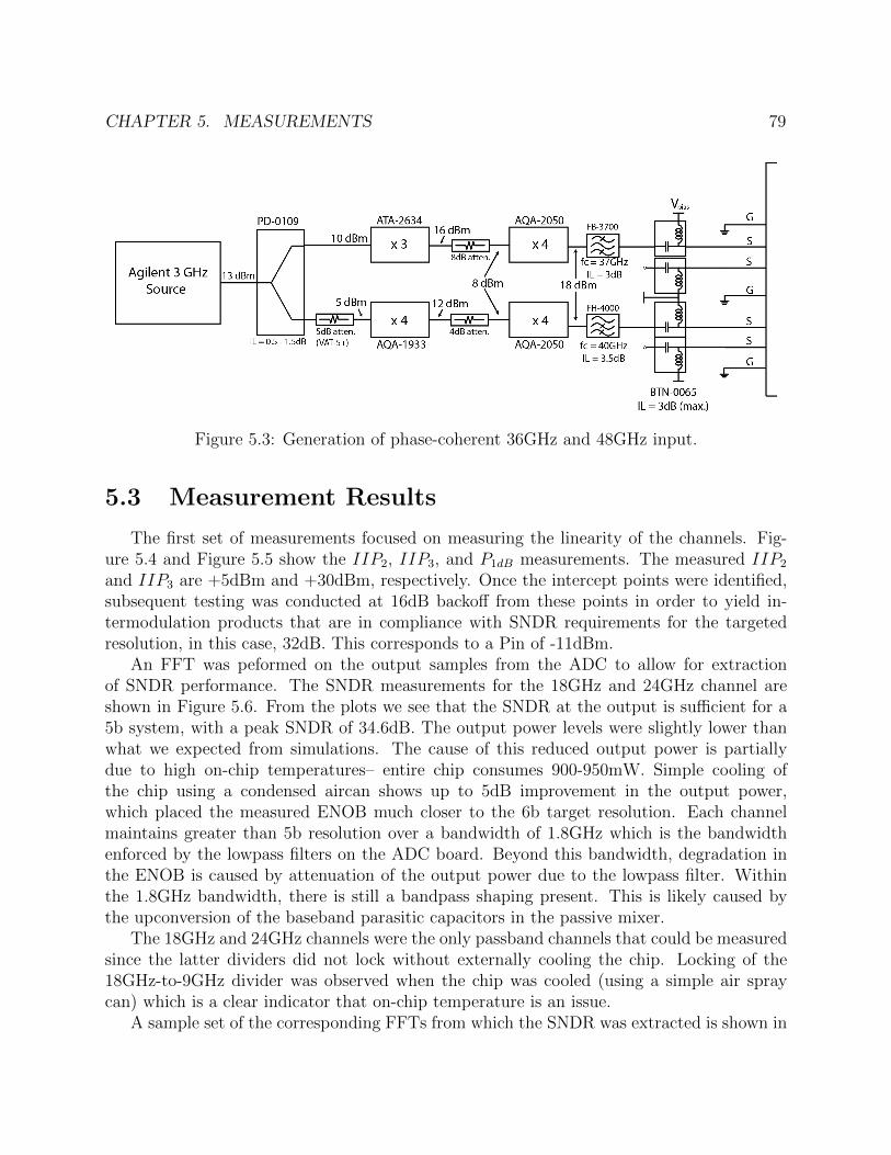
CHAPTER 5. MEASUREMENTS 79
Figure 5.3: Generation of phase-coherent 36GHz and 48GHz input.
5.3 Measurement Results
The first set of measurements focused on measuring the linearity of the channels. Fig-ure 5.4 and Figure 5.5 show the IIP2, IIP3, and P1dB measurements. The measured IIP2
and IIP3 are +5dBm and +30dBm, respectively. Once the intercept points were identified,subsequent testing was conducted at 16dB backoff from these points in order to yield in-termodulation products that are in compliance with SNDR requirements for the targetedresolution, in this case, 32dB. This corresponds to a Pin of -11dBm.
An FFT was peformed on the output samples from the ADC to allow for extractionof SNDR performance. The SNDR measurements for the 18GHz and 24GHz channel areshown in Figure 5.6. From the plots we see that the SNDR at the output is sufficient for a5b system, with a peak SNDR of 34.6dB. The output power levels were slightly lower thanwhat we expected from simulations. The cause of this reduced output power is partiallydue to high on-chip temperatures– entire chip consumes 900-950mW. Simple cooling ofthe chip using a condensed aircan shows up to 5dB improvement in the output power,which placed the measured ENOB much closer to the 6b target resolution. Each channelmaintains greater than 5b resolution over a bandwidth of 1.8GHz which is the bandwidthenforced by the lowpass filters on the ADC board. Beyond this bandwidth, degradation inthe ENOB is caused by attenuation of the output power due to the lowpass filter. Withinthe 1.8GHz bandwidth, there is still a bandpass shaping present. This is likely caused bythe upconversion of the baseband parasitic capacitors in the passive mixer.
The 18GHz and 24GHz channels were the only passband channels that could be measuredsince the latter dividers did not lock without externally cooling the chip. Locking of the18GHz-to-9GHz divider was observed when the chip was cooled (using a simple air spraycan) which is a clear indicator that on-chip temperature is an issue.
A sample set of the corresponding FFTs from which the SNDR was extracted is shown in
CHAPTER 5. MEASUREMENTS 80
Figure 5.7. The FFT plots exhibit spectral widening around the main signal. This wideningis not due to spectral spreading since the input frequencies were chosen to ensure coherentsampling with respect to the sampling frequency. Instead, this non-ideality was present inthe analog output spectrum as shown in Figure 5.8. It is suspected that these are noisesidebands caused by coupling between the input signal and the supply network resulting inundesired modulation. These noise sidebands are proportional to the input signal power leveland are also present in the baseband channel where no mixing is performed. The sidebandsare contained within a 20MHz bandwidth around the fundamental tone.
As demonstrated by Figure 5.9, these noise sidebands limit the measured ENOB. Thefigure shows a plot of the theoretical ENOB (ENOB ideal), raw ENOB (ENOB), and amodified ENOB (ENOB mod). The ENOB ideal response exhibits the 1 bit per 6dB slopeas predicted by theory. The raw ENOB is extracted from the unaltered FFT plots. Asseen in the figure, the raw ENOB only follows the theoretical trend for low input powers,after which it begins to degrade. This degradation is due to the increasing power levels ofthe noise sidebands which become higher than the thermal and quantization noise floor athigher input power levels. In order to get a measure of the ENOB due to the true noisefloor, and not the noise sidebands, the noise sidebands around the fundamental tone andits harmonics2 were set equal to the neighboring noise floor level. This modified ENOBmeasurement, ENOB mod, exhibits behavior much closer to what is expected when inputpower is increased. However, there is still degradation in ENOB mod at higher input powerlevels. The deviation above Pin = −15dBm is partly due to the onset of compression. Notethat ENOB mod is the reported ENOB for this design and what is reported in Figure 5.6.
Due to the locking issue with latter dividers, direct harmonic rejection measurementscould not be performed. In order to assess the potential harmonic rejection performance,indirect measurements of the phase interpolator were taken. Figure 5.10 shows the mea-sured phase response of the phase interpolator. Because of the non-ideal nature of themeasurement, the output signal was noisy and reliable phase measurements could only beperformed for 6 bits of resolution on the interpolator; the full resolution of the interpolatorwas 9 bits. With 6 bits of resolution, the worst-case phase step was measured to be 5.4
(Figure 5.11). Given this phase resolution, we performed a circuit-level simulation of themixer to assess the attainable harmonic rejection ratio subject to the worst-case resolution.From the simulation, the attainable HRR is 37dB.
The measured SNDR performance and indirectly measured HRR performance illustratethat the AFE is suitable to be used in a 5.5b ADC system. What’s left to be demonstratedis the reconstruction of a wideband signal (e.g. pulse-modulated carrier). Unfortunately, re-construction of a multi-channel signal was infeasible with the current measurement setup fortwo reasons. First, the custom high-speed ADC board only allowed simultaneous samplingof two outputs at a time, thus the best case would be sampling of I/Q of a single channel.Second, the frequency divider locking issue caused by on-chip heating prevents a majority
2These are harmonics of the baseband signal (post-downconversion) that are created by the final 50Ωoutput buffer

CHAPTER 5. MEASUREMENTS 81
of the channels from being measured consistently and reliably. Measurement setups thatprovide better heat removal from the die are being investigated.
Figure 5.4: IIP2/3 measurements.

CHAPTER 5. MEASUREMENTS 82
Figure 5.5: P1dB measurements.
Figure 5.6: SNDR measurements.
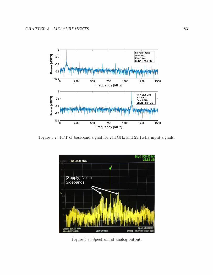
CHAPTER 5. MEASUREMENTS 83
Figure 5.7: FFT of baseband signal for 24.1GHz and 25.1GHz input signals.
Figure 5.8: Spectrum of analog output.

CHAPTER 5. MEASUREMENTS 84
Figure 5.9: Impact of noise sideband on measured ENOB.
Figure 5.10: Measured phase response of phase interpolator.
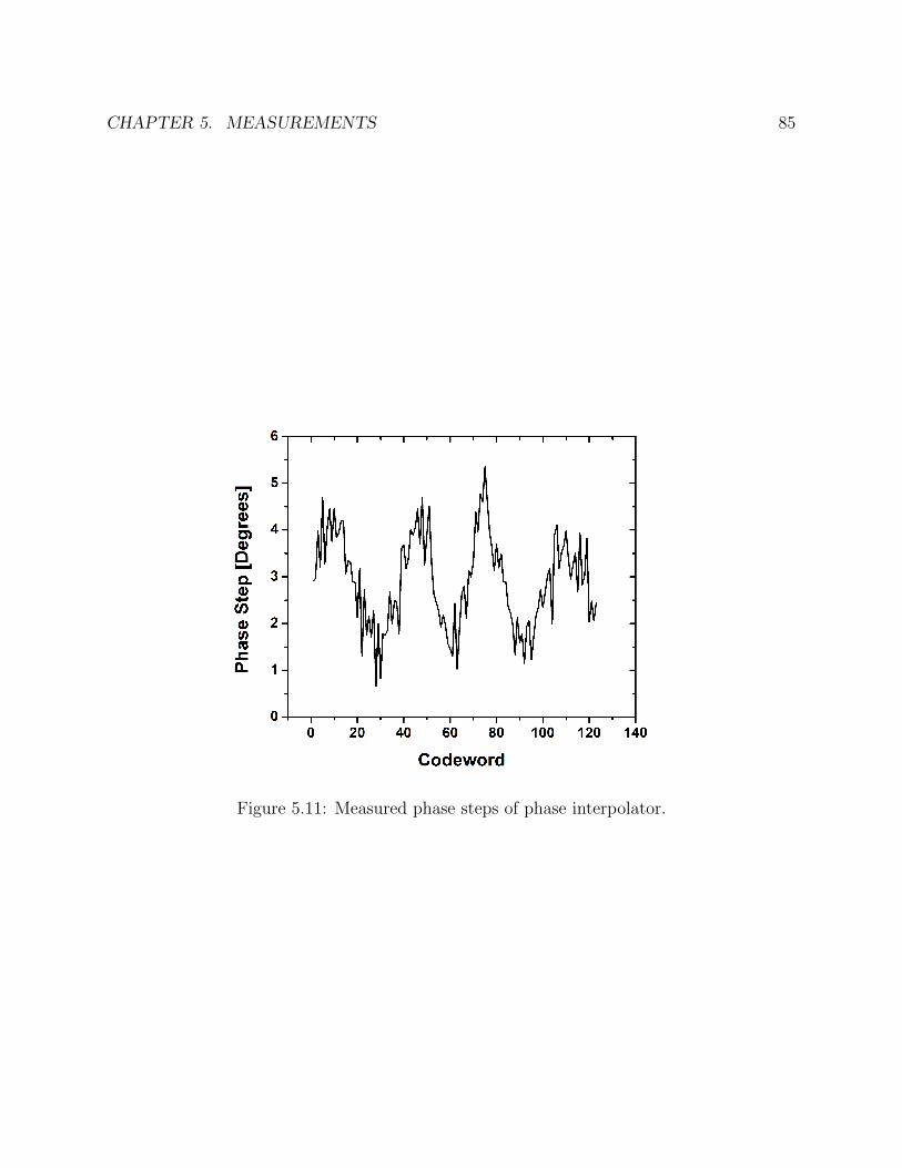
CHAPTER 5. MEASUREMENTS 85
Figure 5.11: Measured phase steps of phase interpolator.
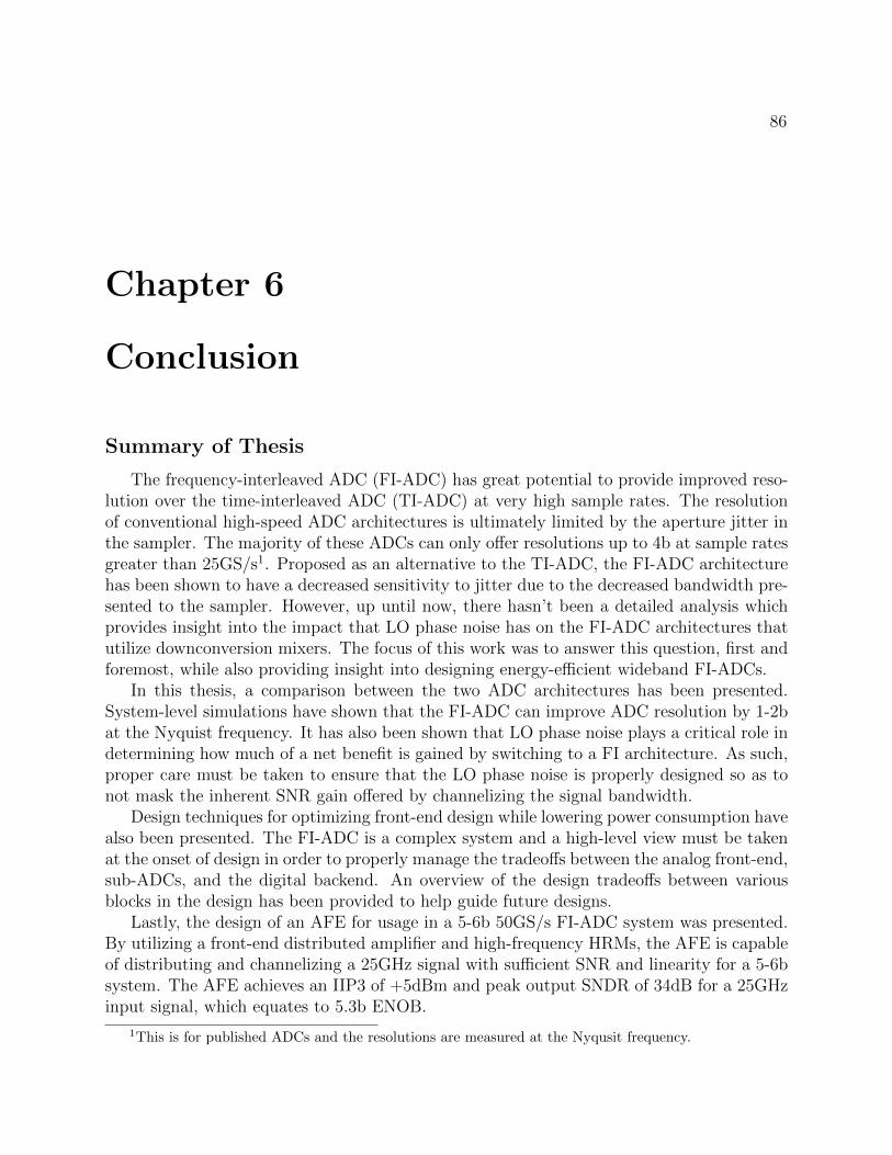
86
Chapter 6
Conclusion
Summary of Thesis
The frequency-interleaved ADC (FI-ADC) has great potential to provide improved reso-lution over the time-interleaved ADC (TI-ADC) at very high sample rates. The resolutionof conventional high-speed ADC architectures is ultimately limited by the aperture jitter inthe sampler. The majority of these ADCs can only offer resolutions up to 4b at sample ratesgreater than 25GS/s1. Proposed as an alternative to the TI-ADC, the FI-ADC architecturehas been shown to have a decreased sensitivity to jitter due to the decreased bandwidth pre-sented to the sampler. However, up until now, there hasn’t been a detailed analysis whichprovides insight into the impact that LO phase noise has on the FI-ADC architectures thatutilize downconversion mixers. The focus of this work was to answer this question, first andforemost, while also providing insight into designing energy-efficient wideband FI-ADCs.
In this thesis, a comparison between the two ADC architectures has been presented.System-level simulations have shown that the FI-ADC can improve ADC resolution by 1-2bat the Nyquist frequency. It has also been shown that LO phase noise plays a critical role indetermining how much of a net benefit is gained by switching to a FI architecture. As such,proper care must be taken to ensure that the LO phase noise is properly designed so as tonot mask the inherent SNR gain offered by channelizing the signal bandwidth.
Design techniques for optimizing front-end design while lowering power consumption havealso been presented. The FI-ADC is a complex system and a high-level view must be takenat the onset of design in order to properly manage the tradeoffs between the analog front-end,sub-ADCs, and the digital backend. An overview of the design tradeoffs between variousblocks in the design has been provided to help guide future designs.
Lastly, the design of an AFE for usage in a 5-6b 50GS/s FI-ADC system was presented.By utilizing a front-end distributed amplifier and high-frequency HRMs, the AFE is capableof distributing and channelizing a 25GHz signal with sufficient SNR and linearity for a 5-6bsystem. The AFE achieves an IIP3 of +5dBm and peak output SNDR of 34dB for a 25GHzinput signal, which equates to 5.3b ENOB.
1This is for published ADCs and the resolutions are measured at the Nyqusit frequency.

CHAPTER 6. CONCLUSION 87
Future Work and Directions
While this work has focused on some key fundamental questions regarding the FI-ADC,there are a lot more questions to be answered. For one, a measurement setup for comparingthe direct sampling architecture to the mix-then-sample setup would be informative anduseful for backing the presented theory. This measurement setup would parallel the simula-tion setup used in Chapter 3 and feature only the front-end sampling network of TI-ADCsand the AFE of the FI-ADC. To simplify the comparison, the two architectures could becompared only at the Nyqusit frequency since it yields the worst-case performance for botharchitectures. This will simplify the FI-ADC design since only a single channel needs to bedesigned.
Another key question to answer is whether or not the FI-ADC is a contender to theTI-ADC at lower sampling frequencies. Although the TI-ADC can provide 8-10b ENOBfor sampling frequencies of 1-5GS/s, there are still emerging applications that need to pushthe performance up to 12 bits – a very difficult task in the presence of the jitter barrier(Figure 1.1) – and the FI-ADC may pave the way to those additional two bits. Now, at veryhigh sampling frequencies (such as the targeted design for this work), a drawback of the FI-ADC is the intimidating overhead of generating and distributing the multiple LO frequencies.However, at lower frequencies, this may become less of an issue since distribution becomes(relatively) easier and the generation of multiple LOs can be done with advanced digitaltechniques as was done in [20]. Building on the techniques of [20], further work can be doneto push the attaianble ENOB of the FI architecture at sampling frequencies of 1-5GS/s.
Lastly, another concern for the FI-ADC, which wasn’t discussed in this thesis, is the powerconsumption of the digital backend. Methods for handling and processing multiple high-speed data channels in an energy-efficient manner are essential to keeping the FI-ADC figure-of-merit comparable to that of the TI-ADC. These methods will likely require innovationsat both the circuit and system level.
General Thoughts and Comments
Throughout this project, I have had countless discussions with professors and industrymembers about whether the FI-ADC is truly better than the TI-ADC. The response isgenerally mixed. On one hand, there are potential believers in the FI-ADC who recognizethe severity of the jitter problem and who believe that there is some potential to alleviate thisissue with the FI architecture. On the other hand, there are skeptics who immediately, andjustifiably, raise the question of phase noise introduced during the mixing process, claimingthat the jitter problem has simply been transferred to the mixer and therefore, there is noperformance benefit in moving to a FI architecture. My answer to this is always: it depends.As I have hopefully demonstrated in this thesis, the phase noise of the LO plays a criticalrole in determining the performance gain, if any, afforded by moving to an FI architecture.As seen from the simulation results, there are scenarios where the FI-ADC can outperformthe TI-ADC depending on how the LO is designed and distributed. My hope is that these

CHAPTER 6. CONCLUSION 88
results may help curb the skepticism and instead prompt a more detailed look into whetheror not the FI architecture is suitable for a particular application.
I would be remiss if I did not mention my own doubts and struggles with the FI architec-ture and its performance in comparison to the TI architecture. It is a very subtle problem.However, after countless hours mulling over the equations, the theory, and the simulations,my belief is that the FI-ADC is an answer to the jitter problem faced by current state-of-the-art high-speed ADCs, provided it is designed properly. I guess, in a sense, my answer isstill: it depends. The main question is whether the sacrificed ENOB at lower frequencies isjustified by the gains at the very high-frequencies (Figure 3.13). This is dependent on theapplication and a decision that needs to be made by the engineering architect. If filteringis utilized in the LO distribution (via tuned LO drivers), then the answer may be trivialsince the FI architecture may outperform the TI architecture across the board as it did inFigure 3.16. However, depending on the LO generation/distribution employed, the usageof tuned buffers may not be an option, especially considering the large area consumed byinductors, and the performance comparison may be closer to that of Figure 3.18. Still, asbandwidth demands increase and new applications emerge, the FI architecture may be uti-lized more frequently for the accurate digitization of very high frequencies,. This is alreadyhappening in the oscilloscope industry where an increasing number of high-end oscilloscopesuse the FI architecture (e.g. Teledyne LeCroy). Perhaps this trend will spread to the manyother high-speed applications.

89
Bibliography
[1] C. Wu and B. Nikolic, “A 0.4 GHz - 4 GHz direct RF-to-digital Σ∆ multi-mode re-ceiver,” in 2013 Proceedings of the ESSCIRC (ESSCIRC), Sept 2013, pp. 275–278.
[2] A. Arbabian, “Time-Domain Ultra-Wideband Synthetic Imager in Silicon,” Ph.D. dis-sertation, University of California, Berkeley, 2011.
[3] A. Arbabian, S. Callender, S. Kang, B. Afshar, J.-C. Chien, and A. M. Niknejad, “A90 GHz Hybrid Switching Pulsed-Transmitter for Medical Imaging,” IEEE Journal ofSolid-State Circuits, vol. 45, no. 12, pp. 2667 –2681, Dec. 2010.
[4] A. Arbabian, S. Callender, S. Kang, M. Rangwala, and A. M. Niknejad, “A 94 GHz mm-Wave-to-Baseband Pulsed-Radar Transceiver with Applications in Imaging and GestureRecognition,” IEEE Journal of Solid-State Circuits, vol. 48, no. 4, pp. 1055–1071, Apr.2013.
[5] S. Velazquez, “Hybrid Filter Banks for Analog/Digital Conversion,” Ph.D. dissertation,Massachusetts Institute of Technology, 1996.
[6] J. Black, W.C. and D. Hodges, “Time interleaved converter arrays,” IEEE Journal ofSolid-State Circuits, vol. 15, no. 6, pp. 1022–1029, Dec 1980.
[7] R. Walden, “Analog-to-Digital Converter Survey and Analysis,” IEEE Journal on Se-lected Areas in Communications, vol. 17, no. 4, pp. 539–550, Apr. 1999.
[8] B. Murmann, ADC Performance Survey 1997-2015. [Online]. Available: http://web.stanford.edu/∼murmann/adcsurvey.html
[9] E. Alon, EE240 Class Notes Spring 2009.
[10] L. Kull, T. Toifl, M. Schmatz, P. Francese, C. Menolfi, M. Braendli, M. Kossel, T. Morf,T. Andersen, and Y. Leblebici, “A 90GS/s 8b 667mW 64x Interleaved SAR ADC in32nm digital SOI CMOS,” in 2014 IEEE International Solid-State Circuits ConferenceDigest of Technical Papers (ISSCC), Feb 2014, pp. 378–379.

BIBLIOGRAPHY 90
[11] N. Kurosawa, H. Kobayashi, K. Maruyama, H. Sugawara, and K. Kobayashi, “Explicitanalysis of channel mismatch effects in time-interleaved ADC systems,” IEEE Transac-tions on Circuits and Systems I: Fundamental Theory and Applications, vol. 48, no. 3,pp. 261–271, Mar 2001.
[12] D. Stepanovic and B. Nikolic, “A 2.8 GS/s 44.6 mW Time-Interleaved ADC Achieving50.9 dB SNDR and 3 dB Effective Resolution Bandwidth of 1.5 GHz in 65 nm CMOS,”IEEE Journal of Solid-State Circuits, vol. 48, no. 4, pp. 971–982, April 2013.
[13] N. Le Dortz, J.-P. Blanc, T. Simon, S. Verhaeren, E. Rouat, P. Urard, S. Le Tual,D. Goguet, C. Lelandais-Perrault, and P. Benabes, “A 1.62GS/s time-interleaved SARADC with digital background mismatch calibration achieving interleaving spurs below70dBFS,” in 2014 IEEE International Solid-State Circuits Conference Digest of Tech-nical Papers (ISSCC), Feb 2014, pp. 386–388.
[14] X. Yi, C. Boon, H. Liu, J. Lin, J. Ong, and W. Lim, “A 57.9-to-68.3GHz 24.6mWfrequency synthesizer with in-phase injection-coupled QVCO in 65nm CMOS,” in2013 IEEE International Solid-State Circuits Conference Digest of Technical Papers(ISSCC), Feb 2013, pp. 354–355.
[15] V. Szortyka, Q. Shi, K. Raczkowski, B. Parvais, M. Kuijk, and P. Wambacq, “A 42mW230fs-jitter sub-sampling 60GHz PLL in 40nm CMOS,” in 2014 IEEE InternationalSolid-State Circuits Conference Digest of Technical Papers (ISSCC), Feb 2014, pp. 366–367.
[16] K. Lee and W. Namgoong, “A 0.25 um CMOS 3b 12.5 GS/s frequency channelizedreceiver for serial-links,” in 2005 IEEE International Solid-State Circuits ConferenceDigest of Technical Papers (ISSCC), Feb 2005, pp. 336–337.
[17] S. Jalali Mazlouman, S. Sheikhaei, and S. Mirabbasi, “A prototype implementationof a two-channel frequency-translating hybrid ADC,” in 50th Midwest Symposium onCircuits and Systems (MWSCAS), Aug 2007, pp. 144–147.
[18] Jalali Mazlouman, S. and Sheikhaei, S. and Mirabbasi, S., “4- and 6-GS/s 4-bitfrequency-translating hybrid ADCs in 90-nm CMOS,” Analog Integrated Circuitsand Signal Processing, vol. 68, no. 3, pp. 329–340, 2011. [Online]. Available:http://dx.doi.org/10.1007/s10470-011-9604-y
[19] S. Hoyos, S. Pentakota, Z. Yu, E. Ghany, X. Chen, R. Saad, S. Palermo, and J. Silva-Martinez, “Clock-Jitter-Tolerant Wideband Receivers: An Optimized MultichannelFilter-Bank Approach,” IEEE Transactions on Circuits and Systems I: Regular Papers,vol. 58, no. 2, pp. 253–263, Feb 2011.
[20] T. Forbes and R. Gharpurey, “A 2 GS/s Frequency-Folded ADC-Based BroadbandSampling Receiver,” IEEE Journal of Solid-State Circuits, vol. 49, no. 9, pp. 1971–1983, Sept 2014.

BIBLIOGRAPHY 91
[21] G. Ding, C. Dehollain, M. Declercq, and K. Azadet, “Frequency-Interleaving Techniquefor High-Speed A/D Conversion,” in Proceedings of the 2003 International Symposiumon Circuits and Systems (ISCAS ’03), May 2003, pp. I–857 – I–860.
[22] S. Jalali Mazlouman, S. Sheikhaei, and S. Mirabbasi, “Digital Compensation Techniquesfor Frequency-Translating Hybrid Analog-to-Digital Converters,” IEEE Transactions onInstrumentation and Measurement, vol. 60, no. 3, pp. 758–767, March 2011.
[23] P. J. Pupalaikis and D. C. Graef, “High Bandwidth Real-Time Oscilloscope,” U.S.Patent 7 058 548, Jun 6, 2006.
[24] S. Hoyos, B. Sadler, and G. Arce, “Ultra-Wideband Multicarrier Communication Re-ceiver Based on Analog to Digital Conversion in the Frequency Domain,” in 2005 IEEEWireless Communications and Networking Conference, Mar 2005, pp. 782–787.
[25] J. Weldon, R. Narayanaswami, J. Rudell, L. Lin, M. Otsuka, S. Dedieu, L. Tee, K.-C.Tsai, C.-W. Lee, and P. Gray, “A 1.75-GHz highly integrated narrow-band CMOS trans-mitter with harmonic-rejection mixers,” IEEE Journal of Solid-State Circuits, vol. 36,no. 12, pp. 2003–2015, Dec 2001.
[26] A. Rafi, A. Piovaccari, P. Vancorenland, and T. Tuttle, “A harmonic rejection mixerrobust to RF device mismatches,” in 2011 IEEE International Solid-State Circuits Con-ference Digest of Technical Papers (ISSCC), Feb 2011, pp. 66–68.
[27] H. Zhang, T. Gao, S. Tan, and O. Shana’A, “A harmonic-rejection mixer with improveddesign algorithm for broadband TV tuners,” in 2012 IEEE Radio Frequency IntegratedCircuits Symposium (RFIC), June 2012, pp. 163–166.
[28] J. Weldon, “High Performance CMOS Transmitters for Wireless Communication,”Ph.D. dissertation, University of California, Berkeley, 2005.
[29] C. Azeredo-Leme, “Clock Jitter Effects on Sampling: A Tutorial,” IEEE Circuits andSystems Magazine, vol. 11, no. 3, pp. 26–37, 2011.
[30] B. Lathi, Signal Processing and Linear Systems. Oxford University Press, 2000.
[31] W. Kester, Converting Oscillator Phase Noise to Time Jitter, Tutorial MT-008, Analog Devices, 2009. [Online]. Available: http://www.analog.com/media/en/training-seminars/tutorials/MT-008.pdf
[32] W. Egan, Frequency Synthesis by Phase Lock. Wiley-Interscience, 1999.
[33] J. Beyer, S. Prasad, R. Becker, J. Nordman, and G. Hohenwarter, “MESFET Dis-tributed Amplifier Design Guidelines,” IEEE Transactions on Microwave Theory andTechniques, vol. 32, no. 3, pp. 268–275, Mar. 1984.

BIBLIOGRAPHY 92
[34] S. Jalali Mazlouman and S. Mirabbasi, “A Frequency-Translating Hybrid Architec-ture for Wide-Band Analog-to-Digital Converters,” IEEE Transactions on Circuits andSystems-II, vol. 54, no. 7, pp. 576–580, 2007.
[35] C. Paul, “Bandwidth of Digital Waveforms,” IEEE Practical Papers, Articles, and Ap-plication Notes, pp. 58–64, 2009.
[36] L. Ye, J. Chen, L. Kong, E. Alon, and A. M. Niknejad, “Design Considerations for aDirect Digitally Modulated WLAN Transmitter with Integrated Phase Path and Dy-namic Impedance Modulation,” IEEE Journal of Solid-State Circuits, vol. 48, no. 12,pp. 3160–3177, Dec. 2013.
[37] D. Pozar, Microwave Engineering. Wiley, 2004.
[38] A. Niknejad, Electromagnetics for High-Speed Analog and Digital Communication Cir-cuits. Cambridge, 2007.
[39] A. Pirola, A. Liscidini, and R. Castello, “Current-Mode, WCDMA Channel Filter WithIn-Band Noise Shaping,” IEEE Journal of Solid-State Circuits, vol. 45, no. 9, pp. 1770–1780, Sep. 2010.
[40] C. Kromer, G. von Buren, G. Sialm, T. Morf, F. Ellinger, and H. Jackel, “A 40-GHzstatic frequency divider with quadrature outputs in 80-nm CMOS,” IEEE Microwaveand Wireless Components Letters, vol. 16, no. 10, pp. 564–566, Oct 2006.
[41] H. Ott, Noise Reduction Techniques in Electronic Systems. John Wiley & Sons Inc.,1976.