winter 18 examination subject name:analog communication
TRANSCRIPT

MAHARASHTRA STATE BOARD OF TECHNICAL EDUCATION (Autonomous)
(ISO/IEC - 27001 - 2013 Certified)
WINTER– 18 EXAMINATION Subject Name:Analog Communication Model Answer Subject Code:
1
Page 1/34
17440
Important Instructions to examiners:
1) The answers should be examined by key words and not as word-to-word as given in themodel answer scheme.
2) The model answer and the answer written by candidate may vary but the examiner may tryto assess the understanding level of the candidate.
3) The language errors such as grammatical, spelling errors should not be given moreImportance (Not applicable for subject English and Communication Skills.
4) While assessing figures, examiner may give credit for principal components indicated in thefigure. The figures drawn by candidate and model answer may vary. The examiner may give credit for anyequivalent figure drawn.
5) Credits may be given step wise for numerical problems. In some cases, the assumed constantvalues may vary and there may be some difference in the candidate’s answers and model answer.
6) In case of some questions credit may be given by judgement on part of examiner of relevant answer based on candidate’s understanding.
7) For programming language papers, credit may be given to any other program based on equivalent concept.
Q. No.
Sub Q. N.
Answers Marking Scheme
1 a) Attempt any SIX of the following: 12- Total Marks
i) Write down different frequencies for following(frequency ranges).
(1) Voice frequency (2) High frequency (3) IR frequency (4) Visible frequency(light)
2M
Ans: (Four Correct frequencies – ½ mark each)
Sr. No
Frequency
Range
1 Voice Frequency
300 Hz to 3kHz
2 High Frequency
3 MHz to 30 MHz
3 IR Frequency
30 THz to 430 THz
Four Correct frequencies – ½ mark each

MAHARASHTRA STATE BOARD OF TECHNICAL EDUCATION (Autonomous)
(ISO/IEC - 27001 - 2013 Certified)
WINTER– 18 EXAMINATION Subject Name:Analog Communication Model Answer Subject Code:
2
Page 2/34
17440
4 Visible Spectrum (light)
375 THz to 750 THz
ii) Define modulation index in FM. What is maximum value of deviation ratio. 2M
Ans:
Definition (1 Mark)& Maximum Value (1 Mark)
Modulation Index of FM: It is defined as the ratio of Frequency Deviation (δ) to the modulating signal frequency (fm).
(OR)
Maximum value of deviation ratio=5
Definition (1 Mark)& Maximum Value (1 Mark)
iii) Define pulse modulation. State its types. 2M
Ans: (Correct definition – 1 mark, Both Types any two sub classification – 1 mark)
Pulse Modulation: It is defined as the modulation technique in which the various parameters of carrier signal which is the train of periodic rectangular pulses changes in accordance with the instantaneous value of modulating signal.
Types of Pulse Modulation:
Analog Pulse modulation ( ½ M )
PAM
PWM
PPM
Digital Pulse Modulation ( ½ M )
PCM
DM
ADM
Correct definition – 1 mark, Both Types any two sub classification – 1 mark

MAHARASHTRA STATE BOARD OF TECHNICAL EDUCATION (Autonomous)
(ISO/IEC - 27001 - 2013 Certified)
WINTER– 18 EXAMINATION Subject Name:Analog Communication Model Answer Subject Code:
3
Page 3/34
17440
iv) What are the different types of FM detector?
2M
Ans: (Any four correct types – 2 marks)
The different types of FM Detectors are:
1. Simple Slope Detector
2. Balanced Slope Detector
3. Ratio Detector
4. Phase Discriminator
5. FM Detector using Phase Locked Loop (PLL)
Any four correct types – 2 marks
v) Write any two drawbacks of TRF radio receiver. 2M
Ans: (any two correct drawbacks – 1 mark each) Drawbacks of TRF Receiver: 1. Instability due to oscillatory nature of RF amplifier.
2. Variation in bandwidth over tuning range.
3. Insufficient selectivity at high frequencies
4. Poor adjacent channel rejection capability.
any two correct drawbacks – 1 mark each
vi) Draw general equivalent circuit of transmission line.
2M
Ans:
Fig. General Equivalent circuit of transmission line
Correct drawing=2M
vii) Write two reasons of fading. 2M

MAHARASHTRA STATE BOARD OF TECHNICAL EDUCATION (Autonomous)
(ISO/IEC - 27001 - 2013 Certified)
WINTER– 18 EXAMINATION Subject Name:Analog Communication Model Answer Subject Code:
4
Page 4/34
17440
Ans: (any two correct reasons – 1 mark each) Major reasons of Fading: 1. Interference between waves that have travelled by slightly different paths. 2. Multipath Propagation 3. Variation in atmospheric conditions along the path of waves.
4. As the fading is a frequency selective process, the signal very close to each other in the
frequency domain will fade to a different extent.
any two correct reasons – 1 mark each
viii) What is electromagnetic polarization. 2M
Ans: Correct definition (2 Marks) The polarization of a plane EM wave is simply the orientation of the electric field vector with respect to the surface (i.e. looking at the horizon)
Correct definition =2 Marks
b) Attempt any TWO of the following: 08- Total Marks
i) Draw block diagram of basic electronic communication system and state the function of each block.
4M
Ans: ( Block Diagram – 2M, Block Explanation- 2 M)
i) Input signal: - The information can be in the form of sound, picture or data coming from computer.
ii) Input transducer: - it converts original information into equivalent electrical signal.
iii) Transmitter: - it converts electric equivalent into suitable form. It increases the power level of signal so that it can cover long distance.
iv) Communication Channel: - it is the medium used for transmission of electromagnetic e.g. from one place to another..it can be wire or optical fibre or free space.
Block Diagram – 2M, Block Explanation- 2 M

MAHARASHTRA STATE BOARD OF TECHNICAL EDUCATION (Autonomous)
(ISO/IEC - 27001 - 2013 Certified)
WINTER– 18 EXAMINATION Subject Name:Analog Communication Model Answer Subject Code:
5
Page 5/34
17440
v) Noise: - It is unwanted signal which gets added in transmitting signal.
vi) Receiver: - the received signal is demodulated & converted back to suitable form. vii) Output transducer: - It converts electrical signal into original form.
ii) Draw Yagiuda antenna with its radiation pattern. 4M
Ans: (Construction – 2 marks, Radiation Pattern – 2 marks)
Construction of Yagi-Uda Antenna
Radiation Pattern of Yagi-Uda Antenna
Labeled diagram – 2 marks, Radiation Pattern – 2 marks
iii) For transmission line, the incident voltage Ei = 6V, and Er = 3V. Calculate:
(1) Reflection coefficient
(2) Standing wave ratio
4M
Ans: (1)Reflection coefficient (2 Marks) (2) Standing wave ratio(2 Marks) Each correct

MAHARASHTRA STATE BOARD OF TECHNICAL EDUCATION (Autonomous)
(ISO/IEC - 27001 - 2013 Certified)
WINTER– 18 EXAMINATION Subject Name:Analog Communication Model Answer Subject Code:
6
Page 6/34
17440
(1)Reflection coefficient
Reflection coefficient R=Er/Ei
=3/6
R=0.5
(2) Standing wave ratio
SWR=Ei+Er/Ei-Er
=6+3/6-3
SWR =3
calculation -2M
Q. No.
Sub Q. N. Answers Marking Scheme
2 Attempt any FOUR of the following: 16- Total Marks
a Draw the block diagram of AM super heterodyne radio receiver and state the function of each block.
4M
Ans: (block diagram – 2 marks, explanation – 2 marks)
AM super heterodyne receiver works on the principle of super heterodyning. In the super heterodyne receiver, the incoming signal voltage is combined with a signal generated in the receiver. The local oscillator voltage is normally converted into a signal of a low fixed frequency with the help of mixer. The signal at this intermediate frequency contains the same modulation as the original carrier and it is now amplified and detected to reproduce the original modulating signal
block diagram – 2 marks, explanation – 2 marks

MAHARASHTRA STATE BOARD OF TECHNICAL EDUCATION (Autonomous)
(ISO/IEC - 27001 - 2013 Certified)
WINTER– 18 EXAMINATION Subject Name:Analog Communication Model Answer Subject Code:
7
Page 7/34
17440
Functions of each block- Receiving antenna- AM receiver operates in the frequency range of 540 KHz to 1640 KHz.
RF stage- Selects wanted signal and rejects all other signals and thus reduces the effect of noise. Mixer- Receives signal from RF stage Fs and the local oscillator Fo, and are mixed to produce intermediate frequency signal IF which is given as:
IF=Fo-Fs
Ganged Tuning- To maintain a constant difference between the local oscillator and RF signal frequency, gang capacitors are used.
IF stage- The IF signal is amplified by the IF amplifier with enough gain.
Detector-Amplified signal is detected by the detector to get original modulating signal. The detector also provides control signals to control the gain of IF and RF stage called as AGC.
AGC- Automatic gain control controls the gain of RF and IF amplifiers to maintain a constant output level at the speaker even though the signal strength at the antenna varies.
b Draw the circuit diagram of PWM using IC555. State its operation. 4M

MAHARASHTRA STATE BOARD OF TECHNICAL EDUCATION (Autonomous)
(ISO/IEC - 27001 - 2013 Certified)
WINTER– 18 EXAMINATION Subject Name:Analog Communication Model Answer Subject Code:
8
Page 8/34
17440
Ans:
(diagram – 2 marks, explanation – 2 marks)
Operation: i. The timer IC555 is operated in monostable mode.
ii. The negative going carrier pulses are to the differentiator formed by R1 & C1. The differentiator produces sharp negative pulses which are applied to trigger input pin (2) of IC 555.
iii. These triggering decides the starting instants (leading edge) of the PWM pulses. The PWM pulses go high at the instants of arrival of these triggering pulses.
iv. The termination of the pulses is dependent upon, a) R2, C2 discharge time b) The modulating signal applied to control input pin (5) v. The modulating signal applied to pin no (5) will vary the control voltage to IC 555 in accordance to the modulating voltage.
vi. As this voltage increases, the capacitor C2 is allowed to charge through R2 upto a higher voltage & hence for a longer time (as R2 C2 time constant is fixed). The width of the corresponding output pulse will increase due to this action. As soon as VC2 is equal to the control voltage, the PWM pulse goes to zero.
vii. Thus PWM signal is generated at the output pin (3) of IC555 as monostablemultivibrator.
diagram – 2 marks, explanation – 2 marks
c Draw the AM signal representation in :
(i) Time Domain (ii) Frequency Domain
4M

MAHARASHTRA STATE BOARD OF TECHNICAL EDUCATION (Autonomous)
(ISO/IEC - 27001 - 2013 Certified)
WINTER– 18 EXAMINATION Subject Name:Analog Communication Model Answer Subject Code:
9
Page 9/34
17440
Ans: (i) AM in Time domain (2Marks)
(ii)AM in frequency domain (2 Marks)
Each labeled correct representation -2M
d Explain standing waves with load terminal open circuited and short circuited. 4M
Ans: Standing waves with load terminal open circuited (2 Marks)
Standing waves: The forward and reflected waves on the incorrectly terminated transmission line produce an interference pattern known as Standing waves.
The concept of Standing wave can be best understood by considering the two cases of impedance mismatch at load or the antenna end of the transmission line.
Short circuit:
Each correct explanation- 2M

MAHARASHTRA STATE BOARD OF TECHNICAL EDUCATION (Autonomous)
(ISO/IEC - 27001 - 2013 Certified)
WINTER– 18 EXAMINATION Subject Name:Analog Communication Model Answer Subject Code:
10
Page 10/34
17440
The waveform below the transmission line shows the voltage and current at each point on the line.
We can measure these voltages and current at each point with the help of multimeter.
As shown the voltage is zero while the current is maximum because short circuit means zero impedance.
All the power is reflected back towards the source.
The voltage and current variations distribute themselves according to the wavelength of the signal.
The pattern repeats for every one-half wavelength.
The voltage and current levels at the source will be dependent on the signal wavelength and actual line.
Standing waves with load terminal short circuited (2 Marks)
Open Circuit:
It means infinite impedance, so that voltage at the end of the line is maximum and the current is zero.
All the energy is reflected, thereby setting up this stationary pattern of voltage and current standing waves.

MAHARASHTRA STATE BOARD OF TECHNICAL EDUCATION (Autonomous)
(ISO/IEC - 27001 - 2013 Certified)
WINTER– 18 EXAMINATION Subject Name:Analog Communication Model Answer Subject Code:
11
Page 11/34
17440
Practically, transmission line won’t have a short or open.
Instead, the load impedance will not be equal to the transmission line (characteristic)impedence.
e Compare ground wave and space wave propagation on the basis of:
(i) Frequency range (ii) Method of propagation.
4M
Ans: (two correct points – 2 marks each)
Sr. No
Parameters
Ground Wave Propagation
Space Wave Propagation
1 Frequency Range
30 kHz to 3 MHz
Above 30 MHz
2 Method of wave propagation
Surface Wave Propagation which
waves vertically Polarized.
Line of Sight Propagation with
waves horizontally Polarized.
Each correct point of comparision-2M
f Explain half dipole antenna ( Resonant antenna ) with its radiation patteren. 4M
Ans: Half wave dipole antenna (1 mark)
Explanation: (2 marks) 1. It is a resonant antenna
2. It is exact half wavelength (λ /2) long & open circuited at one end.
3. The dipole antennas have lengths λ /2 , λ , 3 λ /2 etc. which are all multiple of λ /2.
Diagram-1M
Explanation-2M
Radiation pattern-1M

MAHARASHTRA STATE BOARD OF TECHNICAL EDUCATION (Autonomous)
(ISO/IEC - 27001 - 2013 Certified)
WINTER– 18 EXAMINATION Subject Name:Analog Communication Model Answer Subject Code:
12
Page 12/34
17440
Hence they are resonant.
4. In half wave dipole antennas the forward waves & reflected waves exist. Hence radiation pattern is bidirectional. The radiation pattern of half wave dipole antenna is –
The radiation pattern (1 mark)
Q. No.
Sub Q. N.
Answers Marking Scheme
3 Attempt any FOUR of the following: 16- Total Marks
a State and explain the types of noise in communication system. 4M
Ans:
External Noise: Atmospheric Noise Atmospheric noise or static is caused by lighting discharges in thunderstorms and other natural electrical disturbances occurring in the atmosphere. These electrical impulses are random in
State or List =1M
Explanation=3M(Any three types)

MAHARASHTRA STATE BOARD OF TECHNICAL EDUCATION (Autonomous)
(ISO/IEC - 27001 - 2013 Certified)
WINTER– 18 EXAMINATION Subject Name:Analog Communication Model Answer Subject Code:
13
Page 13/34
17440
nature. Hence the energy is spread over the complete frequency spectrum used for radio communication. Extraterrestrial Noise There are numerous types of extraterrestrial noise or space noises depending on their sources. However, these may be put into following two subgroups. 1. Solar noise
2. Cosmic noise Solar Noise This is the electrical noise emanating from the sun. Under quite conditions, there is a steady radiation of noise from the sun. This results because sun is a large body at a very high temperature and radiates electrical energy in the form of noise over a very wide frequency spectrum including the spectrum used for radio communication. Cosmic noise Distant stars are also suns and have high temperatures. These stars, therefore, radiate noise in the same way as sun. The noise received from these distant stars is thermal noise (or black body noise) and is distributing almost uniformly over the entire sky. We also receive noise from the center of our own galaxy from other distant galaxies. Man-Made Noise (Industrial Noise) Man-made noise or industrial- noise is meant the electrical noise produced by such sources as automobiles and aircraft ignition, electrical motors and switch gears, leakage from high voltage lines, fluorescent lights, and numerous other heavy electrical machines. Internal Noise: Thermal Noise Conductors contain a large number of 'free" electrons and "ions" strongly bound by molecular forces. The ions vibrate randomly about their normal positions, however, this vibration being a function of the temperature. Continuous collisions between the electrons and the vibrating ions take place. Thus there is a continuous transfer of energy between the ions and electrons. This is the source of resistance in a conductor. There is a random motion of the electrons which give rise to noise voltage called thermal noise. Shot Noise The most common type of noise is referred to as shot noise which is produced by the random arrival of 'electrons or holes at the output element of PN junction. Transit Time Noise Another kind of noise that occurs in transistors is called transit time noise. Transit time is the duration of time that it takes for a current carrier such as a hole or current to move from the input to the output. Flicker Noise

MAHARASHTRA STATE BOARD OF TECHNICAL EDUCATION (Autonomous)
(ISO/IEC - 27001 - 2013 Certified)
WINTER– 18 EXAMINATION Subject Name:Analog Communication Model Answer Subject Code:
14
Page 14/34
17440
Flicker noise or modulation noise is the one appearing in transistors operating at low audio frequencies. Transistor Thermal Noise Within the transistor, thermal noise is caused by the emitter, base and collector internal resistances. Partition Noise Partition noise occurs whenever current has to divide between two or more paths, and results from the random fluctuations in the division.
b Differentiate between AM and FM on the basis of:
(i) Definition (ii) Bandwidth (iii) Modulation Index (iv) Application
4M
Ans: Sr. No.
Parameter AM FM
1 Definition
Amplitude of the carrier
signal is varied in
accordance to the
instantaneous value of
the modulating signal
keeping frequency and
phase of carrier constant.
Frequency of the
carrier signal is
varied in accordance
to the instantaneous
value of the
modulating signal
keeping amplitude
and phase of carrier
constant
2 Bandwidth BW = 2 fm
Requires less
bandwidth
BW = 2 (δ + fm (max))
OR
BW= 2fm(max) X
No. of sidebands
Requires more
bandwidth
3 Modulation Index m =
=
mf=
4 Application
(any relevant
point to be
considered)
Radio and TV
broadcasting, Video
transmission in TV
receivers etc.
Radio and TV
broadcasting, Sound
transmission in TV
receivers etc.
Each corect point- 1 mark

MAHARASHTRA STATE BOARD OF TECHNICAL EDUCATION (Autonomous)
(ISO/IEC - 27001 - 2013 Certified)
WINTER– 18 EXAMINATION Subject Name:Analog Communication Model Answer Subject Code:
15
Page 15/34
17440
c Describe the term virtual height with the help of diagram showing ionized layer and the path of wave.
4M
Ans:
Fig: Virtual height of an ionized layer
Virtual height: -The incident wave returns back to the earth due to refraction. In this process it
bends down gradually and not sharply, but the incident and reflected rays follow exactly the same
paths as those if the signal have been reflected from a surface located at greater height.
It is the height above the earth’s surface from which a refracted wave appears to have been
reflected. It is also defined as the maximum height that the hypothetical reflected wave would
have reached.
Diagram = 2 M
Description =2M
d Draw the circuit diagram of practical diode detector and explain its working. 4M
Ans: Circuit diagram of practical diode detector:
Circuit diagram= 2M
Explanation =2M

MAHARASHTRA STATE BOARD OF TECHNICAL EDUCATION (Autonomous)
(ISO/IEC - 27001 - 2013 Certified)
WINTER– 18 EXAMINATION Subject Name:Analog Communication Model Answer Subject Code:
16
Page 16/34
17440
Explanation- The circuit operates in the following manner-
The diode has been reversed so that now the negative envelope is demodulated. Due to this
negative AGC voltage will be developed.R1 and R2 ensures that there is a series DC path
to ground for diode.
R1 and C1 is the low pass used to remove RF ripple that is present in the detector o/p.
C2 is coupling capacitor that prevents the diode DC o/p from reaching the volume control
R4. Hence across R4 demodulated output is with zero dc shift which is applied to the AF
amplifier.
R3 and C3 is a low pass filter which removes AF components and helps to produce AGC
voltage.
The DC AGC voltage is proportional to the amplitude of AM signal.
e In a broadcast superheterodyne receiver having loaded Q of antenna coupling of 100, if intermediate frequency of 455 KHz, calculate image frequency and its rejection ratio at 1000 KHz.
4M
Ans:
Given:-Q=100
Intermediate frequency = IF= 455 KHz
Incoming signal Frequency Fs=1000 KHz
Calculate:- 1) fsi –Image frequency
2) Image frequency Rejection ratio
1) fsi is given as-
fsi= Fs+ 2 IF = 1000 x 103+ 2 (455 x 103)
fsi = 1910 KHz
Each correct calculation 2M

MAHARASHTRA STATE BOARD OF TECHNICAL EDUCATION (Autonomous)
(ISO/IEC - 27001 - 2013 Certified)
WINTER– 18 EXAMINATION Subject Name:Analog Communication Model Answer Subject Code:
17
Page 17/34
17440
2) Rejection ratio is given by
α =
Where Q is the loaded Q of tuned circuit or antenna coupling
ρ =
-
=
-
= 1.386
Q = 100
Therefore, α = = 138.60
f Explain power relations in AM wave. 4M
Ans:
Total power formula =1M
Carrier power=1M
Sideband power=1M
Relation between total and carrier power=1M

MAHARASHTRA STATE BOARD OF TECHNICAL EDUCATION (Autonomous)
(ISO/IEC - 27001 - 2013 Certified)
WINTER– 18 EXAMINATION Subject Name:Analog Communication Model Answer Subject Code:
18
Page 18/34
17440
Q. No.
Sub Q. N.
Answers Marking Scheme
4 Attempt any FOUR of the following: 16- Total Marks
a Define pre-emphasis. State its need. Draw the circuit of pre-emphasis. 4M
MAHARASHTRA STATE BOARD OF TECHNICAL EDUCATION (Autonomous)
(ISO/IEC - 27001 - 2013 Certified)
WINTER– 18 EXAMINATION Subject Name:Analog Communication Model Answer Subject Code:
19
Page 19/34
17440
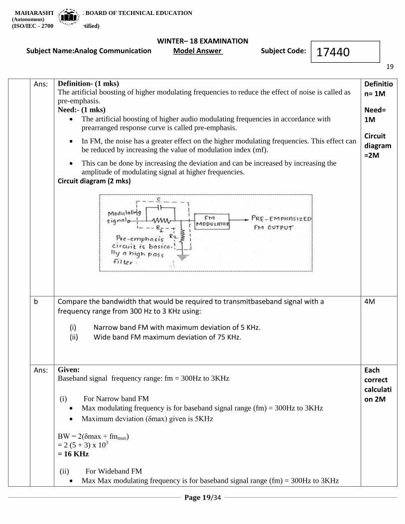
Ans: Definition- (1 mks) The artificial boosting of higher modulating frequencies to reduce the effect of noise is called as
pre-emphasis.
Need:- (1 mks)
The artificial boosting of higher audio modulating frequencies in accordance with
prearranged response curve is called pre-emphasis.
In FM, the noise has a greater effect on the higher modulating frequencies. This effect can
be reduced by increasing the value of modulation index (mf).
This can be done by increasing the deviation and can be increased by increasing the
amplitude of modulating signal at higher frequencies.
Circuit diagram (2 mks)
Definition= 1M
Need= 1M
Circuit diagram=2M
b Compare the bandwidth that would be required to transmitbaseband signal with a frequency range from 300 Hz to 3 KHz using:
(i) Narrow band FM with maximum deviation of 5 KHz. (ii) Wide band FM maximum deviation of 75 KHz.
4M
Ans: Given:
Baseband signal frequency range: fm = 300Hz to 3KHz
(i) For Narrow band FM
Max modulating frequency is for baseband signal range (fm) = 300Hz to 3KHz
Maximum deviation (δmax) given is 5KHz
BW = 2(δmax + fmmax)
= 2 (5 + 3) x 103
= 16 KHz
(ii) For Wideband FM
Max Max modulating frequency is for baseband signal range (fm) = 300Hz to 3KHz
Each correct calculation 2M

MAHARASHTRA STATE BOARD OF TECHNICAL EDUCATION (Autonomous)
(ISO/IEC - 27001 - 2013 Certified)
WINTER– 18 EXAMINATION Subject Name:Analog Communication Model Answer Subject Code:
20
Page 20/34
17440
Frequency deviation (δmax) given is = 75KHz
BW = 2(δmax + fmmax)
= 2 (75 + 3) x 103
= 2 x 78 x103
= 156 KHz
c Draw the structure and radiation pattern of parabolic dish antenna.
4M
Ans:
Dish antenna uses simple reflection principle, just as a mirror can reflect light and a curved mirror
can reflect and focus light at a single point, the dish reflects and focuses the radio waves.
This is the same principle and shape that is used as reflector in a flashlight or headlight behind the
bulb.
Dish antennas are used for systems that transmit and receive as well as receive only.
Structure = 2M
Radiation pattern= 2M
d For a transmission line , if R is the reflection co-efficient ,what will be its value.
(i) If there is no reflected voltage? (ii) If reflected and incident voltages are same? (iii) If reflected voltage = 10 V and incident voltage = 20V? (iv) If reflected voltage = 2V and incident voltage =2V?
4M
Ans: Reflection Coefficient R =
Each
correct calculati

MAHARASHTRA STATE BOARD OF TECHNICAL EDUCATION (Autonomous)
(ISO/IEC - 27001 - 2013 Certified)
WINTER– 18 EXAMINATION Subject Name:Analog Communication Model Answer Subject Code:
21
Page 21/34
17440
(i) If there is no reflected voltage That is Er = 0
Then R =
= 0
R = 0
(ii) If reflected and incident voltages are same That is Er = Ei
Then R =
= 1
R = 1
(iii) If reflected voltage = 10 V and incident voltage = 20V? That is Er = 10 and Ei = 20
Then R =
=
= 0.5
R= 0.5
(iv) If reflected voltage = 2V and incident voltage =2V?
Then R =
=
= 1
R= 1
on 1M
e Draw block diagram of tuned radio receiver with waveforms. 4M
Ans: Block Diagram of Tuned radio frequency receiver:
Diagram=2M
Waveforms at each block=2M

MAHARASHTRA STATE BOARD OF TECHNICAL EDUCATION (Autonomous)
(ISO/IEC - 27001 - 2013 Certified)
WINTER– 18 EXAMINATION Subject Name:Analog Communication Model Answer Subject Code:
22
Page 22/34
17440
f Explain :
(i) Critical frequency (ii) Skip distance
4M
Ans: Ans: (Each explanation - 2 marks)
i) Critical frequency: The critical frequency of a layer is defined as the maximum frequency that
is returned back to the earth by that layer, when the wave is incident at an angle 900(normal) to it.
ii) Skip distance: The skip distance is defined as the shortest distance from a transmitter,
measured along the surface of earth at which a sky wave of fixed frequency returns back to the
earth.
The frequency should be greater than critical frequency fc .
Each explanation =2M
Q. No.
Sub Q. N.
Answers Marking Scheme
5 Attempt any FOUR of the following: 16- Total Marks

MAHARASHTRA STATE BOARD OF TECHNICAL EDUCATION (Autonomous)
(ISO/IEC - 27001 - 2013 Certified)
WINTER– 18 EXAMINATION Subject Name:Analog Communication Model Answer Subject Code:
23
Page 23/34
17440
a Describe the FM generation using IC 566. 4M
Ans:
Explanation:
A common type of VCO available in IC form is NE/SE566. Referring to figure a timing
capacitor Ct is linearly charged or discharged by a constant current source/sink.
The amount of current can be controlled by charging the voltage Vc applying at the modulating input (pin 5) or by changing the timing resistor Rt external to IC chip.
The voltage at pin 6 is held at the same voltage as pin5. Thus if the modulating voltage at pin 5 is increased the voltage at pin 6 also increases, resulting in less voltage across Rt and thereby decreasing the charging current.
The output frequency of the VCO can be changed either by (i) Rt, (ii) Ct or (iii) The voltage Vc at the modulating input terminal pin 5. The voltage Vc can be varied by connecting a R1R2 circuit is shown in figure.
The component Rt and Ct are first selected so that VCO output frequency lies in the centre of the operating frequency range.
Now the modulating input voltage is usually varied from 0.75 Vcc to Vcc which can produce a frequency variation of about 10 to 1.
diagram – 2 marks, explanation – 2 marks
b State the need of AGC. Explain its types. 4M
Ans: Need Of AGC:2Marks ,Types:1 Marks,explaination:1marks
Need of AGC:-
The need or purpose of AGC circuit is to maintain the output voltage level (volume)
Need Of AGC:2M
Types:1 Marks,
MAHARASHTRA STATE BOARD OF TECHNICAL EDUCATION (Autonomous)
(ISO/IEC - 27001 - 2013 Certified)
WINTER– 18 EXAMINATION Subject Name:Analog Communication Model Answer Subject Code:
24
Page 24/34
17440
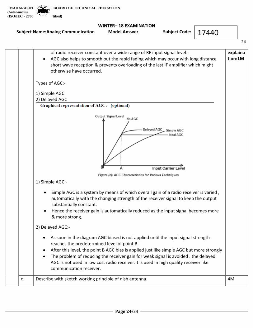
of radio receiver constant over a wide range of RF input signal level.
AGC also helps to smooth out the rapid fading which may occur with long distance short wave reception & prevents overloading of the last IF amplifier which might otherwise have occurred.
Types of AGC:-
1) Simple AGC 2) Delayed AGC
1) Simple AGC:-
Simple AGC is a system by means of which overall gain of a radio receiver is varied , automatically with the changing strength of the receiver signal to keep the output substantially constant.
Hence the receiver gain is automatically reduced as the input signal becomes more & more strong.
2) Delayed AGC:-
As soon in the diagram AGC biased is not applied until the input signal strength reaches the predetermined level of point B
After this level, the point B AGC bias is applied just like simple AGC but more strongly
The problem of reducing the receiver gain for weak signal is avoided . the delayed AGC is not used in low cost radio receiver.It is used in high quality receiver like communication receiver.
explaination:1M
c Describe with sketch working principle of dish antenna. 4M
MAHARASHTRA STATE BOARD OF TECHNICAL EDUCATION (Autonomous)
(ISO/IEC - 27001 - 2013 Certified)
WINTER– 18 EXAMINATION Subject Name:Analog Communication Model Answer Subject Code:
25
Page 25/34
17440
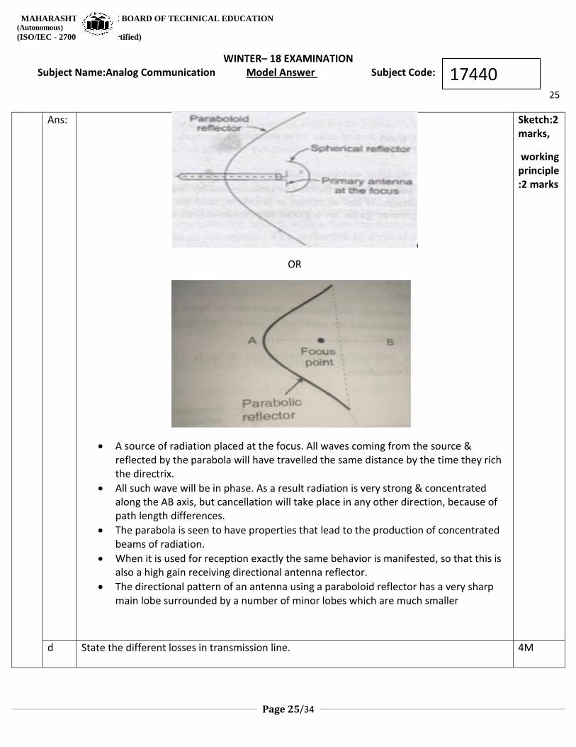
Ans:
OR
A source of radiation placed at the focus. All waves coming from the source & reflected by the parabola will have travelled the same distance by the time they rich the directrix.
All such wave will be in phase. As a result radiation is very strong & concentrated along the AB axis, but cancellation will take place in any other direction, because of path length differences.
The parabola is seen to have properties that lead to the production of concentrated beams of radiation.
When it is used for reception exactly the same behavior is manifested, so that this is also a high gain receiving directional antenna reflector.
The directional pattern of an antenna using a paraboloid reflector has a very sharp main lobe surrounded by a number of minor lobes which are much smaller
Sketch:2marks,
working principle:2 marks
d State the different losses in transmission line. 4M

MAHARASHTRA STATE BOARD OF TECHNICAL EDUCATION (Autonomous)
(ISO/IEC - 27001 - 2013 Certified)
WINTER– 18 EXAMINATION Subject Name:Analog Communication Model Answer Subject Code:
26
Page 26/34
17440
Ans: Losses in Transmission Line:-
There are three ways in which energy, applied to a transmission may desperate before reaching the load. They are
1) Radiation Losses:-
Its occurs when a transmission line may act as an antenna when the separation of the conductor is an appreciable fraction of a wave length .
This loss increase with frequency for any given transmission line eventually ending that lines usefulness at some high frequency.
This loss is more in parallel wire lines than to coaxial lines.
2) Conductor Or I2 R loss:-
This loss is proportional to the current and their fore inversely proportional to characteristics impedance
It also increases with frequency, this time because of the skin effect.
3) Dielectric loss:
This loss is proportional to the voltage across the dielectric and hence inversely proportional to the characteristic impedance for any power transmitted.
It again increases with frequency because a gradually worsening properties with increasing frequency for any given dielectric medium.
4) Corona Effect:-
Corona is a luminance discharge that occurs between the two conductors of a transmission line when the difference of proportional between them exceeds the break down voltage of the dielectric insulator.
Generally when corona occurs, the transmission line is destroyed.
1 marks for each loss explanation
e Describe the application of transmission line as stub. Write the situation where single stub or double stub is used.
4M
Ans:
Stub:2 marks,single stub:1 marks,double stub:1 marks
Stub:-Stub is the piece of short circuited transmission line which is used to tune out the reactance of the load when connected the transmission line as close as possible
Single stub: Stub is the piece of short circuited TL which is used to tune out the reactance of the load
Stub:2 marks,
single stub:1

MAHARASHTRA STATE BOARD OF TECHNICAL EDUCATION (Autonomous)
(ISO/IEC - 27001 - 2013 Certified)
WINTER– 18 EXAMINATION Subject Name:Analog Communication Model Answer Subject Code:
27
Page 27/34
17440
when connected across the TL as close as possible.
1. The most important feature of single stub matching is that the stub should be located as near to the load as possible.
2. The characteristic admittance of the stub so connected in shunt should be same as that of the main line.
3. The main element of this transmission line is a short circuited section of line whose open end is connected to the main line at a particular distance from the load end.
4. Where the input conductance at that point is equal to the characteristic conductance of the line, and the stub length is adjusted to provide a susceptance equal in value but opposite in sign, to the input susceptance of the main line at that point.
5. So the total susceptance of the main line at that point is zero.
6. The combination of stub and the line will thus present a conductance which is equal to the characteristic impedance of the line, i.e. the main length of the HF transmission line will be matched.
Double stub:
(i) The disadvantages of single stub matching are overcome by using double stub matching as shown in fig.
marks,
double stub:1 marks

MAHARASHTRA STATE BOARD OF TECHNICAL EDUCATION (Autonomous)
(ISO/IEC - 27001 - 2013 Certified)
WINTER– 18 EXAMINATION Subject Name:Analog Communication Model Answer Subject Code:
28
Page 28/34
17440
Here, two short circuited stubs at two fixed point usually 4 apart are utilized.
(ii) Their positions are fixed but lengths are independently adjustable.
(iii) The double stub matching provides wide range of impedance matching.
f What is frequency changing and tracking? 4M
Ans:
Mixer is the frequency changer which is a nonlinear circuit, having two sets of i/p terminals and one set of o/p terminals. The signal from antenna or RF stage Fs is fed to one of the i/p and the other i/p is from the local oscillator Fo. The mixer produces several frequencies at the o/p, among which Fo – Fs is called as the intermediate frequency Fi. (1 marks)
Frequency Tracking:-The super heterodyne receiver has to a no of tunable circuits which must be tuned correctly if any given station is to be received. So any error should not occur, called as tracking errors Thus frequency tracking is the process in which the local oscillator frequency follows or tracks
Frequency changing:2 marks,
tracking:2 marks

MAHARASHTRA STATE BOARD OF TECHNICAL EDUCATION (Autonomous)
(ISO/IEC - 27001 - 2013 Certified)
WINTER– 18 EXAMINATION Subject Name:Analog Communication Model Answer Subject Code:
29
Page 29/34
17440
the signal frequency to have a correct frequency difference for IF stage.
There are two types of tracking
a) two point tracking
b) three point tracking
Q. No.
Sub Q. N.
Answers Marking Scheme
6 Attempt any TWO of the following: 16- Total Marks
a What are different microwave antenna? Explain horn antenna with neat sketch. Explain loop antenna.
8M
Ans: List antennas:2marks,horn antenna sketch:2marks,explaination:2marks,loop antenna diagram:1 marks, explanation :1 marks
Types of microwave antennas: i) Dish antenna ii) Horn antenna
Horn antenna:
1. It is basically a waveguide terminated by horn.
2. Waveguide is a hollow metallic pipe used to carry electromagnetic waves at microwave frequencies.
3. All the energy travelling forward in the waveguide is radiated very effectively with the addition of the horn.
4. There are three configuration s of most commonly used Horn antennas, i) Sectorial ii) Pyramidal iii) Conical
List antennas:2marks,
horn antenna sketch:2marks,
explaination:2marks,
loop antenna diagram:1 marks,
explana

MAHARASHTRA STATE BOARD OF TECHNICAL EDUCATION (Autonomous)
(ISO/IEC - 27001 - 2013 Certified)
WINTER– 18 EXAMINATION Subject Name:Analog Communication Model Answer Subject Code:
30
Page 30/34
17440
As shown in fig
. i) The Sectorial horn flares out only in one direction.
ii) Pyramidal horn flares out in both directions and has the shape of truncated pyramid
Iii) The Conical horn is the termination of a circular waveguide.
The ratio of L/decides the beam width and the gain of the antenna
There are two types of Horn antenna a) Cass- horn antenna
b) Hog Horn antenna
Loop antenna
Loop antenna-The single turn coil carrying RF current through it having length less than the wavelength. (1 mark)
tion :1 marks

MAHARASHTRA STATE BOARD OF TECHNICAL EDUCATION (Autonomous)
(ISO/IEC - 27001 - 2013 Certified)
WINTER– 18 EXAMINATION Subject Name:Analog Communication Model Answer Subject Code:
31
Page 31/34
17440
b Derive the equation for characteristic impedance of transmission line at low frequency and high frequency. State four characteristics of transmission line.
8M
Ans: Equation for characteristic impdance of transmission line at low ferquency:2 marks,high frquency:2 marks,any 4 chracteristics of transmission lie:4 marks
Characteristics of transmission line:
1. Parameters
2. Characteristics impedance is resistive at radio frequencies.
Each correct equation-2Mx2=4M
Four characteristics-4M

MAHARASHTRA STATE BOARD OF TECHNICAL EDUCATION (Autonomous)
(ISO/IEC - 27001 - 2013 Certified)
WINTER– 18 EXAMINATION Subject Name:Analog Communication Model Answer Subject Code:
32
Page 32/34
17440
3. SWR=
4. Transformer and impedance matching.
5. Open and short circuited lines as tuned circuit.
6. Lines of various lengths are equivalent L and C parallel or series.
c Explain Duct propagation. Explain ionosphere layer and the ionospheric propagation. 8M
Ans: Duct propagation diagram:2 marks,explination:2marks,Ionosphere layer explaination:2 marks, propagation:2marks
Duct propagation is a special type and used for very high microwave frequencies.
New phenomenon which occurs in super-refraction, also known as ducting.
As the height above earth increases, the air density decreases and refractive index increases.
Under certain special atmospheric conditions, a layer of warm air may be trapped above cooler air, often over the surface of water.
So that refractive index will decrease far more rapidly with height than is usual.
This happens near ground within 30 m of it.
Due to this rapid reduction of refractive index, the microwaves completely bend back towards earth surface as shown in fig.
Microwaves are thus continuously refracted in duct and reflected back by the ground, so that they are propagated around the curvature of the earth for distances which many of times exceed 1000km.
The main requirement of formation of atmospheric ducts is the so-called temperature inversion.
Temperature inversion is the increase of air temperature with height, instead of the usual
Duct propagation diagram:2 M
explination:2M
Ionosphere layer explaination:2M
propagation:2M

MAHARASHTRA STATE BOARD OF TECHNICAL EDUCATION (Autonomous)
(ISO/IEC - 27001 - 2013 Certified)
WINTER– 18 EXAMINATION Subject Name:Analog Communication Model Answer Subject Code:
33
Page 33/34
17440
decrease in temperature of 6.50C/km in the standard atmosphere.
The Duct propagation is used for very high frequencies in GHz range.
The Ionosphere is the upper portion of the atmosphere. The ultra violet radiation from the sun will ionize the upper layer of the atmosphere. Due to ionization these part of the atmosphere becomes electrically charged. In this layer free electrons and positive and negative ions are present and hence this layer of ions is known as ionosphere.
There are four layers: D, E, F1 and F2.
1. D Layer: It is lowest layer at an height of 70 kms with thickness 10 km. The ionization density is maximum at noon and disappears at night.
2. E Layer: It is the next layer at an height of 100 kms with thickness 25 km. The layer disappears at night due to recombination of ions and molecules.
3. F1Layer: It is the next layer at an height of 180 kms with thickness 20 km. It provides more absorption for HF waves.
4. F2Layer: It is the next layer at an height of 250-400 kms with thickness 200 km. It is having highest electron density of all layers, due to this F2 layer remains present at night time.

MAHARASHTRA STATE BOARD OF TECHNICAL EDUCATION (Autonomous)
(ISO/IEC - 27001 - 2013 Certified)
WINTER– 18 EXAMINATION Subject Name:Analog Communication Model Answer Subject Code:
34
Page 34/34
17440
Ionosphere Propagation:
In this propagation, the transmitted signal transmits into the upper atmosphere where it is bent i.e reflected back to earth. This bending of the signal takes place due to the presence of the ionosphere layer.
Its Frequency Range is from 3 MHz to 30 MHz
Polarization: Vertical