wjec eduqas gce a level in electronics
TRANSCRIPT
WJEC Eduqas GCE A LEVEL in
ELECTRONICS
Teaching from 2017For award from 2019
SPECIFICATION
GCE A LEVEL
ACCREDITED BY OFQUALDESIGNATED BY QUALIFICATIONS WALES

A LEVEL ELECTRONICS 1
© WJEC CBAC Ltd.
WJEC Eduqas GCE A LEVEL ELECTRONICS
For teaching from 2017 For award from 2019
Page
Summary of assessment 2
1. Introduction 3 1.1 Aims and objectives 3 1.2 Prior learning and progression 4 1.3 Equality and fair access 4
2. Subject content 5 2.1 Component 1 13 2.2 Component 2 26 2.3 Component 3 37
3. Assessment 41 3.1 Assessment objectives and weightings 41 3.2 Arrangements for non-exam assessment 42
4. Technical information 43 4.1 Making entries 43 4.2 Grading, awarding and reporting 43
Appendices: 44 A: Equations in electronics 44 B: Mathematical requirements and exemplification 48 C: Electronic symbols 50 D: Independence in non-exam assessment tasks 52 E: Assessment grids for non-exam assessment 57
A LEVEL ELECTRONICS 2
© WJEC CBAC Ltd.
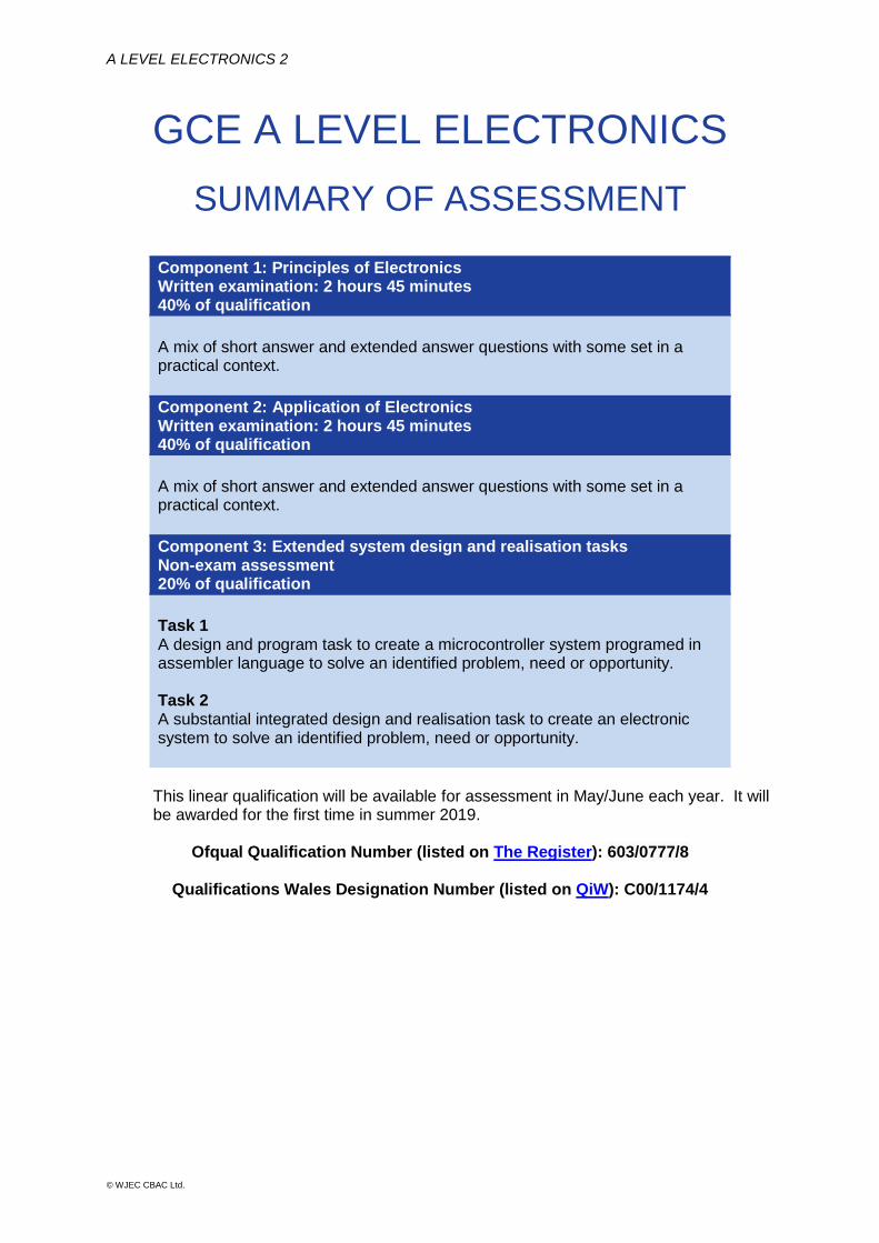
GCE A LEVEL ELECTRONICS
SUMMARY OF ASSESSMENT
Component 1: Principles of Electronics Written examination: 2 hours 45 minutes 40% of qualification
A mix of short answer and extended answer questions with some set in a practical context.
Component 2: Application of Electronics Written examination: 2 hours 45 minutes 40% of qualification
A mix of short answer and extended answer questions with some set in a practical context.
Component 3: Extended system design and realisation tasks Non-exam assessment 20% of qualification
Task 1 A design and program task to create a microcontroller system programed in assembler language to solve an identified problem, need or opportunity. Task 2 A substantial integrated design and realisation task to create an electronic system to solve an identified problem, need or opportunity.
This linear qualification will be available for assessment in May/June each year. It will be awarded for the first time in summer 2019.
Ofqual Qualification Number (listed on The Register): 603/0777/8
Qualifications Wales Designation Number (listed on QiW): C00/1174/4
A LEVEL ELECTRONICS 3
© WJEC CBAC Ltd.
GCE A LEVEL ELECTRONICS
1 INTRODUCTION
1.1 Aims and objectives
WJEC Eduqas A level Electronics provides a broad, coherent, satisfying and worthwhile course of study. It encourages learners to develop confidence in, and a positive attitude towards, electronics and to recognise its importance in their own lives and in today's technological society. The WJEC Eduqas A level in Electronics will ensure that learners have the electronic and mathematical knowledge and electronic engineering skills to solve problems. This should enable learners to appreciate how many problems in society can be tackled by the application of the scientific ideas in the field of electronics using engineering processes. The scope and nature of the learner’s study should be coherent and practical. The practical work enables learners to see the theoretical knowledge contained in the specification in action and to gain greater understanding of the knowledge in a practical context.
Studying WJEC Eduqas A level Electronics enables learners to:
develop essential scientific knowledge and conceptual understanding of the behaviour of electrical/electronic circuits
develop and demonstrate a deep understanding of the nature, processes and methods of electronics as an engineering discipline
develop competence and confidence in a variety of practical, mathematical and problem solving skills
develop and learn how to apply observational, practical and problem-solving skills in the identification of needs in the world around them and the testing of proposed electronic solutions
develop and learn how to apply creative and evaluative skills in the development and assessment of electronic systems to solve problems
develop their interest in electronics, including developing an interest in further study and careers associated with electronics.

A LEVEL ELECTRONICS 4
© WJEC CBAC Ltd.
1.2 Prior learning and progression Any requirements set for entry to a course following this specification are at the discretion of centres. It is reasonable to assume that many learners will have achieved qualifications equivalent to Level 2 at KS4. Skills in Numeracy/Mathematics, Literacy/English and Information and Communication Technology will provide a good basis for progression to this Level 3 qualification.
This specification builds on the knowledge, understanding and skills established at GCSE. Some learners may have already gained knowledge, understanding and skills through their study of WJEC Eduqas AS in Electronics. This specification provides a suitable foundation for the study of electronics or a related area through a range of higher education courses, progression to the next level of vocational qualifications or employment. In addition, the specification provides a coherent, satisfying and worthwhile course of study for learners who do not progress to further study in this subject. This specification is not age specific and, as such, provides opportunities for learners to extend their life-long learning.
1.3 Equality and fair access This specification may be followed by any learner, irrespective of gender, ethnic, religious or cultural background. It has been designed to avoid, where possible, features that could, without justification, make it more difficult for a learner to achieve because they have a particular protected characteristic. The protected characteristics under the Equality Act 2010 are age, disability, gender reassignment, pregnancy and maternity, race, religion or belief, sex and sexual orientation. The specification has been discussed with groups who represent the interests of a diverse range of learners, and the specification will be kept under review. Reasonable adjustments are made for certain learners in order to enable them to access the assessments (e.g. candidates are allowed access to a Sign Language Interpreter, using British Sign Language). Information on reasonable adjustments is found in the following document from the Joint Council for Qualifications (JCQ): Access Arrangements and Reasonable Adjustments: General and Vocational Qualifications. This document is available on the JCQ website (www.jcq.org.uk). As a consequence of provision for reasonable adjustments, very few learners will have a complete barrier to any part of the assessment.
A LEVEL ELECTRONICS 5
© WJEC CBAC Ltd.
2 SUBJECT CONTENT This section outlines the knowledge, understanding and skills to be developed by learners studying WJEC Eduqas A level Electronics. Learners should be prepared to apply the knowledge, understanding and skills specified in a range of theoretical, practical, industrial and environmental contexts. Learners’ understanding of the connections between the different elements of the subject and their holistic understanding of the subject is a requirement of this specification. In practice, this means that learners will be required to draw together different areas of knowledge, skills and understanding from across the full course of study. Practical work is an intrinsic part of this specification. It is vitally important in developing a conceptual understanding of many topics and it enhances the experience and enjoyment of electronics. The practical skills developed are also fundamentally important to learners going on to further study in electronics, engineering and related subjects, and are transferable to many careers. All content in the specification should be introduced in such a way that it enables learners to:
develop scientific knowledge and conceptual understanding of the behaviour of analogue and digital electrical/electronic circuits including a wide range of electronic components
develop an understanding of the nature, processes and methods of electronics as an engineering discipline to help answer questions about practical circuits
be aware of new and emerging technologies
develop and learn how to apply observational, practical, problem-solving and evaluative skills to identify needs in the world and to propose and test electronic solutions
progress to Level 4 qualifications or careers in electronics and engineering.
A LEVEL ELECTRONICS 6
© WJEC CBAC Ltd.
The specification content is organised in sections. Each section contains the following: Overview – summarises the content of each topic. Electronic skills – summarises how skills may be developed in the section. Mathematical skills (where appropriate) – summarises the mathematical skills that should be developed in each topic. The mathematical statements in each topic are part of the assessable content. All of the mathematical skills in Appendix B are referred to at least once in one of these topics. Calculators may be used in both written examinations and in the NEA tasks. Candidates are responsible for making sure that their calculators meet the relevant regulations for use in written examinations: information is found in the JCQ publication Instructions for conducting examinations. Learners should be able to: – these statements clarify the breadth and depth of the content for each topic. Five appendices provide further details about: Appendix A – Equations in electronics Appendix B – Mathematical requirements and exemplification Appendix C – Electronic symbols Appendix D – Independence in non-exam assessment tasks Appendix E – Assessment grids for non-exam assessment
A LEVEL ELECTRONICS 7
© WJEC CBAC Ltd.
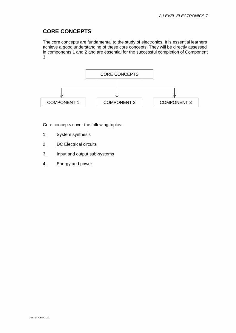
CORE CONCEPTS The core concepts are fundamental to the study of electronics. It is essential learners achieve a good understanding of these core concepts. They will be directly assessed in components 1 and 2 and are essential for the successful completion of Component 3.
CORE CONCEPTS
COMPONENT 1 COMPONENT 2 COMPONENT 3
Core concepts cover the following topics:
1. System synthesis
2. DC Electrical circuits
3. Input and output sub-systems
4. Energy and power
A LEVEL ELECTRONICS 8
© WJEC CBAC Ltd.
1. SYSTEM SYNTHESIS Overview This topic looks at how to represent systems in terms of inputs, processes, outputs and feedback. This will enable complex systems to be represented in terms of sub-systems to allow the communication of complex systems. Electronic skills This topic looks at how learners can describe electronic systems and how complex systems can be broken down into sub-systems. These skills will be used throughout the study of electronics. Learners should be able to: (a) recognise that electronic systems consist of inputs, processes and outputs
and may include feedback
(b) represent complex systems in terms of sub-systems
(c) analyse and design system diagrams.
A LEVEL ELECTRONICS 9
© WJEC CBAC Ltd.
2. DC ELECTRICAL CIRCUITS
Overview This topic covers basic circuit theory. It involves the study of the resistance of an electronic circuit and its relationship with current and potential difference. Resistors and capacitors connected in series and parallel are also explored. Electronic skills This topic gives learners the opportunity to explore electronic circuits through mathematical analysis and practical testing. Learners also develop investigative approaches and practical work, including safe and correct use of equipment and components; keeping records; constructing circuits from circuit diagrams and connecting appropriate measuring instruments. Mathematical skills There are a number of opportunities for the development of mathematical skills in this topic. These include: recognising and using expressions in decimal and standard form; estimating results; using calculators to find reciprocals; using an appropriate number of significant figures; making order of magnitude calculations; and changing the subject of an equation. Learners should be able to: (a) use standard circuit symbols to interpret and draw circuit diagrams
(b) define resistance R, as V
R=I
, describe the effects of resistors in circuits and
be able to use the equation V IR
(c) use the equations to calculate the effective resistance of combinations of resistors connected in series and/or parallel
1 2R R R ... resistors in series
1 2
1 1 1...
R R R resistors in parallel
1 2
1 2
R RR
R R
two resistors in parallel
(d) analyse circuits (based on a single power supply) using Kirchhoff’s laws and
Thevenin’s theorem
(e) select appropriate values of resistor from the E24 series
(f) define capacitance, C as Q
CV

A LEVEL ELECTRONICS 10
© WJEC CBAC Ltd.
(g) explain how capacitors can be used to form the basis of timing circuits and use the equations to calculate the effective capacitance of capacitors in series and parallel
1 2
1 1 1...
C C C capacitors in series
1 2
1 2
CC
C C
C
two capacitors in series
1 2C C C ... capacitors in parallel.
A LEVEL ELECTRONICS 11
© WJEC CBAC Ltd.
3. INPUT AND OUTPUT SUB-SYSTEMS Overview This topic covers how input components can be used to give systems useful information about their environment and the type of outputs the system can control. Electronic skills The topic provides learners with opportunities to explore input devices and their application in sensing using voltage divider circuits through practical testing and mathematical analysis. Learners also develop investigative approaches and practical work, including safe and correct use of equipment and components; keeping records; constructing circuits from circuit diagrams and connecting appropriate measuring instruments. Mathematical skills There are a number of opportunities for the development of mathematical skills in this topic. These include: recognising and using expressions in decimal and standard form; estimating results; using an appropriate number of significant figures; and changing the subject of an equation. Learners should be able to: (a) describe the use of photosensitive devices, ntc thermistors and switches in a
voltage divider circuit to provide analogue signals
(b) determine experimentally, interpret and use characteristic curves for the above devices
(c) use the equation to calculate output voltages for a voltage divider
2
OUT IN
1 2
RV V
R R
(d) explain how a Schmitt inverter can be used to provide signal conditioning
(e) design and construct sensing circuits with photosensitive devices, ntc thermistors and switches
(f) describe the use of a buzzer, a loudspeaker, a motor, a solenoid, a relay; a mechanical actuator (servo) and a seven-segment display in a system.
A LEVEL ELECTRONICS 12
© WJEC CBAC Ltd.
4. ENERGY AND POWER
Overview This topic involves the study of power in DC and AC circuits and the relationship between potential difference, current and power. Electronic skills This topic gives learners the opportunity to explore the power in a circuit through mathematical analysis for DC and AC circuits, with the use of rms (root mean square) voltages and current for an AC circuit. Mathematical skills There are a number of opportunities for the development of mathematical skills in this topic. These include: recognising and using expressions in decimal and standard form; calculating squares and square roots; estimating results; finding arithmetic means; using an appropriate number of significant figures; and changing the subject of an equation. Learners should be able to: (a) recall that power is defined as the rate of doing work and use the relationship
between energy, power and time E Pt
(b) select and apply the rms voltage and current equations, 0
rms
VV
2 and
0
rms
II
2 , including power calculations in a sinusoidal AC circuit
(c) use the power relationships 2
2 VP VI I R
R for AC and DC circuits.
A LEVEL ELECTRONICS 13
© WJEC CBAC Ltd.
2.1 Component 1
Principles of Electronics Written examination: 2 hours 45 minutes 40% of qualification 140 marks This component covers the following topics: 1. Semiconductor components
2. Logic systems
3. Operational amplifiers
4. Signal conversion
5. AC circuits and passive filters
6. Communications systems
7. Wireless transmission
8. Instrumentation systems
A LEVEL ELECTRONICS 14
© WJEC CBAC Ltd.
1. SEMICONDUCTOR COMPONENTS Overview This topic covers the construction of semiconductors in terms of n-type and p-type materials and the processes at a p-n junction and looks at the use of a range of diodes and transistors. Electronic skills The topic gives learners the opportunity to explore the action of several types of diodes and npn bipolar and MOSFET transistors. Learners will also work with various semiconductor devices and calculate values using component data and graphs. Mathematical skills There are a number of opportunities for the development of mathematical skills in this topic. These include: recognising and using expressions in decimal and standard form; estimating results; using an appropriate number of significant figures; changing the subject of an equation; and translating information between graphical, numerical and algebraic forms. Learners should be able to: (a) recall the conduction processes in n- and p-type semiconductors in terms of
electrons and holes
(b) recall conduction processes at a p-n junction, the reasons for the difference in the conducting properties of a p-n diode in the different directions and explain the operation of an LED
(c) recall the principles of operation of a photodiode
(d) explain the properties of an n-channel enhancement mode MOSFET in terms of the effects of bias voltage on the conducting channel (pinching)
(e) describe the use of light-emitting diodes, silicon diodes and zener diodes in electronic systems and using data, including interpreting and sketching characteristic graphs to carry out relevant calculations on circuits containing these devices
(f) calculate series resistor values for LED circuits and select appropriate zener diodes
(g) describe the use of n-channel enhancement mode MOSFETs and npn bipolar transistors in switching circuits, using data to select suitable components for circuits
(h) define gM as the gradient of an ID-VGS graph.

A LEVEL ELECTRONICS 15
© WJEC CBAC Ltd.
(i) select and apply the equations
C FE BI h I bipolar transistor
D M GSI g V( 3) MOSFET
2
D DSonP I r power dissipated in a MOSFET.
A LEVEL ELECTRONICS 16
© WJEC CBAC Ltd.
2. LOGIC SYSTEMS
Overview
This topic involves the study of logic gates in control. Learners will look at the types of logic gates and their function, develop combinations of logic gates to perform other logic functions and to solve set tasks. Methods for simplifying logic systems will also be developed.
Electronic skills
This topic involves learners exploring the use of logic to control systems. Learners will work with different types of logic gates, understand how to connect and combine them to create different functions. They will use several methods to examine the workings of logic systems and be able to simplify these systems.
Mathematical skills
There are a number of opportunities for the development of mathematical skills in this topic. These include: recognising and using expressions in Boolean algebra; simplifying logic systems using Boolean algebra, Karnaugh maps and multiplexers; and translating information between graphical, numerical and algebraic forms.
Learners should be able to:
(a) identify and use NOT; 2 and 3-input AND, NAND, OR, NOR, XNOR and XOR logic gates
(b) construct, recognise and use truth tables for these gates and simple combinations of them
(c) use combinations of one or more types of gate to perform other logic functions including NAND-gate simplification
(d) simplify logic systems using Boolean algebra, Karnaugh maps and multiplexers
(e) design and construct circuits containing logic gates, with consideration to sourcing, sinking, pull-up and pull-down resistors
(f) use de Morgan’s theorem to simplify a logic system
A B A.B
A.B A B
(g) use the Boolean identities
A.1=A, A.0=0, A.A=A, A. A =0, A+1=1, A+0=A, A+ A = A, A+ A =1
(h) select and apply the Boolean identities
A A . B A B
A . B A A . B 1 A
A LEVEL ELECTRONICS 17
© WJEC CBAC Ltd.
3. OPERATIONAL AMPLIFIERS Overview This topic develops the uses of operational amplifiers (op-amps) and how they can be connected for different purposes. It involves the study of gain and outputs calculated from different inputs and resistor values and looks at bandwidth, distortion and slew-rate. Electronic skills This topic gives learners the opportunity to explore the different types of op-amps through modelling or simulation and to compare results to expected estimations and calculated results. Mathematical skills There are a number of opportunities for the development of mathematical skills in this topic. These include: recognising and using expressions in decimal and standard form; understanding and using the symbols: =,<,<<,>>,>,≈,∆; estimating results; using an appropriate number of significant figures; making order of magnitude calculations; translating information between graphical and numerical form; interpreting data presented in graphical form; and changing the subject of an equation.
Learners should be able to: (a) recall the characteristics of an ideal op-amp and be aware that these may be
different for a typical op-amp
(b) recognise that the voltage difference between the two inputs of an op-amp
with negative feedback is virtually zero (resulting in a virtual earth if one of the
inputs is at 0 V) provided the output is not saturated
(c) explain the use of an op-amp in a comparator circuit
(d) recall how the output state of a comparator depends upon the relative values
of the two input states and design comparator switching circuits
(e) recall and apply the conditions for the balance of a bridge circuit
(f) define the voltage gain, G, of an amplifier as OUT
IN
VG
V and be able to select
and apply the equation
(g) draw, recognise and recall the characteristics of the following op-amp circuits:
non-inverting amplifier
inverting amplifier
summing amplifier
comparator
voltage follower circuit
A LEVEL ELECTRONICS 18
© WJEC CBAC Ltd.
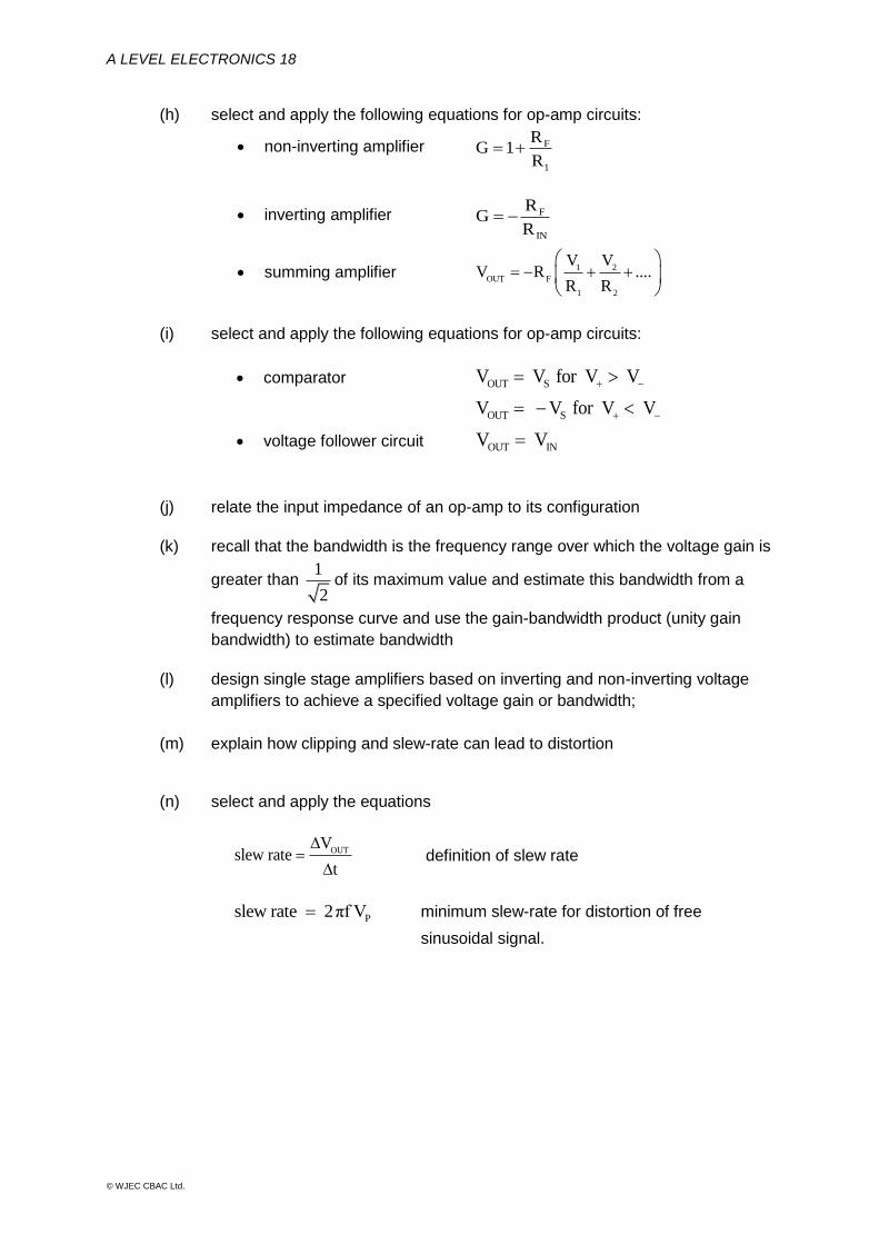
(h) select and apply the following equations for op-amp circuits:
non-inverting amplifier F
1
RG 1
R
inverting amplifier F
IN
RG
R
summing amplifier 1 2
OUT F
1 2
V VV R ....
R R
(i) select and apply the following equations for op-amp circuits:
comparator OUT SV V for V V
OUT SV V for V V
voltage follower circuit OUT INV V
(j) relate the input impedance of an op-amp to its configuration
(k) recall that the bandwidth is the frequency range over which the voltage gain is
greater than 1
2of its maximum value and estimate this bandwidth from a
frequency response curve and use the gain-bandwidth product (unity gain
bandwidth) to estimate bandwidth
(l) design single stage amplifiers based on inverting and non-inverting voltage
amplifiers to achieve a specified voltage gain or bandwidth;
(m) explain how clipping and slew-rate can lead to distortion
(n) select and apply the equations
OUTV
slew ratet
definition of slew rate
P slew rate 2 πf V minimum slew-rate for distortion of free
sinusoidal signal.
A LEVEL ELECTRONICS 19
© WJEC CBAC Ltd.
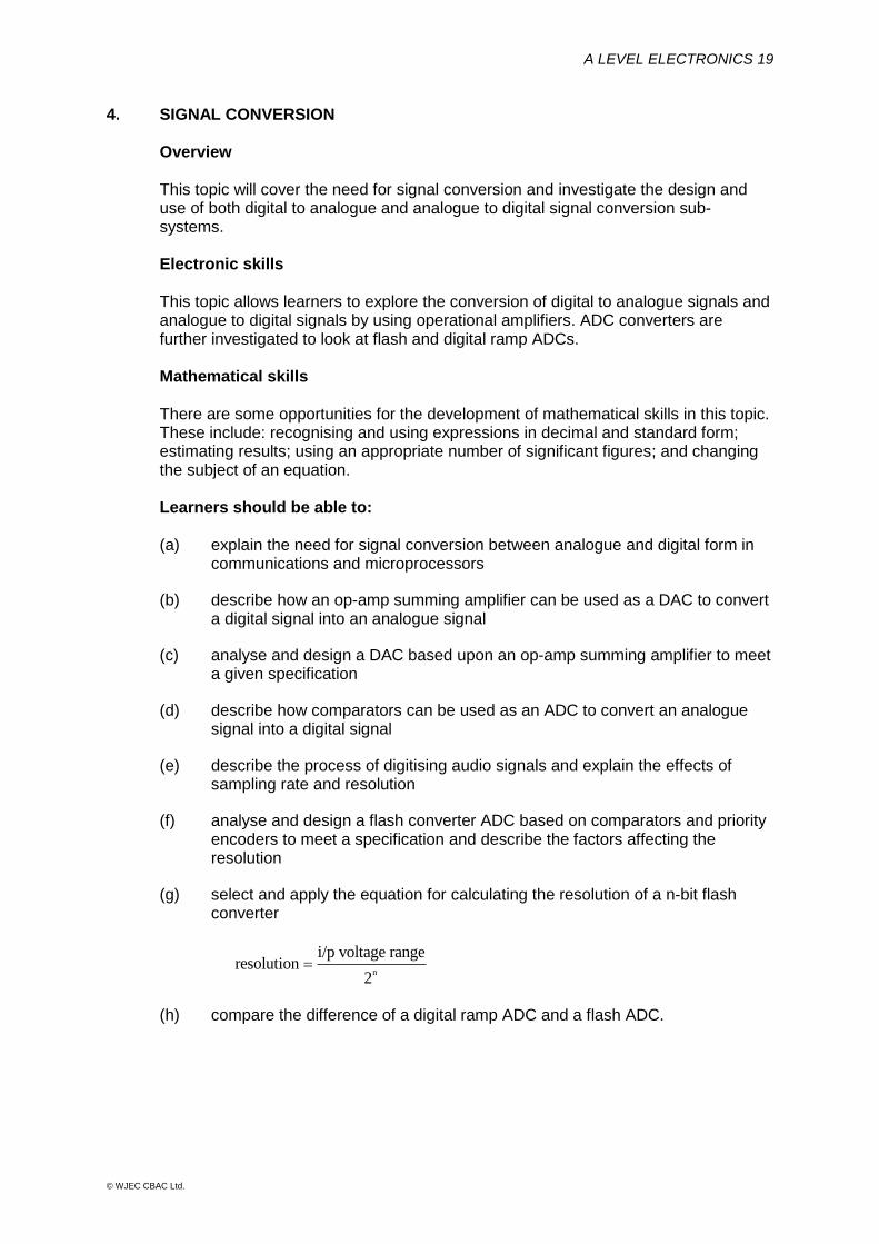
4. SIGNAL CONVERSION Overview This topic will cover the need for signal conversion and investigate the design and use of both digital to analogue and analogue to digital signal conversion sub-systems. Electronic skills This topic allows learners to explore the conversion of digital to analogue signals and analogue to digital signals by using operational amplifiers. ADC converters are further investigated to look at flash and digital ramp ADCs. Mathematical skills There are some opportunities for the development of mathematical skills in this topic. These include: recognising and using expressions in decimal and standard form; estimating results; using an appropriate number of significant figures; and changing the subject of an equation. Learners should be able to: (a) explain the need for signal conversion between analogue and digital form in
communications and microprocessors
(b) describe how an op-amp summing amplifier can be used as a DAC to convert a digital signal into an analogue signal
(c) analyse and design a DAC based upon an op-amp summing amplifier to meet a given specification
(d) describe how comparators can be used as an ADC to convert an analogue signal into a digital signal
(e) describe the process of digitising audio signals and explain the effects of sampling rate and resolution
(f) analyse and design a flash converter ADC based on comparators and priority encoders to meet a specification and describe the factors affecting the resolution
(g) select and apply the equation for calculating the resolution of a n-bit flash converter
n
i/p voltage rangeresolution
2
(h) compare the difference of a digital ramp ADC and a flash ADC.
A LEVEL ELECTRONICS 20
© WJEC CBAC Ltd.
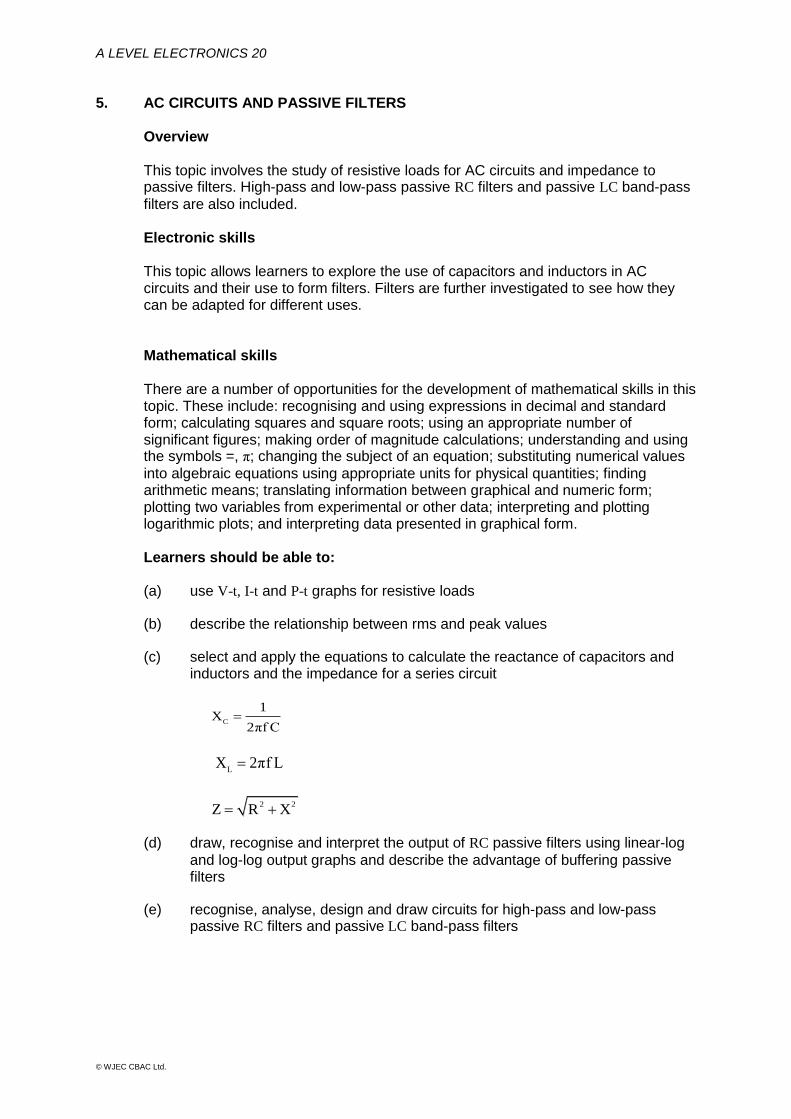
5. AC CIRCUITS AND PASSIVE FILTERS Overview This topic involves the study of resistive loads for AC circuits and impedance to passive filters. High-pass and low-pass passive RC filters and passive LC band-pass
filters are also included. Electronic skills This topic allows learners to explore the use of capacitors and inductors in AC circuits and their use to form filters. Filters are further investigated to see how they can be adapted for different uses. Mathematical skills There are a number of opportunities for the development of mathematical skills in this topic. These include: recognising and using expressions in decimal and standard form; calculating squares and square roots; using an appropriate number of significant figures; making order of magnitude calculations; understanding and using the symbols =, π; changing the subject of an equation; substituting numerical values
into algebraic equations using appropriate units for physical quantities; finding arithmetic means; translating information between graphical and numeric form; plotting two variables from experimental or other data; interpreting and plotting logarithmic plots; and interpreting data presented in graphical form. Learners should be able to: (a) use V-t, I-t and P-t graphs for resistive loads
(b) describe the relationship between rms and peak values
(c) select and apply the equations to calculate the reactance of capacitors and inductors and the impedance for a series circuit
C
1X
2πf C
LX 2πf L
2 2Z R X
(d) draw, recognise and interpret the output of RC passive filters using linear-log
and log-log output graphs and describe the advantage of buffering passive filters
(e) recognise, analyse, design and draw circuits for high-pass and low-pass passive RC filters and passive LC band-pass filters
A LEVEL ELECTRONICS 21
© WJEC CBAC Ltd.
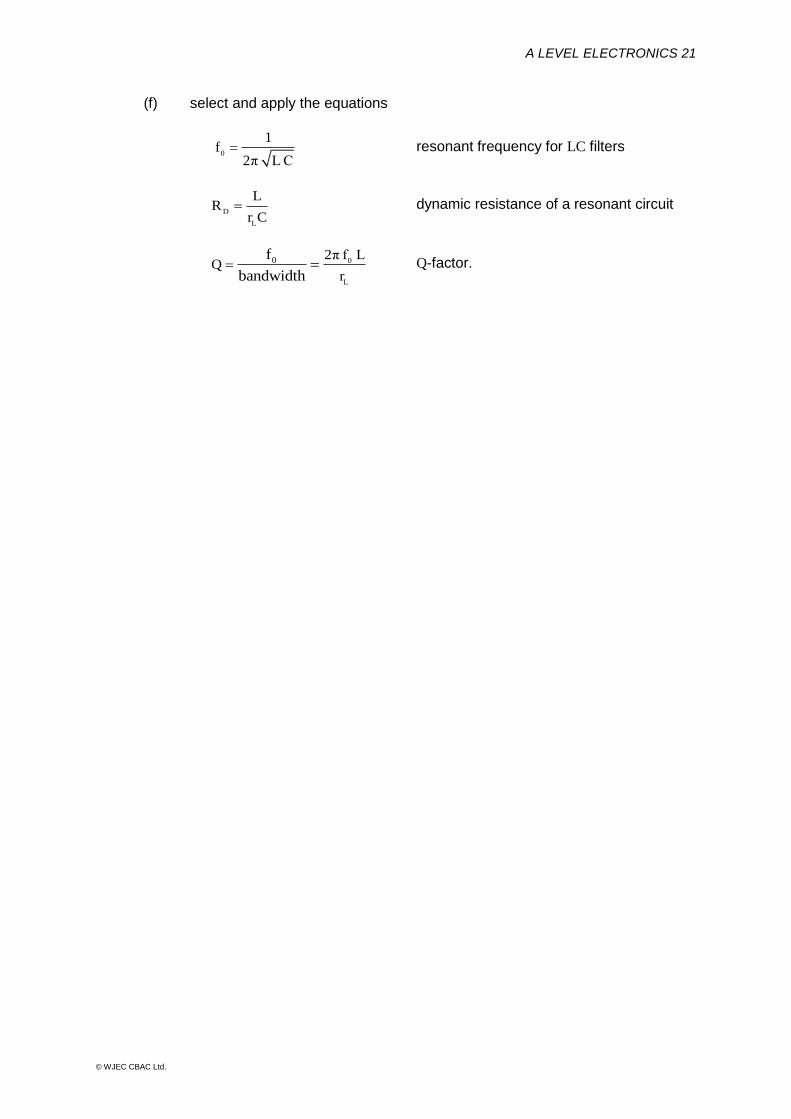
(f) select and apply the equations
0
1f
2π LC
resonant frequency for LC filters
D
L
LR
r C dynamic resistance of a resonant circuit
0
L
0 2π f LQ
r
f
bandwidth
Q-factor.
A LEVEL ELECTRONICS 22
© WJEC CBAC Ltd.
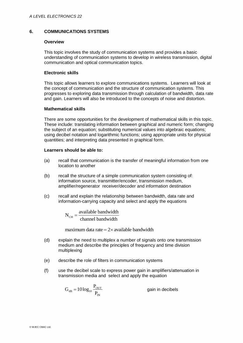
6. COMMUNICATIONS SYSTEMS Overview This topic involves the study of communication systems and provides a basic understanding of communication systems to develop in wireless transmission, digital communication and optical communication topics. Electronic skills This topic allows learners to explore communications systems. Learners will look at the concept of communication and the structure of communication systems. This progresses to exploring data transmission through calculation of bandwidth, data rate and gain. Learners will also be introduced to the concepts of noise and distortion. Mathematical skills There are some opportunities for the development of mathematical skills in this topic. These include: translating information between graphical and numeric form; changing the subject of an equation; substituting numerical values into algebraic equations; using decibel notation and logarithmic functions; using appropriate units for physical quantities; and interpreting data presented in graphical form. Learners should be able to: (a) recall that communication is the transfer of meaningful information from one
location to another
(b) recall the structure of a simple communication system consisting of: information source, transmitter/encoder, transmission medium, amplifier/regenerator receiver/decoder and information destination
(c) recall and explain the relationship between bandwidth, data rate and information-carrying capacity and select and apply the equations
CH
available bandwidthN
channel bandwidth
maximum data rate 2 available bandwidth
(d) explain the need to multiplex a number of signals onto one transmission medium and describe the principles of frequency and time division multiplexing
(e) describe the role of filters in communication systems
(f) use the decibel scale to express power gain in amplifiers/attenuation in transmission media and select and apply the equation
OUTdB 10
IN
PG 10log
P gain in decibels
A LEVEL ELECTRONICS 23
© WJEC CBAC Ltd.
(g) differentiate between noise and distortion
(h) calculate the total gain in a communication system given the power gain or attenuation of its component parts
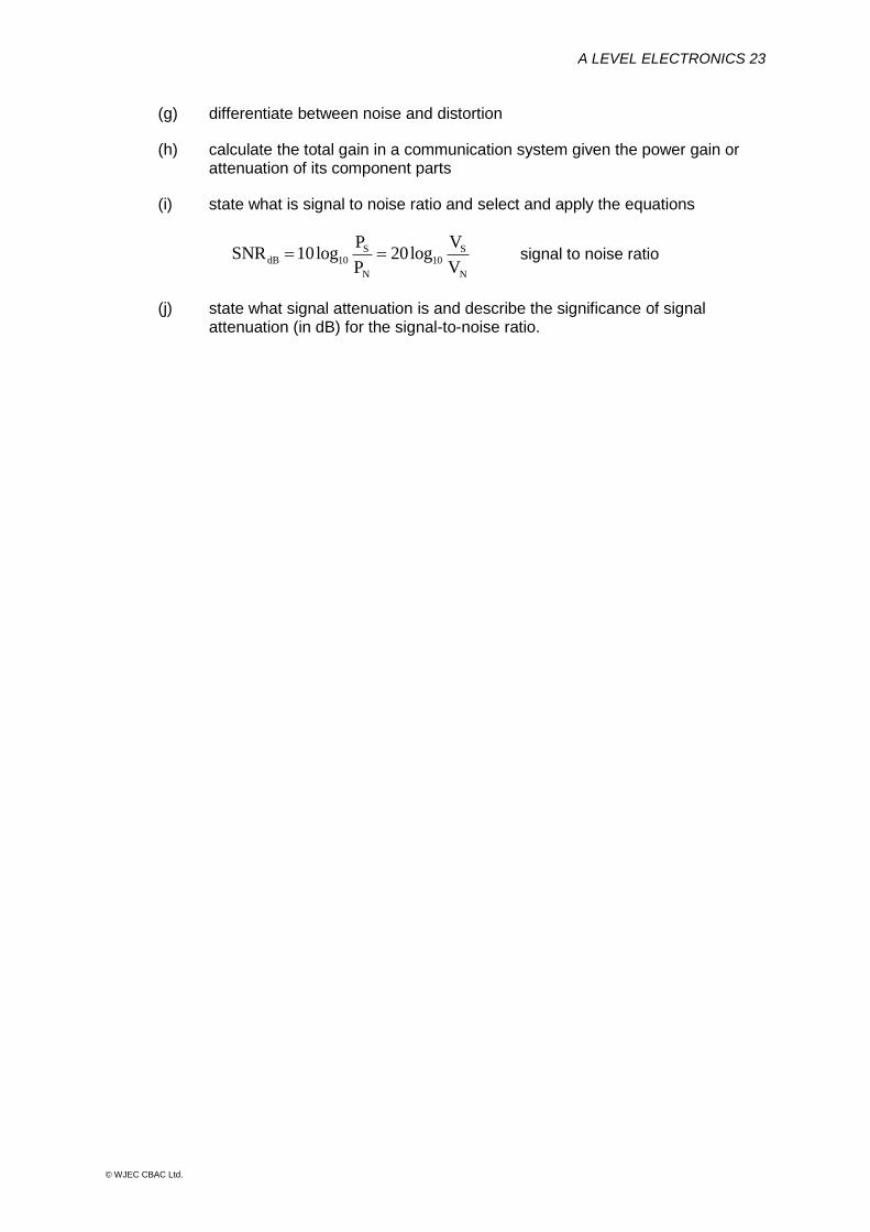
(i) state what is signal to noise ratio and select and apply the equations
S SdB 10 10
N N
P VSNR 10log 20log
P V signal to noise ratio
(j) state what signal attenuation is and describe the significance of signal attenuation (in dB) for the signal-to-noise ratio.
A LEVEL ELECTRONICS 24
© WJEC CBAC Ltd.
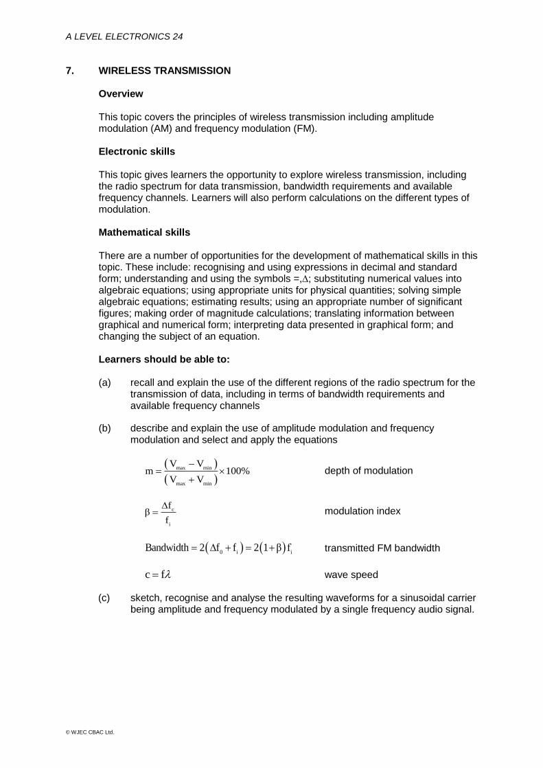
7. WIRELESS TRANSMISSION Overview This topic covers the principles of wireless transmission including amplitude modulation (AM) and frequency modulation (FM). Electronic skills This topic gives learners the opportunity to explore wireless transmission, including the radio spectrum for data transmission, bandwidth requirements and available frequency channels. Learners will also perform calculations on the different types of modulation. Mathematical skills There are a number of opportunities for the development of mathematical skills in this topic. These include: recognising and using expressions in decimal and standard form; understanding and using the symbols =,∆; substituting numerical values into algebraic equations; using appropriate units for physical quantities; solving simple algebraic equations; estimating results; using an appropriate number of significant figures; making order of magnitude calculations; translating information between graphical and numerical form; interpreting data presented in graphical form; and changing the subject of an equation. Learners should be able to: (a) recall and explain the use of the different regions of the radio spectrum for the
transmission of data, including in terms of bandwidth requirements and available frequency channels
(b) describe and explain the use of amplitude modulation and frequency modulation and select and apply the equations
max min
max min
V Vm 100%
V V
depth of modulation
c
i
fβ
f
modulation index
0 i iBandwidth 2 f f 2 1 β f transmitted FM bandwidth
c f wave speed
(c) sketch, recognise and analyse the resulting waveforms for a sinusoidal carrier being amplitude and frequency modulated by a single frequency audio signal.
A LEVEL ELECTRONICS 25
© WJEC CBAC Ltd.
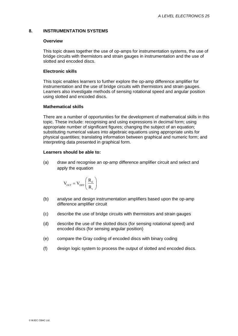
8. INSTRUMENTATION SYSTEMS Overview This topic draws together the use of op-amps for instrumentation systems, the use of bridge circuits with thermistors and strain gauges in instrumentation and the use of slotted and encoded discs. Electronic skills This topic enables learners to further explore the op-amp difference amplifier for instrumentation and the use of bridge circuits with thermistors and strain gauges. Learners also investigate methods of sensing rotational speed and angular position using slotted and encoded discs. Mathematical skills There are a number of opportunities for the development of mathematical skills in this topic. These include: recognising and using expressions in decimal form; using appropriate number of significant figures; changing the subject of an equation; substituting numerical values into algebraic equations using appropriate units for physical quantities; translating information between graphical and numeric form; and interpreting data presented in graphical form.
Learners should be able to: (a) draw and recognise an op-amp difference amplifier circuit and select and
apply the equation
F
OUT DIFF
1
RV V
R
(b) analyse and design instrumentation amplifiers based upon the op-amp difference amplifier circuit
(c) describe the use of bridge circuits with thermistors and strain gauges
(d) describe the use of the slotted discs (for sensing rotational speed) and encoded discs (for sensing angular position)
(e) compare the Gray coding of encoded discs with binary coding
(f) design logic system to process the output of slotted and encoded discs.
A LEVEL ELECTRONICS 26
© WJEC CBAC Ltd.
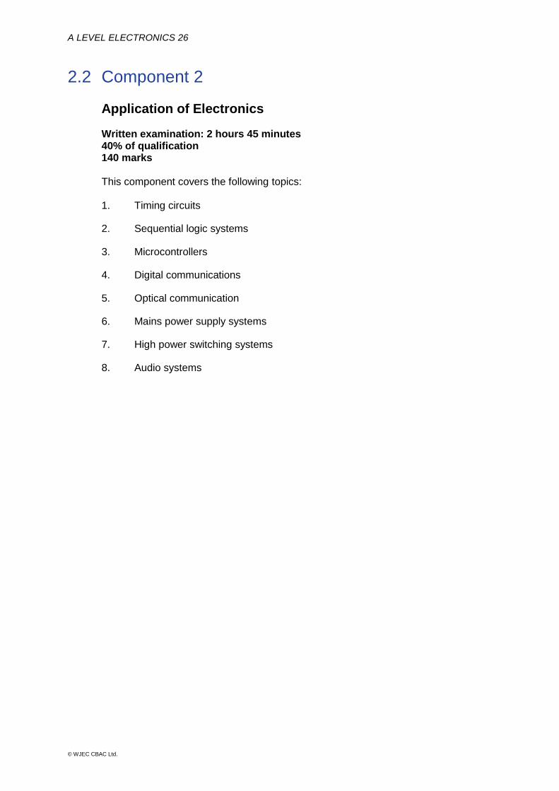
2.2 Component 2
Application of Electronics Written examination: 2 hours 45 minutes 40% of qualification 140 marks This component covers the following topics: 1. Timing circuits
2. Sequential logic systems
3. Microcontrollers
4. Digital communications
5. Optical communication
6. Mains power supply systems
7. High power switching systems
8. Audio systems
A LEVEL ELECTRONICS 27
© WJEC CBAC Ltd.
1. TIMING CIRCUITS Overview This topic develops the use of RC circuits to create time delays and their use in the creation of mono and astable timing circuits. Electronic skills This topic gives learners the opportunities to explore the charging and discharging of a RC network and its application in debouncing switches. Learners also investigate
the operation of a 555 timer IC in monostable and astable circuits through calculation, modelling and simulation. They will also study astable circuits based upon Schmitt triggers. Mathematical skills There are a number of opportunities for the development of mathematical skills in this topic. These include: recognising and using expressions in decimal and standard form; using an appropriate number of significant figures; changing the subject of an equation; substituting numerical values into algebraic equations using appropriate units for physical quantities; using calculators to find and use power, exponential and logarithmic functions; solving simple algebraic equations; translating information between graphical, numeric and algebraic form; plotting two variables from experimental or other data; interpreting and plotting logarithmic plots; interpret data presented in graphical form; and changing the subject of an equation. Learners should be able to:
(a) use the equation for the time constant (T) for an RC circuit: T = RC
(b) select and apply the exponential charging and discharging equations:
t-
RC
C 0V V 1 e
for a charging capacitor
C 0
t
RCV V e
for a discharging capacitor
and use 0.69 RC as the half time and 5 RC as an approximation to estimate
effective charging and discharging times
(c) select and apply the equations
C
0
Vt RCln 1
V
charging capacitor
C
0
Vt RCln
V
discharging capacitor
A LEVEL ELECTRONICS 28
© WJEC CBAC Ltd.
(d) calculate values of T, R and C for a charging / discharging capacitor by using
a graph (including log graphs)
(e) use a RC circuit in debouncing switches
(f) recall the properties of monostable circuits
(g) explain the use of a monostable circuit in conjunction with a RC network in a
time-delay circuit
(h) recall the properties of an astable circuit and its use as a pulse generator
(i) explain the operation, draw and design the circuit of an astable circuit based
upon a Schmitt trigger and select and apply the approximation1
fRC
, where
f is the operating frequency
(j) draw and analyse circuits for monostable and astable circuits based upon a 555 timer IC, and select and apply the following equations to calculate their characteristics including pulse duration, frequency, mark-space ratio
1f
T frequency, period relationship
T 1.1RC 555 monostable
H 1 2t 0.7 R R C mark time of a 555 astable circuit
L 2t 0.7R C space time of a 555 astable circuit
1 2
1.44f
R 2R C
frequency of a 555 astable circuit
ON 1 2
OFF 2
T R R
T R
mark/space ratio of an astable.
A LEVEL ELECTRONICS 29
© WJEC CBAC Ltd.
2. SEQUENTIAL LOGIC SYSTEMS
Overview
This topic covers latches based on NAND gates and propagation delays in sequential systems. It involves the study of characteristics and uses for a range of systems based on D-type flip-flops, dedicated 4-bit counters, 2 digit decimal counter and synchronous counter systems.
Electronic skills
This topic expands on the logic systems topic, which gives learners further opportunities to design and analyse sequential logic systems. Learners will also explore a range of uses for D-type flip-flops.
Mathematical skills
There are a number of opportunities for the development of mathematical skills in this topic. These include: recognising and using expressions in Boolean algebra; simplifying logic systems using Boolean algebra, Karnaugh maps and multiplexers; translating information between graphical, numerical and algebraic forms, constructing and using timing diagrams; and converting between binary, decimal, hexadecimal and binary-coded decimal (BCD) number systems.
Learners should be able to:
(a) design and describe the action of a Set-Reset (SR ) latch based on NAND
gates
(b) describe the significance of propagation delays in sequential systems
(c) construct and use timing diagrams to explain the operation of sequential logic circuits
(d) recall the characteristics and uses of the inputs and outputs of D-type flip-flops for:
transition gates
frequency divider circuits
asynchronous counters
parallel-in-series-out (PISO) registers
series-in-parallel-out (SIPO) registers
synchronous counters
(e) design systems that use a dedicated 4-bit counter and combinational logic to produce a sequence of events
(f) design and analyse a 2 digit decimal counting system
(g) convert between binary, decimal, hexadecimal and binary-coded decimal (BCD) number systems
(h) design sequence generators based on D-type flip-flops configured as synchronous counters, use state diagrams and explain the significance of stuck and unused states, including Boolean manipulation to produce simpler solutions.
A LEVEL ELECTRONICS 30
© WJEC CBAC Ltd.
3. MICROCONTROLLERS Overview This topic covers the microcontroller as a programable integrated circuit (PIC) and its internal structure. It also covers how microcontrollers are interfaced and programed through flowcharts and assembler language to perform tasks.
Electronic skills
Learners will have the opportunity in this topic to work with microcontrollers, interfacing them to inputs and outputs and programing them to perform set tasks. Learners will also use both flowcharts and assembler language to program the microcontrollers and look at the application of microcontrollers.
Mathematical skills
There are some opportunities for the development of mathematical skills in this topic. These include: converting between binary and decimal number systems; and drawing and interpreting flowcharts. Learners should be able to: (a) analyse and design flowchart programs to program microcontrollers
(b) recall and describe the structure of a PIC microcontroller as programmable assemblies of memory, input ports, output ports, CPU, clock and reset
(c) recall and explain the use of interrupts to allow an external device to be serviced on request
(d) recall and describe the application of a PIC microcontroller
(e) analyse, design and program PIC microcontroller-based circuits using assembler language.
A LEVEL ELECTRONICS 31
© WJEC CBAC Ltd.
4. DIGITAL COMMUNICATIONS Overview This topic develops the concepts of digital communication by examining different types of modulation and the regeneration of digital signals. Block diagrams of pulse code modulation (PCM) systems are used to explain their operation. Also Nyquist theorem and time division multiplexing (TDM) is introduced. Electronic skills This topic enables learners to explore the construction of systems required for digital communications. They will also have opportunity to explore parts of digital communication systems. Mathematical skills There are some opportunities for the development of mathematical skills in this topic. These include: translating information between graphical and numeric form; plotting two variables from data; and interpreting data presented in graphical form Learners should be able to: (a) analyse and design Schmitt trigger circuits to regenerate a digital signal
(b) analyse and draw graphs to illustrate pulse modulation techniques (pulse width modulation (PWM), pulse amplitude modulation (PAM), pulse position modulation (PPM))
(c) draw a block diagram for and describe the operation of a pulse code modulation (PCM) communication system consisting of:
transmitter low pass filter, sampling gate, sampling clock, ADC, PISO shift register, PISO clock
and receiver Schmitt trigger, SIPO shift register, SIPO clock, DAC, low pass filter
(d) use the relationship between required sampling frequency to the highest frequency in the signal and Nyquist theorem
(e) describe how time division multiplexing (TDM) can be used to improve the user capacity of a PCM communications link
(f) state the limitation on the number of channels that can be incorporated into a PCM communications link, using TDM and use given data to calculate how many channels can be incorporated into a PCM communications link, using TDM.
A LEVEL ELECTRONICS 32
© WJEC CBAC Ltd.
5. OPTICAL COMMUNICATION Overview This topic introduces the principles of optical communication, its limitations and the principles for converting between electrical and optical signals. Electronic skills Learners will have the opportunity to study optical communications, with practical opportunities to explore basic circuits for converting between electrical and optical signals by modelling the systems. Learners should be able to: (a) describe how the refractive properties of glass allow signals to be transmitted
over long distances in optical fibres
(b) describe the effects of dispersion, attenuation and radiation losses in optical fibre communication and the relative advantages of single and multi-mode optical fibres in a communication network
(c) describe the principles of operation of circuits for converting between electrical and optical signals
(d) describe the use of LED and laser light sources in an optical fibre transmitter.
A LEVEL ELECTRONICS 33
© WJEC CBAC Ltd.
6. MAINS POWER SUPPLY SYSTEMS Overview This topic explores power supplies with half and full wave rectification, the use of capacitors and load and line regulation. The topic also involves the analysis and design of regulators based upon a zener diode, a transistor emitter follower and a non-inverting amplifier. Electronic skills This topic gives learners opportunities to model and simulate half and full wave rectification, by examining the effect of capacitors and loads on the output of simple power supplies. Learners have the opportunity to construct and test a range of voltage regulators consisting of a zener diode, a transistor emitter follower or non-inverting amplifier. Mathematical skills There are a number of opportunities for the development of mathematical skills in this topic. These include: recognising and using expressions in decimal and standard form; using an appropriate number of significant figures; making order of magnitude calculations; changing the subject of an equation; translating information between graphical and numerical form; and interpreting data presented in graphical form. Learners should be able to: (a) recall the use of diodes for half-wave and full wave rectification
(b) describe the effect of capacitors and loads on the output of a simple power supply
(c) select and apply the ripple voltage equation
r
r
IV
f C
(d) design zener regulated power supplies and draw graphs to show the effect of loading
(e) distinguish between load regulation and line regulation
(f) analyse and design a voltage regulator based upon a zener diode, a transistor emitter follower and a non-inverting amplifier
(g) select and apply the gain equation
F
L Z
1
RV V 1
R
A LEVEL ELECTRONICS 34
© WJEC CBAC Ltd.
7. HIGH POWER SWITCHING SYSTEMS Overview This topic involves the study of high power switching for both DC/AC loads. It covers the use and application of thyristors, diacs and triacs for high power switching. Electronic skills This topic gives opportunities for learners to model and simulate switching circuits for both DC and AC systems. Mathematical skills There are a number of opportunities for the development of mathematical skills in this topic. These include: recognising and using expressions in decimal and standard
form; using calculators to find and use power, exponential and tan functions;
estimating results; using an appropriate number of significant figures; making order of magnitude calculations; changing the subject of an equation; translating information between graphical and numerical form; and interpret data presented in graphical form. Learners should be able to: (a) describe the advantages of using thyristors and triacs to switch high power
DC/AC loads respectively, compared to using a transistor or a relay
(b) recall the general thyristor characteristics, the conditions under which a thyristor conducts and explain the significance of the following terms:
holding current, minimum gate voltage, minimum gate current
(c) design DC thyristor switching circuits and explain the process of capacitor commutation
(d) draw the circuit diagram and analyse graphs for an AC phase control circuit, using a RC network, a triac and a diac
(e) select and apply the equation
1
C
Rtan
X
to calculate the phase shift between supply voltage and capacitor voltage.
A LEVEL ELECTRONICS 35
© WJEC CBAC Ltd.
8. AUDIO SYSTEMS Overview This topic develops the use of amplifier and filter sub-systems to construct audio systems. Electronic skills This topic develops ideas studied in earlier topics and involves the use of amplifiers and filters in practical situations for audio systems. Learners will have opportunity to investigate through calculations, modelling and simulation a range of amplifier circuits based on a multi-stage voltage preamplifier, summing amplifier, emitter and source follower power amplifiers, push-pull power amplifiers including active filters. Mathematical skills There are a number of opportunities for the development of mathematical skills in this topic. These include: recognising and using expressions in decimal and standard form; understanding and using the symbols: =,≈; estimating results; using an appropriate number of significant figures; making order of magnitude calculations; changing the subject of an equation; translating information between graphical and numerical form; and interpreting data presented in graphical form. Learners should be able to: (a) recall the structure of a simple audio system based upon preamplifiers, a
mixer, tone controls, a power amplifier and output loudspeaker
(b) analyse and design a multi-stage voltage preamplifier to meet bandwidth and gain requirements
(c) analyse and design a mixer circuit based upon a summing amplifier
(d) describe and explain the operation of first order active filters (bass boost, treble boost, bass cut, treble cut) based upon an op-amp inverting amplifier and select and apply the equation to calculate the break frequency
b
1f
2π R C
(e) recall and apply the maximum power transfer theorem
(f) draw circuits for and recall the properties of emitter and source follower power
amplifiers ( OUT INV V 0.7 for an emitter follower and OUT INV V 3 for
source follower)

A LEVEL ELECTRONICS 36
© WJEC CBAC Ltd.
(g) draw circuits for and recall the properties of push-pull power amplifiers consisting of either emitter or source followers and select and apply the equation
2
S
MAX
L
VP
8R push-pull power amplifier
(h) analyse and draw graphs of the waveforms for first order active filters, emitter and source follower power amplifiers and push-pull power amplifiers
(i) describe cross over distortion in push-pull amplifiers and its removal using negative feedback.
A LEVEL ELECTRONICS 37
© WJEC CBAC Ltd.
2.3 Component 3
Extended system design and realisation tasks Non-exam assessment (NEA) 20% of qualification 70 marks The NEA is an integral part of the WJEC Eduqas A level in Electronics and contributes 20% to the final assessment. This component requires each learner to complete two tasks independently. The tasks build on the concepts studied throughout the specification and the requirements to relate practical circuit design and realisation to knowledge and understanding gained from the study of components 1 and 2. Task 1 (20 marks) – involves the development of a microcontroller system programed through assembler language. Task 2 (50 marks) – is a substantial system development including analogue and digital sub-systems in an integrated design. Each task enables learners to carry out a design and realisation task based on an individually identified problem, context or opportunity. This will be researched and analysed by the learner to develop their own specification to clearly guide their system development. Learners will develop their system from a series of sub-systems which will be tested individually before assembly and testing as a complete system. Learners must evaluate the performance of their developed system against their specification and suggest improvements that could be made. This component requires learners, in the context of the knowledge and understanding in Components 1 and 2, to demonstrate their ability to:
(a) analyse a problem1 to enable solutions to be developed
(b) develop a design specification to solve a problem
(c) propose an electronic system, composed of sub-systems, to satisfy a design specification
(d) make predictions about the way that electronic systems behave
(e) design and build an electronic system, modelling its performance against the design specification, modifying as appropriate
(f) plan tests to make measurements, to explore a problem, selecting appropriate techniques and instruments
(g) evaluate practical risks in system development and application
1 In the context of A level electronics skills, 'problem' is interpreted broadly, to embrace:
problem – difficulties in a situation e.g. a person with partial hearing cannot hear the doorbell
context – looking at situations for possible design openings e.g. a person crossing the road
opportunity – possibilities arising e.g. from a new improved component
A LEVEL ELECTRONICS 38
© WJEC CBAC Ltd.
(h) carry out tests having due regard to the correct manipulation of apparatus, accuracy of measurement and Health and Safety considerations
(i) make and record measurements on electrical circuits
(j) report results using standard scientific conventions
(k) evaluate the performance of the electronic system against the design specification
(l) suggest improvements to the electronic system following evaluation
(m) design a microcontroller system; programming the microcontroller using assembly language (Task 1 only)
Learners should be encouraged and supported to select tasks in which they are interested and which are neither under nor over ambitious. The focus for each of the learner's tasks must be signed off by the teacher. The teacher should discuss the proposed focus of the task with the learner, considering the requirements of the assessment and the ability and interests of the individual learner. The teacher must be satisfied that the suggested focus has the potential for the individual learner to:
analyse the problem and derive a design specification;
develop and test a range of sub-systems;
develop, realise and test a final physical system;
evaluate the final system against the design specification and suggest improvements.
This will help ensure the task is at a suitable level for the learner concerned and will provide that individual with a level of challenge that is appropriate to their abilities, in the context of the requirements of an A level Electronics qualification. Task 1
Task 1 is intended to introduce learners to software control techniques using assembly language which is widely used to program microcontrollers for consumer products. It is not expected that learners will be familiar with every instruction in the instruction set, or use every programming technique available. Several manufacturers produce PIC development systems which can be used to deliver this part of the component. The work should not be limited to 'onscreen' design and emulation, but must involve the actual programing of a PIC chip, and its testing remotely on a physical circuit. Initial program testing can be carried out using a development board to prove the program works before final testing on a physical circuit.
The report must include a listing of the program, a description of how the program works and testing of the program
Task 2
Once the learner has decided on a context for the task, they should undertake appropriate research so that a list of performance parameters (specification) can be given. It is expected that the design specification will contain realistic numerical values against which the final performance of the system can be judged.
In each task the overall system should be developed as a number of sub-systems which should be individually tested and evaluated before being incorporated into the
A LEVEL ELECTRONICS 39
© WJEC CBAC Ltd.
complete system. This will ensure that the complete system develops by a gradual and incremental process, having been assessed at each stage of its development.
For microcontroller-based projects, a sub-routine can be considered as a sub-system provided its specification can be tested and evaluated in a similar fashion to a component-based sub-system. To meet the assessment requirements, a microcontroller-based project will also need to include, as a minimum, some component-based processing sub-systems for interfacing signals to and from the microcontroller (in addition to the microcontroller circuitry).
In each task the system should be fully tested when the project is complete. The testing should be documented with results being displayed in tables and graphs, where appropriate. These tests will enable the learner to assess the system and identify any faults and limitations. The learner should attempt to modify the system to correct for any limitations and then produce a final set of performance figures for the completed system. The learner should then evaluate the final system against the design specification and suggest further developments.
The learner should fully document the development of each task in a report. It is the evidence contained within this report and the system produced upon which the NEA should be marked and assessed. The report should contain evidence for each task of the following sections:
System planning – including analysis of the problem and a design specification
System development – including the development of the system in terms of sub-systems, annotated circuit diagrams and description of testing each sub-system and the recording of results
System realisation – including annotated block and circuit diagrams; evidence of layout planning; description of testing of complete systems and the recording of results and user guide
Evaluation – including a detailed evaluation of the system against the design specification and suggestions for improvement.
The report should be presented in a logical order that is clearly presented and easy to understand. It should contain an acknowledgement of all sources of information and help. Photographs of the complete physical system must be included in the report.
Physical circuit
Construction of both systems may be on prototype board, strip board or printed circuit board. Whichever method of construction is chosen, the layout and mounting of components and wiring should be neat and logical, assist the design, allow testing of and fault finding of the system. Pre-constructed circuit boards such as PIC or Arduino development boards are not acceptable as the final circuit.
Supervision
The tasks must be appropriately supervised to ensure that teachers are able to confidently authenticate each learner’s work. Learners are allowed supervised access to resources that may include information gathered outside supervised time. Each learner must produce their NEA under immediate supervision.
A LEVEL ELECTRONICS 40
© WJEC CBAC Ltd.
Each learner must produce their system under 'immediate supervision'. This means the system has to be produced either:
(i) with the simultaneous physical presence of the learner and the supervisor,
or (ii) remotely by means of simultaneous electronic communication.
In most cases supervision will be of the form described in (i), but in some circumstances, for example if the learner is carrying out a specialist process away from the centre, (ii) may be more appropriate. Appendix D gives guidance on the level of independence in NEA tasks. Time allocation
The NEA is integral to WJEC Eduqas A level Electronics and contributes 20% to the final assessment. Time is not prescribed for this work because the process of the learner's independent design and realisation tasks are iterative. They include the design, prototyping, testing and evaluating of sub-systems and systems, alongside the writing of the task reports. Learners should seek guidance from their teachers and engage as necessary in learner-led discussions. Teachers should make time available for the following:
to explain the requirements of the independent design and construction task
to guide learners to an appropriate context
to direct learners to the assessment objectives relevant to the assessment of the component
to analyse Health and Safety considerations and the risk assessment of practical work.
As a consequence, the overall time allocated to the independent design and realisation tasks both by teacher and learners should be commensurate with a 20% weighting of the whole qualification for this component.
A LEVEL ELECTRONICS 41
© WJEC CBAC Ltd.
3 ASSESSMENT
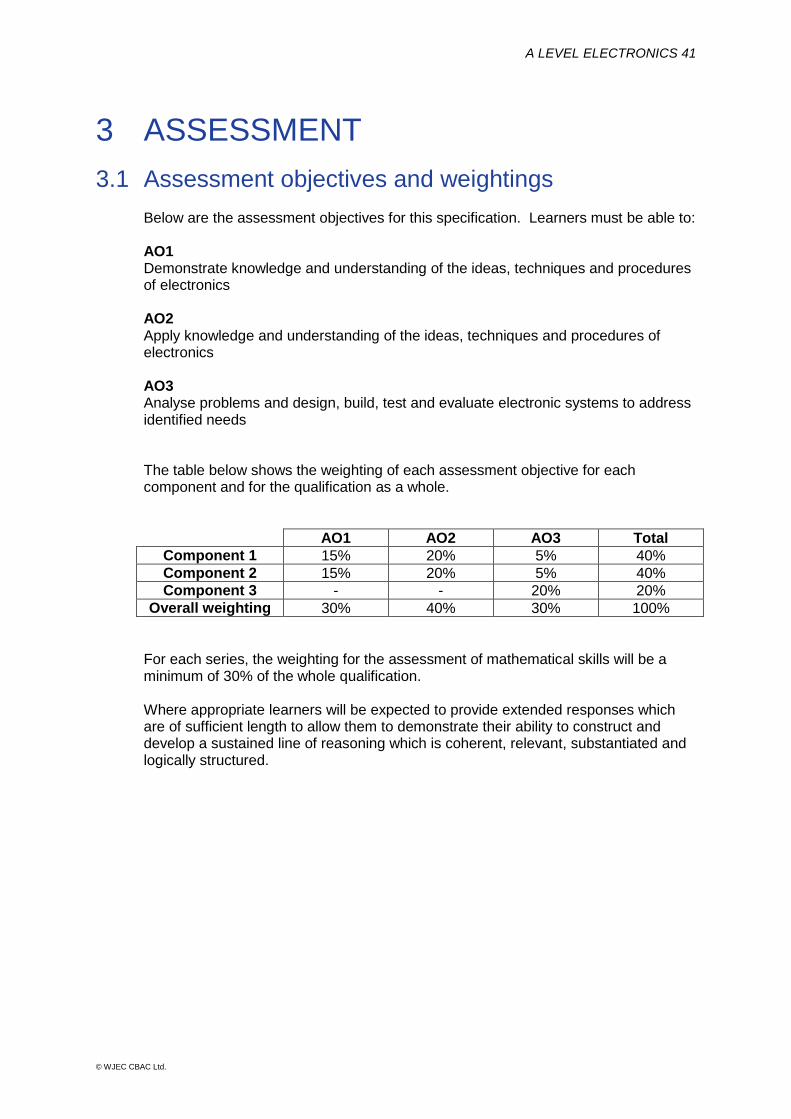
3.1 Assessment objectives and weightings Below are the assessment objectives for this specification. Learners must be able to: AO1 Demonstrate knowledge and understanding of the ideas, techniques and procedures of electronics AO2 Apply knowledge and understanding of the ideas, techniques and procedures of electronics AO3 Analyse problems and design, build, test and evaluate electronic systems to address identified needs The table below shows the weighting of each assessment objective for each component and for the qualification as a whole.
AO1 AO2 AO3 Total
Component 1 15% 20% 5% 40%
Component 2 15% 20% 5% 40%
Component 3 - - 20% 20%
Overall weighting 30% 40% 30% 100%
For each series, the weighting for the assessment of mathematical skills will be a minimum of 30% of the whole qualification. Where appropriate learners will be expected to provide extended responses which are of sufficient length to allow them to demonstrate their ability to construct and develop a sustained line of reasoning which is coherent, relevant, substantiated and logically structured.
A LEVEL ELECTRONICS 42
© WJEC CBAC Ltd.
3.2 Arrangements for non-exam assessment
Marking of extended system design and realisation tasks
Marks should be awarded for the criteria listed in the assessment grids for non-exam assessment (see Appendix E).
Exemplification statements are given in the mark grid to indicate the features which should be present in a candidate’s work to be awarded full marks for that section and the level. A 'level of response' mark scheme is used. The relevant section(s) of the candidate's work should be read from start to finish before applying the mark scheme. Then the work should be matched to the level descriptors to decide which descriptor matches best with the candidate’s work, whilst remembering to consider the overall quality of the response. Next, which mark to award within the band needs to be determined. If there is a good match with the content (and, where relevant, the communication statements for QER) then the highest mark for the band should be awarded. Lower marks within the band should be awarded for proportionately weaker matches with the content for the band. It is the responsibility of the centre to ensure the authenticity of all work presented for assessment. All candidates are required to sign an authentication statement endorsing the originality of their work presented for assessment, and assessors must countersign that they have taken all reasonable steps to validate this. Authentication documentation must be completed by all candidates, not just those selected for moderation. Marks should only be awarded for work which is that of the candidate. Any assistance that goes beyond general guidance must be recorded on the Electronics task form and taken into account when marking the work. Marks should only be awarded when there is supporting evidence. Supervisors must annotate each candidate's Electronics task form and/or the relevant section of the work to identify the location of relevant evidence. Annotation should also be provided to indicate to what degree the final performance met the initial specification. For each task the candidate's report must contain clear photographic evidence of the completed circuit. The centre is responsible for carrying out internal standardisation where two or more teachers have been involved in the marking of the work submitted for a single unit.
Moderation of NEA Once the centre has marked all candidates’ work, the marks must be entered into the online system for each individual and sent electronically to WJEC. The online system will then select and return the candidates identified for the moderation sample. For each candidate in the sample, the moderator must be sent a completed Electronics task form with the task reports and photographic evidence of the completed physical systems. The Electronics task form will be available on the WJEC website.
A LEVEL ELECTRONICS 43
© WJEC CBAC Ltd.
4 TECHNICAL INFORMATION
4.1 Making entries This is a linear qualification in which all assessments must be taken at the end of the course. Assessment opportunities will be available in May/June each year, until the end of the life of this specification. Summer 2019 will be the first assessment opportunity. Where learners wish to re-sit the qualification, all components must be re-taken. The entry code appears below. WJEC Eduqas A level Electronics: A490QS The current edition of our Entry Procedures and Coding Information gives up-to-date entry procedures.
4.2 Grading, awarding and reporting A level qualifications are reported as a grade from A* to E. Results not attaining the minimum standard for the award will be reported as U (unclassified).
A LEVEL ELECTRONICS 44
© WJEC CBAC Ltd.
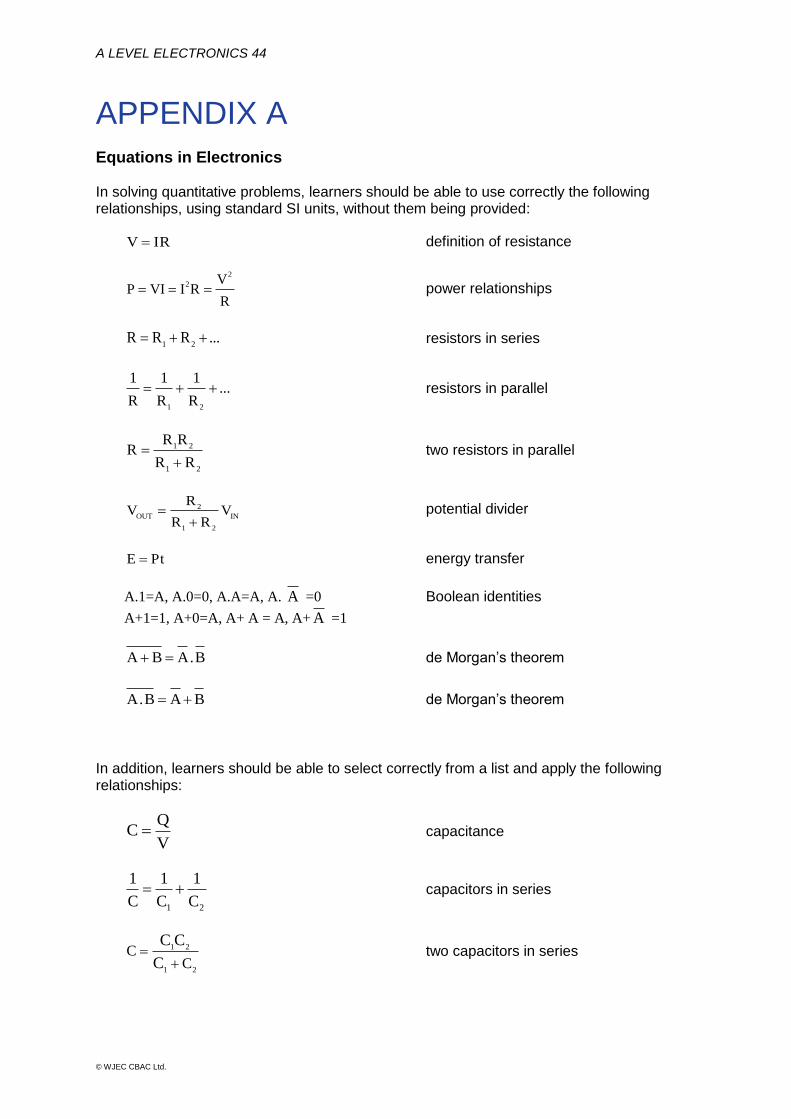
APPENDIX A
Equations in Electronics In solving quantitative problems, learners should be able to use correctly the following relationships, using standard SI units, without them being provided:
V IR definition of resistance
2
2 VP VI I R
R power relationships
1 2R R R ... resistors in series
1 2
1 1 1...
R R R resistors in parallel
1 2
1 2
R RR
R R
two resistors in parallel
2
OUT IN
1 2
RV V
R R
potential divider
E Pt energy transfer
A.1=A, A.0=0, A.A=A, A. A =0 Boolean identities
A+1=1, A+0=A, A+ A = A, A+ A =1
A B A.B de Morgan’s theorem
A.B A B de Morgan’s theorem
In addition, learners should be able to select correctly from a list and apply the following relationships:
QC
V capacitance
1 2
1 1 1
C C C capacitors in series
1 2
1 2
CC
C C
C
two capacitors in series
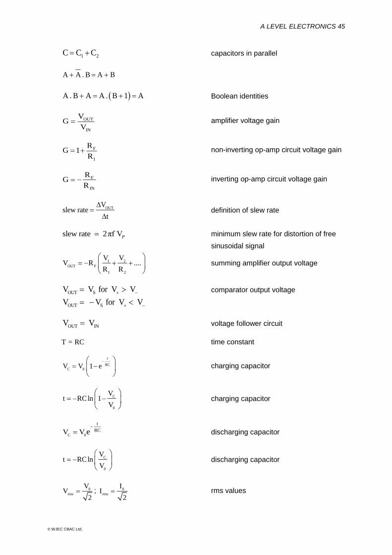
A LEVEL ELECTRONICS 45
© WJEC CBAC Ltd.
1 2C C C capacitors in parallel
A A . B A B
A . B A A . B 1 A Boolean identities
OUT
IN
VG
V amplifier voltage gain
F
1
RG 1
R non-inverting op-amp circuit voltage gain
F
IN
RG
R inverting op-amp circuit voltage gain
OUTV
slew ratet
definition of slew rate
slew rate 2 πf VP minimum slew rate for distortion of free
sinusoidal signal
1 2
OUT F
1 2
V VV R ....
R R
summing amplifier output voltage
OUT SV V for V V comparator output voltage
OUT SV V for V V
OUT INV V voltage follower circuit
T = RC time constant
t-
RC
C 0V V 1 e
charging capacitor
C
0
Vt RCln 1
V
charging capacitor
C 0
t
RCV V e
discharging capacitor
C
0
Vt RCln
V
discharging capacitor
0
rms
VV
2 ; 0
rms
II
2 rms values
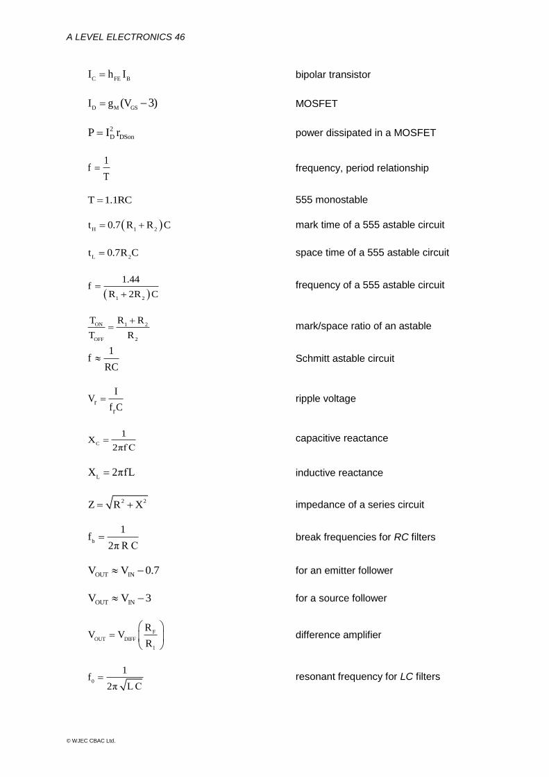
A LEVEL ELECTRONICS 46
© WJEC CBAC Ltd.
C FE BI h I bipolar transistor
D M GSI g V( 3) MOSFET
2
D DSonP I r power dissipated in a MOSFET
1f
T frequency, period relationship
T 1.1RC 555 monostable
H 1 2t 0.7 R R C mark time of a 555 astable circuit
L 2t 0.7R C space time of a 555 astable circuit
1 2
1.44f
R 2R C
frequency of a 555 astable circuit
ON 1 2
OFF 2
T R R
T R
mark/space ratio of an astable
1f
RC Schmitt astable circuit
r
r
IV
f C ripple voltage
C
1X
2πf C
capacitive reactance
L
X 2πfL inductive reactance
2 2Z R X impedance of a series circuit
b
1f
2π R C
break frequencies for RC filters
OUT INV V 0.7 for an emitter follower
OUT INV V 3 for a source follower
F
OUT DIFF
1
RV V
R
difference amplifier
0
1f
2π LC
resonant frequency for LC filters
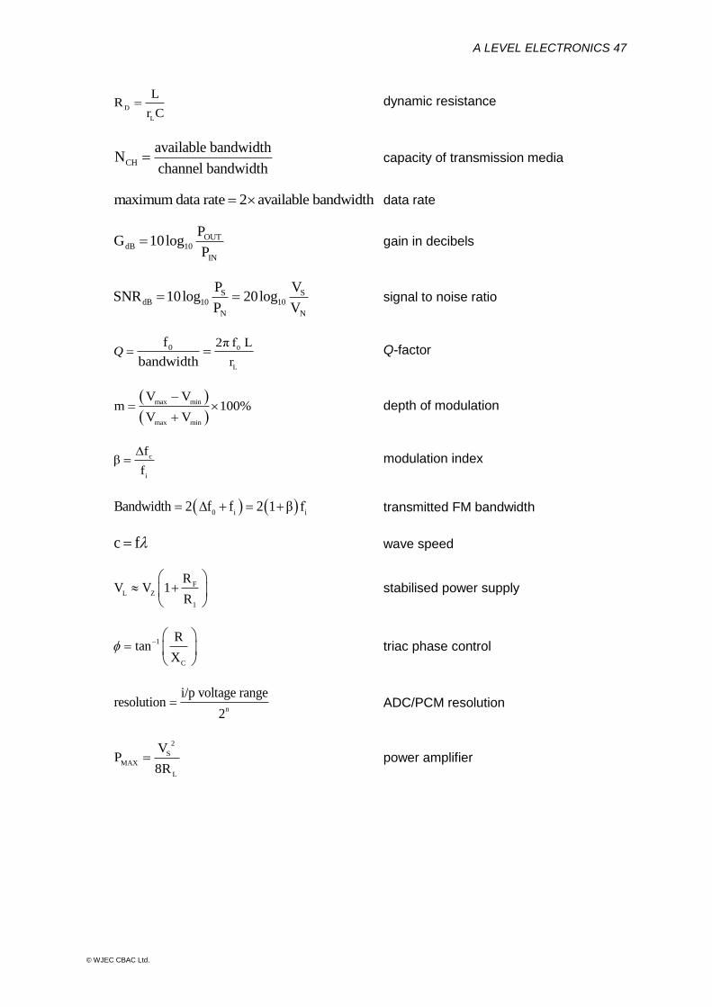
A LEVEL ELECTRONICS 47
© WJEC CBAC Ltd.
D
L
LR
r C dynamic resistance
CH
available bandwidthN
channel bandwidth capacity of transmission media
maximum data rate 2 available bandwidth data rate
OUTdB 10
IN
PG 10log
P gain in decibels
S SdB 10 10
N N
P VSNR 10log 20log
P V signal to noise ratio
0
L
0 2π f L
r
f
bandwidthQ
Q-factor
max min
max min
V Vm 100%
V V
depth of modulation
c
i
fβ
f
modulation index
0 i iBandwidth 2 f f 2 1 β f transmitted FM bandwidth
c f wave speed
F
L Z
1
RV V 1
R
stabilised power supply
1
C
Rtan
X
triac phase control
n
i/p voltage rangeresolution
2 ADC/PCM resolution
2
S
MAX
L
VP
8R power amplifier
A LEVEL ELECTRONICS 48
© WJEC CBAC Ltd.
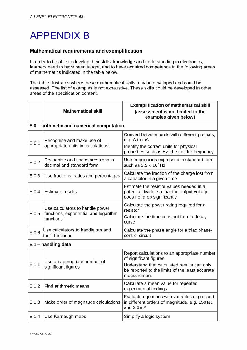
APPENDIX B Mathematical requirements and exemplification In order to be able to develop their skills, knowledge and understanding in electronics, learners need to have been taught, and to have acquired competence in the following areas of mathematics indicated in the table below. The table illustrates where these mathematical skills may be developed and could be assessed. The list of examples is not exhaustive. These skills could be developed in other areas of the specification content.
Mathematical skill
Exemplification of mathematical skill
(assessment is not limited to the examples given below)
E.0 – arithmetic and numerical computation
E.0.1 Recognise and make use of appropriate units in calculations
Convert between units with different prefixes, e.g. A to mA
Identify the correct units for physical properties such as Hz, the unit for frequency
E.0.2 Recognise and use expressions in decimal and standard form
Use frequencies expressed in standard form
such as 2.5 107 Hz
E.0.3 Use fractions, ratios and percentages Calculate the fraction of the charge lost from a capacitor in a given time
E.0.4 Estimate results Estimate the resistor values needed in a potential divider so that the output voltage does not drop significantly
E.0.5 Use calculators to handle power functions, exponential and logarithm functions
Calculate the power rating required for a resistor
Calculate the time constant from a decay curve
E.0.6 Use calculators to handle tan and
tan1 functions
Calculate the phase angle for a triac phase-control circuit
E.1 – handling data
E.1.1 Use an appropriate number of significant figures
Report calculations to an appropriate number of significant figures
Understand that calculated results can only be reported to the limits of the least accurate measurement
E.1.2 Find arithmetic means Calculate a mean value for repeated experimental findings
E.1.3 Make order of magnitude calculations
Evaluate equations with variables expressed
in different orders of magnitude, e.g. 150 k and 2.6 mA
E.1.4 Use Karnaugh maps Simplify a logic system
A LEVEL ELECTRONICS 49
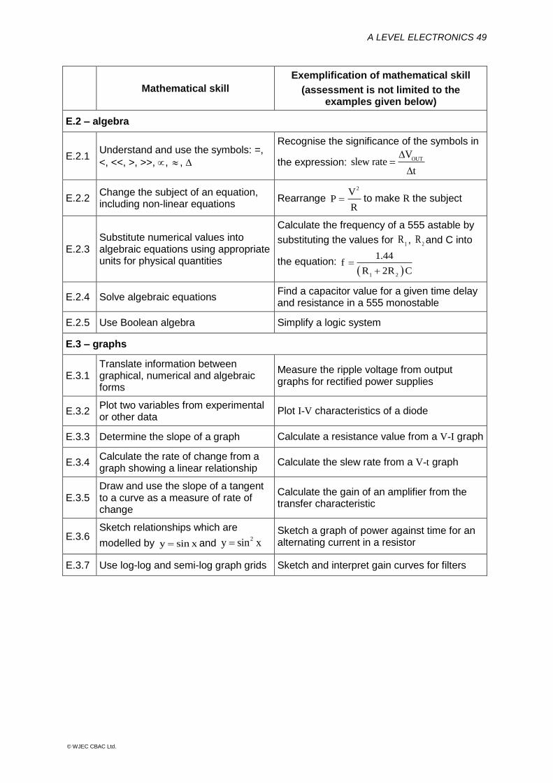
© WJEC CBAC Ltd.
Mathematical skill
Exemplification of mathematical skill
(assessment is not limited to the examples given below)
E.2 – algebra
E.2.1 Understand and use the symbols: =,
<, <<, >, >>, , ,
Recognise the significance of the symbols in
the expression: OUT
Vslew rate
t
E.2.2 Change the subject of an equation, including non-linear equations
Rearrange 2
VP
R to make R the subject
E.2.3 Substitute numerical values into algebraic equations using appropriate units for physical quantities
Calculate the frequency of a 555 astable by
substituting the values for 1R , 2
R and C into
the equation: 1 2
1.44f
R 2R C
E.2.4 Solve algebraic equations Find a capacitor value for a given time delay and resistance in a 555 monostable
E.2.5 Use Boolean algebra Simplify a logic system
E.3 – graphs
E.3.1 Translate information between graphical, numerical and algebraic forms
Measure the ripple voltage from output graphs for rectified power supplies
E.3.2 Plot two variables from experimental or other data
Plot I-V characteristics of a diode
E.3.3 Determine the slope of a graph Calculate a resistance value from a V-I graph
E.3.4 Calculate the rate of change from a graph showing a linear relationship
Calculate the slew rate from a V-t graph
E.3.5 Draw and use the slope of a tangent to a curve as a measure of rate of change
Calculate the gain of an amplifier from the transfer characteristic
E.3.6 Sketch relationships which are
modelled by y sin x and 2
y sin x
Sketch a graph of power against time for an alternating current in a resistor
E.3.7 Use log-log and semi-log graph grids Sketch and interpret gain curves for filters
A LEVEL ELECTRONICS 50
© WJEC CBAC Ltd.
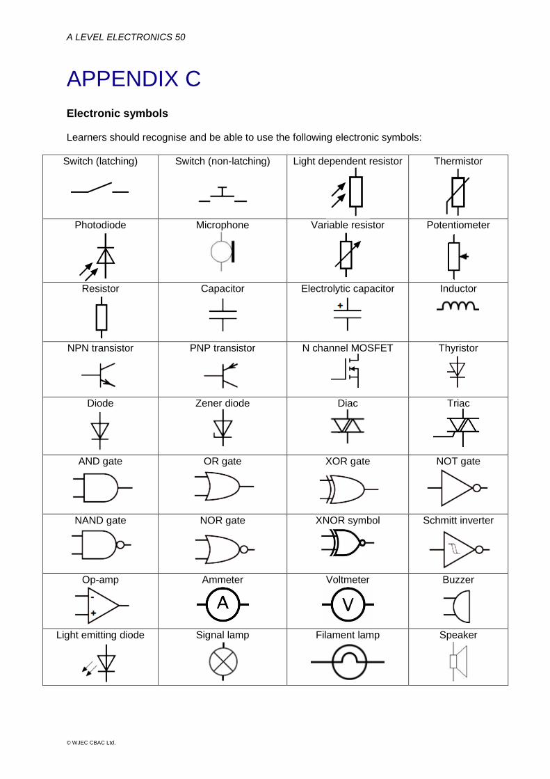
APPENDIX C Electronic symbols Learners should recognise and be able to use the following electronic symbols:
Switch (latching)
Switch (non-latching)
Light dependent resistor
Thermistor
Photodiode
Microphone
Variable resistor
Potentiometer
Resistor
Capacitor
Electrolytic capacitor
Inductor
NPN transistor
PNP transistor
N channel MOSFET
Thyristor
Diode
Zener diode
Diac
Triac
AND gate
OR gate
XOR gate
NOT gate
NAND gate
NOR gate
XNOR symbol
Schmitt inverter
Op-amp
Ammeter
Voltmeter
Buzzer
Light emitting diode
Signal lamp
Filament lamp
Speaker
A LEVEL ELECTRONICS 51
© WJEC CBAC Ltd.
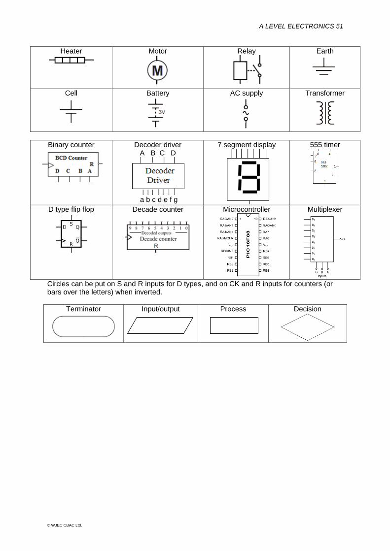
Heater
Motor
Relay
Earth
Cell
Battery
AC supply
Transformer
Binary counter
Decoder driver A B C D
a b c d e f g
7 segment display
555 timer
D type flip flop
Decade counter
Microcontroller
Multiplexer
Circles can be put on S and R inputs for D types, and on CK and R inputs for counters (or bars over the letters) when inverted.
Terminator
Input/output
Process
Decision
A LEVEL ELECTRONICS 52
© WJEC CBAC Ltd.
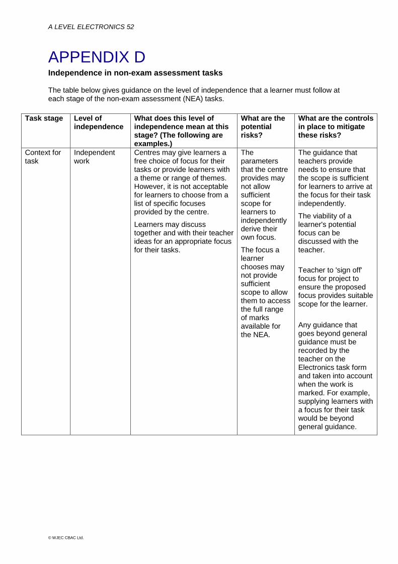
APPENDIX D Independence in non-exam assessment tasks The table below gives guidance on the level of independence that a learner must follow at each stage of the non-exam assessment (NEA) tasks.
Task stage Level of independence
What does this level of independence mean at this stage? (The following are examples.)
What are the potential risks?
What are the controls in place to mitigate these risks?
Context for task
Independent work
Centres may give learners a free choice of focus for their tasks or provide learners with a theme or range of themes. However, it is not acceptable for learners to choose from a list of specific focuses provided by the centre.
Learners may discuss together and with their teacher ideas for an appropriate focus for their tasks.
The parameters that the centre provides may not allow sufficient scope for learners to independently derive their own focus.
The focus a learner chooses may not provide sufficient scope to allow them to access the full range of marks available for the NEA.
The guidance that teachers provide needs to ensure that the scope is sufficient for learners to arrive at the focus for their task independently.
The viability of a learner's potential focus can be discussed with the teacher.
Teacher to 'sign off' focus for project to ensure the proposed focus provides suitable scope for the learner.
Any guidance that goes beyond general guidance must be recorded by the teacher on the Electronics task form and taken into account when the work is marked. For example, supplying learners with a focus for their task would be beyond general guidance.
A LEVEL ELECTRONICS 53
© WJEC CBAC Ltd.
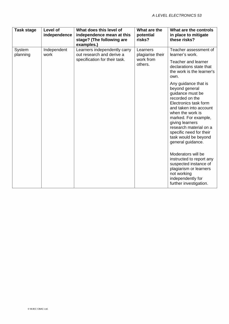
Task stage Level of independence
What does this level of independence mean at this stage? (The following are examples.)
What are the potential risks?
What are the controls in place to mitigate these risks?
System planning
Independent work
Learners independently carry out research and derive a specification for their task.
Learners plagiarise their work from others.
Teacher assessment of learner’s work.
Teacher and learner declarations state that the work is the learner's own.
Any guidance that is beyond general guidance must be recorded on the Electronics task form and taken into account when the work is marked. For example, giving learners research material on a specific need for their task would be beyond general guidance.
Moderators will be instructed to report any suspected instance of plagiarism or learners not working independently for further investigation.
A LEVEL ELECTRONICS 54
© WJEC CBAC Ltd.
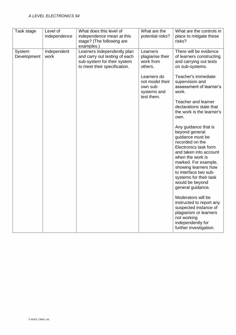
Task stage Level of independence
What does this level of independence mean at this stage? (The following are examples.)
What are the potential risks?
What are the controls in place to mitigate these risks?
System Development
Independent work
Learners independently plan and carry out testing of each sub-system for their system to meet their specification.
Learners plagiarise their work from others. Learners do not model their own sub-systems and test them.
There will be evidence of learners constructing and carrying out tests on sub-systems. Teacher's immediate supervision and assessment of learner’s work. Teacher and learner declarations state that the work is the learner's own. Any guidance that is beyond general guidance must be recorded on the Electronics task form and taken into account when the work is marked. For example, showing learners how to interface two sub-systems for their task would be beyond general guidance. Moderators will be instructed to report any suspected instance of plagiarism or learners not working independently for further investigation.
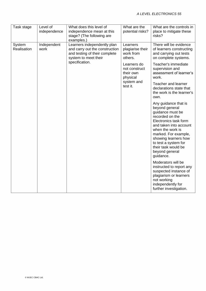
A LEVEL ELECTRONICS 55
© WJEC CBAC Ltd.
Task stage Level of independence
What does this level of independence mean at this stage? (The following are examples.)
What are the potential risks?
What are the controls in place to mitigate these risks?
System Realisation
Independent work
Learners independently plan and carry out the construction and testing of their complete system to meet their specification.
Learners plagiarise their work from others.
Learners do not construct their own physical system and test it.
There will be evidence of learners constructing and carrying out tests on complete systems.
Teacher's immediate supervision and assessment of learner’s work.
Teacher and learner declarations state that the work is the learner's own.
Any guidance that is beyond general guidance must be recorded on the Electronics task form and taken into account when the work is marked. For example, showing learners how to test a system for their task would be beyond general guidance.
Moderators will be instructed to report any suspected instance of plagiarism or learners not working independently for further investigation.

A LEVEL ELECTRONICS 56
© WJEC CBAC Ltd.
Task stage Level of independence
What does this level of independence mean at this stage? (The following are examples.)
What are the potential risks?
What are the controls in place to mitigate these risks?
Evaluation Independent work
Learners independently evaluate the performance of their complete system and suggest improvements.
Learners plagiarise their work from others.
Teacher assessment of learner’s work.
Teacher and learner declarations state that the work is the learner's own.
Any guidance that is beyond general guidance must be recorded on the Electronics task form and taken into account when the work is marked. For example, supplying learners with points to discuss in the evaluation for their task would be beyond general guidance.
Moderators will be instructed to report any suspected instance of plagiarism or learners not working independently for further investigation.
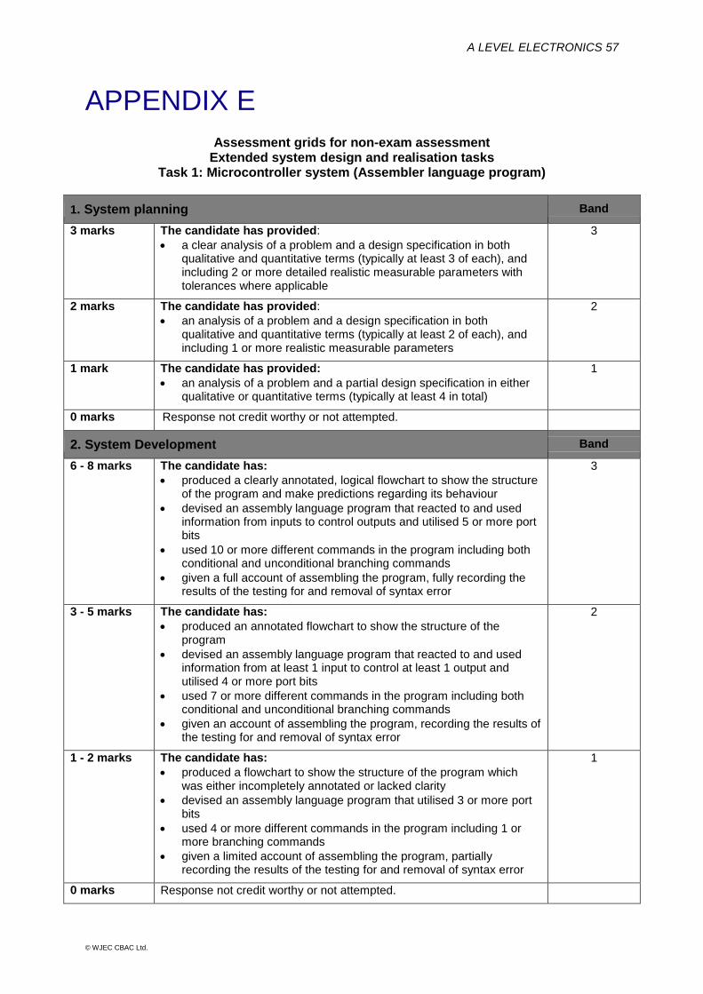
A LEVEL ELECTRONICS 57
© WJEC CBAC Ltd.
APPENDIX E
Assessment grids for non-exam assessment Extended system design and realisation tasks
Task 1: Microcontroller system (Assembler language program)
1. System planning Band
3 marks The candidate has provided:
a clear analysis of a problem and a design specification in both qualitative and quantitative terms (typically at least 3 of each), and including 2 or more detailed realistic measurable parameters with tolerances where applicable
3
2 marks The candidate has provided:
an analysis of a problem and a design specification in both qualitative and quantitative terms (typically at least 2 of each), and including 1 or more realistic measurable parameters
2
1 mark The candidate has provided:
an analysis of a problem and a partial design specification in either qualitative or quantitative terms (typically at least 4 in total)
1
0 marks Response not credit worthy or not attempted.
2. System Development Band
6 - 8 marks The candidate has:
produced a clearly annotated, logical flowchart to show the structure of the program and make predictions regarding its behaviour
devised an assembly language program that reacted to and used information from inputs to control outputs and utilised 5 or more port bits
used 10 or more different commands in the program including both conditional and unconditional branching commands
given a full account of assembling the program, fully recording the results of the testing for and removal of syntax error
3
3 - 5 marks The candidate has:
produced an annotated flowchart to show the structure of the program
devised an assembly language program that reacted to and used information from at least 1 input to control at least 1 output and utilised 4 or more port bits
used 7 or more different commands in the program including both conditional and unconditional branching commands
given an account of assembling the program, recording the results of the testing for and removal of syntax error
2
1 - 2 marks The candidate has:
produced a flowchart to show the structure of the program which was either incompletely annotated or lacked clarity
devised an assembly language program that utilised 3 or more port bits
used 4 or more different commands in the program including 1 or more branching commands
given a limited account of assembling the program, partially recording the results of the testing for and removal of syntax error
1
0 marks Response not credit worthy or not attempted.
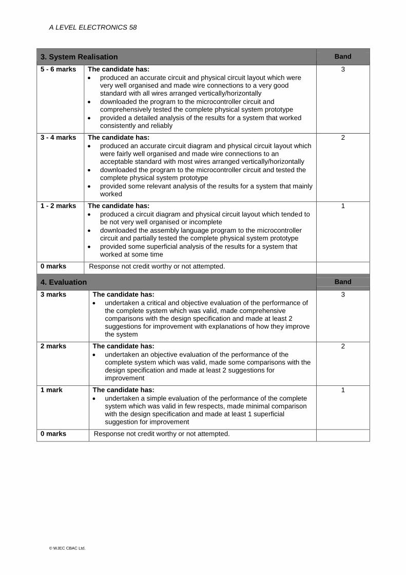
A LEVEL ELECTRONICS 58
© WJEC CBAC Ltd.
3. System Realisation Band
5 - 6 marks The candidate has:
produced an accurate circuit and physical circuit layout which were very well organised and made wire connections to a very good standard with all wires arranged vertically/horizontally
downloaded the program to the microcontroller circuit and comprehensively tested the complete physical system prototype
provided a detailed analysis of the results for a system that worked consistently and reliably
3
3 - 4 marks The candidate has:
produced an accurate circuit diagram and physical circuit layout which were fairly well organised and made wire connections to an acceptable standard with most wires arranged vertically/horizontally
downloaded the program to the microcontroller circuit and tested the complete physical system prototype
provided some relevant analysis of the results for a system that mainly worked
2
1 - 2 marks The candidate has:
produced a circuit diagram and physical circuit layout which tended to be not very well organised or incomplete
downloaded the assembly language program to the microcontroller circuit and partially tested the complete physical system prototype
provided some superficial analysis of the results for a system that worked at some time
1
0 marks Response not credit worthy or not attempted.
4. Evaluation Band
3 marks The candidate has:
undertaken a critical and objective evaluation of the performance of the complete system which was valid, made comprehensive comparisons with the design specification and made at least 2 suggestions for improvement with explanations of how they improve the system
3
2 marks The candidate has:
undertaken an objective evaluation of the performance of the complete system which was valid, made some comparisons with the design specification and made at least 2 suggestions for improvement
2
1 mark The candidate has:
undertaken a simple evaluation of the performance of the complete system which was valid in few respects, made minimal comparison with the design specification and made at least 1 superficial suggestion for improvement
1
0 marks Response not credit worthy or not attempted.
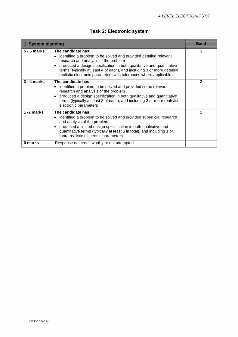
A LEVEL ELECTRONICS 59
© WJEC CBAC Ltd.
Task 2: Electronic system
1. System planning Band
5 - 6 marks The candidate has:
identified a problem to be solved and provided detailed relevant research and analysis of the problem
produced a design specification in both qualitative and quantitative terms (typically at least 4 of each), and including 3 or more detailed realistic electronic parameters with tolerances where applicable
3
3 - 4 marks The candidate has:
identified a problem to be solved and provided some relevant research and analysis of the problem
produced a design specification in both qualitative and quantitative terms (typically at least 3 of each), and including 2 or more realistic electronic parameters
2
1 -2 marks The candidate has:
identified a problem to be solved and provided superficial research and analysis of the problem
produced a limited design specification in both qualitative and quantitative terms (typically at least 5 in total), and including 1 or more realistic electronic parameters
1
0 marks Response not credit worthy or not attempted.
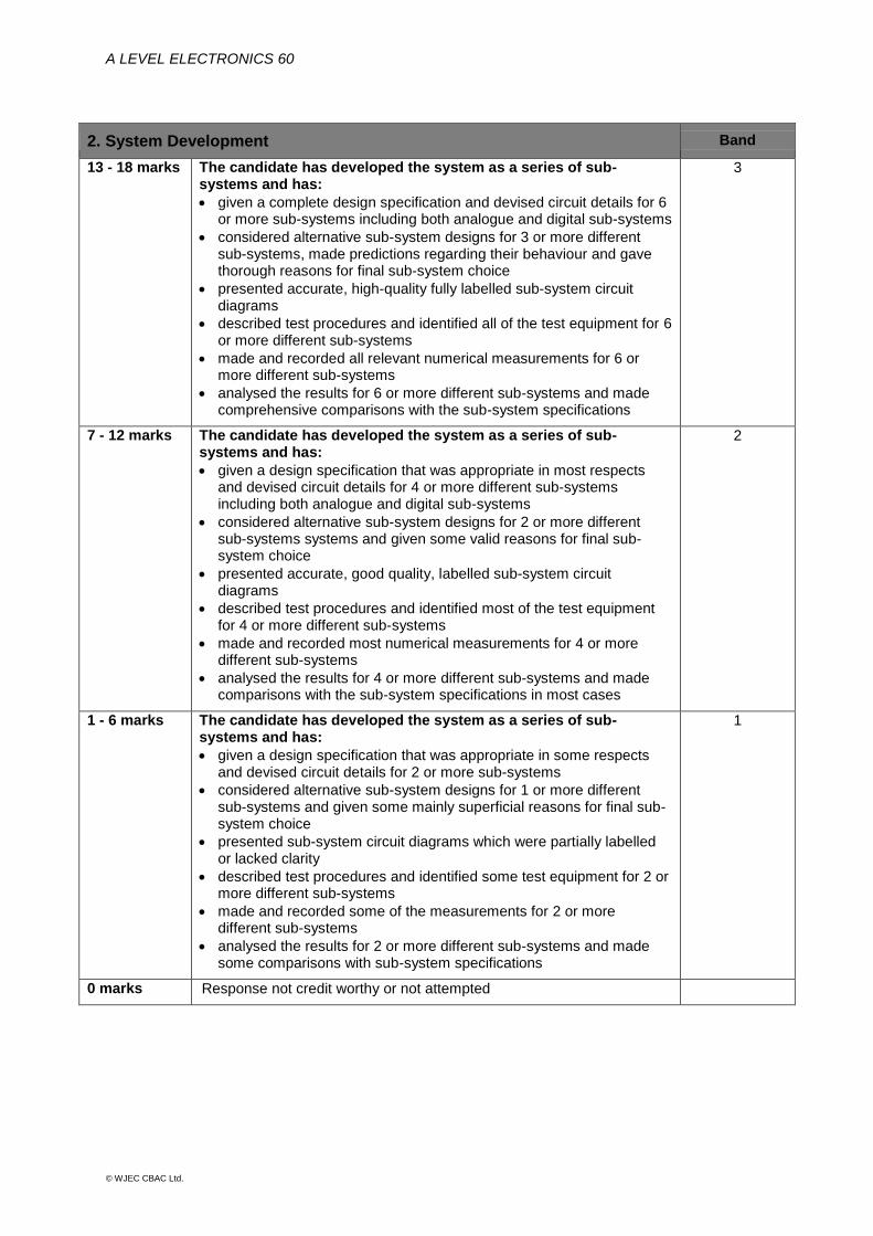
A LEVEL ELECTRONICS 60
© WJEC CBAC Ltd.
2. System Development Band
13 - 18 marks The candidate has developed the system as a series of sub-systems and has:
given a complete design specification and devised circuit details for 6 or more sub-systems including both analogue and digital sub-systems
considered alternative sub-system designs for 3 or more different sub-systems, made predictions regarding their behaviour and gave thorough reasons for final sub-system choice
presented accurate, high-quality fully labelled sub-system circuit diagrams
described test procedures and identified all of the test equipment for 6 or more different sub-systems
made and recorded all relevant numerical measurements for 6 or more different sub-systems
analysed the results for 6 or more different sub-systems and made comprehensive comparisons with the sub-system specifications
3
7 - 12 marks The candidate has developed the system as a series of sub-systems and has:
given a design specification that was appropriate in most respects and devised circuit details for 4 or more different sub-systems including both analogue and digital sub-systems
considered alternative sub-system designs for 2 or more different sub-systems systems and given some valid reasons for final sub-system choice
presented accurate, good quality, labelled sub-system circuit diagrams
described test procedures and identified most of the test equipment for 4 or more different sub-systems
made and recorded most numerical measurements for 4 or more different sub-systems
analysed the results for 4 or more different sub-systems and made comparisons with the sub-system specifications in most cases
2
1 - 6 marks The candidate has developed the system as a series of sub-systems and has:
given a design specification that was appropriate in some respects and devised circuit details for 2 or more sub-systems
considered alternative sub-system designs for 1 or more different sub-systems and given some mainly superficial reasons for final sub-system choice
presented sub-system circuit diagrams which were partially labelled or lacked clarity
described test procedures and identified some test equipment for 2 or more different sub-systems
made and recorded some of the measurements for 2 or more different sub-systems
analysed the results for 2 or more different sub-systems and made some comparisons with sub-system specifications
1
0 marks Response not credit worthy or not attempted
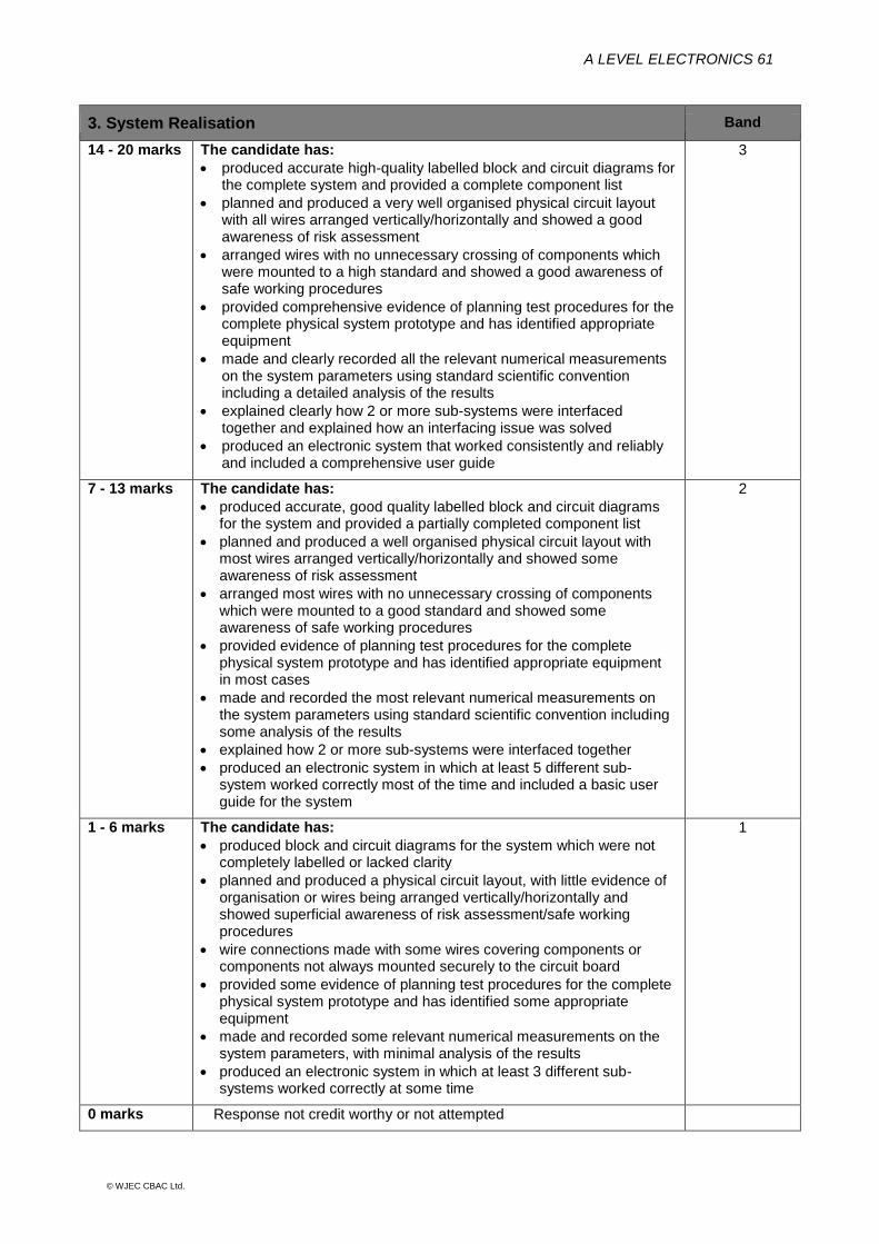
A LEVEL ELECTRONICS 61
© WJEC CBAC Ltd.
3. System Realisation Band
14 - 20 marks The candidate has:
produced accurate high-quality labelled block and circuit diagrams for the complete system and provided a complete component list
planned and produced a very well organised physical circuit layout with all wires arranged vertically/horizontally and showed a good awareness of risk assessment
arranged wires with no unnecessary crossing of components which were mounted to a high standard and showed a good awareness of safe working procedures
provided comprehensive evidence of planning test procedures for the complete physical system prototype and has identified appropriate equipment
made and clearly recorded all the relevant numerical measurements on the system parameters using standard scientific convention including a detailed analysis of the results
explained clearly how 2 or more sub-systems were interfaced together and explained how an interfacing issue was solved
produced an electronic system that worked consistently and reliably and included a comprehensive user guide
3
7 - 13 marks The candidate has:
produced accurate, good quality labelled block and circuit diagrams for the system and provided a partially completed component list
planned and produced a well organised physical circuit layout with most wires arranged vertically/horizontally and showed some awareness of risk assessment
arranged most wires with no unnecessary crossing of components which were mounted to a good standard and showed some awareness of safe working procedures
provided evidence of planning test procedures for the complete physical system prototype and has identified appropriate equipment in most cases
made and recorded the most relevant numerical measurements on the system parameters using standard scientific convention including some analysis of the results
explained how 2 or more sub-systems were interfaced together
produced an electronic system in which at least 5 different sub-system worked correctly most of the time and included a basic user guide for the system
2
1 - 6 marks The candidate has:
produced block and circuit diagrams for the system which were not completely labelled or lacked clarity
planned and produced a physical circuit layout, with little evidence of organisation or wires being arranged vertically/horizontally and showed superficial awareness of risk assessment/safe working procedures
wire connections made with some wires covering components or components not always mounted securely to the circuit board
provided some evidence of planning test procedures for the complete physical system prototype and has identified some appropriate equipment
made and recorded some relevant numerical measurements on the system parameters, with minimal analysis of the results
produced an electronic system in which at least 3 different sub-systems worked correctly at some time
1
0 marks Response not credit worthy or not attempted
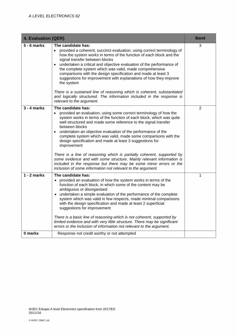
A LEVEL ELECTRONICS 62
© WJEC CBAC Ltd.
4. Evaluation (QER) Band
5 - 6 marks The candidate has:
provided a coherent, succinct evaluation, using correct terminology of how the system works in terms of the function of each block and the signal transfer between blocks
undertaken a critical and objective evaluation of the performance of the complete system which was valid, made comprehensive comparisons with the design specification and made at least 3 suggestions for improvement with explanations of how they improve the system
There is a sustained line of reasoning which is coherent, substantiated and logically structured. The information included in the response is relevant to the argument.
3
3 - 4 marks The candidate has:
provided an evaluation, using some correct terminology of how the system works in terms of the function of each block, which was quite well structured and made some reference to the signal transfer between blocks
undertaken an objective evaluation of the performance of the complete system which was valid, made some comparisons with the design specification and made at least 3 suggestions for improvement
There is a line of reasoning which is partially coherent, supported by some evidence and with some structure. Mainly relevant information is included in the response but there may be some minor errors or the inclusion of some information not relevant to the argument.
2
1 - 2 marks The candidate has:
provided an evaluation of how the system works in terms of the function of each block, in which some of the content may be ambiguous or disorganised
undertaken a simple evaluation of the performance of the complete system which was valid in few respects, made minimal comparisons with the design specification and made at least 2 superficial suggestions for improvement
There is a basic line of reasoning which is not coherent, supported by limited evidence and with very little structure. There may be significant errors or the inclusion of information not relevant to the argument.
1
0 marks Response not credit worthy or not attempted
WJEC Eduqas A level Electronics specification from 2017/ED 25/11/16