wmx-ji19000 intel baytrail j1900 user manual rev. 02, oct ... · wmx-ji19000 intel® baytrail j1900...
TRANSCRIPT

WMX-JI19000 Intel® BayTrail J1900 User Manual Rev. 02, Oct. 2014

2
Contents
Chapter 1 Product Information ................................................................................ 4 1.1 Block Diagram ............................................................................................. 4 1.2 Features ....................................................................................................... 5 1.3 PCB Layout ................................................................................................. .8 1.4 Jumper Setting .......................................................................................... 10 1.5 Connector Function List .......................................................................... .13 1.6 Connector Definitions .............................................................................. .15
1.6 I/O Ports Power Output (max.) ………………………………………………..32 Chapter 2 BIOS Setup ............................................................................................ 34
2.1 Main Menu .................................................................................................. 34 2.2 Advanced Menu ......................................................................................... 35 2.3 ACPI Settings ............................................................................................. 37 2.4 Super IO Configuration ............................................................................. 38 2.5 Serial Port 1 Configuration ...................................................................... .39 2.6 Serial Port 2 Configuration ....................................................................... 40 2.7 Serial Port 3 Configuration ...................................................................... .41 2.8 Serial Port 4 Configuration ...................................................................... .42 2.9 Serial Port 5 Configuration ...................................................................... .43 2.10 Serial Port 6 Configuration .................................................................... .44 2.11 PC Health Status ..................................................................................... .45 2.12 Smart Fan Mode Configuration ............................................................. .46 2.13 CPU Configuratio .................................................................................... .47 2.14 IDE Configuration ................................................................................... .48 2.15 Network Stack Configuration ................................................................ .50 2.16 Compatibility Support Module Configuration ...................................... .51 2.17 USB Configuration ................................................................................. .53 2.18 Chipset .................................................................................................... .55 2.19 Memory Information ............................................................................... .56 2.20 Intel IGD Configuration .......................................................................... .57 2.21 USB Configuration .................................................................................. 60 2.22 XHCI Mode ............................................................................................... 61 2.23 PCI Express Configuration .................................................................... .62
2.24 Passeord Configuration.……………………………………………………...63 2.25 Boot Configuration ................................................................................. .64 2.25 Save Changes and Exit………………………………………………………..65
Chapter 3 Drivers Installation ................................................................................ 68

3
3.1 Intel Chipset Device Software .................................................................. 68 3.2 Intel Graphic Media Accelerator Driver .................................................... 70 3.3 LAN Driver .................................................................................................. 74 3.4 Audio Driver. .............................................................................................. 77
3.5 TXE Driver………………………………………………………………………...77
3.6 USB Driver ……………………………………………………………………….80 Appendix A: Watchdog Timer ................................................................................ 82 Appendix B: GPIO .................................................................................................. 85

4
Chapter 1 Product Information This chapter introduces the product features, jumper and connector information. 1.1 Block Diagram
The block diagram below shows the architecture and main components of the
WMX-J19000. The key component on the board is the Intel® Celeron™ J1900
(Bay Trail) platform controller SoC.

5
1.2 Features
System Processor/Chipsets
Processor
Intel® Celeron™ Processor J1900 Product
(Bay Trail Platform)
FCBGA1170 Package 25.0mm x 27.0mm
BIOS AMI® BIOS, 64Mbit SPI Low Power Flash ROM
Memory
Technology
Celeron™ Processors DDR3L 1333 MT/s
DDR3L DRAM Device Technology — Standard 1Gb/2Gb/4Gb technologies and addressing.
— Read latency 5, 6, 7, 8, 9, 10, 11.
— Write latency 5, 6, 7, 8.
Max. Capacity Up to 8GB DDR3L DRAM
Socket 1 x DDR3L SO-DIMM (+1.35V)
Display
Chipset Intel® 7th generation (Gen 7) graphics and media
encode/decode engine
VRAM Shared system memory up to 512MB (max.)
LVDS 24bit, Dual Channel
max resolution up to 1920 x 1200 @ 60Hz
VGA Analog Display:
max resolution up to 2560 x 1600 @ 60Hz
DVI-D Digital Display:
max resolution up to 1920 x 1200 @ 60Hz
Any 2
Displays
(1) LVDS+DVI-D
(2) LVDS+VGA
(3) DVI-D+VGA
Ethernet
Interface PCIe x1 Gigabit LAN 10/100/1000 Mb/s
Controller LAN1: Intel® Ethernet Controller I210
LAN2: Intel® Ethernet Controller I210
Audio Interface Intel® High Definition Audio
Controller Realtek® ALC662-VD0 HD Audio Codec

6
Expansion Slot
PCIe x1 1
MINI-PCIE 1 (Full size with mSATA support by jumper
selector and SIM Card Board)
SATA
Max. Data
Transfer RateSATA II:3.0Gb/s
Port
SATA II x1,
mSATA x1 (Share MINI-PCIE slot)
Integrated AHCI controller
Onboard Conn. and Pin-Header
ATX 12V 1 (2x2 pin)
COM 4 (RS-232)
CPU Fan 1 (4pin.)
DIO 4 in/4 out (sink 6A x2)
FP_HDA 1 (Line-in2/Mic-in2)
FRONT 1 (Power/HDD/Suspend-LED/PwrBTN/RstBTN)
LVDS 1 (with Inverter power pin header)
Micro SD 1 (MicroSD/T-Flash, support SDHC)
PS/2 1 (PS/2 Keyboard and Mouse)
SATA II 1
SMBus 1
SYS Fan 1 (3pin.)
USB 2.0 2 (x4 ports)
WEBCAM 1 (USB 2.0 Interface)
Rear I/O
Audio 3 (Line-in, Line-out, Mic-in)
COM
2 (1xRS232,1xRS232/RS422/RS485); all support
12V/5V/RI# jumper selector.
※1. COM2 RS-422/485 support Half/Full Duplex.
※2. COM2 RS-232 Slew Rate 1Mbps (max.).
※3. COM2 RS-422/485 Slew Rate 20Mbps (max.).
DC-Jack 1 (+12Vdc ~ +24Vdc)

7
Rear I/O
DVI-D 1
LAN 2 x RJ45
USB 2.0 3
USB 3.0 1
VGA 1
Power DC-Jack 1 (+12Vdc ~ +24Vdc)
ATX 4P 1 (only +12Vdc)
Watchdog Timer Interval Programmable 1~255 sec./min.
Output System reset
Energy EuP/ErP EuP/ErP 2013 Ready
Power off mode (G3) < 0.5W
Environment
Operating
Temp. 0°C ~ +60°C (standard)
Storage
Temp.
-20°C ~ +80°C and 60°C @ 95% RH
non-condensing
Relative
Humidity 0%~ 95% (non-condensing)
Form Factor Dimension
(L*W)
Mini-ITX
170mm x 170mm (6.69” x 6.69”)
*** WMX-J19000 base unit will be RoHS / Halogen free compliant from LP/MP phase.
*** The content is subjected to change without notice.
Intel® Bay Trail
DVI‐D / VGA / LVDS 24bit
FanlessMini‐ITX
Wide
+12~24Vdc
Dual Intel®
GbE LANUSB2.0 x7
USB3.0 x1
RS‐232 x5
x1RS‐422RS‐485
SATA x1
mSATA x1 MicroSDx1
Dual Display
ErP/EuP
READY
DIO x8Watchdog

8
1.3 PCB Layout
WMX‐J19000 Top View
CPUFAN
SPI
JPLVDS LVDS JLVDS INV SATAPWR SATA
JTRTCJCMOS
DIO KB_MS SYSFAN
JPCOM3
JPCOM4
JPCOM5
JPCOM6
FRONT
BZ
COM3
COM4
JMINI-PCIE
JPWR
COM5
COM6
BAT1
CHA-DIMM
CPU
PWR2
PWR1DVI-D_VGA COM1_COM2
JPCOM2
JPCOM1
JCOM2
USB2_LAN2 USB1_LAN1 AUDIOFP_HDA
PCIE
SMB
WEBCAM
LPCUSB3 USB4
SIMBD
MINI-PCIE

9
WMX‐J19000 Bottom View MICRO-SD
BARCODR LABEL
WMX‐J19000 Rear I/O View
PWR1 DVI‐D_VGA COM1_COM2 USB2_LAN2 USB1_LAN1 AUDIO

10
123
123
123
123
123
123
123
123
1.4 Jumper Setting
JCMOS: CMOS Clear Selection
Pin No. 1-2 2-3
Function Normal Operation (Default) Clear CMOS Contents
Jumper
Setting
JTRTC: RTC Register Clear Selection
Pin No. 1-2 2-3
Function Normal Operation (Default) Clear RTC Register Contents
Jumper
Setting
JCOM2: COM2 RS-232/422/485 Slew Rate Selection
Pin No. 1-2 2-3
Function RS-232 Slew Rate 250Kbps
RS-422/RS-485 Slew Rate 250Kbps
(Default)
RS-232 Slew Rate 1Mbps
RS-422/RS-485 Slew Rate 20Mbps
Jumper
Setting
JMINI-PCIE: Mini-PCIe / mSATA Function (by manual setting)
Pin No. 1-2 2-3
Function MINI-PCIE = PCIe signal
Mini-PCIe work (Default)
MINI-PCIE = mSATA signal
mSATA work
Jumper
Setting

11
JLVDS: LCD Panel Type Selection
Jumper Setting LCD Panel Type Jumper Setting LCD Panel Type
800 x 600
18bit 1-2, 3-4, 5-6, 7-8 (0000) - (Default)
1024 x 768
18bit 3-4, 5-6, 7-8
(1000)
1024 x 768
24bit 1-2, 5-6, 7-8
(0100)
1280 x 768
18bit 5-6, 7-8 (1100)
1280 x 800
18bit 1-2, 3-4, 7-8
(0010)
1280 x 960
18bit 3-4, 7-8 (1010)
1280 x 1024
24bit 1-2, 7-8 (0110)
1366 x 768
18bit 7-8
(1110)
1366 x 768
24bit 1-2, 3-4, 5-6
(0001)
1440 x 900
24bit 3-4, 5-6 (1001)
1440 x 1050
24bit 1-2, 5-6 (0101)
1600 x 900
24bit 5-6
(1101)
1680 x 1050
24bit 1-2, 3-4 (0011)
1600 x 1200
24bit 3-4
(1011)
1920 x 1080
24bit 1-2
(0111)
1920 x 1200
24bit NC
(1111)
Note: Open = High (1), Close = Low (0).

12
1 3 5
2 4 6
1 3 5
2 4 6
1 3 5
2 4 6
1 3 5
2 4 6
1 3 5
2 4 6
1 3 5
2 4 6
1 3 5
2 4 6
1 3 5
2 4 6
1 3 5
2 4 6
123
123
JPCOM1~JPCOM2: COM1~COM2 pin.9 (5V/12V/RI#) Selection
Pin No. 1-2 3-4 5-6
Function +5VModem Ring In
(Default) +12V
Jumper
Setting
JPCOM3~JPCOM6: COM3~COM6 pin.8 (5V/12V/RI#) Selection
Pin No. 1-2 3-4 5-6
Function +5VModem Ring In
(Default) +12V
Jumper
Setting
JPLVDS: LCD Panel Power (3.3V/5V/12V) Selection
Pin No. 1-3 3-4 3-5
Function LCD Power +3.3V
(Default) LCD Power +12V LCD Power +5V
Jumper
Setting
JPWR: AT/ATX Mode Selection
Pin No. 1-2 2-3
Function AT Mode ATX Mode (Default)
Jumper
Setting

13
1.5 Connector Function List
Rear I/O Port List
Connector Function Note
AUDIO Line-in / Line-out / Mic-in connector
COM1_COM2 COM1, RS-232 serial port (DB9) connector
COM2, RS-232/422/485 serial port (DB9) connector
DVI-D_VGA DVI-D, DVI digital connector
VGA, VGA (DB15) connector
PWR1 DC-Jack 4pin connector (+12Vdc ~ +24Vdc)
USB1_LAN1 USB1, USB3.0 x1 / USB2.0 x1 conenctor
LAN1, RJ45 (LAN) conenctor
USB2_LAN2 USB2, USB2.0 x2 conenctor
LAN2, RJ45 (LAN) conenctor
On Board Expansion Slot List
Connector Function Note
BAT1 CMOS battery (CR2032) slot
CHA-DIMM DDR3L SO-DIMM slot
MINI-PCIE miniPCIe Express (full-size) or mSATA slot (share)
PCIE PCI Express x1 slot
MICRO-SD Micro SD / T-Flash slot
On Board I/O Connector List (1/2)
Connector Function Note
COM3, COM4,
COM5, COM6 RS-232 serial ports with box-header
CPUFAN CPU FAN 4-pin connector
DIO Digital I/O with pin-header
FP_HDA Front Panel audio with pin-header
FRONT Front Panel with pin-header
INV LCD inverter with box-header

14
On Board I/O Connector List (2/2) Connector Function Note
KB_MS PS/2 keyboard and mouse with box-header
LVDS LCD panel LVDS 18/24bit connector
PWR2 ATX +12V 2x2 pin (4-pole) connector
SATA SATA 2.0 port connector
SATAPWR SATA power box-header (+5V and +12V)
SMB SMBus with pin-header
SYSFAN System FAN 3-pin connector
USB3, USB4 USB2.0 with pin-header
WEBCAM Webcam with box-header
LPC Reserved for debug with pin-header
SPI Reserved for debug with pin-header

15
1.6 Connector Definitions
The following sections provide pin definitions and detailed description of all on-board
connectors. The connector definitions follow the following notation:
Column Name
Description
Pin Shows the pin-numbers in the connector. The graphical layout of the
connector definition tables is made similar to the physical connectors.
Type Al Analogue Input.
AO Analogue Output. I Input, TTL compatible if nothing else stated.
IO Input / Output TTL compatible if nothing else stated.
IOT Bi-directional tri-state IO pin.
IS Schmitt-trigger input, TTL compatible.
IOC Input/open-collector Output, TTL compatible.
IOD Input / Output, CMOS level Schmitt-triggered (open drain output).
NC Pin not connected.
O Output, TTL compatible.
OC Output, open-collector or open-drain, TTL compatible.
OT Output with tri-state capability, TTL compatible.
DIFF Differential Signal.
PWR Power supply or ground reference pins.
IOH Typical current in mA flowing out of an output pin through a
grounded load, while the output voltage is > 2.4 V DC (if nothing
else stated).
IOL Typical current in mA flowing into an output pin from a VCC
connected load, while the output voltage is < 0.4 V DC (if nothing
else stated).
Signal The mnemonic name of the signal at the current pin. The notation “XX#”
states that the signal “XX” is active low. Note Special remarks concerning the signal.
※ The abbreviation TBD is used for specifications which are not available yet or which are
not sufficiently specified by the component vendors.

16
Rear I/O Port Pin Define
AUDIO: Line-in / Line-out / MIC-in Connectors
AUDIO Pin Type Signal Note
32 AI Line-in (Left) Phone Jack
LINE-IN
(Blue)
33 PWR Ground
34 AI Line-in (Detect)
35 AI Line-in (Right)
22 AI Line-out (Left) Phone Jack
LINE-OUT
(Green)
23 PWR Ground
24 AI Line-out (Detect)
25 AI Line-out (Right)
1 PWR Audio shield ground Phone Jack
MIC-IN
(Pink)
2 AI Mic-in (Left)
3 PWR Ground
4 AI Mic-in (Detect)
5 AI Mic-in (Right)
COM1_COM2: RS-232/422/485 Serial Port (DB9) Connectors (1/2)
COM1_COM2 Pin TypeSignal RS‐232 | RS‐422 | RS485
Note
10 I Data Carrier Detect (DCD) |TX D-|DATA‐ COM2
(UP)
RS-232
RS-422
RS-485 Pin.18 by
jumper select
11 I Received Data (RXD) |TX D+|DATA+
12 O Transmitted Data (TXD) |RX D+
13 O Data Terminal Ready (DTR)|RX D-
14 PWR Ground
15 I Data Set Ready (DSR)
16 O Request To Send (RTS)
17 I Clear To Send (CTS)
18 I/PWR Ring Indicator (RI#) / +5V / +12V
Note 1: COM1 port pin.9 and COM2 port pin.18 function by jumper select RI# / +5V / +12V.
Note 2: COM1 port pin.9 and COM2 port pin.18 power supply maximum +5V/1.0A or +12V/1.0A

17
COM1_COM2: RS-232/422/485 Serial Port (DB9) Connectors (2/2)
COM1_COM2 Pin Type Signal Note
1 I Data Carrier Detect (DCD)
COM1
(DOWN)
RS-232 Pin.9 by jumper select
2 I Received Data (RXD)
3 O Transmitted Data (TXD)
4 O Data Terminal Ready (DTR)
5 PWR Ground
6 I Data Set Ready (DSR)
7 O Request To Send (RTS)
8 I Clear To Send (CTS)
9 I/PWR Ring Indicator (RI#) / +5V / +12V Note 1: COM1 port pin.9 and COM2 port pin.18 function by jumper select RI# / +5V / +12V.
Note 2: COM1 port pin.9 and COM2 port pin.18 power supply maximum +5V/1.0A or +12V/1.0A
DVI-D_VGA: DVI digital / VGA (DB15) Connectors (1/2)
DVI-D_VGA Pin Type Signal Note
R1 AO VGA Red colour values
VGA
(UP)
R2 AO VGA Green colour values
R3 AO VGA Blue colour values
R4 NC Not connected
R5 PWR Ground
R6 PWR GroundR7 PWR GroundR8 PWR GroundR9 PWR VGA power +5V
R10 PWR Ground
R11 NC Not connected
R12 IO VGA DDC data
R13 O VGA Horizontal synchronization
R14 O VGA Vertical synchronization
R15 IO VGA DDC clock
1 DIFF DVI TMDS DATA2-
DVI-D
(DOWN)
2 DIFF DVI TMDS DATA2+3 PWR DVI TMDS DATA2/4 shield ground
4 NC Not connected
5 NC Not connected
6 IO DVI DDC clock
7 IO DVI DDC data
8 NC Not connected
9 DIFF DVI TMDS DATA1-
10 DIFF DVI TMDS DATA1+
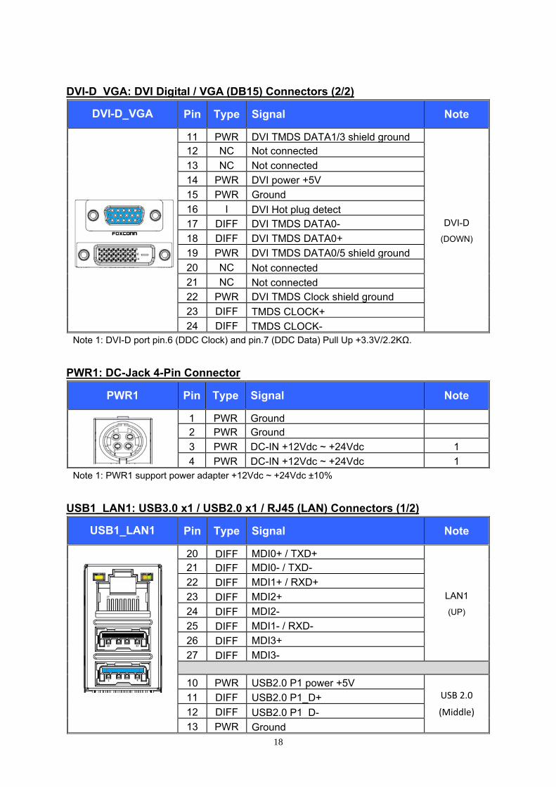
18
DVI-D_VGA: DVI Digital / VGA (DB15) Connectors (2/2)
DVI-D_VGA Pin Type Signal Note
11 PWR DVI TMDS DATA1/3 shield ground
DVI-D
(DOWN)
12 NC Not connected
13 NC Not connected
14 PWR DVI power +5V
15 PWR Ground
16 I DVI Hot plug detect17 DIFF DVI TMDS DATA0-
18 DIFF DVI TMDS DATA0+
19 PWR DVI TMDS DATA0/5 shield ground
20 NC Not connected21 NC Not connected22 PWR DVI TMDS Clock shield ground
23 DIFF TMDS CLOCK+24 DIFF TMDS CLOCK-
Note 1: DVI-D port pin.6 (DDC Clock) and pin.7 (DDC Data) Pull Up +3.3V/2.2KΩ.
PWR1: DC-Jack 4-Pin Connector
PWR1 Pin Type Signal Note
1 PWR Ground 2 PWR Ground
3 PWR DC-IN +12Vdc ~ +24Vdc 1
4 PWR DC-IN +12Vdc ~ +24Vdc 1 Note 1: PWR1 support power adapter +12Vdc ~ +24Vdc ±10%
USB1_LAN1: USB3.0 x1 / USB2.0 x1 / RJ45 (LAN) Connectors (1/2)
USB1_LAN1 Pin Type Signal Note
20 DIFF MDI0+ / TXD+
LAN1
(UP)
21 DIFF MDI0- / TXD-
22 DIFF MDI1+ / RXD+
23 DIFF MDI2+
24 DIFF MDI2-
25 DIFF MDI1- / RXD-
26 DIFF MDI3+
27 DIFF MDI3-
10 PWR USB2.0 P1 power +5VUSB 2.0
(Middle)
11 DIFF USB2.0 P1_D+
12 DIFF USB2.0 P1_D-13 PWR Ground

19
USB1_LAN1: USB3.0 x1 / USB2.0 x1 / RJ45 (LAN) Connectors (2/2)
USB1_LAN1 Pin Type Signal Note
1 PWR USB3.0 P0 power +5V
USB 3.0
(DOWN)
(Blue)
2 DIFF USB2.0 P0_D+
3 DIFF USB2.0 P0_D-
4 PWR Ground
5 DIFF USB3.0 P0_RX-
6 DIFF USB3.0 P0_RX+
7 PWR Ground
8 DIFF USB3.0 P0_TX-
9 DIFF USB3.0 P0_TX+ Note 1: USB 2.0 Port power supply maximum +5V/0.5A
Note 2: USB 3.0 Port power supply maximum +5V/0.9A
USB2_LAN2: USB2.0 x2 / RJ45 (LAN) Connectors
USB2_LAN2 Pin Type Signal Note
L2 DIFF MDI0+ / TXD+
LAN2
(UP)
L3 DIFF MDI0- / TXD-
L4 DIFF MDI1+ / RXD+
L5 DIFF MDI2+
L6 DIFF MDI2-
L7 DIFF MDI1- / RXD-
L8 DIFF MDI3+
L9 DIFF MDI3-
U5 PWR USB2.0 P3 power +5V
USB 2.0
(MIDDLE)
U6 DIFF USB2.0 P3_D+
U7 DIFF USB2.0 P3_D-
U8 PWR Ground
U1 PWR USB2.0 P2 power +5V
USB 2.0
(DOWN)
U2 DIFF USB2.0 P2_D+
U3 DIFF USB2.0 P2_D-
U4 PWR Ground
Note 1: USB 2.0 ports power supply maximum +5V/0.5A
20
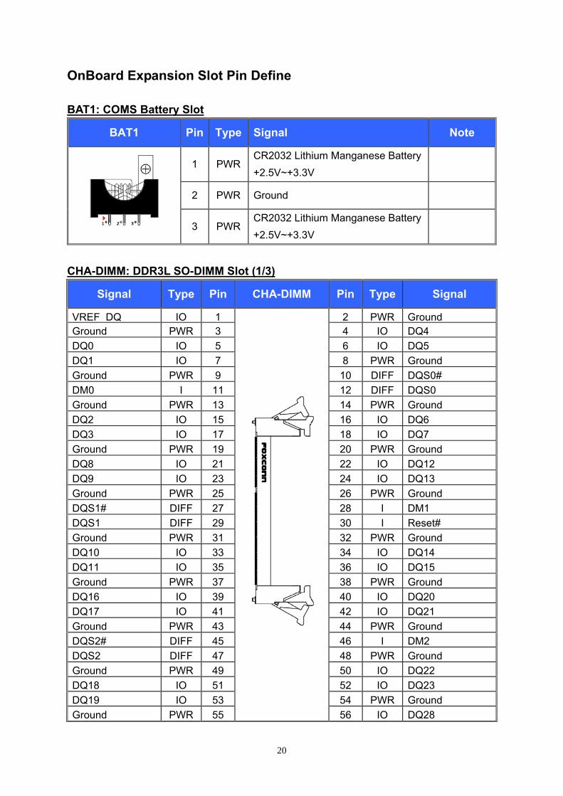
OnBoard Expansion Slot Pin Define BAT1: COMS Battery Slot
BAT1 Pin Type Signal Note
1 PWR
CR2032 Lithium Manganese Battery
+2.5V~+3.3V
2 PWR Ground
3 PWRCR2032 Lithium Manganese Battery
+2.5V~+3.3V
CHA-DIMM: DDR3L SO-DIMM Slot (1/3)
Signal Type Pin CHA-DIMM Pin Type Signal
VREF_DQ IO 1 2 PWR Ground Ground PWR 3 4 IO DQ4
DQ0 IO 5 6 IO DQ5
DQ1 IO 7 8 PWR Ground
Ground PWR 9 10 DIFF DQS0#
DM0 I 11 12 DIFF DQS0
Ground PWR 13 14 PWR Ground
DQ2 IO 15 16 IO DQ6
DQ3 IO 17 18 IO DQ7
Ground PWR 19 20 PWR Ground
DQ8 IO 21 22 IO DQ12
DQ9 IO 23 24 IO DQ13
Ground PWR 25 26 PWR Ground
DQS1# DIFF 27 28 I DM1
DQS1 DIFF 29 30 I Reset#
Ground PWR 31 32 PWR Ground
DQ10 IO 33 34 IO DQ14
DQ11 IO 35 36 IO DQ15
Ground PWR 37 38 PWR Ground
DQ16 IO 39 40 IO DQ20
DQ17 IO 41 42 IO DQ21
Ground PWR 43 44 PWR Ground
DQS2# DIFF 45 46 I DM2
DQS2 DIFF 47 48 PWR Ground
Ground PWR 49 50 IO DQ22
DQ18 IO 51 52 IO DQ23
DQ19 IO 53 54 PWR Ground
Ground PWR 55 56 IO DQ28

21
CHA-DIMM: DDR3L SO-DIMM Slot (2/3)
Signal Type Pin CHA-DIMM Pin Type Signal
DQ24 IO 57 58 IO DQ29 DQ25 IO 59 60 PWR Ground
Ground PWR 61 62 DIFF DQS3#
DM3 I 63 64 DIFF DQS3
Ground PWR 65 66 PWR Ground
DQ26 IO 67 68 IO DQ30
DQ27 IO 69 70 IO DQ31
Ground PWR 71 72 PWR Ground
KEY KEY
CKE0 I 73 74 I CKE1
VDDQ +1.35V ※1 PWR 75 76 PWR VDDQ +1.35V ※1
Not connected NC 77 78 I A15
BA2 I 79 80 I A14
VDDQ +1.35V ※1 PWR 81 82 PWR VDDQ +1.35V ※1
A12 I 83 84 I A11
A9 I 85 86 I A7
VDDQ +1.35V ※1 PWR 87 88 PWR VDDQ +1.35V ※1
A8 I 89 90 I A6
A5 I 91 92 I A4
VDDQ +1.35V ※1 PWR 93 94 PWR VDDQ +1.35V ※1
A3 I 95 96 I A2
A1 I 97 98 I A0
VDDQ +1.35V ※1 PWR 99 100 PWR VDDQ +1.35V ※1
CK0 DIFF 101 102 DIFF CK1
CK0# DIFF 103 104 DIFF CK1#
VDDQ +1.35V ※1 PWR 105 106 PWR VDDQ +1.35V ※1
A10 I 107 108 I BA1
BA0 I 109 110 I RAS#
VDDQ +1.35V ※1 PWR 111 112 PWR VDDQ +1.35V ※1
WE# I 113 114 I CS0#
CAS# I 115 116 I ODT0
VDDQ +1.35V ※1 PWR 117 118 PWR VDDQ +1.35V ※1
A13 I 119 120 I ODT1
CS1# I 121 122 NC Not connected
VDDQ +1.35V ※1 PWR 123 124 PWR VDDQ +1.35V ※1
Not connected NC 125 126 IO VREF_CA
Ground PWR 127 128 PWR Ground
DQ32 IO 129 130 IO DQ36
DQ33 IO 131 132 IO DQ37
Ground PWR 133 134 PWR Ground

22
CHA-DIMM: DDR3L SO-DIMM Slot (3/3)
Signal Type Pin CHA-DIMM Pin Type Signal
DQS4# DIFF 135 136 I DM4 DQS4 DIFF 137 138 PWR Ground
Ground PWR 139 140 IO DQ38
DQ34 IO 141 142 IO DQ39
DQ35 IO 143 144 PWR Ground
Ground PWR 145 146 IO DQ44
DQ40 IO 147 148 IO DQ45
DQ41 IO 149 150 PWR Ground
Ground PWR 151 152 DIFF DQS5#
DM5 I 153 154 DIFF DQS5
Ground PWR 155 156 PWR Ground
DQ42 IO 157 158 IO DQ46
DQ43 IO 159 160 IO DQ47
Ground PWR 161 162 PWR Ground
DQ48 IO 163 164 IO DQ52
DQ49 IO 165 166 IO DQ53
Ground PWR 167 168 PWR Ground
DQS6# DIFF 169 170 I DM6
DQS6 DIFF 171 172 PWR Ground
Ground PWR 173 174 IO DQ54
DQ50 IO 175 176 IO DQ55
DQ51 IO 177 178 PWR Ground
Ground PWR 179 180 IO DQ60
DQ56 IO 181 182 IO DQ61
DQ57 IO 183 184 PWR Ground
Ground PWR 185 186 DIFF DQS7#
DM7 I 187 188 DIFF DQS7
Ground PWR 189 190 PWR Ground
DQ58 IO 191 192 IO DQ62
DQ59 IO 193 194 IO DQ63
Ground PWR 195 196 PWR Ground
SA0 I 197 198 NC Not connected
VDDSPD +3.3V PWR 199 200 IO SMBus data
SA1 I 201 202 I SMBus clock
VTT +0.675V ※2 PWR 203 204 PWR VTT +0.675V ※2
Note 1: CHA-DIMM Slot power supply maximum +1.35V/2.0A
Note 2: CHA-DIMM Slot power supply maximum +0.675V/0.6A

23
MINI-PCIE: miniPCIe Express (full-size) or mSATA Slot (share)
Signal Type Pin MINI-PCIE Pin Type Signal
WAKE# IO 1 2 PWR +3.3Vaux ※1
Not connected NC 3 4 PWR Ground
COEX2 ※3 I 5 6 PWR +1.5V ※2
CLKREQ# O 7 8 PWR UIM_PWR
Ground PWR 9 10 IO UIM_DATA
PCIE_CLOCK- DIFF 11 12 O UIM_CLK
PCIE_CLOCK+ DIFF 13 14 O UIM_RESET#
Ground PWR 15 16 NC Not connected
KEY KEY
Not connected NC 17 18 PWR Ground
Not connected NC 19 20 I W_DISABLE1#
Ground PWR 21 22 I PERST#
PCIE_RXN/B+ ※4 DIFF 23 24 PWR +3.3Vaux ※1
PCIE_RXP/B- ※4 DIFF 25 26 PWR Ground
Ground PWR 27 28 PWR +1.5V ※2
Ground PWR 29 30 I SMBus clock
PCIE_TXN/A- ※5 DIFF 31 32 IO SMBus data
PCIE_TXP/A+ ※5 DIFF 33 34 PWR Ground
Ground PWR 35 36 DIFF USB2.0 P7_D-
Ground PWR 37 38 DIFF USB2.0 P7_D+
+3.3Vaux ※1 PWR 39 40 PWR Ground
+3.3Vaux ※1 PWR 41 42 NC Not connected
Ground PWR 43 44 NC Not connected
Not connected NC 45 46 NC Not connected
Not connected NC 47 48 PWR +1.5V ※2
Not connected NC 49 50 PWR Ground
Not connected NC 51 52 PWR +3.3Vaux ※1
Note 1: MINI-PCIE Slot power supply maximum +3.3Vaux/1.1A , peak 2.5A
Note 2: MINI-PCIE Slot power supply maximum +1.5V/0.375A , peak 0.5A
Note 3: MINI-PCIE pin.5 (COEX2) Pull Up +3.3Vaux/10KΩ
Note 4: MINI-PCIE pin.23/25 mSATA mode signal is Host receiver differential signal pair
Note 5: MINI-PCIE pin.31/33 mSATA mode signal is Host transmitter differential signal pair
PCIE: PCI Exprese x1 Slot (1-lane) (1/2)
Signal Type Pin PCIE Pin Type Signal
+12V ※1 PWR B1 A1 NC Not connected+12V ※1 PWR B2 A2 PWR +12V ※1
+12V ※1 PWR B3 A3 PWR +12V ※1
Ground PWR B4 A4 PWR Ground

24
PCIE: PCI Exprese x1 Slot (1-lane) (2/2)
Signal Type Pin PCIE Pin Type Signal
SMB_Clock I B5 A5 NC Not connectedSMB_Data IO B6 A6 NC Not connected
Ground PWR B7 A7 NC Not connected
+3.3V ※2 PWR B8 A8 NC Not connected
Not connected NC B9 A9 PWR +3.3V ※2
+3.3Vaux ※3 PWR B10 A10 PWR +3.3V ※2
WAKE# IO B11 A11 I PEG_RST#
KEY KEY
Not connected NC B12 A12 PWR Ground
Ground PWR B13 A13 DIFF PCIE_CLOCK+
PEG_TXP[0] DIFF B14 A14 DIFF PCIE_CLOCK-
PEG_TXN[0] DIFF B15 A15 PWR Ground
Ground PWR B16 A16 DIFF PEG_RXP[0]
Not connected NC B17 A17 DIFF PEG_RXN[0]
Ground PWR B18 A18 PWR Ground Note 1: PCIE (x1) slot power supply maximum +12V/2.1A(25W) / +12V/0.5A(10W)
Note 2: PCIE (x1) slot power supply maximum +3.3V/3.0A
Note 3: PCIE (x1) slot power supply maximum +3.3Vaux/0.375A
MICRO-SD: Micro SD Slot
MICRO-SD Pin Type Signal Note
1 IO Micro SD DATA2
2 IO Micro SD DATA3
3 IO Micro SD Command
4 PWR Micro SD power +3.3V 1
5 I Micro SD clock
6 PWR Ground
7 IO Micro SD DATA0
8 IO Micro SD DATA1
9 O Micro SD Card Detect
Note 1: Micro SD Slot power supply maximum +3.3V/0.1A

25
OnBoard I/O Connector Pin Define
COM3, COM4, COM5, COM6: RS-232 Serial Ports with Box-header COM3 / COM4 / COM5 / COM6
Pin Type Signal Note
Box‐header 2.0mm
1 I Data Carrier Detect (DCD) 2 I Data Set Ready (DSR)
3 I Received Data (RXD)
4 O Request To Send (RTS)
5 O Transmitted Data (TXD)
6 I Clear To Send (CTS)
7 O Data Terminal Ready (DTR)
8 I/PWR Ring Indicator (RI#) / +5V / +12V 1, 2
9 PWR Ground
10 NC Not connected Note 1: COM3 ~ COM6 pin.8 function by jumper select RI# / +5V / +12V
Note 2: COM3 ~ COM6 pin.8 power supply maximum +5V/1.0A or +12V/1.0A
CPUFAN: CPU FAN 4-Pin Connector
CPUFAN Pin Type Signal Note
1 PWR Ground 2 PWR CPU FAN power +12V 1
3 I CPU FAN Sense 2
4 O CPU FAN Control Note 1: CPUFAN pin.2 power supply maximum +12V/0.75A
Note 2: CPUFAN pin.3 sensor pull up +12V/4.7KΩ
DIO: Digital I/O with Pin-header
DIO Pin Type Signal Note
Pin‐header 2.54mm
1 O Digital I/O-Output0 (bit4) 1 2 I Digital I/O-Input0 (bit0) 3 O Digital I/O-Output1 (bit5) 1 4 I Digital I/O-Input1 (bit1) 5 O Digital I/O-Output2 (bit6) 6 I Digital I/O-Input2 (bit2) 7 O Digital I/O-Output3 (bit7) 8 I Digital I/O-Input3 (bit3) 9 PWR DIO power +5V 2
10 PWR DIO power +12V 3 11 PWR Ground 12 - KEY
Note 1: DIO pin.1 Output0 (bit4) and pin.3 Output1 (bit5) power sink 8A
Note 2: DIO pin.9 power supply maximum +5V/0.5A
Note 3: DIO pin.10 power supply maximum +12V/0.5A

26
FP_HDA: Front Panel audio with Pin-header
FP_HDA Pin Type Signal Note
Pin‐header 2.54mm
1 AI Mic-in2 (Left)
2 PWR Ground
3 AI Mic-in2 (Right)
4 AI FP_HDA Detect 1
5 AI Line-in2 (Right)
6 AI Mic2-In jack detect
7 AI FP_HDA sense
8 - KEY
9 AI Line-in2 (Left)
10 AI Line-in2 jack detect
Note 1: FP_HDA pin.4 FP_HDA Detect Pull Up +1.8V/10KΩ
Note 2: FP_HDA cable length limits must be less than 50cm
FRONT: Front Panel with Pin-header
FRONT Pin Type Signal Note
Pin‐header 2.54mm
1 O Power on LED 1
2 O HDD LED 1
3 NC Not connected
4 O HDD LED control
5 PWR Ground
6 O Suspend LED 1
7 I System Reset#
8 O Suspend LED control
9 PWR Ground
10 O PC speaker output
11 - KEY
12 NC Not connected
13 I Power button#
14 NC Not connected
15 PWR Ground
16 PWR Front Panel power +5V 2
Note 1: FRONT pin.1 Power On & pin.2 HDD & pin.6 Suspend LED pull up +5V/470Ω/10mA
Note 2: FRONT pin.16 power supply maximum +5V/100mA

27
INV: LCD Inverter with Box-header
INV Pin Type Signal Note
Box‐header 2.5mm
1 PWR Inverter power +12V 1
2 PWR Inverter power +12V 1
3 PWR Ground
4 O LCD Panel backlight adjustment
5 O LCD Panel backlight enable
Note 1: INV pin.1~2 power supply maximum +12V/1.5A
KB_MS: PS/2 Keyboard and Mouse with Box-header
KB_MS Pin Type Signal Note
Box‐header 1.0mm
1 IOC PS/2 keyboard clock 1
2 IOC PS/2 keyboard data 1
3 PWR Ground
4 PWR PS/2 power +5V 2
5 IOC PS/2 mouse data 3
6 IOC PS/2 mouse clock 3
Note 1: KB_MS pin.1 Clock and pin.2 Data Pull Up +5V/2.7KΩ
Note 2: KB_MS pin.4 power supply maximum +5V/0.5A
Note 3: KB_MS pin.5 Data and pin.6 Clock Pull Up +5V/2.7KΩ
LVDS: LCD Panel LVDS 18/24bit Connector (1/2)
LVDS Pin Type Signal Note
Box‐header 1.0mm
1 PWR Ground
2 PWR Ground
3 DIFF LVDS_A3+
4 DIFF LVDS_A3-
5 DIFF LVDS_ACLK+
6 DIFF LVDS_ACLK-
7 DIFF LVDS_A2+
8 DIFF LVDS_A2-
9 DIFF LVDS_A1+
10 DIFF LVDS_A1-
11 DIFF LVDS_A0+
12 DIFF LVDS_A0-
13 PWR Ground
14 PWR Ground

28
LVDS: LCD Panel LVDS 18/24bit Connector (2/2)
LVDS Pin Type Signal Note
Box‐header 1.0mm
15 DIFF LVDS_B3+ 16 DIFF LVDS_B3- 17 DIFF LVDS_BCLK+ 18 DIFF LVDS_BCLK- 19 DIFF LVDS_B2+
20 DIFF LVDS_B2-
21 DIFF LVDS_B1+
22 DIFF LVDS_B1-
23 DIFF LVDS_B0+
24 DIFF LVDS_B0-
25 PWR Ground
26 PWR Ground
27 PWR LVDS power +3.3V / +5V / +12V 1, 2
28 PWR LVDS power +3.3V / +5V / +12V 1, 2
29 PWR LVDS power +3.3V / +5V / +12V 1, 2
30 PWR LVDS power +3.3V / +5V / +12V 1, 2
Note 1: LVDS pin.27~30 power voltage by jumper select +3.3V / +5V / +12V
Note 2: LVDS pin.27~30 power supply maximum +3.3V/1.0A or +5V/1.0A or +12V/1.0A
PWR2: ATX +12V 2x2 pin (4-pole) Connector
PWR2 Pin Type Signal Note
1 PWR Ground
2 PWR Ground
3 PWR ATX +12V
4 PWR ATX +12V
SATA: SATA 2.0 Port Connector
SATA Pin Type Signal Note
1 PWR Ground
2 DIFF SATA TX+ 3 DIFF SATA TX- 4 PWR Ground 5 DIFF SATA RX- 6 DIFF SATA RX+
7 PWR Ground
29
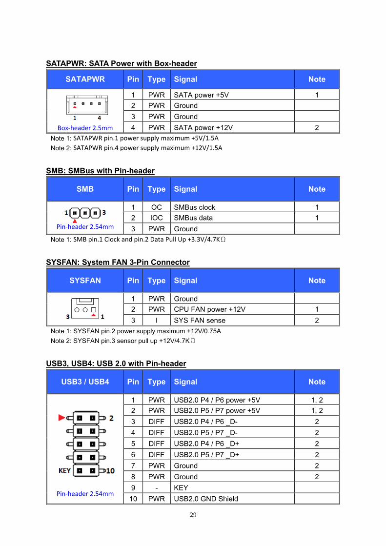
SATAPWR: SATA Power with Box-header
SATAPWR Pin Type Signal Note
Box‐header 2.5mm
1 PWR SATA power +5V 1
2 PWR Ground
3 PWR Ground
4 PWR SATA power +12V 2
Note 1: SATAPWR pin.1 power supply maximum +5V/1.5A
Note 2: SATAPWR pin.4 power supply maximum +12V/1.5A
SMB: SMBus with Pin-header
SMB Pin Type Signal Note
Pin‐header 2.54mm
1 OC SMBus clock 1
2 IOC SMBus data 1
3 PWR Ground
Note 1: SMB pin.1 Clock and pin.2 Data Pull Up +3.3V/4.7KΩ
SYSFAN: System FAN 3-Pin Connector
SYSFAN Pin Type Signal Note
1 PWR Ground
2 PWR CPU FAN power +12V 1
3 I SYS FAN sense 2
Note 1: SYSFAN pin.2 power supply maximum +12V/0.75A
Note 2: SYSFAN pin.3 sensor pull up +12V/4.7KΩ
USB3, USB4: USB 2.0 with Pin-header
USB3 / USB4 Pin Type Signal Note
Pin‐header 2.54mm
1 PWR USB2.0 P4 / P6 power +5V 1, 2
2 PWR USB2.0 P5 / P7 power +5V 1, 2
3 DIFF USB2.0 P4 / P6 _D- 2
4 DIFF USB2.0 P5 / P7 _D- 2
5 DIFF USB2.0 P4 / P6 _D+ 2
6 DIFF USB2.0 P5 / P7 _D+ 2
7 PWR Ground 2
8 PWR Ground 2
9 - KEY
10 PWR USB2.0 GND Shield

30
Note 1: USB3 and USB4 pin.1~2 power supply maximum +5V/0.5A
Note 2: For USB2.0 cabling it is required to use only Hi-Speed USB cable, specified in USB2.0
standard:
WEBCAM: Webcam with Box-header
WEBCAM Pin Type Signal Note
Box‐header 1.0mm
1 PWR WEBCAM power +5V 1
2 DIFF USB2.0 P8_D-
3 DIFF USB2.0 P8_D+
4 PWR Ground
5 NC Not connected
Note 1: WEBCAM pin.1 power supply maximum +5V/0.5A
LPC: Low Pin Count (LPC) with Pin-header - (reserved for debug)
LPC Pin Type Signal Note
Pin‐header 2.0mm
1 IOC LPC_AD0
2 OC LPC_PLTRST# 1
3 IOC LPC_AD1
4 OC LPC_FRAME#
5 IOC LPC_AD2
6 PWR LPC Power +3.3V
7 IOC LPC_AD3
8 PWR Ground
9 I LPC_Clock
10 - KEY
Note 1: LPC pin.2 LPC_PLTRST# pull up +3.3V/470Ω
Note 2: Reserved for debug with pin-header

31
SPI: Serial Peripheral Interface (SPI) with Pin-header - (reserved for debug)
SPI Pin Type Signal Note
Pin‐header 2.0mm
1 OC SPI_CS0#
2 PWR SPI power +1.8V
3 IOC SPI_MISO
4 IOC SPI_HOLD# 1
5 NC Not connected
6 OC SPI_CLOCK
7 PWR Ground
8 OC SPI_MOSI
Note 1: SPI pin.4 SPI_HOLD# pull up +1.8V/3.3KΩ
Note 2: Reserved for debug with pin-header

32
1.7 I/O ports power output (max.)
Rear I/O Ports Power Output (max.)
Rear I/O Port Name PortsPower output watts
(max.) Remark
COM Ports
(COM1_COM2) 2
+5V/1.0A 5.0W Power output voltage by
(JPCOMx) jumper select +12V/1.0A 12.0W
USB 2.0 Ports
(USB1_LAN1, USB2_LAN2) 3 +5V/0.5A 2.5W
USB 3.0 Port
(USB1_LAN1) 1 +5V/0.9A 4.5W
※1. WMX-J19000 M/B total +12V maximum power output watts = +12V/6A (72W)
※2. WMX-J19000 M/B total +5V maximum power output watts = +5V/10A (50W)
※3. WMX-J19000 M/B total +3.3V maximum power output watts = +3.3V/6A (19.8W)
On Board Expansion Slots Power Output (max.)
Expansion Slot Name PortsPower output watts
(max.) Remark
DDR3L SO-DIMM
(CHA-DIMM) 1
+1.35V/2.0A 2.7W
+0.675V/0.6A 0.405W
MiniPCIe / mSATA
(MINI-PCIE) 1
+3.3VS/1.1A 3.63W MINI-PCIE / mSATA function
by (JMINI-PCIE) jumper select+1.5V/0.375A 0.563W
Micro SD / T-Flash
(MICRO-SD) 1 +3.3V/0.1A 0.33W
PCIe x1
(PCIE) 1
+3.3VS/0.375A
25W
[1] Standard height = 25W
[2] Low profile card = 10W,
+12V = 0.5A
+3.3V/3.0A
+12V/2.1A
※1. WMX-J19000 M/B total +12V maximum power output watts = +12V/6A (72W)
※2. WMX-J19000 M/B total +5V maximum power output watts = +5V/10A (50W)
※3. WMX-J19000 M/B total +3.3V maximum power output watts = +3.3V/6A (19.8W)
On Board I/O Ports Power Output (max.)
Rear I/O Port Name PortsPower output watts
(max.) Remark
COM [Box-Header], pin.8 (COM3, COM4, COM5, COM6)
4 +5V/1.0A 5.0W Power output voltage by
(JPCOMx) jumper select +12V/1.0A 12.0W
CPU Fan [Pin-Header],
pin.2 (SYSTEM) 1 +12V/0.75A 9.0W

33
Rear I/O Port Name PortsPower output watts
(max.) Remark
Front Panel [Pin-Header],
pin.1 PWRLED (FRONT)
1
+5V/10mA 50mW Power On LED
Front Panel [Pin-Header],
pin.2 HDDLED (FRONT) +5V/10mA 50mW SATA HDD LED
Front Panel [Pin-Header],
pin.6 SUSLED (FRONT) +5VS/10mA 50mW Suspend LED
Front Panel [Pin-Header],
pin.16 (FRONT) +5V/100mA 0.5W
LVDS conn. [connector],
pin.27~30 (LVDS) 1
+3.3V/1.0A 3.3W Power output voltage by
(JPLVDS) jumper select
+5V/1.0A 5.0W Power output voltage by
(JPLVDS) jumper select
+12V/1.0A 12.0W Power output voltage by
(JPLVDS) jumper select
PS/2 KB and MS [connector],
pin.4 (KB_MS) 1 +5V/0.25A 1.25W PS/2 Keyboard and Mouse
SATA Power [Box-Header], pin.1= +5V, pin.4=+12V (SATAPWR)
1 +5V/1.5A 7.5W
+12V/1.5A 18.0W
System Fan [Pin-Header],
pin.2 (SYSTEM) 1 +12V/0.5A 6.0W
USB 2.0 [Pin-Header],
pin.1~1 (USB3, USB4) 4 +5V/0.5A 2.5W
WebCam [connector],
pin.1 (WEBCAN) 1 +5V/0.5A 2.5W
※1. WMX-J19000 M/B total +12V maximum power output watts = +12V/6A (72W)
※2. WMX-J19000 M/B total +5V maximum power output watts = +5V/10A (50W)
※3. WMX-J19000 M/B total +3.3V maximum power output watts = +3.3V/6A (19.8W)
34
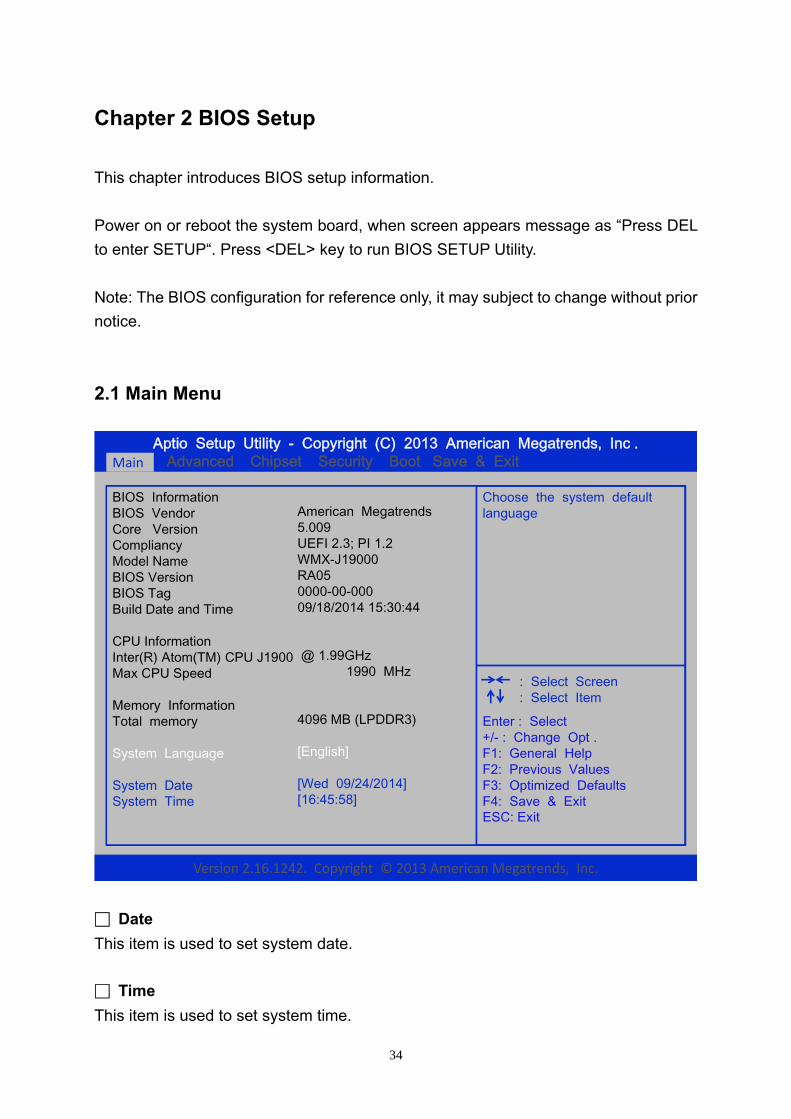
Chapter 2 BIOS Setup
This chapter introduces BIOS setup information.
Power on or reboot the system board, when screen appears message as “Press DEL
to enter SETUP“. Press <DEL> key to run BIOS SETUP Utility.
Note: The BIOS configuration for reference only, it may subject to change without prior
notice.
2.1 Main Menu
Aptio Setup Utility - Copyright (C) 2013 American Megatrends, Inc .Main Advanced Chipset Security Boot Save & Exit
BIOS InformationBIOS VendorCore VersionCompliancyModel NameBIOS Version BIOS TagBuild Date and Time
CPU InformationInter(R) Atom(TM) CPU J1900Max CPU Speed
Memory InformationTotal memory
System Language
System DateSystem Time
Choose the system defaultlanguage
Enter : Select+/- : Change Opt .F1: General HelpF2: Previous ValuesF3: Optimized DefaultsF4: Save & ExitESC: Exit
Main
: Select Screen: Select Item
American Megatrends5.009UEFI 2.3; PI 1.2WMX-J19000RA050000-00-00009/18/2014 15:30:44
@ 1.99GHz1990 MHz
4096 MB (LPDDR3)
[English]
[Wed 09/24/2014][16:45:58]
Version 2.16.1242. Copyright © 2013 American Megatrends, Inc.
Date This item is used to set system date. Time This item is used to set system time.

35
2.2 Advanced Menu
Aptio Setup Utility - Copyright (C) 2013 American Megatrends, Inc .Main Advanced Chipset Security Boot Save & Exit
Set ERP mode in ACPI S4/S5
Enter : Select+/- : Change Opt .F1: General HelpF2: Previous ValuesF3: Optimized DefaultsF4: Save & ExitESC: Exit
Advanced
: Select Screen: Select Item
ERPWake upResume By RTC AlarmOS SelectionLPSS & SCC Devices ModeACPI SettingsF81866 Super IO ConfigurationHardware MonitorCPUIDENetworkCSMUSB
[Disabled][Enabled][Disabled][Windows 7][ACPI mode]
Version 2.16.1242. Copyright © 2013 American Megatrends, Inc.
ConfigurationConfigurationStack ConfigurationConfigurationConfiguration
ERP This item is used to enable or disable ERP.
The optional settings are:
[ERP/EUP +WOL (LAN1)], [ERP/EUP (Fintek G3)], [Disable]
This item should be set as [Disabled] if users want to active all Wake-up functions.
Wake up This item is used to enable or disable Wake up. Reseume By RTC Alarm This item is used to enable or disable Reseume By RTC Alarm. OS Selection The optional settings are: [Windows7], [Windows8.x], [Android]

36
LPSS & SCC Devices Mode This item is used to select the LPSS and SCC device mode as ACPI or PCI mode.

37
2.3 ACPI Settings
Aptio Setup Utility - Copyright (C) 2013 American Megatrends, Inc .
ACPI Settings
Enable ACPI Auto ConfigurationACPI Sleep State
Enables or Disables BIOS ACPI Auto Configuration
Enter : Select+/- : Change Opt .F1: General HelpF2: Previous ValuesF3: Optimized DefaultsF4: Save & ExitESC: Exit
Advanced
: Select Screen: Select Item
[Disabled][S3 (Suspend to RAM)]
Version 2.16.1242. Copyright © 2013 American Megatrends, Inc.
Enabled ACPI Auto Configuration The item is used to enable or disable the ACPI Auto Configuration. Choices: Disabled, Enabled.
ACPI Sleep State Select the ACPI sleep state and the system will enter when SUSPEND button is
pressed.

38
2.4 Super IO Configuration
Aptio Setup Utility - Copyright (C) 2013 American Megatrends, Inc .
F81866 Super IO ConfigurationSet Parameters of Serial Port1 (COMA)
Enter : Select+/- : Change Opt .F1: General HelpF2: Previous ValuesF3: Optimized DefaultsF4: Save & ExitESC: Exit
Advanced
: Select Screen: Select Item
F81866
Version 2.16.1242. Copyright © 2013 American Megatrends, Inc.
Super IO ChipSerial Port 1 ConfigurationSerial Port 2 ConfigurationSerial Port 3 ConfigurationSerial Port 4 ConfigurationSerial Port 5 ConfigurationSerial Port 6 ConfigurationWatch dog timerWatch dog timer counter
[Disabled]10
Serial Port 1 Configuration Serial Port 2 Configuration Serial Port 3 Configuration Serial Port 4 Configuration Serial Port 5 Configuration Serial Port 6 Configuration

39
watch dog timer The item is used to determine watch dog timer.

40
2.5 Serial Port 1 Configuration
Aptio Setup Utility - Copyright (C) 2013 American Megatrends, Inc .
Serial Port 1 Configuration
Serial Port [Enabled]Device Settings IO=3F8h; IRQ=4;
Change Settings [Auto]
Enable or Disable Serial Port (COM)
Enter : Select+/- : Change Opt .F1: General HelpF2: Previous ValuesF3: Optimized DefaultsF4: Save & ExitESC: Exit
Advanced
: Select Screen: Select Item
Version 2.16.1242. Copyright © 2013 American Megatrends, Inc.
Serial Port The item is used to enable or disable the serial port.
Device Settings The item is used to show the serial port IO port address and interrupt address. Change Settings The item is used to change COM address as required.

41
2.6 Serial Port 2 Configuration
Aptio Setup Utility - Copyright (C) 2013 American Megatrends, Inc .
Serial Port 2 Configuration
Serial Port [Enabled]Device Settings IO=2F8h; IRQ=3;
Change Settings [Auto]Serial port Mode [Pure RS-232]
Enable or Disable Serial Port (COM)
Enter : Select+/- : Change Opt .F1: General HelpF2: Previous ValuesF3: Optimized DefaultsF4: Save & ExitESC: Exit
Advanced
: Select Screen: Select Item
Version 2.16.1242. Copyright © 2013 American Megatrends, Inc. Serial Port The item is used to enable or disable the serial port.
Device Settings The item is used to show the serial port IO port address and interrupt address. Change Settings The item is used to change COM address as required.
Serial Port Mode The item is used to select Serial port Mode for RS-232/422/485.

42
2.7 Serial Port 3 Configuration
Aptio Setup Utility - Copyright (C) 2013 American Megatrends, Inc .
Serial Port 3 Configuration
Serial Port [Enabled]Device Settings IO=3E8h; IRQ=5;
Change Settings [Auto]
Enable or Disable Serial Port (COM)
Enter : Select+/- : Change Opt .F1: General HelpF2: Previous ValuesF3: Optimized DefaultsF4: Save & ExitESC: Exit
Advanced
: Select Screen: Select Item
Version 2.16.1242. Copyright © 2013 American Megatrends, Inc.
Serial Port The item is used to enable or disable the serial port.
Device Settings The item is used to show the serial port IO port address and interrupt address. Change Settings The item is used to change COM address as required

43
2.8 Serial Port 4 Configuration
Aptio Setup Utility - Copyright (C) 2013 American Megatrends, Inc .
Serial Port 4 Configuration
Serial Port [Enabled]Device Settings IO=2E8h; IRQ=5;
Change Settings [Auto]
Enable or Disable Serial Port (COM)
Enter : Select+/- : Change Opt .F1: General HelpF2: Previous ValuesF3: Optimized DefaultsF4: Save & ExitESC: Exit
Advanced
: Select Screen: Select Item
Version 2.16.1242. Copyright © 2013 American Megatrends, Inc.
Serial Port The item is used to enable or disable the serial port.
Device Settings The item is used to show the serial port IO port address and interrupt address. Change Settings The item is used to change COM address as required

44
2.9 Serial Port 5 Configuration
Aptio Setup Utility - Copyright (C) 2013 American Megatrends, Inc .
Serial Port 5 Configuration
Serial Port [Enabled]Device Settings IO=3E0h; IRQ=5;
Change Settings [Auto]
Enable or Disable Serial Port (COM)
Enter : Select+/- : Change Opt .F1: General HelpF2: Previous ValuesF3: Optimized DefaultsF4: Save & ExitESC: Exit
Advanced
: Select Screen: Select Item
Version 2.16.1242. Copyright © 2013 American Megatrends, Inc.
Serial Port The item is used to enable or disable the serial port.
Device Settings The item is used to show the serial port IO port address and interrupt address. Change Settings The item is used to change COM address as required

45
2.10 Serial Port 6 Configuration
Aptio Setup Utility - Copyright (C) 2013 American Megatrends, Inc .
Serial Port 6 Configuration
Serial Port [Enabled]Device Settings IO=2E0h; IRQ=5;
Change Settings [Auto]
Enable or Disable Serial Port (COM)
Enter : Select+/- : Change Opt .F1: General HelpF2: Previous ValuesF3: Optimized DefaultsF4: Save & ExitESC: Exit
Advanced
: Select Screen: Select Item
Version 2.16.1242. Copyright © 2013 American Megatrends, Inc.
Serial Port The item is used to enable or disable the serial port.
Device Settings The item is used to show the serial port IO port address and interrupt address. Change Settings The item is used to change COM address as required

46
2.11 PC Health Satus
Aptio Setup Utility - Copyright (C) 2013 American Megatrends, Inc .
PC Health Status
Smart Fan FunctionSmart Fan Mode Configuration
Enter : Select+/- : Change Opt .F1: General HelpF2: Previous ValuesF3: Optimized DefaultsF4: Save & ExitESC: Exit
Advanced
: Select Screen: Select Item
: +39 C: +34 C: 4823RPM: N/A: +0.908 V: +1.360V: +5.045V: +11.528V: +3.424V: +3.344V: +5.040V: +3.200V
[Enabled]
Enable or Disable Smart Fan
Version 2.16.1242. Copyright © 2013 American Megatrends, Inc.
CPUSYSCPUSYSCPUDDR3L+V5+V12VCC3VVSB3VVSB5VVBAT
TempTempFan SpeedFan Speed
Smart Fan Function The item allows users to enable or disable the System smart fan feature. Smart Fan Mode Configuration This item is used to set the smart fan mode.

47
2.12 Smart Fan Mode Configuration
Aptio Setup Utility - Copyright (C) 2013 American Megatrends, Inc .
Smart Fan Mode Select
Enter : Select+/- : Change Opt .F1: General HelpF2: Previous ValuesF3: Optimized DefaultsF4: Save & ExitESC: Exit
Advanced
: Select Screen: Select Item
Version 2.16.1242. Copyright © 2013 American Megatrends, Inc.
Smart Fan Mode Configuration
CPU FAN Smart Fan ControlTemperature 1Temperature 2Temperature 3Temperature 4Duty Cycle 1Duty Cycle 2Duty Cycle 3Duty Cycle 4SYS FAN Smart Fan ControlTemperature 1Temperature 2Temperature 3Temperature 4Duty Cycle 1Duty Cycle 2Duty Cycle 3Duty Cycle 4
[Auto Duty-Cycle Mode]6050403085706050[Auto Duty-Cycle Mode]6050403085706050
CPU Fan Smart Fan Control The item is used to enable or disable the CPU smart fan feature.
SYS Fan Smart Fan Control The item is used to enable or disable the SYS smart fan feature.

48
2.13 CPU Configuration
Aptio Setup Utility - Copyright (C) 2013 American Megatrends, Inc .
Enter : Select+/- : Change Opt .F1: General HelpF2: Previous ValuesF3: Optimized DefaultsF4: Save & ExitESC: Exit
Advanced
: Select Screen: Select Item
CPU Configuration
Intel(R) Atom(TM) CPU E3845 @ 1.91GHzCPU SignatureMicrocode PatchMax CPU SpeedMin CPU SpeedProcessor CoresIntel HT TechnologyIntel VT-x Technology
L1 Data CacheL1 Code CacheL2 CacheL3 Cache
306733211910 MHZ500 MHz4Not SupportedSupported
24 kB x 432 kB x 41024 kB x 2Not Present
Version 2.16.1242. Copyright © 2013 American Megatrends, Inc.

49
2.14 IDE Configuration
Aptio Setup Utility - Copyright (C) 2013 American Megatrends, Inc .
IDE Configuration
Serial-ATA (SATA)
SATA Speed SupportSATA ODD PortSATA Mode
Serial-ATA Port 0
mSATA
SATA Port0Not Present
mSATANot Present
Enable / disable Serial ATA
Enter : Select+/- : Change Opt .F1: General HelpF2: Previous ValuesF3: Optimized DefaultsF4: Save & ExitESC: Exit
Advanced
: Select Screen: Select Item
[Enabled]
[Gen2][No ODD][AHCI Mode]
[Enabled]
[Enabled]
Version 2.16.1242. Copyright © 2013 American Megatrends, Inc. Serial-ATA (SATA) The item is used to enable or disable the SATA device. SATA Speed Support The item configures SATA controller to Gen1 or Gen2 speed. SATA ODD Port SATA ODD is Port0 or Port1.
SATA Mode The item is used to disable or set the chip in serial SATA controller mode.
Choices: Disable, IDE, AHCI. Serial-ATA Port 0 The item is used to enable or disable SATA port 0.

50
mSATA The item is used to enable or disable mSATA.

51
2.15 Network Stack Configuration
Aptio Setup Utility - Copyright (C) 2013 American Megatrends, Inc .
Network Stack Enable/Disable UEFI Network Stack
Enter : Select+/- : Change Opt .F1: General HelpF2: Previous ValuesF3: Optimized DefaultsF4: Save & ExitESC: Exit
Advanced
: Select Screen: Select Item
[Disabled]
Version 2.16.1242. Copyright © 2013 American Megatrends, Inc.
Network Stack The item is used to enable or disable UEFI Network Stack.

52
2.16 Compatibility Support Module Configuration
Aptio Setup Utility - Copyright (C) 2013 American Megatrends, Inc .
Compatibility Support Module Configuration
CSM Support
GateA20 ActiveOption ROM MessagesINT19 Trap Response
Boot option filter
Option ROM execution
NetworkStorageVideoOther PCI devices
Enables /Disable CSM Support
Enter : Select+/- : Change Opt .F1: General HelpF2: Previous ValuesF3: Optimized DefaultsF4: Save & ExitESC: Exit
Advanced
: Select Screen: Select Item
[DO not launch][UEFI][Legacy][UEFI]
[Enabled]
[Upon Request][Force BIOS][Immediate]
[UEFI and Legacy]
Version 2.16.1242. Copyright © 2013 American Megatrends, Inc.
CSM Support The item is used to enable or disable Compatibility Support Module Configuration. GateA20 Active The item is used to control GateA20 can be disabled or not. Option ROM Messages Set display mode for Option ROM. INT 19 Trap Response The item is used to control BIOS reaction on INT19 trapping, default setting is
Immediate.
Boot option filter The item is used to control Legacy/UEFI ROMs priority.

53
Network The item is used to control the execution of UEFI and Legacy PXE OpROM. Storage The item is used to control the execution of UEFI and Legacy Storage OpROM. Video The item is used to control the execution of UEFI and Legacy Video OpROM.
Other PCI devices The item is used to determine OpROM execution policy for devices other than
Network, Storage or Video.

54
2.17 USB Configuration
Aptio Setup Utility - Copyright (C) 2013 American Megatrends, Inc .
USB Configuration
USB Devices:1 Keyboard, 1 Mouse, 3 Hubs
Legacy USB SupportXHCI Hand-offEHCI Hand-offUSB Mass Storage Driver Support
USB hardware delays and time-outs:USB transferDevice resetDevice power-up delay
Enables Legacy USB supportAUTO option disables legacysupport if no USB devices are connected. DISABLE option willkeep USB devices availableOnly for EFI applications.
Enter : Select+/- : Change Opt .F1: General HelpF2: Previous ValuesF3: Optimized DefaultsF4: Save & ExitESC: Exit
Advanced
: Select Screen: Select Item
[20 sec][20 sec][Auto]
[Enabled][Enabled][Disabled][Enabled]
Version 2.16.1242. Copyright © 2013 American Megatrends, Inc.
time-outtime-out
Legacy USB Support The item is used to enable or disable legacy support about USB devices.
Choices: Disabled, Enabled, Auto.
USB3.0 Support The item is used to enable or disable USB3.0 (XHCI) controller support. Choices: Disabled, Enabled. XHCI Hand-off The item is workaround for OSes without XHCI hand-off support. Choices: Disabled, Enabled. EHCI Hand-off The item is a workaround for OSes without EHCI hand-off support. Choices: Disabled, Enabled.

55
USB Transfer time-out The item is for the time-out value for Control, Bulk, and Interrupt transfers.
Device reset time-out The item is for USB mass storage device start unit command time-out. Device power-up delay The item is for maximum time and the device will take before it properly reports itself
to the host controller.

56
2.18 Chipset
Aptio Setup Utility - Copyright (C) 2013 American Megatrends, Inc .Main Advanced Chipset Security Boot Save & Exit
Enable/Disable LAN1.
Enter : Select+/- : Change Opt .F1: General HelpF2: Previous ValuesF3: Optimized DefaultsF4: Save & ExitESC: Exit
: Select Screen: Select Item
LAN1LAN2MINI-PCIENorth BridgeSouth Bridge
Chipset
Version 2.16.1242. Copyright © 2013 American Megatrends, Inc.
[Enabled][Enabled][Enabled]
LAN1 The item is used to enable or disable LAN1. LAN2 The item is used to enable or disable LAN2. MINI-PCIE The item is used to enable or disable MINI-PCIE.

57
2.19 Memory Information
Aptio Setup Utility - Copyright (C) 2013 American Megatrends, Inc .Main Advanced Chipset Security Boot Save & Exit
Config Intel IGD Settings.
Enter : Select+/- : Change Opt .F1: General HelpF2: Previous ValuesF3: Optimized DefaultsF4: Save & ExitESC: Exit
: Select Screen: Select Item
Intel IGD Configuration
Memory InformationTotal Memory
Max TOLUD
Chipset
4096 MB (LPDDR3)
[Dynamic]
Version 2.16.1242. Copyright © 2013 American Megatrends, Inc.
Max TOLUS The item is used to allow users to configure the maximum TOLUD value.

58
2.20 Intel IGD Configuration
Aptio Setup Utility - Copyright (C) 2013 American Megatrends, Inc .Main Advanced Chipset Security Boot Save & Exit
Enable : Enable IntegratedGraphics Device (IGD) whenselected as the Primary Video Adaptor.Disable: Alwaysdisbale IGD
Enter : Select+/- : Change Opt .F1: General HelpF2: Previous ValuesF3: Optimized DefaultsF4: Save & ExitESC: Exit
: Select Screen: Select Item
Intel IGD ConfigurationIntegrated Graphics Device
IGD Turbo EnablePrimary DisplayGFX BoostPAVCDVMT Pre-AllocatedDVMT Total Gfx MemAperture SizeDOP CGGTT Size
ISP Enabled/DisableISP PCI Device Selection
Primary IGFX Boot DisplayBacklight ControlLVDSBacklight Active ModeBacklight Voltage LevelBacklight Control Level
Chipset
[Enabled]
[Enabled][IGD][Disabled][LITE Mode][64M][256MB][256MB][Enabled][2MB]
[Enabled][Disabled]
[VBIOS Default][PWM Normal][Enabled][DC Mode][+3.3V][Step 10]
Version 2.16.1242. Copyright © 2013 American Megatrends, Inc. Integrated Graphics Device The item is used to enable or disable Integrated Graphics Device. IGD Turbo Enable The item is used to enable or disable Integrated IGD Turbo. Primary Display The item is used to indicate Graphics device. GFX Boost The item is used to enable or disable GFX Boost. PAVC The item is used to enable or disable Protect Audio Video Control.

59
DVMT Pre-Allocated The item is used to select DVMT 5.0 Pre-Allocated (Fixed) Graphics Memory size
used by Internal Graphics Device. DVMT Total Gfx Mem The item is used to select DVMT 5.0 Total Graphics Memory size used by Internal
Graphics Device. Aperture Size The item is used to select Aperture Size. DOP CG The item is used to enable or disable DOP CG. GTT Size The item is used to select GTT Size. ISP Enable/Disable The item is used to enable or disable ISP. ISP PCI Device Selection The item is used to enable or disable ISP PCI Device Selection. Primary IGFX Boot Display The item is used to select the display device which will be activated during POST.
Backlight Control The item is used to display Backlight Control setting. LVDS The item is used to enable or disable LVDS. Backlight Active Mode Choices: PWN Mode, DC Mode. Backlight Voltage Level Choices: +3.3V, +5V

60
Backlight Control Level Choices: Step1, Step2, Step3, Step4, Step5, Step6, Step7, Step8, Step9, Step10

61
2.21 USB Configuration
Aptio Setup Utility - Copyright (C) 2013 American Megatrends, Inc .Main Advanced Chipset Security Boot Save & Exit
USB Configuration Settings
Enter : Select+/- : Change Opt .F1: General HelpF2: Previous ValuesF3: Optimized DefaultsF4: Save & ExitESC: Exit
: Select Screen: Select Item
USB ConfigurationPCI Express Configuration
Chipset
Version 2.16.1242. Copyright © 2013 American Megatrends, Inc.
USB Configuration PCI Express Configuration

62
2.22 XHCI Mode
Aptio Setup Utility - Copyright (C) 2013 American Megatrends, Inc .
USB ConfigurationXHCI ModeUSB2 Link Power Management
USB 2.0(EHCI) Support
Mode of operation of xHCIcontroller
Enter : Select+/- : Change Opt .F1: General HelpF2: Previous ValuesF3: Optimized DefaultsF4: Save & ExitESC: Exit
Chipset
: Select Screen: Select Item
[Auto][Disabled]
[Disabled]
Version 2.16.1242. Copyright © 2013 American Megatrends, Inc.
XHCI Mode The item is used to allow users to determine the operation mode for the XHCI
controller in OS. USB2 Link Power Management The item is used to enable or disable USB2 Link Power Management. USB 2.0(EHCI) Support The item is used to enable or disable USB 2.0(EHCI) Support.

63
2.23 PCI Express Configuration
Aptio Setup Utility - Copyright (C) 2013 American Megatrends, Inc .
PCI Express ConfigurationMINI-PCIE
Speed
PCIESpeed
Enable or Disable theMINI-PCIE in Chipset
Enter : Select+/- : Change Opt .F1: General HelpF2: Previous ValuesF3: Optimized DefaultsF4: Save & ExitESC: Exit
Chipset
: Select Screen: Select Item
[Enabled][Auto]
[Enabled][Auto]
Version 2.16.1242. Copyright © 2013 American Megatrends, Inc.
MINI-PCIE The item is used to enable or disable MINI-PCIE. Speed The item is used to select Speed. PCIE The item is used to enable or disable PCIE. Speed The item is used to select Speed.

64
2.24 Password Configuration
Aptio Setup Utility - Copyright (C) 2013 American Megatrends, Inc .Main Advanced Chipset Security Boot Save & Exit
Password DescriptionIf ONLY the Administrator’s password is set ,then this only limits access to Setup and isonly asked for when entering SetupIf ONLY the User’s password is set, then thisis a power on password and must be entered toboot or enter Setup. In Setup the User willhave Administrator rights.The password length must be in the following range:Minimum length 3Maximum length 20
Administrator PasswordUser Password
Set Administrator Password
Enter : Select+/- : Change Opt .F1: General HelpF2: Previous ValuesF3: Optimized DefaultsF4: Save & ExitESC: Exit
: Select Screen: Select Item
Security
Version 2.16.1242. Copyright © 2013 American Megatrends, Inc.

65
2.25 Boot Configuration
Aptio Setup Utility - Copyright (C) 2013 American Megatrends, Inc .Main Advanced Chipset Security Boot Save & Exit
Boot ConfigurationSetup Prompt Timeout Bootup NumLock State
Quiet BootFast Boot
Boot Option Priorities
Number of seconds to wait forsetup activation key.65535(0xFFFF) means indefinitewaiting.
Enter : Select+/- : Change Opt .F1: General HelpF2: Previous ValuesF3: Optimized DefaultsF4: Save & ExitESC: Exit
: Select Screen: Select Item
Boot
2[On]
[Disabled][Disabled]
Version 2.16.1242. Copyright © 2013 American Megatrends, Inc.
Bootup NumLock State The item is used to make NumLock auto-operate. Quiet Boot The item is used to enable or disable the Quiet Boot function. Fast Boot The item is used to enable or disable the Fast Boot function. Boot Option Priorities The item is used to show the priorities of the boot options.

66
2.26 Save Changes and Exit
Aptio Setup Utility - Copyright (C) 2013 American Megatrends, Inc .Main Advanced Chipset Security Boot Save & Exit
Save Changes and ExitDiscard Changes and ExitSave Changes and ResetDiscard Changes and Reset
Restore Defaults
Boot Override
Launch EFI Shell from filesystem device
Exit system setup after saving the changes.
Enter : Select+/- : Change Opt .F1: General HelpF2: Previous ValuesF3: Optimized DefaultsF4: Save & ExitESC: Exit
: Select Screen: Select Item
Save & Exit
Version 2.16.1242. Copyright © 2013 American Megatrends, Inc.
Save Changes and Exit Exit system setup after saving the changes.
Discard Changes and Exit Exit system setup without saving the changes.
Save Changes and Reset Reset the system after saving the changes.
Discard Changes and Exit Reset system setup without saving any changes.
Save Changes Save changes for setup options.

67
Discard Changes Discard changes for setup options.
Restore Defaults Restore/Load Defaults values for all the setup options.
Save User Defaults Save the changes for User Defaults.
Restore User Defaults Restore the User Defaults to all the setup options.

68
Chapter 3 Drivers Installation
This chapter introduces driver installation information.
Please insert the utility CD to CD-ROM drive, the install menu will appear
automatically, if the install menu does not list suitable driver of Operate System or
appear automatically, please select corresponding driver of utility CD to install.
The Windows XP driver installation steps are as below.
3.1 Intel Chipset Device Software
Step1: Click “Next” to continue.

69
Step 2: Read the License Agreement and click “Accept” to continue.
Step 3: Click “Install” to continue.

70
Step 4: Click “Finish” to complete setup.

71
3.2 Intel Graphic Media Accelerator Driver Step 1: Click “Next” to continue.
Step 2: Click “No” to continue.

72
Step 3: Click “Next” to continue.
Step 4: Click “Next” to continue.

73
Step 5: Click “Finish” to complete setup.

74
3.3 LAN Driver Step 1: Click “Next” to continue.
Step 2: Click “Next” to continue.

75
Step 3: Click “Next” to continue
Step 4: Click “Install” to continue.

76
Step 5: Click “Finish” to complete setup.

77
3.4 Audio Driver Step 1: Click “Next” to continue.
Step 2: Click “Finish” to complete setup.

78
3.5 TXE Driver Step 1: Click “Yes” to continue. (optional for Win7)
Step 2: Click “Close” to complete setup. (optional for Win7)

79
Step 3: Click “Next” to continue.
Step 4: Click “Next” to continue.

80
Step 5: Click “Next” to continue.
Step6: Click “Finish” to complete setup..

81
3.6 USB Driver Step 1: Click “Next” to continue.
Step 2: Click “No” to continue.

82
Step 3: Click “Next” to continue.

83
Appendix A: Watchdog Timer
The working algorithm of the WDT function can be simply described as a counting
process. The Time-Out Interval can be set through software programming. The
availability of time-out interval is set by software.
The System Board allows users control WDT through dynamic software programming.
The WDT starts counting when it is activated. It sends out a signal to system reset,
when time-out interval ends. To prevent the time-out interval from running out, a
re-trigger signal will need to be sent before the counting reaches its end. This action
will restart the counting process.
WDT program should keep the counting process running under normal condition.
WDT should never generate a system reset unless the system runs into troubles.
The related Control Registers of WDT are all included in the following sample program
that is written in C language. User can fill a non-zero value into the Time-out Value
Register to enable/refresh WDT. System will be reset after the Time-out Value to be
counted down to zero. Or user can directly fill a zero value into Time-out Value
Register to disable WDT immediately.
To ensure a successful accessing to the content of desired Control Register, the
sequence of following program codes should be step-by-step run again when each
register is accessed.
For more information about WDT, please refer to Fintek F81866A data sheet.
There are two PnP I/O port addresses that can be used to configure WDT,
1) 0x2E:EFIR (Extended Function Index Register, for identifying CR index number)
2) 0x2F:EFDR (Extended Function Data Register, for accessing desired CR)
Below are some example codes, which demonstrate the use of WDT.

84
// Enter Extended Function Mode
outp(0x2E, 0x87);
outp(0x2E, 0x87);
// Select Logic Device 7
outp(0x2E, 0x07);
outp(0x2F, 0x07);
// Select & Enable GPIO1
outp(0x2E, 0x27);
outp(0x2F, inp(0x2F) | 0x05);
// Assign Pin 70 to be a WDTO# Signal
outp(0x2E, 0x2C);
outp(0x2F, inp(0x2F) & 0xDF);
//Clear WDTO# Status
outp(0x2E, 0xF5);
outp(0x2F, inp(0x2F) | 0x40);
// Select time unit (Second )
outp(0x2E, 0xF5);
outp(0x2F, inp(0x2F) & Count-mode Register);
// Select time unit (Minute)
outp(0x2E, 0xF5);
outp(0x2F, inp(0x2F) | Count-mode Register);
// Set Time-out Value
outp(0x2E, 0xF6);
outp(0x2F, Time-out Value Register );
// Counting of watchdog time is enable.
outp(0x2E, 0xF5);
outp(0x2F, inp(0x2F) | 0x20);
// Exit Extended Function Mode
outp(0x2E, 0xAA);

85
Definitions of Variables: Value of Count-mode Register :
1) 0x00 -- Count down in seconds (Bit3=0)
2) 0x08 -- Count down in minutes (Bit3=1)
Value of Time-out Value Register :
1) 0x00 -- Time-out Disable
2) 0x01~0xFF -- Value for counting down

86
Appendix B: GPIO
The System Board provides 4 dedicated output ports and 4 programmable I/O ports
that can be individually configured to perform a simple I/O function. Users can
configure 4 programmable I/O ports to become an input or output port by
programming register bit of I/O Selection .To invert port value, the setting of Inversion
Register has to be made (Note). Port values can be set to read or write through Data
Register.
Note: Only 4 programmable I/O ports support.
Additionally, 4 Digital Output ports amplified signals from GPIO ports. There are
open-drain buffers, which can offer greater driving capacity up to 100mA.
For more information about GPIO, please refer to Fintek F81866A data sheet.
The related Control Registers of GPIO are all included in the following sample
program that is written in C language. To ensure a successful accessing to the content
of desired Control Register, the sequence of following program codes should be
step-by-step run again when each register is accessed.
There are two PnP I/O port addresses that can be used to configure GPIO ports,
1) 0x2E - EFER (Extended Function Enable Register, for entering Extended Function
Mode)
- EFIR (Extended Function Index Register, for identifying CR index number)
2) 0x2F - EFDR (Extended Function Data Register, for accessing desired CR)
Below are some example codes, which demonstrate the use of GPIOs.

87
// Enter Extended Function Mode
outp(0x2E, 0x87);
outp(0x2E, 0x87);
// Assign Pin111-118 to be GPIO port
outp(0x2E, 0x27);
outp(0x2F, inp(0x2F) & 0xF3);
outp(0x2E, 0x28);
outp(0x2F, inp(0x2F) | 0x20);
// Select Logic Device 6
outp(0x2E, 0x07);
outp(0x2F, 0x06);
// Enable GPIO Port
outp(0x2E, 0x30);
outp(0x2F, 0x01);
// Select GPIO Input / Output Mode
// default GPIO87/86/85/84 as Output pin, GPIO83/82/81/80 as Input pin.
outp(0x2E, 0x88);
outp(0x2F, (inp(0x2F) | 0xF0));
// Access Output value
outp(0x2E, 0x89);
outp(0x2F, (inp(0x2F) | Output Data));
// Read Input value
outp(0x2E, 0x8A);
Input Data = inp(0x2F);
// Exit Extended Function Mode
outp(0x2E, 0xAA);

88
Definitions of Variables: Each bit in the lower nibble of each Register represents the setting of a GPIO port.
Super IO Pin Pin Name Bit GPIO DIO 111 GPIO80 0 GPIO DIO-In0
112 GPIO81 1 GPIO DIO-In1
113 GPIO82 2 GPIO DIO-In2
114 GPIO83 3 GPIO DIO-In3
115 GPIO84 4 GPIO DIO-Out0
116 GPIO85 5 GPIO DIO-Out1
117 GPIO86 6 GPIO DIO-Out2
118 GPIO87 7 GPIO DIO-Out3
Value of Output Data / Input Data :
If a port is assigned to be an output port, then its respective bit can be
read/written.
If a port is assigned to be an input port, then its respective bit can be read only.
Note :
DIO-IN0/DIO-IN1/DIO-IN2/DIO-IN3 are programmed as Inputs by BIOS default.
Parameter Conditions
VinH min +1.857V
VinL max +0.525V
Rated Vin -8V ~ +12V
NC Status High by Default
** Attention : If DIO-IN0/DIO-IN1/DIO-IN2/DIO-IN3 are programmed as Output signal, they can only offer a normal signal transfer.(NOT amplified signals.)
Parameter Conditions
VoutH 3.3V thru 10k
VoutL 0V thru 1k
DIO-OUT0/DIO-OUT1/DIO-OUT2/DIO-OUT3 are fixed as Outputs by BIOS.
Parameter Conditions
Open-drain buffer Power-on default = Open
Driving Capacity max 100mA continue