word lab template 2002.08 - rochester institute of … · set_false_path) multiple clocks and...
TRANSCRIPT

Multiple Clocks and
10This lab is intended to give you a better understanding of how static timing analysis works and how timing exceptions are properly applied.
After completing this lab, you should be able to:
• Fully constrain and analyze a design using a minimum number of timing exceptions (set_max_delay, set_multicycle_path, set_false_path)
Timing Exceptions
Learning Objectives
Lab Duration: 60 minutes
Multiple Clocks and Timing Exceptions Lab 10-1 Synopsys 31833-000-S38

Lab 10
Background
The design you will be working with, called “test”, contains parallel paths shown in the figure below (resets not shown). Between inputs adr_i and coeff, and output dout there is a purely combinatorial path as well as a sequential path. The combinatorial and sequential paths actually have different constraints, and meet all setup and hold timing constraints. When you perform timing analysis, however, you will discover that there are initially many violations – all due to incomplete or incorrect constraints. This is not a trivial matter to correct.
clk
CombinatorialLogic
adr_i[15:0]
coeff[15:0]
sel_combo
dout[31:0]
mul_result_reg
Design “test”
This lab will step you through all the issues associated with constraining parallel sequential and combinatorial paths. You will also be shown an example of what does not work and why (set_max_delay).
Task 1. Read Mapped Design
1. Make sure your current working directory is risc_design and invoke dc_shell-t.
2. Read the previously compiled design “test” into memory.
read_db mapped/test.db current_design test link
3. Check the design’s timing constraints.
report_timing
Question 1. Is there anything unusual? ....................................................................................................
Lab 10-2 Multiple Clocks and Timing Exceptions Synopsys CHIP Synthesis Workshop

Lab 10
Task 2. Constrain the Design for Timing
There are no constraints set on the design; you need to apply a constraint script. The timing specifications for the design are as follows:
• Clock period: 200 MHz
• Input delays on data inputs (adr_i[*] and coeff[*]): 2 ns relative to the external system clock
• Input delay on sel_combo: 0.35 ns relative to external system clock
• Output delay: 4 ns relative to the external system clock
1. A constraint script with the above specifications has been created for your use. Apply the constraint file lab10_constraints.tcl and check the constraints.
source –echo –verbose lab10_constraints.tcl
report_clock
check_timing
report_timing
Question 2. How large is the worst negative slack? ....................................................................................................
Question 3. What path exhibits this violation? ....................................................................................................
Multiple Clocks and Timing Exceptions Lab 10-3 Synopsys CHIP Synthesis Workshop

Lab 10
Task 3. Using a Max-Delay Constraint
The violation you just discovered is very large. There are two possibilities, either the violations are real or the constraints specified were incorrect or insufficient.
From the timing report analyze the constraints placed on critical path in more detail.
Question 4. When does the data arrive at the input port? ....................................................................................................
Question 5. When is the data expected at the output port? ....................................................................................................
Question 6. What is the maximum path delay constraint for this critical path? ....................................................................................................
It is pretty clear that this path is over constrained - there is no way it can meet a –1 ns maximum delay!!
The designer of this block did not give you the proper information, go back to the designer and explain the situation: You find out that the maximum propagation delay through the combinational path should be constrained to 10 ns. This means that the constraints have to be adjusted.
During lecture you learned that set_multicycle_path and set_false_path, are considered to be “exceptions.” If you were to read through the Synopsys documentation you would find two other exception commands, set_max_delay and set_min_delay. Look at the man-pages for the set_max_delay command for further details.
Read the command description; it looks like you found a useful command to constrain your combinatorial path! Try it out…
(You will in fact discover in Task 4 that this command exhibits unexpected behavior, you will need to find a better solution).
Lab 10-4 Multiple Clocks and Timing Exceptions Synopsys CHIP Synthesis Workshop

Lab 10
1. Apply the appropriate max delay constraint on the combinational path.
set_max_delay 10 –from [get_ports "coeff* adr_i*"] \
-to [all_outputs]
Since set_max_delay is an exception, you should always make sure that the exception was actually applied correctly and that no exceptions were ignored.
check_timing
report_timing_requirements –ignored
You will notice a large number of exceptions that are being reported as ignored (non-existent paths). If you look closely, you will see that Design Compiler applied exceptions to paths that do not exist: e.g. Bit 1 of an input port to bits 2 and higher on the output port. Input bit 1 only connects to output bit 1.
The command applies the exception to all the permutations of the first argument with the second argument, whether the paths exist or not. If the buses were wider, thereby creating many more ignored exceptions, this would start to impact optimization run time. You would need to write the exceptions differently so that they contain only the actual paths. This is a small design and run time is not a concern here; you can ignore the non-existent paths.
2. Generate another timing report.
report_timing
It looks like this has solved the combinatorial delay problem. The critical path is no longer the combinatorial path
Question 7. Which path is the worst violator now? (Hint: Register reference names always end with “_reg[bit_#]” ) ....................................................................................................
Multiple Clocks and Timing Exceptions Lab 10-5 Synopsys CHIP Synthesis Workshop

Lab 10
Task 4. Constrain Multicycle Path
Once again, it seems that the designer did not give you the whole story. The path to the mul_result_reg is actually a multicycle path which is allowed to take up to 3 clock cycles (instead of 1, the default). It is time for another exception.
1. Apply a multicycle path of 3 cycles to all paths that lead to mul_result_reg.
set_multicycle_path 3 –setup –to mul_result_reg*
Verify that the exceptions were applied correctly:
check_timing
report_timing_requirements –ignored
Ignoring the non-existent combinatorial paths again, the multicycle path has been accepted.
2. Add the above multicycle exception to your constraint file lab10_constraints.tcl.
3. Check the timing:
report_timing
Question 8. What path is violating now? ....................................................................................................
What just happened?
You are again looking at the combinatorial input-output path that you were hoping to address earlier. Because the register-register path had a larger violation, it replaced the combinatorial path with a worst negative slack of 5.65. After applying the multicycle constraint for the register-register path, you are back to the combinatorial path with a WNS of 5.35.
4. From the timing report, analyze the constraints placed on the critical path in more detail:
Lab 10-6 Multiple Clocks and Timing Exceptions Synopsys CHIP Synthesis Workshop

Lab 10
Question 9. Notice at the top the “Input external delay” of 2ns applied to the input coeff – where does this come from? ....................................................................................................
Question 10. Notice in the “Data Required Time” section the “Output external delay” of 4ns – where does this come from? ....................................................................................................
Question 11. What is the maximum path delay constraint for this combinatorial path? ....................................................................................................
Design Compiler considers the input and output delays that were previously specified on the ports as part of the max-delay constraint; you can see that in the timing report. The max-delay constraint number (10ns) for the internal logic was reduced by the amount of external delay at the inputs (2ns) and outputs (4ns), constraining the combinatorial path to 10-2-4=4ns maximum delay. This is NOT what you wanted!
What do you learn from this?
You do not want to mix input/output delay constraints (relative to a clock) with asynchronous max-delay constraints for the same start- or endpoints! The set_max_delay and set_min_delay commands should be used to constrain only non-clocked paths, e.g. asynchronous reset paths.
Conclusion: Since max-delay and input/output delays are not compatible, you have to come up with other solutions.
Task 5. Use Virtual Clocks
A max_delay constraint did not solve the problem. You could instead consider using a multicycle path for the combinatorial path. You will still need to handle the issue of having identical input and output delays for the combinatorial and sequential paths.
Try a completely different approach: virtual clocks.
Multiple Clocks and Timing Exceptions Lab 10-7 Synopsys CHIP Synthesis Workshop

Lab 10
1. Remove the max_delay constraint you applied earlier.
reset_path –from [get_ports "coeff* adr_i*"] \
-to [all_outputs]
report_timing_requirements –ignored ;# should be empty
2. Apply a constraint to the combinatorial logic that is independent of the constraints that apply to the sequential logic paths. To accomplish this, constrain the combinatorial paths with respect to a different clock than the sequential paths; this way multiple constraints can be overlayed without interfering with each other. The following schematic illustrates this concept:
clk
CombinatorialLogic
sel_combo
mul_result_reg
clkclk
vclk
4 ns
0 ns
2 ns
vclk
0 ns
The diagram shows that two clocks, clk and vclk are now clocking the design. You will constrain the sequential path using clk, and the combinatorial path using the virtual clock vclk. The combinatorial path must have a maximum delay of 10 ns so vclk will have a period of 10 ns and the input and output delays will be zero.
3. Execute the following commands in DC:
create_clock –name vclk –period 10
set_input_delay 0 –clock vclk –add_delay \
[get_ports "coeff* adr_i*"]
set_output_delay 0 –clock vclk –add_delay [all_outputs]
4. Add the above commands to your constraint script lab10_constraints.tcl. (Hint: Make sure the input and output delay commands are placed AFTER those already in the script. Ordering matters when using the “-add_delay” option):
Lab 10-8 Multiple Clocks and Timing Exceptions Synopsys CHIP Synthesis Workshop

Lab 10
5. Make sure that the constraints are complete and analyze for timing:
check_timing
report_timing
You will now see two timing path reports: One for the worst violator in the clk path group and one for the worst violator of the vclk path group.
Question 12. What is the WNS now? ....................................................................................................
Concentrate on the second timing report first, (the report for the path group “vclk”.) It shows that the launch clock is “clk” and the capture clock is “vclk”. This is not what you wanted! The idea was to have two independent constraint paths: from vclk through the combinatorial logic to vclk, and from clk through the sequential logic to clk.
6. To solve the above problem you need to mask out the paths from clk to vclk and from vclk to clk. Execute the following in DC-shell. Do NOT add these commands to your script yet.
set_false_path –from clk –to vclk
set_false_path –from vclk –to clk
7. Generate a report_timing.
That takes care of the path from clk to vclk. Notice that the original combinatorial constraint including the input and output delays are still shown as the critical constraint. The constraint with regard to clk is still constraining the combinatorial path.
Question 13. What would happen if you masked out that path using “set_false_path –from clk –to clk”? .................................................................................................... ....................................................................................................
Multiple Clocks and Timing Exceptions Lab 10-9 Synopsys CHIP Synthesis Workshop

Lab 10
Task 6. Refine Virtual Clock Definitions
The constraint problem is nearly solved. You still need to completely isolate the sequential from the combinatorial paths. After specifying the required input and output delays you will mask out the non-relevant paths. The following schematic illustrates this point. There are 3 clocks overall. Two virtual clocks will be used to constrain the input and output ports for the combinatorial and the sequential I/O paths. The third (non-virtual) clock will be used for the internal register-register paths.
clk
CombinatorialLogic
sel_combo
mul_result_reg
vclk_seqvclk_seq
vclk_com
4 ns
0 ns
2 ns
vclk_com
0 ns
1. Indicate in the following table what clock combinations need to be marked as a false path:
Launch Clock Capture Clock True / False clk clk
clk vclk_com
clk vclk_seq
vclk_com clk
vclk_com vclk_com
vclk_com vclk_seq
vclk_seq clk
vclk_seq vclk_com
vclk_seq vclk_seq
If you are eager to see a solution, follow the directions under (a). If you want to complete your own script and add all the needed commands, follow (b).
a. Reset the design and apply the solution script:
reset_design
source –e –v lab10_solution_a.tcl
Lab 10-10 Multiple Clocks and Timing Exceptions Synopsys CHIP Synthesis Workshop

Lab 10
b. Open your constraints file lab10_constraints.tcl and add the missing commands. Define the two virtual clocks vclk_com and vclk_seq. Constrain the inputs and outputs with regard to the correct clock. Apply the set_false_path exceptions according to the table from above.
Source your script when the edits are completed.
2. Generate a timing report.
report_timing
Question 14. Do all paths meet setup timing now? ....................................................................................................
3. Check for all violations.
report_constraint -all
Question 15. Where did these hold violations suddenly come from? ....................................................................................................
Task 7. Back to the Multicycle Path
The violations shown in the timing report are all rooted in the multicycle path you applied to the design earlier. By setting a multicycle path for setup at 3 cycles, the hold check capture edge was moved along with the setup check edge.
1. Perform timing analysis for hold.
report_timing –delay min
Question 16. What capture edge is the hold check performed at for “clk”? ....................................................................................................
Multiple Clocks and Timing Exceptions Lab 10-11 Synopsys CHIP Synthesis Workshop

Lab 10
2. Move the hold capture edge back by 2 clock cycles to time 0 and generate reports again.
set_multicycle_path 2 –hold –to mul_result_reg*
report_constraint –all
report_timing –delay min
Question 17. Are all violations gone now? ....................................................................................................
3. Quit the dc_shell-t program.
Lab 10-12 Multiple Clocks and Timing Exceptions Synopsys CHIP Synthesis Workshop

Lab 10
Answers / Solutions
Question 1. Is there anything unusual?
The design is not constrained for timing. The timing report only shows the longest path, but does not show any required arrival time information. Reading a db does not necessarily mean that you have a constrained design.
Question 2. How large is the worst negative slack?
10.35 ns.
Question 3. What path exhibits this violation?
The path with the largest violation is a purely combinatorial path from the input ports to the output ports. The path passes through a Designware multiplier and a mux.
Question 4. When does the data arrive at the input port?
The data arrives at 2ns due to the external input delay.
Question 5. When is the data expected at the output?
The output is captured at the 5ns clock edge, and is expected to reach the output port 4ns before the capture edge, or at 1ns (due to the external output delay).
Question 6. What is the maximum path delay constraint for this path?
-1 ns! (output expected time of 1ns – input arrival time of 2ns)
Question 7. Which path is the worst violator now?
The worst violator now is an internal register-register path ending in mul_result_reg*. The worst negative slack is 5.65 ns.
Question 8. What path is violating now?
The combinatorial path! It is violating by 5.35ns.
Question 9. Notice at the top the “Input external delay” of 2ns applied to the input coeff – where does this come from?
The input delay comes from the original set_input_delay constraint, which was applied to coeff and adr_i.
Multiple Clocks and Timing Exceptions Lab 10-13 Synopsys CHIP Synthesis Workshop

Lab 10
Question 10. Notice in the “Data Required Time” section the “Output external delay” of 4ns – where does this come from?
The delay comes from the original set_output_delay constraint, which was applied to dout.
Question 11. What is the maximum path delay constraint for this combinatorial path?
4ns! (10ns – 2ns – 4ns)
Question 12. What is the WNS now?
10.35 ns for the clk path group.
The worst negative slack for the vclk path group is 6.35.
Question 13. What would happen if you masked out that path using “set_false_path –from clk –to clk”?
This is not a good idea. It would also cause all the internal register-register timing paths to be ignored.
Refine Virtual Clock Definitions
Solution for step 1:
Launch Clock Capture Clock True / False clk clk T
clk vclk_com F
clk vclk_seq T
vclk_com clk F
vclk_com vclk_com T
vclk_com vclk_seq F
vclk_seq clk T
vclk_seq vclk_com F
vclk_seq vclk_seq F
Lab 10-14 Multiple Clocks and Timing Exceptions Synopsys CHIP Synthesis Workshop
Lab 10
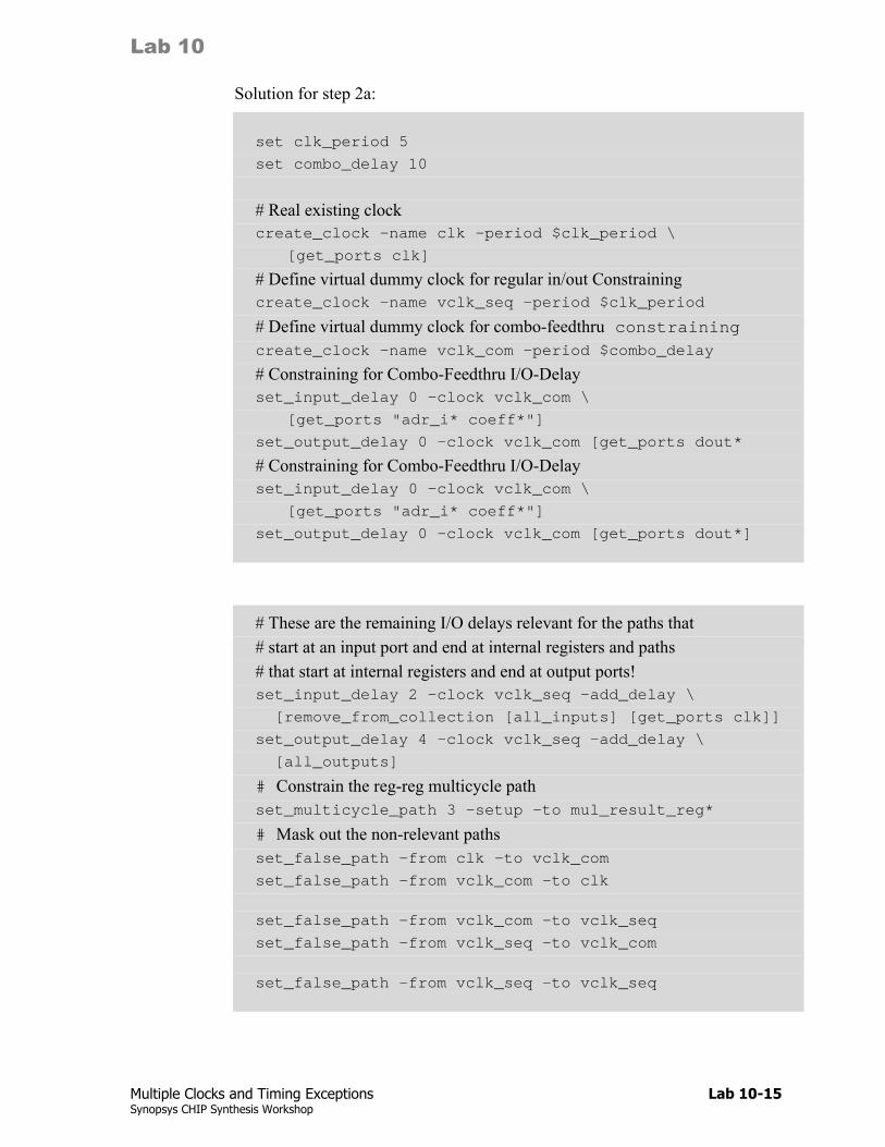
Solution for step 2a:
set clk_period 5
set combo_delay 10
# Real existing clock create_clock -name clk -period $clk_period \
[get_ports clk]
# Define virtual dummy clock for regular in/out Constraining create_clock -name vclk_seq -period $clk_period
# Define virtual dummy clock for combo-feedthru constraining create_clock -name vclk_com -period $combo_delay
# Constraining for Combo-Feedthru I/O-Delay set_input_delay 0 -clock vclk_com \
[get_ports "adr_i* coeff*"]
set_output_delay 0 -clock vclk_com [get_ports dout*
# Constraining for Combo-Feedthru I/O-Delay set_input_delay 0 -clock vclk_com \
[get_ports "adr_i* coeff*"]
set_output_delay 0 -clock vclk_com [get_ports dout*]
# These are the remaining I/O delays relevant for the paths that # start at an input port and end at internal registers and paths # that start at internal registers and end at output ports! set_input_delay 2 -clock vclk_seq -add_delay \
[remove_from_collection [all_inputs] [get_ports clk]]
set_output_delay 4 -clock vclk_seq -add_delay \
[all_outputs]
# Constrain the reg-reg multicycle path set_multicycle_path 3 -setup -to mul_result_reg*
# Mask out the non-relevant paths set_false_path -from clk -to vclk_com
set_false_path -from vclk_com -to clk
set_false_path -from vclk_com -to vclk_seq
set_false_path -from vclk_seq -to vclk_com
set_false_path -from vclk_seq -to vclk_seq
Multiple Clocks and Timing Exceptions Lab 10-15 Synopsys CHIP Synthesis Workshop

Lab 10
Question 14. Do all paths meet setup timing now?
Yes. All setup constraints are met.
Question 15. Where do these hold violations suddenly come from?
When the multicycle exception was applied to move the setup capture edge to the third clock edge, the hold capture-edge moved as well. See your student guide for details.
Question 16. What capture edge is the hold check performed at for “clk”?
10 ns.
Question 17. Are all violations gone now?
Yes. Finally done.
Lab 10-16 Multiple Clocks and Timing Exceptions Synopsys CHIP Synthesis Workshop