workshop on defects in wide band gap semiconductors 2014 prog… · workshop on defects in wide...
TRANSCRIPT

Workshop on Defects in Wide Band Gap Semiconductors
September 23, 2014
University of Maryland, College Park
http://widebandgap.umd.edu

Disclaimer: the views expressed are those of the authors and do not necessarily reflect the views of the National Science Foundation
Workshop Program
7:00 Continental Breakfast and Registration 7:45 – 8:00 Welcome Remarks: Robert Briber, Chair of UMD’s Department of
Materials Science & Engineering 8:00 – 8:30 Workshop Objectives
Systems Requirements – K. Shenai, “Power Switch Considerations” Reliability Requirements – A. Christou, “Wide Bandgap Semiconductor Reliability and Material Defects” Material Requirements – M. Razeghi, “Novel Approaches to Addressing the Challenge of Growing Defect-‐Free Wide Bandgap Semiconductors”
8:30 – 9:30 Plenary Session: Related Programs National Science Foundation – D. Pavlidis, “Defects and Manufacturing in Wide Bandgap Semiconductors” Department of Energy – M. Johnson Office of Naval Research Programs-‐ P. Cho PEIC Perspectives – K. Evans, “The Business of Defects”
9:30 – 10:45 Invited Session 1: Key SiC Material Challenges M. Loboda, Emerging Challenges in Evaluation of Silicon Carbide M. V. S. Chandrasekhar, Defects in 4H-‐SiC epitaxial growth using tetrafluoridesilane as Si precursor J. Narayan, Defects and Interfaces in Thin Film Heterostructures B. Ragothamachar, Defect Origins and Behavior in Wide Band Gap Semiconductors N. Mahadik, Observation of Stacking Faults from BPDs in Buffer Layers and Their Influence on Pulsed Power Devices
10:45 – 11:00 Coffee Break (Poster Session) 11:00 – 12:00 Invited Session 2: Key GaN Material Challenges
S. Mahajan, Origins of Threading Dislocations in GaN Layers Grown on (0001) Sapphire Substrates

2
D. Demchenko, Theoretical and Experimental Identification of Point Defects in GaN G. Imhoff, Processing-‐Related Defects in 4H SiC Devices L. Salamanca-‐Riba, Structural and Chemical Characterization of the Transition Layer at the Interface of NO-‐annealed 4H-‐SiC/SiO2 Metal-‐Oxide-‐Semiconductor Field-‐Effect Transistors
12:00 – 1:00 Rapid Presentation Session J. Cumings, In-‐situ TEM studies: A bright future for wide-‐bandgap semiconductors? M. Leite, Wide Bandgap Materials for Ultra-‐High Efficiency Solar Cells A. Woodworth, Principles of bulk SiC growth by the Large Tapered Crystal growth process M. E. Zvanut, The reduction in the number of Mg acceptors in AlxGa1-‐xN E. Ertekin, Modeling the Excited State of Carbon Vacancy Defect in 4H-‐SiC G. Subramanyam, Nondestructive Assessment of Surface and Subsurface Defects in Wide-‐bandgap Semiconductors using Photon Back Scattering M. Reshchikov, HVPE-‐grown GaN with low concentration of point defects studied by photoluminescence A. Mane, 2D-‐Layered Transition Metal Dichalcogenides Growth by Atomic Layer Deposition for MOS Gate Channel Applications J. Shen, Nanotechnology Enabled Defect Reduction in WBG Materials A. Yanguas-‐Gil, The role of surface kinetics on surface morphology and defect evolution during WBG semiconductor epitaxy A. Davydov, Selective HVPE growth of GaN core/shell pillar arrays on Si substrate M. Sunkara, Self-‐oriented growth of Gallium Nitride on molten Gallium for large single crystals

3
1:00– 2:00 Lunch (Poster Session) 2:00 – 4:00 Invited Session 3: Materials Related Challenges
J. Hite, Reduction and Identification of Extended Defects in GaN K. Jones, Problems with Controlled Doping of GaN Below 1016 cm-‐3 J. Freitas, State of the Art of bulk III-‐nitride substrates and films for device fabrication R. Green, Influence of Near-‐Interfacial Oxide Traps on Stability and Reliability of Commercial SiC MOSFETs J. Weil, Detection and Mitigation of Surface Defects in Transfer-‐Doped Single-‐Crystal Diamond Films S. Pantelidis, Defect-‐mediated degradation of III-‐V HEMTs P. Lenahan, Electrically Detected Magnetic Resonance Observation of Performance Limiting Defects in 4H SiC MOSFETs N. Goldsman, Passivation schemes for hole traps in 4H-‐SiC MOSFETs
4:00 – 4:15 Coffee Break (Poster Session) 4:15 – 5:15 Breakout Sessions
Condensed Matter Physics and Modeling Moderators: N. Goldsman, P. Chung
Materials Synthesis and Characterization Moderators: G. Subramanyan, M. Loboda
Reliability and Packaging Moderator: P. McCluskey
5:15 – 6:00 Breakout Session Presentations – 15 min. each 6:00 – 8:00 Reception & Dinner, with Concluding Remarks from Workshop
Chairs

4

5
Index of Abstracts Christou, Aris Wide Bandgap Semiconductor Reliability and Material
Defects 7
Cumings, John In-‐situ TEM studies: A bright future for wide-‐bandgap semiconductors?
9
Davydov, Albert Selective HVPE growth of GaN core/shell pillar arrays on Si substrate
10
Demchenko, Denis
Theoretical and Experimental Identification of Point Defects in GaN
12
Ertekin, Elif Modeling the Excited State of Carbon Vacancy Defect in 4H-‐SiC
14
Evans, Keith The Business of Defects 16 Freitas, Jaime State of the Art of bulk III-‐nitride substrates and films for
devices fabrication 17
Goldsman, Neil Passivation schemes for hole traps in 4H-‐SiC MOSFETs 18 Green, Ron Influence of Near-‐Interfacial Oxide Traps on Stability and
Reliability of Commercial SiC MOSFETs 20
Hite, Jennifer Reduction and Identification of Extended Defects in GaN 22 Imhoff, Eugene Processing-‐Related Defects in 4H SiC Devices 24 Jones , Ken Problems with Controlled Doping of GaN Below 1016 cm-‐
3 26
Leite, Marina Wide Bandgap Materials for Ultra-‐High Efficiency 28 Lenahan, Pat Electrically Detected Magnetic Resonance Observation of
Performance Limiting Defects in 4H SiC MOSFETs 30
Loboda, Mark Emerging Challenges in Evaluation of Silicon Carbide 32 Mahadik, Nadeem
Observation of Stacking Faults from BPDs in Buffer Layers and Their Influence on Pulsed Power Devices
33
Mahajan, Subhash
Origins of Threading Dislocations in GaN Layers Grown on (0001) Sapphire Substrates
35
Mane, Anil 2D-‐Layered Transition Metal Dichalcogenides Growth by Atomic Layer Deposition for MOS Gate Channel Applications
37

6
Narayan, J. Defects and Interfaces in Thin Film Heterostructures 39 Pantelides, Sokrates
Defect-‐mediated degradation of III-‐V HEMTs 40
Pavlidis, Dimitri Defects and Manufacturing in Wide Bandgap Semiconductors
42
Raghothamachar, Balaji
Defect Origins and Behavior in Wide Band Gap Semiconductors
43
Razeghi, Manijeh Novel Approaches to Addressing the Challenge of Growing Defect-‐Free Wide Bandgap Semiconductors
45
Reshchikov, Michael
HVPE-‐grown GaN with low concentration of point defects studied by photoluminescence
47
Salamanca-‐Riba, Lourdes
Structural and Chemical Characterization of the Transition Layer at the Interface of NO-‐annealed 4H-‐SiC/SiO2 Metal-‐Oxide-‐Semiconductor Field-‐Effect Transistors
49
Shen, John Nanotechnology Enabled Defect Reduction in WBG Materials
51
Shenai, Krishna Power Switch Considerations 53 Subramanyam, Guru
Nondestructive Assessment of Surface and Subsurface Defects in Wide-‐bandgap Semiconductors using Photon Back Scattering
57
Sudarshan, T.S. Defects in 4H-‐SiC epitaxial growth using tetrafluoridesilane as Si precursor
59
Sunkara, Mahendra
Self-‐oriented growth of Gallium Nitride on molten Gallium for large single crystals
61
Weil, James Detection and Mitigation of Surface Defects in Transfer-‐Doped Single-‐Crystal Diamond Films
63
Woodworth, Andrew
Principles of bulk SiC growth by the Large Tapered Crystal growth process
64
Yanguas-‐Gil, Angel
The role of surface kinetics on surface morphology and defect evolution during WBG semiconductor epitaxy
66
Zvanut, Mary Ellen
The reduction in the number of Mg acceptors in AlxGa1-‐xN
68

Wide Bandgap Semiconductor Reliability and Material Defects
Aris Christou
Department of Materials Science and Engineering, University of Maryland, College Park, MD
Contact information: [email protected]; phone 1 301 405-5208; christou.umd.edu
BIOGRAPHY
Professor Christou’s technical contributions encompass the development of materials surface and interface science and methodologies for achieving reliable high frequency devices, power electronic devices and circuits. Professor Christou’s contributions established the critical relationships which exist between materials, materials surfaces and interfaces, process science, and reliability. His developed “Failure Physics” approach to the design and manufacture of compound semiconductor devices and circuits has been critical in achieving low cost-high yield commercial products. He has authored four books and has been the editor of three others. Dr. Christou has more than 200 publications in archival journals and 12 patents, and has organized international conferences in Compound Semiconductor devices, materials and reliability.
TECHNICAL ABSTRACT
The state-of-the-art power switching devices made from SiC and GaN semiconductors contain a high density of crystal defects. Most of these defects are present in starting wafers and some are generated during device processing. There is little conclusive evidence so far on the exact role that the crystal defects paly on device performance, manufacturing yield, and more importantly, long-term field-reliability especially when devices are operating under extreme stressful environments. This paper provides a review of the current state-of-the-art of SiC and GaN power semiconductor material technology, and the potential impact crystal defects may have on high-density power switching electronics. SiC defects include basal plane dislocations (BPDs), threading screw dislocations (TSDs) and threading edge dislocations (TEDs). The detrimental influence of BPDs on device performance is generally acknowledged and much effort has been devoted to the reduction of their density [1]. On the other hand, it is believed that TSDs and TEDs that thread into the epilayers are relatively benign with respect to short-term device performance. However, there is evidence that these latter defects have a significant impact on long-term device reliability [2], however, little is known about the behavior of these defects under high voltage testing. It is therefore of great importance to investigate ways to reduce the impact of these defects on device performance and reliability.
It is well known that III-N materials suffer from both extended and point defects, each of which will challenge the material’s use in energy applications. Extended defects include vertical threading dislocations of both edge and screw type. The latter defects have been shown to be correlated with leakage in vertical two-terminal device structures, while the influence of the former is still undetermined and remains a critical research issue. These extended defects occur in all epitaxial layers grown on c-plane substrates (the predominant and largest area substrate type) and are the result of the lack of a high quality substrate bulk material, as well as substrate surface. Even in the best current substrate technology, low-defect seeds are scarce. Point defects influence the background carrier concentration in low-doped layers and various recombination processes. The nature of III-N materials makes nitrogen-vacancies a predominant point
7

defect that automatically dopes the crystal n-type; but there are impurities (oxygen and carbon) from most growth environments that also contribute to conductivity. These defects are not well understood and not well controlled. Such defects must be minimized so as to realize drift regions that will support both high blocking voltages and low ON-state resistances.
The recent advances of AlGaN/GaN HEMTs grown on Si for addressing the needs of the power electronics market in the 0-900 V range have indicated that GaN on Si may be the most cost effective solution. The main problem with this technology is the large lattice and thermal mismatch between Si and III-nitride layers, which result in several electrically active defects affecting both device performance and reliability. Furukawa Electric initially reported that to increase breakdown voltage it is necessary to compensate the GaN buffer layer by using p-type dopants. Such an approach allowed Furukawa to report a breakdown voltage as high as 525 V with a low specific on resistance. This investigation, using elaborate buffer layer configurations did show the direct relationship between threading dislocation density and breakdown voltage. These results and our present investigations show that to achieve a high breakdown voltage, thick buffer layers and carefully designed structures are required. However the growth of thick buffer layers either by MOCVD or MBE is challenging due to both the thermal mismatch as well as the lattice mismatch. The previous investigations on the reliability physics of GaN have identified strain related traps originating at the GaN/SiC as well as the GaN/Si substrate interface. The presence of mismatch in lattice parameter and coefficient of thermal expansion between GaN on common substrates like Al2O3, SiC, and (111) Si results in a variety of defects that adversely affect device performance. Among the potential defects, threading dislocations (TDs) are the primary defects seen in GaN epitaxial layers. These dislocations can be categorized as pure edge dislocations, pure screw dislocations, or mixed dislocations. Edge dislocations, defined by the Burgers vector 𝑏!"#! =
!!< 1120 >,
run parallel to the basal (c-) plane of the wurtzite GaN structure. Screw dislocations are defined by a Burgers vector 𝑏!"#$% = < 0001 > and run perpendicular to the GaN basal plane/parallel to the c-axis. While dislocations have been observed in all heteroepitaxially grown GaN films, TDs are especially prevalent in GaN on (111) Si substrates. The GaN-(111) Si lattice parameter mismatch (≈17%) and coefficient of thermal expansion mismatch (≈56%) are significantly larger than the mismatch with SiC or Al2O3 substrates, leading to the introduction of greater tensile stresses in the GaN layer during and after growth at elevated temperatures. The lattice strain and thus dislocation density are much higher at the GaN/buffer layer interface than at the upper surface of the GaN film. Due to the merger of screw dislocation as the distance from the substrate/buffer layer increases, increasing film thickness leads to an overall reduction in defect density. In addition, the screw dislocation reduction leads to edge dislocations becoming the dominant defect near the surfaces of GaN films.
REFERENCES [1] Avionics Integrity Program (AVIP), MIL-STD-1796A (USAF), October 13, 2011.
[2] K. Shenai, R. S. Scott and B. J. Baliga, “Optimum semiconductors for high-power electronics,” IEEE Trans. Electron Devices, vol. 36, no. 9, pp. 1811-1823, Sept. 1989.
8

In-situ TEM studies: A bright future for wide-bandgap semiconductors?
John Cumingsa aDepartment of Materials Science and Engineering, University of Maryland, College Park, MD, 20742-2115
Main author’s contact info: [email protected]; phone 1 301 405-0789; http://terpconnect.umd.edu/~cumings/
BIOGRAPHY John Cumings received his BS in 1997 from Boston University and his PhD in 2002 from UC Berkeley. After holding a postdoctoral research position at Stanford University, he joined the faculty of the Department Materials Science and Engineering at the University of Maryland in 2005, and was promoted to Associate Professor in 2012. Cumings has received several awards for his work, including an IBM graduate research fellowship, an NSF CAREER award, and the A. James Clark School of Engineering's Junior Faculty Outstanding Research Award. His research is in the area of nanomaterials and in situ transmission electron microscopy, and he has published more than 50 research articles on the topic.
TECHNICAL ABSTRACT In the past 15 years, there have emerged a large set of home-grown and commercially-available tools for conducting
experiments inside transmission electron microscopes (TEMs), during the application of a growing set of applied stimuli. From the outset, such studies have focused on the ability to apply strain or heat to small structures, while observing for structural changes. Such capabilities have grown to include electric and magnetic fields, gaseous environments, and light illumination conditions, among other stimuli. This presents a fertile area in which one can imagine many possible studies to push the forefront of science and engineering for wide bandgap devices. The simplest of experimental opportunities might focus on the influence of large current densities, which are known to induce a host of structural changes, some of which may alter performance, while others may not. If such studies could be coupled with high-resolution cathodoluminescence studies, it could be determined which defects are giving rise to non-radiative recombination in these devices, as well as the defects for which non-radiative recombination appears to be uninfluenced. Also, electron energy-loss spectroscopy (EELS) may give information about bandgap (from plasmon generation) and photonic density of states (from the low-loss spectrum), both of which my give detailed information about the heterogeneity and light-efficiency of devices. Put together, there are a number of opportunities for future in-situ work in wide-bandgap devices, and my presentation will give some background and lay out some possible paths forward in the near-term.
Keywords: in-situ, TEM, electron microscopy, EELS, cathodoluminscence
9

Selective HVPE growth of GaN core/shell pillar arrays on Si substrateAlbert Davydov1, Sergiy Krylyuk1,2, Ratan Debnath1, Jong-Yoon Ha1,2, Baomei Wen1, Mathew King3 and Abhishek Motayed1,2
1Materials Science and Engineering Division, National Institute of Standards and Technology, Gaithersburg, MD 20878 2Institute for Research in Electronics and Applied Physics, University of Maryland, College Park, MD 20742 3Northrop Grumman ES, Linthicum, MD 21090
Main author’s contact info: [email protected]; phone 1 301 975-4916; http://www.ctcms.nist.gov/~davydov/
BIOGRAPHY Albert Davydov is a Staff Member of the National Institute for Standards and
Technology. He received his Ph.D. in Chemistry from Moscow State University (Russia) in 1989. He was an Assistant Professor of Chemistry at Moscow State University (1989-1993), an Invited Researcher at the University of Sheffield, UK (1992-1993), a Research Scientist at the University of Florida (1993-1997), and a NIST Research Associate at the University of Maryland (1997-2005).
He joined NIST fulltime in 2005 and is now active in the area of semiconductor thin films, nanowires and 2D materials and devices. He is presently a Group Leader of the Functional Nanostructured Materials Group and a Project Leader on “Low-dimensional semiconductors for sensors, optoelectronics and energy applications” at the Materials Science & Engineering Division at Material Metrology Laboratory at NIST.
Dr. Davydov has more than 25+ years of experience and 100+ publications related to growth of bulk crystals, deposition of thin films, and the fabrication, characterization, and processing of a wide range of nanostructured electronic and optical materials. He is also involved in thermodynamic modeling of phase diagrams for metal/semiconductor systems.
He is a Head of the Semiconductor Task Group for the International Centre for Diffraction Data, Co-chair of the Reference Materials Task Group at ASTM Subcommittee on Compound Semiconductors, leader of the review panel for the NSF-NRI program on “Nanoelectronics for 2020 and Beyond”, and an Associate Editor of the Journal of Mining and Metallurgy.
TECHNICAL ABSTRACT GaN-based core-shell nanowires have gained significant attention in recent years due to their potential use in
electronics, optoelectronics, sensing and energy. These structures show significant benefits including large active surface area, reduced density of structural defects, greater carrier confinement, enhanced light extraction etc. This talk discusses design and fabrication of periodic arrays of vertically aligned GaN core/shell micro- and nano-pillar arrays, realized with a combination of top-down etch and Halide Vapor Phase Epitaxy (HVPE) overgrowth.
First, ICP and wet etch of lithographically patterned GaN-on-Si epilayers produced a regular array of n-GaN micro- and nano-scale pillars on the (111) Si substrate (Fig. 1a). Then, the selective HVPE growth was applied to fabricate n- and p-type epitaxial shells over the etched pillars to complete the core/shell design (Fig. 1b). Optimization of both etching and HVPE resulted in reduction of dislocation density in the GaN shells (Fig. 2) aimed at improving transport and optical properties of these device platforms.
Control of faceting in the HVPE-grown shells produced core/shell pillars shaped as a) truncated hexagonal pyramids with the {1101} semi-polar sidewalls, or b) hexagonal prisms with the {1100} non-polar sidewalls. XRD, TEM, PL, CL and Raman scattering measurements revealed improved crystal quality of GaN shells as well as significant strain relaxation.
Strategies toward fabricating 3D GaN-on-Si micro-/nano-structures for large-area LEDs, field emitters, and photodetectors (Fig. 3) will also be discussed.
Keywords: HVPE, dry etch, selective epitaxy, semipolar and non-polar GaN planes
10

Fig. 1 SEM images of core/shell GaN pillars: a) array of n-GaN pillars produced by ICP etching; b) p-type shells grown by HVPE over the n-type pillars (false colors, light-red for n-GaN and light-green for p-GaN, are used for clarity to distinguish between n- and p-type materials.
Fig. 2 Cross-section TEM of an individual core/shell GaN pillar (false colorized for clarity). Dislocation density in the core (red colorized) is significantly higher as compared to nearly dislocation-free shell (green colorized)
Fig. 3 Cross-section SEM of a core/shell/shell p-i-n pillar array
11

Theoretical and Experimental Identification of Point Defects in GaN Denis O. Demchenko and Michael A. Reshchikov
Department of Physics, Virginia Commonwealth University, 701 W Grace St, Richmond, VA, USA 23220
Main author’s contact info: [email protected]; phone 1 804 828-7077
BIOGRAPHY Denis O. Demchenko: received M.S. degree in physics from Odessa State University (Ukraine) in 2006, working on photoluminescence properties of porous silicon. Received Ph.D. degree in Materials Science from South Dakota School of Mines and Technology in 2002, worked on theoretical calculations of spin-dependent transport in semiconductor heterostructures. From 2002 to 2005, postdoctoral fellow at the department of physics at Georgetown University, working on first principles and many-body calculations of magnetic and strongly correlated materials. From 2005 to 2008, postdoctoral fellow at Lawrence Berkeley National Laboratory, work focused on calculations of semiconductor quantum dots and nanowires. In 2008, joined the Department of Physics at Virgina Commonwealth University as an assistant professor.
TECHNICAL ABSTRACT Gallium nitride (GaN) is a promising material for high-power/high-frequency electronics. In particular, thick GaN
layers on sapphire substrates and freestanding GaN, grown by hydride vapor phase epitaxy (HVPE), are expected to have very high breakdown voltage due to a low density of defects in this material. Therefore characterization and control of point defects is crucial for the quality of the material. In many cases point defects in GaN create deep levels in the bandgap, causing numerous photoluminescence (PL) bands of variety of colors and intensities. Nevertheless, in spite of the importance of the defects for the practical applications, majority of the point defects in GaN that are responsible for broad photoluminescence bands remain unidentified.
It has been recently shown that novel hybrid functional calculations yield accurate thermodynamic and optical transition levels created by point defects. This allows direct comparison of experimentally measured PL spectra with calculations of optical properties of defects, thus allowing their identification. Here we demonstrate an example of the identification of the point defects by comparison of the hybrid functional calculations and experimental PL measurements, using a case of yellow luminescence (YL) and green luminescence (GL) in GaN.
In photoluminescence (PL) studies of high-quality freestanding GaN grown by HVPE, the YL band with a maximum at about 2.2 eV and the green luminescence (GL) band with a maximum at about 2.4 eV are the dominant defect-related PL bands.1 Previously, the YL and GL bands were attributed to transitions of electrons from the conduction band to the 2−/− and −/0 transition levels, respectively, of the VGaON complex.2 However, according to recent hybrid density functional calculations, the PL band caused by transitions of electrons from the conduction band to the 2−/− level of VGaON is expected to have a maximum at 1.4 eV; i.e., in the infrared region.3 Moreover, the exponential decay of the GL band at low temperatures was explained with the assumption that the GL band is caused by transitions of electrons from an excited state, located very close to the conduction band minimum (CBM), to the −/0 level of the VGaON acceptor.1 However, such an assumption is not well justified. Indeed, an excited state close to the conduction band is possible for a positively charged deep donor, whereas the VGaON acceptor does not have donor-like excited states. Thus, a revision of the attribution for the GL band in GaN is needed.
Regarding the YL band, two assignments have been recently suggested based on modern first principles calculations. Lyons et al.4 attributed the YL band to the CN defect, whereas Demchenko et al.3 proposed that the YL band is caused by the CNON complex. The CNON complex is a deep donor with the 0/+ level at 0.75 eV above the
12

valence band maximum (VBM). The CN defect in GaN is a deep acceptor with the −/0 level at 0.9-1.1 eV above the VBM. The schematic band diagram including these thermodynamic transition levels is shown in Fig.1.
In addition to the acceptor −/0 level of CN, calculations have predicted the existence of the 0/+ level for this defect at 0.43 eV above the VBM.3 Since the −/0 level of CN and the 0/+ level of CNON have similar energies, it is possible that both the CN and CNON defects produce YL bands with similar shapes and positions (Fig. 1). However, due to the difference in their electronic structure, these defects can be distinguished through the study of the effect of excitation intensity on the PL spectrum. Indeed, it is expected that the CN acceptors in n-type GaN can be saturated with holes (causing saturation of the YL band intensity), and at higher excitation intensities the defects will begin to capture an additional hole. Subsequently, transitions of electrons from the conduction band to the 0/+ level of CN will cause a “secondary” PL band, which peaks at higher photon energies (Fig. 1). In contrast, there is only one optically active transition level for the CNON complex in the bandgap of GaN. A second level, +/2+ is predicted to be very close to the valence band (Fig. 1), and will act as a repulsive center for holes. Therefore the
saturation of the CNON–related YL band will not be followed by the emergence of another PL band at higher photon energies. This important distinction between the two defects should allow reliable attribution of the YL band to either CN or CNON, depending on the existence of the secondary band.
In this work, by combining hybrid functional calculations with experimental measurements of a number of samples, we conclude that the GL band with a maximum at 2.4 eV, is caused by electron transitions via the 0/+ level of the CN defect. The PL bands associated with the CN and CNON defects can both be called YL bands since they have only slightly different positions of their maxima. It appears that in a majority of GaN samples, the CNON complex is responsible for the YL band. The CN defect can be revealed through the observation of the secondary (GL) band only in high-quality GaN grown by HVPE technique. Thus, computed electronic properties of point defects obtained using hybrid functional approach coupled with PL measurements allow reliable identification of defects.
Keywords: GaN, luminescence, point defects
1 M. A. Reshchikov and H. Morkoç, J. Appl. Phys. 97, 061301 (2005). 2 M. A. Reshchikov, H. Morkoç, S. S. Park, and K. Y. Lee, Appl. Phys. Lett. 81, 4970 (2002). 3 D. O. Demchenko, I. C. Diallo, and M. A. Reshchikov, Phys. Rev. Lett. 110, 087404 (2013). 4 J. L. Lyons, A. Janotti, and C. G. Van de Walle, Appl. Phys. Lett. 97, 152108 (2010).
Figure 1. Schematic band diagram with theoretically predicted transition levels for the CNON complex and the isolated CN defect. Calculations show that the CNON complex forms the 0/+ transition level in the bandgap, while CN forms two transition levels: −/0 and 0/+. The CNON complex is expected to generate only the YL band. The CN defect can generate the YL band and an additional, higher energy band after the YL is saturated.
13

Modeling the Excited State of Carbon Vacancy Defect in 4H-SiC Elif Ertekina, Bengt G. Svenssonb, Krishna Shenaic
aDept. of Mechanical Science & Engineering, University of Illinois, Urbana-Champaign, Illinois 61801 (USA); bDept. of Physics/Centre for Material Science & Nanotechnology, University of Oslo, Oslo (Norway); cEnergy Systems Division, Argonne National Laboratory, Argonne, Illinois 60439 (USA)
Main author’s contact info: [email protected]; phone: (217) 333-8175; oasis.mechse.illinois.edu
BIOGRAPHY Elif Ertekin: Elif Ertekin is an Assistant Professor in the Department of Mechanical Science and Engineering at the University of Illinois, Urbana-Champaign, Illinois. She received the BS degree in Mathematics and the BS degree in Engineering Science and Mechanics from The Pennsylvania State University, and a PhD degree in Materials Science and Engineering from The University of California, Berkeley, CA. She was a post-doctoral associate at the Berkeley Nanoscience and Nanotechnology Institute and in the Materials Science Department at the Massachusetts Institute of Technology. Her research interests are focused on computational modeling and simulation for atomic-scale design of materials for sustainable energy generation, conversion, and storage. Her work focuses on understanding the bulk and defect properties of semiconductors for photovoltaics and other applications, via first-principles simulation methods such as the density functional theory and quantum Monte Carlo methods.
TECHNICAL ABSTRACT For the development and commercial deployment of wide band gap (WBG) semiconductor power devices
based on 4H-SiC, one of the most severe shortcomings in need of immediate attention is the influence of point defects that degrade device performance and reliability. In particular, the response of defects to stressful operating conditions such as high-level carrier injection and rapid switching are not well characterized and understood. However, the excited state of point defects probably plays a critical role in performance and reliability degradation. Through extensive experimental characterization, the carbon vacancy, VC, has recently been identified as a dominant ‘killer defect’ in high-voltage 4H-SiC bipolar mode power devices. In this program, we will carry out a ground-up analysis of VC, (i) starting from a quantum mechanical assessment of the defect formation energy, thermal and optical ionization energies, (ii) extending to an atomistic description of the defect interaction with extended lattice defects, and (iii) ultimately realizing a predictive model to describe the excited state of the defect under conditions of high carrier injection, high voltage switching rate, and high temperature.
Carbon Vacancy as a Killer Defect: The substrate manufacturing process for 4H-SiC relies on high-temperature CVD which leads to enormous thermal stress and a high defect density. These defects include but are not limited to point defects such as the VC, threading screw dislocations, threading edge dislocations, and stacking faults. As characterized by available avalanche energy measurements, dv/dt experiments, etc. [1], these defects and their interactions play a key, but not well-characterized role, in the performance degradation and long-term reliability of practical devices. For example, these crystal defects introduce localized potentials in the semiconductor crystal lattice that can strongly distort the electronic band structure. However, detailed understanding of the excited state of these defects is currently lacking. Detailed DLTS measurements reveal the presence of VC, its persistence to annealing [2] (Fig. 1a), and its effect on minority carrier lifetime [3].
14

Calculated)defect)thermal)ioniza2on)levels)(DFT)vs.)QMC))
Nega2vely)Charged)N)Neutral)N)
QMC)LDA)
1)
2)
Form
a2on
)Ene
rgy)(eV))
(a))Persistence)of)VC)(Z1/2))in)SiC)to)annealing) (b))QMC)Descrip2on)of)NO)in)wurtzite)ZnO)
Fig. 1: (a) DLTS Measurements of (b) Comparison of defect properties of N in wide band gap semiconductor (ZnO) calculated from conventional density functional theory and quantum Monte Carlo.
Defect Properties via Quantum Monte Carlo Methods: DLTS experiments under optical excitation show that each VC can capture and trap two electrons (and in fact that it is a negative U center) [4]. Correspondence between photo-EPR and DLTS measurements have been used to identify the different charged states of the defect. The first goal of this work is to carry out high-accuracy simulation via quantum Monte Carlo methods, to validate the excited state spectral assignments, the thermal ionization energies, and the negative-U behavior. Quantum Monte Carlo methods are a suite of stochastic tools for the direct solution of the many-particle interacting Schrodinger equation. Because of their direct, parameter-free treatment of electron correlation, they have been shown to offer unprecedented and benchmarking accuracy on several defect properties to date [5] (Fig. 1b).
Interaction of VC with Extended Defects of Interest and Under Realistic Operating Conditions: In the second phase of this work, the influence of VC on electronic properties under realistic operating conditions will be determined. Atomistic physics models can give insights into the interaction between charged states of VC and extended defects that are present in WBG semiconductors, such as threading screw dislocations (TSDs) and threading edge dislocations (TEDs). The build-up of charged/excited state of VC at dislocations and grain boundaries can result in localized charging. Two particularly relevant reliability parameters are avalanche and dv/dt capabilities of high-voltage power devices. The carrier trapping behavior of VC emerging from the quantum mechanical models can be extended to conditions of high voltage switching (high dv/dt). Under high voltage switching, the injection of space charge induces the defect to possibly act as a charge generation center, resulting in the formation of a microplasma (and ultimately device failure). Additionally the response of defects to high currents and/or voltages that result in charging may explain observed reduction in avalanche energy, especially at high chip temperatures.
1. K. Shenai, M. Dudley and R. F. Davis, “Rugged electrical power switching in semiconductors – asystems approach,” Proceedings of the IEEE, vol. 102, no. 1, pp. 35-52, Jan. 2014
2. Alfieri et al., J. Appl. Phys. 98, 043518 (2005)
3. Danno et al., Appl. Phys. Lett. 90, 202109 (2007); Kimoto et al, Mat. Sci. For. 645-658 (2010)
4. Son et al., Phys. Rev. Lett. 109 187603 (2012)
5. E. Ertekin et al, Phys Rev. Lett. (2012) .; E. Ertekin et al., Phys. Rev. B. (2013).
Keywords: Silicon carbide, point defect, carbon vacancy, excited state, high carrier injection, high voltage switching, avalanche energy, performance, reliability.
15

The Business of Defects Keith R. Evansa,b
aUS Power Electronics Industry Collaborative (PEIC), 300 N. Bridge St., Grand Ledge, MI, USA bKyma Technologies, Inc., 8829 Midway West Road, Raleigh, NC, USA
Contact info: [email protected]; [email protected]; 1 919 789-8880; www.peic-us.org; www.kymatech.com
BIOGRAPHY Keith R. Evans: After receiving a PhD in physical chemistry from Purdue University, Keith became a research scientist at the US Air Force Research Laboratory (AFRL) where he advanced the technology of molecular beam epitaxy for defense applications. He went on to hold executive positions at Semiconductor Laser International, QED/IQE, Veeco Instruments, and Crystal IS, and in 2005 he took on the role of President & CEO of Kyma Technologies. Keith is a member of the American Association for the Advancement of Science (AAAS) and was recently selected to be the new President of the US Power Electronics Industry Collaborative (PEIC).
TECHNICAL ABSTRACT Many scientists love defects. Defects are the subject of thousands of research papers, dissertations, books, and even
entire workshops (like this one) and conferences. A Google Scholar search for articles (not including citations or patents) with “defect or defects” and “semiconductor” anywhere in the article returns 1,260,000 articles for all time and 18,900 since 2013.
Of course, not everyone loves defects. When I was working for the US Air Force Research Laboratory (AFRL) at Wright Patterson Air Force Base our group was focused on developing next generation crystalline III-V heterostructures by molecular beam epitaxy for high performance device applications. We didn’t like to think about defects; rather we liked to focus on chemical and structural perfection. I remember how confused I felt when our materials characterization partners seemed to delight in finding defects in our crystals when I was hoping we would be commended on their perfection. Of course, as I matured I came to realize that their ability to find and understand defects was critical to our figuring out how to reduce and potentially eliminate those defects. We were really on the same team after all!
Today wide bandgap semiconductor (WBGS) materials oriented businesses think of defects not only as technical challenges and opportunities to progress in the continuous pursuit of crystalline perfection, but also as major business opportunities. Defects in semiconductor materials impact the cost, yield, throughput, performance and reliability of semiconductor devices, which, in turn, affect the cost, performance, and reliability of the components and systems they are used in. And because semiconductor materials are used at the very beginning of the device and component manufacturing processes, the impact of defects in those materials are naturally magnified in their impact on component and system cost and performance.
An important question in semiconductor component and systems supply chain analysis is: “What are the ramifications of a particular region or nation that might establish a significant competitive advantage in the manufacturing technology for a particular semiconductor materials system?” Another interesting question is: “What happens if a device doesn’t really benefit from certain reduced defects but materials with such reduced defects are made available in the supply chain?”
This talk will attempt to show the connection between basic R&D in defects in WBGS materials and related supply chain dynamics and business opportunities of a global nature. It will conclude with proposed R&D investment policies and workforce development ideas that are designed to significantly benefit our nation’s potential for significant and long term participation in critical new high technology industries and jobs.
Keywords: Defects, semiconductors, power electronics, wide bandgap, R&D investment, workforce development
16

State of the Art of bulk III-nitride substrates and films for devices fabrication
Jaime A. Freitas, Jr.
Naval Research Laboratory, Washington DC 20375 US [email protected]; phone 202-404-4536
BIOGRAPHY
Jaime A. Freitas, Jr.: received his MSc. and PhD. degrees from the State University of Campinas (São Paulo, Brazil) in condensed matter. He was an Associate Professor of Physics in Brazil, before coming to the Naval Research Laboratory as a visiting scientist in 1982. Presently, he is a Research Scientist at Naval Research Laboratory. Dr. Freitas has more than 200 publications on transport, optical, magnetic, and other physical properties of bulk materials and thin films. He has given more than 90 invited talks at professional meetings, leading universities, and research institutions. Over the last 25 years Dr. Freitas’ work has centered on wide-bandgap semiconductors with emphasis on SiC, diamond, III-V nitrides, and oxides. Dr. Freitas’ current research interests include the use of a combination of defect-sensitive techniques to understand the mechanisms associated with the incorporation of point and extended defects and their role on the material properties, and on the incorporation and activation of impurities and doping species in thin films and bulk materials.
TECHNICAL ABSTRACT
The III-V nitride semiconductor material system continues to play a significant and growing role in a wide range of device technologies. The achievable low intrinsic carrier density of this material system, leading to low leakage and low dark current, place it as one of the most promising material systems for the fabrication of photodetectors and high-temperature electronic devices, in addition to high efficient light emission devices spanning from near IR to deep UV. Despite improved performance of devices fabricated on films deposited on foreign substrates, the properties of thin heteroepitaxial nitride films are still seriously limiting the performance of devices demanding higher material yields. The high growth temperature required to produce these wide bandgap materials exacerbates fundamental material problems such as residual stress, difference in thermal expansion coefficient, low energy defect formation and impurity incorporation. In addition, doping activation and self-compensation are difficult to control at the typically high deposition temperatures. Furthermore, the high concentration of dislocations, resulting mostly from lattice constant mismatch, typically on the order of 109 to 1010 cm-2, must be reduced to improve device performance. Overcoming these limitations will require the use of native substrates to grow electronic grade homoepitaxial films. AlN substrates grown by physical vapor transport and sublimation-recondensation processes are insulators, while GaN grown by hydride vapor phase epitaxy or by ammonothermal processes are always n-type conductive with a free carrier concentration typically between 1017 to 1019 electrons/cm3. High quality epitaxial films with controlled electrical transport properties have been deposited on both substrates by chemical vapor deposition and molecular been epitaxy. The properties of the state of the art of bulk and thick-freestanding film (quasi-bulk) nitride substrates and homoepitaxial films will be reviewed. Bulk InN growth has not been accomplished yet. However, thin and thick films have been deposited in a number of non-native substrates by various techniques. These films are characterized by a high concentration of free carriers and high dislocation densities. In addition, they usually have high concentration of free electrons at the surface. These properties result in poor control of the material electrical properties, which prevents the realization of a number of potential devices. Recently, it has been demonstrated that InN films with good optical properties can also be deposited by ion beam assisted technique.
Keywords: AlN, GaN, InN, HVPE, ammonothermal, structural defects, impurities, self-compensation.
17

Passivation schemes for hole traps in 4H-SiC MOSFETs
N. Goldsmana, D. P. Ettisserrya, A. Akturka, A. Lelisb
aDepartment of Electrical and Computer Engineering, University of Maryland, College Park, MD 20742; bU.S. Army Research Laboratory, Powder Mill Road, Adelphi, MD 20783
Main author’s contact info: [email protected]; phone 240-432-6535;
BIOGRAPHY Neil Goldsman is a professor in the Electrical and Computer Engineering Department at the University of Maryland at College Park where he directs Wide Bandgap Semiconductor Group and the Semiconductor Simulation Laboratory. His recent work has focused on high temperature electronics, UV detectors and semiconductor modeling. He has served as both the conference chair and the symposium chair of the International Semiconductor Device Research Symposium. For the International Conference on Simulation of Semiconductor Processes and Devices, Dr. Goldsman has served as the program chair, and regularly serves on the technical committee. His research has been sponsored by leading governmental and industrial organizations. Dr. Goldsman is the co-recipient of the IEEE Dasher Award; the NSF Research Initiation Award; the University of Maryland’s George Corcoran, Invention the Year, and Business Plan Awards; and Cornell University’s Post Foundation Scholarship. Goldsman has published more than two hundred peer-reviewed technical papers, and supervised the design of over fifty integrated circuits. He has authored two departmental educational texts in electronics. Dr. Goldsman received his Ph.D from Cornell University with a major in Electrical Engineering and a minor in Applied Physics.
TECHNICAL ABSTRACT In this work, we identify single carbon interstitials in the oxide side of 4H-SiC MOSFETs as possible border hole traps, in addition to the traditional oxygen vacancies (E’ centers). We then report on the passivation process of this defect in Nitric Oxide (NO), Hydrogen and Fluorine environments using density functional theory (DFT)-based molecular dynamics and formation energy calculations. Our results suggest that Fluorine and NO passivation could potentially passivate these carbon-related hole traps.
Bias and temperature-induced threshold voltage instability in 4H-SiC MOSFETs remains a serious reliability concern [1]. In Si/SiO2 system, this phenomenon is traditionally attributed to border hole trapping by oxygen vacancies (E’-centers) in the oxide [2]. However, due to the more complex oxidation process of 4H-SiC and the involvement of carbon, additional defects should be probed for potential hole trapping. This motivated us to study the hole trapping properties of the most basic oxide defect involving carbon – an interstitial.
The most stable state of a single carbon interstitial in SiO2 was identified as the carboxyl configuration. The atomic configuration of the carboxyl defect in its neutral state is given in Figure 1(a). The calculated Electron Localization Function (ELF), when compared with the conventional Lewis bond diagram, indicated a carbon-oxygen double bond (based on two lone pairs on the oxygen). The formation energies of the defect in various charge states - ±2, ±1 and neutral - were calculated as a function of Fermi level using DFT [3]. This revealed a +2 to neutral charge transition level (CTL) within the band gap of 4H-SiC (Figure 1(b)). The ELF of the carboxyl defect in its +2 state, given in Figure 1(a), shows back-bonding of positive Si atom with lattice oxygen, very similar to the E’ center hole traps [4]. However, carboxyl defects are further stabilized upon double hole capture by an increase in the bond order between carbon and oxygen (based on the single lone pair on the carboxyl oxygen). These observations lead us to propose carboxyl defects as potential hole traps responsible for NBTI in 4H-SiC MOSFETs, similar to the oxygen vacancy defects.
We then investigated the passivation of the carboxyl defect under different chemical environments using DFT-based molecular dynamics simulations. Firstly, the treatment of the carboxyl defect with Hydrogen modifies the defect structure (Figure 2(a)). For the neutral state of H2-treated carboxyl defect, ELF analysis indicates carbon-oxygen single bond. The formation energy analysis, given in Figure 2(b), suggests the continued existence of +2 to 0 CTL in the lower part of 4H-SiC bandgap. Thus, H2 passivation is unlikely to mitigate hole trapping and ensuing BTI degradation. The
18

stability-providing mechanisms in H2-trated carboxyl defect upon hole capture are very similar to that in carboxyl defect. They include the back-bonding of positive Si atom with network oxygen and the bond order increase between carbon and oxygen (from one to two, as suggested by the single lone pair on carboxyl oxygen).
The passivation of carboxyl defect in NO environment is seen to eliminate the carbon defect through isocyanate (NCO) formation. Two mechanisms were observed, as depicted in Figure (3). Thus, NO treatment could potentially mitigate BTI instability. However, the presence of excess NO molecules was seen to simultaneously incorporate nitrogen into the SiO2 lattice. Such addition of Nitrogen has been previously reported to introduce hole traps leading to Vth instability [5]. Based on these observations, we propose controlled NO passivation with less excess NO molecules for optimum results. This might include repeated short-duration, dilute, NO passivation followed by annealing.
Interestingly, treatment with Fluorine was observed to remove CO from the carboxyl defect in our molecular dynamics simulations. This is expected due to very high Si-F bond energy. The resulting configuration, depicted in Figure 4(a), shows F atoms bonded to two Si atoms. Additionally, Fluorine was also seen to passivate oxygen vacancies in the similar manner [6]. The DFT-based formation energy analysis of the passivated structure indicated no Fluorine-related CTL in the 4H-SiC band gap (Figure 4(b)). Thus, we conclude that Fluorine implantation in 4H-SiC MOSFETs could result in substantial mitigation of Vth instability and enhancement of reliability. However, the effect of reduced dielectric constant of F-doped SiO2, reported previously for Si/SiO2 system [7], on 4H-SiC device performance needs further investigations.
In summary, we identified single carbon interstitials in the carboxyl configuration as potential hole traps in 4H-SiC MOSFETs. A study of their structural transformations upon hole capture revealed significant similarity with the well-known oxygen vacancy hole traps. Fluorine and NO, unlike Hydrogen, are capable of passivating the carboxyl defect. We discussed processing schemes for effective passivation of carboxyl defects using NO and F and related issues.
Keywords: 4H-SiC MOSFET, passivation, hole trap, bias-temperature instability, oxygen vacancy, carbon interstitial, density functional theory, molecular dynamics
REFERENCES: [1] A. J. Lelis et. al., IEEE TED, Vol. 55, No. 8, pp. 1835 (2008). [5] J. Rozen et. al., JAP 103, 124513 (2008). [2] T. Grasser et. al., IEEE TED, Vol. 58, No. 11, pp. 3652 (2011). [6] Y. Ono et. al., APL 62, 375 (1993). [3] D.P. Ettisserry et. al., JAP 115, 103706 (2014). [7] S.M. Han et. al., JAP 83, No. 4, 2172 (1998). [4] T. Uchino et. al., PRB 74, 125203 (2006).
Figure 4: (a) Resulting atomic structure post Fluorine passivation carboxyl defect, (b) formation energy of the structure with neutral state as the reference. No charge transition level is observed in 4H-SiC bandgap.
Figure 2: (a) Atomic structure, electron localization function and structural transformation upon double hole capture in H2-treated carboxyl defect, (b) formation energy of H2-treated carboxyl defect with neutral state as the reference. A (+2/0) CTL is seen at Ev+1.1 eV in 4H-SiC bandgap.
Figure 1: (a) Atomic structure, electron localization function and structural transformation upon double hole capture in carboxyl defect, (b) formation energy of carboxyl defect with neutral state as the reference. A (+2/0) charge transition level (CTL) is seen at Ev+1.4 eV in 4H-SiC gap. (LP=lone pair)
Figure 3: Mechanism of NO passivation of carboxyl defect, indicating defect repair and N incorporation.
19

Influence of Near-Interfacial Oxide Defects on the Stability and Reliability of Commercial SiC MOSFETs
R. Greena, A. J. Lelisa, D. Habersata, M. Ela
aU.S. Army Research Laboratory, 2800 Powder Mill Road, Adelphi, MD, USA 20783;
[email protected]; phone 301-394-5431
BIOGRAPHY Ronald Green: Dr. Green j o i n e d the Army Research Laboratory (ARL) in Adelphi, Maryland in 2005 and received his doctorate degree in electrical engineering in 2010 from Morgan State University in Baltimore, Maryland. His research in the Power Components Branch of the Sensors and Electron Devices Directorate (SEDD) has focused both on developing improved test methods suitable for SiC power MOSFETs and better understanding the key physical mechanisms limiting device performance and reliability. Dr. Green has authored or co-authored many papers related to SiC device research and his primary interests are in the areas of high-power and high-temperature characterization and reliability testing of wide band gap semiconductor devices, and in the development of suitable reliability test standards for military, space, and industrial end-users. Previously, Dr. Green worked in industry, first with Motorola Corporation in Phoenix, Arizona as a manufacturing engineer, establishing a standardized equipment integration approach for scrap reduction in key fabrication areas across many tool sets throughout the semiconductor division. Later, he worked as a process engineer for ON Semiconductor, a spin-off from a division of Motorola Corporation. During this period, Dr. Green worked first in Guadalajara, Mexico, as part of a team working to start up a new 150-mm wafer factory to produce rectifier components. His second assignment took him to Roznov, Czech Republic as part of a team that successfully transferred key device technologies from a factory in Toulouse, France into the Roznov facility.
Technical Abstract
Silicon carbide (SiC) power MOSFETs have been commercially released with the expectation of delivering enhanced performance, reliability, and efficiency in power converter applications. For the SiC industry, development of a high-quality gate-oxide interface continues to be a challenging problem. Nonetheless, commercial SiC MOSFETs have extremely low conduction and switching losses in spite of the low inversion channel mobility and high interface-trap density. However, the activation and charging of intrinsic defects formed during thermal oxidation of SiC may have serious device stability and reliability implications during normal operation. With their emergence into the market place, the development of appropriate testing standards apart from the existing silicon-based ones may be necessary to ensure the reliability of SiC devices. SiC MOSFETs are especially vulnerable to negative bias temperature (NBT) stress-induced shifts of key device parameters. The threshold voltage (VT) exhibits a gate-bias-induced instability even at room temperature [1]. Charging of near-interfacial oxide defects is the likely cause of this experimentally observed phenomenon, where a positive gate-bias stress shifts VT positive, and a negative gate-bias stress shifts VT negative. This effect is enhanced in vintage devices above 100 °C [2], and in more recent devices the onset of VT degradation occurs a decade or more later in time. One possible mechanism dominating the observed high temperature VT response likely involves the activation of precursor oxygen vacancy defects. Recent electrically-detected magnetic resonance (EDMR) studies of thermal oxides on SiC by Cochrane et al.,[3] reveal an EDMR spectrum consistent with an E´-like defect—similar to what was previously identified as a hole trap in the gate oxide of irradiated Si MOS devices [4]. A more recent study shows an increase in the EDMR response with increasing temperature for a constant negative gate-bias stress [5]. EDMR and BTS results independently show that the likely mechanism dominating the high-temperature response of state-of-the-art SiC power MOSFETs involves the activation of additional oxide defects.
Figure 1 is a schematic of the test sequence used to evaluate packaged (TO-247) SiC power MOSFETs. A negative gate-bias stress is periodically interrupted on a logarithmic time scale to make ID-VGS measurements using Agilent
20

Source Measurement Units (SMUs). The threshold voltages plotted in Fig.(s) 2 and 3 are determined from the subthreshold and linear regions of the I-V characteristics using standard extraction techniques for Vinv and VT, respectively. We evaluate oxide trap activation by calculating a ΔVinv from the post-NBT stress and positive bias temperature stress (PBTS) measurements (see Fig.1). This threshold voltage hysteresis (ΔVinv) provides an estimate of the number of switching oxide traps that change charge state under the influence of a gate-bias stress. The degradation of the threshold voltage parameter can be quantified as an excessive shift in Vinv or VT from its pre-stress value. Figure 2 plots ΔVinv for three separate devices as a function of stress time at 125 °C, 150 °C, and 200 °C using the procedure described above. The response is non-linear in log-time and is strongly dependent on stress temperature for a given gate-bias magnitude. For stress times beyond 103 s ΔVinv is larger at 150 °C in comparison to 125 °C. The response at 200 °Cshows a significant increase and acceleration of ΔVinv even at shorter stress times. These results are consistent with an increase in the number of switching oxide traps. Figure 3 plots the change in VT (post- and pre-NBT stress) for two different devices during NBT stress (VGS = –10 V and –15 V) at 125 °C. An insignificant shift in VT occurs at –10 V for stress times out to 106 s. For a stress bias of –15 V, VT accelerates from 0.25 V at 104 s to over 1.5 V by mid-105 s. Thisparticular result demonstrates the effect of bias-stress magnitude on VT stability. In a similar manner, device reliability can also be impacted when Vinv shifts are large enough to cause excessive drain leakage current during off-state operation. This research focuses on developing a better understanding of oxide-trap charging and activation mechanisms that can limit the high-temperature performance and reliability of commercial SiC power MOSFETs.
Keywords: SiC, MOSFET, Reliability, Oxide Traps, Defects, VT Instability References: [1] A. Lelis et al., IEEE Trans. Elec. Dev., Vol. 55(8), p. 1835, 2008 [2] R. Green et al., Mater. Sci. Forum, Vol. 740-742, p. 549, 2013 [3] C. Cochrane et al., J. Appl. Phys., Vol. 109, p. 014506, 2011 [4] P. Lenahan et al., J. Appl. Phys., Vol 55, p. 3495, 1984 [5] P. Lenahan et al., 8th Annual SiC MOS WS, 2013
0.0
0.5
1.0
1.5
2.0
1.E+02 1.E+03 1.E+04 1.E+05 1.E+06
V T S
hift
(V)
Cumulative Stress Time (s)
VGS = -15 V
VGS = -10 V
125 C
0.0
1.0
2.0
3.0
4.0
5.0
6.0
1.E+02 1.E+03 1.E+04 1.E+05 1.E+06
ΔV i
nv(V
)
Cumulative Stress Time (s)
200 C
150 C
125 C
VGS = -15 V
Fig. 2. Shows the temperature dependent change of the threshold voltage as a function of cumulative stress time for three commercial SiC MOSFETs. ΔVinv is calculated as the change in Vinv post-NBT stress and after a 100-s positive gate-stress. Vinv = VGS at ID = 310-5 A.
HT
– VGS (t)
+ VGS
- VGS
100 s
100 s
Time (s)
V GS
(V)
upinvdowninvinvVVV
Fig. 1. Schematic representation of a combined unipolar (NBT stress) and switched-bias stress-and-measure sequence used to monitor parametric degradation and characterize oxide trap activation.
Fig. 3. Gate-bias dependence of the change in VT versus cumulative stress time during NBT stress at 125 °C. The shift in VT is determined by analysis of the pre- and post-NBT stress I-V characteristics.
21

Reduction and Identification of Extended Defects in GaN Jennifer K. Hite
U.S. Naval Research Laboratory, 4555 Overlook Ave, SW, Washington, DC USA 20375
Main author’s contact info: [email protected]; phone 1 202 404-8712
BIOGRAPHY Dr. Jennifer Hite is currently a civilian staff scientist at the U.S. Naval Research Laboratory. Her research interests are in the growth and characterization of III-V semiconductor materials, with a focus on novel growth of gallium nitride structures. Jennifer earned her B.S. in from the University of Florida in Chemical Engineering in 2000. She held an engineering position at Lucent Technologies from 2000 through 2001, after which she returned to the University of Florida to earn her M.S. and Ph.D. in Materials Science and Engineering in 2003 and 2006, respectively. Dr. Hite was the recipient of a Karles Fellowship while at the U.S. Naval Research Laboratory. She has authored or co-authored over 90 papers, patents, and journal proceedings, as well as 130 presentations (including 40 invited).
TECHNICAL ABSTRACT III-N materials continue to play a significant role in a range of technologies from rf electronics to visible and UV
emitters and detectors. This is true despite a heavy population of extended defects in the active regions of these devices, which degrade the operation, potential performance, and reliability of such devices. The large dislocation density observed in GaN films (108-1010 cm-2) arises from growth on non-native, non-latice matched substrates, of which sapphire and SiC are the most common. This talk will focus on advances in two paths to reduce the impact of dislocation density in GaN: growth methods to reduce the initiation and growth of dislocations and techniques to reliably, rapidly, and non-destructively determine spatially defect density are necessary to determine the effects of these defects on device performance.
In order to reduce extended defects in GaN, two different growth methods will be discussed: confined epitaxy (CE) and the use of step-free SiC surfaces. In the CE approach, a substrate, either bare or coated with a continuous GaN film, is patterned with a dielectric mask that has an array of hexagonal openings. Proper growth conditions are then employed to grow vertically up out of the openings and to inhibit lateral growth (such as that required for lateral epitaxial overgrowth approaches). Our efforts have resulted in selectively grown, c-axis oriented materials with atomically smooth surfaces, an order of magnitude reduction in total extended defect densities, and a 50% relaxation of strain – presumably through the presence of free surfaces (Fig. 1). Simple vertical devices (pn homo- and hetero-junctions) have been fabricated with these structures and have demonstrated very low reverse leakage currents. Modeling and experimental efforts show that reducing the size of the openings can lead to even further improvements in material quality [1,2]. Applications of such structures to the development of 2-color UV imaging arrays will be presented. Applications of the approach to non-polar orientations of GaN will also be presented.
The second growth approach that will be discussed is the use of step-free SiC surfaces in the heteroepitaxy of III-N layers. In this approach, a commercial on-axis SiC substrate is patterned into an array of mesas of various sizes and then subject to pure step-flow SiC homoepitaxy. In this technique, developed by Powell et al. [3], any SiC mesa that does not contain a threading substrate screw dislocation can be grown to have an atomically flat top surface completely free of atomic steps by growing all pre-existing SiC mesa surface steps to the mesa edge. These engineered SiC mesa substrates are then used for growth of GaN heteroepitaxial films in a conventional manner employing AlN nucleation layers. Using this approach we have seen an extraordinary reduction in the extended defect density of III-N layers throughout their thickness. Levels <107 cm-2 have been observed via atomic force microscopy (AFM) (Fig. 2a) in 2 μm thick layers (levels comparable to 300 μm thick free standing substrates from HVPE [4]). TEM and modeling efforts have made some progress in understanding why steps have such a significant influence on the formation of vertical threading dislocations in heteroepitaxial III-N layers on SiC and will be briefly discussed [5]. Simple pn diodes have been grown
22

on these step-free mesas and characterized for their electroluminescence (EL) efficiency (Fig. 2b). An average 50% improvement in efficiency was measured for devices on step-free mesas compared to an adjacent stepped mesa. This performance enhancement was realized before optimized processing of these unique structures was complete.
The most precise characterization tool to determine defect density has been transmission electron microscopy, but this is a destructive technique, as are other methods such as molten KOH or photo-electrochemical etching of the surface to reveal dislocation sites. Cathodoluminescence imaging only detects dislocations which change the optical emission of the material. X-ray diffraction can be used to extrapolate dislocation density, but not identify individual defects. In order to understand the impact of dislocations on devices, rapid, non-destructive, spatially oriented techniques are necessary. To address this, electron channeling contrast imaging (ECCI), a non-destructive technique that has been used to examine defects in metals and ceramics, has recently seen use in III-nitride semiconductors. This technique allows for direct imaging of dislocations, grain boundaries, and topological information all at once (Fig. 3). We will present an overview of the uses of ECCI in characterizing III-N materials, culminating in recent work applying the technique to AlGaN/GaN HEMT structures. By imaging the active areas of van der Pauw structures on a single sample with varying mobility, we find a direct negative correlation between screw dislocation and electron mobility.
Keywords: GaN, dislocations, growth, characterization, electron channeling contrast imaging
References: [1] M.E. Twigg, N.D. Bassim, C.R. Eddy, Jr., R.L. Henry, R.T. Holm and M.A. Mastro, MRS Symp. Proc. 831, 677 (2005). [2] J.K. Hite, M.A. Mastro, and C.R. Eddy, Jr., J. Cryst. Growth 312, 3143 (2010). [3] J. A. Powell, P. G. Neudeck, A. J. Trunek, G. M. Beheim, L. G. Matus, R. W. Hoffman, Jr., and L. J. Keys, Appl. Phys. Lett. 77, 1449 (2000). [4] C. Lee, H.Y. Lee, H. Shin, C. Kim, H. Ko, J. Han, H. Kim and K. Lee, Phys. Stat. Sol. C 2, 2137 (2005). [5] M.E. Twigg, N.D. Bassim, M.A. Mastro, C.R. Eddy, Jr., R.L. Henry, J.C. Culbertson, R.T. Holm, P.G. Neudeck, J.A. Powell, and A.J. Trunek, J. Appl. Phys 101, 053509 (2007).
Figure 1. SEM micrograph of CE material (left, feature is 10 μm across), micro-Raman showing reduction in strain of CE material (right).
Figure 2. a) AFM of GaN surface grown on step-free SiC showing low extended defect density, b) image of EL from GaN pn diode grown on step-free SiC.
Figure 3. Example ECCI of MOCVD-grown GaN on sapphire. Examples of threading screw/mixed dislocations are indicated by boxes, those of threading edge dislocations are circled, and a dotted line indicates examples of grain boundaries.
23

Processing-Related Defects in 4H SiC Devices Eugene A. Imhoff1, Karl D. Hobart1, R. E. Stahlbush1, N. A. Mahadik1,
Q. J. Zhang2, A. A. Burk2, B. A. Hull2, J. Young2
1Naval Research Laboratory, 4555 Overlook Ave. SW, Washington, DC 20375, USA 2Cree, Inc. 4600 Silicon Dr., Durham, NC 27703, USA
Main author’s contact info: [email protected]; phone 1 202-404-6211
BIOGRAPHY Eugene Imhoff is a research physicist with the Power Electronics Branch of the U.S. Naval Research Laboratory in Washington, DC. His career since a Ph.D. from Cornell has focused on the properties, processing, and application of compound semiconductors - for two decades in InP and GaAs optoelectronics telecommunications industry and more recently in SiC and GaN power devices for the Navy. He has authored or co-authored more than 100 publications, presentations, and patents.
TECHNICAL ABSTRACT For power electronic devices, 4H silicon carbide (SiC) is nearly an ideal material. The wide bandgap (3.2 eV) gives 4H SiC a high critical electric field (~2 MV/cm) that is over ten times higher than that of Si and, like silicon, SiC devices can be fabricated by planar processing techniques such as ion implantation which result excellent control of critical dimensions. This has lead to high cell densities and high-yield device fabrication processes that can produce large die areas with large current capacity. Another similarity to Si is the indirect nature of the bandgap of SiC which allows for efficient bipolar conduction due to conductivity modulation in devices such as PiN diodes and gate turn-off thyristors.
One of the main challenges in the development of high voltage SiC power devices has been the understanding and management of critical or ‘killer’ defects, i.e., defects that result in infant or random device failure. Such defects can originate in the substrate (e.g., micropipes, polytype inclusions) or in the epitaxial layers (e.g., in-grown stacking faults, carrot defects, triangle defects, etc.) Different defects impact devices in different ways such as the 1c threading screw dislocation which increases off-state leakage in very high voltage devices. A remaining critical defect is the basal plane dislocation (BPD) which, when exposed to a high-density electron-hole plasma, produces a stacking fault. Stacking faults typically affect bipolar devices, causing an increase in the forward voltage drop over time due to a reduction of carrier lifetime and creation of potential barriers. In unipolar devices such as MOSFETs, it has also been shown that the on-state resistance can be degraded when the body diode is allowed to conduct. In this case the stacking fault produces a potential barrier to electrons and the conduction properties are degraded.
Ultraviolent photoluminescence (UVPL) imaging has been instrumental in quantifying the density and origin of these defects. With much concentrated effort over many years, there has been dramatic improvement in both substrates and epitaxially grown layers. Defects levels of all kinds have dropped significantly. BPDs in the substrate and in the epitaxial layers have been dramatically reduced. There remain, however, open questions about process-induced formation of defects and whether some of the hard-won gains in the quality of the starting material are lost during device fabrication.
In this work defects resulting from ion implantation and annealing of 4H SiC are studied by ultraviolet photoluminescence imaging. Aluminum was implanted in 25 µm thick epitaxial layers grown on 4° miscut 4H SiC wafers. UVPL imaging was first used to baseline map the defect concentrations and locations prior to ion implantation and annealing. In the initial map, the density of BPDs was low due to the high quality of the substrate and epitaxy. After ion implantation and annealing, many new BPDs are observed in the implanted material (Fig.1.) Note that the entire field of view in this image is within the area that received Al implantation.
24

Fig.1 (a) UVPL image before processing showing no BPDs in the region, (b) UVPL of the same region after Al implantation, anneal, and UV excitation showing generation of many new BPDs and BPD loops, and (c) a schematic cross-section.
With the activation anneal, basal plane dislocation loops are seeded at the processing-induced defect and glide along the basal plane. Near the substrate-epitaxy interface, these BPD loops are misfit dislocations which relieves residual stress between the substrate and the epitaxial layers Fig.1(b) shows several scattered BPDs as well as a prominent group of BPD loops that lie on the same basal plane and clearly originate from a single source. Such BPD loops can glide for many millimeters perpendicular to the off-cut perpendicular direction. This would be expected to cause device degradation over that large area.
In summary, ultraviolent photoluminescence imaging has been used to study BPDs in SiC epitaxial layers before and after ion implantation and activation anneal. It was shown that these core wafer fabrication sequences can introduce BPDs in the epitaxial layers. Optimizing implantation and annealing conditions is essential to maintain low defect density and device performance. As with the optimization of SiC substrate and epitaxial growth, this work demonstrates the utility of the UVPL imaging technique in the characterization of these key device processing steps.
Keywords: silicon carbide, basal plane dislocations, ultraviolet photoluminescence imaging, UVPL
25

Problems with Controlled Doping of GaN Below 1016 cm-3
K. A. Jonesa, R. P. Tompkinsa, P. Suvarnab, J. Leathersichb F. Shahedipourb, and J. H. Leachc
aArmy Research Lab - SEDD, 2800 Powder Mill Road, Adelphi, MD 20783, USA b College of Nanoscale Science and Engineering, University at Albany - SUNY, Albany, New York, USA 12203, USAcKyma Technologies, Raleigh, North Carolina 27617, USA
Contact info: [email protected]; phone 1 301 394-2005
GaN appears to be a semiconductor that is easy to dope. The donor energy, ED, of the primary n-dopant, Si on a Ga site, is 15 meV, the acceptor energy, EA, of the primary p-dopant, Mg on a Ga site, is 160 meV, its n-type minimum resistivity, ρn, is 0.002 Ω·cm, and its minimum p-type resistivity, ρp, is 0.2 – 2 Ω·cm. This compares favorably with SiC where ED (N on C site) is 85 meV, EA (Al on a Si site) is 200 meV, ρn, is 0.01 Ω·cm, and ρp, is 0.5 – 2 Ω·cm. However, at the low doping end which is required for the higher breakdown voltages, VB, it appears to be difficult to controllably dope GaN n-type below 1x1016 cm-3, whereas SiC can be routinely doped to 5x1014 cm-3 [1]. As can be seen in the ideal on resistance, RON vs VB curves in Fig. 1, this limits VB to 3210 V in GaN, whereas it can be as large as 3350 V in SiC even though it has a smaller breakdown field, 2.5 x 10⁶ vs 3.5 x 10⁶ V/cm. However, even this ideal value is seldom approached because the concentration that is measured is the net carrier concentration, and the compensating material can cause premature breakdown when they enable tunneling through the depletion layer. One such compensating defect is C that is often found in amounts > 1016 cm-3 in MOCVD grown GaN [2]. The consequences of this effect has been documented by Hashimoto, et al [3] where they showed that the net carrier concentration drops off precipitously from a linear relationship with the silane flow rate near 1016 cm-3 (See Fig. 2). They focused their observations more on the effects of using a substrate with better crystalline quality that produced higher quality films, as the deviation from linearity occurred at a lower carrier concentration. Saitoh, et al [4] pointed out later that this effect could be related to the C concentration as qualitatively measured by the ratios of the PL light intensity of the yellow peak and blue exciton peak. They noted they had a larger figure of merit (FOM = VB
2/RON) when the ratio was smaller, and it could be reduced by increasing the NH3 flow rate in the growth chamber so that more of the methyl groups would be converted to CH4. Our work showed that better substrate quality does not always lead to better results as the substrate with the best quality, the Ammono substrate, did not produce Schottky diodes with the largest FOM or VB by using diode structures grown simultaneously by MOCVD on different substrates [5]. That the issue is more complicated than simply deep C acceptors being present is supported by our data in showing that the sum of the n-type dopants, Si and O, can be less than the amount of C present and the material is still n-type [2]. This can be accounted for by not all of the C occupying Ga sites – they could also occupy N sites as donors or be interstitials – and/or a sufficient number of N vacancies, NV, that are donors, are present. The i-V curves of more heavily C-doped GaN that was created by growing MOCVD films at low pressure, 200 Torr, also shows that C doping is likely to be more complicated than simply being a substitutional acceptor. Under forward bias, the diode does not turn on until tens of volts are applied, but the Schottky diode remains turned on even after the bias dips below the turn-on voltage thereby creating a hysteresis loop [2].
BIOGRAPHY Kenneth A. Jones is the Team Leader for the GaN High Power Electronics Team at the Army Research Lab; he is also an ARL Fellow. He and his group focus on the material properties that limit the capabilities of GaN devices by e.g. comparing the properties of devices fabricated using GaN substrates with devices made using hetero-substrates, as well as films grown by different methods that generate different background carrier concentrations. They also study ways to minimize the effects of dislocations in the AlGaN used for higher power devices that use GaN or AlN single crystal substrates. Prior to studying how material defects affect GaN based HPE devices, he and his group studied their effects on GaN based RF and SiC based HPE devices. Earlier in his carrier, Dr. Jones also studied how material defects affect the properties of GaAs and InP based devices.
26

C does not appear to be a problem for HVPE grown material because the primary gas phase Ga constituent is GaCl, as opposed to (CH3)3Ga for MOCVD growth, and it is created by flowing H2/N2 diluted HCl gas over liquid Ga at elevated temperatures in the reaction zone. However, the susceptor is usually made out of SiC so the HCl could react with it, but thermodynamics suggests that the quartz reactor is the more probable source of Si in the HVPE films, which almost always have a concentration > 1016 cm-3as determined by SIMS. The O concentration is usually the same order as the Si concentration, and, of course, it too could come from the quartz growth tube. It is more likely that is the source than water vapor in the NH3 because, if it were, the O concentration would be much higher in the MOCVD grown films because they are grown with a much larger V/III ratio, yet the background O concentration in both types of films is similar. However, it was once suggested that HVPE grown GaAs would always have O background concentration > 5 x 1015 cm-3 created by the reaction of the HCl with the quartz reactor, but once the HCl was more highly purified, GaAs could be controllably doped in the mid 1014 cm-3 range [6]. However, this does not eliminate the possibility of HCl reacting with the quartz is not the source of the Si and O background in GaN because it is grown at higher temperatures ~ 1050ºC vs ~ 725 ºC. Other sources of the high background carrier concentrations in GaN could be VGa acting as a deep acceptor, or donor/acceptor pair complexes [7].
Keywords: Point defects, carbon, silicon, oxygen, magnesium, nitrogen vacancies, gallium vacancies, complexes
1. A.A. Burk, M.J. O’Loughlin, J.J. Sumakeris, C. Halin, E. Berkman, V. Balakrishna, J. Young, L. Garrett, K.G.Irvine,A.R. Powell, Y. Khlebnikov, R.T. Leonard, C. Basceri, B.A. Hull and A.K. Agarwal, Mat. Sci. Forum 600-603, 77(2009). “SiC epitaxial growth on multiple 100-mm wafers and its applications to power-switching devices”
2. R.P. Tompkins, T.A. Walsh, M.A. Derenge, K.W. Kirchner, S. Zhou, C.B. Nguyen, K.A. Jones, P. Suvarna, M.Tungare, N. Tripathi and F. Shahedipour-Sandvik, J. Mat. Res. 26, 2895 (2011). “The effect of carbon impurities onlightly doped MOCVD GaN Schottky diodes”
3. S. Hashimoto, Y. Yoshizumi, T. Tanabe, and M. Kiyama, J. Crystal Growth 298, 871 (2007),” High-purity GaNepitaxial layers for power devices on low-dislocation-density GaN substrates”
4. Y. Saitoh, K. Sumiyoshi, M. Okada, T. Horii, T. Miyazaki, H. Shiomi, M. Ueno, K. K. M. Kiyama, and T. Nakamura,Appl. Phys. Exp. 3, 081001 (2010). “Extremely low on-resistance and high breakdown voltage observed in verticalGaN schottky barrier diodes with high-mobility drift layers on low-dislocation-density GaN substrates.”
5. R.P. Tompkins, J.R. Smith, K.W. Kirchner, K.A. Jones, J.H. Leach, K. Udwary, E. Preble, P. Suvarna, J. Leathersichand F. Shahedipour-Sandvik, J. Electronic Mat. 43, 850-856 (2014). “GaN power Schottky Diodes with Drift LayersGrown on Multiple Substrates.”
6. J. K. Abrokwah, T. N. Peck, R. A. Walterson, G. E. Stillman, T. S. Low, B. Skromme, J. Electron. Mater. 12, 681(1983). “High purity GaAs grown by the hydride vpe process.”
7. T. Mattila and R.M. Nieminen, Phys. Rev. B 55, 9571 (1997). “Point defect complexes and broadband luminescencein GaN and AlN.”
Fig. 1. Fig. 2
27

Fig. 1: (a) Sun spectrum showing fraction that can be used by an optimized lattice-matched 3-junction solar cell design. (b) Energy band gap diagram vs. lattice spacing for selected III-V compound semiconductor materials. Blue squares: conventional approach. Red triangles: proposed design, formed by (1.93 eV) In0.37Al0.63As / (1.39 eV) In0.38Ga0.62As0.57P0.43
/ (0.94 eV) In0.38Ga0.62As [2]. Green diamonds: equivalent InP-based approach, which involves the similar alloyed semiconductors as the optimized 3-junction. (c) Efficiency vs. number of suns (light intensity) obtained by detailed balance calculation for tandem devices.
Wide Bandgap Materials for Ultra-High Efficiency Multijunction Solar Cells
Marina S. Leitea,b a Department of Materials Science and Engineering, 2123 Chemical and Nuclear Engineering Building, College Park, MD 20742-2115, USA b Institute for Research in Electronics and Applied Physics, College Park, MD 20742-2115, USA
Main author’s contact info: [email protected]; phone 1 301 405-0231; leitelab.umd.edu
BIOGRAPHY Marina S. Leite: received her Ph.D. degree in physics in 2007 from Campinas State University and the Brazilian Synchrotron Light Laboratory, Brazil. She is currently an Assistant Professor with the Department of Materials Science and Engineering and the Institute for Research in Electronics and Applied Physics, at University of Maryland - College Park. Prior to her current appointment, she worked with the Center for Nanoscale Science and Technology, National Institute of Standards and Technology, Gaithersburg, MD, and she was a Postdoctoral Research Scholar with California Institute of Technology, Pasadena, CA. Her research interests include multijunction and thin-film solar cells, metrology for photovoltaic materials characterization, solid-state batteries, alternative energy, thermodynamics at the nanoscale, and strained nanoarchitectures.
TECHNICAL ABSTRACT Multijunction solar cells (MJSCs) are one of the most promising options to efficiently convert the sunlight into electricity. In a MJSC device, each subcell absorbs and converts the sunlight from a specific region of the sun spectrum (Fig 1a). Because the photon power conversion efficiency is maximum when the bandgap energy of a material is equal to the incident photon energy, each subcell is designed to have a specific bandgap in order to maximize the power conversion over the whole solar spectrum. One common approach to split the spectrum is by arranging the subcells in a mechanically stacked configuration or a tandem system, where the sunlight strikes the highest band gap subcell first, and progressively hits the lower band gap subcells. Generally, compound semiconductors are used for fabricating MJSCs because these alloys have band gaps ranging from 0.3 to 2.3 eV, covering most of the solar spectrum. Nevertheless, there is an urgent search for a monolithic design that will convert sunlight into electricity with practical efficiencies higher than 50% [1]. Here we suggest an optimized band gap combination for a monolithic 3-junction III-V semiconductor solar cell, formed by (1.93 eV) In0.37Al0.63As/(1.39 eV) In0.38 Ga0.62As0.57P0.43 / (0.94 eV) In0.38Ga0.62As with lattice
28

Fig. 3: Light I-V curve under AM1.5 global illumination showing InAlAs solar cells performance with different wide bandgap windows layers.
Fig. 2: (a) Method for fabricating wafer-scale single crystalline templates. (b) Left: X-ray diffraction showing initially coherently-strained InGaAs thin film. Center and Right: reciprocal space maps of InGaAs film before and after strain elastic relaxation (substrate removal).
constant equal to 5.807 Å [2]. We compare the theoretical performance of the proposed device with the conventional GaAs-based design and to an alternative InP-based design (Fig 1b). According to detailed balance calculations (Fig 1c) and full device simulations[3], this proposed approach can achieve theoretical efficiencies > 51% under 100-suns illumination. To realize the optimized MJSc design we developed single crystalline templates for epitaxial growth with tunable lattice parameter. An originally coherently-strained InxGa1-xAs film is distorted in order to match the parallel lattice parameter of the substrate. By removing the substrate or a sacrificial layer, the elastic strain is relieved and the crystal assumes its bulk lattice parameter (Fig 2). We have employed a well-known wax compound as a substrate support. Our demonstration of strain relief in large-area single crystalline layers relies on control of the relative rate of strain relaxation of the semiconductor and wax supporting with an extremely low shear modulus, enabling wafer-scale relief of the excess stress in the semiconductor film [2] (Fig 2). The templates can be used as a building block for epitaxial growth at a variety of lattice parameters, overcoming the limitations to epitaxial growth imposed by existence of only a few available bulk substrates. This concept can be expanded to other semiconductor alloys. One major challenge to achieve the optimized MJC is the development of the InAlAs wide badgap top subcell, which is Al-rich and therefore very sensitive to oxidation. Here we present an InAlAs solar cell lattice-matched to InP, which is formed by the same alloy that would constitute the optimized MJSC. The single junction InAlAs solar cells were grown on 50 mm, p-type InP (001) on-axis substrates using metalorganic vapor phase epitaxy. Growth temperatures typically ranged from 600 to 750 °C depending on the layers. The p-n absorber layer consists of an In0.52 Al0.48As n-doped layer 200 nm thick with a carrier concentration of 1.0 × 1018 cm−3 and a 1.5 µm thick layer with the same composition, p-doped with 1.0 × 1017 cm−3. The junction is sandwiched by a top InxAl1-xAs window layer 20 nm thick and a back surface field with the same thickness and composition. The top layer is highly doped to minimize surface recombination. Fig 3 shows the light I-V curve under AM 1.5 global illumination for the fabricated InAlAs solar cells using a 1.7 eV window layer (squares), a 2.0 eV window layer (diamonds), and a 2.0 eV window plus an InGaAs cap layer and antireflection coating (circles). The wide bandgap In0.35Al0.65As window layer (Eg = 2.0 eV) is +1.17% strained with respect to the InP substrate and the p-n absorber layer. This pseudomorphic and defect-free wide-band-gap window is ideally suited to reduce surface recombination velocity. The dependence of InxAl1−xAs bandgap energy with material lattice spacing indicates that a small increase in strain can abruptly increase the window bandgap and, as a consequence, reduce parasitic light absorption by this layer. High quality material was achieved from both structural and optical properties’ standpoints. The InAlAs fabricated solar cells showed an efficiency of 14.2% and an EQE of up to 81.0% [4].
Keywords: photovoltaics, multijunction solar cells, InAlAs, strain engineering, epitaxial thin films.
References: [1] A. Luque, J. Appl. Phys. 110, 031301 (2011); [2] M.S. Leite et al. Adv. Mater. 23, 3801 (2011); [3] M.S. Leite et al. Appl. Phys. Lett. 102, 033901 (2013). Cover article; [4] M.S. Leite et al. Appl. Phys. Lett. 98, 093502 (2011). Cover article.
29

Electrically Detected Magnetic Resonance Observation of Performance Limiting Defects in 4H SiC MOSFETs
P.M. Lenahan,a C.J. Cochrane,a,b M.A. Anders,a and A.J. Lelis
a Pennsylvania State University, University Park, PA,16802 USA; b Present address: Jet Propulsion Laboratory,/California Institute of Technology,4800 Oak Grove Dr. Pasadena, CA 91109, USA; c U.S. Army Research Laboratory, 2800 Powder Mill Rd. Adelphi, MD20783, USA Main author’s contact info: [email protected], phone 814-863-4630 Biography Patrick M. Lenahan: Patrick Lenahan earned a B.S. degree from the University of Notre Dame and a Ph.D. from the University of Illinois. From 1979 till 1980 he was a post-doctoral fellow at Princeton University. In 1980 he joined Sandia National Laboratories in Albuquerque as a member of the technical staff. In 1985 he joined Pennsylvania State University where he serves as Distinguished Professor of Engineering Science and Mechanics and Co-Chair of the Inter-College Program in Materials. In 2001, he was visiting professor of Electronics and Computer Engineering at Nihon University in Tokyo, Japan, the country's largest university. He has also served as technical and general program chairman of the IEEE International Integrated Reliability Workshop. Patrick has published about 160 refereed journal articles and about 40 conference proceeding articles largely dealing with electronic materials physics and semiconductor devices. He is a fellow of IEEE.
TECHNICAL ABSTRACT The performance of wide band gap semiconductor based devices is deleteriously affected by the presence of as
yet incompletely understood electrically active defects. Electron paramagnetic resonance (EPR) offers unrivalled analytical power in the study of point defects in semiconductors and insulators and would thus be the technique of choice to study performance limiting defects in wide band gap devices. Unfortunately, the sensitivity of conventional EPR is about ten billion defects, a number too high for the study of performance limiting imperfections in almost any device of technological interest. Electrically detected magnetic resonance (EDMR) offers enormously higher sensitivity, coupled with a near exclusive sensitivity to defects which actually impact device performance. We have utilized EDMR to study performance limiting defects in SiC based MOSFETS. Our EDMR studies have identified multiple defect centers at and very near the SiC/oxide interface and clearly indicate that the densities of several of these defects are greatly reduced by device processing steps which improve effective channel mobilities. We also find that EDMR can be utilized to probe other aspects of interface/ near interface structure, most notably disorder.
The sensitivity of EDMR to technologically important processing parameters is illustrated by the example of Figure 1 which compares the Si vacancy EDMR amplitudes in devices which have and have not received a post oxidation NO anneal. The NO anneal decreases the Si vacancy EDMR amplitude by about a factor of 30 and increases mobility by about a factor of 22. Figure 1 also shows that shoulders, present on both sides of the central line, are also greatly reduced by the NO anneal. This representative result has been observed in numerous comparisons of 4H-SiC nMOSFETs. These results suggests that the silicon vacancy, and the defects responsible for the shoulders on the central line are primary culprits of the low device performance of 4H-SiC MOSFETs.
It may be useful to briefly illustrate how the response of Figure 1 may be interpreted to yield a defect identification. Conventional EPR studies on large volume samples have identified an isotropic g ≈ 2.003 spectrum as a Si vacancy. In these conventional large sample EPR studies, both 29Si and 13C hyperfine interactions have been identified and characterized. The EDMR spectrum of Figure 1 also has an isotropic g ≈ 2.003. It also exhibits, upon close inspection, hyperfine interactions. The
Figure 1. EDMR spectra of two nMOSFETs; (a) on which did not receive an NO anneal,
and (b) one which did receive and NO anneal. The NO anneal significantly
decreases the EDMR signal amplitude and increases channel mobility.
30

small splitting caused by the 29Si hyperfine interactions is “blurred” and beyond the resolution of our EDMR measurements; however, the 13C interactions are resolved and allow a definitive identification. Fig. 2 (a) shows the “theoretical” EDMR spectra of the Si vacancy utilizing the hyperfine parameters defined by conventional EPR measurements. The figure schematically illustrates the relative contributions to the spectrum, emphasizing the fact that the 13C interactions should produce side peaks separated by about 13.6 Gauss with each peak accounting for 1.5% of the total and 27.8 Gauss with each of the more widely separated side peaks accounting for 0.5% of the total intensity. Fig. 2 (b) of the figure is an EDMR spectrum of a 4H-SiC nMOSFET provided by CREE Corporation. The figure shows an EDMR spectrum utilizing fast passage EDMR with the magnetic field oriented approximately perpendicular to the SiC/SiO2 interface. The experimentally obtained spectrum and the “theory” spectrum generated from the already established hyperfine parameters and g value match exceptionally well, thus providing a convincing identification of this defect.
Space limitations do not allow for discussion of several other defects which can appear in EDMR in these MOSFETs. Space limitations do not allow for discussion of ways in which the EDMR response can somewhat indirectly provide additional structural information, in particular information about disorder in the near SiC/SiO2 interface region. Our presentation Will include discussion of these topics.
Keywords: interface traps, point defects, electron paramagnetic resonance
Figure 2. (a) shows the theoretical EDMR spectra of a silicon vacancy and (b) shows the EDMR spectra from a SiC
nMOSFET.
31

Emerging Challenges in Evaluation of Silicon Carbide Materials-Device Interactions
M.J. Lobodaa, G. Chunga aDow Corning Corporation, Midland, MI 48706;
[email protected]; 1-989-496-6249
BIOGRAPHY M.J. Loboda: Mark J. Loboda received a M.S. degree in 1985 from DePaul University in Chicago, IL, in applied physics, with emphasis in the areas of solid state physics, electronics and spectroscopy. From 1985-1989 he was employed as a Staff Scientist at the Raytheon Co., Research Division, Lexington, MA, performing basic research on low-noise oscillators. In 1989 he joined the Dow Corning Corporation, Midland, MI. From 1989-2001, Mr. Loboda performed research on dielectric thin films which resulted in technology enabling for new low permittivity materials now widely used in modern flash memory and microprocessor fabrication. In 2003 Mr., Loboda became the Chief Scientist in Dow Corning Compound Semiconductor Solutions, and contributed to research and manufacturing technology development for 4H-SiC crystals, wafers and epitaxy. Mr. Loboda’s research expertise includes thin films, CVD epitaxy, crystal growth, materials-device correlations, RF and power electronics. Mr. Loboda is a Senior Member of the IEEE.
TECHNICAL ABSTRACT The last five years have produced significant advances in technology for silicon carbide power devices. Substrates
with diameter of 100 mm are now widely used in production and industry now has started the transition to 150 mm diameter SiC substrates. Bulk crystal originated defects such as screw and basal dislocation have generally dropped >10x in concentration to levels in the 103/cm2 range. Today, micropipes are essentially concern of the past. Now there is more focus on surface contamination and defects originated in CVD epitaxy, the latter representing the materials-related defect most commonly impacting device performance and manufacturing yields.
Improvements in substrates and device technology now deliver larger area power devices. Recent news of new suppliers of SiC MOSFETs is likely to queue increased growth in adoption of SiC power devices in system applications. As a result there is still focus on how to grow understanding in materials-device interactions that will help improve manufacturing yields and understand device reliability. The increase in device complexity and area brings new challenges to develop improved understanding for materials device correlations. This presentation will review the state of the art in SiC substrates and several emerging issues pertaining to evaluation of materials-device interactions that are pertinent to current trends in SiC devices. Among the list of critical issues are statistical approaches, the impact of defect clustering, match of materials characterization strategy to device fabrication and nano-scale surface perturbations. It is the authors’ objectives to increase awareness of these new issues in order to work with the community to help prioritize strategies and understand the impact the issues have on device performance and yield.
Keywords: SiC, power electronics, material-device correlations.
32

Observation of Stacking Faults from BPDs in Buffer layers and Their Influence on Pulsed Power Devices
Nadeemullah A. Mahadik, Robert E. Stahlbush, M. G. Ancona, E. A. Imhoff, R. L. Myers-Ward aUS Naval Research Laboratory, 4555 Overlook Ave., SW, Washington, DC 20375
Main author’s contact info: [email protected]; phone 1 202 767-0490
BIOGRAPHY Nadeemullah Mahadik: Dr. Nadeem Mahadik is a Research Scientist at the Naval Research Laboratory, and has over 9 years of material characterization experience using high resolution x-ray diffraction, optical and opto-electronic analysis of various material systems including wide bandgap materials such as SiC and GaN. He started worked at NRL in 2005 as a graduate researcher and was selected as a postdoctoral associate since 2009. Dr. Mahadik has published 45 international journal articles with over 130 citations.
TECHNICAL ABSTRACT Stacking faults (SF) originating from basal plane dislocations (BPDs) in 4H-Silicon Carbide (SiC) expand and cause
forward voltage drift in minority carrier SiC devices [1, 2]. Reverse bias breakdown voltage degradation with stacking fault expansion has also been observed [3]. Previously it was thought that SF expansion could be mitigated in the active drift layer by converting most of the BPDs to threading edge dislocations (TED) within a highly doped buffer layer grown before the drift layer. This confines the BPDs to the buffer and only the relatively benign TED passes through the drift layer. This strategy to mitigate the effects of BPDs was based on the assumption that BPDs within the buffer layer do not fault and generate SFs that are propagated into the drift layer during carrier injection. In this work using electron-hole creation by UV excitation, we image the motion and faulting of BPDs buried in the buffer layer and show that SFs originating in that layer expand into the device drift region.
A 25 μm thick n-type (3x1018 cm-3) SiC buffer layer was grown on 4o offcut SiC substrate, followed by a 30μm thick n-type (1x1015 cm-3) drift layer using standard propane and silane chemistry in a commercial chemical vapor deposition reactor. Whole-wafer ultraviolet photoluminescence (UVPL) imaging was performed using the 351 nm excitation line of an Ar ion laser. The UVPL images were taken in the emission wavelength range of 600 -1000 nm. As shown in Fig. 1, BPDs in the higher doped buffer region appeared as dark regions, and were contrasted to the BPDs in the drift layer that appeared as bright lines. The two BPDs circled in red show both sections within the buffer and in the drift layer. The BPDs circled in yellow are converted to TEDs before reaching the drift layer. The specific regions of the wafer having BPDs in the buffer were imaged at higher magnification to observe their motion in the buffer region. Variable UV illumination power densities (100-4000 W cm-2) were used to introduce minority carriers within the buffer layer. Upon high power UV illumination of >~300 W cm-2, BPDs in the buffer buried BPDs faulted to form SFs at the buffer-drift layer interface. Figures 2(a) and 2(b) show the same area before and after stressing. All of the SFs expanded throughout the buffer regions and into the drift layer, which would then result in device degradation. Note that once SFs from BPDs in the buffer entered the drift layer the SFs extended up to the sample surface at a much faster expansion rate. The BPDs faulting in the buffer region was correlated with simulations of carrier density generated by the UV exposure, and also similar current injection conditions to understand the various effects such as carrier lifetime, buffer thickness, etc. These correlations show that surge conditions, especially in pulsed power devices that can reach greater than 6000 A/cm2 can lead to buffer layer BPD faulting and SF propagation into the drift layer. The simulations also show how the buffer layers can be engineered to mitigate BPD faulting.
Keywords: Silicon Carbide power devices, Stacking faults in SiC, Basal plane dislocations.
33

References:
[1] J. P. Bergman, et al., Mater. Sci. Forum 353-356, 299 (2000)
[2] R. E. Stahlbush, et al., Mater. Sci. Forum 389, 427 (2002)
[3] A. Agarwal, et. al., IEEE Electron Dev. Lett. 28, 587 (2007)
Figure 1:Whole wafer UVPL mapping (right). Details observed (left) to contrast BPDs in the buffer region and the drift layer. Red circle show BPDs that are present in both the buffer (dark tail) and the drift layer (white line). Orange circle shows region BPDs only in the buffer that convert to TEDs and fault after high power UV exposure.
Figure 2: UVPL images of (a) BPDs in the buffer (dark lines) before UV stressing, (b) BPDs generating SFs that propagated into the drift layer after UV stressing. Cross sectional image depicting a BPD that converted in the buffer (Red line) and a BPD that converted in the drift layer (orange line).
34

Origins of Threading Dislocations in GaN Layers Grown on (0001) Sapphire Substrates
S. Mahajan
Dept. of Chemical Engineering and Materials Science, Univ. California, Davis, 1 Shields Ave., Davis, CA 95616
Author’s contact info: [email protected]; phone 1530 752 5132
BIOGRAPHY
Subhash Mahajan is a Distinguished Professor and Special Advisor to the Chancellor at the University of California, Davis. Prior to his current position, he was associated with the University of Denver; The Atomic Energy Research Establishment, Harwell, England; Bell Telephone Laboratories, Murray Hill; Carnegie Mellon University; and Arizona State University. His research interests are in structure-property relationships in functional materials and deformation behavior of solids. He received numerous awards for excellence in research and education in functional materials.
TECHNICAL ABSTRACT
GaN layers are generally grown on (0001) sapphire substrates. This is because large area homo-epitaxial substrates are not available. The mismatch between the layer and the substrate is ~ 16.4 %. If we were to grow GaN directly on sapphire at high temperature, the layer will deposit in the form of pillars instead of being continuous because the critical sized nuclei are large. To circumvent this problem, Akasaki and his colleagues developed a two-step epitaxy approach. In this growth protocol, a GaN nucleation layer is deposited at low temperature, and this is followed by the growth of GaN at high temperature. In this talk, we will identify the sources of threading dislocations (TDs) in GaN layers grown by metalorganic chemical vapor deposition. The layers were evaluated using atomic force microscopy, high resolution X-ray diffraction and transmission electron microscopy, both plan-view and edge on cross-sections.
The growth protocol used in the study is schematically illustrated in Fig. 1; desorption of the substrates was carried out at 1070° C in high purity hydrogen. This was followed by nitridation of the substrate surface at 750° C. Then, a thin GaN nucleation layer (NL) was deposited at 530° C, and subsequently the temperature was ramped up to 1050° C for high temperature growth.
Fig.1 Schematic of growth sequence
35

Figure 2 (a) shows a plan-view, electron microscopic image of an as-deposited NL. The layer is continuous and consists of sub-grains ~20 nm in size, and it can be deduced from the inserted electron diffraction pattern that the sub-grains have a mis-orientation of ±5° around the [0001] direction. This orientation remains stable on heating to the high temperature growth, see Fig.2(b).
As illustrated in the AFM scans shown in Fig. 3, growth starts in patches that spread laterally, and coalesce into each other. The same trend was observed as the layer thickened to form a continuous film.
Figure 4 shows a cross-sectional electron micrograph after 20 sec of high temperature growth. Two islands appear to come together, but a TD is not observed at their coalescence, see Figs. 3 (c) and (d). However, a type TD appears to emanate from a highly faulted NL. Similar results were observed at longer growth times. In addition, long lengths of basal plane dislocations were seen. Thus, we identified that there are at least two sources of TDs: defective regions in NLs and condensation of excess point defects.
The support of the above studies by NSF and AFOSR is gratefully acknowledged.
Keywords: III-nitrides, MOCVD Growth, Threading Dislocations, AFM, and Electron Microscopy
Fig. 2 (a)and (b)Microstructural characteristics of as-deposited NLs. Plan-view (0001) BF images of (a) as-grown and (b) annealed GaN NLs
Fig. 3 Early stages of growth of high temperature GaN. 5μm x 5μm AFM scans of the surfaces of samples after HT GaN growth for (a) 5s, (b) 20s (c) 50s and (d) 75s on annealed GaN NLs
Fig. 4 Early stages of growth of high temperature GaN. (a), (b) WB and BF cross-sectional images of GaN islands after HT GaN growth for 20s obtained using (a) the (0002) and (b) the (1120) reflections. (c), (d) WB cross-sectional images after HT GaN growth for 75s obtained using (c) the (0002) and (d) the (1100) reflections.
36

2D-Layered Transition Metal Dichalcogenides (LTMDCs) Growth by Atomic Layer Deposition (ALD) for MOS Gate Channel Applications
Anil U. Mane+, Saptarshi Das, Krishna Shenai and Jeffrey W. Elam
Argonne National Laboratory, 9700 South Cass Avenue, Argonne, IL USA 60439
+Main author’s contact info: [email protected]; phone 1 630 252-7014; www.anl.gov
BIOGRAPHY Principle Author:
Anil Mane is a Principle Material Science Engineer and has 14+ years of extensive research and development experience in the field of thin film nanostructure materials growth, characterization, and integration into nano-devices. Mane has over 40 peer-reviewed publications, >10 patents and three R&D100 awards. Mane has hand-on expertise on various commercial high-volume production CVD and ALD 300 mm wafer processing tools.
TECHNICAL ABSTRACT Layered transition metal dichalcogenides (LTMDCs), MX2 (M=Mo, W, ; X=S, Se, Te), the exotic semiconductors with honeycomb structure offer remarkable electronic, optical, mechanical and vibrational properties. LTMDCs represent a new paradigm in microelectronics manufacturing. In addition, LTMDC materials are useful in other applications such as power electronic devices, photovoltaics, diodes, photodetectors, and sensors. For example, MoS2, MoSe2, and WS2 can absorb up to 5–10% incident sunlight within a thickness of less than 1 nm, thus achieving an order of magnitude improvement in quantum efficiency compared to conventional PV materials such as GaAs and silicon. In addition, initial studies also indicate that MoS2 may be useful for sensing and energy-harvesting applications. For example, alteration of indirect to direct bandgap also results in photoluminescence from monolayer MoS2, which opens the possibility of many optoelectronic applications.
Though obviously promising for applications, these 2D LTMDCs semiconductors are very different from usual three dimensional bulk materials, as now all atoms are very close to a surface or interface and vertical quantum confinement or stacking controls properties like electronic gaps. Reduced dimensionality is generally expected to affect heat and charge transport in these novel materials. However, a coherent understanding of how to control the optical and electronic properties of 2D LTMDCs semiconductors materials, especially MoS2 and WS2, with respect to fabrication methods remains an open scientific area. Another major performance-limiting factor for 2D LTMDC semiconductor materials is the lack of a simple, large-area manufacturing technology. Complex interfaces with substrate materials, and intrinsic material defects are additional challenges which must be overcome. Research reported to-date has focused mainly on circuit fabrication using exfoliated samples (top down method) of LTMDC films, and hence, is not practical for IC manufacturing.
Here we will present in-situ ALD growth of LTMDCs (such as MS2 where M= Mo and W) and production-worthy fabrication routes for nanostructures incorporating high-κ dielectrics (such as Al2O3, TiO2, and HfO2) layers with LTMDCs. Our in-situ quartz crystal microbalance study results are promising in terms of ALD precursor saturation and controlled growth behavior shown in Figures 1(a) and 1(b). Further, microstructure and electrical properties of novel MOS transistor and test circuits with high-k and LTMDCs will be presented. The demonstrated synthesis with atomic control of high quality LDMDCs materials will enable both lateral and vertical MOS-controlled devices, thus paving the way for low-cost, energy-efficient and reliable low or high power electronics for a wide range of applications.
37

0.0 0.5 1.0 1.5 2.0 2.5 3.0 3.5 4.00.0
0.1
0.2
0.3
0.4
0.5
0.0 0.5 1.0 1.5 2.0 2.5 3.00.0
0.1
0.2
0.3
0.4
0.5
Gro
wth
rate
(Å
/cyc
le)
H2S Dose time (s)
Gro
wth
rate
(Å
/cyc
le)
MoF6 Dose time (s)
100 200 300 400 500 6000
2
4
6
8
10Th
ickn
ess
(nm
)
Time (s)
Thickness MoF6 Dose H2S Dose
Fig. 1: MoS2 thickness versus time from QCM measurements (left image), and saturation measurements (right images) for the MoF6 (bottom) and Si2H6 (top) saturation results.
Keywords: ALD, LTMDCs, in-situ growth, high-k dielectrics, MOS, WBGs, MoS2, 2D materials
38

Defects and Interfaces in Thin Film HeterostructuresJ. Narayan
Department of Materials Science and Engineering Centennial Campus, EB I, Rm. 3030 North Carolina State University, Raleigh, NC 27695 – 7907, [email protected]
TECHNICAL ABSTRACT Defects and interfaces play a critical role in controlling the properties of thin film heterostructures and devices thereof. This talk is divided into two parts. The first part deals with stresses and strains in thin film heterostructures and relaxation of these stresses and strains via generation of dislocations. The generation of dislocations has two independent steps, nucleation at the surface and glide to the interface. These two steps are a strong function of bonding characteristics of materials, hence, the mechanisms of strain relaxation and dislocation generation in wide bandgap materials are quite different from those encountered in softer materials. This presentation will discuss the epitaxy across the misfit scale via domain matching epitaxy paradigm, and challenges in integration of wide bandgap materials on practical and silicon and sapphire substrates. The second part of this talk focuses on controlled introduction of defects by (low-power) pulsed laser irradiation in oxides and nitrides and precise tuning of electrical, magnetic, ferroelectric and magnetic properties. Independent control of crystal structure and chemistry can lead to transformative new functional materials and devices. By laser annealing, near surface regions are modified by introducing defects and /or dopants which lead to desirable 2D electrical and magnetic properties. By t emplating we have also created 2D metamaterials that assume the structure of the growth substrate and exhibit novel properties not otherwise achievable. We have created novel two - dimensional metamaterials such as bcc Ni, NiO, ZnO (wurtzite and zinc blende) and MoS 2. High - power pulsed laser annealing is used to introduce defects in the top few layers of ZnO and NiO and modify the electrical, optical and magnetic properties in a controlled way. In ZnO, ferromagnetism can be introduced into the surface layers; in NiO, n - type layers can be created in the near - surface regions of p - type films, thus leading to oxide p - n junctions in the same material. In YSZ/Si(100) thin films, a conductivity increase over several orders of magnitude is achieved by pulsed laser irradiation. This represents a more practical way of achieving colossal conductivities than use of epitaxial strain. These two - dimensional metamaterials are expected to exhibit novel properties with an exciting potential for next-generation solid-state devices. Another complementary way to create two - dimensional structures is by domain matching epitaxy using silicon and sapphire epitaxial templates with appropriate buffer layers. The most exciting aspect of our approach is that the unique epitaxial single - crystal structure is determined by the substrate, while the composition can be controlled by growth parameters and chamber pressure ambient in oxide materials. For example, the magnetic properties of bcc Ni can be varied from paramagnetic to ferromagnetic just by controlling the strain. Emphasis will be on integration of these novel materials on Si(100) to enhance and impart smart functionality to a computer chip.
39

Defect-mediated degradation of III-V HEMTs – From atomic-scale physics to engineering-level modeling
Sokrates T. Pantelidesa,b, Ronald D. Schrimpfb, and Daniel M. Fleetwoodb,a
aDepartment of Physics and Astronomy, Vanderbilt University, Nashville, TN 37235; bDepartment of Electrical Engineering and Computer Science, Vanderbilt University, Nashville, TN 37235
Main author’s contact info: [email protected]; phone 1 615 294-6589
Sokrates T. Pantelides is University Distinguished Professor of Physics and Engineering, William A. and Nancy F. McMinn Professor of Physics, and Professor of Electrical Engineering at Vanderbilt University, Nashville, Tennessee. He holds a secondary appointment as Distinguished Visiting Scientist at Oak Ridge National Laboratory. Before joining Vanderbilt in 1994, he spent 20 years at the IBM T. J. Watson Research Center in Yorktown Heights, New York, where he carried out theoretical research in semiconductors and served as manager, senior manager, and program director. He is author or coauthor of over 500 research articles and editor of nine books. He received his Ph.D. in Physics from the University of Illinois at Urbana-Champaign, IL in 1973. He is a Fellow of the American Physical Society, the Materials Research Society, and the American Association for the Advancement of Science. His research is theoretical and focuses on the structure and electronic properties of electronic materials, defect dynamics and defect-mediated phenomena, device reliability, radiation effects, transport in molecules and thin films, and catalysis.
Technical Abstract Degradation of electronic devices by hot electrons is universally attributed to the generation of defects, but the mechanisms for defect generation and the specific nature of the pertinent defects are not known for most systems. Modeling is often done using generic rate equations with no input regarding the specific physical mechanism. This talk will describe several case studies to demonstrate the power of combining experimental measurements (threshold voltage shifts, transconductance degradation, noise) and results of atomic-scale quantum-mechanical calculations to identify the specific defects and processes that lead to degradation of III-V high-mobility electron transistors (HEMTs) and SiC devices. It will also describe the development of a corresponding engineering-level models for the prediction of device lifetimes.
More specifically, in GaN HEMTs, it has been found that the primary cause of irreversible degradation is the dehydrogenation of defects, such as vacancies, antisite defects, or impurities such as oxygen, by hot electrons, which activates the defects as Coulombic scatterers or carrier traps. For InAlSb devices, reversible degradation was observed and attributed to the transformation of a benign oxygen configuration to a metastable active configuration that can be reversed by annealing. An engineering-level model has been developed that tracks the time evolution of defect activation using carrier distributions in energy and space obtained from a Monte-Carlo Boltzmann solver and calculated dehydrogenation activation energies, assuming a constant (energy-independent) cross section. The model enables prediction of device degradation at a range of temperatures and applied voltages, but its capabilities are limited. The synergy of measurements, calculations, and the model are illustrated in the figure on the next page. Work in progress to develop a quantum mechanical method to calculate inelastic scattering rates and carrier capture as functions of carrier energy and temperature to supplement the current model will be described.
This work was supported by an Office of Naval Research MURI grant (2008-2013). The ongoing work on calculations of cross sections is supported by grants from Samsung Corporation and Oak Ridge National Laboratory.
40

Select relevant papers:
1. S. T. Pantelides, Y. Puzyrev, X. Shen, T. Roy, S. DasGupta, B. R. Tuttle, D. M. Fleetwood, and R. D. Schrimpf, “Reliabilityof III-V devices – The defects that cause the trouble”, Microelectron. Engin. 90, 3-8 (2012).
2. T. Roy, Y. S. Puzyrev, B. R. Tuttle, D. M. Fleetwood, R. D. Schrimpf, D. F. Brown, U. K. Mishra, and S. T. Pantelides,“Electrical-stress-induced degradation in AlGaN/GaN high electron mobility transistors grown under gallium-rich, nitrogen-rich, and ammonia-rich conditions”, Appl. Phys. Lett. 96, 133503 (2010).
3. Y. S. Puzyrev, B. R. Tuttle, R. D. Schrimpf, D. M. Fleetwood, and S. T. Pantelides, “Theory of hot-carrier-inducedphenomena in GaN high-electron-mobility transistors”, Appl. Phys. Lett. 96, 053505 (2010).
4. X. Shen, S. Dasgupta, R. A. Reed, R. D. Schrimpf, D. M. Fleetwood, and S. T. Pantelides, “Recoverable degradation inInAs/AlSb high-electron mobility transistors: the role of hot carriers and metastable defects in AlSb”, J. Appl. Phys. 108,114505 (2010).
5. Y. S. Puzyrev, T. Roy, M. Beck, B. R. Tuttle, R. D. Shrimpf, D. M. Fleetwood, and S. T. Pantelides, “Dehydrogenation ofdefects and hot-electron degradation in GaN high-electron high-mobility transistors”, J. Appl. Phys. 109, 034501, (2010).
6. T. Roy, Y. S. Puzyrev, E. X. Zhang, S. DasGupta, S. A. Francis, D. M. Fleetwood, R. D. Schrimpf, U. K. Mishra, J. S.Speck, and S. T. Pantelides, "1/f Noise in GaN HEMTs grown under Ga-rich, N-rich, and NH(3)-rich conditions",Microelectron. Reliab. 51, 212-216 (2011).
7. S. DasGupta, X. Shen, R. D. Schrimpf, R. A. Reed, S.T. Pantelides, D. M. Fleetwood, J. I. Bergman, and B. Brar,"Degradation in InAs-AlSb HEMTs under hot-carrier stress", IEEE Trans. Electron Devices 58, 1499-1507 (2011).
8. E. X. Zhang, C. X. Zhang, D. M. Fleetwood, R. D. Schrimpf, S. Dhar, S. H. Ryu, X. Shen, and S. T. Pantelides, "Bias-temperature instabilities in 4H-SiC metal-oxide-semiconductor capacitors", IEEE Trans. Device Mater. Reliab. 12, 391-398(2012).
9. C. X. Zhang, E. X. Zhang, D. M. Fleetwood, R. D. Schrimpf, S. Dhar, S. H. Ryu, X. Shen, and S. T. Pantelides, “Origins oflow-frequency noise and interface traps in 4H-SiC MOSFETs”, IEEE Electron Device Lett. 34, 117-119 (2013).
10. Y. S. Puzyrev, S. Mukherjee, J. Chen, T. Roy, M. Silvestri, R. D. Schrimpf, D. M. Fleetwood, J. Singh, J. M. Hinckley, A.Paccagnella, and S. T. Pantelides, “Gate bias dependence of defect-mediated degradationin GaN HEMTs”, IEEE Trans.Electron Dev. 61, 1316 (2014).
Keywords: degradation, HEMT, hot electrons, defect dehydrogenation, modeling
41

Defects and Manufacturing in Wide bandgap Semiconductors
Dimitris Pavlidisa,b aDepartment of Electrical and Computer Engineering, Boston University, Boston, MA 02215, USA bNational Science Foundation, Division of Electrical Communications and Cyber Systems (ECCS), Arlington, VA 22230, USA Main author’s contact info: [email protected], [email protected] ; phone +1 703 292-2216
BIOGRAPHY Dimitris Pavlidis: has been Adjunct Professor (2004 to present) and Professor of Electrical Engineering and Computer Science at the University of Michigan, Ann Arbor at the University of Michigan, Ann Arbor from 1986 to 2004. He has been Research Professor at Boston University, Department of Electrical and Computer Engineering since 2012. In 2012 he joined the ECCS Division of the National Science Foundation as Program Director in Electronics, Photonics and Magnetic Devices (EPMD).
He has been Chaired Professor at Darmstadt University of Technology, Germany (2003 to 2011) and Director of International Relations of the Institute of Electronics, Microelectronics and Nanotechnology (IEMN), Lille, France since 2003. During 1980-1985 he was Engineer and Manager of the GaAs Monolithic Microwave Integrated Circuits (MMIC) Department of Thomson-CSF, Corbeville, France.
His research involves various types of semiconductor materials, devices, circuits, nanostructures and sensors and has applications in the electronic and biological, biomedical fields. His work on heterostructure devices and materials includes the design, fabrication and characterization of HEMT's and HBT's, diodes for switching and mixing, GaN-based HFETs and two-terminal devices. His research also covers microwave/ millimeter-wave monolithic heterostructure integrated circuits built with such devices, based on III-Vs, II-VIs and Carbon Nanotubes. His materials work covers InP, III-V Nitride and II-VI (oxides) based heterostructures using Metalorganic Chemical Vapor Deposition (MOCVD) and their device applications. His work in the above areas has been reported in numerous papers and reports and he holds eight patents.
TECHNICAL ABSTRACT Wide bandgap semiconductors are a key for numerous applications that extend from communications, automotive to
defense and security. Manufacturing of components is strongly dependent on in depth reliability studies that include physics-based approaches to complement the currently used industry techniques that are not adequate for improving the present status of technology. A physics based approach to reliability of advanced components is a key to manufacturing. Material studies related to degradation mechanisms and ultimate reliability improvement, defects and defect clusters at interfaces, surfaces and bulk are necessary for this purpose. These include investigations of intrinsic material and interface effects which will be separated from technological effects. A unique physics of failure methodology for robust manufacturing technology is therefore essential for the successful implementation of wide bandgap semiconductor technologies.
The presentation will be followed by a review of the Division of Electrical, Communications and Cyber Systems (ECCS) at the National Science Foundation. ECCS addresses fundamental research issues underlying device and component technologies, power, controls, computation, networking, communications and cyber technologies.
Keywords: Wiide badgap, Semiconductors, Defects, Manufacturing
Disclaimer: the views expressed are those of the authors and do not necessarily reflect the views of the National Science Foundation

Defect Origins and Behavior in Wide Band Gap Semiconductors B. Raghothamachara, M. Dudley, H. Wang, F. Wu
a Department of Materials Science and Engineering, Stony Brook University, Stony Brook, New York, 11794, USA
Main author’s contact info: [email protected]; phone 1 631 632-4183; http://www.matscieng.sunysb.edu/xray/
BIOGRAPHY Balaji Raghothamachar: Senior Research Scientist with Professor Michael Dudley at the Department of Materials Science & Engineering, Stony Brook University and beamline scientist for X-ray topography at the NSLS, Brookhaven National Laboratory where he is involved in Materials Science Engineering Strategic Planning for NSLS and NSLS-II. Graduated from Stony Brook University (2001). Research interests are in the area of X-ray topography, high resolution X-ray diffraction, electron microscopy, stress measurement, bulk and nano crystal growth & defects. Involved in crystal growth development programs of wide bandgap semiconductors (AlN, GaN & SiC). Active member of MRS and AACG. Authored over 90 scientific technical papers related to crystal growth and characterization of technologically important materials.
TECHNICAL ABSTRACT Wide band gap semiconductors such as silicon carbide (SiC), aluminum nitride (AlN), gallium nitride (GaN) and related alloys are being developed for a variety of electronic and opto-electronic applications but their application in high frequency and high power devices in extreme environments is of particular interest in the energy economy. Low defect density active layers are essential and consequently low defect density native substrates are necessary for these applications. To realize this need, understanding of defect dynamics during bulk and epi growth is essential for optimization of the growth to obtain peak performance. Further, it is necessary to monitor the performance of these materials subjected to extreme environments and measure the impact of defect creation and evolution. X-ray topography (XRT), both in white beam and monochromatic modes [1], is a powerful and versatile technique that enables rapid and non-destructive imaging of device-damaging defects such as dislocations, stacking faults, precipitates, grain boundaries, etc. in large-diameter wafers and epilayers. XRT using synchrotron radiation, is particularly well-suited for in situ characterization of defect dynamics studies both during material synthesis (i.e. bulk and thin film crystal growth) as well as during device stressing in extreme environments. In this presentation, we demonstrate the application of XRT to the understanding of defect behavior in: (1) physical vapor transport (PVT)-grown 4H-SiC for substrates and (2) chemical vapor deposition (CVD)-grown homoepitaxial 4H-SiC thin films for active layers.
Primary defects in PVT-grown SiC are micropipes and 1c threading screw dislocations (TSDs), basal plane dislocations (BPDs) and threading edge dislocations (TEDs). While micropipes have been effectively eliminated, 1c TSDs persist and are necessary to provide steps to maintain polytype and sustain high growth rates. Improvements in the PVT growth process have lowered dislocation densities from 104-105/cm2 to 102-103/cm2 while increasing the wafer sizes to 150mm diameter. Recent detailed XRT studies on low dislocation density SiC wafers have revealed new vital information on the origins and multiplication of basal and threading dislocations. The mechanism of BPD multiplication is found to take place by the hopping Frank-Read source mechanism consisting of a sequence of TED deflections by macrosteps onto the basal plane followed by the deflected BPD segments operating as a single-ended Frank-Read source as shown in Fig. 1 [2]. Interactions between threading dislocations nucleated at the seed-crystal interface and from inclusions reveals that in addition to micropipes and pure TSDs, 4H-SiC crystals also contain threading dislocations with both c and a components [3]. Deflections of such threading dislocations on to the basal plane during crystal growth resulting in the formation of Shockley faults, Frank faults and combinations of these two (Fig. 2) [4]. Such deflection processes provide a mechanism by which the density of threading dislocations in the boules can be lowered.
During CVD growth of homoepitaxial 4H-SiC layers, BPDs can be converted to less harmful TEDs by direct etching of the substrate surface intersections of the BPDs or by growth interrupts which induce etching. Screw-type
43

BPDs that replicate into the epilayer nucleate device-damaging dislocation half loop arrays (HLAs) (Fig 3) [5]. HLAs have also been found to be generated from other sources such as epilayer surface-nucleated half-loops of BPD, BPD half-loops from micropipes and from 3C inclusions in the epilayer [6]. The deflection on to the basal plane of c-axis threading dislocations with Burgers vectors of c or c+a in the substrate during epilayer growth and during substrate growth leads to the formation of V and Y shaped Frank-type stacking faults in the epilayer, respectively [7].
(a)
(b) (c)
Figure 1. (a) Transmission X-ray topograph (g= ) showing a diamond shaped BPD loop (SP – starting point; EP – ending point). (b)-(d) Schematic of the formation of a single-ended Frank-Read source through the deflection of a TED into a BPD and back again. The TED segments act as pinning points for the BPD glide; (e) The final configuration of the loops produced by the Hopping Frank-Read Source [3].
(d) (e)
(a) (b)
Figure 2. Transmission topographs and corresponding illustrations of stacking faults in 4H-SiC crystals formed by deflection of threading dislocations. (a) Frank fault (R = 1/2[0001]); (b) Shockley faults (R = 1/3[1-100]); (c) Combination of Shockley and Frank fault with fault vector S+c/2 (R = 1/6[20-23]); (d) Combination of Shockley plus a Frank fault with fault vector S+c/4 (R = 1/12[-4043] (C) & R =1/12[-4403] (D)) [6].
(c) (d)
Figure 3. X-ray topograph & corresponding schematic of formation of interfacial dislocations (IDs) and associated HLAs during epilayer growth
In summary, using XRT, new insights into the origins, multiplication and behavior of dislocations and related defects have been revealed in bulk and epi 4H-SiC crystals. These results will provide the basis for designing experiments to study and analyze defect dynamics through in situ characterization during bulk and epi growth as well as during device stressing under extreme environments. Such studies will provide input on appropriate process modifications to either eliminate defects or engineer their structures to minimize their impact on devices operating in extreme environments.
References
[1] B. Raghothamachar, G. Dhanaraj, M. Dudley in Handbook of Crystal Growth, G. Dhanaraj, K. Byrappa, V. Prasad, M. Dudley, p. 1425, Springer (2010).
[2] H. Wang, F. Wu, S. Byrappa, S. Sun, B. Raghothamachar, M. Dudley, E. K. Sanchez, D. Hansen, R. Drachev, S. G. Mueller, and M. J. Loboda, Appl. Phys. Lett., 100, 172105.
[3] F Wu., S. Byrappa., H. Wang, Y. Chen, B. Raghothamachar, M. Dudley, E.K. Sanchez, G. Chung,, D. Hansen, S.G.Mueller and M. J. Loboda, Mater. Sci. Forum, 740-742, 217 (2013).
[4] M. Dudley, F. Wu, H. Wang, S. Byrappa, B. Raghothamachar, G. Choi, S. Sun, E. K. Sanchez, D. Hansen, R. Drachev, S. G. Mueller, and M. J. Loboda, Appl. Phys. Lett., 98, 232110 (2011).
[5] N. Zhang, Y. Chen, Y. Zhang, M. Dudley, and R. E. Stahlbush, Appl. Phys. Lett. 94, 122108 (2009) [6] H. Wang, F. Wu, M. Dudley, B. Raghothamachar,. G. Chung, J. Zhang, B. Thomas, E. K. Sanchez, S. G. Mueller, D. Hansen and
M. J. Loboda, Materials Science Forum 778-780, 328-331 (2014). [7] H. Wang, F. Wu, M. Dudley, B. Raghothamachar,. G. Chung, J. Zhang, B. Thomas, E. K. Sanchez, S. G. Mueller, D. Hansen and
M. J. Loboda, Materials Science Forum 778-780, 332-337 (2014).
Keywords: Crystal growth, dislocations, defects, X-ray topography, silicon carbide, PVT, CVD
SP
EP
C
D
44

Novel Approaches to Addressing the Challenge of Growing Defect-Free Wide Bandgap Semiconductors
M. Razeghia a Center for Quantum Devices, Department of Electrical Engineering and Computer Science, Northwestern University, 2220 Campus Drive, Evanston, IL, USA 60208-0893;
Main author’s contact info: [email protected]; phone 1 847 491-7251; http://cqd.eecs.northwestern.edu/
BIOGRAPHY Manijeh Razeghi received the Doctorat d'État es Sciences Physiques from the Université de Paris, France, in 1980. After heading the Exploratory Materials Lab at Thomson-CSF (France), she joined Northwestern University, Evanston, IL, as a Walter P. Murphy Professor and Director of the Center for Quantum Devices in Fall 1991, where she created the undergraduate and graduate program in solid-state engineering. She is one of the leading scientists in the field of semiconductor science and technology, pioneering in the development and implementation of major modern epitaxial techniques such as MOCVD, VPE, gas MBE, and MOMBE for the growth of entire compositional ranges of III-V compound semiconductors. She is on the editorial board of many journals such as Journal of Nanotechnology, and Journal of Nanoscience and Nanotechnology, an Associate Editor of Opto-Electronics Review. She is on the International Advisory Board for the Polish Committee of Science, and is an Adjunct Professor at the College of Optical Sciences of the University of Arizona, Tucson, AZ. Dr. Razeghi is a Fellow of MRS, IOP, IEEE, APS, SPIE, OSA, Fellow and Life Member of Society of Women Engineers (SWE), Fellow of the International Engineering Consortium (IEC), and a member of the Electrochemical Society, ACS, AAAS, and the French Academy of Sciences and Technology. She has authored or co-authored more than 1000 papers, more than 30 book chapters, and fifteen books.
TECHNICAL ABSTRACT Wide Band Gap (WBG) semiconductors, such as aluminum gallium nitride (AlGaN), with its tunable direct
bandgap direct bandgap covering a wide range from 0.7 eV (λ~1.8 μm) up to 6.2 eV (λ~0.2 μm), have the potential for transformative impact on the 21st century energy economy. However, a high density of crystal defects in WBG materials is significantly hindering the progress in realizing many of the beneficial attributes of WBG-based power electronics systems. For example, there is an overwhelming evidence to suggest that manufacturing yield, cost, and long-term reliability are critically controlled by material defects. Radically new material synthesis and characterization techniques with atomic-level control that lead to dramatic reductions in bulk and interface defects are needed for WBG materials operating at high voltages and extreme environments. Free-standing GaN substrates have recently shown great promise for some devices, but more advanced approaches to dislocation reduction are necessary to see continued success.
Atomic Layer Epitaxy: One of the novel techniques that has shown great promise is the use of atomic layer epitaxy (ALE) to grow AlN and high-aluminum composition AlGaN materials. Parasitic pre-reactions associated between the aluminum precursor (Tri-Methyl-Aluminum) and the nitrogen precursor (Ammonia) drastically decrease the growth efficiency of these high aluminum composition films. This can be overcome by using temporal separation of the precursors resulting in a high quality AlN layer with high growth rates.
Mask-less Lateral Growth: With the growth of GaN thin films lateral epitaxial overgrowth (LEO) has shown tremendous potential to reduce the dislocation density. However, conventional LEO is not well suited to use for AlGaN layers – the aluminum atoms bond to the oxide or nitride dielectric mask under all reasonable epitaxial growth conditions (unlike gallium adatoms). This makes mask-less approaches necessary for the growth of AlGaN films (Figure 1). The lateral and angled growth causes dislocations to propagate laterally and will lead to dislocation annihilation. The resulting surface is smooth, and atomic force microscopy shows a very low-dislocation surface (Figure 1).
45
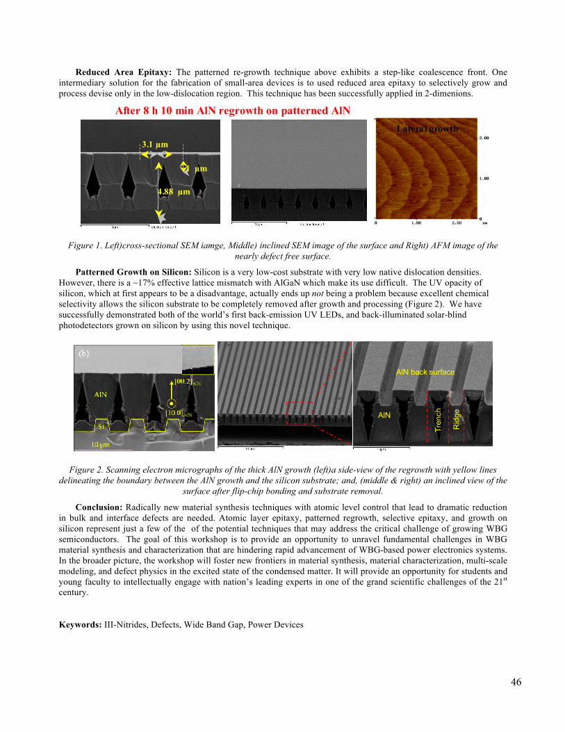
Reduced Area Epitaxy: The patterned re-growth technique above exhibits a step-like coalescence front. One intermediary solution for the fabrication of small-area devices is to used reduced area epitaxy to selectively grow and process devise only in the low-dislocation region. This technique has been successfully applied in 2-dimenions.
4.88 µm
3.1 µm
1 µm
After 3 h 40 min AlN regrowth on patterned AlN
2.64 µm
1.19 µm
After 8 h 10 min AlN regrowth on patterned AlN
3.4 µm
0.59 µm
5 h 10 min AlN regrowth on patterned AlN
Lateral growth
Coalescence area
Figure 1. Left)cross-sectional SEM iamge, Middle) inclined SEM image of the surface and Right) AFM image of the nearly defect free surface.
Patterned Growth on Silicon: Silicon is a very low-cost substrate with very low native dislocation densities. However, there is a ~17% effective lattice mismatch with AlGaN which make its use difficult. The UV opacity of silicon, which at first appears to be a disadvantage, actually ends up not being a problem because excellent chemical selectivity allows the silicon substrate to be completely removed after growth and processing (Figure 2). We have successfully demonstrated both of the world’s first back-emission UV LEDs, and back-illuminated solar-blind photodetectors grown on silicon by using this novel technique.
AlN
AlN back surface
Tren
ch
Rid
geAlN
AlN back surface
AlN
AlN back surface
Tren
ch
Rid
ge
Figure 2. Scanning electron micrographs of the thick AlN growth (left)a side-view of the regrowth with yellow lines delineating the boundary between the AlN growth and the silicon substrate; and, (middle & right) an inclined view of the
surface after flip-chip bonding and substrate removal.
Conclusion: Radically new material synthesis techniques with atomic level control that lead to dramatic reduction in bulk and interface defects are needed. Atomic layer epitaxy, patterned regrowth, selective epitaxy, and growth on silicon represent just a few of the of the potential techniques that may address the critical challenge of growing WBG semiconductors. The goal of this workshop is to provide an opportunity to unravel fundamental challenges in WBG material synthesis and characterization that are hindering rapid advancement of WBG-based power electronics systems. In the broader picture, the workshop will foster new frontiers in material synthesis, material characterization, multi-scale modeling, and defect physics in the excited state of the condensed matter. It will provide an opportunity for students and young faculty to intellectually engage with nation’s leading experts in one of the grand scientific challenges of the 21st
century.
Keywords: III-Nitrides, Defects, Wide Band Gap, Power Devices
46
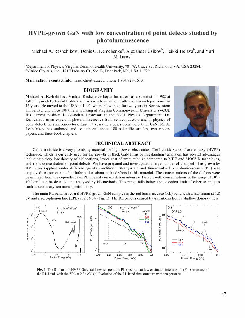
HVPE-grown GaN with low concentration of point defects studied by photoluminescence
Michael A. Reshchikova, Denis O. Demchenkoa, Alexander Usikovb, Heikki Helavab, and Yuri Makarovb
aDepartment of Physics, Virginia Commonwealth University, 701 W. Grace St., Richmond, VA, USA 23284; bNitride Crystals, Inc., 181E Industry Ct., Ste. B, Deer Park, NY, USA 11729
Main author’s contact info: [email protected]; phone 1 804 828-1613
BIOGRAPHY Michael A. Reshchikov: Michael Reshchikov began his career as a scientist in 1982 at Ioffe Physical-Technical Institute in Russia, where he held full-time research positions for 16 years. He moved to the USA in 1997, where he worked for two years in Northwestern University, and since 1999 he is working at Virginia Commonwealth University (VCU). His current position is Associate Professor at the VCU Physics Department. Dr. Reshchikov is an expert in photoluminescence from semiconductors and in physics of point defects in semiconductors. Last 17 years he studies point defects in GaN. M. A. Reshchikov has authored and co-authored about 180 scientific articles, two review papers, and three book chapters.
TECHNICAL ABSTRACT Gallium nitride is a very promising material for high-power electronics. The hydride vapor phase epitaxy (HVPE)
technique, which is currently used for the growth of thick GaN films or freestanding templates, has several advantages including a very low density of dislocations, lower cost of production as compared to MBE and MOCVD techniques, and a low concentration of point defects. We have prepared and investigated a large number of undoped films grown by HVPE on sapphire under different growth conditions. Steady-state and time-resolved photoluminescence (PL) was employed to extract valuable information about point defects in this material. The concentrations of the defects were determined from the dependence of PL intensity on excitation intensity. Defects with concentrations in the range of 1014-1016 cm-3 can be detected and analyzed by PL methods. This range falls below the detection limit of other techniques such as secondary-ion mass spectrometry.
The main PL band in several HVPE-grown GaN samples is the red luminescence (RL) band with a maximum at 1.8 eV and a zero-phonon line (ZPL) at 2.36 eV (Fig. 1). The RL band is caused by transitions from a shallow donor (at low
106
107
108
109
1.5 2 2.5 3 3.5
PL
inte
nsity
(rel
. uni
ts)
Photon Energy (eV)
Pexc
= 7x10⁻⁴ W/cm2
T=18 KRL band
ZPLUVL band
(a)
NBE
107
108
2.15 2.2 2.25 2.3 2.35 2.4
101102103106
PL
Inte
nsity
(rel
. uni
ts)
Photon Energy (eV)
Pexc
= 10-3 W/cm2
T = 18 K
LO2LO ZPL
sample(b)
107
108
2.25 2.3 2.35 2.4
18 K40 K50 K
PL
Inte
nsity
(rel
. uni
ts)
Photon Energy (eV)
DAP
eA
DAP-LO
eA-LO
*
*
(c)
Fig. 1. The RL band in HVPE GaN. (a) Low-temperature PL spectrum at low excitation intensity. (b) Fine structure of the RL band, with the ZPL at 2.36 eV. (c) Evolution of the RL band fine structure with temperature.
47

temperature) or from the conduction band (above 50 K) to an unknown deep acceptor having an energy level 1.130 eV above the valence band.
In high-quality GaN, including freestanding templates, one of the dominant defect-related PL band is the green luminescence (GL) band with a maximum at about 2.4 eV. Figure 2 shows the PL data for a 30-µm-thick GaN layer on
105
106
107
108
1.5 2 2.5 3 3.5
0.190.00013
PL In
tens
ity (r
el. u
nits
)
Photon Energy (eV)
T = 100 K
Pexc
(W/cm2)
RLGL
BLUVL
NBE(a)
x36
10-3
10-2
10-1
100
101
102
103
1.5 2 2.5 3 3.5
PL
inte
nsity
(rel
. uni
ts)
Photon Energy (eV)
T = 100 K Timedelay10-6s10-5s
10-4s
10-3s
10-2s1
2345
GL
YL
RL
BL
(b)
1010
1011
1012
1013
1014
1015
1016
1017
1018 1019 1020 1021 1022 1023 1024
GL bandYL bandUVL band
PL
inte
nsity
(rel
. uni
ts)
P0 (cm-2s-1)
T = 100 K(c)
Fig. 2. PL from high-quality GaN at T = 100 K. (a) Steady-state PL spectra at low and high excitation intensity. (b) Time-resolved PL spectra at different time delays after a laser pulse. Solid lines show simulated shapes for the GL band (1 and 2) and the YL band (3-5). (c) The dependence of the PL peak intensity after a laser pulse on the excitation intensity P0 for the GL, YL, and UVL bands. Solid lines are calculated with the concentration of defects N as the only fitting parameter. N = 5×1014 cm-3 for all three PL bands.
sapphire substrate. To reduce contribution from a very strong exciton emission (NBE), the data for defect-related PL are presented at 100 K and low excitation intensity. The PL spectrum includes the RL band, the blue luminescence (BL) band related to the ZnGa acceptors, and the ultraviolet luminescence (UVL) band with the main peak at 3.27 eV. The GL band increases as a square of the excitation intensity and becomes the dominant defect-related PL band at the excitation power density (Pexc) above 0.2 W/cm2. The GL band can be easily recognized in time-resolved PL measurements due to its exponential decay even at low temperatures, with a characteristic lifetime of 1-2 µs. The GL band is attributed to transitions of electrons from the conduction band to the 0/+ level of the isolated CN defect. The yellow luminescence (YL) band, related to transitions via the −/0 level of the same defect, has a maximum at 2.1 eV and can be observed only for some samples. Even when the YL band is not observed in the steady-state PL spectrum, it appears in time-resolved PL spectra at long time delays, after the GL band disappears (Fig. 2(b)).
The concentrations of the point defects responsible for the observed PL bands were determined from the dependences of the steady-state and time-resolved PL intensity on the excitation intensity. Figure 2(c) shows the dependences of PL intensity after a laser pulse on excitation intensity for three defect-related PL bands at 100 K. The solid lines are calculated. The concentration of point defects obtained from the fit is on the order of 1015 cm-3. The GL band intensity increases as a square of the excitation intensity (the dashed line in Fig. 2(c)) at low excitation intensity and saturates at high excitation intensity.
Keywords: GaN, photoluminescence, point defects
48

Structural and Chemical Characterization of The Transition Layer At The Interface of NO-annealed 4H-SiC/SiO2 Metal-Oxide-Semiconductor Field-Effect Transistors Lourdes G. Salamanca-Riba,1 Joshua A. Taillon,1 Claude A. Ahyi,2 John Rozen,3, John R. Williams,2 Leonard C. Feldman,3 Tsvetanka S. Zheleva,4 and Aivars J. Lelis,4 1 Materials Science and Engineering Department, University of Maryland, College Park, Maryland 20742, USA 2 Department of Physics, Auburn University, Auburn, Alabama 36849, USA 3 Department of Physics and Astronomy, Vanderbilt University, Nashville, Tennessee 37235, USA 4 US Army Research Lab, 2800 Powder Mill Road, Adelphi, Maryland 20783, USA Main author’s contact info: [email protected] (301)405-5220
BIOGRAPHY Lourdes Salamanca-Riba obtained her PhD degree in Physics from the Massachusetts Institute of Technology in 1985, she then became a senior research scientist at the General Motors Research Laboratory in Warren, MI. In 1987 she became an Assistant Professor in the Materials Program at the University of Maryland where she is now a full Professor in the Materials Science and Engineering Department.
Her research is in the areas of SiC wide band gap semiconductors, self-assembly of semiconductor nanowires and liquid crystal nanocomposites for hybrid photovoltaic applications, DNA-based biosensors and radiation sensors on GaAs, and materials with high C content in the form of nanocarbon called “covetics”.
TECHNICAL ABSTRACT SiC has been used to fabricate high power high frequency metal oxide semiconductor field effect transistors
(MOSFET) for high temperature operation where Si cannot be used. 4H-SiC is one of the many allotropes of SiC. It is a wide gap semiconductor with an energy gap of 3.23 eV at room temperature. SiO2 is a native oxide of SiC; just like for Si. Furthermore, SiC has a high bulk electron mobility. However, MOSFET devices based on 4H-SiC show a low carrier mobility. The lower mobility has been correlated to defects in the region surrounding the SiO2/SiC interface. These defects are electrically active and have energies within the band gap of the SiC leading to mobility reduction during inversion of the channel by field termination, carrier trapping and Coulomb scattering.1 Several defects, such as interstitial C, Si vacancies, O with three fold coordination and uncoordinated C and Si bonds, have been identified as possible candidates for the reduction of carrier mobility. Several investigators are attempting to reduce the density of defects in this interfacial layer called the “transition layer” by different processing methods during or after the growth of the SiO2 dielectric. One of the processes involves post-annealing of the thermally grown SiO2/SiC in NO atmosphere in order to induce carbon removal from the SiC and facilitate the formation of SiO2. Samples that underwent this NO annealing have shown increase in the carrier mobility.2,3 It is believed that N incorporates at the SiC/SiO2 interface giving rise to passivation of some of the defects in the transition layer by forming Si-N bonds.4
We have performed annealing of thermally grown SiO2/4H-SiC samples in an NO atmosphere for different periods of time to systematically investigate the role of annealing on the transition layer width. We characterized the interfacial region under the gate of the devices by high resolution TEM (HRTEM), high angle annular dark field (HAADF) imaging and electron energy loss spectroscopy (EELS). MOSFET devices with 150 µm n-channels were investigated in this study. The 4H-SiC wafers were (0001) Si face with a 4° miscut towards the < 112�0 > direction and had a doped SiC epitaxial layer with a doping concentration of ~5x10¹⁵/cm3. An approximately 55 nm thick oxide was grown by annealing the samples in dry O2 at 1,150 °C. The samples were post-annealed in NO at 1,175°C for various times up to 240 min. Samples for TEM analysis were prepared using an FEI Helios 650 focused ion beam/scanning electron microscope. The TEM lamellas were analyzed in a JEOL 2100 F field emission TEM operated at 200 kV and with a Gatan Tridiem electron energy loss spectrometer.
49

Figure 1 shows a typical HRTEM lattice image and diffraction pattern of a 4H-SiC/SiO2 sample that was annealed for 60 min. The image shows the high crystalline quality of the SiC and the amorphous SiO2 with a fairly sharp interface but with some contrast variations in the SiO2 region near the interface. Some contrast is also visible in the SiC region near the interface but it is difficult to estimate the thickness of the transition layer from these images. Instead, we estimated the width of the transition layer from EELS spectra obtained across the SiC/SiO2 interface. Figure 2 shows an example of the change of the Si-L2,3 signal as the beam is scanned from the SiC to the SiO2 in the HAADF image (Fig. 2(a)) of a sample annealed in NO for 60 min. The Si-L2,3 edge systematically shifts to higher energy as the beam is scanned from the SiC to the SiO2 (Fig. 2(b)). The spectra in Fig. 2(c) present the Si-L2,3 edge, the C-K edge and the O-K edge in the SiC (blue), interface (red) and SiO2 (yellow) taken from the corresponding colored rectangles in Fig. 2(a). The chemical shift of the Si-L2,3 edge is indicative of the change in the bonding of the Si atoms in the two materials. The distance in the sample perpendicular to the interface over which the Si-L2,3 shifted was used to estimate the width of the transition region, wTL.
5 The results presented in Fig. 3 for the different annealing times show that the transition layer
width systematically decreases with increasing annealing time. This result agrees with the increased mobility with annealing time obtained from the same samples.3 The chemical shift of the Si-L2,3 edge gives a good indication of the width of the transition region. Longer annealing in NO reduces the width of the transition region and increases the carrier mobility. Nitrogen incorporation at the interface has been reported in NO annealed films by passivation of Si dangling bonds and formation of Si-N bonds.4 Ours EELS spectra did not detect the N-K edge since nitrogen has been measured to be around 1x10¹⁴/cm2 from SIMS measurements.3
1 G. Y. Chung, et. al., Appl. Phys. Lett. 76, 1713 (2000). 2 T. L. Biggerstaff, et.al., Appl. Phys. Lett. 95, 032108 (2009). 3 J. Rozen, A. C. Ahyi, X. Zhu, J. R. Williams, and L. C. Feldman, IEEE Trans. Electron Devices 58, 3808 (2011). 4 Y. Xu, L. C. Feldman, et al., J. Appl. Phys., 115(3), 033502 (2014). 5 J.A. Taillon, et. al., J. Appl. Phys. 113, 044517 (2013).
Keywords: 4H-SiC, MOSFET, EELS, TEM, transition layer width, high power devices.
Fig. 1 [11�000] cross sectional HRTEM image and diffraction pattern from a 4H-SiC/SiO2 interface from a MOSFET annealed in NO for 60 min.
(a) (b)
(c)
Fig. 2 (a) HAADF STEM image of the 4H-SiC/SiO2 interface in the sample annealed for 60 min. (b) Si L2,3 edge shift as the beam is scanned across the interface in (a). (c) Spectra in the SiC, interface and SiO2 from the corresponding rectangular colored regions in (a) .
Fig. 3 Dependence of the width of the transition region with NO annealing time.
References:
50

Nanotechnology Enabled Defect Reduction in WBG Materials
Z. John Shena, Peter Parbrookb aIllinois Institute of Technology, Chicago, IL 60616, USA; bTyndall National Institute, Cork, Republic of Ireland
Main author’s contact info: [email protected]; phone 1 312 567-3352; iit.edu
BIOGRAPHY
Z. John Shen received BS from Tsinghua University, China, in 1987, and M.S. and Ph.D. degrees from Rensselaer Polytechnic Institute, Troy, NY, in 1991 and 1994, respectively, all in electrical engineering. Between 1994 and 1999, he held a variety of positions including Senior Principal Staff Scientist with Motorola. He was on the faculty of the University of Michigan-Dearborn between 1999 and 2004, and the University of Central Florida between 2004 and 2012. He joined the Illinois Institute of Technology in 2013 as the Grainger Chair Professor in Electrical and Power Engineering. He has held a courtesy professor appointment with Hunan University, China since 2007. His research interests include power electronics, power semiconductor devices and ICs, automotive electronics, renewable and alternative energy systems, and electronics manufacturing. He has published over 150 journal and conference articles, and holds 13 issued and several pending U.S. patents in these areas. Dr. Shen is a recipient of the 2012 IEEE Region 3 Outstanding Engineer Award, the 2003 NSF CAREER Award, the 2006 IEEE Transaction Paper Award from IEEE Society of Power Electronics, the 2003 IEEE Best Automotive Electronics Paper Award from IEEE Society of Vehicular Technology, and the 1996 Motorola Science and Technology Award. He has been an active volunteer in the IEEE Power Electronics Society (PELS), and has served as VP of Products 2009-2012, Associate Editor and Guest Editor in Chief of the IEEE Transactions on Power Electronics, technical program chair and general chair of several major IEEE conferences. He is an IEEE Fellow since 2011.
TECHNICAL ABSTRACT Gallium nitride (GaN) is a promising WBG semiconductor for photonic and power electronic applications. The research on GaN power devices has been predominantly focused on high electron mobility transistor (HEMT) type of lateral heterojunction devices fabricated on heteroepitaxial thin films on a foreign substrate. Unfortunately, GaN heteroepitaxial thin films grown on cost-effective but non-lattice-matched substrates such as silicon or sapphire suffer from detrimental crystal defects known as dislocations with a typical defect density of 107–1010 cm−2. These lattice-mismatch-induced dislocations increase the leakage current, disrupt the electric field distribution, and can result in premature microplasma breakdown—all of which compromise the reliability of these power devices and limit their commercialization prospects. Furthermore, today’s lateral HEMTs, limited by surface states and bulk defects, offer voltage and current ratings significantly below the theoretical potential of GaN. Vertical GaN device architectures free from material defects are highly desirable to push the power range of GaN to thousands of volts and hundreds of amperes.
Recently, one-dimensional nanostructures based on III-nitride semiconductors, including nanowires and nanorods, have attracted tremendous attention as potential nanoscale building blocks for improving performance of light-emitting diodes. Specifically, GaN nanowires offer the advantages of high light extraction efficiencies and the potential to be grown free of extended defects. GaN nanowires can elastically relax laterally, and accommodate lattice mismatch with Si substrate through pseudomorphic growth without dislocation formation as compared to thin-film heterostructures. Various reports have demonstrated the growth of dislocation-free, one-dimensional III-nitride nanostructures. The unique properties of GaN nanostructures grown with bottom-up fabrication, referred to as Fig. 1: GaN nano- or micro-rods on silicon
substrate developed for new LEDs by Aledia Inc. Source: http://www.aledia.com.
51

nano-GaN in this proposal, also present a great potential for developing transformative power device architectures offering high breakdown voltages, low leakage currents, and reliable device operation. However, this potential so far remains largely unexplored. Important scientific issues and technological barriers must be addressed in the areas of novel device architectures, controlled nanowire synthesis, improved understanding of structural, electrical, and thermal properties of nano-GaN, and nano-GaN device fabrication before the promise can be fully realized.
Unlike the lateral HEMT type of GaN power devices which have been researched extensively in the past decade, well-ordered arrays of small-diameter, straight GaN nanowires with naturally smooth surfaces (facets) would provide an interesting alternative for making high voltage vertical power devices. Potentially, the vertical nanowires offer an inherent advantage of achieving 5-10X higher breakdown voltages than the lateral HEMTs by exploiting three-dimensional electric field reduction techniques such as the super-junction concept. It is worth noting that the super-junction concept may be more naturally realized in vertical GaN nanowires than the multi-epi or mesa-etching approaches adopted in the commercial silicon super-junction power MOSFETs which have rapidly proliferated in the market in the past decade. However, the electrical properties of such nano-GaN structures remain relatively unexplored. Important scientific questions such as the mesa sidewall-related breakdown mechanisms, impact of sidewall surface states on carrier transport, and potential microplasma formation effects must be raised and investigated thoroughly before the commercial potential of nano-GaN power devices can be further explored.
GaN nanowires have a hexagonal wurtzite structure with quasi-cylindrical geometry, typically forming a hexagonal cross-section in line with the crystallography of the wire. If their potential is to be fully realized, a scalable synthesis process needs to be developed and optimized to allow precise control of the geometry (diameter, height, tip shape) and position of each nanowire, and to minimize dislocations. GaN nanowire structures can be fabricated using molecular beam epitaxy (MBE), or metalorganic vapor phase epitaxy (MOVPE), also known as metalorganic chemical vapor deposition (MOCVD). It has been hypothesized that III-nitride nanowires grown on (111) Si substrates accommodate the lattice mismatch at the hetero-interface through a dense network of dislocations that bend outwards, through a climb process to end at the free surface of the nanowire sidewall. It is assumed that threading dislocations can minimize their energy by bending and terminating at a free surface. This method of dislocation reduction has been observed experimentally and used to advantage in optoelectronic devices. Once this relaxation takes place, the nanowire grows keeping its own lattice parameter, a fact that is helped by the nanowire’s high surface-to-volume ratio. As a consequence, the nanowires grow without strain and are often reported as “dislocation-free”. However, detailed studies of the wire development during growth are still required to determine to what extent the dislocations are removed along the length of the nanowire.
In summary, high voltage vertical device architectures based on GaN nanowires offer a great potential to significantly improve the reliability and cost-effectiveness of WBG power semiconductors. However, the research in this area is still in its infancy, and there is a lack of fundamental understanding on nano- and micro-scale device design and modeling, nanoheteroexpitaxial materials growth, dislocations and characterization, as well as the effects of facet surface states on carrier transport and device breakdown properties. Many important scientific and practical issues remain to be explored.
Keywords: WBG, GaN, MOCVD, dislocations, power devices
Fig. 2: Hypothesis of threading dislocations (TD) reduction in GaN nanostructures by bending out to free surface during MOVPE growth.
N+ Si substrate
TD-‐freen-‐GaN
TD-‐freen-‐GaN
ThreadingDislocations bending out of nanowires
52

Basic Research Needs in Wide Bandgap (WBG) Power Semiconductors
K. Shenai
Energy Systems Division, Argonne National Laboratory, Argonne, IL 60439-4815 [email protected]; phone 1 630-252-3068; www.anl.gov
BIOGRAPHY Krishna Shenai earned his B. Tech. degree in electronics from the Indian Institute of Technology - Madras (India) in 1979, and MS and Ph.D. degrees in electrical engineering from the University of Maryland - College Park in 1981 and Stanford University in 1986, respectively.
Dr. Shenai is currently employed as the Principal Electrical Engineer within the Energy Systems Division at Argonne National Laboratory, Argonne, Illinois where he is leading the development and commercialization of wide bandgap (WBG) power electronics. For over 30 years, Dr. Shenai has made seminal contributions to power semiconductor materials and devices. His research has set industry standards for nearly three decades, and products developed based on his research have been generating multi-billion dollar annual sales revenues. In the 1980s, based on pioneering optimization of silicon power devices, Dr. Shenai proposed the use of WBG semiconductors for electrical power switching. He is a Fellow of IEEE, a Fellow of APS, a Fellow of AAAS, a Fellow of IETE (India), and a member of the Serbian Academy of Engineers. He has authored or co-authored some 400 peer-reviewed archival papers, 10 book chapters and 3 books. Dr. Shenai is a named inventor in 13 issued US patents.
TECHNICAL SUMMARY Concievably, the main benefits of using wide bandgap (WBG) semiconductor power switching devices in place of
traditional silicon power devices in low- (< 1.7 kV) and medium-voltage (1.7 kV to 6.5 kV) power electronics applications are increased energy efficiency, reduced power converter size, and prolonged field reliability [1]. However, commercially available WBG power devices made on silicon carbide (SiC) and gallium nitride (GaN) semiconductors have not found the market success that silicon power devices have enjoyed for the past five decades. Whereas the cost of a WBG power device ($/A for a given voltage application) is much higher compared to a silicon device with identical voltage and current ratings, it may be possible to offset the higher chip cost with increased energy efficiency and system-level cost and robustness benefits.
It is highly unlikely that the cost of a WBG power semiconductor chip is ever going to be smaller than that of a silicon power chip with identical voltage and current ratings. There are multiple factors that contribute to this hypothesis – starting material cost, manufacturing cost, and packaging cost are a few to name. Two major contributors for high cost of a WBG power device today are expensive starting material and poor manufacturing yield. This situation is complicated by the fact that the WBG manufacturers typically do not reveal the wafer yield or the methodology used to assess the yield. The factors that contribute to the poor wafer yield are also generally not known. What is true is that a relatively high leakage current in the blocking state causes significant voltage derating of a WBG power device. High cost of starting material stems from expensive crystal manufacturing process which requires costly materials, high growth temperatures, and long growth durations [2]. This scenario is unlikely to change in the forseable future unless a high throughput solution growth process similar to the Czochralski process [3] used for growing single crystal silicon is developed. Figure 1 is a pictorial illustration of the size difference between the silicon wafer ingot grown by the Czocharlski method [3] and SiC wafer grown by sublimation growth using the modified Lely process [2]. The silicon crystal is typically grown at a much lower temperature ( < 1,000°C) than the SiC crystal (> 2,000°C). The seeding of the
53

Fig. 1: Pictorial representation of a silicon wafer ingot grown by the Czochralski method [3] and SiC wafer grown by sublimation growth using the modified Lely process [2].
Fig. 2: Measured breakdown voltage, VBR(DSS) vs. junction temperature, Tj(ºC) for a 1,200V/50A commercial SiC power MOSFET. For comparison, datasheet values are also shown along with measurement conditions.
crystal in a SiC growth process begins with threading screw dislocations (TSDs). Hence, to obtain commercially viable crystal growth rates for SiC, a minimum number of TSDs are needed and the growth must be performed at a much higher temperature than silicon. These inherent material synthesis limiations lead to a high density of crystal defects in the SiC substrate material compared to silicon substrates. Silicon defect density for the past many decades has been steady below 1 defect/cm2. The starting material problem presents a fundamental limitation in the large-scale commercialization of WBG power devices especially for high-volume applications such as electric vehicles which by one estimate demands several million wafers per year by 2,020.
Figure 2 is a plot of the measured breakdown voltage V(BR)DSS vs. junction temperature Tj(°C). As seen from the datasheet value for breakdown voltage, it is clear that commercial devices are de-rated by a factor of 0.68. In comparison, typical silicon power MOSFETs are de-rated by a factor of 0.85. The SiC power MOSFETs are de-rated by a larger factor than silicon devices because increased leakage currents in the off-state due to space-charge generation and recombination at defect sites prevent these devices to be operated in the near avalanche regime. Figure 3 illustrates the measured body diode characteristics of a SiC power MOSFET at 150°C. Unlike a silicon power MOSFET, the SiC power MOSFET shows a strong dependence of body diode conduction on gate-source voltage that indicates the presence of excessive oxide charge. A careful review of commercial products has revealed that unlike silicon power MOSFET datasheets, SiC power MOSFET datasheets do not list drain dv/dt ratings. This is an important parameter since high-voltage SiC power MOSFETs are switched in nano seconds. For example, it is typical to find a drain dv/dt rating of at least 15 V/ns in the case of silicon power MOSFETs at Tj = 150°C. Available experimental data for SiC JBS diodes suggests a very low dv/dt rating of < 7V/ns at Tj = 150°C [4]. This is a serious concern that must be addressed in order to assess the long-term field-reliability of SiC power devices in compact high-density power converters. Another reliability parameter of interest is the single
pulse avalanche energy, EAS. A survey of the commercial product datasheets reveals that typical reported values of EAS at Tj = 25°C are 2 Joules (measured at half the rated current) and 1 – 2.2 Joules (measured at half the rated current for VDD = 150 V and 50 V, respectively) for 1,200V silicon and SiC power MOSFETs, respectively. Figure 4 is a plot of measured EAS for silicon and SiC power diodes which shows even smaller avalanche energy capability for SiC power diodes than silicon power diodes. More data needs to be generated under identical measurement conditions at elevated junction temperatures in order to critically evaluate dv/dt and EAS capabilities of WBG power devices and bench-mark against silicon power devices with identical ratings.
Figure 5 is a plot of the safe operating area (SOA) reported in the datasheets for commercial 1,200V silicon and SiC power MOSFETs at room temperature; all three devices have nearly the same current ratings. The SOA plots of three devices have distinct shapes indicating packaging and thermal variations. The SOA of silicon power MOSFET is higher than that of either SiC power MOSFETs. This observation is particularly important since SiC devices are expected to demonstrate superior SOA than silicon devices because of improved electrical and thermal material properties. The stability of the gate threshold voltage [5] and the reliability of body diode
54

Fig. 3: Measured body diode forward on-state characteristics Tj = 150°C for a 1,200V/50A commercial SiC power MOSFET. A strong gate-source voltage dependence on body diode conduction can be seen suggesting an excessive oxide charge.
Fig. 5: Measured safe operating area (SOA) of 1,200V/30A silicon power MOSFET, and 1,200V/32A and 1,200V/45A SiC power MOSFETs at Tj=25°C.
Fig. 4: Measured avalanche energy capabilities of 600V/6A silicon MPS diode and 600V/8A SiC JBS diode at 25°C.
Fig. 6: Measured concentration of carbon vacancy in as-grown 4H-SiC with conventional annealing in an inductively heated furnace at various temperatures for 5 min. duration.
[6] and gate oxide [7] of a SiC power MOSFET have been extensively studied in the literature. A negative shift in the
MOS gate threshold voltage under high-temperature reverse-bias (HTRB) stress has been shown to cause an increase in the off-state leakage current and potential device failure. A large positive shift of the MOS gate threshold voltage under high-temperature gate-bias (HTGB) conditions with a positive bias-temperature stress can also lead to a significant increase in the on-state resistance and thus a decrease in device efficiency. The local “hot spots” are caused by the formation of micro plasma that leads to device destruction. Crystal defects introduce local potentials in the
semiconductor crystal lattice that strongly distort the energy-band structure of WBG semiconductors and cause severe degradation in electrical parameters in the excited state of the condensed matter. However, fundamental understanding of the exact phenomena of the excited state of condensed matter is lacking. This phenomenon is particularly important in high-voltage (> 6.5 kV) bipolar SiC power devices where in addition to TSDs and TEDs, point defects such as the carbon vacancy (VC) have been found to have catastrophic effects on high-voltage bipolar power diodes. For example, VC which is a prime life-time controlling defect through its Z1/2 state [8] and is found to increase in its concentration when high processing temperatures in excess of 1600°C are used [9]. Such high processing temperatures are essential for fabricating high-voltage (6.5 kV – 65 kV) SiC
55

bipolar power devices where selective p-type doping using group-III elements, like B and Al, is employed using the process of ion implantation.
In summary, the challenges facing the WBG power semiconductor community are essentially basic and fundamental in nature. The high cost, poor performance and degraded reliability stem from the starting material used in the manufacturing process as it is prohibitively expensive compared to silicon, and contains a very high density of crystal defects. The exact role that these defects play on device performance and reliability is unknown, especially under the excited state of the condensed matter where most power devices are operated. The excited state may be caused by a combination of high-level charge injection, high temperature, and high electric field. This information is critical in order to optimize the manufacturing technology and also to develop new low-temperature materials synthesis techniques that result in low defect density at high throughput rates.
REFERENCES 1. K. Shenai, R. S. Scott, and B. J. Baliga, "Optimum semiconductors for high-power electronics," IEEE Trans.
Electron Devices, vol. 36, no. 9, pp. 1811-1823, Sept. 1989.
2. J. A. Lely, "Sublimation process for manufacturing Silicon Carbide crystals," U.S. Patent 2,854,364, issuedSeptember 30, 1958.
3. W. Lin and K. E. Benson, “The science and engineering of large-diameter Czochralski silicon crystal growth,”Ann. Rev. Mater. Sci.1987.17: 273-98.
4. K. Acharya and K. Shenai, “On the dv/dt rating of SiC Schottky power rectifiers,” Proc. Power ElectronicsTechnology Conference, October 2002, pp. 672-677.
5. A. J. Lelis, D. Habersat, R. Green, A. Ogunniyi, M. Gurfunkel, J. Suehle, and N. Goldsman, “Time dependenceof bias-stress-induced SiC MOSFET threshold-voltage instability measurements,” IEEE Trans. Electron
Devices, vol. 55, no. 8, p. 1845, 2008.
6. A. Agarwal, H. Fatima, S. Haney, and S. –H. Ryu, “A new degradation mechanism in high-voltage SiC powerMOSFETs,” IEEE Electron Device Letters, vol. 28, no. 7, p. 587, 2007.
7. L. C. Yu, G. Dunne, K. Matocha, K. P. Cheung, J. Suehle, and K. Sheng, “Reliability issues of SiC MOSFETs:A technology for high-temperature environments,” IEEE Trans. Device and Materials Reliability, vol. 10, no.4, p. 418, 2010.
8. T. Kimoto, G. Feng, T. Hiyoshi, K. Kawahara, M. Noborio, and J. Suda, Mater. Sci. Forum 645-648, 645(2010).
9. H. M. Ayedh, V. Bobal, R. Nipoti, A. Hallen, and B. G. Svensson, “Formation of carbon vacancy in 4H siliconcarbide during high-temperature processing,” J. Appl. Phys.115, 012005 (2014).
Keywords: Wide bandgap (WBG) power semiconductors, dislocations, stacking faults, point defects, performance, reliability, cost, manufacturing, basic research
56

Nondestructive Assessment of Surface and Subsurface Defects in Wide-bandgap Semiconductors using Photon Back Scattering
Elena Guliants, Guru Subramanyam, and Fred D. Orazio
Center of Excellence for Thin film Research and Surface Engineering (CETRASE), University of Dayton, 300 College Park, Dayton, OH 45469-0232 Main author’s contact info:[email protected], Phone: 937-229-3188
BIOGRAPHY Guru Subramanyam: Guru Subramanyam is currently a Professor and the Chair of the Department of Electrical and Computer Engineering, at the University of Dayton. He obtained his B.E. (EE) from University of Madras in 1984, with first class and distinction. He obtained his MS (1988) and PhD (1993) degrees in EE from University of Cincinnati with specialization in Microelectronics. He has published over 150 refereed journal and conference papers in the areas of electronic materials. His current research involves tunable high-k dielectrics, GaN varactors, Memristors, and bio-polymers for electronics, and photonics. He has been collaborating with the Air Force Research Laboratory (AFRL) in these research areas since 2000. His work to date has been funded by NASA, AFRL, AFOSR, NSF, and DARPA. Professor Subramanyam won the 2008 Alumni Award for Scholarship at the University of Dayton, 2007 IEEE Dayton section Harrell Noble Award for his achievements in electronic devices, and 2007 UD Sigma Xi's 2007 George Noland Research Award. He is a Senior Member of IEEE.
Technical Abstract
The effort to produce defect free materials for semiconductor applications continues into the realm of wide bandgap semiconductors such as silicon carbide (SiC) and gallium nitride (GaN). These materials are critical for semiconductor devices intended for use in high-voltage, high-temperature and other extreme applications. There are two types of defects that must be considered. The first type represents defects that are grown into the bulk material typically used as the substrate for building power semiconductor devices. These are individual crystal defects that are distributed throughout the bulk of the material during crystal growth. The second type represents defects that are generated by the surface finishing process used to manufacture the semiconductor wafers. These defects are concentrated near the surface and can easily include impurities from the various materials that come into contact with the surface during processing. They are typically lumped together and called subsurface defects because they rarely extend more than a few microns below the surface. Both types of defects will affect the performance and reliability of the devices made on these wafers.
It is known that the two types of defects mentioned above can easily affect leakage currents, switching speeds and the lifetime of devices. The University of Dayton has a unique, non-destructive method of material characterization called the PBS measurement (sometimes called photon back-scattering). The PBS measurement uses scattered laser light in the ultraviolet (UV) to detect and map surface and subsurface defects on wafers made from these wide bandgap materials.
The PBS measurement is designed to allow penetration of the laser light into the material and detect the scattered light from the defects below the surface. The measurement can also separate surface from subsurface defects and provide color maps of the defects on areas up to 100 mm in diameter. The UV wavelength (325 nm) is used because these materials are generally opaque in the UV and the probe beam penetrates only a very short distance into the material. For SiC, defects can be detected to a depth of ~7 microns, and for GaN defects can be detected to a depth of
57

~0.13 microns. This limits extraneous scatter from other surfaces and insures that only defects near the surface are detected.
Examples of PBS measurements on SiC are shown in Figures 1. The measurement units are ppm/Sr (Parts-Per-Million-Per-Steradian), the units of scattered light. (Note that this is not total integrated scatter (TIS) that uses units of ppm. TIS cannot separate the subsurface scattered light and provides little detail.) The color scale at the side of the map shows the correlation between color and scatter level. The colors and some features look similar on these two maps, but the upper scale limit is quite different, as are the averages, indicating very different levels of subsurface damage.
Figure 1. Color Map of a 50 mm Diameter SiC Wafer Showing Severe Linear Processing Damage.
The red lines on these maps indicate linear damage from processing, sawing, grinding and even polishing. Isolated red spots indicate point defects of various kinds, while the larger red areas are other types of processing defects. These maps are from wafers produced several years ago and the state of the art has certainly improved. In these maps, any bulk crystal defects are hidden by the processing subsurface damage. Once the processing damage is minimized, the effect of the bulk crystal defects will be seen. The current equipment can detect scatter down to 0.001 ppm/Sr so even low levels of defects should be detectable.
Keywords: Photon backscattering, defects in semiconductors, non-destructive testing of semiconductors
58

Defects in 4H-SiC epitaxial growth using tetrafluoridesilane as Si precursor
Tangali S. Sudarshan, Haizheng Song, M.V.S. Chandrashekhar
Department of Electrical Engineering, University of South Carolina, Columbia, South Carolina 29208, USA
T. S. Sudarshan: [email protected]; Phone: 803.777.5174; Website: http://www.ee.sc.edu/research/SiC_Research/
BIOGRAPHY T. S. Sudarshan: received B.Sc. degree in physics, mathematics, and chemistry from the University of Bangalore, Bangalore, India, in 1968, M.Sc. degree in physics (solid state) from the University of Mysore, Mysore, India, in 1970, and the M.A.Sc. and Ph.D. degrees in electrical engineering from the University of Waterloo, Waterloo, ON, Canada, in 1972 and 1974, respectively.
He is currently Carolina Distinguished Professor Emeritus in the Department of Electrical Engineering, University of South Carolina. His research interest includes SiC CVD film growth, defect engineering and characterization; novel techniques of SiC bulk growth, wafering, surface preparation and defect characterization; SiC material and device processing; device fabrication and characterization.
TECHNICAL ABSTRACT Chemical vapor deposition (CVD) is the most mature process for the production of SiC epitaxial films. In the
conventional SiC-CVD process using silane as the Si-precursor, the growth rate for high quality SiC film is generally about 5-10 μm/h. Increase of the growth rate, essential for the production of thick films >50µm for high power electronics, is restricted due to Si gas phase nucleation at high silane concentration, which leads to generation of Si droplets [1]. The Si droplets will be carried to the growing surface by the carrier gas, creating defects and degrading crystal quality. To overcome this problem, chloride-based compounds were introduced to replace silane as the Si precursor [1]. However many challenges still remain for achieving high quality thick SiC epitaxial films at high growth rates and/or long growth duration. Defect generation caused by “parasitic deposition” has been reported to be a limiting factor in achieving high quality epilayers [2-4]. The parasitic deposition in CVD process occurs due to early gas phase decomposition of the precursors at temperatures lower than the substrate temperature, which causes deposition of the decomposed spices (Si and SixCy) on the wall of reactor parts (such as the gas injector and the hot-wall) prior to reaching the substrate [3]. Particulates formed due to parasitic deposition are generally loosely bound on the wall, and can be carried to the growth surface during growth, resulting in degradation of crystal quality by introducing defects in the growing epitaxial layers. This phenomenon is specifically severe at higher precursor gas flow rates or in long duration growth required to achieve thick epilayers. In SiC CVD growth using traditional silane or chloride-based precursors, the parasitic deposition cannot be effectively reduced because the decomposition temperatures of silane or chloride-based precursors are too low compared to the epigrowth temperature (~1600°C). Therefore, the solution to restriction/elimination of the parasitic deposition is to find a suitable precursor that decomposes only in the vicinity of the substrate.
Recently, studies at the authors’ group demonstrated that tetrafluorosilane (TFS), a fluorinated silane, is a promising candidate to replace the currently used silane or chlorinated silane gases as the Si precursor to significantly reduce the parasitic deposition, and hence to achieving very low defect density SiC epilayers [2]. The Si-F bond strength in TFS is the highest among all halogenated silanes, which allows complete elimination of Si-Si bond formation (Si-droplet) and significant suppress early decomposition of the precursor (parasitic deposition). As shown in Fig. 1, this unique CVD process using TFS as the precursor can completely eliminate silicon gas phase nucleation (in the condition of H2 with only Si precursor gas flow) and reduce the overall parasitic deposition by 80% (in the condition of H2 with both C and Si precursors) compared to the conventional SiC CVD process using silane or chlorine based silicon (e.g., dichlorosilane, DCS) precursors.
59

Attributed to the reduction of parasitic deposition, SiC epitaxial growth using TFS shows significant reduction of particle and growth pit densities (Table 1). It is also interesting to see that the epilayers grown using TFS have lower densities of basal plane dislocation (BPD) and in-grown stacking fault (IGSF), as well as a higher crystalline quality, compared with the epilayers grown using silane or DCS.
Growth of SiC on low off-axis (<= 4°) usually generates surface step bunching. The TFS grown epilayers exhibit better surface morphology with less step bunching. In AFM characterizations, the TFS grown epilayer has a RMS value of 1.3 nm and a macro step height of ~2 nm (~8 bilayers), while the DCS grown epilayer has the RMS value of 2.2 nm and the macro step height of ~8 nm (~32 bilayers).
Systematic study of the effect of C/Si ratio on the epilayer quality and defect density in SiC epitaxial growth using TFS will be presented. Further reduction of BPD density or complete elimination of BPDs on SiC epilayers has been achieved when the epitaxial process is combined with suitable substrate etching in KOH-eutectic and hydrogen pretreatment.
(a) (b)
Figure 1. The mass of parasitic deposition on the gas injector wall using silane, DCS or TFS precursor gases (a) with and (b) without propane addition [2].
Table 1. Comparison of defects on 8° SiC epilayers grown using silane, DCS and TFS gases [3].
Si precursor
Flow rate
(sccm)
Growth rate
(μm/hr)
XRD FWHM
BPD (cm-2)
TED (cm-2)
TSD (cm-2)
IGSF (cm-2)
Large Particle
100–400 µm (cm–2 )
Medium Particle
30–100 µm (cm–2 )
Small Particle
10–30 µm (cm–2 )
Growth Pit
(cm–2 )
Silane 5 7 ~20 233-625 2 x 10⁴ 960 912-1800 ~20 ~50 ~200 3 × 10⁵ DCS 5 10 ~12 144-388 2 x 10⁴ 1060 242-1000 0 ~45 ~100 2 × 10³ TFS 10 30 ~7.5 14-22 1 x 10⁴ 1050 92-100 0 0 ~5 ~50
Keywords: Silicon carbide, chemical vapor deposition, epitaxial growth, parasitic deposition, defects, Si-droplets, tetrafluoridesilane
References: [1]. H. Pedersen, S. Leone, O.Kordina, A.Henry, S. Nishizawa, Y.Koshka, E. Janzen, Chemical Reviews, 112, 2434 (2011). [2]. T. Rana,M. V. S. Chandrashekhar, T. S. Sudarshan, Physica Status Solidi A, 209, 2455 (2012). [3]. T. S. Sudarshan, T. Rana, H. Song, M.V.S. Chandrashekhar, ECS Journal of Solid State Science and Technology, 2 (8), N3079 (2013). [4]. J. J. Sumakeris, M. J. Paisley, M. J. O'Loughlin, US Patent, US 7,118,781 B1, (2006).
60

Self-oriented growth of Gallium Nitride on molten Gallium for large single crystals
Mahendra K. Sunkara Conn Center for Renewable Energy Research and Chemical Engineering, University of Louisville, Louisville, KY 40292
Main author’s contact info: [email protected]; phone 502 852 8574; http://www.conncenter.org
BIOGRAPHY Principle Author Name: Dr. Mahendra K. Sunkara is currently a Professor of
Chemical Engineering, Distinguished University Scholar and the Director for the Conn Center for Renewable Energy Research (Conn Center) at University of Louisville. Dr. Sunkara received his B. Tech. degree in Chemical Engineering from Andhra University (India) in 1986 and M.S., Ph. D. degrees in Chemical Engineering from Clarkson University in 1988 and Case Western Reserve University in 1993, respectively. His PhD dissertation work was focused on chemical vapor deposition of diamond under the guidance of Professor John Angus. He worked at Faraday Technology, Inc. in Dayton, OH from 1993-1996.
He joined UofL in 1996 and has established a research lab focused on diamond and related materials. His current research interests include renewable energy technologies such as solar cells, Li Ion batteries, production of hydrogen from water and process development for growing large crystals of diamond, gallium nitride and bulk quantities of nanowires, novel carbon morphologies. He has published over 100 articles in refereed journals and proceedings, four book chapters and was awarded ten U.S. patents along with several additional U.S. patent applications pending. He co-authored a book entitled “Inorganic Nanowires: Applications, Properties and Characterization” published by CRC Press. Several national and international news articles appeared on his research work in the area of nanoscale materials and their use in energy conversion and storage applications. In the last ten years, Dr. Sunkara delivered over fifty invited and keynote lectures in Germany, US, Greece, Taiwan, Slovenia and India. Four of his research articles appeared on the covers of prestigious journals, Advanced Materials, Advanced Functional Materials, Chemical Communications and Carbon. He was awarded the Ralph E. Powe Junior Faculty in Engineering award in 1999 and was the first recipient of the prestigious CAREER grant in Speed School from the National Science Foundation in 1999. In 2002, the Louisville Magazine placed him in the list of top 25 young guns in the city of Louisville. In 2009, he received the UofL President’s distinguished faculty award for research and United Phosphorus CDS Award from the Indian Institute of Chemical Engineers in December 2009. His technology on scalable manufacturing of nanowires is being commercialized through a startup, Advanced Energy Materials, LLC.
TECHNICAL ABSTRACT
A process is presented for obtaining large area, bulk grown, single crystals of Gallium Nitride (GaN). This process involves the use of low-pressure plasmas for nitrogen dissolution and crystallization of GaN out of Ga melts. Free standing films of 20 micron thick over areas larger than 10 mm x 10 mm have been produced from the laboratory process. Further homo-epitaxial growth of GaN on these substrates can be used to produce free-standing wafers for device fabrication. The development of technologies that have the potential to produce freestanding substrates of wide band gap materials will allow for producing next generation power electronics devices and systems.
Large area oriented GaN flakes of sizes few mm by few mm as shown in Fig. 10(a) &(b) were obtained when mm thick gallium film was nitrided. The gallium nitride crystals joined together with indiscernible boundaries and layer by layer growth started after joining. The largest
61

flake had the area exceeding 10 mm x 10 mm at a thickness of over 10 microns. See optical photographs of the flakes produced in Figure 1.
Figure 1: (a) optical graph of oriented GaN flakes with mm thick gallium growth; (b) SEM images showing joining of GaN platelets, inserted is the XRD spectrum.
The XRD texture analysis of the free standing GaN flakes with areas over 25 mm2 exhibited an overall c-axis tilt of 2.2o while showing primary reflections from (0002) and (0004) planes. Further more, the cross-sectional TEM micrographs showed that the resulting GaN films are free from dislocation crops inside the grains but showed diffraction contrast due to small misorientation between the grains. The twist and tilt angles between adjacent columnar grains were determined using convergent beam electron diffraction technique to be less than 8o and 1o, respectively. HRTEM micrographs of the grain boundaries showed sharp interfaces with both twisted and perfect attachments. Figure 2 shows XRD pattern analysis of films growth on molten Ga and quartz substrates showing highly textured growth on molten Ga and polycrystalline film growth on quartz substrate.
Figure 2: XRD pattern of GaN films obtained under two different wetting conditions of molten Ga: (a) Ga wets the substrate and (b) Ga partially wets the substrate during nitridation.
The experiments were conducted in a vacuum chamber equipped with stationary ceramic heating stage and ECR-MW plasma source. As we ramped up the temperature, the gallium film on quartz substrates agglomerated into droplets with a considerable size distribution. These gallium droplets started to spread after about 10 minutes’ exposure to atomic nitrogen at 950 oC. Gradually, the nitrogenated gallium melts covered the substrate and a thin, gray colored solid film eventually formed on top of a gallium layer. The spreading of gallium melts was found to be critical in forming the self-oriented films.
Keywords: Bulk growth, GaN wafers, low pressure, plasma nitridation
0
4000
8000
12000
16000
20 30 40 50 60 70 80 902 θ
Inte
nsity
(A.U
.)
(0002)
(0004) 0
1000
2000
3000
4000
5000
6000
7000
8000
20 30 40 50 60 70 80 902θ
Inte
nsity
(A.U
.)
(1010)
(0002)
(1011)
(1120)
(a) (b)
62

Detection and Mitigation of Surface Defects in
Transfer-Doped, Single-Crystal Diamond Films
A. Glen Birdwell, Frank J. Crowne , Mariela Georgieva, Tony G. Ivanov, Terrance P. O’Regan, Pankaj B. Shah , James D. Weil
aArmy Research Laboratory (Adelphi Laboratory Center), 2800 Powder Mill Road, Adelphi, MD USA 20783
Main author’s contact info: [email protected]
BIOGRAPHY Mr. James Weil is a member of the Emerging Electronics team at the Army Research Laboratory’s Adelphi Laboratory Center in Adelphi, Maryland. Weil’s research is focused on building high-mobility, high current devices on diamond.
Prior to the Army Research Laboratory, Weil started his career as a member of the technology development team at IBM’s Microelectronics Division and served as a lead process engineer for Micron Technology’s 300mm pilot operations and volume manufacturing teams. Most recently, he served as Senior Principal Semiconductor Engineer with the BAE Systems Semiconductor Technology Center (STC) in Manassas Virginia. With sixteen years of increasing contributions in private industry and military defense systems, Weil’s experience extends to state-of-the-art CMOS devices, radiation-hardened devices, chalcogenide-based RAM, photonics, MEMs-based thermal detectors, electron detectors, and nano-electronic devices.
He holds a M.S. in Materials Science and a B.S. in Applied Physics, both from Michigan Technological University. His graduate research with Professor Mohan Krishnamurthy focused on molecular beam epitaxial growth and morphological evolution of Silicon-Germanium quantum structures.
TECHNICAL ABSTRACT Our modeling suggests surface roughness is the primary contributor to mobility degradation of transfer-doped, diamond transistors. During the initial steps of diamond device fabrication, bulk and surface defects are introduced. With subsequent processing, these defects may become apparent in the surface channel region of the device. Consequently, detection and elimination of defects occurring within the initial steps of fabrication becomes a fundamental objective for establishing an atomically flat, high-mobility surface channel.
Our research is focused on characterizing and eliminating sources of such defects in CVD-grown diamond substrates. In particular, we will present results for various time and temperature conditions for hydrogenation of CVD-grown <100> diamond surfaces.
Keywords: CVD Diamond, hydrogenation, 2D hole gas, mobility, transfer doping, surface roughness.
63

Principles of bulk SiC growth by the Large Tapered Crystal growth process
Andrew A. Woodworth a, Andrew J. Trunek b, Philip G. Neudeck b, David J. Spry b, Ouloide Goue c, Balaji Raghothamachar c and Michael Dudley c
a NASA Glenn Research Center, 21000 Brookpark Road, MS 106-1, Cleveland, OH 44135, USA b NASA Glenn Research Center, 21000 Brookpark Road, MS 77-1, Cleveland, OH 44135, USA c Department of Materials Science & Engineering, Stony Brook University, Stony Brook, NY 11794-2275, USA
Andrew Woodworth’s contact info: [email protected], (216) 433-3544
BIOGRAPHY Andrew A. Woodworth PhD is currently a Research Physicist at the NASA Glenn Research Center responsible for single crystal silicon carbide (SiC) fiber growth using the solvent-laser heated floating zone (solvent-LHFZ) technique. He earned a Ph.D. in physics from West Virginia University (WVU) while investigating the effects of surface preparation on the interaction of thin metal films with 6H-SiC. While a graduate student at WVU Dr. Woodworth also worked as a Physical Scientist National Institute for Occupational Safety and Health (NIOSH) studying particulate surfaces. After gaining his Ph.D. Dr. Woodworth took a Postdoctoral Fellowship with the Chemical Engineering Department at WVU and eventually took a position as a Staff Scientist with the West Virginia Nano Initiative. Later he competed for and won a NASA Postdoctoral Fellowship at the NASA Glenn Research Center. While a NASA Postdoctoral Fellow Dr. Woodworth developed the Solvent-LHFZ growth technique to produce single crystal SiC Fibers.
TECHNICAL ABSTRACT Some important limitations to high-field silicon
carbide (SiC) power device electrical performance properties has been linked to the high number (>2000/cm2) [1] of screw dislocations (SD) in commercially available SiC wafers [2,3]. Researchers at the NASA Glenn Research Center have proposed an alternative method to mass-produce significantly higher quality bulk SiC. This alternate growth method requires defect assisted growth of a single screw dislocation in the c-axis direction into a long 4H-SiC single crystal fiber. The single crystal fiber is then drawn through a chamber where it is laterally enlarged (perpendicular to the c-axis) via a chemical vapor deposition (CVD) process into a large tapered crystal (LTC) [4]. The result is expected to be a large single crystal boule with a SD at the center. In order for this bulk growth method to become reality, the principles of each step are being studied in order to develop a process capable of creating the large tapered crystal as described in US patent 7,449,065 B1.
The LTC process can be split into two pieces: vertical growth of a single crystal fiber and lateral epitaxial growth of a single crystal fiber. The solvent-Laser Heated Floating Zone (solvent-LHFZ) crystal growth technique was developed in order to
Lateral Growth Process:CVD growth to enlarge fiber sidewalls into large boule.- 1600 C, lower stress- Only 1 dislocation
Vertical & Lateral growth are simultaneous & continuous (creates a tapered shape).
[0001] c-direction
<1120> a-direction
<1100> m-‐direction
Vertical Growth Process:Elongate small-diameter fiber seed grown from single SiC dislocation.
The Large Tapered Crystal Process [4]
64

form single crystal SiC fibers necessary for the first step in the LTC process. Solvent-LHFZ combines the fiber growth capabilities of laser heated floating zone with the traveling solvent growth method’s ability to grow SiC. So far the solvent-LHFZ has been shown to grow epitaxial SiC, but has yet to grow a single crystal fiber. The lack of a well ordered growth front established by the seed crystal has to date been a major impediment to single-crystal fiber growth. Developing improved seed crystals with more ordered growth front for this technique is currently under investigation.
Lateral growth is currently under investigation in a hot wall chemical vapor deposition (CVD) reactor. CVD experiments, using seed crystals that mimic single crystal fibers, have produced single crystals wider than 4 mm and replicate the underlying polytype. However the grown crystals contain large bundles of defects emanating from the seed crystals. At this time, results are unclear as to whether the defects are an extension of defects contained previously in the seed crystals or a result of the CVD process. Currently lateral growth efforts are centered on using higher quality (lower defect density) crystals that simulate single crystal fibers in order to determine the source of the defects.
[1] J. Zhang, et al., Mater. Sci. Forum, 717 (2012) 137-140 [2] R. Berechman, et al., J. Appl. Phys., 107 (2010) 114504. [3] P. G. Neudeck et al., Solid-State Elec., 42, 1257 (1998). [4] J. A. Powell, et al., U.S. Patent 7,449,065 issued November 11, 2008. [5] A. A. Woodworth, et. al., Mater. Sci. Forum, 717 (2012) 49-52. Keywords: Silicon Carbide, Crystal Growth, Screw Dislocation, Single Crystal, Bulk Growth, Fiber Growth, Chemical Vapor Deposition, Laser Heated Floating Zone
Solvent-Laser Heated Floating Zone Technique [5]
Laterally Grown SiC Crystal
Hot-Wall Chemical Vapor Deposition Reactor
65

The role of surface kinetics on surface morphology and defect evolution during WBG semiconductor epitaxy
A. Yanguas-Gila,b, K. Shenaia,b aArgonne National Laboratory, 9700 S Cass Ave, Lemont IL USA 60439; bNorthwestern-Argonne Institute for Science and Engineering (NAISE), Northwestern University, Evanston IL USA 60208.
Main author’s contact info: [email protected]; phone 1 630 252-7353;
BIOGRAPHY Angel Yanguas-Gil: Born in Sevilla, Spain, in 1978, he is currently a Principal Materials Scientist at the Energy Systems Division at Argonne National Laboratory and a Fellow of the Northwester-Argonne Institute for Science and Engineering. He carried out his PhD research at the Spanish National Research Council in the fields of thin film growth and plasma physics, obtaining his PhD degree at the University of Seville in 2007. After being a postdoc at the Physics department of the Ruhr University-Bochum (Germany) and the Department of Materials Science and Engineering of the University of Illinois at Urbana-Champaign, in 2009 he joined Argonne as an Assistant Materials Scientist, becoming a Principal Materials Scientist in 2013. He has published over 35 peer-reviewed articles and 2 book chapters, and he is the author of 7 patents, patent applications and invention disclosures. His research focuses on the mechanistic aspects of thin film growth, and the interplay between kinetics, microstructure, and thin film properties, both from an experimental and theoretical point of view. His interests range from fundamental in-situ characterization studies to process development and scale up. He is a member of the scientific committee and guest editor of the special issue of the 56th Electronic Materials Conference and is a reviewer for journals in the fields of materials science, chemistry, and physics.
TECHNICAL ABSTRACT One of the big gaps in our knowledge of MOCVD and CVD of wide bandgap semiconductors materials is on the
nature of precursor-surface interactions and the overall atomistic aspects taking place during epitaxy. While a lot of effort has been placed in mitigating the impact of substrate defects and lattice mismatch on the epitaxial films, during the MOCVD or CVD surface kinetics can both generate and interact with existing surface defects in ways that are not yet understood. At the core of this issue lies the fact that we simply don’t know which species are coming to the surface not the way their interaction with the surface is influenced by surface morphology. Consequently, while process development has lead to high quality epitaxial films, such success has not been matched by a deeper understanding of the underlying kinetic processes.
In order to bridge this gap we need a multipronged approach that combines thin film processing and characterization, simulation and modeling efforts, both at the reactor and atomistic scales, and more detailed mechanistic studies in order to reduce our uncertainty regarding gas phase and gas-surface interaction processes. Likewise, in order to overcome the reactor-dependence of the results obtained, we need to develop comprehensive datasets linking together deposition conditions, reactor geometry, and detailed characterization of the epitaxial process, involving not just thickness, but also spatially resolved information on surface morphology and defect characterization.
The purpose of our research is to further our knowledge on the gas phase and surface kinetics during epitaxy. Our research takes place at different length scales and focuses on the following aspects:
Incorporating the role of microstructure and growth mode on surface kinetic models: despite the fact that computational fluid dynamics simulations have been available for more than twenty years, a closer look to the models show that current state of the art have some important limitations: in the case of SiC, all the CFD models can essentially be traced back to the seminal work of Allendorf and Kee in 1991. Their surface model has been applied to the growth of different polytypes of SiC, including 3C, 4H and 6H, regardless of the fact that the growth mode in these materials are
66

expected to be very different. This model is unable to account for the dependence with miscut and surface termination observed experimentally for the 4H and 6H polytypes. In GaN, a common approach has been to assign a constant reaction probability to model the interaction of Ga-species with the GaN surface, again neglecting the well-known dependence of growth rate with crystal orientation. As of today, there is not a surface kinetic model that is able to account for these simple aspects of the growth process.
In our research we have casted the traditional surface chemistry models used for SiC and GaN in a way that accounts for the existence of different surface sites arising from surface morphology. From an atomistic perspective, we have used the fact that constant reaction probabilities can be modeled as single particle kinetic Monte Carlo process to derive an exact solution of the probabilistic outcome of the precursor-surface interaction under the lattice approximation. This novel approach eliminates the statistical noise inherent in kinetic Monte Carlo simulations, allowing us not only to study the impact that surface morphology has on the effective sticking probability, but to predict the evolution of surface morphology based on the transition probabilities and the reactivity of different surface sites. This methodology can be combined with experimental images of surface topography to predict the evolution of the surface features based on the reactivity and mobility of surface species with different surface sites.
Identifying the critical heterogeneous and homogeneous processes for WBG epitaxy: one of the aspects often overlooked when carrying out reactor scale simulations is the fact that the robustness of the model depends on the quality of our assumptions and kinetics data used in it. We are carrying out local and global sensitivity analysis of models of SiC and GaN epitaxial growth to identify the critical parameters involved in the growth. Through this approach we can extract information such as uncertainty values for observables based on known uncertainties of the growth parameters, and the weight and statistical independence of different process on the model output. This not only helps us direct our experimental research to those processes that are deemed more critical for the growth process, but will also allow us to understand what can actually be known from the experimental characterization of growth and microstructure.
The work presented above constitutes just two of the steps required to improve our understanding of the connection between the local atomistic aspects and reactor scale, and it has clear links to both ab-initio calculations and experimental characterization. We are using both approaches as a foundation for future work in the following areas:
Understanding the variations of surface reactivity around different defects. Over the last twenty years a number of interatomic potentials have been developed for SiC and GaN and used to study extended defects on these materials. One of our short term goals is to evaluate the validity of those potentials to determine trends of surface energetics that will allow us to understand the reactivity of surface defects and their interaction with the surface and gas phase species.
Experimental mechanistic studies: we will build upon our experimental capabilities to carry mechanistic studies to better characterize critical steps of the homogeneous and heterogeneous chemistry during WBG semiconductor epitaxy.
Keywords: surface kinetics, surface morphology, computational fluid dynamics, kinetic Monte Carlo, sensitivity analysis.
Local sensitivity of SiC epitaxy to gas-phase species in presence and in absence of Si-C species
Impact of microtructure on surface reactivity: exact solution to the precursor-surface interaction for a stepped surface with perfectly absorbing steps with different diffusion to desorption probability ratios.
67

The reduction in the number of Mg acceptors in AlxGa1-xN
M.E. Zvanut and U.R. Sunay
Department of Physics, University of Alabama at Birmingham, 1530 3rd Ave S, 35294-1170 Birmingham, USA
Main author’s contact info: [email protected]; phone 205-934-6661
BIOGRAPHY Mary Ellen Zvanut, Professor, Department of Physics, University of Alabama at Birmingham. Dr. Zvanut did her PhD work in the area of defects in SiO2 films using capacitance-voltage techniques. Her first post-doctoral position at the University of North Carolina, Chapel Hill introduced her to transport measurements and electrochemically grown polymer films. Then, as a NSEE post-doctoral fellow at the Naval Research Laboratory, Dr. Zvanut began looking at defects directly using electron paramagnetic resonance. Her work included studies of radiation-induced defects in SiO2, interfacial defects in oxide/SiGe structures, and phosphorus related centers in diamond. In 1992, Dr. Zvanut joined the University of Alabama at Birmingham, where she studies defects in semiconductors and oxides, primarily SiC and GaN.
Technical Abstract The issues limiting the advancement of GaN electronics are typically investigated using a variety techniques such as
temperature-dependent Hall, SIMS, electron microscopy, and photoluminescence. While such measurements are relevant to device applications, the studies do not identify the number or structure of the point defects directly related to some specific problems associated with the nitrides. To overcome this limitation, we use electron paramagnetic resonance (EPR) spectroscopy, which directly probes the amount and charge state of an impurity or intrinsic defect. For example, in p-type GaN, the amount of a center directly related to the Mg-acceptor can be monitored, and in semi-insulating substrates the Fe3+ compensating impurity may be studied. In n-type samples, a resonance signal is detected which is proportional to the number of free carriers, thus providing a contactless way to measure conductivity. Below, we illustrate the utility of the magnetic resonance technique by describing a study of p-type AlxGa1-xN which suggests that the fraction of Mg incorporated as acceptors decreases with increasing Al concentration.
Mg-doped AlxGa1-xN was grown 0.4-0.5 µm thick by metal-organic chemical vapor deposition with x ranging from 0.08 to 0.28. The films were deposited on a template consisting of a 2.7 µm undoped Al0.3Ga0.71-xN layer on a sapphire substrate. As a control for this study, two Mg-doped GaN samples were grown 0.9 and 0.5 um thick on 3 µm of undoped GaN on sapphire. Two different annealing methods were used to activate the p-type conductivity. One consisted of a heat treatment in a conventional tube furnace with flowing 99.999% pure dry (< 1 ppm H20) N2 for 30 min at 300-825 oC or 15 min at 850-900 oC. The other process was a rapid thermal anneal (RTA) at 900 oC in high purity N2. 9.4 GHz EPR measurements were performed at 4 K with the c-axis rotated in the plane of the magnetic field. Relative EPR intensities were obtained by comparing peak-to-peak heights of each sample to that found in an 8% Al AlxGa1-xN sample, and the total number of centers were obtained by comparison of the spectra to that obtained from a standard, a Si:P powder. The defect is characterized by the g-value, which is extracted from the first derivative absorption spectra. In the case of the Mg-related acceptor, g depends on the angle between the applied magnetic field and the c-axis of the crystal in such a way that two parameters, g|| and g⊥, are required to fully describe the defect. The variable Δg, defined as
, is used to quantify the range of the angular dependence. The relative intensity of the Mg-related EPR signal obtained from AlxGa1-xN:Mg samples is shown in Figure 1, where
the different symbols represents the furnace (squares, circles, triangles) and RTA (stars) samples. The concentration of Mg in the GaN samples is 2 x1019 cm-3. The figure illustrates the central message of this work: the number of Mg-related acceptors decreases with increasing Al mole fraction. Since all films contained 2-4x1019 cm-3 Mg as measured by SIMS, the data further suggest that the fraction of Mg that is incorporated as acceptors decreases with ‘x’. Further studies showed that neither surface conditions nor dislocation density altered this trend. Note that the measurements are
68

made at 4 K, so that all of the Mg acceptors are neutral (unionized), and therefore the decreased amount of neutral Mg does not result from a change in the acceptor level which accompanies the increased Al concentration.
The angular dependence of the EPR signal provides some insight into the reason for the loss of neutral Mg. Figure 2 shows the variation in the g-values obtained from the EPR spectra for x=0 (filled squares), x=0.08 (unfilled circles), x=0.18 (unfilled stars), and x=0.28 (filled triangles). As expected, the data reflect axial symmetry about the c-axis; however, as x increases Δg shows an unexpected decrease. While several factors could contribute to Δg, we suggest that the dominant one is compensation. The presence of donors, such as O or Si, would decrease the amount of neutral Mg by converting it to the negative charge state, as well as cause the decrease in Δg by perturbing the crystal field about the remaining neutral Mg. Although SIMS shows the expected increase in oxygen with Al mole fraction, the maximum amount of oxygen is at least an order of magnitude below that required to affect the concentration of neutral Mg. Si is also unlikely to be related to the decrease since Si is not expected to vary systematically with Al concentration. Rather we suggest that nitrogen vacancies, which are donors in GaN, are the source of compensation because the formation energy of nitrogen vacancies is expected to decrease with increasing Al concentration. However, additional studies are required to determine whether a sufficient number could be generated to account for the decrease in neutral Mg indicated by the EPR data.
In summary, the EPR study has shown that the number of neutral Mg-related acceptors decreases by more than 60% in AlxGa1-xN films as x increases from 0 to 0.28. In addition, the angular dependence of the g factor reduces to zero as the Al percentage increases. Compensation by nitrogen vacancies is the simplest explanation for the observations because a donor could both decrease the number of neutral acceptors as well as effect the variation in the angular dependence. Acknowledgements. We thank A.A. Allerman, Sandia National Laboratory, for making all of the samples used in this work
Keywords: AlGaN, Mg, p-type, magnetic resonance
0 5 10 15 20 25 300
1
2
3
Rel
Am
t Neu
tral A
ccep
tors
Al percentage
Figure 1. Relative amount of neutral Mg in AlxGa1-xN for samples given a furnace anneal (squares circles, triangles) or RTA (stars) at 900 oC
Figure 2. g values obtained from RTA AlxGa1-xN for x=0 (filled squares), x=0.08 (unfilled circles), x=0.18 (unfilled stars), x=0.28 (filled triangles).
0 30 60 90 120 150 180
2.00
2.02
2.04
2.06
2.08
2.10
g va
lue
Angle between c-axis and B (degrees)
(b)
69