wt12 data sheet - silicon labs
TRANSCRIPT

WT12
DATA SHEET
Monday, 21 June 2021
Version 3.7

Silicon Labs
VERSION HISTORY
Version Comment
1.0 Release
3.4 Added Version History table to this document
Added Table 3.4 Input/Output Terminal Characteristics (Digital)
3.5 Added Section on Package Marking
3.6 Updated certification information
3.7 Added information on End of Life products in Table 1

Silicon Labs
Table of Contents
1 ORDERING INFORMATION ................................................................................................................... 6
2 Block Diagram and Descriptions.............................................................................................................. 7
3 Electrical Characteristics ......................................................................................................................... 9
3.1 Absolute maximum ratings ............................................................................................................... 9
3.2 Recommended operating conditions ................................................................................................ 9
3.3 Terminal characteristics ..................................................................................................................10
3.4 Input / Output Terminal Characteristics............................................................................................11
3.5 Current consumption .......................................................................................................................12
3.6 Radio characteristics and general specifications ..............................................................................13
3.7 Radio Characteristics – Basic Data Rate .........................................................................................14
3.7.1 Transmitter radio characteristics ...............................................................................................14
3.7.2 Receiver radio characteristics...................................................................................................15
3.8 Radio Characteristics – Enhanced Data Rate ..................................................................................17
3.8.1 Transmitter radio characteristics ...............................................................................................17
3.8.2 Receiver radio characteristics...................................................................................................18
4 WT12 Pin Description ............................................................................................................................19
5 Physical Interfaces .................................................................................................................................22
5.1 UART Interface ...............................................................................................................................22
5.1.1 UART Configuration While RESET is Active .............................................................................23
5.1.2 UART Bypass Mode .................................................................................................................23
5.2 USB Interface .................................................................................................................................25
5.2.1 USB Pull-Up Resistor ...............................................................................................................25
5.2.2 Self Powered Mode ..................................................................................................................25
5.2.3 Bus Powered Mode ..................................................................................................................26
5.2.4 Suspend Current ......................................................................................................................26
5.2.5 Detach and Wake-Up Signaling ................................................................................................26
5.2.6 USB Driver ...............................................................................................................................27
5.2.7 USB 1.1 Compliance ................................................................................................................27
5.2.8 USB 2.0 Compatibility ..............................................................................................................27
5.3 SPI Interface ...................................................................................................................................28
5.4 PCM Interface .................................................................................................................................29
5.4.1 PCM Interface Master/Slave .....................................................................................................29
5.4.2 Long Frame Sync .....................................................................................................................30
5.4.3 Short Frame Sync ....................................................................................................................30
5.4.4 Multi Slot Operation..................................................................................................................31
5.4.5 GCI Interface ...........................................................................................................................31
5.4.6 Slots and Sample Formats .......................................................................................................31
Silicon Labs
5.4.7 Additional Features ................................................................................................................32
5.4.8 PCM Configuration ...................................................................................................................32
6 I/O Parallel Ports ....................................................................................................................................34
7 Software Stacks .....................................................................................................................................35
7.1 iWRAP Stack ..................................................................................................................................35
7.2 HCI Stack .......................................................................................................................................36
7.2.1 Standard functionality ...............................................................................................................36
7.2.2 Extra functionality: ....................................................................................................................38
7.3 VM Stack ........................................................................................................................................39
7.4 Software Development ....................................................................................................................40
8 Enhanced Data Rate ..............................................................................................................................41
8.1 Enhanced Data Rate Baseband ......................................................................................................41
8.2 Enhanced Data Rate π/4 DQPSK ...................................................................................................41
8.3 8DQPSK .........................................................................................................................................41
9 Layout and Soldering Considerations .....................................................................................................43
9.1 Soldering recommendations ............................................................................................................43
9.2 Layout guidelines ............................................................................................................................43
10 WT12 physical dimensions .................................................................................................................46
11 Package .............................................................................................................................................48
12 Package Marking ................................................................................................................................50
13 Certifications ......................................................................................................................................51
13.1 Bluetooth .................................................................................................................................51
13.2 FCC and IC ..............................................................................................................................51
13.3 CE ...........................................................................................................................................53
13.4 Japan.......................................................................................................................................53
13.5 KCC (Korea) ............................................................................................................................53
13.6 Anatel (Brazil) ..........................................................................................................................53
13.7 NCC (Taiwan) ..........................................................................................................................53
14 RoHS Statement with a List of Banned Materials ................................................................................55

Silicon Labs
WT12 Bluetooth module
DESCRIPTION
WT12 is a fully integrated Bluetooth 2.1 + EDR, class 2 module combining anten-na, Bluetooth radio and an on-board iWRAP Bluetooth stack. Silicon Labs WT12 provides an ideal solution for developers that want to quickly integrate Bluetooth wireless technolo-gy to their design without inves-ting several months into Bluetooth radio and stack development.
WT12 uses Silicon Labs's iWRAP Blu-etooth stack, which is an embedded Blue-tooth stack implementing 13 different Blue--tooth profiles and Apple iAP connectivity. By using WT12 combined with iWRAP Blue-tooth stack and Silicon Labs's excellent technical support designers ensure quick time to market, low development costs and risk.
APPLICATIONS
• Industrial and M2M
• Mobile phone and tablet accessories
• Point-of-Sale devices
• Computer accessories
• Apple iOS accessories
KEY FEATURES
Radio features:
• Bluetooth v.2.1 + EDR
• Bluetooth class 2 radio
• Transmit power: +3 dBm
• Receiver sensitivity: -86 dBm
• Range: 30 meters line-of-sight
• Integrated chip antenna
Hardware features:
• UART and USB host interfaces
• 802.11 co-existence interface
• 6 software programmable IO pins
• Opertating voltage: 2.7V to 3.6V
• Temperature range: -40C to +85C
• Dimensions: 25.5 x 14.0 x 2.4 mm
Qualifications:
• Bluetooth
• CE
• FCC
• IC
• Japan, South-Korea and Taiwan
Figure 1: Physical outlook of WT12

Silicon Labs
1 ORDERING INFORMATION
Internal chip antenna
iWRAP 5.0 firmware WT12-A-AI5
iWRAP 4.0 firmware WT12-A-AI4 (End of Life)
iWRAP 3.0 firmware WT12-A-AI3 (End of Life)
HCI firmware, BT2.1 + EDR WT12-A-HCI21
Custom firmware WT12-A-C (*
Table 1: Ordering information
*) Custom firmware means any standard firmware with custom parameters (like UART baud rate), custom firmware developer by
customer or custom firmware developed by Silicon Labs for the customer.
To order custom firmware you must have a properly filled Custom Firmware Order From and unique ordering code issued by Silicon Labs.
Contact www.silabs.com/support for more information.

Silicon Labs
2 Block Diagram and Descriptions
Figure 2: Block Diagram of WT12
BlueCore04
BlueCore4 is a single chip Bluetooth solution which implements the Bluetooth radio transceiver and also an on chip microcontroller. BlueCore4 implements Bluetooth® 2.1 + EDR (Enhanced Data Rate) and it can deliver data rates up to 3 Mbps.
The microcontroller (MCU) on BlueCore04 acts as interrupt controller and event timer run the Bluetooth software stack and control the radio and host interfaces. A 16-bit reduced instruction set computer (RISC) microcontroller is used for low power consumption and efficient use of memory.
BlueCore04 has 48Kbytes of on-chip RAM is provided to support the RISC MCU and is shared between the ring buffers used to hold voice/data for each active connection and the general purpose memory required by the Bluetooth stack.
Crystal
The crystal oscillates at 26MHz.
Flash
Flash memory is used for storing the Bluetooth protocol stack and Virtual Machine applications. It can also be used as an optional external RAM for memory intensive applications.
Balun / filter
Combined balun and filter changes the balanced input/output signal of the module to unbalanced signal of the monopole antenna. The filter is a band pass filter (ISM band).
Matching
Antenna matching components match the antenna to 50 Ohms.

Silicon Labs
Antenna
The antenna is ACX AT3216 chip antenna.
USB
This is a full speed Universal Serial Bus (USB) interface for communicating with other compatible digital devices. WT12 acts as a USB peripheral, responding to requests from a Master host controller such as a PC.
Synchronous Serial Interface
This is a synchronous serial port interface (SPI) for interfacing with other digital devices. The SPI port can be used for system debugging. It can also be used for programming the Flash memory.
UART
This is a standard Universal Asynchronous Receiver Transmitter (UART) interface for communicating with other serial devices.
Audio PCM Interface
The audio pulse code modulation (PCM) Interface supports continuous transmission and reception of PCM encoded audio data over Bluetooth.
Programmable I/O
WT12 has a total of 6 digital programmable I/O terminals. These are controlled by firmware running on the device.
Reset
This can be used to reset WT12.
802.11 Coexistence Interface
Dedicated hardware is provided to implement a variety of coexistence schemes. Channel skipping AFH (Adaptive Frequency Hopping), priority signaling, channel signaling and host passing of channel instructions are all supported. The features are configured in firmware. Since the details of some methods are proprietary (e.g. Intel WCS) please contact Silicon Labs for details.
Silicon Labs
3 Electrical Characteristics
3.1 Absolute maximum ratings
Min Max Unit
Storage temperature -40 85 °C
Operating temperature -40 85 °C
Supply voltage -0,3 3,6 V
Terminal voltages -0,4 Vdd + 0,4 V
Output current from PIOS 35 mA
The module should not continuously run under these conditions. Exposure to absolute maximum rating conditions for extended periods of time may affect reliability and cause permanent damage to the device.
Table 2: Absolute maximum ratings
3.2 Recommended operating conditions
Min Max Unit
Operating temperature -40 85 °C
Supply voltage 3,1 (1)
3,6 V
Terminal voltages 0 Vdd V
1) WT12 operates as low as 2,7 V supply voltage. However, to safely meet the USB specification for minimum voltage for USB data lines, minimum of 3,1 V supply is required.
Table 3: Recommended operating conditions

Silicon Labs
3.3 Terminal characteristics
Min Typ Max Unit
I/O voltage levels
VIL input logic level low -0,4 - 0,8 V
VIH input logic level high 0,7Vdd - Vdd + 0,4 V
VOL output logic level low - - 0,2 V
VOH output logic level high Vdd - 0,2 - - V
Reset terminal
VTH,res threshold voltage 0,64 0,85 1,5 V
RIRES input resistance 220 k
CIRES input capacitance 220 nF
Input and tri-state current with
Strong pull-up -100 -40 -10
Strong pull-down 10 40 100
Weak pull-up -5 -1 -0,2
Weak pull-down 0,2 1 5
I/O pad leakage current -1 0 1
Vdd supply current
TX mode - - 70 mA
RX mode - - 70 mA
Table 4: Terminal characteristics

Silicon Labs
3.4 Input / Output Terminal Characteristics
Input/Output Terminal Characteristics (Digital)
Digital Terminals Min Typ Max Unit
Input Voltage Levels
VIL input logic level low 2.7 V ≤ VDD ≤ 3.0 V -0.4 - 0.8 V
1.7 V ≤ VDD ≤ 1.9 V -0.4 - 0.4 V
VIH input logic level high 0.7 VDD - VDD + 0.4 V
Output Voltage Levels
VOL output logic level low
(IO = 4.0 mA) 2.7V ≤ VDD ≤ 3.0 V
- - 0.2 V
VOL output logic level low
(IO = 4.0 mA) 1.7V ≤ VDD ≤ 1.9
- - 0.4 V
VOL output logic level high (IO = 4.0 mA) 2.7V ≤ VDD ≤ 3.0
VDD - 0.2 -
VOL output logic level high (IO = 4.0 mA) 1.7V ≤ VDD ≤ 1.9
VDD - 0.4 -
Input and Tristate Current with
Strong pull-up -100 -40 -10 µA
Strong pull-down 10 40 100 µA
Weak pull-up -5.0 -1.0 -0.2 µA
Weak pull-down 0.2 1.0 5.0 µA
I/O pad leakage current -1 0 1 µA
CI input capacitance 1.0 - 5.0 pF
Input/Output Terminal Characteristics (USB)
USB Terminals
VDD_USB for correct USB operation 3.1 3.6 V
Input Threshold
VIL input logic level log - - 0.3VDD_USB V
VIH input logic level high 0.7VDD_USB - - V

Silicon Labs
3.5 Current consumption
Test conditions: Room temperature, Vdd = 3,3 V, iWRAP firmware
OPERATION MODE
Peak
supply
current
AVG
supply
current
Unit Notes
Peak current at TX mode 70 - mA -
Peak current at RX mode 70 - mA -
IDLE - 3 mA Module is idle Default settings
IDLE, Deep Sleep ON - 1,2 mA Module is idle
IDLE, Deep Sleep ON
NOT visible, NOT
connectable
- 0,056 mAModule is idle (Minimum consumption),
SET BT PAGEMODE 0 2000 1
INQUIRY - 44,7 mA Device discovery with INQUIRY command
NAME - 44,7 mA Name resolution
CALL - 44,7 mA CALL [ADDR] 1101 RFCOMM
CONNECT
Master- 6,2 mA No data was transmitted, Default settings
CONNECT
Slave- 22,4 mA No data was transmitted, Default settings
CONNECT + Sniff, Master - 4,7 mA Connected (SET BT SNIFF 40 20 1 8)
CONNECT + Sniff, Slave - 4,6 mA Connected (SET BT SNIFF 40 20 1 8)
CONNECT + sniff, Master - 2,3 mANo data transmitted
(SET BT SNIFF 1000 20 1 8)
CONNECT + sniff, Slave - 2,3 mANo data transmitted
(SET BT SNIFF 1000 20 1 8)
CONNECT + park, Master - 3,1 mA No data transmittedPark parameter 1000
CONNECT + park, Slave - 2,3 mA No data transmittedPark parameter 1000
DATA, Master - 31,5 mA Data transmitted @ 115200bps
DATA, Slave - 29,2 mA Data transmitted @ 115200bps
DATA + Sniff, Master - 19,6 mAData transmitted @ 115200bps
(SET BT SNIFF 40 20 1 8)
DATA + Sniff, Slave - 22,6 mAData transmitted @ 115200bps
(SET BT SNIFF 40 20 1 8)
DATA + Sniff, Master - 3,9 mAData transmitted
(SET BT SNIFF 1000 20 1 8)
Table 5: Current consumption

Silicon Labs
3.6 Radio characteristics and general specifications
Note
Operating
frequency rangeISM Band
Lower quard
bandUpper quard
band
Carrier frequencyf = 2402 + k,
k = 0...78
Modulation
method
Hopping
GFSK:Asynchronous, 723.2 kbps / 57.6 kbps
Synchronous: 433.9 kbps / 433.9 kbps
P/4
DQPSK:
Asynchronous, 1448.5 kbps / 115.2 kbps
Synchronous: 869.7 kbps / 869.7 kbps
8DQPSK:Asynchronous, 2178.1 kbps / 177.2 kbps
Synchronous: 1306.9 kbps / 1306.9 kbps
Receiving signal
range
Typical
conditionReceiver IF
frequency
Center
frequency
Min -11 ... -9 dBm
Max +1 ... +3 dBmRF input
impedance
Compliance
USB specification
Transmission
power
50
Maximum data
rate
Specification
(2400 ... 2483,5) MHz
2 MHz
3,5 MHz
2402 MHz ... 2480 MHz
GFSK (1 Mbps)
P/4 DQPSK (2Mbps)
1600 hops/s, 1 MHz channel space
Bluetooth specification, version 2.0 + EDRUSB specification, version 1.1 (USB 2.0 compliant)
-82 to -20 dBm
1.5 MHz
Table 6: Radio characteristics and general specifications

Silicon Labs
3.7 Radio Characteristics – Basic Data Rate
3.7.1 Transmitter radio characteristics
WT12 meets the Bluetooth v2.1 + EDR specification between -40°C and +85°C. TX output is guaranteed to be unconditionally stable over the guaranteed temperature range.
Measurement conditions: T = 20C, Vdd = 3,3V
Item Typical value Bluetooth specification Unit
Maximum output power1,2 +2.5 -6 to 4
3 dBm
Variation in RF power over
temperature range with
compensation enabled4
1.5 - dB
Variation in RF power over
temperature range with
compensation disabled4
2.0 - dB
RF power control range 35 16 dB
RF power range control
resolution5 0.5 - dB
20dB bandwidth for modulated
carrier780 1000 kHz
Adjacent channel transmit power
F = F0 ± 2MHz6,7 -40 20 dBm
Adjacent channel transmit power
F = F0 ± 3MHz6,7 -45 -40 dBm
Adjacent channel transmit power
F = F0 ± > 3MHz6,7 -50 -40 dBm
f1avg Maximum Modulation 165 140<f1avg<175 kHz
f2max Maximum Modulation 150 115 kHz
f1avg / f2avg 0.97 0.80 -
Initial carrier frequency tolerance 6 75 kHz
Drift Rate 8 20 kHz/50s
Drift (single slot packet) 7 25 kHz
Drift (five slot packet) 9 40 kHz
2nd
Harmonic content -65 -30 dBm
3rd
Harmonic content -45 -30 dBm
Table 7: Transmitter radio characteristics at basic data rate and temperature 20C
Notes:
1. WT12 firmware maintains the transmit power to be within the Bluetooth v2.1 + EDR specification limits.
2. Measurement made using a PSKEY_LC_MAX_TX_POWER setting corresponds to a PSKEY_LC_POWER_TABLE power table entry of 63.
3. Class 2 RF-transmit power range, Bluetooth v2.1 + EDR specification.
4. To some extent these parameters are dependent on the matching circuit used, and its behavior over temperature. Therefore these parameters may be beyond CSR’s direct control.
5. Resolution guaranteed over the range -5dB to -25dB relative to maximum power for TX Level >20.
6. Measured at F0= 2441MHz.
Silicon Labs
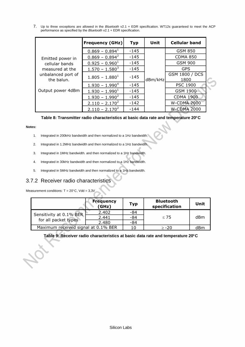
7. Up to three exceptions are allowed in the Bluetooth v2.1 + EDR specification. WT12s guaranteed to meet the ACP performance as specified by the Bluetooth v2.1 + EDR specification.
Frequency (GHz) Typ Unit Cellular band
0.869 – 0.8941 -145 GSM 850
0.869 – 0.8942 -145 CDMA 850
0.925 – 0.9601 -145 GSM 900
1.570 – 1.5803 -145 GPS
1.805 – 1.8801 -145
GSM 1800 / DCS
1800
1.930 – 1.9904 -145 PSC 1900
1.930 – 1.9901 -145 GSM 1900
1.930 – 1.9902 -145 CDMA 1900
2.110 – 2.1702 -142 W-CDMA 2000
2.110 – 2.1702 -144 W-CDMA 2000
Emitted power in
cellular bands
measured at the
unbalanced port of
the balun.
Output power 4dBm
dBm/kHz
Table 8: Transmitter radio characteristics at basic data rate and temperature 20C
Notes:
1. Integrated in 200kHz bandwidth and then normalized to a 1Hz bandwidth.
2. Integrated in 1.2MHz bandwidth and then normalized to a 1Hz bandwidth.
3. Integrated in 1MHz bandwidth. and then normalized to a 1Hz bandwidth.
4. Integrated in 30kHz bandwidth and then normalized to a 1Hz bandwidth.
5. Integrated in 5MHz bandwidth and then normalized to a 1Hz bandwidth.
3.7.2 Receiver radio characteristics
Measurement conditions: T = 20C, Vdd = 3,3V
Frequency
(GHz)Typ
Bluetooth
specificationUnit
2.402 -84
2.441 -84
2.480 -84
10 -20 dBm
Sensitivity at 0.1% BER
for all packet types
Maximum received signal at 0.1% BER
dBm 75
Table 9: Receiver radio characteristics at basic data rate and temperature 20C

Silicon Labs
Frequency
(GHz)Typ
Bluetooth
specificationUnit
30-2000 TBD -10
2000-2400 TBD -27
2500-3000 TBD -27
3000-3300 TBD -27
6 11 dB
-5 0 dB
-4 0 dB
-38 -30 dB
-23 -20 dB
-45 -40 dB
-44 -40 dB
-22 9 dB
-30 -39 dBmTBD - dBm/Hz
Adjacent channel selectivity C/I F=FImage1,2
Maximum level of intermodulation interferers3
Spurious output level4
dBm
Adjacent channel selectivity C/I F=F0 + 2 MHz1,2
Adjacent channel selectivity C/I F=F0 - 2 MHz1,2
Adjacent channel selectivity C/I F=F0 + 3 MHz1,2
Adjacent channel selectivity C/I F=F0 - 5 MHz1,2
Continuous power required to block
Bluetooth reception (for sensitivity of -
67dBm with 0.1% BER) measured at
the unbalanced port of the balun.C/I co-channel
Adjacent channel selectivity C/I F=F0 + 1MHz1,2
Adjacent channel selectivity C/I F=F0 - 1MHz1,2
Table 10: Receiver radio characteristics at basic data rate and temperature 20C
Notes:
1. Up to five exceptions are allowed in the Bluetooth v2.1 + EDR specification. BlueCore4 is guaranteed to meet the C/I performance as specified by the Bluetooth v2.1 + EDR specification.
2. Measured at F = 2441MHz
3. Measured at f1-f2 = 5MHz. Measurement is performed in accordance with Bluetooth RF test RCV/CA/05/c. i.e. wanted signal at -64dBm
4. Measured at the unbalanced port of the balun. Integrated in 100kHz bandwidth and then normalized to 1Hz. Actual figure is typically below TBD dBm/Hz except for peaks of -52dBm in band at 2.4GHz and d80dBm at 3.2GHz
Frequency
(GHz)Typ Unit Cellular band
0.824 – 0.849 2.0 GSM 850
0.824 – 0.849 TBD CDMA
0.880 – 0.915 5.0 GSM 900
1.710 – 1.785 4.0 GSM 1800 / DCS 1800
1.710 – 1.785 3.0 GSM 1900 / PCS 1900
1.850 – 1.910 TBD CDMA 1900
1.920 – 1.980 TBD W-CDMA 2000
0.824 – 0.849 -10 GSM 850
0.824 – 0.849 TBD CDMA
0.880 – 0.915 -10 GSM 900
1.710 – 1.785 -9 GSM 1800 / DCS 1800
1.850 – 1.910 -9 GSM 1900 / PCS 1900
1.850 – 1.910 TBD CDMA 1900
1.920 – 1.980 TBD W-CDMA 2000
Emitted power in cellular
bands required to block
Bluetooth reception (for
sensitivity of -67dBm with
0.1% BER) measured at the
unbalanced port of the
balun.Continuous power in cellular
bands required to block
Bluetooth reception (for
sensitivity of-72dBm with
0.1% BER) measured at the
unbalanced port of the
balun.
dBm
dBm
Table 11: Receiver radio characteristics at basic data rate and temperature 20C

Silicon Labs
3.8 Radio Characteristics – Enhanced Data Rate
3.8.1 Transmitter radio characteristics
Measurement conditions: T = 20C, Vdd = 3,3V
Typ Bluetooth specification Unit
+1 -6 to 42 dBm
-1 -4 to 1 dB
3 10 kHz
RMS DEV - 135 %
99% DEV - 205 %
Peak DEVM - 255 %
Modulation
accuracy3,4
Carrier frequency stability3
Relative transmit power3
Maximum output power1
Table 12: Transmitter radio characteristics at enhanced data rate and temperature 20C
Notes:
1. Results shown are referenced to input of the RF balun.
2. WT12 firmware maintains the transmit power to be within the Bluetooth v2.1 + EDR specification limits
3. Class 2 RF transmit power range, Bluetooth v2.1 + EDR specification
4. Measurements methods are in accordance with the EDR RF Test Specification v2.1.E.2
5. Modulation accuracy utilizes differential error vector magnitude (DEVM) with tracking of the carrier frequency drift.
6. The Bluetooth specification values are for 8DPSK modulation (values for the S/4 DQPSK modulation are less stringent)

Silicon Labs
3.8.2 Receiver radio characteristics
Measurement conditions: T = 20C, Vdd = 3,3V
Modulation TypBluetooth
specificationUnit
/4 DQPSK -87 -70
8DQPSK -79 -70
/4 DQPSK -7 -20
8DQPSK -7 -20
/4 DQPSK +11 13
8DQPSK +19 21
/4 DQPSK -8 0
8DQPSK -2 5
/4 DQPSK -8 0
8DQPSK -2 5
/4 DQPSK -35 -30
8DQPSK -35 -25
/4 DQPSK -23 -20
8DQPSK -19 -13
/4 DQPSK -43 -40
8DQPSK -40 -33
/4 DQPSK -43 -40
8DQPSK -38 -33
/4 DQPSK -17 -7
8DQPSK -11 0
C/I co-channel at 0.1% BER1
Adjacent channel selectivity
C/I F = F0 + 1MHz1,2,3
Adjacent channel selectivity
C/I F = F0 - 5MHz1,2,3
Adjacent channel selectivity
C/I F = FImage1,2,3
dBm
dB
Adjacent channel selectivity
C/I F = F0 - 1MHz1,2,3
Adjacent channel selectivity
C/I F=F0 + 2MHz1,2,3
Adjacent channel selectivity
C/I F = F0 - 2MHz1,2,3
Adjacent channel selectivity
C/I F = F0 + 3MHz1,2,3
Sensitivity at 0.1% BER for
all packet types1
Maximum received signal at
0.1% BER1
Table 13: Receiver radio characteristics at enhanced data rate and temperature 20C
Notes:
1. Results shown are referenced to input of the RF balun
2. Measurements methods are in accordance with the EDR RF Test Specification v2.1.E.2
3. Up to five exceptions are allowed in EDR RF Test Specification v2.1.E.2. WT12 is guaranteed to meet the C/I performance as specified by the EDR RF Test Specification v2.1.E.2.
4. Measured at F0 = 2405MHz, 2441MHz, 2477MHz
Silicon Labs
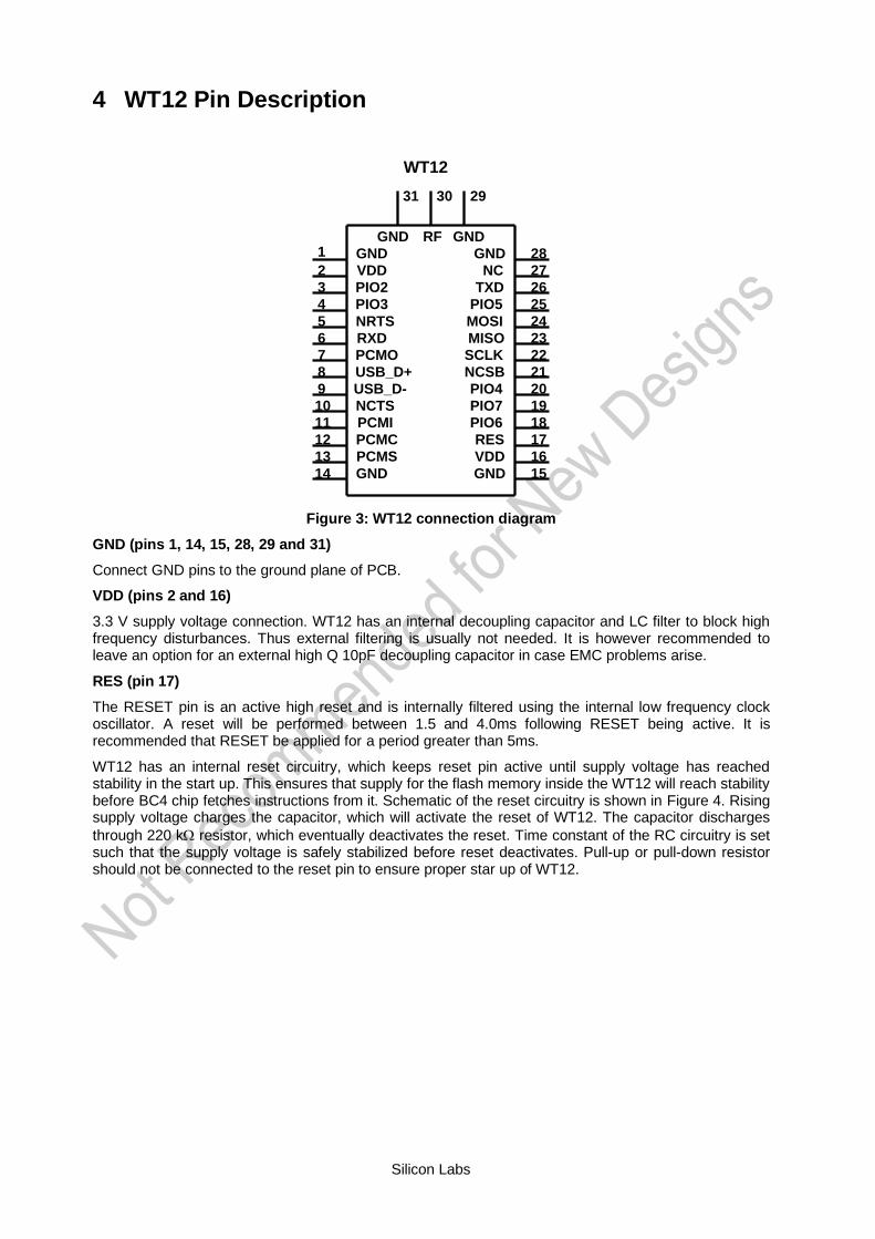
4 WT12 Pin Description
1
2
3
4
5
6
7
8
9
10
12
11
13
14
19
17
18
16
15
24
22
23
21
20
27
28
26
25
WT12
293031
GND
VDD
PIO2
PIO3
NRTS
RXD
PCMO
USB_D+
USB_D-
NCTS
PCMI
PCMC
PCMS
GND
GND
NC
TXD
PIO5
MOSI
MISO
SCLK
NCSB
PIO4
PIO7
PIO6
RES
VDD
GND
GND GNDRF
Figure 3: WT12 connection diagram
GND (pins 1, 14, 15, 28, 29 and 31)
Connect GND pins to the ground plane of PCB.
VDD (pins 2 and 16)
3.3 V supply voltage connection. WT12 has an internal decoupling capacitor and LC filter to block high frequency disturbances. Thus external filtering is usually not needed. It is however recommended to leave an option for an external high Q 10pF decoupling capacitor in case EMC problems arise.
RES (pin 17)
The RESET pin is an active high reset and is internally filtered using the internal low frequency clock oscillator. A reset will be performed between 1.5 and 4.0ms following RESET being active. It is recommended that RESET be applied for a period greater than 5ms.
WT12 has an internal reset circuitry, which keeps reset pin active until supply voltage has reached stability in the start up. This ensures that supply for the flash memory inside the WT12 will reach stability before BC4 chip fetches instructions from it. Schematic of the reset circuitry is shown in Figure 4. Rising supply voltage charges the capacitor, which will activate the reset of WT12. The capacitor discharges
through 220 k resistor, which eventually deactivates the reset. Time constant of the RC circuitry is set such that the supply voltage is safely stabilized before reset deactivates. Pull-up or pull-down resistor should not be connected to the reset pin to ensure proper star up of WT12.

Silicon Labs
Figure 4: WT12 internal reset circuitry
PIO2 – PIO7 (pins 3, 4, 18, 19, 20 and 25)
Programmable digital I/O lines. All PIO lines can be configured through software to have either weak or strong pull-ups or pull-downs. Configuration for each PIO line depends on the application. See section 10 “I/O parallel ports” for detailed descriptions for each terminal. Default configuration for all of the PIO lines is input with weak internal pull-down.
NC (pin 27)
This pin is internally connected to PIO1.
NRTS (pin 5)
CMOS output with weak internal pull-up. Can be used to implement RS232 hardware flow control where RTS (request to send) is active low indicator. UART interface requires external RS232 transceiver chip.
NCTS (pin 10)
CMOS input with weak internal pull-down. Can be used to implement RS232 hardware flow control where CTS (clear to send) is active low indicator. UART interface requires external RS232 transceiver chip.
RXD (pin 6)
CMOS input with weak internal pull-down. RXD is used to implement UART data transfer from another device to WT12. UART interface requires external RS232 transceiver chip.
TXD (pin 26)
CMOS output with weak internal pull-up. TXD is used to implement UART data transfer from WT12 to another device. UART interface requires external RS232 transceiver chip.
PCMO (pin 7)
CMOS output with weak internal pull-down. Used in PCM (pulse code modulation) interface to transmit digitized audio.
PCMI (pin 11)
CMOS input with weak internal pull-down. Used in PCM interface to receive digitized audio.
PCMC (pin 12)
Bi-directional synchronous data clock signal pin with weak internal pull-down. PCMC is used in PCM interface to transmit or receive CLK signal. When configured as a master, WT12 generates clock signal for the PCM interface. When configured as a slave PCMC is an input and receives the clock signal from another device.
PCMS (pin 13)
Bi-directional synchronous data strobe with weak internal pull-down. When configured as a master, WT12 generates SYNC signal for the PCM interface. When configured as a slave PCMS is an input and receives the SYNC signal from another device.

Silicon Labs
USB_D+ (pin 8)
Bi-directional USB data line with a selectable internal 1.5 k pull-up implemented as a current source (compliant with USB specification v1.2) External series resistor is required to match the connection to the characteristic impedance of the USB cable.
USB_D- (pin 9)
Bi-directional USB data line. External series resistor is required to match the connection to the characteristic impedance of the USB cable.
NCSB (pin 21)
CMOS input with weak internal pull-up. Active low chip select for SPI (serial peripheral interface).
SCLK (pin 22)
CMOS input for the SPI clock signal with weak internal pull-down. WT12 is the slave and receives the clock signal from the device operating as a master.
MISO (pin 23)
SPI data output with weak internal pull-down.
MOSI (pin 24)
SPI data input with weak internal pull-down.
RF (pin 30)
Connect external RF-transceiver antenna to this pin when chip antenna is not in use.
Silicon Labs
5 Physical Interfaces
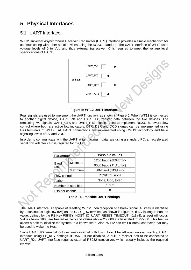
5.1 UART Interface
WT12 Universal Asynchronous Receiver Transmitter (UART) interface provides a simple mechanism for communicating with other serial devices using the RS232 standard. The UART interface of WT12 uses voltage levels of 0 to Vdd and thus external transceiver IC is required to meet the voltage level specifications of UART.
UART_TX
UART_RX
UART_RTS
UART_CTS
WT12
Figure 5: WT12 UART interface
Four signals are used to implement the UART function, as shown in Figure 5. When WT12 is connected to another digital device, UART_RX and UART_TX transfer data between the two devices. The remaining two signals, UART_CTS and UART_RTS, can be used to implement RS232 hardware flow control where both are active low indicators. DTR, DSR and DCD signals can be implemented using PIO terminals of WT12. All UART connections are implemented using CMOS technology and have signaling levels of 0V and VDD.
In order to communicate with the UART at its maximum data rate using a standard PC, an accelerated serial port adapter card is required for the PC.
Parameter Possible values
Baud rate
Minimum 1200 baud (≤2%Error)
9600 baud (≤1%Error)
Maximum 3.0Mbaud (≤1%Error)
Flow control RTS/CTS, none
Parity None, Odd, Even
Number of stop bits 1 or 2
Bits per channel 8
Table 14: Possible UART settings
The UART interface is capable of resetting WT12 upon reception of a break signal. A Break is identified by a continuous logic low (0V) on the UART_RX terminal, as shown in Figure 6. If tBRK is longer than the value, defined by the PS Key PSKEY_HOST_IO_UART_RESET_TIMEOUT, (0x1a4), a reset will occur. Values below 1000 are treated as zero and values above 255000 are truncated to 255000. This feature allows a host to initialize the system to a known state. Also, WT12 can emit a Break character that may be used to wake the Host.
Since UART_RX terminal includes weak internal pull-down, it can’t be left open unless disabling UART interface using PS_KEY settings. If UART is not disabled, a pull-up resistor has to be connected to UART_RX. UART interface requires external RS232 transceiver, which usually includes the required pull-up.

Silicon Labs
tBRKUART_RX
Figure 6: Break signal
Note:
Table 15 shows a list of commonly used Baud rates and their associated values for the Persistent Store Key PSKEY_UART_BAUD_RATE (0x204). There is no requirement to use these standard values. Any Baud rate within the supported range can be set in the Persistent Store Key according to the formula in Equation below.
Baud Rate =PSKEY_UART_BAUD_RATE
0.004096
Figure 7: Baud rate calculation formula
Hex Dec
1200 0x0005 5 1.73%2400 0x000a 10 1.73%4800 0x0014 20 1.73%9600 0x0027 39 -0.82%19200 0x004f 79 0.45%38400 0x009d 157 -0.18%57600 0x00ec 263 0.03%76800 0x013b 315 0.14%
115200 0x01d8 472 0.03%230400 0x03b0 944 0.03%460800 0x075f 1887 -0.02%921600 0x0ebf 3775 0.00%1382400 0x161e 5662 -0.01%1843200 0x1d7e 7550 0.00%
2765800 0x2c3d 11325 0.00%
Persistent store valuesBaud rate Error
Table 15: UART baud rates and error values
5.1.1 UART Configuration While RESET is Active
The UART interface for WT12 while the chip is being held in reset is tri-state. This will allow the user to daisy chain devices onto the physical UART bus. The constraint on this method is that any devices connected to this bus must tri-state when WT12reset is de-asserted and the firmware begins to run.
5.1.2 UART Bypass Mode
Alternatively, for devices that do not tri-state the UART bus, the UART bypass mode on WT12 can be used. The default state of WT12 after reset is de-asserted, this is for the host UART bus to be connected to the WT12 UART, thereby allowing communication to WT12 via the UART.
In order to apply the UART bypass mode, a BCCMD command will be issued to WT12 upon this, it will switch the bypass to PIO[7:4] as shown in Figure 8. Once the bypass mode has been invoked, WT12 will enter the deep sleep state indefinitely.
In order to re-establish communication with WT12, the chip must be reset so that the default configuration takes affect.

Silicon Labs
It is important for the host to ensure a clean Bluetooth disconnection of any active links before the bypass mode is invoked. Therefore it is not possible to have active Bluetooth links while operating the bypass mode.
The current consumption for a device in UART Bypass Mode is equal to the values quoted for a device in standby mode.
WT12
Hostprocessor
Testinterface
RXD
CTS
RTS
TXD
Anotherdevice
TX
RTS
CTS
RX
UART_TX
UART_RTS
UART_CTS
UART_RX
RESET
PIO5
PIO6
PIO7
PIO4
UART
Figure 8: UART bypass mode

Silicon Labs
5.2 USB Interface
WT12 USB devices contain a full speed (12Mbits/s) USB interface that is capable of driving a USB cable directly. No external USB transceiver is required. To match the connection to the characteristic impedance of the USB cable, series resistors must be included to both of the signal lines. These should be of 1% tolerance and the value required may vary between 0 and 20 ohm with 10 ohm being nominal. The resistors should be placed close to the USB pins of the module in order to avoid reflections. The module has internally 22 ohm resistors in series. The total input impedance seen by the cable is affected by the IC characteristics, track layout and the connector. The cable impedance is approximately 40 ohm.
The device operates as a USB peripheral, responding to requests from a master host controller such as a PC. Both the OHCI and the UHCI standards are supported. The set of USB endpoints implemented can behave as specified in the USB section of the Bluetooth v2.1 + EDR specification or alternatively can appear as a set of endpoint appropriate to USB audio devices such as speakers.
As USB is a Master/Slave oriented system (in common with other USB peripherals), WT12 only supports USB Slave operation.
5.2.1 USB Pull-Up Resistor
WT12 features an internal USB pull-up resistor. This pulls the USB_DP pin weakly high when WT12 is ready to enumerate. It signals to the PC that it is a full speed (12Mbit/s) USB device.
The USB internal pull-up is implemented as a current source, and is compliant with Section 7.1.5 of the USB specification v1.2. The internal pull-up pulls USB_D+ high to at least 2.8V when loaded with a
15k +/-5% pull-down resistor (in the hub/host). This presents a Therein resistance to the host of at
least 900. Alternatively, an external 1.5k pull-up resistor can be placed between a PIO line and D+ on the USB cable. The firmware must be alerted to which mode is used by setting PS Key PSKEY_USB_PIO_PULLUP appropriately. The default setting uses the internal pull-up resistor.
5.2.2 Self Powered Mode
In self powered mode, the circuit is powered from its own power supply and not from the VBUS (5V) line of the USB cable. It draws only a small leakage current (below 0.5mA) from VBUS on the USB cable. This is the easier mode for which to design for, as the design is not limited by the power that can be drawn from the USB hub or root port. However, it requires that VBUS be connected to WT12 via a voltage devider (Rvb1 and Rvb2), so WT12 can detect when VBUS is powered up. Voltage divider is essential to drop the 5V voltage at the VBUS to 3,3V expected at the USB interface of WT12. WT12 will not pull USB_DP high when VBUS is off.
Self powered USB designs (powered from a battery or PSU) must ensure that a PIO line is allocated for USB pull-up purposes. A 1.5K 5% pull-up resistor between USB_DP and the selected PIO line should be fitted to the design. Failure to fit this resistor may result in the design failing to be USB compliant in self powered mode. The internal pull-up in WT12 is only suitable for bus powered USB devices i.e. dongles.
PIO
USB_D+
USB_D-
USB_ON
R =1.5k
Rvb1
WT12
Rvb2
Figure 9: USB in self powered mode

Silicon Labs
The terminal marked USB_ON can be any free PIO pin. The PIO pin selected must be registered by setting PSKEY_USB_PIO_VBUS to the corresponding pin number. In self powered mode PSKEY_USB_PIO_PULLUP must be set to match with the PIO selected.
Note:
USB_ON is shared with WT12 PIO terminals (PIO2-PIO7).
5.2.3 Bus Powered Mode
In bus powered mode the application circuit draws its current from the 5V VBUS supply on the USB cable. WT12 negotiates with the PC during the USB enumeration stage about how much current it is allowed to consume.
For WT12 Bluetooth applications, it is recommended that the regulator used to derive 3.3V from VBUS is rated at 100mA average current and should be able to handle peaks of 120mA without fold back or limiting. In bus powered mode, WT12 requests 100mA during enumeration.
When selecting a regulator, be aware that VBUS may go as low as 4.4V. The inrush current (when charging reservoir and supply decoupling capacitors) is limited by the USB specification (see USB specification v1.1, Section 7.2.4.1). Some applications may require soft start circuitry to limit inrush current if more than 10pF is present between VBUS and GND.
The 5V VBUS line emerging from a PC is often electrically noisy. As well as regulation down to 3.3V, applications should include careful filtering of the 5V line to attenuate noise that is above the voltage regulator bandwidth.
In bus powered mode PSKEY_USB_PIO_PULLUP must be set to 16 for internal pull-up (default configuration in WT12).
USB_D+
USB_D-
USB_ON
Voltageregulator
WT12
VBUS
GND
Figure 10: USB in bus powered mode
5.2.4 Suspend Current
All USB devices must permit the USB controller to place them in a USB Suspend mode. While in USB Suspend, bus powered devices must not draw more than 0.5mA from USB VBUS (self powered devices may draw more than 0.5mA from their own supply). This current draw requirement prevents operation of the radio by bus powered devices during USB Suspend.
The voltage regulator circuit itself should draw only a small quiescent current (typically less than 100uA) to ensure adherence to the suspend current requirement of the USB specification. This is not normally a problem with modern regulators. Ensure that external LEDs and/or amplifiers can be turned off by WT12. The entire circuit must be able to enter the suspend mode. (For more details on USB Suspend, see separate CSR documentation).
5.2.5 Detach and Wake-Up Signaling
WT12 can provide out-of-band signaling to a host controller by using the control lines called ‘USB_DETACH’ and ‘USB_WAKE_UP’. These are outside the USB specification (no wires exist for them inside the USB cable), but can be useful when embedding WT12 into a circuit where no external USB is visible to the user. Both control lines are shared with PIO pins and can be assigned to any PIO

Silicon Labs
pin by setting the PS Keys PSKEY_USB_PIO_DETACH and PSKEY_USB_PIO_WAKEUP to the selected PIO number.
USB_DETACH is an input which, when asserted high, causes WT12 to put USB_D- and USB_D+ in high impedance state and turned off the pull-up resistor on D+. This detaches the device from the bus and is logically equivalent to unplugging the device. When USB_DETACH is taken low, WT12 will connect back to USB and await enumeration by the USB host.
USB_WAKE_UP is an active high output (used only when USB_DETACH is active) to wake up the host and allow USB communication to recommence. It replaces the function of the software USB WAKE_UP message (which runs over the USB cable), and cannot be sent while WT12 is effectively disconnected from the bus.
USB_WAKE_UP
USB_DETACH
Port_ImbedanceUSB_DPUSB_DNUSB_PULL_UP
10ms max
10ms max10ms max
No max
Disconnected
Figure 11: USB_DETACH and USB_WAKE_UP Signal
5.2.6 USB Driver
A USB Bluetooth device driver is required to provide a software interface between WT12 and Bluetooth software running on the host computer. Suitable drivers are available from www.silabs.com .
5.2.7 USB 1.1 Compliance
WT12 is qualified to the USB specification v1.1, details of which are available from http://www.usb.org. The specification contains valuable information on aspects such as PCB track impedance, supply inrush current and product labeling.
Although WT12 meets the USB specification, Silicon Laboratories cannot guarantee that an application circuit designed around the module is USB compliant. The choice of application circuit, component choice and PCB layout all affect USB signal quality and electrical characteristics. The information in this document is intended as a guide and should be read in association with the USB specification, with particular attention being given to Chapter 7. Independent USB qualification must be sought before an application is deemed USB compliant and can bear the USB logo. Such qualification can be obtained from a USB plug fest or from an independent USB test house.
Terminals USB_D+ and USB_D- adhere to the USB specification 2.0 (Chapter 7) electrical requirements.
5.2.8 USB 2.0 Compatibility
WT12 is compatible with USB v2.0 host controllers; under these circumstances the two ends agree the mutually acceptable rate of 12Mbits/s according to the USB v2.0 specification.

Silicon Labs
5.3 SPI Interface
The synchronous serial port interface (SPI) is for interfacing with other digital devices. The SPI port can be used for system debugging. It can also be used for programming the Flash memory. SPI interface is connected using the MOSI, MISO, CSB and CLK pins.
The module operates as a slave and thus MISO is an output of the module. MISO is not in high-impedance state when CSB is pulled high. Instead, the module outputs 0 if the processor is running and 1 if it is stopped. Thus WT12 should not be connected in a multi-slave arrangement by simple parallel connection of slave MISO lines.
The SPI interface cannot be used for application purposes, but is dedicated for debugging and firmware updates.

Silicon Labs
5.4 PCM Interface
Pulse Code Modulation (PCM) is a standard method used to digitize audio (particularly voice) patterns for transmission over digital communication channels. Through its PCM interface, WT12 has hardware support for continual transmission and reception of PCM data, thus reducing processor overhead for wireless headset applications. WT12 offers a bi directional digital audio interface that routes directly into the baseband layer of the on chip firmware. It does not pass through the HCI protocol layer.
Hardware on WT12 allows the data to be sent to and received from a SCO connection. Up to three SCO connections can be supported by the PCM interface at any one time.
WT12 can operate as the PCM interface Master generating an output clock of 128, 256 or 512kHz. When configured as PCM interface slave it can operate with an input clock up to 2048kHz. WT12 is compatible with a variety of clock formats, including Long Frame Sync, Short Frame Sync and GCI timing environments.
It supports 13 or 16-bit linear, 8-bit -law or A-law companded sample formats at 8ksamples/s and can receive and transmit on any selection of three of the first four slots following PCM_SYNC. The PCM configuration options are enabled by setting the PS Key PS KEY_PCM_CONFIG32 (0x1b3). WT12 interfaces directly to PCM audio devices including the following:
• Qualcomm MSM 3000 series and MSM 5000 series CDMA baseband devices
• OKI MSM7705 four channel A-law and -law CODEC
• Motorola MC145481 8-bit A-law and -law CODEC
• Motorola MC145483 13-bit linear CODEC
• STW 5093 and 5094 14-bit linear CODECs
• BlueCore4-External is also compatible with the Motorola SSI™ interface
5.4.1 PCM Interface Master/Slave
When configured as the Master of the PCM interface, WT12 generates PCM_CLK and PCM_SYNC.
PCM_OUT
PCM_IN
PCM_CLK
PCM_SYNC 8kHz
128/256/512 kHz
WT12
Figure 12: WT12 as PCM master
When configured as the Slave of the PCM interface, WT12 accepts PCM_CLK and PCM_SYNC. PCM_CLK rates up to 2048kHz are accepted.

Silicon Labs
PCM_OUT
PCM_IN
PCM_CLK
PCM_SYNC 8kHz
Up to 2048kHz
WT12
Figure 13: WT12 as PCM slave
5.4.2 Long Frame Sync
Long Frame Sync is the name given to a clocking format that controls the transfer of PCM data words or samples. In Long Frame Sync, the rising edge of PCM_SYNC indicates the start of the PCM word. When WT12 is configured as PCM Master, generating PCM_SYNC and PCM_CLK, then PCM_SYNC is 8-bits long. When BlueCore4-External is configured as PCM Slave, PCM_SYNC may be from two
consecutive falling edges of PCM_CLK to half the PCM_SYNC rate, i.e. 62.5s long.
WT12 samples PCM_IN on the falling edge of PCM_CLK and transmits PCM_OUT on the rising edge. PCM_OUT may be configured to be high impedance on the falling edge of PCM_CLK in the LSB position or on the rising edge.
1 2 3 4 5 6 7 8PCM_OUT
PCM_CLK
PCM_SYNC
1 2 3 4 5 6 7 8undefined undefinedPCM_IN
Figure 14: Long frame sync (shown with 8-bit Companded Sample)
5.4.3 Short Frame Sync
In Short Frame Sync the falling edge of PCM_SYNC indicates the start of the PCM word. PCM_SYNC is always one clock cycle long.
1 2 3 4 5 6 7 8PCM_OUT
PCM_CLK
PCM_SYNC
1 2 3 4 5 6 7 8undefinedPCM_IN
9 10 11 12 13 14 15 16
9 10 11 12 13 14 15 16 undefined
Figure 15: Short frame sync (shown with 16-bit Companded Sample)

Silicon Labs
As with Long Frame Sync, WT12 samples PCM_IN on the falling edge of PCM_CLK and transmits PCM_OUT on the rising edge. PCM_OUT may be configured to be high impedance on the falling edge of PCM_CLK in the LSB position or on the rising edge.
5.4.4 Multi Slot Operation
More than one SCO connection over the PCM interface is supported using multiple slots. Up to three SCO connections can be carried over any of the first four slots.
1 2 3 4 5 6 7 8PCM_OUT
PCM_CLK
LONG_PCM_SYNC
1 2 3 4 5 6 7 8undefined undefinedPCM_IN
SHORT_PCM_SYNC
OR
Figure 16: Multi Slot Operation with Two Slots and 8-bit Companded Samples
5.4.5 GCI Interface
WT12 is compatible with the General Circuit Interface, a standard synchronous 2B+D ISDN timing interface. The two 64Kbps B channels can be accessed when this mode is configured.
1 2 3 4 5 6 7 8PCM_OUT
PCM_CLK
PCM_SYNC
1 2 3 4 5 6 7 8undefinedPCM_IN
1 2 3 4 5 6 7 8
1 2 3 4 5 6 7 8 undefined
Figure 17: GCI Interface
The start of frame is indicated by the rising edge of PCM_SYNC and runs at 8kHz. With WT12 in Slave mode, the frequency of PCM_CLK can be up to 4.096MHz.
5.4.6 Slots and Sample Formats
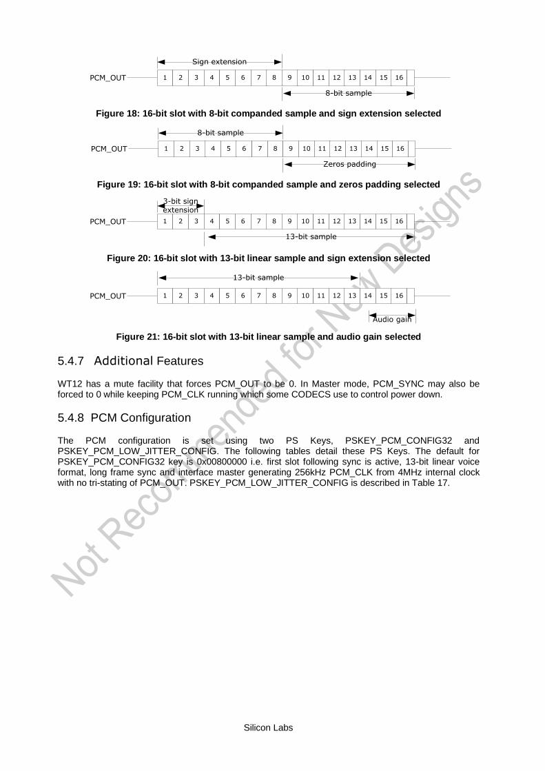
WT12 can receive and transmit on any selection of the first four slots following each sync pulse. Slot durations can be either 8 or 16 clock cycles. Duration’s of 8 clock cycles may only be used with 8-bit sample formats. Durations of 16 clocks may be used with 8, 13 or 16-bit sample formats.
WT12 supports 13-bit linear, 16-bit linear and 8-bit -law or A-law sample formats. The sample rate is 8ksamples/s. The bit order may be little or big Endian. When 16-bit slots are used, the 3 or 8 unused bits in each slot may be filled with sign extension, padded with zeros or a programmable 3-bit audio attenuation compatible with some Motorola CODECs.
Silicon Labs
PCM_OUT 1 2 3 4 5 6 7 8 9 10 11 12 13 14 15 16
Sign extension
8-bit sample
Figure 18: 16-bit slot with 8-bit companded sample and sign extension selected
PCM_OUT 1 2 3 4 5 6 7 8 9 10 11 12 13 14 15 16
8-bit sample
Zeros padding
Figure 19: 16-bit slot with 8-bit companded sample and zeros padding selected
PCM_OUT 1 2 3 4 5 6 7 8 9 10 11 12 13 14 15 16
3-bit signextension
13-bit sample
Figure 20: 16-bit slot with 13-bit linear sample and sign extension selected
PCM_OUT 1 2 3 4 5 6 7 8 9 10 11 12 13 14 15 16
Audio gain
13-bit sample
Figure 21: 16-bit slot with 13-bit linear sample and audio gain selected
5.4.7 Additional Features
WT12 has a mute facility that forces PCM_OUT to be 0. In Master mode, PCM_SYNC may also be forced to 0 while keeping PCM_CLK running which some CODECS use to control power down.
5.4.8 PCM Configuration
The PCM configuration is set using two PS Keys, PSKEY_PCM_CONFIG32 and PSKEY_PCM_LOW_JITTER_CONFIG. The following tables detail these PS Keys. The default for PSKEY_PCM_CONFIG32 key is 0x00800000 i.e. first slot following sync is active, 13-bit linear voice format, long frame sync and interface master generating 256kHz PCM_CLK from 4MHz internal clock with no tri-stating of PCM_OUT. PSKEY_PCM_LOW_JITTER_CONFIG is described in Table 17.

Silicon Labs
Name Bit position Description
- 0 Set to 0
SLAVE MODE EN 1
0 selects Master mode with internal generation of PCM_CLK and
PCM_SYNC. 1 selects Slave mode requiring externally generated
PCM_CLK and PCM_SYNC. This should be set to 1 if
48M_PCM_CLK_GEN_EN (bit 11) is set.
SHORT SYNC EN 20 selects long frame sync (rising edge indicates start of frame), 1
selects short frame sync (falling edge indicates start of frame).
- 3 Set to 0
SIGN EXTENDED
EN4
0 selects padding of 8 or 13-bit voice sample into a 16- bit slot by
inserting extra LSBs, 1 selects sign extension. When padding is
selected with 3-bit voice sample, the 3 padding bits are the audio gain
setting; with 8-bit samples the 8 padding bits are zeroes.
LSB FIRST EN 5 0 transmits and receives voice samples MSB first, 1 uses LSB first.
TX TRISTATE EN 6
0 drives PCM_OUT continuously, 1 tri-states PCM_OUT immediately
after the falling edge of PCM_CLK in the last bit of an active slot,
assuming the next slot is not active.
TX TRISTATE
RISING EDGE EN7
0 tristates PCM_OUT immediately after the falling edge of PCM_CLK
in the last bit of an active slot, assuming the next slot is also not active.
1 tristates PCM_OUT after the rising edge of PCM_CLK.
SYNC SUPPRESS
EN8
0 enables PCM_SYNC output when master, 1 suppresses PCM_SYNC
whilst keeping PCM_CLK running. Some CODECS utilize this to enter
a low power state.
GCI MODE EN 9 1 enables GCI mode.
MUTE EN 10 1 forces PCM_OUT to 0.
48M PCM CLK GEN
EN11
0 sets PCM_CLK and PCM_SYNC generation via DDS from internal 4
MHz clock, as for BlueCore4-External. 1 sets PCM_CLK and
PCM_SYNC generation via DDS from internal 48 MHz clock.
LONG LENGTH
SYNC EN12
0 sets PCM_SYNC length to 8 PCM_CLK cycles and 1 sets length to
16 PCM_CLK cycles. Only applies for long frame sync and with
48M_PCM_CLK_GEN_EN set to 1.
- [20:16] Set to 0b00000.
MASTER CLK RATE [22:21]Selects 128 (0b01), 256 (0b00), 512 (0b10) kHz PCM_CLK frequency
when master and 48M_PCM_CLK_GEN_EN (bit 11) is low.
ACTIVE SLOT [26:23] Default is 0001. Ignored by firmaware
SAMPLE_FORMAT [28:27] Selects between 13 (0b00), 16 (0b01), 8 (0b10) bit sample with 16
cycle slot duration 8 (0b11) bit sample 8 cycle slot duration.
Table 16: PSKEY_PCM_CONFIG32 description
Name Bit position Description
CNT LIMIT [12:0] Sets PCM_CLK counter limit
CNT RATE [23:16] Sets PCM_CLK count rate.
SYNC LIMIT [31:24] Sets PCM_SYNC division relative to PCM_CLK.
Table 17: PSKEY_PCM_LOW_JITTER_CONFIG Description

6 I/O Parallel Ports
The Parallel Input Output (PIO) Port is a general-purpose I/O interface to WT12. The port consists of six programmable, bi-directional I/O lines, PIO[2:7]. Programmable I/O lines can be accessed either via an embedded application running on WT12 or via private channel or manufacturer-specific HCI commands.
All PIO lines are configured as inputs with weak pull downs at reset.
PIO[2] / USB_PULL_UP (1)
The function depends on whether WT12 is a USB or UART capable version. On UART versions, this terminal is a programmable I/O. On USB versions, it can drive a pull-up resistor on USB_D+. For application using external RAM this terminal may be programmed for chip select.
PIO[3] / USB_WAKE_UP (1)
On UART versions of WT12 this terminal is a programmable I/O. On USB versions, its function is selected by setting the Persistent Store Key PSKEY_USB_PIO_WAKEUP (0x2cf) either as a programmable I/O or as a USB_WAKE_UP function.
PIO[4] / USB_ON (1)
On UART versions of WT12 this terminal is a programmable I/O. On USB versions, the USB_ON function is also selectable.
PIO[5] / USB_DETACH (1)
On UART versions of WT12 this terminal is a programmable I/O. On USB versions, the USB_DETACH function is also selectable.
PIO[6] / CLK_REQ
Function is determined by Persistent Store Keys. Using PSKEY_CLOCK_REQUEST_ENABLE, (0x246) this terminal can be configured to be low when WT12 is in deep sleep and high when a clock is required. The clock must be supplied within 4ms of the rising edge of PIO[6] to avoid losing timing accuracy in certain Bluetooth operating modes.
PIO[7]
Programmable I/O terminal.
Silicon Labs
7 Software Stacks
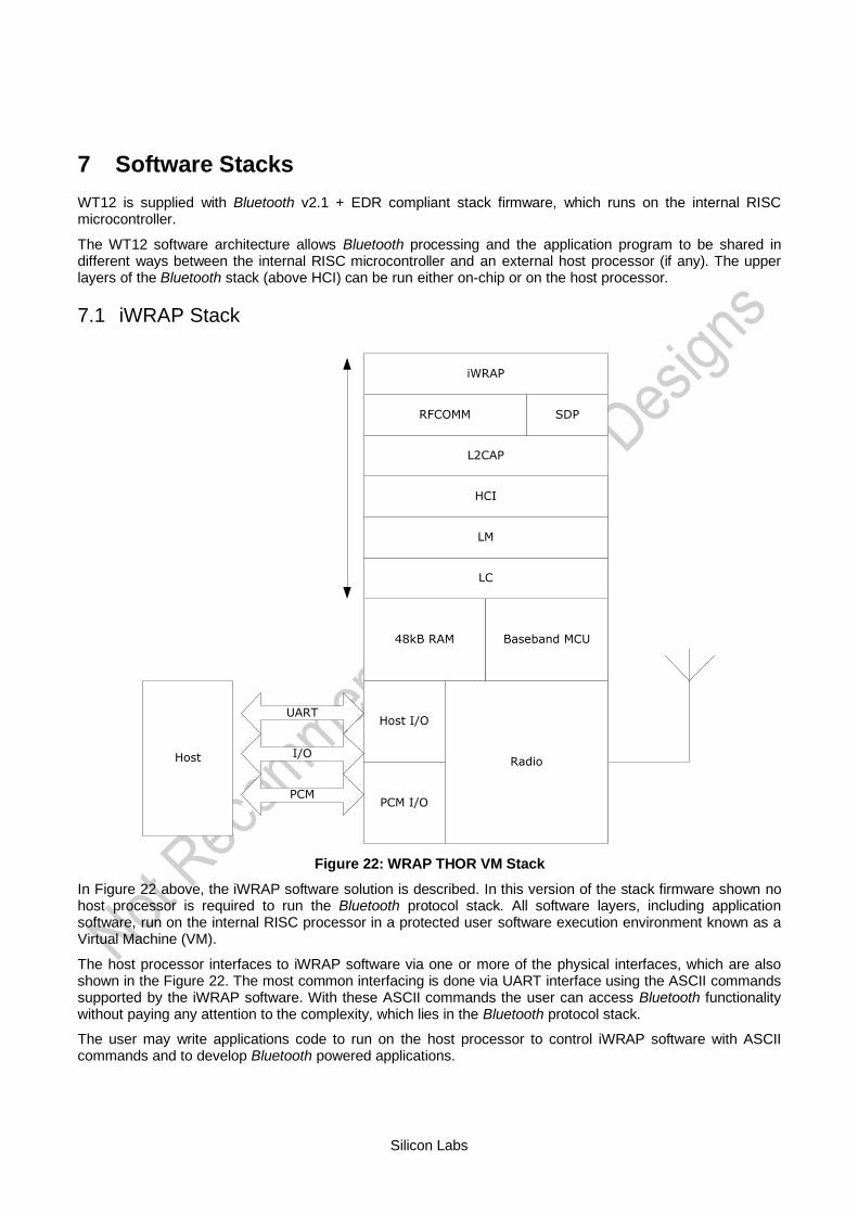
WT12 is supplied with Bluetooth v2.1 + EDR compliant stack firmware, which runs on the internal RISC microcontroller.
The WT12 software architecture allows Bluetooth processing and the application program to be shared in different ways between the internal RISC microcontroller and an external host processor (if any). The upper layers of the Bluetooth stack (above HCI) can be run either on-chip or on the host processor.
7.1 iWRAP Stack
PCM I/O
Host I/O
Radio
48kB RAM Baseband MCU
LC
LM
HCI
L2CAP
RFCOMM SDP
iWRAP
UART
Host I/O
PCM
Figure 22: WRAP THOR VM Stack
In Figure 22 above, the iWRAP software solution is described. In this version of the stack firmware shown no host processor is required to run the Bluetooth protocol stack. All software layers, including application software, run on the internal RISC processor in a protected user software execution environment known as a Virtual Machine (VM).
The host processor interfaces to iWRAP software via one or more of the physical interfaces, which are also shown in the Figure 22. The most common interfacing is done via UART interface using the ASCII commands supported by the iWRAP software. With these ASCII commands the user can access Bluetooth functionality without paying any attention to the complexity, which lies in the Bluetooth protocol stack.
The user may write applications code to run on the host processor to control iWRAP software with ASCII commands and to develop Bluetooth powered applications.
Silicon Labs
7.2 HCI Stack
PCM I/O
Host I/O
Radio
48kB RAM Baseband MCU
LC
LM
HCI
UART
USB
Host
I/O
PCM
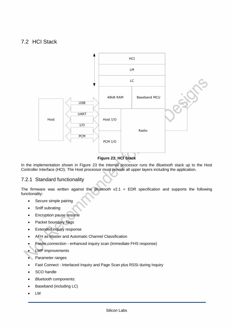
Figure 23: HCI Stack
In the implementation shown in Figure 23 the internal processor runs the Bluetooth stack up to the Host Controller Interface (HCI). The Host processor must provide all upper layers including the application.
7.2.1 Standard functionality
The firmware was written against the Bluetooth v2.1 + EDR specification and supports the following functionality:
• Secure simple pairing
• Sniff subrating
• Encryption pause resume
• Packet boundary flags
• Extended inquiry response
• AFH as Master and Automatic Channel Classification
• Faster connection - enhanced inquiry scan (immediate FHS response)
• LMP improvements
• Parameter ranges
• Fast Connect - Interlaced Inquiry and Page Scan plus RSSI during Inquiry
• SCO handle
• Bluetooth components:
• Baseband (including LC)
• LM
Silicon Labs
• HCI
• Standard UART and USB HCI Transport Layers
• All standard Bluetooth radio packet types
• Full Bluetooth data rate, enhanced data rates of 2 and 3Mbps. This is the maximum allowed by
• Operation with up to seven active ACL links
• Scatternet v2.5 operation
• eSCO
• Operation with up to three SCO or eSCO links routed to one or more remote devices (dependent on the parameters requested by the host, for example, to have three HV3 SCO links, all the links must go to slave devices)
• All standard SCO voice coding including transparent SCO
• Standard operating modes: Page, Inquiry, Page-Scan and Inquiry-Scan
• All standard pairing, authentication, link key and encryption operations
• Standard Bluetooth power saving mechanisms: Hold, Sniff and Park modes, including Forced Hold
• Dynamic control of peers' transmit power via LMP
• Master/Slave switch
• Broadcast
• Channel quality driven data rate
• All standard Bluetooth test modes
• EDR

Silicon Labs
7.2.2 Extra functionality:
The release extends the standard Bluetooth functionality with the following features:
• Support for BCSP, a proprietary, reliable alternative to the standard Bluetooth UART Host Transport (H4)
o A set of manufacturer-specific HCI extension commands, called BCCMDs, which provide:
o Access to the IC’s general-purpose PIO port
o Negotiated effective encryption key length on established Bluetooth links
o Access to the firmware’s random number generator
o Controls to set the default and maximum transmit powers; helping to reduce interference between overlapping, fixed-location piconets
o UART configuration
o Radio transmitter enable/disable; using a simple command to connect to a dedicated hardware switch that determines whether the radio can transmit
o Control of audio routing
• The firmware can read the voltage on several of the IC’s external pins. This is normally used to build a battery monitor, using either VM or host code (BlueCore4-Audio Flash can also read the battery voltage internally).
• The firmware provides support using VM to control the on-chip Battery Charger hardware for those Ics that provide this functionality
• A block of BCCMDs provides access to the IC’s PS configuration database. The database holds the device’s Bluetooth address, Class of Device, radio (transmit class) configuration, SCO routing, LM and USB constants, etc.
• A UART break condition can be used in three ways:
o Presenting a UART break condition to the IC can force the IC to perform a hardware reboot
o Presenting a break condition at boot time can hold the IC in a low power state, preventing normal initialisation while the condition exists
o With BCSP, the firmware can be configured to assert a break condition to the host before sending data; normally used to wake the host from a Deep Sleep state
• The DFU v1.0 standard has been extended with public/private key authentication, allowing manufacturers to control the firmware that can be loaded onto their Bluetooth modules
• A modified version of the DFU v1.0 protocol allows firmware upgrade via the IC’s UART
• A block of “radio test” or BIST commands allows direct control of the IC’s radio. This aids the development of modules’ radio designs, and can be used to support Bluetooth qualification.
• The firmware provides the VM environment in which to run application-specific code. Although the VM is mainly used with BlueLab, the VM can be used with this build, configured to act as an HCI device, to perform simple tasks such as flashing LEDs via the IC’s PIO port.
• Hardware low power modes: Shallow Sleep and Deep Sleep. The IC drops into modes that significantly reduce power consumption when the software goes idle.
• Support for eSCO connections at both HCI and RFCOMM levels
• SCO and eSCO channels are normally routed over HCI (over BCSP). However, up to three SCO/eSCO channels can be routed over the IC’s single PCM port (at the same time as routing any other SCO/eSCO channels over HCI). One SCO/eSCO link can be routed over the internal codec.
Silicon Labs
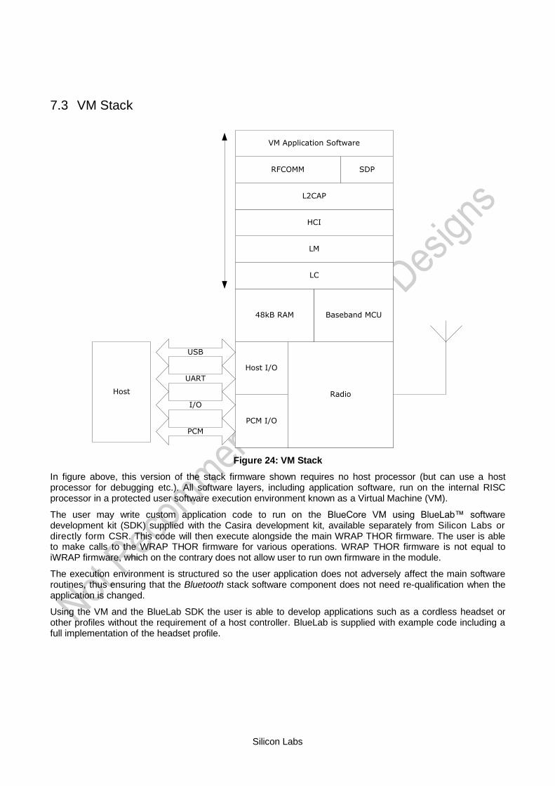
7.3 VM Stack
PCM I/O
Host I/O
Radio
48kB RAM Baseband MCU
LC
LM
HCI
L2CAP
RFCOMM SDP
VM Application Software
UART
USB
Host
I/O
PCM
Figure 24: VM Stack
In figure above, this version of the stack firmware shown requires no host processor (but can use a host processor for debugging etc.). All software layers, including application software, run on the internal RISC processor in a protected user software execution environment known as a Virtual Machine (VM).
The user may write custom application code to run on the BlueCore VM using BlueLab™ software development kit (SDK) supplied with the Casira development kit, available separately from Silicon Labs or directly form CSR. This code will then execute alongside the main WRAP THOR firmware. The user is able to make calls to the WRAP THOR firmware for various operations. WRAP THOR firmware is not equal to iWRAP firmware, which on the contrary does not allow user to run own firmware in the module.
The execution environment is structured so the user application does not adversely affect the main software routines, thus ensuring that the Bluetooth stack software component does not need re-qualification when the application is changed.
Using the VM and the BlueLab SDK the user is able to develop applications such as a cordless headset or other profiles without the requirement of a host controller. BlueLab is supplied with example code including a full implementation of the headset profile.

Silicon Labs
Notes:
Sample applications to control PIO lines can also be written with BlueLab SDK and the VM for the HCI stack.
7.4 Software Development
WT12 Evaluation Kits are available to allow the evaluation of the WT12 hardware and software as well CSR BlueLab toolkit for developing on-chip and host software.

Silicon Labs
8 Enhanced Data Rate
EDR has been introduced to provide 2x and optionally 3x data rates with minimal disruption to higher layers of the Bluetooth stack. CSR supports both of the new data rates, with WT12. WT12 is compliant with revision v2.0.E.2 of the specification.
8.1 Enhanced Data Rate Baseband
At the baseband level EDR uses the same 1.6kHz slot rate as basic data rate and therefore the packets can be 1, 3, or 5 slots long as per the basic data rate. Where EDR differs from the basic data rate is that in the same 1MHz symbol rate 2 or 3bits are used per symbol, compared to 1bit per symbol used by the basic data rate. To achieve the increase in number of bits symbol, two new modulation schemes have been introduced as summarized in Table 18 presented below and the modulation schemes are explained in the further sections.
Scheme Bits per symbol Modulation
Basic data rate 1 GFSK
Enhanced data rate 2 P/4 DQPSK
Enhanced data rate 3 8DPSK (optional)
Table 18: Data rate schemes
Although the EDR uses new packets Link establishment and management are unchanged and still use Basic Rate packets.
8.2 Enhanced Data Rate π/4 DQPSK
4-state Differential Phase Shift Keying
2 bits determine phase shift between consecutive symbols
2 bits determine phase shift between consecutive symbols
S/4 rotation avoids phase shift of S, which would cause large amplitude variation
Raised Cosine pulse shaping filter to further reduce side band emissions
Bit pattern Phase shift
00
01
10 −
11 −
Table 19: 2 bits determine phase shift between consecutive symbols
8.3 8DQPSK
8-state Differential Phase-Shift Keying
Three bits determine phase shift between consecutive symbols.

Silicon Labs
Bit pattern Phase shift
−
−
−
Table 20: 3 bits determine phase shift between consecutive symbols
Figure 25: 8DQPSK

Silicon Labs
9 Layout and Soldering Considerations
9.1 Soldering recommendations
WT12 is compatible with industrial standard reflow profile for Pb-free solders. The reflow profile used is dependent on the thermal mass of the entire populated PCB, heat transfer efficiency of the oven and particular type of solder paste used. Consult the datasheet of particular solder paste for profile configurations.
Silicon Laboratories will give following recommendations for soldering the module to ensure reliable solder joint and operation of the module after soldering. Since the profile used is process and layout dependent, the optimum profile should be studied case by case. Thus following recommendation should be taken as a starting point guide.
• Refer to technical documentations of particular solder paste for profile configurations
• Avoid using more than one flow.
• Reliability of the solder joint and self-alignment of the component are dependent on the solder volume. Minimum of 150m stencil thickness is recommended.
• Aperture size of the stencil should be 1:1 with the pad size.
• A low residue, “no clean” solder paste should be used due to low mounted height of the component.
9.2 Layout guidelines
It is strongly recommended to use good layout practices to ensure proper operation of the module. Placing copper or any metal near antenna deteriorates its operation by having effect on the matching properties. Metal shield around the antenna will prevent the radiation and thus metal case should not be used with the module. Use grounding vias separated max 3 mm apart at the edge of grounding areas to prevent RF penetrating inside the PCB and causing an unintentional resonator. Use GND vias all around the PCB edges. Figure 26 illustrates recommended PCB design around the antenna of WT12 when the module is placed at the edge of a PCB.
Do not place copper on the top layer under the module, as shown in Figure 26. The module has vias on the area shown, which can cause short circuit if there is copper underneath. Any metal placed closer than 20 mm in any direction from the antenna changes the matching properties and thus will considerably deteriorate the RF performance of the module.

Silicon Labs
Figure 26: Suggested PCB design around ACX antenna with the module at the edge of PCB
Following recommendations helps to avoid EMC problems arising in the design. Note that each design is unique and the following list do not consider all basic design rules such as avoiding capacitive coupling between signal lines. Following list is aimed to avoid EMC problems caused by RF part of the module. Use good consideration to avoid problems arising from digital signals in the design.
• Do not remove copper from the PCB more than needed. Use ground filling as much as possible. However remove small floating islands after copper pour.
• Do not place a ground plane underneath the antenna. The grounding areas under the module should be designed as shown in Figure 26.
• Use conductive vias separated max. 3 mm apart at the edge of the ground areas. This prevents RF to penetrate inside the PCB. Use ground vias extensively all over the PCB. If you allow RF freely inside the PCB, you have a potential resonator in your hand. All the traces in (and on) the PCB are potential antennas.
• Avoid loops.

Silicon Labs
• Ensure that signal lines have return paths as short as possible. For example if a signal goes to an inner layer through a via, always use ground vias around it. Locate them
tightly and symmetrically around the signal vias.
• Routing of any sensitive signals should be done in the inner layers of the PCB.
• Sensitive traces should have a ground area above and under the line. If this is not possible make sure that the return path is short by other means (for example using a ground line next to the signal line).

Silicon Labs
10 WT12 physical dimensions
20.0 mm
25.6 mm
0.6 mm
14.0 mm
10.0 mm
B l u e gi g a
5.0 mm
2.4 mm 2.0 mm
Tolerance for all the dimensions +/- 0.2 mm
Figure 27: WT12 dimensions
Figure 28: WT12 foot print

Silicon Labs
Figure 29: WT12 recommended PCB land pattern
Figure 30: WT12 pad dimensions

Silicon Labs
11 Package
bluegiga RoHS label
A
product
Label
1.0
W2
Reel Configuration and Production Label
D
BC
W1
RoHS Compliant
T E C H N O L O G I E S
Figure 31: Reel information
0.1M
ax
37.5±0.2
Figure 32: Cover tape spec

Silicon Labs
⚫◼
◼⬧◼⬧
P/N
3500275600
¡ Ó0.1
T
2.5
¡ Ó0.1¡ Ó0.1 ¡ Ó0.3 +0.1 ¡ Ó0.1 ¡ Ó0.1¡ Ó0.1 ¡ Ó0.1
25.914.4 20.244
BA W F
2.04.01.75 20.0
E P0 P1 P2
+0.1-0.0
VACANT
W
A
?1.5
20 PCS
start
Package direction:
VACANTquantity/500pcs
p1
F
T
p2A
B
B
Deta
il B
-B
p0
EB
20PCS
WT
12
WT
12
WT
12
WT
12
End of tape
Figure 33: Tape information
Dimensions
Tolerance

Silicon Labs
12 Package Marking
Figure 34: WT12-A Package marking
Line 1 Marking website www.silabs.com
Line 2 Marking Model WT12-A
Line 3 Marking FCC ID QOQWT12
Line 4 Marking IC ID 5123A-BGTWT 12A
Line 5 Marking KCC ID KCC-CRM-BGT-WT 12-A
Line 6 Marking Anatel ID 1233-16-3402
Line 7 Marking Japan ID 209-J0036
Line 8 Marking YYWWRMTT YY Last digit of Year (e.g.: 16 for 2016)
WW Work Week (01-53)
R Major Revision (fixed character 1-9, A-Z, assigned by Silicon Labs)
M Contract Manufacturer Site assigned by Silicon Labs
TT Unique Batch ID assigned by CM (2 characters A-Z)
Silicon Labs
13 Certifications
WT12 is compliant to the following specifications.
13.1 Bluetooth
WT12 module is qualified as a Bluetooth controller subsystem and it fullfills all the mandatory requirements of Bluetooth 2.1 + EDR core spesification. If not modified in any way, it is a complete Bluetooth entity, containing software and hardware functionality as well as the whole RF-part including the antenna. This practically translates to that if the module is used without modification of any kind, it does not need any Bluetooth approval work for evaluation on what needs to be tested.
WT12 qualified listing details:
https://www.Bluetooth.org/tpg/QLI_viewQDL.cfm?qid=17400
WT12 PICS details:
https://www.Bluetooth.org/tpg/showCorePICS.cfm?3A000A5A005C5043555E54
WT12 Qualified Design ID (QDID):
https://www.Bluetooth.org/tpg/QLI_viewQDL.cfm?qid=17400
13.2 FCC and IC
This device complies with Part 15 of the FCC Rules. Operation is subject to the following two conditions:
(1) this device may not cause harmful interference, and
(2) this device must accept any interference received, including interference that may cause undesired operation.
FCC RF Radiation Exposure Statement:
This equipment complies with FCC radiation exposure limits set forth for an uncontrolled environment. End users must follow the specific operating instructions for satisfying RF exposure compliance. This transmitter must not be co-located or operating in conjunction with any other antenna or transmitter
IC Statements:
This device complies with Industry Canada licence-exempt RSS standard(s). Operation is subject to the following two conditions: (1) this device may not cause interference, and (2) this device must accept any interference, including interference that may cause undesired operation of the device.
Under Industry Canada regulations, this radio transmitter may only operate using an antenna of a type and maximum (or lesser) gain approved for the transmitter by Industry Canada. To reduce potential radio interference to other users, the antenna type and its gain should be so chosen that the equivalent isotropically radiated power (e.i.r.p.) is not more than that necessary for successful communication.
Silicon Labs
If detachable antennas are used:
This radio transmitter (identify the device by certification number, or model number ifCategory II) has been approved by Industry Canada to operate with the integral chip antenna. Use of any other antenna is strictly prohibited for use with this device.
OEM Responsibilities to comply with FCC and Industry Canada Regulations
The WT12 Module has been certified for integration into products only by OEM integrators under the following condition:
• The transmitter module must not be co-located or operating in conjunction with any other antenna or transmitter.
As long as the condition above is met, further transmitter testing will not be required. However, the OEM integrator is still responsible for testing their end-product for any additional compliance requirements required with this module installed (for example, digital device emissions, PC peripheral requirements, etc.).
IMPORTANT NOTE: In the event that the condition can not be met (for certain configurations or co-location with another transmitter), then the FCC and Industry Canada authorizations are no longer considered valid and the FCC ID and IC Certification Number can not be used on the final product. In these circumstances, the OEM integrator will be responsible for re-evaluating the end product (including the transmitter) and obtaining a separate FCC and Industry Canada authorization.
End Product Labeling
The WT12 module is labeled with its own FCC ID and IC Certification Number. If the FCC ID and IC Certification Number are not visible when the module is installed inside another device, then the outside of the device into which the module is installed must also display a label referring to the enclosed module. In that case, the final end product must be labeled in a visible area with the following:
“Contains Transmitter Module FCC ID: QOQWT12”
“Contains Transmitter Module IC: 5123A-BGTWT12A”
or
“Contains FCC ID: QOQWT12
“Contains IC: 5123A-BGTWT12A”
The OEM integrator has to be aware not to provide information to the end user regarding how to install or remove this RF module or change RF related parameters in the user manual of the end product.

Silicon Labs
13.3 CE
The WT12 is tested against the relevant harmonized standards and is compliant with the essential requirements and other relevant requirements of the Radio Equipment Directive (RED)(2014/53/EU).
Please notice that every end-product integrating the WT12 module will need to perform the radio EMC tests on the end-product, according to EN 301 489-17. It is ultimately the responsibility of the manufacturer to ensure the compliance of the end-product as a whole. The specific product assembly may have an impact to RF radiated characteristics, and manufacturers should carefully consider RF radiated testing with the end-product assembly.
The module is entitled to carry the CE mark, and a formal Declaration of Conformity (DoC) is available at the product web page which is reachable starting from www.silabs.com .
13.4 Japan
The WT12 has type approval in Japan with identification code R 209- J00036
13.5 KCC (Korea)
The WT12 is KCC certified with following certification number: KCC-CRM-BGT-WT12-A
13.6 Anatel (Brazil)
The WT12 has had a valid radio type approval for Brazil until June the 14th, 2020, based on the Anatel homologation with identification number of 01233-16-03402.
13.7 NCC (Taiwan)
The WT12 is certified in Taiwan with NCC certification number CCAM15LP0950T9.
WT12通過了臺灣NCC認證, 認證號為CCAM15LP0950T9.
The platform manufacturer is required to mark the platform with the following sentence:
• "This product contains an RF module with ID number CCAM15LP0950T9."
平臺製造商必須在平臺上指定:
• “本產品包含一個ID號為CCAM15LP0950T9 的RF模組”
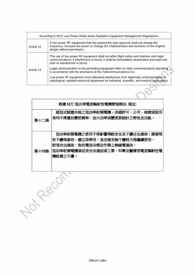
Silicon Labs
According to NCC Low Power Radio Wave Radiation Equipment Management Regulations:
Article 12
A low-power RF equipment that has passed the type approval shall not change the frequency, increase the power or change the characteristics and functions of the original design without permission.
Article 14
The use of low-power RF equipment shall not affect flight safety and interfere with legal communications; if interference is found, it shall be immediately deactivated and improved until no interference is found.
Legal communication in the preceding paragraph refers to radio communications operating in accordance with the provisions of the Telecommunications Act.
Low-power RF equipment must withstand interference from legitimate communications or radiological, radiated electrical equipment for industrial, scientific, and medical applications.

Silicon Labs
14 RoHS Statement with a List of Banned Materials
WT12 meets the requirements of Directive 2002/95/EC of the European Parliament and of the Council on the Restriction of Hazardous Substance (RoHS)
The following banned substances are not present in WT11, which is compliant with RoHS:
• Cadmium
• Lead
• Mercury
• Hexavalent chromium
• PBB (Polybrominated Bi-Phenyl)
• PBDE (Polybrominated Diphenyl Ether)

Silicon Laboratories Inc.400 West Cesar ChavezAustin, TX 78701USA
www.silabs.com
IoT Portfoliowww.silabs.com/IoT
SW/HWwww.silabs.com/simplicity
Qualitywww.silabs.com/quality
Support & Communitywww.silabs.com/community
Simplicity StudioOne-click access to MCU and wireless tools, documentation, software, source code libraries & more. Available for Windows, Mac and Linux!
DisclaimerSilicon Labs intends to provide customers with the latest, accurate, and in-depth documentation of all peripherals and modules available for system and software imple-menters using or intending to use the Silicon Labs products. Characterization data, available modules and peripherals, memory sizes and memory addresses refer to each specific device, and “Typical” parameters provided can and do vary in different applications. Application examples described herein are for illustrative purposes only. Silicon Labs reserves the right to make changes without further notice to the product information, specifications, and descriptions herein, and does not give warranties as to the accuracy or completeness of the included information. Without prior notification, Silicon Labs may update product firmware during the manufacturing process for security or reliability reasons. Such changes will not alter the specifications or the performance of the product. Silicon Labs shall have no liability for the consequences of use of the infor-mation supplied in this document. This document does not imply or expressly grant any license to design or fabricate any integrated circuits. The products are not designed or authorized to be used within any FDA Class III devices, applications for which FDA premarket approval is required or Life Support Systems without the specific written consent of Silicon Labs. A “Life Support System” is any product or system intended to support or sustain life and/or health, which, if it fails, can be reasonably expected to result in significant personal injury or death. Silicon Labs products are not designed or authorized for military applications. Silicon Labs products shall under no circumstances be used in weapons of mass destruction including (but not limited to) nuclear, biological or chemical weapons, or missiles capable of delivering such weapons. Silicon Labs disclaims all express and implied warranties and shall not be responsible or liable for any injuries or damages related to use of a Silicon Labs product in such unauthorized applications. Note: This content may contain offensive terminology that is now obsolete. Silicon Labs is replacing these terms with inclusive language wherever possible. For more information, visit www.silabs.com/about-us/inclusive-lexicon-project
Trademark InformationSilicon Laboratories Inc.®, Silicon Laboratories®, Silicon Labs®, SiLabs® and the Silicon Labs logo®, Bluegiga®, Bluegiga Logo®, Clockbuilder®, CMEMS®, DSPLL®, EFM®, EFM32®, EFR, Ember®, Energy Micro, Energy Micro logo and combinations thereof, “the world’s most energy friendly microcontrollers”, Ember®, EZLink®, EZRadio®, EZRadioPRO®, Gecko®, Gecko OS, Gecko OS Studio, ISOmodem®, Precision32®, ProSLIC®, Simplicity Studio®, SiPHY®, Telegesis, the Telegesis Logo®, USBXpress® , Zentri, the Zentri logo and Zentri DMS, Z-Wave®, and others are trademarks or registered trademarks of Silicon Labs. ARM, CORTEX, Cortex-M3 and THUMB are trademarks or registered trademarks of ARM Hold-ings. Keil is a registered trademark of ARM Limited. Wi-Fi is a registered trademark of the Wi-Fi Alliance. All other products or brand names mentioned herein are trademarks of their respective holders.