www.bzupages.com presentation on: electromagnetism topic: semiconductors presented to: sir.tariq...
TRANSCRIPT

www.bzupages.com
Presentation on: ELECTROMAGNETISM
Topic: SEMICONDUCTORS
Presented to: SIR.TARIQ BHATTI
Program: BsIT-3rd Department of Computer ScienceBZU , Multan

www.bzupages.com
Group Members
>MOHAMMAD IMRAN KHAN 07-37
>TAHA KHAN 07-06
>BEENISH JAHANGIR 07-04
>TAYYABA JAHANGIR 07-33

www.bzupages.com
MOHAMMAD IMRAN KHANRoll#07-37
>SEMICONDUCTOR
>SILICON CRYSTALS
>TYPES OF SEMICONDUCTOR
>INTRINSIC SEMICONDUCTOR
>EXTRINSIC SEMICONDUCTOR

www.bzupages.com
SemiconductorsMaterials that are
neither conductor nor insulator.
Element with 4 valance electrons is the best semiconductor.
They contains free electrons.
Element with electrical properties between those of conductors and insulators.

www.bzupages.com
Difference between semiconductor and conductor is because of the existence of holes, present in semiconductors.
For example; GermaniumSilicon

www.bzupages.com
Silicon crystalsAs an insulator:
Perfect insulator at 25°C8 valance electrons, covalently bonded with
the neighboring atoms.
As a conductor:act as conductor at ambient temperature
(above -273°C) An electron gains energy, creating a vacancy
in valence shell (hole), and move to bigger orbit. Hence, become a free electron.

www.bzupages.com
Recombination:Merging of free electron and a hole.
Lifetime:Amount of time for the creation and disappearance of free electron

www.bzupages.com
Intrinsic semiconductor
Pure semiconductors.Because of thermal
energy, equal numbers of electrons & holes are present.
These are often called as ‘carriers’ because they carry charge from one part to another.
These holes & electrons move in opposite direction.

www.bzupages.com
Extrinsic semiconductor
Doped semiconductor is called extrinsic semiconductor.
Doping:A way to increase
conductivity of semiconductor.Adding impurity atoms to
intrinsic crystal to alter its conductivity.

www.bzupages.com
Increasing free electrons:Adding pantavalent atoms, e.g; Arsenic,
Antimony, PhosphorusThey are also called donar impurities,as
they donate an extra electron.
Greater the impurity added, greater will be the conductivity.
Lightly-doped semi- conductors has high resistance.
Heavily-doped semi- conductors has low resistance.

www.bzupages.com
Increasing the holes:Adding trivalent impurity, e.g;
Aluminium, Boron,Gallium.Also called acceptor atom, because
hole can accept a free electron.

www.bzupages.com
TAHA KHANRoll#07-06
>N-TYPE SEMICONDUCTOR >P-TYPE SEMICONDUCTOR
>THE UNBIASED DIODE
>PN-JUNCTION
>DEPLETION LAYER

www.bzupages.com
DEFRENCE BETWEEN INTRINSIC AND EXTRINSIC SEMICONDUCTORS
www.bzupages.com
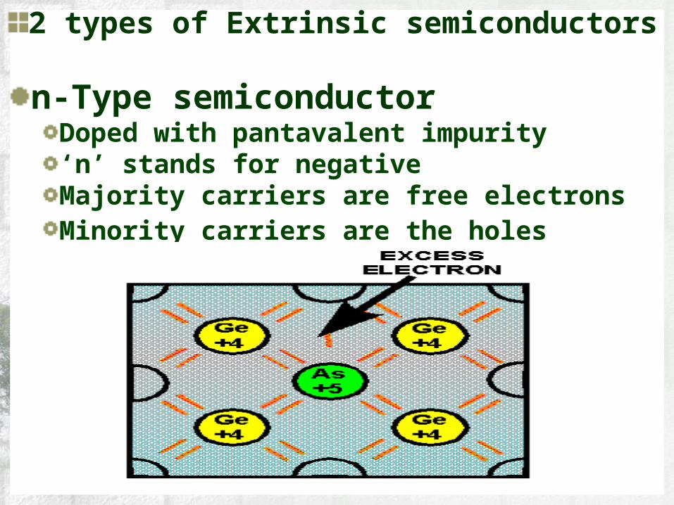
2 types of Extrinsic semiconductors
n-Type semiconductorDoped with pantavalent impurity‘n’ stands for negativeMajority carriers are free electronsMinority carriers are the holes

www.bzupages.com
p-Type semiconductorDoped with trivalent impurity ‘p’ stands for positiveMajority carriers are holesMinority carriers are free electrons

www.bzupages.com
Unbiased Diode
Diode explains, two electrodesIt is electrically neutralAlso called junction diode or pn-
crystal

www.bzupages.com
pn-junctionBorder between p-type & n-
type semiconductors.Lead to inventions like, diode,
transistors, & integrated circuits.

www.bzupages.com
The depletion layerFree electrons diffuses from n-type to p-
type, converting the pentavalent atom in ‘n’ into positive ion and trivlent in ‘p’ into negative ion
Each pair of negative and positive ions at the junction is called Dipole
This depreted region around the junction, having no charges but only ions, is called Depletion region

www.bzupages.com
BEENISH JAHANGIRRoll#07-04
>BARRIER POTENTIAL & TEMPRATURE
>FORWARD BIAS
>REVERSE BIAS
>CURRENT IN REVERSE BIAS

www.bzupages.com
Barrier Potential
Electric field between positive and negative ions
Act as a barrier and causes no diffusion of free electrons from ‘n’ to ‘p’
The electric field between ions is equivalent to difference of potential
At 25°C the Barrier potential for; Germanium Diode is 0.3V Silicon Diode is 0.7V

www.bzupages.com
BARRIER POTENTIAL &TEMPERATURE
Junction temperature >Temperature inside the diode
Ambient temperature >Temperature outside the diode
Conducting diode>when Junction temperature is greater then Ambient temperature
>Less barrier potential at higher temperature
A barrier potential of a silicon diode decreases by 2mV for each degree celsius rise.
V/T=-2mV/°C

www.bzupages.com
Forward biasDC source across dioden-type connected to negative terminal of the
batteryp-type connected to positive terminal of the
battery

www.bzupages.com
Conduction of current is in forward direction because of flow of free electron
No current if DC voltage is less then barrier potential
Continuous current if DC voltage is greater then barrier potential

www.bzupages.com
Reverse biasn-type connected to positive terminal of
the battery
p-type connected to negative terminal of the battery
negative terminal attracts the holes in ‘p’Positive terminal attracts the free
electrons in ‘n’

www.bzupages.com
Depletion layer gets wider (because of ions created around the junction )
Greater the reverse voltage greater will be the potential

www.bzupages.com
Current in reverse biased semiconductor
Saturation current >A very small current because of minority carriers and electron- hole pair inside the depletion layer because of thermal energy..
Surface- leakage current >Caused by surface impurity and imperfection in the crystal structure.
Approximately ZERO current.

www.bzupages.com
TAYYABA JAHANGIR Roll#07-33
>ENERGY LEVELS
>ENERGY BANDS
>ENERGY BAND IN INTRINSIC SEMICONDUCTOR
>N-TYPE ENERGY BAND
>P-TYPE ENERGY BAND

www.bzupages.com
ENERGY LEVELSHigher energy in larger
orbitElectron gain energy
when lifted to larger orbit
Which has more potential after lifting
This Energy is provided by heat ,light and voltage
Falling electron radiate light
Electron lose energy in form of heat ,light, radiation when falls to lower orbit

www.bzupages.com
ENERGY BANDSElectron of an isolated silcon atom are
bound to the neucleus having distinct energy level
In a solid, energy level of these isolated atom splits into sub-levels called discrete states
These states are so close that they appear as a continuous energy band

www.bzupages.com
FORBIDDEN GAPA range of energy states
between two consective permissible energy bands which cannot be occupied by electron
VALANCE BANDThe energy band in the
outer most shell of an atom occupying free electron
It is either completely or partially filled but never empty
Conduction is because of movement of holes

www.bzupages.com
CONDUCTION BANDAbove the valance bandElectron move freely May be empty or partially filled Conduction is because of movement of
free electronBands below valance band take no part in
conduction process because they are completely filled

www.bzupages.com
ENERGY BAND IN INTRINSIC SEMICONDUCTOR
Partially filled conduction & valance band
A narrow forbidden gap of order 1eV between conduction band & valance band
www.bzupages.com
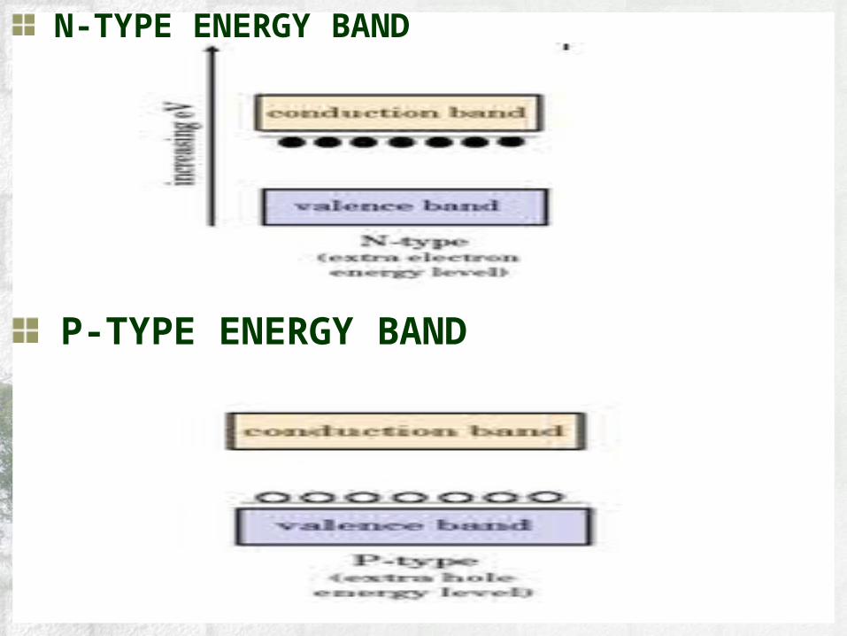
N-TYPE ENERGY BAND
P-TYPE ENERGY BAND

www.bzupages.com
COMPARISON