x-ray absorption spectroscopy - home - university of kent of electrons • current in wire is a flow...
TRANSCRIPT

Dr. Gavin Mountjoy, University of Kent, UK
Electron Microscopy
Nell'ambito del programma "Visiting Professor", finanziato dalla Regione Sardegna.
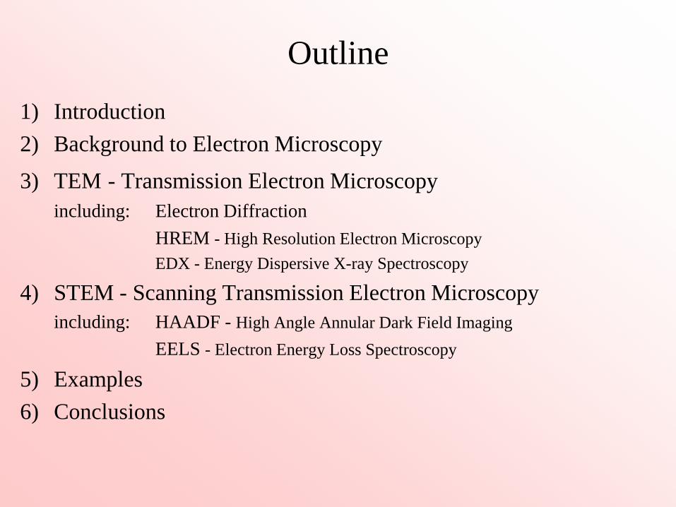
Outline1) Introduction 2) Background to Electron Microscopy3) TEM - Transmission Electron Microscopy
including: Electron DiffractionHREM - High Resolution Electron MicroscopyEDX - Energy Dispersive X-ray Spectroscopy
4) STEM - Scanning Transmission Electron Microscopyincluding: HAADF - High Angle Annular Dark Field Imaging
EELS - Electron Energy Loss Spectroscopy
5) Examples6) Conclusions
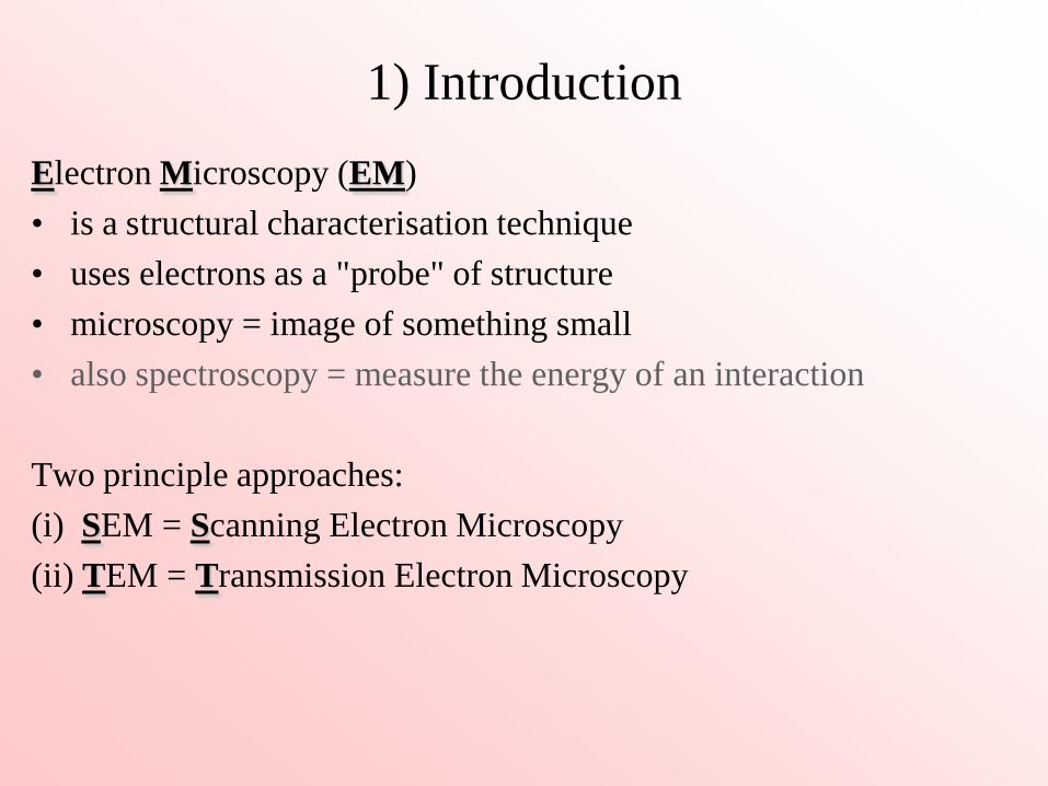
1) IntroductionElectron Microscopy (EM)• is a structural characterisation technique• uses electrons as a "probe" of structure• microscopy = image of something small• also spectroscopy = measure the energy of an interaction
Two principle approaches:(i) SEM = Scanning Electron Microscopy(ii) TEM = Transmission Electron Microscopy

Structural characterisation techniques• study the interaction of a "probe" with a sample• knowledge of interaction → information about structure• different types of probes → different types of interactions

• different types of probes– electromagnetic radiation– particles– physical contact
→ different energy– used for spectroscopy
different wavevector– used for scattering

Electrons• electrons are elementary particles
– charge (-1) or -1.6 10-19 Coulomb, mass 9.1 10-31 kg– most interactive and fastest moving of common particles
• E = kinetic energy in electron volts (eV) or kilo eV (keV)where 1 eV = 1.6 10-19 J, and valence electrons have E ~ eV
• wave-particle duality from Quantum Mechanics– electrons are waves with wavelength λ
• e.g. 200 keV electron has λ=0.027Å, – Note: velocity will be 20% of the speed of light!
(1) wave property of electrons means they can be used for imaging
( )( )keVE
A 39.0=λ
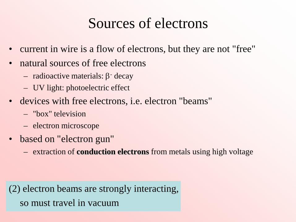
Sources of electrons• current in wire is a flow of electrons, but they are not "free"• natural sources of free electrons
– radioactive materials: β- decay– UV light: photoelectric effect
• devices with free electrons, i.e. electron "beams"– "box" television– electron microscope
• based on "electron gun"– extraction of conduction electrons from metals using high voltage
(2) electron beams are strongly interacting, so must travel in vacuum
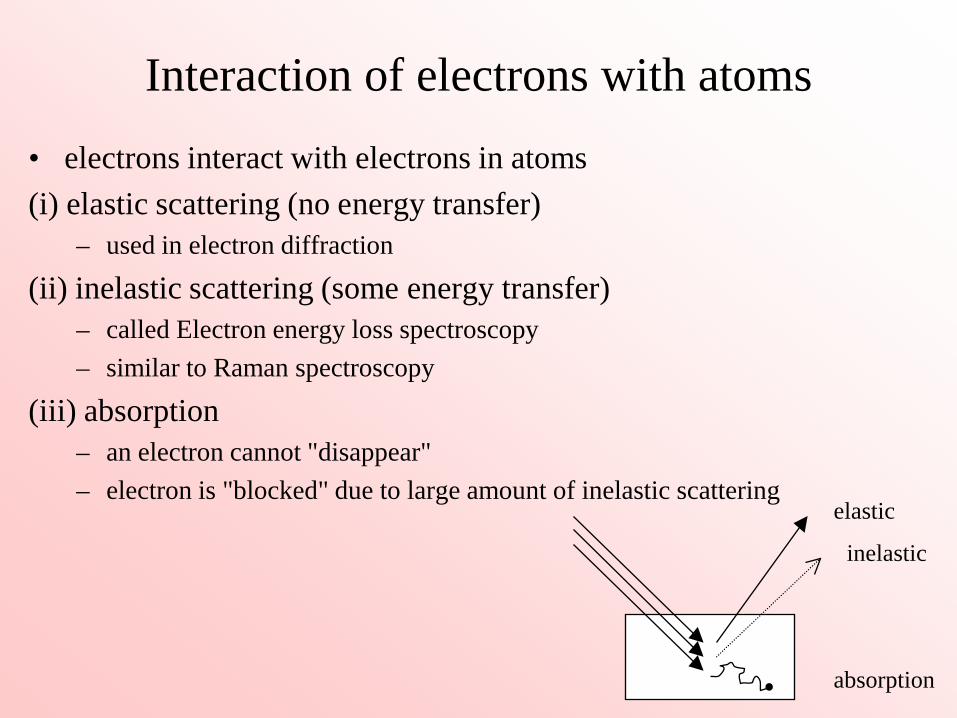
Interaction of electrons with atoms• electrons interact with electrons in atoms(i) elastic scattering (no energy transfer)
– used in electron diffraction
(ii) inelastic scattering (some energy transfer)– called Electron energy loss spectroscopy– similar to Raman spectroscopy
(iii) absorption– an electron cannot "disappear"– electron is "blocked" due to large amount of inelastic scattering
elastic
inelastic
absorption
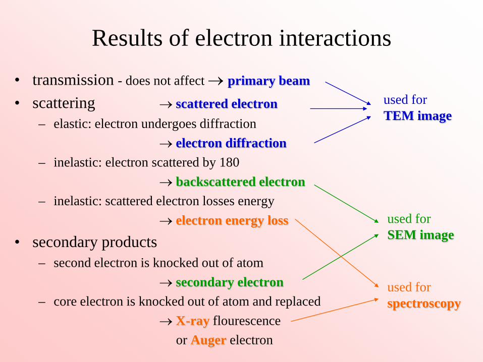
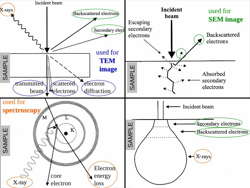
Results of electron interactions• transmission - does not affect → primary beam
• scattering → scattered electron– elastic: electron undergoes diffraction
→ electron diffraction– inelastic: electron scattered by 180
→ backscattered electron– inelastic: scattered electron losses energy
→ electron energy loss
• secondary products– second electron is knocked out of atom
→ secondary electron– core electron is knocked out of atom and replaced
→ X-ray flourescence or Auger electron
used for TEM image
used for spectroscopy
used for SEM image
electrondiffraction
used for SEM image
SA
MP
LE
SA
MP
LES
AM
PLE
core electron
Electronenergy loss
used for spectroscopy
SA
MP
LE
transmittedbeam
scatteredelectrons
used for TEM image
Object
ImageLens
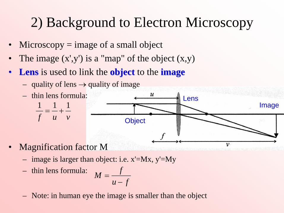
2) Background to Electron Microscopy• Microscopy = image of a small object• The image (x',y') is a "map" of the object (x,y)• Lens is used to link the object to the image
– quality of lens → quality of image– thin lens formula:
• Magnification factor M– image is larger than object: i.e. x'=Mx, y'=My– thin lens formula:
– Note: in human eye the image is smaller than the object
vuf111
+=
fufM−
=

Resolution of image• resolution ∆r = smallest detail of object in image
• resolution is limited due to size of lens– some of the light from the object is "lost"
• size of lens = semi-angle of aperture α
• Rayleigh formula:(refractive index n)
(3) electron wavelength λmuch smaller than light
αλ
sin61.0
nr =∆
∆r
Object
Lens
α
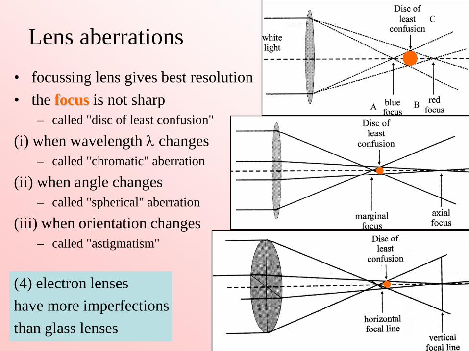
Lens aberrations• focussing lens gives best resolution • the focus is not sharp
– called "disc of least confusion"
(i) when wavelength λ changes– called "chromatic" aberration
(ii) when angle changes– called "spherical" aberration
(iii) when orientation changes– called "astigmatism"
(4) electron lenses have more imperfections than glass lenses
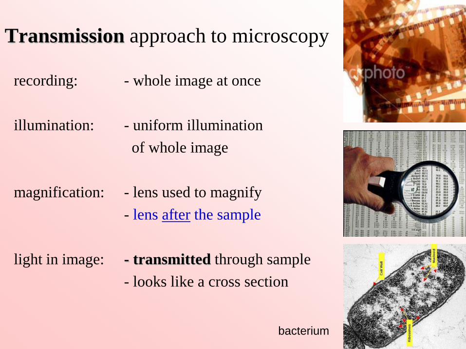
Transmission approach to microscopy
recording:
illumination:
magnification:
light in image:
- whole image at once
- uniform illumination of whole image
- lens used to magnify- lens after the sample
- transmitted through sample- looks like a cross section
bacterium
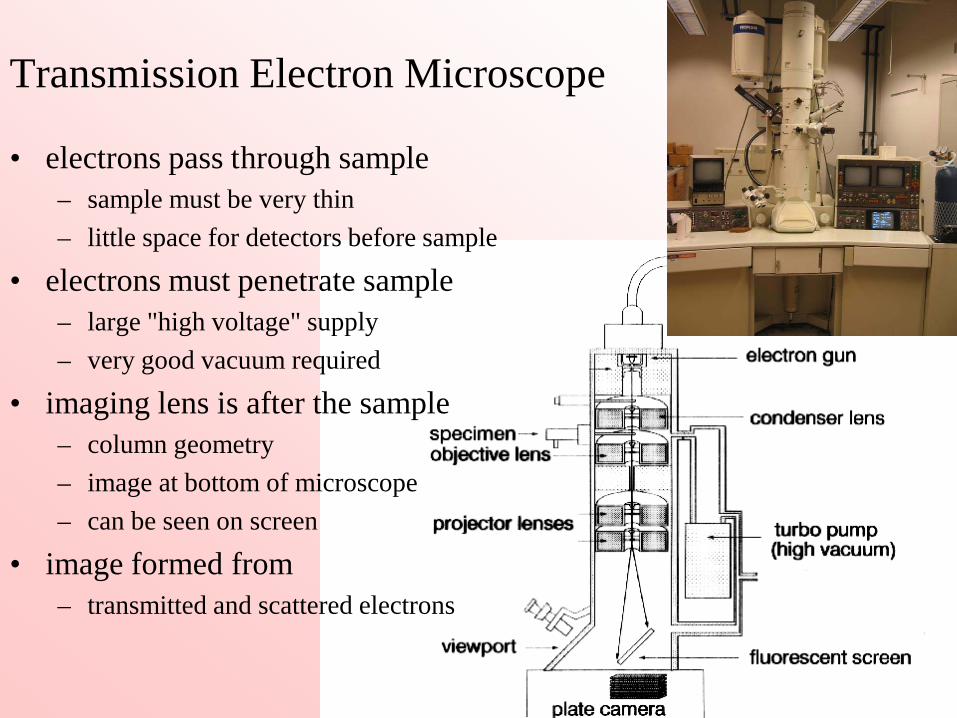
Transmission Electron Microscope
• electrons pass through sample– sample must be very thin– little space for detectors before sample
• electrons must penetrate sample– large "high voltage" supply– very good vacuum required
• imaging lens is after the sample– column geometry– image at bottom of microscope – can be seen on screen
• image formed from– transmitted and scattered electrons
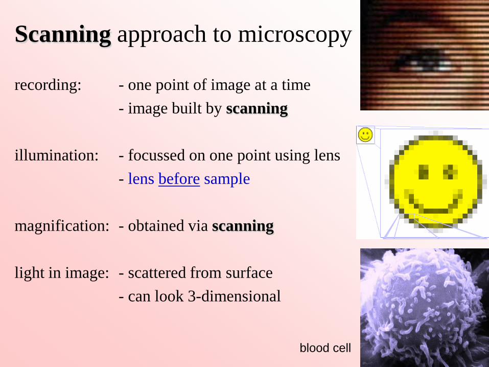
Scanning approach to microscopy
recording:
illumination:
magnification:
light in image:
- one point of image at a time- image built by scanning
- focussed on one point using lens- lens before sample
- obtained via scanning
- scattered from surface- can look 3-dimensional
blood cell
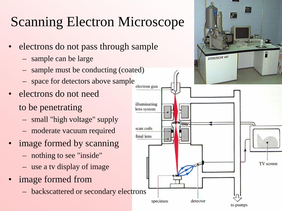
Scanning Electron Microscope
• electrons do not pass through sample– sample can be large– sample must be conducting (coated)– space for detectors above sample
• electrons do not need to be penetrating– small "high voltage" supply– moderate vacuum required
• image formed by scanning– nothing to see "inside"– use a tv display of image
• image formed from– backscattered or secondary electrons
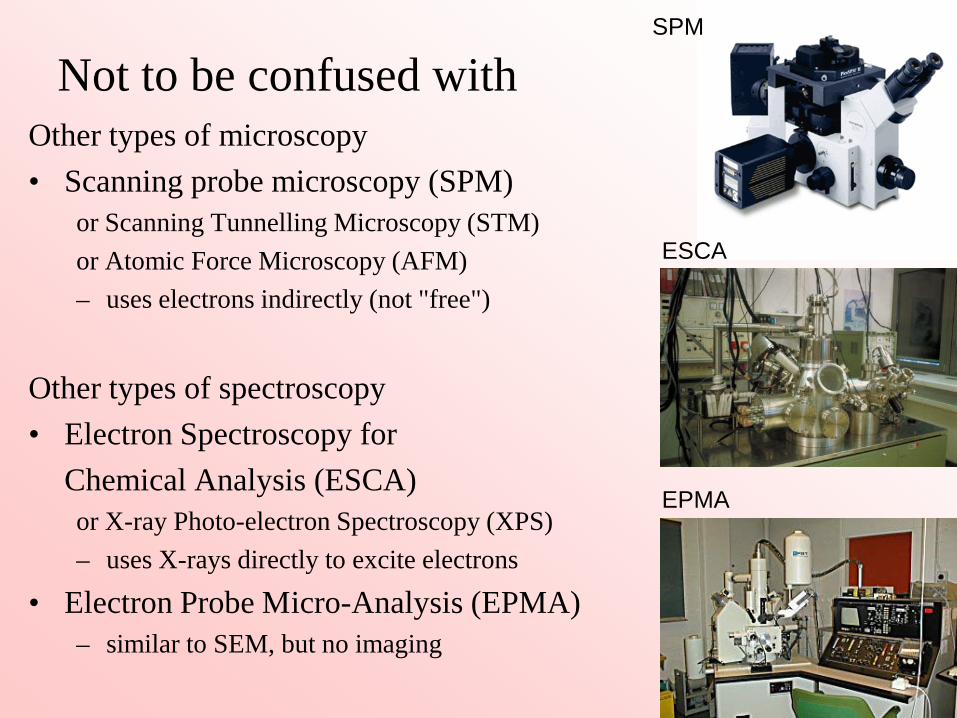
Not to be confused withOther types of microscopy• Scanning probe microscopy (SPM)
or Scanning Tunnelling Microscopy (STM)or Atomic Force Microscopy (AFM)– uses electrons indirectly (not "free")
Other types of spectroscopy• Electron Spectroscopy for
Chemical Analysis (ESCA)or X-ray Photo-electron Spectroscopy (XPS)– uses X-rays directly to excite electrons
• Electron Probe Micro-Analysis (EPMA)– similar to SEM, but no imaging
SPM
ESCA
EPMA

3) TEM: EquipmentSource of electrons• thermionic emission (electron gun)
– heating wire helps electrons to escape– made from tungsten (W) or LaB6
– moderate brightness
• field emission gun (FEG)– very sharp metal point helps electrons to escape– high brightness, but requires ultra high vacuum
thermionic emission (LaB6) field emission
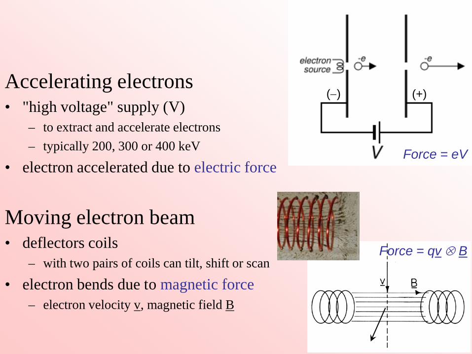
Accelerating electrons• "high voltage" supply (V)
– to extract and accelerate electrons– typically 200, 300 or 400 keV
• electron accelerated due to electric force
Moving electron beam• deflectors coils
– with two pairs of coils can tilt, shift or scan
• electron bends due to magnetic force– electron velocity v, magnetic field B
Force = eV
Force = qv ⊗ B
(+)(−)

Electron lens
• Lens is used to link the object to the image– (1) light spreads out from object– (2) lens causes light to bend more at high angles– (3) image formed when light converges on image
• optical lens (for light) is made of glass– light bends due to refractive index of glass
• electron lens is made of magnetic field• electron bends due to magnetic force
– non-uniform magnetic field B causeselectron velovity v to bend more at high angles
• resolution ∆r varies from ~3 Å to 1.7 Å
(1) Object
(3) Image(2) Lens
Force = qv ⊗ B
v
B
(1) Object
(2) Lens
(3) Image

Recording image
Detecting electrons• fluorescent screen (at bottom of microscope)
– like the front of a "box" tv screen (CRT)– operator looks with their eyes!
• photographic camera– uses special photographic negatives– exposure time of ~1 sec
• CCD camera (like a digital camera)– semiconductor device– can be directly linked to a computer
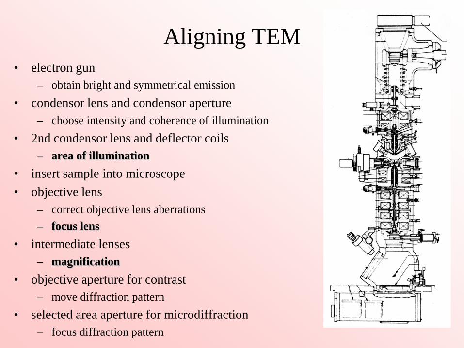
Aligning TEM• electron gun
– obtain bright and symmetrical emission• condensor lens and condensor aperture
– choose intensity and coherence of illumination• 2nd condensor lens and deflector coils
– area of illumination• insert sample into microscope• objective lens
– correct objective lens aberrations– focus lens
• intermediate lenses– magnification
• objective aperture for contrast– move diffraction pattern
• selected area aperture for microdiffraction– focus diffraction pattern

TEM: sample preparation• sample must be thin very thin
– TEM: thickness < 1 µm– HREM: thickness < 50 nm– biological samples must be frozen
• sample is supported on copper microscope grid• sample preparation
(1) grinding to make a powder(2) standard thinning: composite, diamond saw, grinder, dimpler, ion-beam (3) "focussed ion beam" (FIB) to cut the sample
• sample may become damaged– due to "high voltage" electron beam

TEM: image contrast
• transmission of electronsIT = I0exp(-µt)– thickness contrast (t)– mass contrast (µ depends on atomic no. Z)
• scattering contrast– scattering deviates electrons
• objective aperture is used to block electrons– is located in the "focal plane"– bright field: only un-scattered electrons– dark field: only scattered electrons
• stronger effect for crystalline regions– diffraction deviates electrons more
objectivelens
objectiveaperture
sample
focal plane

CaCO3 aragonite
bright field
nanostructured Nb filmsthickness contrast
dark field
scattering contrast
objective lens
objective aperture
sample
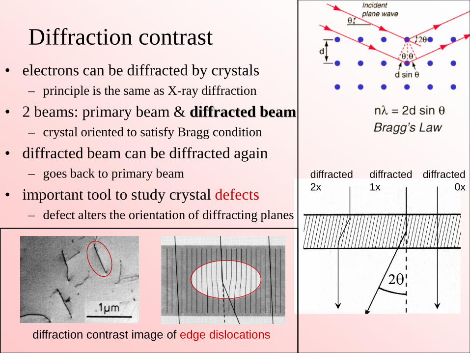
Diffraction contrast• electrons can be diffracted by crystals
– principle is the same as X-ray diffraction
• 2 beams: primary beam & diffracted beam– crystal oriented to satisfy Bragg condition
• diffracted beam can be diffracted again– goes back to primary beam
• important tool to study crystal defects– defect alters the orientation of diffracting planes
diffracted0x
diffracted2x
diffracted1x
diffraction contrast image of edge dislocations

Electron diffraction– in X-ray diffraction the angle is measured directly– in electron diffraction the angle is ~0.5 degree
• objective lens bends the electrons to make a diffraction pattern• intermediate lens magnifies the diffraction pattern
– this is "diffraction mode"
• selected area aperture is used to choose region of sample– is called "microdiffraction"– e.g. 10-15 gram of sample
sample
objective lens
intermediatelens
intermediatelens
diffraction pattern
imageimage
selected area aperture
image mode diffraction mode
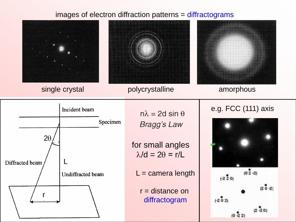
images of electron diffraction patterns = diffractograms
single crystal polycrystalline amorphous
for small anglesλ/d = 2θ = r/L
L = camera length
r = distance on diffractogram
L
r
2θ
e.g. FCC (111) axis

High resolution electron microscopy• scattering contrast has low resolution
– because objective aperture limits size of objective lens
• highest resolution requires no objective aperture– both undiffracted and diffracted beams form image
• sample is oriented along crystal axis– electrons travel through crystal in Block waves– (or) electrons are diffracted by parallel planes– diffracted electrons have different phase
• phase contrast occurs due to phase difference between waves– e.g. destructive interference
makes image darker
lens gives π/2 phase shift in diffracted beamsw.r.t. main beam

HREM images of crystals• image shows planes or columns of atoms
– sample must be very thin so that diffracted electron remains in column
• objective lens alters the phase of diffracted electrons– determined by "contrast transfer function" (CTF) of the lens– best resolution obtained for "Scherzer" focus– image appearance varies strongly with focus
HREM image
effect oflens focuson image of GaAs [110]
planes of atoms columns of atoms
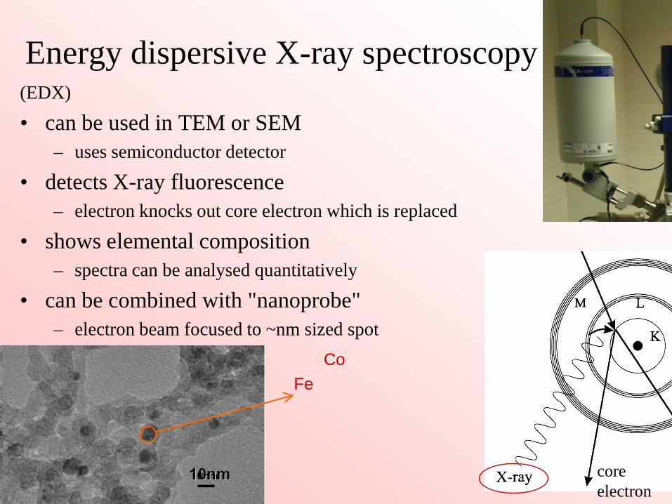
Energy dispersive X-ray spectroscopy(EDX)
• can be used in TEM or SEM – uses semiconductor detector
• detects X-ray fluorescence– electron knocks out core electron which is replaced
• shows elemental composition– spectra can be analysed quantitatively
• can be combined with "nanoprobe"– electron beam focused to ~nm sized spot
core electron
FeCo
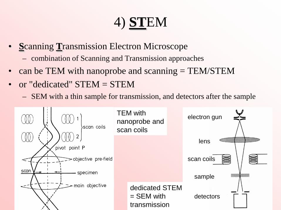
4) STEM• Scanning Transmission Electron Microscope
– combination of Scanning and Transmission approaches
• can be TEM with nanoprobe and scanning = TEM/STEM• or "dedicated" STEM = STEM
– SEM with a thin sample for transmission, and detectors after the sample
TEM withnanoprobe andscan coils
dedicated STEM = SEM withtransmission
electron gun
scan coils
sample
detectors
lens
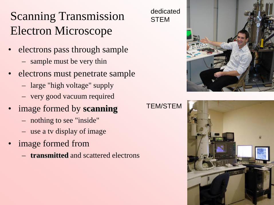
Scanning Transmission Electron Microscope• electrons pass through sample
– sample must be very thin
• electrons must penetrate sample– large "high voltage" supply– very good vacuum required
• image formed by scanning– nothing to see "inside"– use a tv display of image
• image formed from– transmitted and scattered electrons
dedicated STEM
TEM/STEM
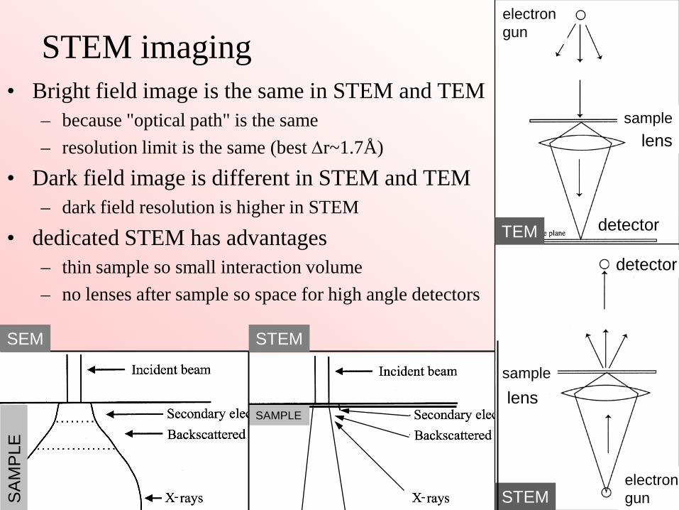
STEM imaging• Bright field image is the same in STEM and TEM
– because "optical path" is the same– resolution limit is the same (best ∆r~1.7Å)
• Dark field image is different in STEM and TEM– dark field resolution is higher in STEM
• dedicated STEM has advantages– thin sample so small interaction volume– no lenses after sample so space for high angle detectors
samplelens
electron gun
detector
STEM
TEM
detector
sample
lens
electron gunS
AM
PLE
SAMPLE
SEM STEM
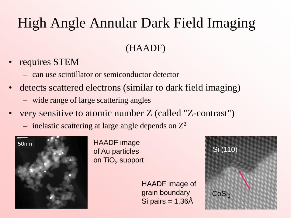
High Angle Annular Dark Field Imaging(HAADF)
• requires STEM– can use scintillator or semiconductor detector
• detects scattered electrons (similar to dark field imaging)– wide range of large scattering angles
• very sensitive to atomic number Z (called "Z-contrast")– inelastic scattering at large angle depends on Z2
HAADF imageof Au particleson TiO2 support
50nm
CoSi2
Si (110)
HAADF image of grain boundarySi pairs = 1.36Å
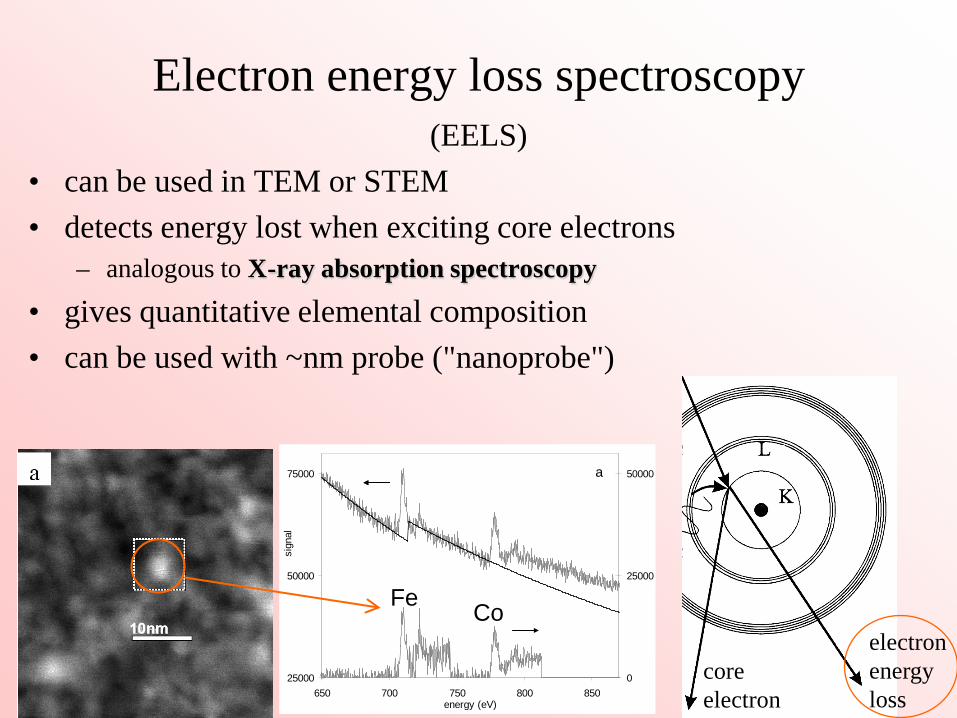
Electron energy loss spectroscopy(EELS)
• can be used in TEM or STEM • detects energy lost when exciting core electrons
– analogous to X-ray absorption spectroscopy
• gives quantitative elemental composition • can be used with ~nm probe ("nanoprobe")
25000
50000
75000
650 700 750 800 850energy (eV)
sign
al
0
25000
50000a
Fe Co
core electron
electronenergy loss

Force = qv ⊗ B
EELS spectrometer• transmitted electrons have energy E'<E
– E = energy of electron gun, e.g. 200 keV
• EELS spectrometer measures energy E'– energy loss is ∆E = E−E'
• spectrometer uses a uniform magnetic field– electrons are deviated due to magnetic force– radius of circular path depends on velocity and E'– same principles as mass spectrometer
• electron detector– serial (diode): measure single point on spectrum– parallel (semiconductor): measure whole spectrum faster e-
smaller ∆Eslower e-
larger ∆E

EELS spectra• zero loss peak
– unscattered electrons with ∆E=0
• low-loss region– ∆E up to 30eV – due to excitation of "plasmons"
• high-loss region (or "core" loss)– ∆E up to 2 keV – due to excitation of core electrons
• edges in EELS spectra– K-edges of light elements (Z<15)– L-edges of transition metals– same as X-ray absorption edges
Energy loss (eV)
Energy loss (eV)
B K-edge
N K-edge
zero loss peak (elastic)
plasmon loss
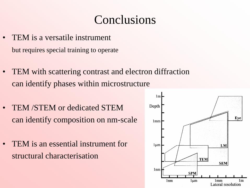
Conclusions• TEM is a versatile instrument
but requires special training to operate
• TEM with scattering contrast and electron diffraction can identify phases within microstructure
• TEM /STEM or dedicated STEM can identify composition on nm-scale
• TEM is an essential instrument for structural characterisation

Acknowledgements• Collaborators:
– A. Falqui, A. Corrias, MF. Casula, D. Loche, M. Gass, W. Parak
• Microscopy facilities:– E. Snoeck (CEMES), (TEMSCAN), A. Bleloch (SuperSTEM)
• Funding organisations:– Marie Curie Fellowship (EU), ESTEEM Programme (EU), EPSRC (UK)