x-ray detectors for the dynamic compression sector · detector; the number of -rays/pixel/frame is...
TRANSCRIPT

X-ray Detectors for the
DYNAMIC COMPRESSION SECTOR
AT THE ADVANCED PHOTON SOURCE

The Dynamic Compression Sector (DCS) at the Advanced Photon Source (APS), a DOE/NNSA sponsored user facility, constitutes a new paradigm for understanding the dynamic compression response of materials at multiple length scales. A key scientific feature of dynamic compression experiments coupled to high-energy, tunable X-ray probes is their ability to afford time-resolved, in-situ, atomistic-scale investigations of condensed matter phenomena “on-the-fly” or as they occur in single event experiments. The DCS capabilities address long-standing scientific challenges with the potential for unprecedented scientific payoff in the areas of structural changes, deformation and fracture, and chemical reactions. In addition, the DCS provides hands-on training for the next generation of scientists in this exciting field.
Washington State University leads the effort to develop and build the DCS experimental infrastructure and capabilities in collaboration with the APS; DOE/NNSA National Laboratories (Los Alamos, Lawrence Livermore, and Sandia); Department of Defense Laboratories, including the Army Research Laboratory and Naval Research Laboratory; and academic institutions.
[email protected] ∙ 9700 S. Cass Ave. (Building 438F), Lemont, IL 60439 ∙ dcs-aps.wsu.edu

X-ray Detectors for the Dynamic Compression Sector at the Advanced Photon Source
Stefan J. Turneaure, Steve Wang, Timothy Graber, Kurt Zimmerman, and Yogendra M. Gupta
Institute for Shock Physics Washington State University
April 2015
i

PREFACE
This report describes work carried out by the Institute for Shock Physics, Washington State University to describe representative configurations for X-ray diffraction and imaging experiments to be performed at the Dynamic Compression Sector (DCS). The material in this report is based upon work supported by the Department of Energy/National Nuclear Security Administration, under Award Number DE-NA0002442. This report was prepared as an account of work sponsored by an agency of the United States Government. Neither Washington State University, the United States Government nor any agency thereof, nor any of their employees, makes any warranty, express or implied, or assumes any legal liability or responsibility for the accuracy, completeness, or usefulness of any information, apparatus, product, or process disclosed, or represents that its use would not infringe privately owned rights. Reference herein to any specific commercial product, process, or service by trade name, trademark, manufacturer, or otherwise does not necessarily constitute or imply its endorsement, recommendation, or favoring by Washington State University, the United States Government or any agency thereof. The views and opinions of authors expressed herein do not necessarily state or reflect those of the United States Government or any agency thereof.
ii
Abstract The Dynamic Compression Sector (DCS), located at the Advanced Photon Source (APS), has been established to examine dynamically compressed condensed matter in real-time with experimental durations varying from a few nanoseconds to microseconds. Advanced X-ray detectors, including ones not available today, are needed to fully realize the scientific potential of the DCS. We anticipate that several different detectors, optimized for different characteristics including spatial resolution, time resolution, and efficiency, would be used. For example, a common type of experiment at the DCS will involve X-ray diffraction measurements under plate impact loading and will require detectors with single X-ray photon sensitivity and near 100% quantum efficiency for 8-35 keV X-ray energies, 2048×2048 pixels with about 100×100 µm2 pixel size, dynamic range of 104 X-rays per pixel, frame rates up to 100 MHz, and on chip storage for 100 frames. Simultaneous imaging measurements are also desired, requiring detectors with sub-micron resolution and similar efficiency, frame rate, and dynamic range. This document describes representative configurations for X-ray diffraction and imaging experiments to be performed at the DCS. We also present simulation results for representative experiments to provide the number of X-rays expected to arrive at each pixel of an area detector during each ~100 ps duration X-ray pulse. Based in part on these simulations, the desired detector specifications for key measurements are provided. Currently available detector solutions are reviewed and areas for potential improvement are highlighted. We hope this report will stimulate interest in the detector community to develop solutions for the next 2-10 year time horizon.
iii

Table of Contents
I. Introduction ......................................................................................................................... 1
II. Drivers and Experimental Configurations .......................................................................... 2
III. Representative Simulations ................................................................................................. 4
IV. Detector Needs .................................................................................................................... 7
V. Existing and Potential Detector Options for Single Event Experiments ............................ 9
VI. Existing and Potential Detector Options for Longer Duration Single Event Experiments and Pump-probe Type Experiments .................................................................................. 14
VII. Summary and Path Forward.............................................................................................. 15
VIII. References ......................................................................................................................... 16
iv

I. Introduction
The Dynamic Compression Sector (DCS) at the Advanced Photon Source (APS), a first-of-a-kind experimental capability, links a high-energy, tunable X-ray beamline to state-of-the-art dynamic compression platforms. This novel development permits real-time X-ray measurements (diffraction, imaging, scattering) in dynamically compressed materials (peak stresses to over 350 GPa, and time-durations ranging from ~5ns to microsecond). Three of the four experimental stations (or hutches) have been developed for shock compression experiments using plate impact or laser drive loading. The fourth experimental station has been developed as a special-purpose station for a variety of dynamic experiments (utilizing mobile platforms) such as detonation chambers and Kolsky or split-Hopkinson bar loading. The durations of the DCS dynamic experiments can vary widely from several nanoseconds (laser-shock experiments) to a microsecond (plate impact experiments) to hundreds of microseconds (Kolsky bar experiments). The pulsed X-ray time structure of the APS is well suited for probing condensed matter dynamics during dynamic experiments. The APS storage ring lattice consists of 1296 equally spaced “buckets” (2.84 ns between buckets) each of which may either be filled or unfilled. The overall period of the 1,104 m circumference storage ring is 3.68 µs. Three specific bunch modes are most commonly operated: 24 bunch mode with 153.4 ns between equally spaced bunches, 324 bunch mode with 11.4 ns between equally spaced bunches, and a hybrid mode consisting of a superbunch separated from all other equally filled bunches by 1.59 µs. In principle, other bunch modes are possible, provided that the storage ring lattice remains stable. Recent specifications for the proposed APS upgrade to a Multi-Bend Achromat lattice are 48-324 equally spaced bunches corresponding to 11.4-77 ns between periodic bunches. Time resolved data in sub-microsecond duration shock compression experiments and/or longer duration dynamic experiments can be obtained by capturing X-ray images from the individual X-ray pulses of ~100 ps duration that arrive periodically at the detector. Optimal use of the pulsed X-rays at the APS for time-resolved measurements will require advanced detectors capable of capturing and storing images at the same time scale as the synchrotron time structures. The detector requirements will depend on the specific measurement type, such as diffraction or imaging, and the dynamic loading method, such as plate impact, laser drive, or Hopkinson bar. Common detector requirements for all experiments are that the detectors be two-dimensional integrating pixelated area detectors. In particular, large-format integrating two-dimensional pixelated detectors are required to capture the maximum information in each ~100 ps duration X-ray pulse. Several specific experimental configurations and representative simulations are presented in sections II and III, respectively. We have included simulations to provide the expected number of X-rays/pixel/bunch arriving at the detector; the number of X-rays/pixel/frame is a key parameter in detector choice and design. Desired detector parameters are provided in section IV. A review of existing and potential detectors is presented in section V for short duration (several microseconds or shorter) single event experiments. A review of existing and potential detectors for longer duration single event and/or repetitive pump-probe experiments is provided in section VI.
1

II. Drivers and Experimental Configurations
The DCS developments include two types of shock compression drivers: high velocity launchers for plate impact and a 100 J laser for direct drive laser shock experiments. A compact pulsed power machine for ramp compression experiments may be added in the future. Because of the different shock loading durations (~1 microsecond for plate impact and 5-10 nanoseconds for laser drive), detector needs for plate impact and laser drivers will be different. II.A Plate Impact Loading Figure 1 shows five potential configurations for plate impact experiments. The configurations shown in figures 1(a)-1(c) are for reflection geometry diffraction experiments which have a low divergence incident beam focused on the sample. The diffraction measurements in figures 1a and 1b are made at the sample side opposite to the sample impact side. The diffraction measurement in figure 1c is made at the sample impact surface. Figure 1d shows a transmission diffraction geometry in which the incident X-rays pass through the projectile, sample and X-ray window. For all of the diffraction configurations, the incident and diffracted beams pass through an X-ray window of low-Z material such as vitreous carbon, boron carbide, diamond, LiF, PMMA or Lexan. Figure 1(e) shows the geometry for imaging measurements using phase contrast imaging. These images are acquired with either a direct white beam with size of about 3 mm (H) × 2 mm (V) or a quasi-monochromatic pink beam focused by a KB mirror with an adjustable field of view. The beam passes through the sample perpendicular to the loading direction. Because the typical durations of plate impact experiments are about a microsecond, the timing of the data acquisition system is critical. Typical jitter of the impact time relative to the initiation of the projectile launch is about 1 ms or larger. Hence, it’s not possible to use the launch event to correlate the arrival of the X-ray bunches at the sample. Instead, the detector acquisition sequence will be triggered using a target mounted trigger signal such as piezoelectric pins or an
Figure 1: Configurations for plate impact experiments. (a) - (d) are for diffraction or scattering experiments and (e) is for imaging. The elements behind the orange arrows are mounted on the projectile.
2

optical trigger (Gupta et al., 1999). For a framing detector capable of recording multiple frames, recording will begin shortly before impact and stop some time after edge waves reach the probed volume. For a gated detector capable of capturing a single frame, an ambient image will be recorded before initiating the projectile launch and a single image will be recorded in the shocked state. II.B Laser Drive II.B.1 Single Event Laser Drive Because the typical loading duration for laser drives is about 5 to 10 ns, most laser drive experiments are expected to record a single image from a single X-ray bunch. Mechanical chopper systems will be used to pick out either the superbunch in the hybrid mode or one of the 24 equivalent bunches in the 24-bunch mode (Graber et al., 2011). The laser driver pulses have sufficiently low jitter to be correlated to the arrival of the desired X-ray pulse. For these experiments, the detector requirements are not as stringent as for the plate impact experiments. Fast gating or framing is not necessary because a chopper system can isolate a single X-ray pulse. Figure 2 shows a possible configuration for X-ray diffraction measurements in direct drive laser shock compression experiments. A thin sample is sandwiched between two X-ray windows and the beam passes through the sample along the loading direction. The area detector is perpendicular to the loading direction. For this configuration, the direct beam will be blocked. II.B.2 Pump-probe Laser Drive Laser drives are also well suited for time-resolved repetitive pump-probe type experiments. A Jülich beam chopper system can downshift the frequency of the X-ray bunches arriving at the sample to sub-kHz rates (Graber et al., 2011) and a moderately fast (sub-kHz frame rate) framing area detector can be used to obtain multiple images.
Figure 2: A configuration for X-ray diffraction measurements in direct drive laser shock experiments.
3
III. Representative Simulations
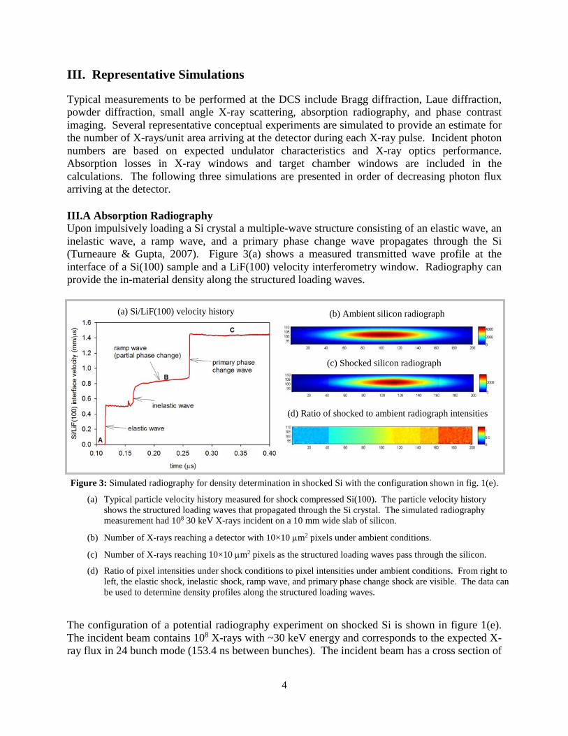
Typical measurements to be performed at the DCS include Bragg diffraction, Laue diffraction, powder diffraction, small angle X-ray scattering, absorption radiography, and phase contrast imaging. Several representative conceptual experiments are simulated to provide an estimate for the number of X-rays/unit area arriving at the detector during each X-ray pulse. Incident photon numbers are based on expected undulator characteristics and X-ray optics performance. Absorption losses in X-ray windows and target chamber windows are included in the calculations. The following three simulations are presented in order of decreasing photon flux arriving at the detector. III.A Absorption Radiography Upon impulsively loading a Si crystal a multiple-wave structure consisting of an elastic wave, an inelastic wave, a ramp wave, and a primary phase change wave propagates through the Si (Turneaure & Gupta, 2007). Figure 3(a) shows a measured transmitted wave profile at the interface of a Si(100) sample and a LiF(100) velocity interferometry window. Radiography can provide the in-material density along the structured loading waves.
The configuration of a potential radiography experiment on shocked Si is shown in figure 1(e). The incident beam contains 108 X-rays with ~30 keV energy and corresponds to the expected X-ray flux in 24 bunch mode (153.4 ns between bunches). The incident beam has a cross section of
Figure 3: Simulated radiography for density determination in shocked Si with the configuration shown in fig. 1(e).
(a) Typical particle velocity history measured for shock compressed Si(100). The particle velocity history shows the structured loading waves that propagated through the Si crystal. The simulated radiography measurement had 108 30 keV X-rays incident on a 10 mm wide slab of silicon.
(b) Number of X-rays reaching a detector with 10×10 µm2 pixels under ambient conditions.
(c) Number of X-rays reaching 10×10 µm2 pixels as the structured loading waves pass through the silicon.
(d) Ratio of pixel intensities under shock conditions to pixel intensities under ambient conditions. From right to left, the elastic shock, inelastic shock, ramp wave, and primary phase change shock are visible. The data can be used to determine density profiles along the structured loading waves.
(a) Si/LiF(100) velocity history (b) Ambient silicon radiograph
(c) Shocked silicon radiograph
(d) Ratio of shocked to ambient radiograph intensities
4

2000×200 µm2 and passes through a silicon slab 10 mm in width perpendicular to the shock compression direction. Figure 3(b) shows the number of X-rays/pixel arriving at a detector with 10×10 µm2 pixels for the ambient Si. Figure 3(c) shows the number of X-rays/pixel arriving at the detector while the structured longitudinal loading waves are in the 2 mm wide incident beam. Figure 3(d) shows the ratio of the X-rays/pixel in the shocked and ambient states. The elastic wave, inelastic wave, ramp wave, and primary phase change wave are visible from right to left in figure 3(d). III.B Laue Diffraction Figure 4 shows simulated Laue diffraction patterns for (a) an ambient α phase Fe(100) single crystal, for (b) mixed phase α Fe and ε Fe, and (c) for ε Fe in the peak state. The geometry of the simulated experiment is shown in figure 1(a). The incident beam is in the horizontal plane and has a 10-degree angle relative to the sample plane. The number of incident X-rays is 5×10⁵/0.1% BW from 8-30 keV, which is the expected X-ray flux for the 324 bunch mode (11.4 ns between bunches). The detector is located 4 cm from the sample and has 100×100 µm2 pixels.
III.C Powder Diffraction Figure 5 shows simulated diffraction patterns from single X-ray bunches for the 24 bunch mode for polycrystalline silicon under ambient conditions in figure 5(a), in a shocked mixed phase region in figure 5(b), and in the peak shocked state in figure 5(c). The geometry of the simulated shock experiment is shown in figure 1(a). The incident beam is in the horizontal plane and has a 15 degree angle relative to the sample plane. The incident beam has 2×10⁹ 12 keV X-rays with 2% bandwidth in each X-ray pulse. The detector is located 4 cm from the sample and has 100 x 100 µm2 pixels.
Figure 4: Simulated Laue diffraction patterns from Fe using configuration shown in figure 1a. (a) shows ambient Fe(100); (b) shows a mixture of α and ε phases; (c) shows the high pressure ε phase. The simulations correspond to single pulse measurements in 324 bunch mode with 5x10⁵ X-rays/0.1% BW from 8-30 keV. X-ray absorption in two 1 mm thick Lexan target chamber windows and a 2 mm thick B4C X-ray window is included. The detector is 4 cm from the sample center and has 100 x 100 µm2 pixels.
5

Figure 5: Simulated diffraction from polycrystalline Si. (a) is for ambient Si corresponding to A in figure 3a; (b) is for a mixture of ambient and high pressure phases corresponding to B in figure 3a; (c) is for the high pressure simple hexagonal phase corresponding to C in figure 3a. The simulations correspond to single pulse measurements for the 24 bunch mode with 2x10⁹ X-rays/frame with 12 keV energy and 2% bandwidth. X-ray absorption in two 1 mm thick Lexan target chamber windows and a 2 mm thick B4C X-ray window is included. The detector is 4 cm from the sample center and has 100 x 100 µm2 pixels.
6

Pixel size 100×100 µm2 Number of pixels 2000×2000 or greater Sensitivity Single photon Dynamic range 104 X-rays/pulse Frame rate Adjustable
> 6 MHz for 24-bunch > 100 MHz for 324 bunch
Number of frames 100 or greater Quantum Efficiency Near 100% (8-35 keV) Linearity Better than 1% Table I: Desired Detector Properties for Single Event Diffraction Experiments
IV. Detector Needs
IV.A Detectors for Recording Diffraction Data in Plate Impact Experiments Table I lists desired detector properties for time-resolved, diffraction measurements in plate impact experiments. An ideal detector would be able to frame at 100 MHz to record consecutive images for each X-ray pulse in the 324 bunch mode. An ideal detector would be able to provide continuous recording for a µs, which corresponds to about 100 frames in 324 bunch mode. The detector would ideally be able to record between 1-104 X-rays/pixel/bunch with good linearity. The small number of calculated X-rays/pixel/bunch in the powder diffraction simulations in the previous section highlights the importance of single X-ray sensitivity. Quantum efficiency should approach 100% in the full 8-35 keV energy range. For small area detectors, there is a tradeoff between detector angular resolution and angular range accepted by the detector. Angular resolution is increased by increasing the sample-to-detector distance at the expense of decreased total angular range coverage. A detector with 100×100 µm2 pixel size and 2000×2000 pixels or greater would likely cover sufficient angular area with sufficient resolution for most experiments. IV.B Detectors for Recording Imaging Data in Plate Impact Experiments An ideal detector for imaging is significantly different from an ideal detector for diffraction experiments, primarily in the requirements of larger dynamic range because of the higher X-ray fluxes incident on the detector and lower image contrast; better spatial resolution, ideally about 1 µm or better; and the ability to operate at a higher energy range of up to 100 keV with high quantum efficiency for imaging high Z materials. It will also be beneficial to image non-plate impact events for up to 5 µs duration which corresponds to roughly 500 frames in 324 bunch mode. Table II lists desired properties of a detector for plate impact radiography experiments.
IV.C Detectors for Single Event Laser Drive The detector properties listed in Tables I and II for plate impact experiments also apply to single event laser drive experiments with the exception that framing or rapid gating is not necessary. Because a single X-ray pulse may be isolated using choppers and shutters, many existing detectors may be used. For example, an ungated MAR165 CCD (phosphor/fiber taper/CCD
Effective pixel size 1×1 µm2 or finer Field of view Up to 10×10 mm2 Number pixels 1000×1000 or greater Sensitivity Single photon Dynamic range 105 X-rays photons/pulse Frame rate Adjustable
>6 MHz for 24-bunch >100 MHz for 324 bunch
Number of frames 500 Quantum Efficiency Near 100% (8-100 keV) Linearity Better than 1% Table II: Desired Detector Properties for Single Event Imaging Experiments
7

detector) was used in single pulse diffraction tests at the BioCARS Sector of the APS. Good signal-to-noise diffraction images were obtained using the MAR165 CCD with a single X-ray pulse in 24-bunch mode for amorphous, polycrystalline, and single crystal samples. Because initial detectors for laser shock experiments are not required to capture multiple frames and do not need to be gated, detector options for laser shock experiments are not specifically discussed in section V. If a laser driver capable of producing shock durations several tens of nanoseconds long is available and provided that framing X-ray area detectors with frame rates approaching 100 MHz become available, then the detectors used in plate impact experiments can also be used in laser shock experiments to obtain multi-frame measurements in single event experiments. IV.D Detectors for Longer Duration and Pump-probe Type Experiments For single event experiments with durations of several milliseconds (e.g. Kolsky Bar) or pump-probe experiments with sub-kHz repetition rates, a moderately fast framing area detector is desired. Such experiments may be performed in the special-purpose experimental hutch. Desired detector properties depend on the experimental details, but are similar to those listed in Tables I and II with the exception of having sub-kHz frame rates and not having an upper bound on the number of frames. Several commercial detectors are available from major detector vendors, particularly for indirect detector systems.
8

V. Existing and Potential Detector Options for Single Event Experiments
X-ray detectors for single event experiments at the DCS can be classified into two types: direct detection integrating pixel array detectors (X-ray energy directly converted to electron-hole pairs) or indirect detection detectors (X-ray energy converted to visible light before being converted to electron-hole pairs). In most cases, direct detection detectors have the potential to provide superior signal-to-noise ratio and higher speed than indirect detection detectors. Recent workshop reports from a neutron and X-ray detector workshop sponsored by the DOE/BES (http://science.energy.gov/~/media/bes/pdf/reports/files/NXD_rpt_print.pdf) and an imaging detector workshop sponsored by NNSA provide additional discussion regarding both direct and indirect X-ray detectors (http://permalink.lanl.gov/object/tr?what=info:lanl-repo/lareport/LA-UR-13-23749). V.A Direct Detection Pixel Array Detectors Pixel array detectors (PADs) have a sensor module consisting of a pixelated flat semiconducting diode detector element in which the absorbed X-rays are converted to electron-hole pairs (Spieler, 2005; Gruner, 2010; Graafsma, 2010); and read-out electronics based on application specific integrated circuit (ASIC) technology. The ASIC is an underlying integrated circuit that the sensor array is bonded to and is customized to the specifications of the detector. Each pixel is bonded to its own circuit on the ASIC that is used to process and store the measured electrical signal. The area the circuit occupies on the ASIC limits the minimum size of the pixel. PADs are either counting detectors such as the commercially available PILATUS detector (Broennimann et al., 2006; Henrich et al., 2009 ) or integrating detectors (Barna et al., 1997; Eikenberry et al., 1998; Rossi et al., 1999; Rossi et al. 2000; Renzi et al., 2002; Ercan et al., 2006; Koerner et al., 2009; Graafsma, 2009; Koerner et al., 2011; Henrich et al., 2011; Becker et al., 2012). Counting detectors are not suitable for single event experiments in which instantaneous X-ray fluxes arriving at a pixel can exceed 10 THz; due to count rate limitations, multiple photons arriving during a single 100 ps pulse are counted as a single photon in counting PADs. Therefore, we focus on integrating PADs with frame rates of about 10 MHz or faster. V.A.1 Prototype Integrating PADs Integrating PADs for detecting X-rays with frame rates over 1 MHz have been under development for over a decade, but are not yet commercially available. A recent fast framing prototype PAD developed by Gruner’s group at Cornell (Koerner & Gruner, 2011) has a 500 µm thick Si detector layer and an ASIC capable of storing eight successive frames in the 24 bunch mode (153.4 ns bunch spacing). Pixels are 150 x 150 µm2. The well depth at low gain setting with less than 1% nonlinearity is about 104 (8 keV X-rays/pixel). While not meeting all of the desired specifications in Table I, a scaled up version of this PAD would become a viable option for the DCS experiments. Optimal use of the European XFEL (220 ns between X-ray bunches) for time resolved measurements is also a major driver for the development of new integrating PAD detectors (Becker, 2012). The current design goals for the Adaptive Gain Integrating Pixel Detector for the European XFEL is for 1000x1000 pixels each 200 µm x 200 µm, 4.5 MHz frame rate, single photon sensitivity, well depth of 104 12 keV X-rays photons per pixel, and on chip storage for
9

352 frames. These design goals are similar to the requirements for the DCS with the exception that the frame rate is somewhat lower than desired for framing in the 24 bunch mode at the DCS. A concept for a multiframe ultrafast digital X-ray camera (MUDXC) has been explored at Sandia National Laboratory (Bennett et al., 2006; Bennett et al., 2008). The capabilities for the proposed MUDXC would be to store four frames with framing times as short as 2 ns. A current prototype Si-based imager developed at Sandia can record 4 frames with inter-frame times as short as 1 ns; however, the short 1 ns interframe time is achieved by using a thin (25 µm) Si detection layer which has very low quantum efficiency for the hard X-rays (8-35 keV) that will be used at the DCS (http://permalink.lanl.gov/object/tr?what=info:lanl-repo/lareport/LA-UR-13-23749). V.A.2 Future Development of Integrating PADs The prototype PADs described in the previous section have two limitations for optimal use at the DCS: the frame rates are slower than desired and/or the quantum efficiency of the Si detection layers is too low for higher energy X-rays (see Figure 6). An ideal integrating PAD for the DCS experiments should have frame rates up to 100 MHz while maintaining high quantum detection efficiency for 8-35 keV X-rays. Figure 7 shows the efficiency for X-ray absorption of various semiconductors as a function of X-ray energy. Note that a Si sensor layer of 3 mm is needed to effectively capture 30 keV X-rays. While a thick sensor layer improves the detection quantum efficiency, it also negatively affects the charge collection time and spatial resolution. For example, at a saturation drift velocity of 107 cm/s, the charge collection time is limited to 30 ns for a 3 mm thick sensor layer while the transverse diffusion length approaches 100 µm. Hence PADs utilizing semiconducting detector materials with higher atomic number than Si (Z=14) will be desirable to make optimal use of the higher energy X-rays produced by the APS. Figure 7 shows several alternative semiconductor materials that have been used in
Figure 6: Quantum efficiency of several semi-conductors of varying thickness for direct detection of X-rays.
Figure 7: Attenuation length (1/e) of several materials used in photonics and semiconductor device applications.
10
photonics applications and semiconductor device manufacturing. Gallium Arsenide (GaAs) for example provides an attractive option. Compared to silicon, it has over an order of magnitude higher attenuation and higher electron mobility, leading to potentially higher quantum efficiency, higher speed, and radiation resistance. Because of its wide use today, GaAs is relatively inexpensive and its fabrication process is well developed. Other materials such as Germanium and Indium Antimonide (InSb) may also be good candidates with their high attenuation and potentially higher speed, but their fabrication cost is higher and the detectors require cooling. Owens has reviewed radiation detection properties of various alternative higher Z semiconductors (Owens, 2006). V.B Indirect Detection Detectors Existing direct detection PADs (based on Si) are not ideal for imaging experiments and Laue experiments such as described in sections III.A and III.B, respectively, because of their low quantum efficiency for energies above 20 keV and large pixel sizes. Indirect detection detectors may fulfill these roles because they can use high-Z scintillators to achieve higher quantum efficiency than current Si based PADs for higher X-ray energies, and use visible light optics to achieve better spatial resolution (Martin & Koch, 2006, Luo, 2012). Indirect detection of X-rays has a number of mature designs (Gruner et al., 2002) using commercially available components and subsystems. For these reasons, indirect detection detectors will play an important role at the present time for the DCS experiments. Indirect detection detectors utilize phosphors or crystal scintillators to convert the incident X-ray energy into visible photons (Gruner et al., 2002). Detecting and recording visible light, as an electronic signal is more straightforward than direct detection of X-rays and, consequently, many more commercial detector options exist for indirect detection than for direct detection. The critical and limiting element in indirect detection detectors is the phosphor/scintillator. Desirable characteristics of the scintillator screen include the following:
1. High Z materials with sufficient thickness to maximize X-ray absorption;
2. High light yield (number of visible photons per absorbed X-ray) to minimize noise;
3. Fast decay, particularly significantly less than the 153.4 ns X-ray pulse spacing in 24 bunch mode to obtain single bunch images;
4. Low afterglow or persistence so that the light emitted by the phosphor is dominated by the most recent X-ray pulse;
5. Thin enough to optimize the spatial resolution.
An extensive list of relatively fast (sub-10 µs decay time) phosphors/scintillators can be found at http://scintillator.lbl.gov maintained by Derenzo. Nikl provides a fairly recent review of X-ray scintillators (Nikl, 2006). Table III lists several promising scintillator materials such as LSO:Ce (Michail et al., 2009), LuI3:Ce (Birowosuto et al., 2006), and LaBr3:Ce (van Loef et al., 2002). Detailed tests are being conducted by the DCS staff to compare phosphor/scintillator properties including decay time, afterglow, efficiency, spatial resolution, linearity, and radiation hardness. Figure 8 shows the decay times and X-ray attenuation lengths for several candidate phosphor/scintillator materials. To date, LSO phosphor screens coated onto fiberoptic faceplates have been most useful for X-ray diffraction measurements at the DCS; LSO phosphor screens
11

NaI:Tl LuAG:Ce LSO:Ce LaBr3:Ce LuI3:Ce YAP:Ce
Abs. 10 keV (µm) 90 8 5 15 5 50 Abs. 20 keV (µm) 500 28 22 35 30 60 Abs. 30 keV (µm) 1600 82 85 110 85 175 Decay Time (ns) 230 70 40 20 25 25
Yield (% of NaI:Tl) 1 0.2 0.8 1.3 1.3 0.4 Wavelength (nm) 415 535 402 356 474 370
Hygroscopic
Yes No No Yes Yes No Melting Point (°C) 651 1980 2050 788 1050 1875
Table III: Properties of scintillator materials being investigated for DCS detector applications
Figure 8: Comparison of decay time and attenuation length for several scintillator materials being investigated at DCS.
coated onto fiberoptic faceplates have been successfully used in plate impact X-ray diffraction experiments at the DCS.
Provided the decay time of the phosphor/scintillator is sufficiently short with respect to the 153.4 ns gap between X-ray bunches, signal from a single X-ray bunch may be isolated by using a micro-channel plate (MCP) image intensifier between the phosphor/scintillator and a visible light detector such as a charge-coupled-device (CCD). That approach was previously used at the APS to isolate diffraction from a single X-ray pulse in the 24 bunch mode using P47 (Y2SiO5:Ce) phosphor (Turneaure et al., 2009a; Turneaure & Gupta, 2009b). Fast single crystal scintillators (Lu3Al5O12:Ce, Lu2SiO5:Ce and Lu2-
2xY2xSiO5:Ce) have also been used at the APS to capture single pulse images in the 24 bunch mode for phase contrast imaging impact experiments (Luo et al. 2012). Gating is accomplished by rapidly switching the polarity of the voltage between the photocathode and the MCP. Tests at the APS indicated that the on/off gain ratio was approximately 109 for a gated MCP (Turneaure et al., 2009a). Multiple frames can be recorded in single event experiments by splitting the image produced by the phosphor/scintillator and using lens coupling such that the image arrives at multiple gated intensified-charge-coupled-devices (ICCDs) (Kwiatkowski, et al. 2006; Luo et al. 2012). Each ICCD can be gated on at different times to capture images from different X-ray pulses. The drawback of such an approach is that the signal level arriving at each ICCD is reduced by a
12

factor slightly greater than the number of frames captured due to the image splitting. This approach has been demonstrated for X-ray imaging at the APS (Luo et al. 2012). The DCS has developed a 4-frame detector that can be used for either X-ray imaging or X-ray diffraction measurements. An output image from either a diffraction front-end or an imaging front-end is imaged onto four ICCDs with 25 mm diameter gateable GenIII image intensifiers (PIMAX4 2048f cameras) from Princeton Instruments. Each ICCD is gated on to capture the signal from a single synchrotron X-ray pulse in the 24 bunch mode (153.4 ns between frames). The imaging head consists of either an LSO:Ce or LuAg:Ce single crystal, a 2.5x-20x microscope objective and a tube lens. For X-ray diffraction, the relatively low X-ray signal levels necessitate the use of a pre-amplifying image intensifier stage prior to image splitting and lens coupling. The visible light image produced by an LSO:Ce phosphor screen coated onto a 75 mm diameter fiberotpic faceplate is reduced to 40 mm using a fiberotic taper that is proximity coupled to a 40 mm diameter micro-channel plate image intensifier (Photek) with a fast P47 output phosphor. The image intensifier can boost the light output of the front end by over a factor of 1000. Both the X-ray diffraction and X-ray imaging configurations of the 4-frame X-ray detector have been used successfully in plate impact experiments at the DCS in 24-bunch mode with 153.4 ns interframe spacing. An alternative approach for framing with an indirect detection detector is to replace the ICCDs with a fast framing visible light imager with on chip storage (Kwiatkowski et al., 2006; Luo et al. 2012). Significant work is underway in developing fast CMOS imagers with frame rates of 100 MHz (Son et al., 2010) and faster (El-Desouki et al., 2011). Another potential option for recording scintillator output is to use a framing CCD camera which can capture several frames at a frame rate greater than 1 MHz (Mendez et al., 2009). Several fast visible light framing imagers are currently commercially available. For example, the framing CCD Fastcam IS-1M (http://www.photron.com) can store 100 frames at 1MHz framerate. Specialized Imaging (http://www.specialised-imaging.com/) offers a hybrid CMOS/CCD framing camera (Kirana) that can take 180 frames with frame rates between 1000 frames/second and 5,000,000 frames/second. Thus, the Kirana camera can take 45 times more images (without image splitting) than the current 4-frame ICCD based detector system in use at the DCS. A drawback of this approach is that the sensitivity and dynamic range of the commercially available fast framing visible light imagers are inferior to the ICCDs currently used in the DCS 4-frame detector system. However, a fast visible framing light camera, the Photron Fastcam SA5, was tested as the visible light imager in place of one of the ICCDs in the 4-frame diffraction detector system described above and single pulse images of reasonable quality were obtained. Thus, fast framing visible light imagers are likely to be play a role at the DCS in the future; they are expected to be particularly useful for experiments with durations of a few microsceonds to milliseconds where their poorer sensitivity can be compensated by integrating over multiple X-ray bunches in the 24 bunch mode to increase the signal level per frame at the cost of poorer time resolution.
13

VI. Existing and Potential Detector Options for Longer Duration Single Event Experiments and Pump-probe Type Experiments
For longer duration (ms or longer) single event experiments and for repetitive pump-probe type experiments with sub-kHz repetition rate, detectors with moderately fast frame rates (<1 kHz) may be used. Both specialized PADs and indirect detection detectors with suitable phosphors (sub-millisecond decay time and negligible afterglow) may be used. Because of the wide variety of longer duration (ms or longer) and/or pump-probe type experiments that may be performed at the DCS, we neither describe all possible detectors nor do we match particular detectors to a particular experiment. Rather several representative examples of moderately fast framing detectors are described. Indirect detection detectors can be operated at sub-kHz rates. The relatively slow framing rates means that many more phosphors are available to choose from than for single event shock compression experiments. Visible light from the phosphors can be detected with a CMOS imager or a CCD. Rodricks has described the development of an indirect detection CMOS imager detector consisting of a P43 (Gadox) phosphor on a fiberoptic faceplate bonded to a 2160 x 2560 CMOS imager with 6.5 µm pixel dimension (Rodricks et al., 2009). The detector can capture full-frames at 100 Hz. Rayonix now offers large area indirect detection CCDs (up to 425 x 425 mm2 full area) that frame between 2.5 Hz and 140 Hz depending on the effective pixel size (http://www.rayonix.com/products/mx-hs-series/). Moderately fast framing direct detection CCDs have also been developed. Recently, a prototype 600 µm thick deep depletion CCD has been developed that can frame at 200 Hz (Denes et al., 2009). Gruner’s group at Cornell has been developing an integrating PAD for use at the LCLS. The LCLS PAD has a 120 Hz framing rate to match the LCLS X-ray pulse rate, has single photon sensitivity and a full well depth of 2700 8 keV X-rays/pixel/frame (Philipp et al., 2008; Philipp et al., 2011). It has been demonstrated that the photon counting PILATUS detector can be gated to isolate signal from a single X-ray pulse in 24 bunch mode (Eijdrup et al., 2009). Thus the PILATUS can be used in repetitive pump-probe experiments which have average count rates of much less than one X-ray/pixel/pulse. Statistics are obtained by obtaining many images in the repetitive pump-probe experiments at a fixed pump-probe delay. Time resolution is obtained by altering the pump time relative to the X-ray probe pulse for which the PILATUS is gated on.
14

VII. Summary and Path Forward
Representative experimental configurations for single event experiments at the DCS were described and representative simulations of potential experiments provided the expected number of X-rays/pixel/pulse arriving at an area detector. Based in part on the results of these simulations, ideal detector requirements for the DCS experiments were provided; ideal detectors do not currently exist. The quality of the data recorded in single event X-ray diffraction and imaging experiments at the Dynamic Compression Sector (DCS) at the Advanced Photon Source will depend strongly on the properties of the detectors(s) used; and detector developments are needed to obtain optimal data using the APS synchrotron X-ray source. Both direct detection integrating pixel array detectors (PADs) and indirect detection detectors are expected to be useful in the future for the DCS experiments. Currently, suitable direct detection integrating pixel array detectors are not commercially available. Such detectors utilizing high-Z semiconductor detection layers are expected to be considerably more sensitive with less noise than the current indirect detection detectors being used at the DCS. Such detectors would vastly improve the data quality in X-ray scattering/diffraction experiments at the DCS. Given that the development of such detectors is a significant and complex undertaking, the recommended approach for the DCS staff is to (1) leverage existing PAD projects to obtain an operational framing detector that will be useful at the DCS and (2) to encourage the development of new high-Z semiconductor fast-framing integrating PADs. An indirect detection 4-frame X-ray detector system for either X-ray scattering/diffraction or X-ray imaging is currently available at the DCS. The detector is capable of taking 4 frames of data with interframe times of 153.4 ns (24 bunch mode at the APS). Several potential incremental improvements are envisioned for the current DCS detector systems. Tests are planned to optimize the LSO:Ce phosphor screen thicknesses for X-ray detection quantum efficiency and light output for X-ray energies between 8-35 keV. Advances in scintillator materials will be monitored with the objective of obtaining X-ray phosphors/scintillators with faster decay times and more light output than LSO:Ce. An important need for the X-ray scattering/diffraction detector is a pre-amplifying image intensifier with a faster response than the currently used MCP image intensifier which has a P47 output phosphor (~50 ns decay time); this decay time currently limits the frame rate of the 4-frame diffraction detector. Additionally, replacing the ICCDs with fast visible light framing cameras such as the Kirana camera has the potential to provide significantly more than 4 frames per experiment without the need to split the front-end image to multiple cameras.
15

VIII. References
Barna, S. L., Shepard, J. A., Tate, M. W., Wixted, R. L., Eikenberry, E. F. & Gruner, S. M. (1997). IEEE Trans. Nucl. Sci. 44, 950-956.
Becker, J. et al. (2012). 2012 IEEE Nuclear Science Symposium and Medical Imaging Conference, (2012 NSS/MIC), 585.
Bennett, G. R. et al. (2006). Rev. Sci. Instrum. 77, 10E322.
Bennett, G. R. et al. (2008). Rev. Sci. Instrum. 79, 10E914.
Birowosuto, M. D., Dorenbos, P., van Eijk, C. W. E., Kramer, K. W. & Gudel, H. U. (2006). J. Appl. Phys. 99, 123520.
Broennimann, C. et al. (2006). J. Synchrotron Rad. 13, 120-130.
De Lurgio, P. M., Drake, G. R., Kreps, A. S., Jennings, G., Weizeorick, J. T., Molitsky, M. J., Naday, I & Hessler, J. P. (2010) IEEE Trans. Nucl. Sci. 57, 1706-1715. Denes, P., Doering, D., Padmore, H.A., Walder, J.-P & Weizeorick, J. (2009). Rev. Sci. Instrum. 80, 083302.
Eikenberry, E. F., Barna, S. L., Tate, M. W., Rossi, G., Wixted, R. L., Sellin, P. J. & Gruner, S. M. (1998). J. Synchrotron Rad. 5, 252-255.
Eijdrup, T., Lemke, H. T., Haldrup, K., Nielson, T. N., Arms, D. A., Walko, D. A., Miceli, A., Landahl, E. C., Dufresne, E. M. & Nielson, M. M. (2009). J. Synchrotron Rad. 16, 387-390.
El-Desouki, M. M., Marinov, Deen, M. J. & Fang, Q. (2011). IEEE Sensors Journal 11, 1375-1379.
Ercan, A., Tate, M. W. & Gruner, S. M. (2006). J. Synchrotron Rad. 13, 110-119.
Graafsma, H. (2009). JINST 4, P12011.
Graafsma, H. (2010). Semiconductor Radiation Detector Systems. edited by Iniewski, K., pp. 217-236, Boca Raton, FL: CRC Press.
Graber et al. (2011). J. Synchrotron Rad. 18, 658-670.
Gruner, S. M., Tate, M. W. & Eikenberry, E. F. (2002). Rev. Sci. Instrum. 73, 2815-2842.
Gruner, S. M. (2010). AIP Conf. Proc. 1234, 69-72.
Gupta, Y. M, Zimmerman, K. A., Rigg, P. A., Zaretsky, E. B., Savage, D. M. & Bellamy, P. M. (1999). Rev. Sci. Instrum. 70, 4008-4014.
Henrich, B. et al. (2009). Nucl. Instrum. Methods Phys. Res. A 607, 247-249.
Henrich, B. et al. (2011). Nucl. Instrum. Methods Phys. Res. A 633, 511-514.
Koerner, L. J., Tate, M. W. & Gruner, S. M. (2009). IEEE Trans. Nucl. Sci. 56, 2835-2842.
Koerner, L. J. & Gruner, S. M. (2011). J. Synchrotron Rad. 18, 157-164.
Kwiatkowski, K., Kings, N. & Douence, V. M. (2006). Los Alamos Science 30, 46-51.
16

Luo, S. N., Jensen, B. J., Hooks, D. E., Fezzaa, K., Ramos, K. J., Yeager, J. D., Kwiatkowski, K. & Shimada, T (2012). Rev. Sci. Instrum. 83, 073903.
Martin, T. & Koch, A. (2006). J. Synchrotron Rad. 13, 180-194.
Mendez, J. A., et al. (2009). IEEE Trans. Nucl. Sci. 56, 1188-1192.
Michail, C. M., Fountos, G. P., David, S. L., Valais, I. G., Toutountzis, A. E., Kalyvas, N. E., Kandarakis, I. S. & Panayiotakis, G. S. (2009). Meas. Sci. Technol. 20, 104998.
Nikl, M. (2006). Meas. Sci. Tech. 17, R37-R54.
Owens, A. (2006). J. Synchrotron Rad. 13, 143-150.
Philipp, H. T., Koerner, L. J., Hromalik, M. S., Tate, M. W. & Gruner, S. M. (2008). 2008 IEEE Nuclear Science Symposium Conference Record, pp. 1567-1571.
Philipp, H. T., Hromalik, M., Tate, M., Koerner, L. & Gruner, S. M. (2011). Nuc. Instr. and Meth. A 649,67-69.
Renzi, M. J. et al. (2002). Rev. Sci. Instrum. 73, 1621-1624.
Rodricks, B. et al. (2009). Proc. SPIE 7449, 1-11.
Rossi, G., Renzi, M., Eikenberry, E. F., Tate, M. W., Bilderback, D., Fontes, E., Wixted, R., Barna, S. & Gruner, S. M. (1999). J. Synchrotron Rad. 6, 1096-1105.
Rossi, G., Renzi, M., Eikenberry, E. F., Tate, M. W., Bilderback, D., Fontes, E., Wixted, R., Barna, S. & Gruner, S. M. (2000). Synchrotron Radiation Instrumentation: Eleventh US National Conference (AIP Proceedings 521), edited by P. Pianetta, pp. 311-315, Melville, NY: AIP.
Son, D.V.T., Etoh, T. G., Tanaka, M., Dung, N. H., Coung, V. L., Takehara, K., Akino, T., Nishi, K., Aoki, H. & Nakai, J. (2010), Sensors 10, 16-35.
Spieler, H. (2005). Semiconductor Detector Systems, Oxford Univ. Press.
Turneaure, S. J., Gupta, Y. M. (2007). Appl. Phys. Lett. 91, 201913.
Turneaure, S. J., Gupta, Y. M., Zimmerman, K., Perkins, K., Yoo, C. S. & Shen, G. (2009a). J. Appl. Phys. 105, 053520. Turneaure, S. J. & Gupta, Y. M. (2009b). J. Appl. Phys. 106 , 033513.
Van Loef, E.V.D., Doernbos, P.,van Eijk, C.W.E, Kramer, K.W. & Gudel, H. U. (2002). Nucl. Instrum. Methods Phys. Res. A 486, 254-258.
17
