xcell92
DESCRIPTION
NATRANSCRIPT

www.xilinx.com/xcell
V S P E C I A L I S S U E V
ISSUE 92, THIRD QUARTER 2015
Xilinx Customers Shape a Brilliant Future
5G Wireless Brings Ubiquitous Connectivity
The Coming Revolution in Vehicle Technology
Machine Learning in the Cloud: Deep Neural Networks on FPGAs
Power Fingerprinting Cybersecurity Using Zynq SoCs
World’s First Programmable City Arises, Built on Xilinx FPGAs 18

Quick time-to-market demands are forcing you to rethink how you design, build and deploy your
products. Sometimes it’s faster, less costly and lower risk to incorporate an off-the-shelf solution
instead of designing from the beginning. Avnet’s system-on module and motherboard solutions for
the Xilinx Zynq®-7000 All Programmable SoC can reduce development times by more than four
months, allowing you to focus your efforts on adding differentiating features and unique capabilities.
Find out which Zynq SOM is right for you http://zedboard.org/content/design-it-or-buy-it
Lifecycle Technology
facebook.com/avnet twitter.com/avnet youtube.com/avnet
Shorten your development cycle with Avnet’s SoC Modules
Design it or Buy it?

Integrated Hardware and SoftwarePrototyping Solution
HAPS and ProtoCompiler accelerate software development, HW/SW integration and system validation from individual IP blocks to processor subsystems to complete SoCs.
� Integrated ProtoCompiler design automation software speeds prototype bring-up by 3X
� Enhanced HapsTrak I/O connector technology and high-speed time-domain multiplexing deliver the highest system performance
� Automated debug captures seconds of trace data for superior debug visibility
� Scalable architecture supports up to 288 million ASIC gates to match your design size
To learn more visit: www.synopsys.com/HAPS

L E T T E R F R O M T H E P U B L I S H E R
Xilinx, Inc.2100 Logic DriveSan Jose, CA 95124-3400Phone: 408-559-7778FAX: 408-879-4780www.xilinx.com/xcell/
© 2015 Xilinx, Inc. All rights reserved. XILINX, the Xilinx Logo, and other designated brands includedherein are trademarks of Xilinx, Inc. All other trade-marks are the property of their respective owners.
The articles, information, and other materials includedin this issue are provided solely for the convenience ofour readers. Xilinx makes no warranties, express,implied, statutory, or otherwise, and accepts no liabilitywith respect to any such articles, information, or othermaterials or their use, and any use thereof is solely atthe risk of the user. Any person or entity using suchinformation in any way releases and waives any claimit might have against Xilinx for any loss, damage, orexpense caused thereby.
PUBLISHER Mike [email protected]
EDITOR Jacqueline Damian
ART DIRECTOR Scott Blair
DESIGN/PRODUCTION Teie, Gelwicks & Associates1-800-493-5551
ADVERTISING SALES Judy [email protected]
INTERNATIONAL Melissa Zhang, Asia [email protected]
Christelle Moraga, Europe/Middle East/[email protected]
Tomoko Suto, [email protected]
REPRINT ORDERS 1-800-493-5551
Xcell journal
www.xilinx.com/xcell/
Kudos to Customers—and to a New Quarterly:
Welcome to this special issue of Xcell Journal celebrating the ways in which Xilinx cus-tomers are enabling a new era of innovation in six key emerging markets:vision/video, ADAS/autonomous vehicles, Industrial IoT, 5G, SDN/NFV and cloud
computing. Each of these segments is bringing truly radical new products to our society. Andas the technologies advance over the next few years, the six sectors will converge into a net-work of networks that will bring about substantive changes in how we live our lives daily.
Vision systems are quickly becoming ubiquitous, having long since evolved beyond their initialniches in security, digital cameras and mobile devices. Likewise undergoing rapid and remarkablegrowth are advanced driver assistance systems (ADAS), which are getting smarter and expandingto enable vehicle-to-vehicle communications (V2V) for autonomous driving and vehicle-to-infra-structure (V2I) communications that will sync vehicles with smart transportation infrastructure tocoordinate traffic for an optimal flow through freeways and cities.
These smart vision systems, ADAS and infrastructure technologies form the fundamentalbuilding blocks for emerging Industrial Internet of Things (IIoT) markets like smart factories,smart grids and smart cities—all of which will require an enormous amount of wired and wire-less network horsepower to function. Cloud computing, 5G wireless and the twin technologiesof software-defined networking (SDN) and network function virtualization (NFV) will supplymuch of this horsepower.
Converged, these emerging technologies will be much greater than the sum of their individualparts. Their merger will ultimately enable smart cities and smart grids, more productive and moreprofitable smart factories, and safer travel with autonomous driving.
Xilinx® customers have begun creating remarkable systems in all these market segmentswith our 28-nanometer All Programmable FPGAs, SoCs and 3D ICs. Still on deck are even moreingenious technologies destined to be built around our 20nm UltraScale™ and 16nm FinFETUltraScale+™ technologies as Xilinx rolls out more of these devices over the course of thenext two years.
While Xilinx continues to innovate by increasing the sophistication and system functionality ofour devices, we are also constantly developing ways to enable more design teams to bring newinnovations to existing markets and to pioneer emerging markets.
To this end, in the last eight months Xilinx took a bold step forward by releasing three newdevelopment environments in our SDx™ line (see cover story, Xcell Journal issue 91). The newSDSoC™, SDAccel™ and SDNet™ offerings enable software engineers, system architects andmathematicians (non-HDL, hardware design experts) to program the logic—not just the embeddedprocessors—in Xilinx All Programmable FPGAs and SoCs. The result is to dramatically speed upsoftware performance and create highly optimized designs with overall system performance perwatt that can’t be replicated with any other semiconductor device.
In fact, I’m proud to announce that the company is expanding the charter of my small andmighty team here at Xilinx to launch a sister publication to Xcell Journal. The new quarterly maga-zine, called Xcell Software Journal, will roll out later this summer, focusing on high-level design entrymethods for software engineers, systems engineers and anyone else who is interested in using ourSDx development environments and high-level tools from Xilinx Alliance Program members.
I hope you will enjoy reading this special issue of Xcell Journal celebrating our customers’efforts in these exciting new markets. We continue to welcome articles about your own experi-ences with Xilinx devices, and now you will have two venues for publication: Xcell Journal and ournew quarterly, Xcell Software Journal.
Mike SantariniPublisher
Xcell Software Journal

Need to Find Bugs in YourFPGA Design Faster?
You can with Synplify Premier…
� Debug where you design in the RTL and integrate hardware fixes quickly with incremental synthesis
� Simulator-like visibility enables viewing signals from an operating FPGA at the target operating speed
To learn more about how Synopsys FPGA design tools accelerate debug, visit: www.synopsys.com/fpga

C O N T E N T S
VIEWPOINTS
Letter from the Publisher
Kudos to Customers— and to a New Quarterly: Xcell Software Journal… 4
Special Issue
8
Xilinx Customers Shape a Brilliant Future
T H I R D Q U A R T E R 2 0 1 5 , I S S U E 9 2
XCELLENCE BY DESIGN APPLICATION FEATURES
Xcellence in Smart Cities World’s First Programmable City Arises, Built on Xilinx FPGAs… 18
Xcellence in 5G Wireless Communications 5G Wireless Brings Ubiquitous Connectivity… 26
Xcellence in Industrial IoT Innovative Platform-Based Design for the Industrial Internet of Things… 32
Xcellence in ADAS/Autonomous Vehicles The Coming Revolution in Vehicle Technology and its BIG Implications… 38
Xcellence in Data Center Cloud Computing Machine Learning in the Cloud: Deep Neural Networks on FPGAs… 46
Xcellence in SDN/NFV All Programmable SDN Switch Speeds Network Function Virtualization… 52
Xcellence in Software-Defined Networking Xilinx FPGAs Serve Performance SDN… 58
Xcellence in Cybersecurity Implementing Power-Fingerprinting Cybersecurity Using Zynq SoCs… 64
XTRA READINGXclamations! Share your wit and wisdom by supplying a caption for our wild and wacky artwork… 70
18
38
26
Excellence in Magazine & Journal Writing2010, 2011
Excellence in Magazine & Journal Design2010, 2011, 2012

C O V E R S T O R Y
8 Xcell Journal Third Quarter 2015
Xilinx Customers Shape a Brilliant Futureby Mike Santarini Publisher, Xcell Journal Xilinx, Inc. [email protected]
C O V E R S T O R Y
Third Quarter 2015 Xcell Journal 9
Ever since Thomas Edison flipped the switch to pow-er the first electric light, the pace of electronic indus-try innovation has never let up. We now enjoy so many remarkable electronic innovations that shape our dai-ly lives that it’s easy to overlook the moment when a true milestone in electronics is being reached. Today we are fast approaching one of those milestones.
Six important emerging markets—video/vision, ADAS/autonomous vehicles, Industrial Internet of Things, 5G wireless, SDN/NFV and cloud computing—will soon merge into an omni-interconnected network of networks that will have a far-reaching impact on the world we live in. This convergence of intelligent systems will enrich our lives with smart products that are manufactured in smart factories and driven to us safely in smart vehicles on the streets of smart cities—all interconnected by smart wired and wireless networks deploying services from the cloud.
Xilinx Inc.’s varied and brilliant customer base is leveraging Xilinx® All Programmable devices and soft-ware-defined solutions to make these new markets and their convergence a reality.
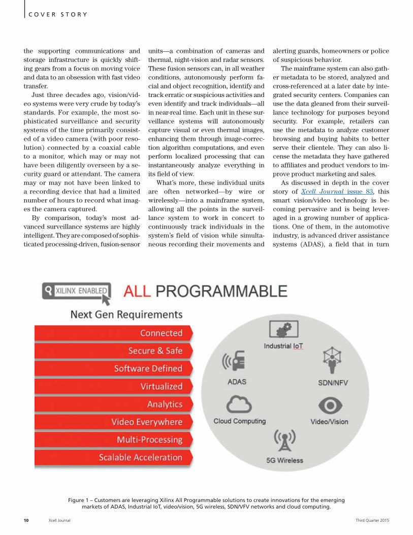
Let’s examine each of these emerging markets and take a look at how they are coming together to enrich our world. Then we’ll take a closer look at how custom-ers are leveraging Xilinx devices and software-defined solutions to create smarter, connected and differentiat-ed systems that in these emerging markets to shape a brilliant future for us all (Figure 1).
IT STARTS WITH VISION Vision systems are everywhere in today’s society. You can find cameras with video capabilities in an ev-er-growing number of electronic systems, from the cheapest mobile phones to the most advanced surgi-cal robots to military and commercial drones and un-manned spacecraft exploring the universe. In concert,
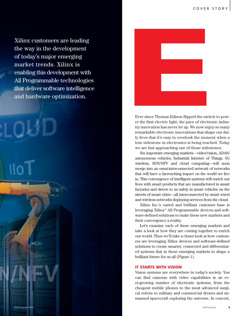
Xilinx customers are leading the way in the development of today’s major emerging market trends. Xilinx is enabling this development with All Programmable technologies that deliver software intelligence and hardware optimization. E
C O V E R S T O R Y
10 Xcell Journal Third Quarter 2015
the supporting communications and storage infrastructure is quickly shift-ing gears from a focus on moving voice and data to an obsession with fast video transfer.
Just three decades ago, vision/vid-eo systems were very crude by today’s standards. For example, the most so-phisticated surveillance and security systems of the time primarily consist-ed of a video camera (with poor reso-lution) connected by a coaxial cable to a monitor, which may or may not have been diligently overseen by a se-curity guard or attendant. The camera may or may not have been linked to a recording device that had a limited number of hours to record what imag-es the camera captured.
By comparison, today’s most ad-vanced surveillance systems are highly intelligent. They are composed of sophis-ticated processing-driven, fusion-sensor
alerting guards, homeowners or police of suspicious behavior.
The mainframe system can also gath-er metadata to be stored, analyzed and cross-referenced at a later date by inte-grated security centers. Companies can use the data gleaned from their surveil-lance technology for purposes beyond security. For example, retailers can use the metadata to analyze customer browsing and buying habits to better serve their clientele. They can also li-cense the metadata they have gathered to affiliates and product vendors to im-prove product marketing and sales.
As discussed in depth in the cover story of Xcell Journal issue 83, this smart vision/video technology is be-coming pervasive and is being lever-aged in a growing number of applica-tions. One of them, in the automotive industry, is advanced driver assistance systems (ADAS), a field that in turn
units—a combination of cameras and thermal, night-vision and radar sensors. These fusion sensors can, in all weather conditions, autonomously perform fa-cial and object recognition, identify and track erratic or suspicious activities and even identify and track individuals—all in near-real time. Each unit in these sur-veillance systems will autonomously capture visual or even thermal images, enhancing them through image-correc-tion algorithm computations, and even perform localized processing that can instantaneously analyze everything in its field of view.
What’s more, these individual units are often networked—by wire or wirelessly—into a mainframe system, allowing all the points in the surveil-lance system to work in concert to continuously track individuals in the system’s field of vision while simulta-neous recording their movements and
Figure 1 – Customers are leveraging Xilinx All Programmable solutions to create innovations for the emerging markets of ADAS, Industrial IoT, video/vision, 5G wireless, SDN/VFV networks and cloud computing.
C O V E R S T O R Y
Third Quarter 2015 Xcell Journal 11
is advancing via processing to enable autonomous vehicles. Advanced vi-sion technology is being further lever-aged in smart factories, smart medical equipment, transportation infrastruc-ture and even in smart cities—all emerging sectors of the Industrial In-ternet of Things (IIoT) market.
ADAS’ DRIVE TO AUTONOMOUS VEHICLES If you own or have ridden in an automo-bile built in the last decade, chances are you have already experienced the value of ADAS technology. Indeed, perhaps some of you wouldn’t be here to read this article if ADAS hadn’t advanced so rapidly. The aim of ADAS is to make drivers more aware of their surround-ings and thus better, safer drivers. The very first of these ADAS tech-nologies was rear-view warning. The earliest versions used a radar sensor connected to an automobile’s central electronic control unit (ECU). When a driver placed the vehicle in reverse, the system sounded a warning if the sensor
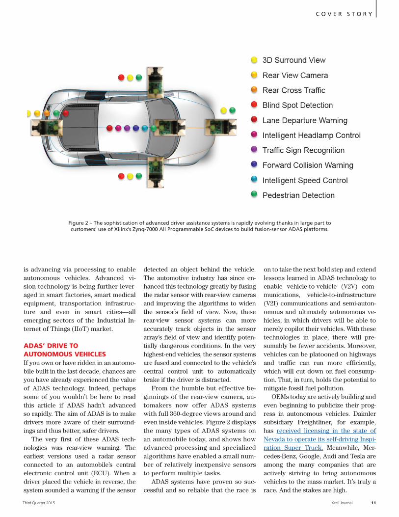
Figure 2 – The sophistication of advanced driver assistance systems is rapidly evolving thanks in large part to customers’ use of Xilinx’s Zynq-7000 All Programmable SoC devices to build fusion-sensor ADAS platforms.
detected an object behind the vehicle. The automotive industry has since en-hanced this technology greatly by fusing the radar sensor with rear-view cameras and improving the algorithms to widen the sensor’s field of view. Now, these rear-view sensor systems can more accurately track objects in the sensor array’s field of view and identify poten-tially dangerous conditions. In the very highest-end vehicles, the sensor systems are fused and connected to the vehicle’s central control unit to automatically brake if the driver is distracted. From the humble but effective be-ginnings of the rear-view camera, au-tomakers now offer ADAS systems with full 360-degree views around and even inside vehicles. Figure 2 displays the many types of ADAS systems on an automobile today, and shows how advanced processing and specialized algorithms have enabled a small num-ber of relatively inexpensive sensors to perform multiple tasks.
ADAS systems have proven so suc-cessful and so reliable that the race is
on to take the next bold step and extend lessons learned in ADAS technology to enable vehicle-to-vehicle (V2V) com-munications, vehicle-to-infrastructure (V2I) communications and semi-auton-omous and ultimately autonomous ve-hicles, in which drivers will be able to merely copilot their vehicles. With these technologies in place, there will pre-sumably be fewer accidents. Moreover, vehicles can be platooned on highways and traffic can run more efficiently, which will cut down on fuel consump-tion. That, in turn, holds the potential to mitigate fossil fuel pollution.
OEMs today are actively building and even beginning to publicize their prog-ress in autonomous vehicles. Daimler subsidiary Freightliner, for example, has received licensing in the state of Nevada to operate its self-driving Inspi-ration Super Truck. Meanwhile, Mer-cedes-Benz, Google, Audi and Tesla are among the many companies that are actively striving to bring autonomous vehicles to the mass market. It’s truly a race. And the stakes are high.
C O V E R S T O R Y
12 Xcell Journal Third Quarter 2015
The challenges for introducing fully autonomous vehicles involve ensuring the vehicles are aware of their locations and their surroundings. They must be able, in real time, to act accordingly as road conditions change second by sec-ond to ensure the safety of those in and around the vehicle. How best to do this given that not all vehicles on the road will have autonomous-driving capabili-ties is a question industry and govern-ments are debating. The answers will undoubtedly fall to safety standards for smart communications between vehi-cles and more forward-looking commu-nications between vehicles and civic in-frastructure. Advances in the emerging realm of the Industrial IoT will help to create this infrastructure.
IIOT’S EVOLUTION TO THE FOURTH INDUSTRIAL REVOLUTION The term Internet of Things has received much hype and sensationalism over the last 20 years—so much so that to many, “IoT” conjures up images of a smart re-frigerator that notifies you when your milk supply is getting low and the wear-able device that receives the “low-milk” notification from your fridge while also fielding texts, tracking your heart rate and telling time. These are all nice-to-have, convenience technologies.
But to a growing number of people, IoT means a great deal more. In the last couple of years, the industry has divid-ed IoT into two segments: consumer IoT for convenience technologies (such as nifty wearables and smart refrigera-tors), and Industrial IoT (IIoT), a bur-geoning market opportunity addressing
and enabling some truly major, substan-tive advances in society.
In Germany, the manufacturing sec-tor of Industrial IoT is seen as such a critical market that the government is actively sponsoring IIoT develop-ment. In a German government effort called Industry 4.0, companies are combining processing, sensor fusion and connectivity to create machine in-telligence for cyber-physical systems (CPS) for factories, hospitals and civ-ic infrastructure. The result will be the enabling of the fourth industrial revo-lution (Figure 3). German companies alone expect to spend $44 billion per year on the CPS retooling, and coun-tries like China, Taiwan and India—all known for manufacturing—will need to follow suit to stay competitive.
CPS designs employ smart architec-tures equipped with fusion sensors sim-ilar to those used in ADAS. The smart, fusion-sensor-based control units in today’s most advanced factories can quickly spot defects in products as they whirl along assembly lines and remove the faulty items. Factories use smart control systems to create virtual bar-riers that spot unsafe conditions for workers. Companies have networked these sensors with the machines in the factory to shut down machinery instant-ly if a worker comes too close to dan-gerous parts of the equipment.
Smart sensor systems of today also monitor the wear of factory motors and parts. Sensors are networked with factory control centers and enterprise systems to help companies perform and optimally schedule equipment
maintenance and preorder parts that they’ll need to replace. In turn, they can schedule factory downtime to perform multiple repairs at once to increase fac-tory efficiency and productivity, and ul-timately to maximize profitability.
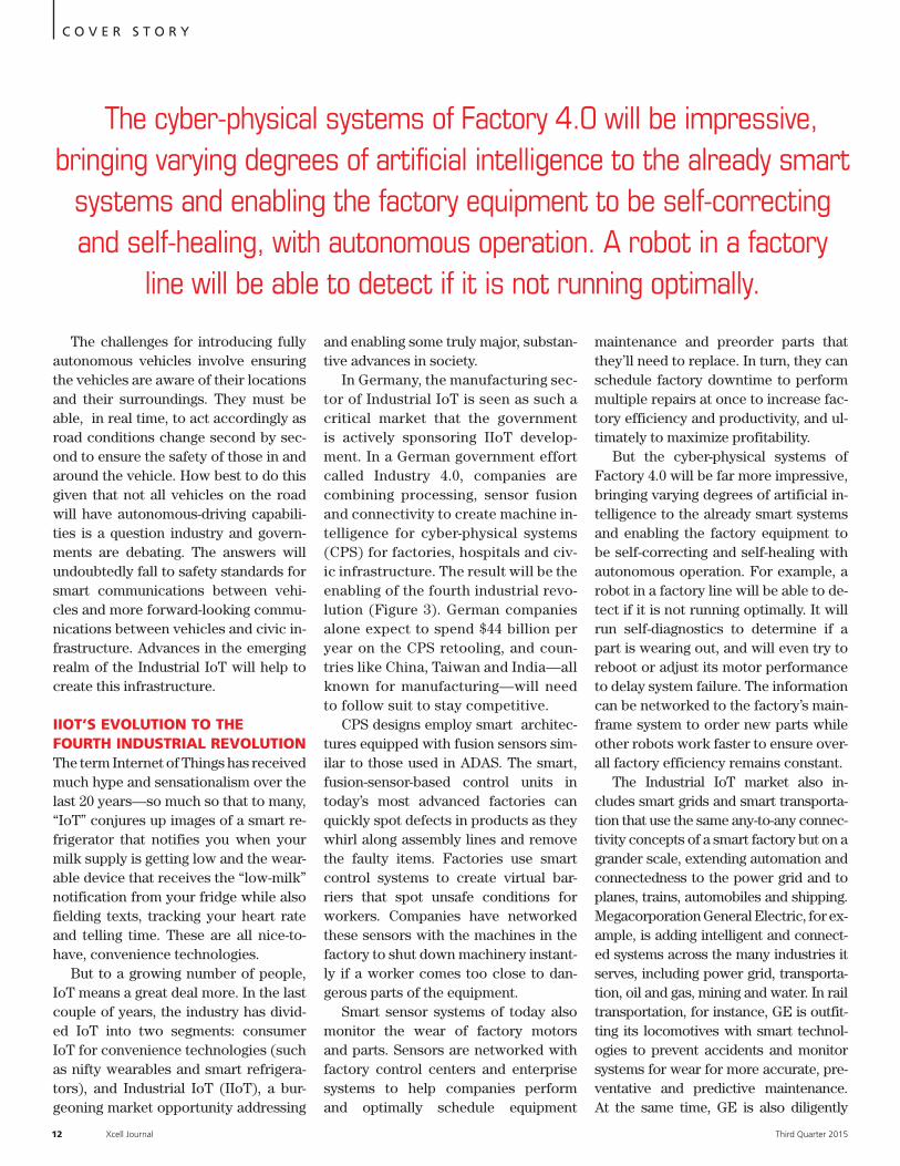
But the cyber-physical systems of Factory 4.0 will be far more impressive, bringing varying degrees of artificial in-telligence to the already smart systems and enabling the factory equipment to be self-correcting and self-healing with autonomous operation. For example, a robot in a factory line will be able to de-tect if it is not running optimally. It will run self-diagnostics to determine if a part is wearing out, and will even try to reboot or adjust its motor performance to delay system failure. The information can be networked to the factory’s main-frame system to order new parts while other robots work faster to ensure over-all factory efficiency remains constant.
The Industrial IoT market also in-cludes smart grids and smart transporta-tion that use the same any-to-any connec-tivity concepts of a smart factory but on a grander scale, extending automation and connectedness to the power grid and to planes, trains, automobiles and shipping. Megacorporation General Electric, for ex-ample, is adding intelligent and connect-ed systems across the many industries it serves, including power grid, transporta-tion, oil and gas, mining and water. In rail transportation, for instance, GE is outfit-ting its locomotives with smart technol-ogies to prevent accidents and monitor systems for wear for more accurate, pre-ventative and predictive maintenance. At the same time, GE is also diligently
The cyber-physical systems of Factory 4.0 will be impressive, bringing varying degrees of artificial intelligence to the already smart
systems and enabling the factory equipment to be self-correcting and self-healing, with autonomous operation. A robot in a factory
line will be able to detect if it is not running optimally.

Third Quarter 2015 Xcell Journal 13
C O V E R S T O R Y
building smart rail infrastructure equip-ment that it has networked with its loco-motives. This allows railway operators to efficiently run their lines and schedule maintenance accordingly to keep freight and passengers moving efficiently, again maximizing operator profitability.
On an even grander scale, variations of these smart-infrastructure technol-ogies are now being integrated in the IIoT market segment called smart cities, which is projected to be a $400 billion in-dustry globally by 2020. As you will read in a contributed article in this issue, the city of Bristol, England, is currently un-dertaking a project that offers a peek into the cities of tomorrow. The project is in-tegrating disparate networks for city san-itation and maintenance, traffic and grid management, and emergency services along with business and personal com-
Figure 3 – Industry 4.0 is the evolution from embedded systems to cyber-physical systems that, through advanced processing, enable smart manufacturing, infrastructure and cities. The result will likely be the world’s fourth industrial revolution.
munications to create a truly connect-ed, intelligent city. To do so, the Bristol Is Open project is heavily leveraging the newest, open, yet secure network topolo-gies, enabling companies wishing to cre-ate solutions for smart cities to connect their networks to Bristol Is Open’s master network. Hamburg, Chicago and Tokyo are among the many other municipalities worldwide that are actively engaging in smart-city development.
The emerging trends toward soft-ware-defined networking (SDN) and network function virtualization (NFV) in wired communications, along with the advent of 5G wireless technologies, are seen as key to enabling further growth of smart-city and other Industrial IoT mar-ket sectors in this mass electronic-sys-tems convergence as network traffic grows exponentially in the coming years.
INTERCONNECTING EVERYTHING TO EVERYTHING ELSE In response to the need for better, more economical network topologies that can efficiently and affordably ad-dress the explosion of data-based ser-vices required for online commerce and entertainment as well as the many emerging IIoT applications, the com-munications industry is rallying be-hind two related network topologies: software-defined networks and net-work function virtualization.
Traditional wired networks have been based on fairly rigid and pro-prietary hardware with limited pro-grammability and versatility. SDN at-tempts to add greater flexibility into network administration by decoupling the top-level control plane functions, which decide where data will be sent,
C O V E R S T O R Y
14 Xcell Journal Third Quarter 2015
from the lower-level data plane func-tions such as routers and switches—the devices that actually forward data to the selected destination. A soft-ware-programmable abstraction layer between the control and data planes allows operators to provision new ap-plications in software, prioritize and optimize where data is delivered in the control plane and deliver that data on existing proprietary hardware (or, with NFV added, via vendor-neutral hard-ware) that operators can scale with changing service requirements.
NFV approaches enable companies to further optimize data plane function-
ality. By virtualizing in software what would typically be the job of very ex-pensive specialized hardware (routers and switches), NFV makes it possible to run the software-derived virtualized functions on less expensive, more gen-eral-purpose hardware (personal serv-ers and commercial data centers). NFV enables network hardware resources to expand economically and, with SDN added, scale on demand and as needed as traffic loads increase and decrease around the world.
On the wireless communications front, 5G promises to reach new data rate heights that will not only enable faster data downloads and streaming video for handset users, but will also provide bandwidth increases that will facilitate the convergence of IIoT and smart-city applications. The wireless
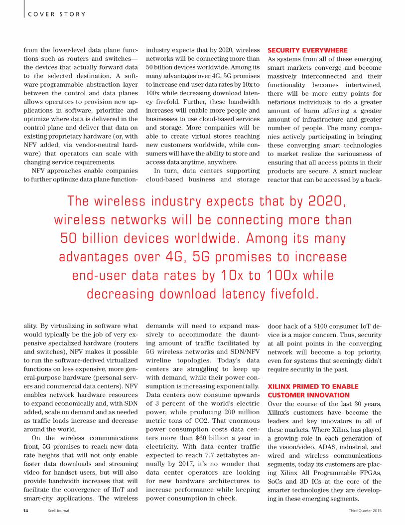
industry expects that by 2020, wireless networks will be connecting more than 50 billion devices worldwide. Among its many advantages over 4G, 5G promises to increase end-user data rates by 10x to 100x while decreasing download laten-cy fivefold. Further, these bandwidth increases will enable more people and businesses to use cloud-based services and storage. More companies will be able to create virtual stores reaching new customers worldwide, while con-sumers will have the ability to store and access data anytime, anywhere.
In turn, data centers supporting cloud-based business and storage
demands will need to expand mas-sively to accommodate the daunt-ing amount of traffic facilitated by 5G wireless networks and SDN/NFV wireline topologies. Today’s data centers are struggling to keep up with demand, while their power con-sumption is increasing exponentially. Data centers now consume upwards of 3 percent of the world’s electric power, while producing 200 million metric tons of CO2. That enormous power consumption costs data cen-ters more than $60 billion a year in electricity. With data center traffic expected to reach 7.7 zettabytes an-nually by 2017, it’s no wonder that data center operators are looking for new hardware architectures to increase performance while keeping power consumption in check.
SECURITY EVERYWHERE As systems from all of these emerging smart markets converge and become massively interconnected and their functionality becomes intertwined, there will be more entry points for nefarious individuals to do a greater amount of harm affecting a greater amount of infrastructure and greater number of people. The many compa-nies actively participating in bringing these converging smart technologies to market realize the seriousness of ensuring that all access points in their products are secure. A smart nuclear reactor that can be accessed by a back-
door hack of a $100 consumer IoT de-vice is a major concern. Thus, security at all point points in the converging network will become a top priority, even for systems that seemingly didn’t require security in the past.
XILINX PRIMED TO ENABLE CUSTOMER INNOVATION Over the course of the last 30 years, Xilinx’s customers have become the leaders and key innovators in all of these markets. Where Xilinx has played a growing role in each generation of the vision/video, ADAS, industrial, and wired and wireless communications segments, today its customers are plac-ing Xilinx All Programmable FPGAs, SoCs and 3D ICs at the core of the smarter technologies they are develop-ing in these emerging segments.
Third Quarter 2015 Xcell Journal 15
The wireless industry expects that by 2020, wireless networks will be connecting more than 50 billion devices worldwide. Among its many advantages over 4G, 5G promises to increase
end-user data rates by 10x to 100x while decreasing download latency fivefold.

C O V E R S T O R Y
Third Quarter 2015 Xcell Journal 15
Xilinx for smarter vision/videoWith a rich history in space exploration, mil-aero and security systems, Xilinx has long served the market with sophisticat-ed vision and video platforms as well as the intellectual property (IP) and meth-odologies to help customers build smart video/vision systems.
Customers are using Xilinx All Pro-grammable FPGAs and SoCs in their vision platforms for real-time analytics to create ADAS systems with high-ve-locity object detection/recognition; clinically precise imaging systems that help surgeons guide robotic instru-ments with pinpoint accuracy; and UAVs and surveillance systems that have instantaneous friend-vs.-foe rec-ognition and tracking.
With the soon-to-arrive 16-nano-meter Zynq® UltraScale+™ MPSoC boasting a total of seven onboard pro-cessing cores (quad-core ARM® Cor-tex®-A53, dual-core Cortex-R5 and a Mali GPU core), Xilinx customers will be able to create even more intelli-gent and highly integrated video sys-tems, speeding up ADAS’ push toward autonomous vehicles and Industrial IoT’s drive to Industry 4.0 factories and smart-city infrastructure.
From ADAS to autonomous vehiclesIn the early 2000s, Xilinx added au-tomotive-grade variants to its FPGA product portfolio. Ever since then, automotive customers have given Xil-inx devices a growing role in their ef-forts to enrich the driving experience through electronics.
The automotive industry has gone through a remarkable renaissance of quality, safety and reliability thanks to electronics. For many decades, automo-tive electronics largely consisted of wire harnesses connecting lights and radios to a battery and an alternator. Then, in the early 2000s, OEMs began using electronic control units to replace highly unreliable mechanical actuators. Every year since then, OEMs have added more advanced electronics to their vehicle lines. What’s more, the development cycles for bring-
ing these innovations to consumers have shortened, thanks in large part to the wide use of Xilinx All Programmable de-vices. Xilinx devices made their debut in automotive infotainment systems but are now making a definitive mark in ADAS.
Today, Xilinx’s Zynq-7000 All Pro-grammable SoC is fast becoming the de facto platform provider for advanced ADAS systems. Audi, Mercedes-Benz, BMW, Ford, Chrysler, Honda, Mazda, Nissan, Toyota, Acura and Volkswagen are among the OEMS using Zynq SoCs or other Xilinx All Programmable devic-es in their ADAS systems. The Zynq SoC serves as a multicamera, multifeature driver assist platform, a high-resolution video and graphics platform, a vehicle networking and connectivity platform and an image-processing and recogni-tion platform. Customers implement algorithms for their design’s most com-plex and compute-intensive functions in the logic portion of the Zynq SoC and use the onboard ARM processing system for serial processing.
With its seven processors, Xilinx’s new Zynq Ultrascale+ MPSoC is destined to provide even more fuel for innova-tion as OEMs drive toward semi-auton-omous and fully autonomous vehicles. With 64-bit application processors, re-al-time processors, a graphics proces-sor, on-chip memory and FPGA logic all on the same device, OEMs can create ever-more-sophisticated fusion systems including V2V communications. What’s more, IIoT smart infrastructure and smart cities can leverage these same Zynq MPSoC platforms for V2X. The in-nate programmability ensures the V2V and V2I networks will scale as the stan-dards evolve and as more autonomous vehicles enter the roadways.
Enabling cyber-physical systems for IIoT Customers in the industrial market have greatly advanced factory efficiency and safety over the last two decades using Xil-inx devices. Today, with Xilinx’s All Pro-grammable FPGAs and SoCs, customers in all the major segments of IIoT are build-
ing secure and safe standards-compliant smart platforms with sensor fusion, smart motion/motor control and smarter and faster enterprise connectivity. These All Programmable platforms are the underly-ing technology for smart wind farms com-posed of many smart wind turbines, each of which can adapt to changing weather conditions for maximum efficiency. The turbines are connected to control and en-terprise systems that monitor wear and schedule preventative maintenance so as to avoid entire-system malfunctions.
With the greater capacity, function-ality and processing clout of Ultra- Scale™ and UltraScale+ devices, Xil-inx’s IIoT customers will be able to advance these smart platforms even further, endowing them with greater intelligence for next-generation cy-ber-physical systems. With the Zynq MPSoC’s seven processors, for exam-ple, customers will be able to integrate more sensor and motor/motion con-trol functions into a single device and achieve real-time response not possible with any other ASSP-plus-FPGA con-figuration. The Zynq MPSoC’s on-chip processing and logic will enable im-proved self-monitoring and diagnostics functionality. Equipment will employ self-healing algorithms or partial recon-figuration to optimize performance as machine conditions change or demand ebbs and flows. What’s more, the Zynq Ultrascale+ MPSoC can work in harmo-ny with Zynq SoC-based systems.
In smart-city applications, compa-nies can use Zynq SoC-based smart-sen-sor systems at the edge of the smart city’s surveillance network to enhance camera resolution and perform object detection and real-time threat analysis. Then, they can turn to the Zynq Ultra- Scale+ MPSoC to synchronize the data received from each Zynq SoC-based smart sensor and communicate it ac-cordingly with traffic control or author-ities as threats, odd behavior, accidents or congestion are detected.
Likewise in the factory, in addition to being at the heart of cyber-physical systems, the Zynq Ultrascale+ MPSoC
C O V E R S T O R Y
16 Xcell Journal Third Quarter 2015
can function as the macro controller of a factory network of Zynq SoC-based motor control, motion control and fusion factory-line quality and safety systems. Companies can leverage the seven processors to coordinate real- time response and analysis received from the Zynq SoC control system. At the same time, they can perform meta-data analysis and communicate it with the enterprise through proprietary net-works (in full compliance with safety and reliability standards) and through emerging high-speed 5G wireless and SDN/NFV wired networks.
Xilinx for 5G, SDN/NFV and cloud computingXilinx’s devices have played a signifi-cant role in every buildout of the wire-less and wired networking infrastruc-ture since the 1980s. With every cycle of Moore’s Law, Xilinx devices have grown in capacity and functionality to the point where today’s All Programmable devices enable design teams to innovate new networking systems with the high-est level of system programmability and differentiation ever seen.
With Xilinx’s 7 series, 20nm Ultra- Scale and upcoming 16nm UltraScale+
devices, Xilinx is enabling custom-ers today to quickly bring to the mar-ket 5G and SDN/NFV infrastructure equipment with the highest degree of programmability. Xilinx’s All Pro-grammable FPGAs, SoCs and 3D ICs are the most flexible platforms for the evolving software and hardware re-quirements of 5G and SDN/NFV. Fur-ther, they are the ideal programmable solution for the performance-per-watt demands of data center systems at the heart of the cloud computing business, poised to expand rapidly with 5G and SDN/NFV networking.
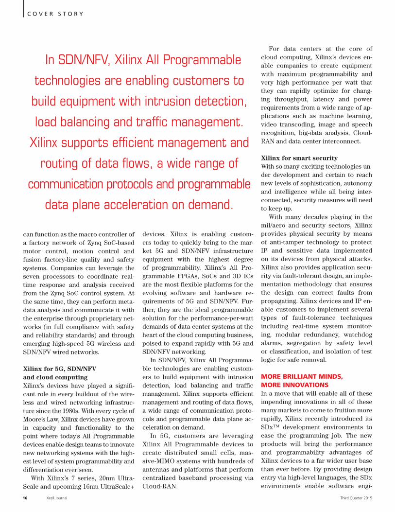
In SDN/NFV, Xilinx All Programma-ble technologies are enabling custom-ers to build equipment with intrusion detection, load balancing and traffic management. Xilinx supports efficient management and routing of data flows, a wide range of communication proto-cols and programmable data plane ac-celeration on demand.
In 5G, customers are leveraging Xilinx All Programmable devices to create distributed small cells, mas-sive-MIMO systems with hundreds of antennas and platforms that perform centralized baseband processing via Cloud-RAN.
For data centers at the core of cloud computing, Xilinx’s devices en-able companies to create equipment with maximum programmability and very high performance per watt that they can rapidly optimize for chang-ing throughput, latency and power requirements from a wide range of ap-plications such as machine learning, video transcoding, image and speech recognition, big-data analysis, Cloud-RAN and data center interconnect.
Xilinx for smart security With so many exciting technologies un-der development and certain to reach new levels of sophistication, autonomy and intelligence while all being inter-connected, security measures will need to keep up.
With many decades playing in the mil/aero and security sectors, Xilinx provides physical security by means of anti-tamper technology to protect IP and sensitive data implemented on its devices from physical attacks. Xilinx also provides application secu-rity via fault-tolerant design, an imple-mentation methodology that ensures the design can correct faults from propagating. Xilinx devices and IP en-able customers to implement several types of fault-tolerance techniques including real-time system monitor-ing, modular redundancy, watchdog alarms, segregation by safety level or classification, and isolation of test logic for safe removal.
MORE BRILLIANT MINDS, MORE INNOVATIONS In a move that will enable all of these impending innovations in all of these many markets to come to fruition more rapidly, Xilinx recently introduced its SDx™ development environments to ease the programming job. The new products will bring the performance and programmability advantages of Xilinx devices to a far wider user base than ever before. By providing design entry via high-level languages, the SDx environments enable software engi-
Third Quarter 2015 Xcell Journal 17
In SDN/NFV, Xilinx All Programmable
technologies are enabling customers to
build equipment with intrusion detection,
load balancing and traffic management.
Xilinx supports efficient management and
routing of data flows, a wide range of
communication protocols and programmable
data plane acceleration on demand.
C O V E R S T O R Y
Third Quarter 2015 Xcell Journal 17
neers and system architects to pro-gram Xilinx devices with languages they are accustomed to using (see cov-er story, Xcell Journal issue 91). Soft-ware engineers outnumber hardware engineers worldwide 10 to 1.
To enable further innovation in SDN, Xilinx’s new SDNet™ software-defined environment lets systems engineers build programmable data plane solu-tions with a high-level language to meet a network’s unique performance and latency requirements. To fuel further innovation in NFV and other network architectures and topologies, develop-ers can use Xilinx’s SDAccel™ environ-ment, which enables system and soft-ware engineers to program the logic in
Xilinx FPGAs in C, C++ and OpenCL™ to accelerate the performance of virtu-alized network functions (VNFs).
To enable further innovation in vid-eo/vision, ADAS/autonomous vehicles and IIoT applications that call for em-bedded processing, Xilinx’s SDSoC™ development environment allows soft-ware and system engineers to create entire systems in C++. They can op-timize system performance by having the environment’s compiler implement slower functions in the Zynq SoC’s or MPSoC’s logic blocks. In this way, ar-chitects and software engineers can create systems with optimum perfor-mance and functionality that simply isn’t achievable in two-chip platforms.
As we are fast approaching the mile-stone where video/vision, ADAS/auton-omous vehicles, IIoT, 5G wireless, SDN/NFV and cloud computing converge, we are certain to see a number of innovations that will drastically change the society we live in—hopefully for the better. Today, we are at the early stages of all these in-novations, and Xilinx is well equipped to help customers bring their brilliant prod-ucts to market. In the following pages in this special issue of Xcell Journal, you will get a small sampling of the many exciting innovations Xilinx customers are creating in these emerging markets and a peek at how they are leveraging Xilinx’s All Pro-grammable solutions today to make them a reality for us all…very soon.
Debugging Xilinx's ZynqTM -7000 family with ARM® CoreSightTM
► RTOS support, including Linux
kernel and process debugging
► SMP/AMP multicore Cortex®- A9
MPCoreTMs debugging
► Up to 4 GByte realtime trace
including PTM/ITM
► Profiling, performance and
statistical analysis of ZynqTM's
multicore Cortex®-A9 MPCoreTM
X C E L L E N C E I N S M A R T C I T I E S
18 Xcell Journal Third Quarter 2015
World’s First Programmable City Arises, Built on Xilinx FPGAs by Bijan R. Rofoee Senior Network EngineerBristol Is Open [email protected]
Mayur Channegowda Chief Scientist, SDNZeetta Networkswww.zeetta.com
Shuping Peng Research FellowUniversity of BristolChief Scientist, VirtualizationZeetta Networks
George Zervas Professor of High-Performance NetworksUniversity of Bristol
Dimitra Simeonidou CTO, Bristol Is Open Professor of High-Performance NetworksUniversity of Bristol

X C E L L E N C E I N S M A R T C I T I E S
Third Quarter 2015 Xcell Journal 19
By 2050, the human popu-lation will have reached 9 billion people, with 75 percent of the world’s inhabitants living in cit-ies. With already around
80 percent of the United Kingdom’s population living in urban areas, the U.K. needs to ensure that cities are fit for purpose in the digital age. Smart cit-ies can help deliver efficiency, sustain-ability, a cleaner environment, a higher quality of life and a vibrant economy.
To this end, Bristol Is Open (BIO) is a joint venture between the University of Bristol and Bristol City, with collabo-rators from industry, universities, local communities, and local and national governments. Bristol Is Open (www.bristolisopen.com) is propelling this municipality of a half million people in southwest England to a unique status as the world’s first programmable city.
Bristol will become an open testing ground for the burgeoning new market of the Industrial Internet of Things—that is, the components of the smart-city infrastructure. The Bristol Is Open proj-ect leverages Xilinx® All Programmable FPGA devices in many areas of develop-ment and deployment.
THE VISION OF THE SMART CITY A smart city utilizes information and communications networks along with Internet technologies to address ur-ban challenges, with the objective of dramatically improving livability and resource sustainability. It is predicted [1] that the smart-cities industry will value more than $400 billion global-ly by 2020, with the U.K. expected to gain at least a 10 percent share, or $40 billion. The U.K. government invest-
Bristol, England, has become a testbed for smart-city technologies. The Bristol Is Open project is a living experiment in the evolution of the Internet of Things.
ment in the smart-city sector includes around $150 million for research into smart cities funded by Research Coun-cils U.K.; $79 million over five years earmarked for the new Future Cities Catapult center being established by the Technology Strategy Board in London; $52 million invested in future city demonstrators earlier this year; and $63 million recently allocated to Internet of Things (IoT) research and demonstrator projects.
Bristol Is Open is leading the way to building a city-scale research and innovation testbed. The aim is to drive digital innovation for the smart cities of the future: the open and programmable communities that will be the norm in the latter part of the 21st century.
The BIO testbed is equipped with leading-edge programmable networking technologies, enabled by a citywide op-erating system called NetOS, that allow smart-city applications to interact with city infrastructure—to program, virtual-ize and tailor network functions for op-timum performance. Xilinx devices as high-performance generic platforms are utilized at many points in the city from the wired, wireless and IoT networking infrastructure to emulation facilities.
Let’s take a tour of this new type of urban community, starting with the overall vision for programmable cit-ies. Then we will take a deeper look at how the Bristol project is utilizing Xilinx devices to build urban “white boxes” and to deliver various net-working functions.
FUTURE SMART CITIES More than 100 cities of 1 million people will be built in the next 10 years world-wide [2], while the continuous influx of
people to cities will grow the number of urban residents by 60 million every year during that decade. [2] The result is that more than 70 percent of the world’s pop-ulation will be living in cities by 2050. Considering also that cities occupy just 2 percent of the world’s landmass while consuming about three-quarters of its re-sources, the ongoing urbanization pres-ents economic and societal challenges and a strain on the urban infrastructure. Growing cities will have to deal with a variety of challenges to maintain eco-nomic advancement, environmental sus-tainability and social resiliency.
The solution is to make cities smart-er. Although there is no absolute defini-tion for smart cities, there are a number of key aspects widely recognized [3] for a smart city’s operations. They include:
• Citizen-centric service delivery, which involves placing the citizen’s needs at the forefront.• Transparency of outcomes/perfor- mance to enable citizens to com- pare and critique performance, establishment by establishment and borough by borough.• An intelligent physical infrastruc- ture, enabling service providers to manage service delivery, data gathering and data analyzing effectively. • A modern digital, secure and open software infrastructure, to allow citizens to access the information they need, when they need it.
Technological enablers for smart cities are inspired by the Internet of Things, a market that, according to Gartner, [4] will grow to 26 billion units installed as of 2020. That total rep-resents an almost thirtyfold increase from 0.9 billion in 2009, with the rev-enue from technologies and services exceeding $300 billion. Smart cities de-ploy IoT technologies on a wide scale, enabling data gathering from sensors and things present in the ecosystem, pushing them for analysis and feeding back commands to actuators, which will control city functions.
X C E L L E N C E I N S M A R T C I T I E S
20 Xcell Journal Third Quarter 2015
From sensing and analysis, infor-mation passes back to actuators in the city infrastructure to control op-erations dynamically. This arrange-ment is an enabler for driverless cars using smart transport facilities; great-er power efficiency thanks to smart lighting; the management of network resources for different times (daily and seasonal changes); the movement of resources depending on occasions such as sports events, which require high-quality broadcast and coverage; and efficient handling of emergency situations (city evacuation).
PROGRAMMABLE CITY VS. SMART CITY Smart cities aim to improve and en-hance public and private service offer-ings to citizens in a more efficient and cost-effective way by exploiting net-work, IT and, increasingly, cloud tech-nologies. To achieve this goal, smart cities rely extensively on data collected from citizens, the environment, vehicles and basically all the “things” present in the city. The more data that becomes available, the more accurately city op-erations can be analyzed, which in turn will lead to the design and availability of smart-city services.
For the network infrastructure, city-wide data retrieval and processing mean massive amounts of sensor data that needs to be collected, aggregated and transferred to computational facilities (data centers) for storage and possibly processing. The wide diversity of sce-narios and applications presents major challenges regarding networking and computing infrastructure requirements in smart cities. Legacy information and communications technology (ICT) ur-ban infrastructure can be a major bot-tleneck for smart-city operations, as it does not offer the capacity, flexibility and scalability desirable for the emerg-ing, future-proof, resource-demanding and scalable smart-city applications.
Programmable networking technolo-gies offer unique capabilities for raising the performance of smart-city opera-
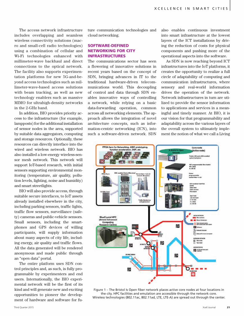
BRISTOL IS OPEN: VISION AND ARCHITECTURE Launched in 2013, Bristol Is Open is a program funded by the local, national and European governments and also by the private sector. BIO is already deliv-ering R&D initiatives that contribute to the advancement of smart cities and the Internet of Things. BIO aims to serve as a living lab—an R&D testbed targeting city-driven digi-tal innovation. It provides a managed multitenancy platform for the develop-ment and testing of new solutions for information and communication infra-structure, and thus forms the core ICT enabling platform for the Future Cities agenda. At the infrastructure level, BIO comprises five distinctive SDN-enabled infrastructures, as shown in Figure 1:
• Active nodes as optoelectronic-net-work white boxes using FPGA programmable platforms and het-erogeneous optical and Layer 2/3 networking infrastructure
• Heterogeneous wireless infrastructure comprising Wi-Fi, LTE, LTE-A and 60-GHz millimeter-wave technologies
• IoT sensor mesh infrastructure
• Network emulator comprising a serv-er farm and an FPGA-SoC-network processor farm
• Blue Crystal high-performance com-puting (HPC) facility
On the metro network, the infra-structure offers access to dynamic opti-cal switching supporting multi-terabit/second data streams, multirate Layer 2 switching (1 to 100 GbE) and Layer 3 routing. The metro is also equipped with programmable hardware plat-forms and high-performance servers to allow open access to the infrastruc-ture and a capability to create and experiment with new hardware and software solutions. This wired part of the infrastructure also connects to the Blue Crystal HPC facilities at Bristol in order to support experimentation with advanced cloud infrastructures.
tions. These technologies exploit open software and hardware platforms, which users can program to tailor network functions for different use case requirements. Improved con-trol, monitoring and resource alloca-tion in the network are the evident benefits of deploying programmable networks. More important, program-mable technologies facilitate the integration of networks with IT fa-cilities, which will result in greater application awareness.
Software-defined networking (SDN) is one of the main enablers for program-mable networks. The SDN foundation is based on decoupling infrastructure control from the data plane, which greatly simplifies network management and application development while also allowing deployment of generic hard-ware in the network for delivering net-working functions.
SDN-based scalable and facilitat-ed network management also greatly empowers network virtualization. Net-work virtualization essentially enables multiple users to operate over shared physical resources, isolated from one another, reducing the need for install-ing supplementary physical hardware. Network function virtualization (NFV), a more recent innovation in virtualiza-tion technologies, offers software im-plementation of network functions in commodity hardware. Network func-tions such as firewall, deep packet in-spection, load balancing and so on are deployed as pluggable software con-tainers in generic machines, expedit-ing network service deployments with great cost-efficiency.
In addition to software-driven net-working, hardware and infrastructure programmability will progress beyond fixed-function hardware data planes. Adding high-level programmability and more sophisticated functionality to the data plane, accessed via standard software APIs, will make it possible to manage networking resources more in-telligently and efficiently, increasing the rate of innovation.
X C E L L E N C E I N S M A R T C I T I E S
Third Quarter 2015 Xcell Journal 21
The access network infrastructure includes overlapping and seamless wireless connectivity solutions (mac-ro and small-cell radio technologies) using a combination of cellular and Wi-Fi technologies enhanced with millimeter-wave backhaul and direct connections to the optical network. The facility also supports experimen-tation platforms for new 5G-and-be-yond access technologies such as mil-limeter-wave-based access solutions with beam tracking, as well as new technology enablers such as massive MIMO for ultrahigh-density networks in the 2-GHz band.
In addition, BIO provides priority ac-cess to the infrastructure (for example, lampposts) for the additional installation of sensor nodes in the area, supported by suitable data aggregators, computing and storage resources. Optionally, these resources can directly interface into the wired and wireless network. BIO has also installed a low-energy wireless-sen-sor mesh network. This network will support IoT-based research, with initial sensors supporting environmental mon-itoring (temperature, air quality, pollu-tion levels, lighting, noise and humidity) and smart streetlights.
BIO will also provide access, through suitable secure interfaces, to IoT assets already installed elsewhere in the city, including parking sensors, traffic lights, traffic flow sensors, surveillance (safe-ty) cameras and public-vehicle sensors. Small sensors, including the smart-phones and GPS devices of willing participants, will supply information about many aspects of city life, includ-ing energy, air quality and traffic flows. All the data generated will be rendered anonymous and made public through an “open data” portal.
The entire platform uses SDN con-trol principles and, as such, is fully pro-grammable by experimenters and end users. Internationally, the BIO experi-mental network will be the first of its kind and will generate new and exciting opportunities to pioneer the develop-ment of hardware and software for fu-
ture communication technologies and cloud networking.
SOFTWARE-DEFINED NETWORKING FOR CITY INFRASTRUCTURES The communications sector has seen a flowering of innovative solutions in recent years based on the concept of SDN, bringing advances in IT to the traditional hardware-driven telecom-munications world. This decoupling of control and data through SDN en-ables innovative ways of controlling a network, while relying on a basic data-forwarding operation, common across all networking elements. The ap-proach allows the integration of novel architecture concepts, such as infor-mation-centric networking (ICN), into such a software-driven network. SDN
also enables continuous investment into smart infrastructure at the lowest layers of the ICT installations by driv-ing the reduction of costs for physical components and pushing more of the operational aspects into the software.
As SDN is now reaching beyond ICT infrastructures into the IoT platforms, it creates the opportunity to realize a full circle of adaptability of computing and communication infrastructures, where sensory and real-world information drives the operation of the network. Network infrastructures in turn are uti-lized to provide the sensor information to applications and services in a mean-ingful and timely manner. At BIO, it is our vision for that programmability and adaptability across the various layers of the overall system to ultimately imple-ment the notion of what we call a Living
Figure 1 – The Bristol Is Open fiber network places active core nodes at four locations in the city. HPC facilities and emulation are accessible through the network core.
Wireless technologies (802.11ac, 802.11ad, LTE, LTE-A) are spread out through the center.

X C E L L E N C E I N S M A R T C I T I E S
22 Xcell Journal Third Quarter 2015
SDN principles, will provide the need-ed programmability and adaptability for smart cities. NetOS will be an over-arching and distributed operating sys-tem spanning from terminals (even the more advanced ones, e.g., mobile robots, drones) through the network elements to the cloud/IT resources. This citywide OS will cope with the heterogeneity of un-derlying resources based on a distributed software architecture. NetOS will act as a logical entity that is implemented in a hi-erarchical manner with distributed soft-ware, making it possible to map varied services on the infrastructure.
VIRTUALIZATION FOR CITY INFRASTRUCTURE A large number of highly diverse city applications need to be supported on top of the city infrastructures. For ex-ample, some applications will demand high capacity and very low latency. Oth-ers will consume very little bandwidth but will need to support a very large number of endpoints. Still others will have strict requirements on resiliency or security, privacy and so on.
It is neither feasible nor cost-effective
to establish dedicated infrastructures to support specific applications. Therefore, one of the key challenges for the city infrastructure operators is to offer cus-tomized, application-specific network solutions over a common ICT infrastruc-ture. Virtualization, when integrated with an SDN-enabled control platform, is a key technical enabler for addressing this challenge. Virtualization is able to create multiple coexisting but isolated virtual in-frastructures running in parallel, serving its tenant’s application requirements.
By thorough analysis of each tenant’s requirements in terms of social policy, security and resources, it’s possible to construct a virtual infrastructure with a certain network topology, indicating the way that virtual nodes are interconnect-ed with virtual links. Performance pa-rameters (for example, latency) and re-source requirements (such as network bandwidth, compute CPU/memory) are specified in the virtual nodes and links. Generally, virtual resources (nodes and links) are obtained by partitioning or aggregating physical resources. There-fore, a programmable hardware infra-structure is essential to support the
OPEN DATAPLATFORM
SOFTWARE DEFINED NETWORKCITY OPERATING SYSTEM
CITY NETWORK(S)
PLATFORM VIRTUALIZATION/SLICING
OpenStack, etc.INFORMATION MODELS
DATA COLLECTION ENGINE sync async
MULTIPLE SENSORS/PLATFORMS & HARDWARE
SDN controller
gw/drv gw/drv gw/drv gw/drv gw/drv gw/drv gw/drv gw/drv gw/drv
DATA PRE-PROCESSING SERVICES srv1 srvN
Figure 2 – NetoOS is an SDN-based platform, built in a multilayer structure, which can communicate with networking, IT and IoT technologies. This platform natively supports data collection, virtualization, information modeling and interfacing with third-party applications.
Network, where the Internet and things truly merge into a coherently managed and operated computing and communi-cation environment.
Demonstrating SDN-based platforms on a citywide scale is crucial. Future Internet and 5G technologies are pres-ent in the BIO testbed, specifically an SDN-enabled optical-backbone infra-structure using current and contempo-rary (i.e., Wi-Fi, LTE, millimeter-wave) radio access technologies. The stimu-lating media and entrepreneurial com-munity is present throughout the BIO testbed (the engine shed in Figure 1 is home to a startup incubator and the wa-tershed is home to the media communi-ty in Bristol). Members of these commu-nities also serve as an excellent set of early-user groups for the use case work. Their involvement in BIO allows us to capture the insights and requirements posed by the municipal communities.
The wired, wireless and RF mesh net-works are technology-agnostic, built on open-network principles using SDN tech-nologies that enable network function virtualization. A city operating system called NetOS (Figure 2), also based on

Third Quarter 2015 Xcell Journal 23
X C E L L E N C E I N S M A R T C I T I E S
composition of virtual infrastructures with high granularity and scalability.
In the city environment, the devices deployed in the urban infrastructure are heterogeneous, including wireless/mo-bile, wired, optical networks, data centers/cloud and functional appliances. In order to enable seamless service provisioning, it’s mandatory to support converged vir-tual infrastructures enhanced with virtual network functions across the multitech-nology, multidomain city infrastructure, so that each tenant can get its own slice of the city infrastructure. However, currently these technology domains are controlled and managed in silos. The NetOS with SDN capabilities at BIO provides a logi-cally centralized control platform that can break through the management silos and bridge the different technology segments. The operating system is able to abstract the heterogeneous city devices, hide their complex technical details and expose the infrastructure in a uniform way.
THE VISION FOR THE WHITE BOX Open network devices, or network white boxes, use unbranded, generic, modular and programmable hardware platforms. This type of equipment can
load customized operating systems and enable on-demand redefining of network functions without the re-strictions of vendor-locked devices. Network processors were the initial route to hardware programmability of the underlying network, leveraging the ease of defining functions through software APIs. Network processors are well-known hardware platforms that provide generic programmable fea-tures similar to general-purpose CPUs (with extended hardware resources), and can be programmed to perform various networking functions. The main advantage of processor-based ar-chitectures is rapid implementation of networking functions using high-level languages such as C, which is highly desirable for rapid prototyping. Net-work processors, however, are not op-timized for parallel operations, which are essential for building high-perfor-mance data plane technologies sup-porting high-data-rate transport.
Field-programmable gate arrays (FPGAs) are high-performance and ge-neric processing platforms utilizing pro-grammability from transistor-level to IP-based function level. This makes them
highly desirable platforms for designing and prototyping network technologies that must demonstrate high degrees of flexibility and programmability.
We are using Xilinx FPGAs that have evolved into system-on-chip (SoC) de-vices in multiple points within the BIO infrastructure: in active nodes (see Fig-ure 2) as optoelectronic white boxes, emulation facilities, wireless LTE-A experimental equipment and IoT plat-forms. BIO uses programmable and customizable network white boxes that consist of programmable electrical (FPGA) and optical (switching, process-ing, etc.) parts. These boxes—which enable high-capacity data processing and transport, function programmability and virtualization—are deeply control-lable through SDN interfaces. Figure 3 demonstrates the FPGA-based platform, which can host multiple functions in a programmable way, and is interfaced to a programmable photonic part. [5]
FPGAs offer several advantages, in-cluding hardware repurposing through function reprogrammability, easier up-gradability and shorter design-to-deploy cycles than those of application-specific standard products (ASSPs).
Figure 3 – Bristol Is Open’s network white box is built around Xilinx FPGAs.

The photonic part of the network white boxes uses an optical backplane on which a number of photonic function blocks are plugged into optical functions such as amplification, multicasting, wave-length/spectrum selection, signal add/drop, etc. Critically, the input and output links are decoupled from any of the func-tions that the node can offer, unlocking flexibility, efficiency and scalability, and minimizing disruptive deployment cycles with on-service hitless repurposing.
ZYNQ SOC-BASED EMULATION PLATFORM To broaden the capabilities of BIO facil-ities in experimenting with larger and more-realistic scenarios, we have de-ployed a network emulator facility with-in BIO. This platform enables network emulation as well as resource virtualiza-tion and virtual-infrastructure composi-tion techniques for advanced network, cloud and computational research. The emulation platform also utilizes local and remote laboratory-based facilities and distributed research infrastructures (networks and computing). Figure 4 demonstrates the multilayer, multiplat-form emulation facilities at the core of the Bristol Is Open infrastructure.
The emulation facility offers a num-ber of functions instrumental for en-hanced network studies in conjunction
with the BIO city network and other re-mote interconnected laboratories:
1. Node and link emulation: This plat-form can emulate network elements such as routers and switches from the wired and wireless domains, along with the interconnecting links with various physical attributes.
2. Protocol emulation: Whether cen-tralized or distributed, network nodes rely on the protocols to communi-cate. The emulation facility with pre-cise modeling of the network technol-ogies allows the user/researcher to try out communication protocols and study their behavior on scale.
3. Traffic emulation: Depending on the emulation scenario (wireless net-works, data center networks, etc.), traffic patterns with arbitrary inter-vals and operating from a few mega-bits to multiple terabits per second can be generated and applied to the target emulated or physical network.
4. Topology emulations: Any topolog-ical formation of the desired nodes and links is possible using the BIO emulation facility. This gives the user a chance to fully examine various aspects of the desired technology on the realistic network topologies be-fore deployment and installation.
Unlike any other existing facilities that offer computer host-based emulation en-vironments, BIO uniquely includes pro-grammable hardware (FPGAs, network processors) as well as dynamic and flex-ible connectivity to multitechnology test-beds and a rich, dedicated connectivity infrastructure. The use of programmable hardware and external interconnectivity will allow users to accurately emulate the functionality and performance of network and computing technologies in scale and use them to synthesize representative complex systems. Exploiting the FPGA’s parallel-processing capabilities and high-speed I/Os, BIO is equipped to emulate current or experimental network tech-nologies and topologies, be they wired or wireless, precisely and at scale.
The network emulator uses a vast amount of advanced networking and IT technologies. An FPGA farm, server farm and L2/L3 programmable network-ing equipment are the main building blocks of the facility, enabling the users to build, experiment with and use vari-ous networking technologies in the data plane and control plane, such as virtual-ization, SDN and NFV, resource/work-load allocation tools and algorithms, etc.
The emulator is connected to the BIO city network through 10-, 40- and 100-Gbps ports. The emulated networks can
X C E L L E N C E I N S M A R T C I T I E S
24 Xcell Journal Third Quarter 2015
Figure 4 – The emulation facility in Bristol Is Open includes programmable hardware in the form of FPGAs and network processors.

use standard data plane protocols such as Ethernet, OTN and Infiniband, or cus-tom and proprietary protocols, to inter-connect with other network domains.
The emulator uses Xilinx’s ARM®-based Zynq®-7000 All Programmable SoC platform, a single-chip implementation of processing and FPGA technologies. Algorithm acceleration is one of the tar-get use cases for the Zynq SoC, where computationally intensive tasks for re-source allocation, path calculation, load balancing and the like are offloaded to FPGA-based parallel processing. Hard-ware-assisted network function virtual-ization is another example of how we use Zynq SoC-based platforms in BIO for run-ning performance-critical virtual network functions (VNFs) such as deep packet inspection, service control and security. Xen-based virtualization of ARM cores
additionally facilitates running multiple operating systems on the same SoC chip. In this way, BIO can let multiple opera-tors host their VNFs on the same device, and have shared and/or dedicated access to the parallel hardware computing re-sources to boost performance.
EXPERIMENTATION AS A SERVICE The way cities work is changing. Using digital technologies, BIO is creating an open, programmable city that gives cit-izens more ways to participate in and contribute to the way their city works. We call it “City Experimentation as a Service.” Being open guides our procurement, our data management and the hardware and the software we use. Being open means the stakeholders in BIO proactively share what we learn with other cities, technolo-gy companies, universities and citizens.
REFERENCES
1. https://www.gov.uk/government/news/uk-set-to-lead-the-way-for-smart-cities
2. UN State of World Cities report, 2012/13,http://www.unhabitat.org/pmss/ listItem-Details.aspx?publicationID=3387
3 https://www.gov.uk/government/up-loads/system/uploads/attachment_data/file/246019/bis-13-1209-smart-cities-back-ground-paper-digital.pdf
4. http://www.gartner.com/newsroom/id/2636073
5. Bijan Rahimzadeh Rofoee, George Zer-vas, Yan Yan, Norberto Amaya and Dimi-tra Simeonidou, “All Programmable andSynthetic Optical Network: Architectureand Implementation,” Journal of OpticalCommunications and Networking 5,1096-1110 (2013)
Third Quarter 2015 Xcell Journal 25
X C E L L E N C E I N S M A R T C I T I E S
FPGA-Based Prototyping for Any Design Size? Any Design Stage? Among Multiple Locations?
That’s Genius!Realize the Genius of Your Design with S2C’s Prodigy Prototyping Platform
Download our white paper at:http://www.s2cinc.com/resource-library/white-papers

X C E L L E N C E I N 5 G
26 Xcell Journal Third Quarter 2015
5G Wireless Brings Ubiquitous Connectivity
As the 5G communications market begins to take shape, wireless equipment manufacturers turn to emulation systems built around Xilinx FPGAs.
by David Squires Vice President of Business DevelopmentBEEcube, A National Instruments Company [email protected]

X C E L L E N C E I N 5 G
Third Quarter 2015 Xcell Journal 27
As wireless operators continue their relentless march to be the first to provide consumers with new services and devices, additional bandwidth and service plans that yield higher profits, infrastructure companies are also racing to field the 5G equipment that will form the foundation of the next generation of wireless commu-nications. To enable this 5G wireless infrastructure, BEEcube (recently acquired by National Instruments) leveraged Xilinx® FPGAs and Zynq®-7000 All Programmable SoCs to pro-vide 5G equipment manufacturers with a new emulation system as well as a mobile-handset emulator. The BEE7 and nanoBEE are enabling design teams to be innovative and productive so they can bring 5G technologies to market ahead of the competition.
Before describing BEEcube’s new FPGA-based products in detail, let’s take a look at the wireless communica-tions industry’s vision of the 5G market and the technical challenges facing it.
THE 5G VISION A key component of the wireless fu-ture will be the widespread deploy-ment of 5G wireless networks. The primary goals of 5G are to support a thousandfold gain in capacity, connec-tions for at least 100 billion devices and 10-Gbps data rates delivered to in-dividual users. Additionally, these new networks will be capable of providing mass low-latency connectivity among people, machines and devices. De-ployment of 5G networks is expected
hardware. Any prototype platform must be capable of scaling to tens of terabits per second, accepting hun-dreds of optical fibers and supporting tens of gigasamples of RF analog data.
The DSP processing power re-quired to implement high-order mod-ulation schemes across many anten-nas and many sectors, as in massive MIMO, is immense. Tens of thousands of multiply-accumulate (MAC) units will be required.
As the complexity of modern commu-nications systems increases, it becomes impossible for all but the very largest OEMs to maintain all of their own intel-lectual property. Having a rich set of IP, including massive MIMO, CPRI, multiple waveforms as well as an LTE-Advanced protocol stack, can dramatically acceler-ate development (see sidebar).
The world’s carriers are all trying to push as much processing as pos-sible into the cloud. This effort lever-ages the scale of data centers and in so doing, drives down the cost of pro-cessing each call. Efficient connec-tion to the cloud requires 10GE, 40GE or PCIe® interfaces.
The programming model must sup-port the major existing design flows of C, C-to-gates, VHDL, Verilog and high-level modeling environments (Lab-VIEW and MATLAB®/Simulink® are the two most popular).
For clocks, the hardware must be capable of extracting embedded clocks from CPRI or synchronous Ethernet, and cleaning up the clocks and main-taining clock jitter of less than 300 fs across racks of gear at ADC sampling frequencies of up to 6 GHz in order to preserve the integrity of informa-tion-dense broadband wireless signals.
To address these challenges, BEEcube has created a powerful new emulation platform called BEE7 that leverages the best-in-class features of Xilinx’s Virtex®-7 FPGAs.
BEE7 PLATFORM ARCHITECTURE The BEE7 platform is a state-of-the-art architecture that BEEcube de-
to commence in 2020; 5G radio access will be built using the next evolution of existing wireless radio access tech-nologies, such as LTE and Wi-Fi, com-bined with entirely new technologies.
While the industry has defined the end goals of 5G, how to actually achieve those goals is the multibillion-dollar question. Many companies worldwide are in the process of developing 5G in-frastructure equipment as well as the many remarkable devices that will com-municate through it.
The detailed technical approaches for 5G are still uncertain; however, sev-eral things are clear. Future wireless systems will use existing bandwidth more efficiently by exploiting spa-tial diversity through massive MIMO, beam forming and related techniques. New allocations of spectrum will be dedicated to cellular, adding to the overall channel capacity. Higher user throughput will be achieved, mainly through carrier aggregation and new frequency bands. The density of urban cell sites will increase, simultaneous-ly reducing power requirements and allowing much higher spectral reuse within a given area. The core network will make increased use of the cloud for both data and control purposes.
Since 5G standards have not yet been set, those companies that can demon-strate working “over-the-air” systems us-ing FPGA-based platforms with massive I/O and computational capabilities will have an advantage in getting their ideas and specifications adopted by interna-tional standards bodies. These platforms enable rapid prototyping, making it easy to test out algorithms with real data in the field and run for days or weeks.
THE IDEAL WIRELESS INFRASTRUCTURE PROTOTYPING PLATFORM No single platform can meet all the requirements for prototyping 5G; however, it’s already possible to dis-cern the key requirements. A 1,000x increase in data through-put will stress any 5G communications
A

X C E L L E N C E I N 5 G
28 Xcell Journal Third Quarter 2015
signed from the ground up to meet the above requirements of next-gen-eration communications systems. Let’s take a detailed look at the BEE7 and see how one platform solves the 5G prototyping challenges.
The single biggest challenge you face when creating an advanced wireless pro-totyping architecture is connectivity. The amount of data that must be moved quick-ly and efficiently is enormous. The heart of the BEE7 prototyping system is the Xil-inx XC7VX690T. This device combines 80 serial transceivers with 3,600 DSP slices, making the 690T a world-class engine for advanced wireless applications (both to prototype and for early field trials).
Figure 1 shows the BEE7 blade. Note the ATCA form factor, commonly used in the telecom world. This allows the BEE7 to be deployed in existing
and this is the performance rating we used on the BEE7. This provides 800 Gbps of connectivity per FPGA, allo-cated as shown in Figure 2.
Let’s look at the specific aspects of the BEE7 prototyping environment and some of the trade-offs and design deci-sions we made along the way.
POINT-TO-POINT CONNECTIVITY One of the goals of the BEE7 architecture is to provide the lowest possible data-flow latency and guaranteed streaming throughput. These objectives would be virtually impossible to achieve using a shared-bus architecture, since different clients on the bus can tie it up at any giv-en moment, increasing the latency and disrupting a true streaming environment for other clients. Hence, the BEE7 uses a point-to-point connectivity model instead.
basestation cabinets for field trials. Four of the 690T FPGAs are connected as shown in Figure 2. Four FMC sites connect each FPGA to a high-perfor-mance analog card, supporting sam-ple rates up to 5.6 Gsps. A total of 64 Gbytes of DDR3 memory is available to either capture data or act as a buf-fer for broadcast data. This memory is extremely useful in the early stages of prototyping. Design teams can use Na-tional Instruments’ LabVIEW or The Mathworks’ MATLAB to create simula-tion vectors and then download them to system memory for playback, or per-form rich analysis on the captured data.
The serial transceivers in the 690T devices are rated for 13.1 Gbps. Many of the standards used in telecom, such as 10 Gigabit Ethernet and CPRI (rate 8), are centered around 10 Gbps
Figure 1 – The BEE7 blade in an ATCA chassis is used for prototyping and field trials of the most demanding 5G wireless applications, including C-RAN, massive MIMO and millimeter wave.

X C E L L E N C E I N 5 G
Third Quarter 2015 Xcell Journal 29
High-speed serdes are the backbone of data movement within the BEE7 en-vironment. PCB trace widths, dielec-tric thickness and via placements and sizes are all tuned to provide 100-ohm transmission lines from point to point and thus ensure optimal performance and signal integrity. In many cases, high-performance traces are buried on inner board layers, resulting in less EMI radiation and an easier path to CE certi-fication or FCC approvals.
Connectivity from the BEE7 blade to other equipment (including other BEE7 blades) can be divided into three cat-egories: less than 3 meters, more than 300 meters and in between.
For links of less than 3 meters, elec-trical connections over copper are pos-sible and are definitely the lowest-cost alternative. This is possible in the BEE7 environment using the SFP+ or QSFP connectors and short-patch cables, and is encouraged for blade-to-blade com-munication within one equipment rack. For longer distances, up to 300 meters,
short-haul optical provides the most cost-effective alternative. The BEE7 is available with short-haul optical mod-ules built in. Figure 2 shows each FPGA having 12 lanes of serdes connecting to an intermodule optical transceiver (iMOT). These ports are exposed on the front of the BEE7 blade and could be used to connect directly to nearby remote radio heads (RRHs) using the Common Public Radio Interface (CPRI).
Longer distances require special long-haul optical transceivers, which can transmit up to 40 kilometers with-out using repeaters. These transceivers are easily plugged into the SFP+ and QSFP connectors in the Rear Transition Module (RTM) and would be used for RRHs that are located farther than 300 meters from the BEE7.
The total connectivity of a BEE7 ATCA blade is 640 Gbps from the RTM and 480 Gbps from the front-side iMOT connec-tors. If analog I/O is not required, an ad-ditional 320 Gbps is available by using appropriate FMC cards.
Challenges commonly encountered when designing with serdes include how to deal with the delays; calibration; and clocking. BEEcube’s BPS software per-forms automatic calibration upon boo-tup and most of the low-level details of the serdes are abstracted away. The net result is that designing with serdes with-in BEEcube’s environment is relatively straightforward, with the delay charac-teristics of each multigigabit transceiver (MGT) behaving like a FIFO.
CLOCKING ISSUES In distributed systems it becomes ex-tremely difficult to traverse long dis-tances with separate clock and data. Standards such as CPRI are the norm in the wireless world for passing data from remote radio heads to the baseband processing unit. Recovered embedded clocks (as in CPRI) usually have bad phase-noise characteristics. The BEE7’s special PLL-based circuitry reduces this phase noise to less than 300 femtosec-onds. These clocks can be multiplied to
Figure 2 – This diagram of the BEE7 interconnect architecture shows the number of 10-Gbps channels. Total serial transceiver connectivity per FPGA is 800 Gbps.
1
8
2
16
12
1
8
2
16
12
1
8
2
16
12
1
8
2
16
12
GbE
FMC
Backplane
RTM
iMOT
GbE
FMC
Backplane
RTM
iMOT
GbE
FMC
Backplane
RTM
iMOT
GbE
FMC
Backplane
RTM
iMOT
16
16
16
16
8
8
FPGAA
FPGAB
FPGAC
FPGAD
generate sampling clocks in the giga-hertz range, while retaining phase noise of less than 300 fs.
Flexible clocks can be distributed to the analog FMC cards (most critical for sampling clocks) and to the FPGAs.
RF CONSIDERATIONS Direct RF sampling and synthesis up to 6 GHz have long been a goal of soft-ware-defined radio, but only recently have they become practical thanks to the advent of high-speed DACs and ADCs. BEEcube has developed a modular architecture, whereby high-performance analog interfaces are supported via FMC cards con-nected to the motherboard.
Currently, modules with sample rates up to 5.6 Gsps are available, allowing 2 GHz of spectrum to be directly synthe-sized or digitized and passed from or to the FPGA motherboard for modulation/demodulation and any other processing required. The analog FMC cards sup-port the first and second Nyquist zones, so one can examine the entire spectrum below 2 GHz or blocks of 2-GHz spec-trum at higher frequencies.
High-speed DACs and ADCs are no-toriously difficult to integrate effectively into real systems. They are interleaved for the highest performance and require extremely stable clocks, with clock jitter requirements below 500 fs. The BEE7 platform provides a typical clock
jitter less than 300 fs when measured phase noise offsets from 100 Hz and 10 MHz with a 307.2-MHz reference clock. These DACs and ADCs also require spe-cial training sequences, which set the phase of the data strobes to maximize data integrity when pushing data to or pulling data from the high-speed devic-es. BEEcube’s platforms perform all the training sequences when the boards first boot up. As a result, the developer never needs to address these low-level details, allowing for “out-of-the-box” operation.
DESIGN FLOW AND IP C/C++, MATLAB, VHDL, Verilog, Lab-VIEW and Simulink all have a role to play in the development of next-gen-
X C E L L E N C E I N 5 G
30 Xcell Journal Third Quarter 2015
The algorithms being explored on the journey to 5G wireless standard-ization are complex, sophisticated and represent an enormous invest-ment for anyone wanting to devel-op them from scratch. Companies can accelerate their development efforts by partnering with someone who has an inventory of the neces-sary intellectual property (IP).
What sort of IP can speed these efforts? At the most basic level, IP such as 10GE, CPRI and DDR3 is essential for any high-performance wireless system. Moving up the chain, any 5G system must support the legacy LTE-A network, so a ba-sic LTE-A stack is also a necessity. Then comes IP targeting the differ-ent research areas of 5G: air inter-face waveforms, massive MIMO, millimeter wave and C-RAN.
New air interface waveforms include GFDM, UFDM, FBMC and others. The intent of these wave-
forms is to increase the spectral ef-ficiency and to improve the power characteristics. OFDMA, as used in LTE-A, has high peak-to-average power, necessitating expensive cir-cuitry to keep power amplifiers op-erating linearly and thereby reduc-ing out-of-band interference and intermodulation distortion.
Millimeter wave requires differ-ent channel-model estimates be-cause of the different propagation characteristics at these frequen-cies. IP must also target the very wide bandwidths (up to 5 GHz) and high peak data rates that come with high bandwidth.
Having available IP is not suffi-cient in and of itself. You must be able to easily connect IP together. Nation-al Instruments has an excellent selec-tion of available IP that runs on a com-bination of FPGAs and processors, including a library that is focused on 5G prototyping. The IP can be easily
connected together in the company’s LabVIEW Communication System Design Suite. LabVIEW also pro-vides all the waveform sources and analysis tools necessary to stimulate and analyze a design.
LabVIEW and the various IP li-braries can save months of devel-opment time. In addition, the IP is known to work. LabVIEW is easy to use and interacts with the Xilinx tool chain in a seamless fashion, al-lowing rapid exploration and exper-imentation. When combined with the myriad hardware platforms of-fered by NI, this is almost certain-ly the quickest way to implement a working prototype for any 5G communications design. It should be noted that BEEcube, now a Na-tional Instruments Company, will be providing LabVIEW support for its hardware in the near future.
– David Squires
IP: The Accelerated Path to 5G

Third Quarter 2015 Xcell Journal 31
X C E L L E N C E I N 5 G
eration 5G designs. BEEcube plat-forms have always been design tool agnostic, allowing designers to use whatever design flow they prefer. With all bases covered from a tool flow perspective, the focus quickly turns to intellectual property.
BEEcube provides many of the low-level interfaces necessary to build high-performance communica-tions designs. BEEcube offers 10- and 1-Gigabit Ethernet cores, while Xilinx supplies CPRI and PCIe, along with a synchronous version of Xilinx’s Au-rora core for internal communication between FPGAs. In addition, the in-terface to onboard DDR3 memory is provided, as are standard FIFOs and Block RAM interfaces.
High-level IP blocks are a great means to accelerate the design process. The sidebar discusses them in detail.
NANOBEE, THE SOLUTION FOR USER EQUIPMENT The BEE7 satisfies the need for massive connectivity and DSP horsepower for infrastructure solutions. What about a tool for emulating the handset (or to use the industry term, user equipment, or UE)? A handset requires modest DSP
processing and interconnect, is likely to be run from a battery for mobile testing and will have a highly integrated MAC and upper layers of protocol handling built in. BEEcube was able to leverage the Zynq XC7Z100 SoC device to create an elegant UE emulator.
The physical layer of a 5G UE must be flexible and would be challenging for any typical processor architec-ture, but for the 2,020 DSP slices in the Zynq 7100 device, implementing the PHY is straightforward. UE con-nectivity demands at 10 Gbps are also straightforward in the Zynq 7100 SoC.
What made the Zynq family ideal for a UE emulator were the two A9 ARM® cores, which can implement the MAC and higher-level protocol lay-ers. A large percentage of existing cell phones use ARM processors, so com-panies are able to reuse much of their existing code base for upper-layer pro-cessing. The tight interface between the ARM core and programmable fab-ric keeps latency low and improves performance. Keeping the Zynq SoC and the other nanoBEE hardware un-der 5 watts means you can power the product with a battery pack, definitely an asset for testing a UE emulator.
The nanoBEE uses the same power amps, diplexors, input filters and oth-er signal chain elements to provide a 3GPP-compatible UE emulator (output power of +23 dBm, input sensitivity of -94 dBm) that operates on a majority of LTE-A bands as well as the unlicensed bands at 2.4 and 5 GHz.
The nanoBEE, which is shown in Figure 3, was completed from con-cept to product launch in less than 18 months.
FIVE YEARS AWAY The race is on to solve many 5G tech-nical challenges. We’re still five years away from commercial deployment, but many companies need to prototype these emerging algorithms and appli-cations now as standards begin to firm up. Xilinx FPGAs and Zynq SoC devic-es, coupled with commercially avail-able 5G prototyping platforms such as those from BEEcube, can save signifi-cant development time vs. the develop-ment of custom prototyping platforms. These tools allow system architects and designers to get on with the job of finding the best architectures and al-gorithms, rather than architecting the platform on which to prototype. They also allow the carriers to accelerate their early trials and gain experience with new systems, algorithms and net-work architectures.
As we look to 2020 for widespread 5G deployment, it is likely that most OEMs will sell production equipment based on Xilinx FPGAs and All Pro-grammable SoCs. The hardware com-plexity of 5G’s physical layer is just too challenging to guarantee that ASIC im-plementations will be free of hardware bugs and flexible enough to address ever-evolving standards. Keeping the hardware “soft” will be the wise path chosen by the smartest OEMs.
A great way to learn more about BEEcube’s solutions (and those of parent company NI) is to attend Na-tional Instruments’ NI Week in Austin, Texas, from Aug. 3 to 6, http://www.ni.com/niweek.
Figure 3 – The nanoBEE is a terminal emulation system designed for speeding the development of next-generation wireless products.

X C E L L E N C E I N I N D U S T R I A L I O T
32 Xcell Journal Third Quarter 2015
Innovative Platform-Based Design for the Industrial Internet of Things
by Andy Chang Senior Manager, Academic ResearchNational Instruments Corp. [email protected]
Flexible IIoT systems connecting everything to everything will adapt and evolve through a platform approach.

X C E L L E N C E I N I N D U S T R I A L I O T
Third Quarter 2015 Xcell Journal 33
Over the past decade, our society has be-come increasingly de-pendent on the latest technologies in elec-tronics and commu-
nications, from mobile devices to in-telligent vehicles to home automation. These physical objects or “things” are embedded with electronics, software, sensors and connectivity to create the Internet of Things (IoT). Introduced by technology pioneer Kevin Ashton in 1999, the concept of the IoT is that advancement in connectivity among hu-mans, machines and infrastructure will increase intelligence, business insight, efficiency and innovation.
The IoT has the potential to impact our lives profoundly. NI customers play a critical role in inventing, deploying and refining the consumer and industri-al products and systems at the center of the IoT, as well as the wired and wire-less infrastructure connecting those products and systems together.
Spanning well over a decade, the NI and Xilinx technology partnership has provided engineers and scientists with tools to create world-changing in-novations. NI has delivered latest gen-erations of Xilinx® devices in succes-sive generations of its most advanced products, ranging from NI FlexRIO modules to CompactRIO controllers, as well as NI System on Module (SOM) and myRIO devices. NI takes great pride in its role helping innovators to design, build and test these intelligent devices with integrated software and hardware platforms.
THE CHALLENGES OF IOT According to Gartner Inc., an estimat-ed 4.9 billion connected devices will be used in 2015, rising to 25 billion in 2020. These connected systems range from smart factory machines and advanced driver assistance systems (ADAS) in automobiles, to energy grids in smart cities and wellness wearables that help people live longer, healthier lives. The Industrial Internet of Things (IIoT) can
be characterized as a vast number of connected industrial systems that are communicating with one another and coordinating their data analytics and ac-tions to improve industrial performance and benefit society as a whole.
Industrial systems interfacing the digital world to the physical world through sensors and actuators that solve complex control problems are commonly known as cyber-physical systems. These systems are being com-bined with Big Analog Data solutions to gain deeper insight through data and analytics. Imagine industrial systems that can adjust to their own environ-ments or even their own health. Instead of running to failure, machines sched-ule their own maintenance or, better yet, adjust their control algorithms dy-namically to compensate for a worn part, and then communicate that data to other machines and the people who rely on those machines.
As such, the landscape of the IoT, as shown in Figure 1, can be further seg-mented into three parts: the intelligent edge (sensor/actuator), the system of systems and end-to-end analytics that support all the connectivity and data analytics while meeting requirements of latency, synchronization and reliabil-ity. More often than not, different ven-dors produce these intelligent products, which have various embedded proces-sors, protocols and software. The inte-gration of these products throughout their design cycles to the final deploy-ment is a key challenge. It will take a platform-based approach to achieve a fully connected world.
PLATFORM-BASED DESIGN The platform-based design concept stems from a formal modeling tech-nique, clearly defined abstraction levels and the separation of concerns to pro-mote an effective design process. All of these factors are critical in design-ing and building IoT systems. The idea is to provide engineers with the right level of abstraction while also provid-ing connectivity to other elements and
subsystems that may be in a different software language or framework, and different hardware protocol. For the last four decades, NI has provided pow-erful, flexible technology solutions that help engineers and scientists accelerate productivity, innovation and discovery. NI invests greatly in providing an inte-grated hardware and software platform to help its broad spectrum of custom-ers—from healthcare and automotive to consumer electronics and particle physics—overcome complexity.
Specifically, the NI LabVIEW recon-figurable I/O (RIO) architecture, as shown in Figure 2, takes advantage of the openness of both LabVIEW soft-ware and commercial off-the-shelf (COTS) hardware to provide a common architecture for designing and building IoT systems. Recently, LabVIEW RIO incorporated the Xilinx Zynq®-7000 All Programmable SoC platform. The result will be to continue to drive openness and scalability through the introduction of Linux real-time operating systems (RTOS) and by creating platforms that span across academia and industry with the same chip set. By combining LabVIEW RIO architecture with tech-nologies such as NI DIAdem and NI In-sightCM for data management and data aggregation, customers can design, build and test IoT devices throughout their product design cycle and perform preventative maintenance with a com-mon platform and architecture.
INTELLIGENT EDGE SENSORS FOR HEALTHCARE The Internet of Things is already im-pacting our lives greatly. We have be-come increasingly dependent on per-sonal devices such as smartphones and tablets and home devices such as the Nest thermostat and Philips’ Hue light bulbs. Meanwhile, the healthcare Internet of Things market segment is poised to hit $117 billion by 2020 us-ing smart and connected sensors that allow patients to stream data to the medical infrastructure for diagnosis and prognosis. Devices such as fitness

X C E L L E N C E I N I N D U S T R I A L I O T
34 Xcell Journal Third Quarter 2015
wearables and smart watches have just begun to emerge in the marketplace, and researchers are actively developing technologies for in-home rehabilitation and even intelligent prostheses.
In this market, Cyberlegs is a European FP-7 project led by Professor Paolo Dario of the BioRobotics Institute at the Scuola Superiore Sant’Anna di Pisa in Italy. The project aims to develop an artificial cog-nitive system for lower-limb functional replacement for trans-femoral amputees. The goal is a multidegree-of-freedom sys-tem with the ability to replace the lower limb and otherwise assist the patient.
Dr. Nicola Vitiello, who is responsi-ble for developing and integrating the Cyberlegs system, used CompactRIO extensively to create initial prototypes and validate subsystems and control algorithms to predict accurate walking gaits for different patients (see Figure 3). Using the Zynq SoC’s scalability in an NI SOM drastically decreased the footprint and power consumption re-quired. Dr. Vitiello took advantage of the platform’s adaptability and was able to push the intelligence closer to the sensor and actuators in order to upgrade the prosthesis with a fully active knee. This development will al-
include both digital and analog signals from sensors, RF antennas and more—all at consumer volumes and for the low-est price possible. For tomorrow’s test challenges, traditional ATE falls short. Test engineers will need smart ATE for the IoT’s smart devices. ST-Ericsson is a case in point.
ST-Ericsson is an industry leader in semiconductor development for smartphones and tablets. It has de-velopment and test centers world-wide and multiple characterization labs that test and validate RF com-ponents and platforms used in the company’s products. These platforms usually contain multiple radios such as GPS, Bluetooth, 3G and 4G, among others. For one test set, a platform needs to make about 800,000 mea-surements. The complex nature of the chips that ST-Ericsson develops requires validation labs that are pli-able enough for a variety of RF stan-dards, but also have high enough performance for very stringent tests. Even interfacing with these chips re-quires multiple standard and custom digital protocols. Traditional boxed instruments such as RF analyzers, generators and digital pattern gener-
low patients to perform additional ma-neuvers such as negotiating stairs and walking on slopes.
MACHINE-TO-MACHINE (M2M) COMMUNICATIONS Gartner estimates there will soon be more connected devices than there are humans on the planet. By 2022, each household could contain more than 500 connected devices, creating 35 zettabytes of data that the commu-nications infrastructure must be able to handle. With new intelligent devices being introduced to the marketplace and new communications standards and protocols proliferating, compa-nies need to ensure they have a scal-able framework to design, prototype and test these M2M communications to stay ahead of their competition.
Traditional automated test equipment (ATE) was optimized to test technolo-gy that harnessed the power of Moore’s Law, and it does this very well. But over the past few decades, a subtle shift to in-tegrate more analog technology into ICs has resulted in a test challenge that re-quires much more than Moore. Innova-tion for the IoT has tasked test engineers with verifying mixed-signal systems that
Intelligent Edge Systems End to End AnalyticsSystem of Systems
RFID
Motor Drives
RGB Camera
Switches
Torque Sensor
RFID
PWM
PWM
RFID
Motor Drives
Pro
cesses & R
ules Manag
ement
Smart Glasses
NI System onModule
NI Single-BoardRIO
Smart Tools
Manipulator
NI CompactRIO
NI CompactRIO
NI PXI
Wiredor Wireless
The
Ed
ge
Network & PLM
PCLabVIEW
Plant NodeServer
Figure 1 – The three fundamental pillars of smart systems and the Internet of Things are intelligent edge systems,the system of systems and end-to-end analytics. Devices are becoming increasingly intelligent and defined through software.

X C E L L E N C E I N I N D U S T R I A L I O T
Third Quarter 2015 Xcell Journal 35
ators are bulky, expensive and simply not flexible enough.
ST-Ericsson’s test engineers have replaced their traditional boxed instru-ments with the NI PXI platform and chose to use NI’s FlexRIO—which con-tains a Xilinx Virtex®-5 FPGA—to com-municate with different digital standards such as serial peripheral interface (SPI) and inter-integrated circuit (I2C). When a digital adapter module was unavail-able, the team quickly developed its own without having to worry about the back end to the PC and communication with the FPGA. Overall, the PXI-based system was 10 times faster and three times less expensive than the previous solution, the company reported. The PXI platform also provided the flexibility needed to adapt to multiple digital and RF standards.
FACTORY OF THE FUTURE Airbus, a leader in aircraft manufactur-ing, is launching a research-and-technol-ogy project aimed at pushing emerging technologies to improve the competive-ness of Airbus’ manufacturing process-es, still dominated by manual opera-tions today. The Airbus “Factory of the
Future” implies the extensive use of a modular platform with a high abstrac-tion level based on COTS modules, as shown in Figure. 4. Smarter tools are key components for improving efficiency in the Factory of the Future. These smart devices communicate with a main infra-structure or locally with operators, but only when needed to provide situational awareness and make real-time decisions based on local and distributed intelli-gence in the network.
In the case of a manufacturing facility, smart tools can help simplify the produc-tion process and improve efficiency by removing physical data logs and manuals. Operators must focus on their operation-al tasks, during which they need to keep their hands free for using the appropriate tools. Most of Airbus’ previous initiatives involved paperless projects that focused on paper suppression or on replacing pa-per with tablets; they still consumed pas-sive, “dead” data.
Smart tools provide an alternative, data in context, which is generated and con-sumed continuously—in other words, live data. Airbus tested the Zynq SoC-based NI SOM as the foundation platform for all of
these smart tools. Use of the NI SOM sped up the development process from design to prototype to deployment. Before de-veloping on the NI SOM, Airbus created a prototype built around a Zynq SoC-based CompactRIO controller (NI cRIO-9068) that allowed them to integrate IP from existing Airbus libraries and open-source algorithms to validate their concepts quickly. The flexibility of using graphical and textual programming, along with reus-ing third-party development ported on top of the Xilinx Zynq SoC, and the NI Linux RTOS offered the perfect level of abstrac-tion for developing these tools. Airbus engineers can now reuse the code they developed on the NI SOM as a deployed solution rather than having to restart the entire design process.
Airbus evaluated several SOMs and embedded single-board computers (SBCs), and found there was no com-parison with NI’s platform-based de-sign approach and hardware-software integration. Airbus engineers estimate that their time to deliver with the NI SOM is a tenth of what it would be us-ing alternative approaches due to the productivity gains of NI’s approach to
++
Real-TimeProcessor
ADC
High-SpeedBus
ReconfigurableFPGA
Digitizersand Isolation
Attenuationand Filters
PCI Bus
ConnectorBlock
Sensorsand Actuators
I/O Modules
Custom
DAC
DI
D0
SignalConditioning
SignalConditioning
SignalConditioning
SignalConditioning
ScrewTerminals
BNC
D-Sub
Figure 2 – NI LabVIEW’s Reconfigurable I/O (RIO) architecture is based on four components: a processor, a reconfigurable FPGA, modular I/O hardware and graphical design software.

X C E L L E N C E I N I N D U S T R I A L I O T
system design, particularly with NI Li-nux Real-Time and the LabVIEW FPGA Module. With the software already provided by the NI SOM, Airbus can focus more on a system’s key features, such as image processing on FPGAs.
SMART RENEWABLE ENERGY Another key Industrial IoT application is in renewable energy, where demand has rapidly increased as fossil fuel plants be-come decommissioned. Grid operators are finding that traditional measurement systems do not offer adequate coverage to handle these new challenges or man-age the new risks they face. National Grid U.K., the transmission system op-erator for nearly 20 million people in the United Kingdom, is deploying an ad-vanced, upgradable grid measurement system to provide better operational data for the condition of the U.K. grid.
Like many energy providers, Na-tional Grid U.K. faces the challeng-es that come with a rapidly changing grid; thus, the company is focused on developing a flexible solution that can be
Figure 3 – Italy’s Cyberlegs project has developed an artificial cognitive system for lower-limb replacement and rehabilitation.
Figure 4 – The Factory of the Future will require distributed, networked processing and I/O capabilities that add intelligence to the tools and devices used in manufacturing.
36 Xcell Journal Third Quarter 2015

Third Quarter 2015 Xcell Journal 37
X C E L L E N C E I N I N D U S T R I A L I O T
upgraded with new software as the mea-surement needs of the grid and amount of data available evolve (see Figure 5). Gathering reliable, real-time data from all grid areas is critical to identifying prob-lems early and preventing power disrup-tions. To keep the grid running consis-tently, operators must be able to gather data from a wide range of measurements and quickly gain insight from that data to monitor the overall health of the grid. Software-designed systems provide cus-tomized measurement solutions that can be upgraded in the future as new grid modernization challenges arise.
To address these challenges, Nation-al Grid U.K. adopted a platform built on the Zynq SoC-based CompactRIO system that can provide more measurements and adapt with the evolving grid for gen-erations to come. This interconnected network includes 136 systems, with 110 permanently installed in substations throughout England and Wales, and 26 portable units that provide on-the-go spot coverage as needed. An identical software application runs on both ver-sions, minimizing the impact on system integration, training and support. With an open, flexible, software-designed instru-
ment, National Grid U.K. engineers can customize the information available for grid operation and easily make upgrades as needs change. This approach improves grid monitoring and reliability while re-ducing the amount of equipment needed. Additionally, with the advanced process-ing power of CompactRIO, National Grid U.K. can easily maintain its network of connected systems and push intelligence down the grid to turn massive amounts of raw data into useful information, keeping the lights on for millions of businesses and homes throughout the United Kingdom.
A SMARTER CONNECTED WORLDThe idea of a smarter world that involves systems with sensors and local process-ing connected to share information is taking hold in every industry. These IIoT systems will connect with users and with one another on a global scale to help us-ers make more informed decisions. De-veloping and deploying these systems will involve a massive investment for decades to come. The only way to meet the needs of today and tomorrow is by deploying a network of systems flexible enough to evolve and adapt through a platform-based approach. A single flexi-
ble hardware architecture such as the Xil-inx Zynq SoC, deployed across many ap-plications, removes substantial hardware complexity and makes each new problem primarily a software challenge. The same principle must be applied to software tools to form a powerful hardware-soft-ware platform that creates a unified solution. An effective platform-based approach does not focus on hardware or software but instead on the innovation within the application itself.
The ongoing design of the IIoT represents a massive business and technology opportunity for everyone. Organizations worldwide are working hard to define the IIoT and actively gather use cases to better understand how best to foster more innovation. Engineers and scientists are already implementing systems on the leading edge of the IIoT, but they face many unknowns and much work ahead. Engineers and scientists must start concentrating on a platform-based approach and become part of the IIoT generation by getting involved with these bodies to define the future and ensure that businesses focus on inno-vation and not simply integration.
Figure 5 – A smart grid architecture with an open, extensible approach to intelligent devices allows grid engineers to quickly respond to rapidly evolving measurement and control needs.

X C E L L E N C E I N A D A S / A U T O N O M O U S V EH I C L E S
38 Xcell Journal Third Quarter 2015
The Coming Revolution in Vehicle Technology and its BIG Implications

X C E L L E N C E I N A D A S
Third Quarter 2015 Xcell Journal 39
We are on the threshold of a radical change in vehicle technology. No, it’s not automation, although that will come very soon. Instead, change is being driven by the underlying technology for automa-tion that is already here and advancing rapidly; that is, crash avoidance technol-ogy delivered by advanced driver assis-tance systems, or ADAS for short.
ADAS makes safety and marketing sense. Whether it is Daimler, Toyota, Ford, Nissan, GM, another vehicle OEM or even Google, none are going to put vehicles on the road that can steer, brake or accelerate autonomously without having confidence that the technology will work. ADAS promises to first reduce accidents and as-sist drivers as a “copilot” before eventually taking over for them on some and eventu-ally their entire journey as an “autopilot.”
As for how quickly the impacts of this technology will be felt, the adoption curves for any new technology look very similar to one another. For example, the first commercial mobile-phone network went live in the United States in 1983 in the Baltimore-Washington metropoli-tan area. At the time, phones cost about $3,000 and subscribers were scarce. Even several years later, coverage was unavail-able in most of the country outside of dense urban areas. Today there are more mobile-phone subscriptions than there are people in the United States, and more than 300,000 mobile-phone towers con-nect the entire country. Low-end smart-phones cost about $150.
Vehicle technology is moving forward at a similar pace. And, because transpor-tation is so fundamental to how we live, the disruptive effects are likely to be as-toundingly large.
The three major trends in the automotive industry— electrification, connectivity and autonomy—have one thing in common: software.
by Thomas Gage CEO and Managing DirectorMarconi Pacific [email protected]
Jonathan Morris Senior AssociateMarconi Pacific [email protected]
W
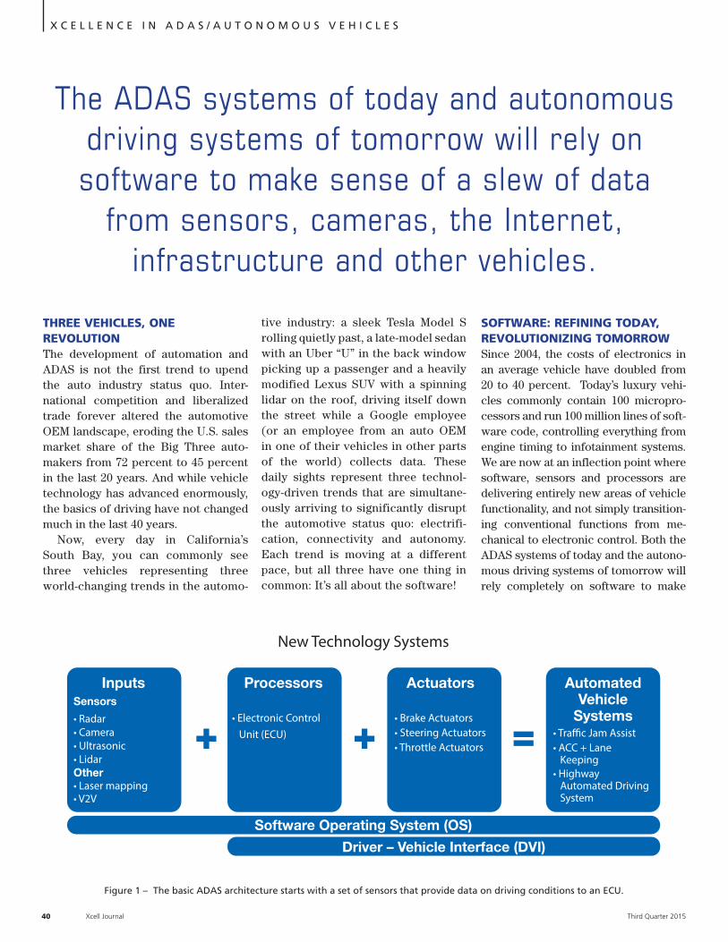
X C E L L E N C E I N A D A S / A U T O N O M O U S V E H I C L E S
40 Xcell Journal Third Quarter 2015
THREE VEHICLES, ONE REVOLUTION The development of automation and ADAS is not the first trend to upend the auto industry status quo. Inter-national competition and liberalized trade forever altered the automotive OEM landscape, eroding the U.S. sales market share of the Big Three auto-makers from 72 percent to 45 percent in the last 20 years. And while vehicle technology has advanced enormously, the basics of driving have not changed much in the last 40 years.
Now, every day in California’s South Bay, you can commonly see three vehicles representing three world-changing trends in the automo-
SOFTWARE: REFINING TODAY, REVOLUTIONIZING TOMORROW Since 2004, the costs of electronics in an average vehicle have doubled from 20 to 40 percent. Today’s luxury vehi-cles commonly contain 100 micropro-cessors and run 100 million lines of soft-ware code, controlling everything from engine timing to infotainment systems. We are now at an inflection point where software, sensors and processors are delivering entirely new areas of vehicle functionality, and not simply transition-ing conventional functions from me-chanical to electronic control. Both the ADAS systems of today and the autono-mous driving systems of tomorrow will rely completely on software to make
tive industry: a sleek Tesla Model S rolling quietly past, a late-model sedan with an Uber “U” in the back window picking up a passenger and a heavily modified Lexus SUV with a spinning lidar on the roof, driving itself down the street while a Google employee (or an employee from an auto OEM in one of their vehicles in other parts of the world) collects data. These daily sights represent three technol-ogy-driven trends that are simultane-ously arriving to significantly disrupt the automotive status quo: electrifi-cation, connectivity and autonomy. Each trend is moving at a different pace, but all three have one thing in common: It’s all about the software!
The ADAS systems of today and autonomous driving systems of tomorrow will rely on software to make sense of a slew of data
from sensors, cameras, the Internet, infrastructure and other vehicles.
InputsSensors
• Radar• Camera• Ultrasonic• LidarOther• Laser mapping• V2V
Processors
• Electronic ControlUnit (ECU)
Actuators
• Brake Actuators• Steering Actuators• Throttle Actuators
AutomatedVehicle
Systems• Tra�c Jam Assist• ACC + Lane
Keeping• Highway
Automated DrivingSystem
Software Operating System (OS)
Driver – Vehicle Interface (DVI)
New Technology Systems
Figure 1 – The basic ADAS architecture starts with a set of sensors that provide data on driving conditions to an ECU.

X C E L L E N C E I N A D A S / A U T O N O M O U S V E H I C L E S
Third Quarter 2015 Xcell Journal 41
sense of a slew of data from sensors, cameras, the Internet, infrastructure and other vehicles. The increasing complexity of vehi-cles has already shifted the automotive value chain. The trends of electrifica-tion, connectivity and automation will only accelerate this shift in value to-ward those companies that create elec-tronics and software, and away from OEMs that fail to innovate.
This shift will have two effects. First, software will become a critical mar-ket differentiator, pressuring OEMs to shorten product cycles and provide support and updates for legacy systems. To meet consumer demands for current technology, OEMs are now forced to significantly modify or introduce new models after only three or four years, while previous product cycles averaged five to eight years. This leaves OEMs with many challenges including rapid innovation, complex QA testing, higher development costs, less time to amor-tize R&D and the need for new sales and vehicle-ownership models.
Second, the shift to software allows new entrants to innovate in an industry with notoriously high barriers to en-try. After decades of the same players dominating the industry, Google, Apple, Tesla and Uber are all poised to remake the automotive landscape through soft-ware, a thought that would have seemed highly unlikely even five years ago.
In a typical ADAS-equipped vehicle (Figure 1), applications such as forward collision avoidance (FCA) are enabled by a set of sensors that provide data on the external driving environment to an electronic control unit (ECU). This unit then uses software to determine wheth-er a threat is present and operates brake actuators (or potentially, other counter-measures) to mitigate the threat.
The sensors available today for driver assistance applications are the hardware foundation for autonomous vehicles. But tomorrow’s sensors will necessarily be smaller, faster and cheaper. For example, Continental AG’s sensors and processors can transmit
Driving Environment Complexity
Threat Complexity
Sp
eed
HighLow
Fas
tS
low
InterstateCrusing
Parking
FreewayMergingOn/Off
StateHighway
ResidentialStreets &
IntersectionsCity Streets
&Intersections
HighwayTraffic Jam
Figure 2 – ADAS software algorithms must account for road types, speed and threat complexity.
Technology Introduction Paths
Complexity of Environment
HighLow
High
Low
TechnologyFunctionality
Figure 3 – Simpler systems like “traffic jam assist” will roll out first, followed by systems able to operate the vehicle.

X C E L L E N C E I N A D A S / A U T O N O M O U S V E H I C L E S
42 Xcell Journal Third Quarter 2015
and recalculate algorithms needed to understand the driving environment every 10 to 60 milliseconds, while the human brain can pass a message from a sensory neuron to a motor neuron in only a few milliseconds.
But the real gap between the ADAS systems of today and the fully autono-mous systems of tomorrow is seen in software. Regardless of how fast inputs can be processed, the software algo-rithms that will allow vehicles to drive themselves more efficiently and safely than human drivers in complex driving environments remain the biggest chal-lenge. Complexity is defined by both the number of threats, characterized by the types of threats that a driver can en-counter on different road types (for ex-ample, pedestrians, vehicles traveling at a right angle to your vehicle, bicyclists) and the speed at which the vehicle is driving (see Figure 2).
As they race to improve their soft-ware, vehicle OEMs and their suppliers are introducing their technology to the market in three distinct ways. OEMs such as BMW, Daimler and Nissan have already begun to sell moderate-func-tionality ADAS systems designed to operate in simple driving environments such as interstates. Without needing to account for traffic signals, turns or multidirectional traffic, these vehicles automatically steer, brake and accel-erate in lower-speed situations using systems like “traffic jam assist” (a tra-jectory represented by the blue line in Figure 3). Eventually, systems will op-erate at higher speeds or in more-com-
plex urban settings, and offer addition-al functionality such as the ability to merge, change lanes or negotiate an intersection. A subset of these OEMs, such as Volvo and Ford, are introduc-ing moderate-functioning systems for defined geographic areas (typically geo-fenced), such as a particular stretch of an interstate between two cities, to take advantage of laser scan mapping data. Over time, system functionality will in-crease and the number and complexity of geographic areas available to the sys-tem will expand (green line in Figure 3). Finally, Google’s approach has been to develop a highly functioning, fully au-tonomous vehicle from the outset (in geo-fenced areas and for low-speed city or campus driving), then test and refine its capabilities in increasingly complex environments (in orange on Figure 3).
CONSUMER ADOPTION AND DIFFUSION While OEMs are choosing different strategies to bring ADAS and vehicle autonomy to market, ADAS-equipped vehicles of increasing capability have already been introduced nearly every year since 2010 and continue to roll out annually. In 2013, fully 29 percent of pas-senger vehicle models offered optional forward-collision warning, and of those, 12 percent had autonomous braking. This year’s Mercedes entry-level premi-um CLA sedans come standard with a forward-collision prevention system, and Volvo has made its City Safety brak-ing system standard on its XC60 since 2010. Now that the early generations of
this technology are available, how fast will consumers adopt it?
To understand the adoption of ADAS-enabled and autonomous vehi-cles, it is instructive to look at adoption rates of other technologies. As a general trend, modern technologies such as the cell phone, Internet and PC have been adopted at a much faster rate than old-er technologies such as the VCR or TV. Cars have conventionally been one of the slower technologies to be adopted. This is largely due to their high relative cost as compared with consumer elec-tronics, and to the need for highways to be constructed. In contrast, the smart-phone is considered to be the fastest- adopted technology in history, on track to reach saturation in a decade. Mobile phones (largely what we today call “fea-ture phones”) took 20 years to reach sat-uration and conventional landlines took a century (largely because of the need to build out the landline networks).
ADAS-equipped and autonomous vehicles likely will be adopted at rates slightly slower than other modern tech-nology due to vehicle costs, but they will still be adopted much faster than conventional automobiles were. As with the uptake of other new technol-ogies, we expect a wave of first movers and early adopters to drive early sales of ADAS-equipped vehicles, followed by gradual adoption by the majority of consumers once the safety benefits have been proven (see Figure 4). Impor-tantly, the current additional cost of a typical ADAS suite of equipment is only about $3,000 (declining at about 7 to 9
The software algorithms that will let vehicles drive themselves more efficiently and safely than human drivers in complex environments
remain the biggest challenge.
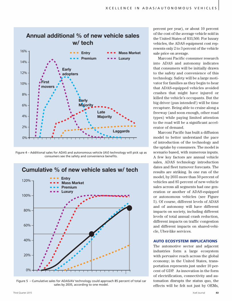
Third Quarter 2015 Xcell Journal 43
X C E L L E N C E I N A D A S / A U T O N O M O U S V E H I C L E S
percent per year), or about 10 percent of the cost of the average vehicle sold in the United States of $33,560. For luxury vehicles, the ADAS equipment cost rep-resents only 2 to 3 percent of the vehicle sale price on average.
Marconi Pacific consumer research into ADAS and autonomy indicates that consumers will be initially drawn to the safety and convenience of this technology. Safety will be a large moti-vator for families as they begin to hear that ADAS-equipped vehicles avoided crashes that might have injured or killed the vehicle’s occupants. But the big driver (pun intended!) will be time recapture. Being able to cruise along a freeway (and soon enough, other road types) while paying limited attention to the road will be a significant accel-erator of demand.
Marconi Pacific has built a diffusion model to better understand the pace of introduction of the technology and the uptake by consumers. The model is scenario based, with numerous inputs. A few key factors are annual vehicle sales, ADAS technology introduction dates and fleet turnover forecasts. The results are striking. In one run of the model, by 2035 more than 50 percent of vehicles and 85 percent of new-vehicle sales across all segments had one gen-eration or another of ADAS-equipped or autonomous vehicles (see Figure 5). Of course, different levels of ADAS and of autonomy will have different impacts on society, including different levels of total annual crash reduction, different impacts on traffic congestion and different impacts on shared-vehi-cle, Uber-like services.
AUTO ECOSYSTEM IMPLICATIONS The automotive sector and adjacent industries form a large ecosystem with pervasive reach across the global economy; in the United States, trans-portation represents just under 10 per-cent of GDP. As innovation in the form of electrification, connectivity and au-tomation disrupts the status quo, the effects will be felt not just by OEMs,
Annual additional % of new vehicle salesw/ tech
Laggards
16% –
14% –
12% –
10% –
8% –
6% –
4% –
2% –
0%
Firstmovers
Earlyadopters
LateMajority
Entry
Premium
Mass Market
Luxury
– – – – – – – – – – – – – – – – – – – – – – – – –
EarlyMajority
Figure 4 – Additional sales for ADAS and autonomous vehicle (AV) technology will pick up as consumers see the safety and convenience benefits.
Cumulative % of new vehicle sales w/ tech
120% –
100% –
80% –
60% –
40% –
20% –
0%
Entry
PremiumMass Market
Luxury
– – – – – – – – – – – – – – – – – – – – – –– –
Figure 5 – Cumulative sales for ADAS/AV technology could approach 85 percent of total car sales by 2035, according to one model.

X C E L L E N C E I N A D A S / A U T O N O M O U S V E H I C L E S
44 Xcell Journal Third Quarter 2015
Xilinx All Programmable Devices:
De Facto Standard Platforms for ADAS and Beyond by Mike Santarini Publisher, Xcell JournalXilinx, Inc. [email protected]
Xilinx Inc. has a rich his-tory in the automotive market, but over the last four years and with the commercial launch of the Zynq®-7000 All
Programmable SoC in 2011, the com-pany has quickly become the platform provider of choice in the burgeoning market for advanced driver assistance systems (ADAS). Companies such as Mercedes-Benz, BMW, Nissan, VW, Hon-da, Ford, Chrysler, Toyota, Mazda, Acu-ra, Subaru and Audi are among the many OEMs that have placed Xilinx® FPGAs and Zynq SoCs at the heart of their most advanced ADAS systems. And with the new Zynq UltraScale+™ SoCs, Xilinx is sure to play a leadership role in the next phases of automotive electronic innova-tion: autonomous driving, vehicle-to-ve-hicle communication and vehicle-to-in-frastructure communication.
The basic goal of an ADAS technology is to make drivers more aware of their en-vironment so they can drive safely while enjoying the driving experience. Around 10 years ago, luxury OEMs began to of-fer the first ADAS systems in the form of backup radar/lidar sensor-based products that would simply beep if they detected an object behind the vehicle. Over time, these systems advanced to multisensor versions that fused radar with cameras and even lidar, to not only give drivers a view of what’s behind them but also detect if something is coming up from the side.
In subsequent years, the ADAS sen-sor arrays morphed from doing one task at the back of a vehicle into networked sensor arrays that see 360 degrees around and even inside an automobile, with each
sensor performing a number of tasks. To-day’s high-end automobiles can include ADAS products with not only highly advanced rear-camera systems, but fu-sion-sensor systems that simultaneously perform multiple tasks such as blind-spot and lane-departure warning, pedestri-an and sign detection, automated cruise control, forward-collision warning and even drowsy-driver detection and warn-ing. The latter system monitors the driv-er’s eyes to detect eye patterns that may indicate he or she is falling asleep at the wheel and needs a sonic alert or even a puff of smelling salts to snap to.
What’s more, over the last five years, an increasing number of features once offered only in premium vehicle lines are quickly becoming standard in even econ-omy lines. In short, OEMs are leveraging ADAS as competitive selling points for their vehicles.
Today, OEMs are moving above and be-yond the ADAS warning features and are starting to network ADAS into the con-trols of the vehicle to actively and momen-tarily take charge. Adaptive cruise control, intelligent speed control, lane-keep assist, collision avoidance and even automated parking are available in many models. And these remarkable technologies represent the first steps in the automotive industry’s race to offer consumers fully autonomous, self-driving vehicles in which the driver is essentially the copilot. What’s more, these technologies will also be leveraged heav-ily to facilitate vehicle-to-vehicle and ve-hicle-to-infrastructure (V2X) communica-tions designed to enable governments to build smart infrastructure—streets, traffic signals and so on—to streamline traffic flow in real time, making transportation safer, more efficient and economical, and better for the environment.
Xilinx’s All Programmable devices and especially the multi-award-winning Zynq SoC are at the heart of today’s most so-
phisticated ADAS systems and are quick-ly replacing much less versatile ASSPs. The combination of the Zynq SoC’s ARM® processors and FPGA logic on the same device has enabled OEMs to build highly sophisticated, All Programmable ADAS platforms that can scale with automotive product lines and be upgraded with new enhancements to suit demanding and ever-evolving customer requirements.
Automotive OEMs leverage the Zynq SoC in many platform configurations. The device serves as a multisensor, multifea-ture driver assist platform, a high-resolu-tion video and graphics platform, a vehi-cle networking and connectivity platform, and an image-processing and recognition platform. In these applications, customers implement algorithms for their design’s most complex and compute-intensive functions in the logic portion of the Zynq SoC and implement serial processing functions in the onboard ARM process-ing system. They leverage the Zynq SoC’s high-speed I/O to link to sensors and cre-ate highly reliable connections to automo-tive networks. Customers also leverage IP from Xilinx and from members of the Xilinx Alliance Program, as well as Xil-inx’s Vivado® Design Suite and the new SDSoC™ development environments, to quickly develop ADAS platforms.
Xilinx’s new Zynq Ultrascale+ SoC is destined to enable these same OEMs to bring autonomous vehicles to the mass market. With 64-bit application proces-sors, real-time processors, on-chip memo-ry and FPGA logic on the same device, the UltraScale+ version of the Zynq SoC will allow OEMs to create ever-more-sophisti-cated fusion systems with a programma-ble platform that can’t be matched by any other silicon architecture.
For more information on Xilinx’s role in the rapidly advancing ADAS market, visit http://www.xilinx.com/applications/
automotive.html.
Third Quarter 2015 Xcell Journal 45
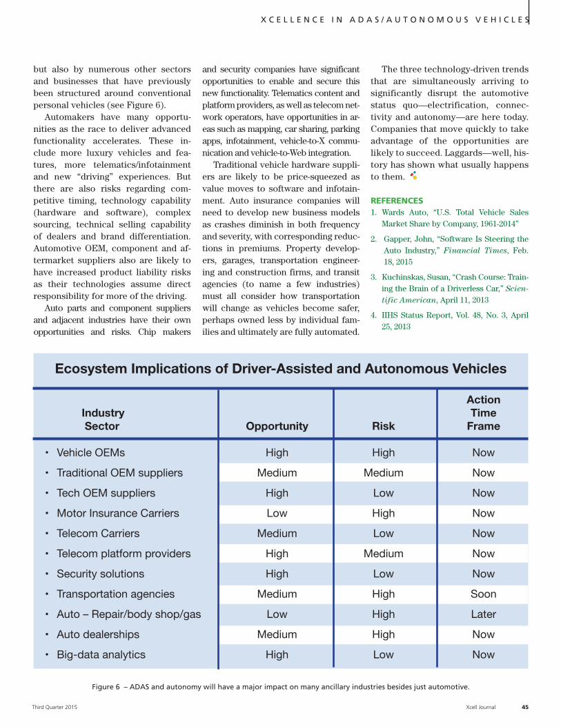
X C E L L E N C E I N A D A S / A U T O N O M O U S V E H I C L E S
but also by numerous other sectors and businesses that have previously been structured around conventional personal vehicles (see Figure 6).
Automakers have many opportu-nities as the race to deliver advanced functionality accelerates. These in-clude more luxury vehicles and fea-tures, more telematics/infotainment and new “driving” experiences. But there are also risks regarding com-petitive timing, technology capability (hardware and software), complex sourcing, technical selling capability of dealers and brand differentiation. Automotive OEM, component and af-termarket suppliers also are likely to have increased product liability risks as their technologies assume direct responsibility for more of the driving.
Auto parts and component suppliers and adjacent industries have their own opportunities and risks. Chip makers
and security companies have significant opportunities to enable and secure this new functionality. Telematics content and platform providers, as well as telecom net-work operators, have opportunities in ar-eas such as mapping, car sharing, parking apps, infotainment, vehicle-to-X commu-nication and vehicle-to-Web integration.
Traditional vehicle hardware suppli-ers are likely to be price-squeezed as value moves to software and infotain-ment. Auto insurance companies will need to develop new business models as crashes diminish in both frequency and severity, with corresponding reduc-tions in premiums. Property develop-ers, garages, transportation engineer-ing and construction firms, and transit agencies (to name a few industries) must all consider how transportation will change as vehicles become safer, perhaps owned less by individual fam-ilies and ultimately are fully automated.
The three technology-driven trends that are simultaneously arriving to significantly disrupt the automotive status quo—electrification, connec-tivity and autonomy—are here today. Companies that move quickly to take advantage of the opportunities are likely to succeed. Laggards—well, his-tory has shown what usually happens to them.
REFERENCES 1. Wards Auto, “U.S. Total Vehicle Sales
Market Share by Company, 1961-2014”
2. Gapper, John, “Software Is Steering theAuto Industry,” Financial Times, Feb.18, 2015
3. Kuchinskas, Susan, “Crash Course: Train-ing the Brain of a Driverless Car,” Scien-tific American, April 11, 2013
4. IIHS Status Report, Vol. 48, No. 3, April25, 2013
Figure 6 – ADAS and autonomy will have a major impact on many ancillary industries besides just automotive.
Ecosystem Implications of Driver-Assisted and Autonomous Vehicles
Action Industry Time
Sector Opportunity Risk Frame
• VehicleOEMs High High Now
• TraditionalOEMsuppliers Medium Medium Now
• TechOEMsuppliers High Low Now
• MotorInsuranceCarriers Low High Now
• TelecomCarriers Medium Low Now
• Telecomplatformproviders High Medium Now
• Securitysolutions High Low Now
• Transportationagencies Medium High Soon
• Auto–Repair/bodyshop/gas Low High Later
• Autodealerships Medium High Now
• Big-dataanalytics High Low Now
Third Quarter 2015 Xcell Journal 45

X C E L L E N C E I N D AT A C E N T E R C L O U D C O M P U T I N G
46 Xcell Journal Third Quarter 2015
Machine Learning in the Cloud: Deep Neural Networks on FPGAs by Nagesh Gupta Founder and CEOAuviz Systems [email protected]

X C E L L E N C E I N D A T A C E N T E R C L O U D C O M P U T I N G
Third Quarter 2015 Xcell Journal 47
Artificial intelligence is undergoing a revolution thanks to the rapid advances in machine learning. Within the field of machine learning, a class of al-gorithms called “deep learning” is generating a lot of interest because of its excellent performance in large data sets. In deep learning, the machine can learn a task from a large amount of data in either a supervised or an unsupervised manner. Large-scale supervised learning has been very successful in tasks such as image recognition and speech recognition.
Deep-learning techniques use a large amount of known data to find a set of weights and bias val-ues to match the expected results. The process is called training, and it can result in large models. This fact has motivated engineers to move toward specialized hardware such as GPUs for training and classification purposes.
As the amount of data increases even further, machine learning will move to the cloud, where large machine-learning models would be imple-mented on CPUs. While GPUs are a better alter-native in terms of performance for deep-learning algorithms, the prohibitive power requirements have limited their use to high-performance com-puting clusters. Therefore, there is a dire need for a processing platform that can accelerate algorithms without a substantial increase in power consump-tion. In this context, FPGAs seem to be an ideal choice, with their inherent capability to facilitate the launching of a large number of concurrent pro-cesses at a low power profile.
Let’s take a closer look at how to implement a convolutional neural network (CNN) on a Xil-inx® FPGA. CNN is a class of deep neural net-works that has been very successful for large-scale image-recognition tasks and other, similar machine-learning problems. In the current sce-nario, a feasibility study of implementing CNN on
Because of their attractive performance/power metrics, Xilinx FPGAs are a top choice for designers building convolutional neural networks. New software tools ease the implementation job.
A

X C E L L E N C E I N D A T A C E N T E R C L O U D C O M P U T I N G
48 Xcell Journal Third Quarter 2015
FPGAs can serve as an indicator as to whether FPGAs are fit for large-scale machine-learning problems.
WHAT IS A CONVOLUTIONAL NEURAL NETWORK? Convolutional neural networks are a form of deep neural networks (DNNs) that engineers have recently begun us-ing for various recognition tasks. Image recognition, speech recognition and natural-language processing are a few popular applications of the CNNs.
In 2012, Alex Krishevsky and oth-ers [1] from the University of Toronto proposed a deep architecture based on CNNs that won that year’s Imagenet Large Scale Visual Recognition Chal-lenge. Their model achieved a sub-stantial improvement in recognition compared with its competitors or with models from previous years. Since then, AlexNet has become the bench-mark for comparison in all image-rec-ognition tasks.
AlexNet consists of five convolu-tion layers followed by three dense
convolution operation from pixel loca-tion (x,y) at the input feature map n.
The activation function used is a rectified linear unit, which performs the function Max(x,0). The activation function introduces nonlinearity in the transfer function of the network. Max pooling is the subsampling technique used in AlexNet. Using this technique, only the maximum values in the local neighborhood of a pixel are selected to propagate to the next layer.
DEFINING DENSE LAYERS A dense layer in AlexNet corresponds to a fully connected layer, wherein every in-
put node is connected to each of the out-put nodes. The first dense layer in Alex-Net has 9,216 input nodes. This vector is multiplied with a weight matrix to create output in 4,096 output nodes. In the next
layers (Figure 1). Each convolution layer convolves the set of input feature maps with a set of weight filters, re-sulting in a set of output feature maps. The dense layers are fully connected layers, where every output is a func-tion of all the inputs.
CONVOLUTION LAYER A convolution layer in AlexNet does three major jobs, as shown in Figure 2: 3D convolutions, activation function using a rectified linear unit (ReLu) and subsampling (max pooling). Three-di-mensional convolutions are represent-ed by the following equation:
where Y(m,x,y) is the output of convo-lution at location (x,y) for output fea-ture map m, S is the local neighborhood around (x,y), W is the set of convolution filters and X(n,x,y) is the input to the
Image recognition, speech recognition and natural-language processing are a few popular
applications of the CNNs.
dense densedense
Maxpooling 4096 4096
1000
Maxpooling
Maxpooling
Strideof 4
InputImage(RGB)
Figure 1 – AlexNet, an image-recognition benchmark, consists of five convolution layers (blue boxes) and three dense layers (yellow).
Y (m, x, y) = ∑ ∑ W (m, n, ∆x, ∆y)X(n, x – ∆x, y – ∆y)n=1 (∆x,∆y) S
N
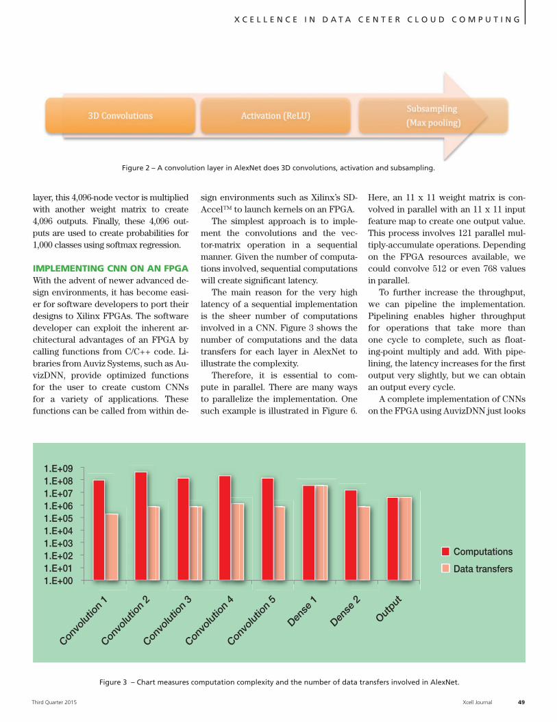
X C E L L E N C E I N D A T A C E N T E R C L O U D C O M P U T I N G
Third Quarter 2015 Xcell Journal 49
layer, this 4,096-node vector is multiplied with another weight matrix to create 4,096 outputs. Finally, these 4,096 out-puts are used to create probabilities for 1,000 classes using softmax regression.
IMPLEMENTING CNN ON AN FPGA With the advent of newer advanced de-sign environments, it has become easi-er for software developers to port their designs to Xilinx FPGAs. The software developer can exploit the inherent ar-chitectural advantages of an FPGA by calling functions from C/C++ code. Li-braries from Auviz Systems, such as Au-vizDNN, provide optimized functions for the user to create custom CNNs for a variety of applications. These functions can be called from within de-
sign environments such as Xilinx’s SD- Accel™ to launch kernels on an FPGA.
The simplest approach is to imple-ment the convolutions and the vec-tor-matrix operation in a sequential manner. Given the number of computa-tions involved, sequential computations will create significant latency.
The main reason for the very high latency of a sequential implementation is the sheer number of computations involved in a CNN. Figure 3 shows the number of computations and the data transfers for each layer in AlexNet to illustrate the complexity.
Therefore, it is essential to com-pute in parallel. There are many ways to parallelize the implementation. One such example is illustrated in Figure 6.
Here, an 11 x 11 weight matrix is con-volved in parallel with an 11 x 11 input feature map to create one output value. This process involves 121 parallel mul-tiply-accumulate operations. Depending on the FPGA resources available, we could convolve 512 or even 768 values in parallel.
To further increase the throughput, we can pipeline the implementation. Pipelining enables higher throughput for operations that take more than one cycle to complete, such as float-ing-point multiply and add. With pipe-lining, the latency increases for the first output very slightly, but we can obtain an output every cycle.
A complete implementation of CNNs on the FPGA using AuvizDNN just looks
Figure 2 – A convolution layer in AlexNet does 3D convolutions, activation and subsampling.
1.E+091.E+081.E+071.E+061.E+051.E+041.E+031.E+021.E+011.E+00
Computations
Convo
lutio
n 1
Convo
lutio
n 2
Convo
lutio
n 3
Convo
lutio
n 4
Convo
lutio
n 5
Dense
1
Dense
2
Output
Data transfers
Figure 3 – Chart measures computation complexity and the number of data transfers involved in AlexNet.

X C E L L E N C E I N D A T A C E N T E R C L O U D C O M P U T I N G
50 Xcell Journal Third Quarter 2015
like a sequence of function calls from a C/C++ program. After setting up the ob-jects and data containers, function calls are made to create each of the convo-lution layers, followed by the dense layers and finally the softmax layer, as shown in Figure 4.
AuvizDNN, a library of functions to implement CNNs on FPGAs from Au-viz Systems, provides all the required objects, classes and functions to imple-ment CNNs easily. The users just need to supply the required parameters to create different layers. For example, the code snippet in Figure 5 shows how the
first layer in AlexNet can be created. AuvizDNN provides configurable
functions with which you can create any type and configuration of CNN. AlexNet is used just as an illustration. The CNN implementation is loaded into the FPGA as a complete bitstream and called from the C/C++ program, allowing develop-ers to use AuvizDNN without running the implementation software.
FPGAs have a large number of lookup tables (LUTs), DSP blocks and on-chip memory, which make them a good choice to implement very deep CNNs. More im-portant than raw performance in the con-
text of data centers is performance per watt. Data centers require high perfor-mance but at a power profile within the limits of data center server requirements.
FPGAs, such as Xilinx’s Kintex® Ul-traScale™ devices, can provide higher than 14 images per second per watt, making it a great choice for data cen-ter applications. Figure 6 will give you an idea of the achievable performance with different classes of FPGAs.
IT ALL STARTS WITH C/C++ Convolutional neural networks are becoming increasingly popular and are being deployed at a large scale for tasks such as image recognition, natural speech processing and many others. As CNNs migrate from high-performance computing applications (HPC) to the data center, efficient methods are re-quired to implement them.
FPGAs can be used to implement CNNs very efficiently. FPGAs also pro-vide a very good performance/watt met-ric, and so are suitable for the data center.
AuvizDNN provides a library of func-tions to implement CNNs on FPGAs. AuvizDNN masks the complexity of us-
Figure 5 – Code snippet for creating Layer 1 of AlexNet using AuvizDNN.
/*********** calling convolution layer functions***********/
OclConv.loadkernel(convolutionLayer_xclbin);
// Layer 1poolDesc.createPoolingDesc(pool_mode,window_size,pool_stride);
tensorØ.createTensor(datatype,b,3,224,224);
tensor1.createTensor(datatype,b,96,55,55);
conv_filter1.createConvFilter(datatype,96,3,11,11):tensorØ.moveTensorData(contex, input_data, HOST2DEVICE);conv_filter1.moveConvFilter(context, con1_data, HOST2DEVICE);bias1.createBiasVector(datatype, 96);bias1.moveBiasVector(context, bias1_data, HOST2DEVICE);poolDesc.movePoolingDesc(context, HOST2DEVICE);clFinish();OclConv.convolutionForward(tensorØ,con_filter1,tensor1,bias1,NULL,RELU, 4);
Figure 4 — Here is the sequence of function calls to implement a CNN.

Third Quarter 2015 Xcell Journal 51
X C E L L E N C E I N D A T A C E N T E R C L O U D C O M P U T I N G
ing an FPGA, and provides simple func-tions that users can call from their C/C++ program to get the acceleration on the FPGA. With AuvizDNN, getting the acceleration of FPGAs is not any dif-
ferent than writing C/C++ with calls to functions within the AuvizDNN library.
For further information, visit www.auvizsystems.com or e-mail [email protected].
REFERENCE 1. A. Krizhevsky, I. Sutskever, G. E. Hinton, “ImageNet Classification with Deep Convolu-tional Neural Networks,” Advances in Neural Information Processing Systems, 2012
Figure 6 – Performance of AlexNets will vary depending on the class of FPGA chosen.
300
250
200
150
100
50
0167 200 250 300 167 200 250 300 167 200 250 300
256 Multiply & Adds
512 Multiply & Adds
768 Multiply & Adds
Frequency of operation, MHz
Imag
es/se
c
Xilinx Kintex Ultrascale XCKU115 class FPGAs
Xilinx Virtex 7 XC7VX690T class FPGAs
200 Gbps bandwidthVITA 57 compliant
www.techway.eu
The highest optical
bandwidth for FPGA
carrier
TigerFMC
X C E L L E N C E I N S D N / N F V
52 Xcell Journal Third Quarter 2015
All Programmable SDN Switch Speeds Network Function Virtualization
A programmable COTS NIC based on a Xilinx FPGA accelerates the performance of NFV software applications by 50x.
by David Levi Chief Executive OfficerEthernity Networks [email protected]
X C E L L E N C E I N S D N / N F V
Third Quarter 2015 Xcell Journal 53
The shift toward network function vir-tualization (NFV) and software-defined networks (SDN) represents the most transformative architectural network trend in nearly 20 years. With their promise of open systems and network neutrality, NFV and SDN stand poised to make a far-reaching impact in shap-ing the communications networks and businesses of tomorrow.
We at Ethernity Networks are lever-aging Xilinx® devices to bring truly open and highly programmable SDN and NFV solutions to the market sooner. Let’s take a look at how Ethernity crafted its solution, after first exploring the prom-ise and requirements of NFV and SDN.
UBIQUITOUS HARDWARE AND THE NFV/SDN REVOLUTION The network infrastructure business of the last few decades has largely been a continuance of the mainframe business model in which a handful of large cor-porations offer proprietary infrastruc-ture equipment that runs proprietary software, all purposefully built not to communicate with systems from com-petitors. In most cases, infrastructure vendors create custom hardware for each node of their customer’s network, and they build each node to be mini-mally programmable and upgradable, ensuring that customers wanting to ex-pand or upgrade their networks would need to buy next-generation equipment from the same vendor or make the futile choice of buying an entirely new net-work from another company but run-ning into the same consequences.
need to be reprogrammable to optimize overall system performance. This allows vendors and operators to leverage NFV and SDN in a “work smarter, not hard-er” manner to meet growing network demands of the operators’ end custom-ers—consumers. A truly hardware- and software-programmable infrastructure is the only way to truly realize the vision of NFV and SDN.
SDN is a modern approach to net-working that eliminates the complex and static nature of legacy distribut-ed network architectures through the use of a standards-based software ab-straction between the network control plane and underlying data-forward-ing plane in both physical and virtu-al devices. Over the last five years, the industry has developed a stan-dards-based data plane abstraction called OpenFlow that provides a novel and practical approach to dynamically provisioning the network fabric from a centralized software-based controller.
An open SDN platform with cen-tralized software provisioning delivers dramatic improvements in the network agility via programmability and auto-mation, while substantially reducing the cost of the network operations. An industry-standard data plane abstrac-tion protocol like OpenFlow gives providers the freedom to use any type and brand of data plane device, since all the underlying network hardware is addressable through a common ab-straction protocol. Importantly, Open-Flow facilitates the use of “bare-metal switches” and eliminates traditional vendor lock-in, giving operators the same freedom of choice in networking as can be found today in other areas of IT infrastructure, such as servers.
Because SDN is in its infancy, stan-dards are still in flux. This means that equipment vendors and operators need to hedge their bets and design and operate SDN equipment with maximum flexibility, leveraging the hardware and software programma-bility of FPGAs. FPGA-based SDN equipment entering the market today
In the last five years, operators, academics and vendor upstarts have been calling for a move to ubiquitous hardware, network neutrality, open systems and software compatibility by maximizing hardware and software programmability. NFV and SDN are at the vanguard of this trend, carrying the banner for this growing and sure-to-succeed revolution.
With NFV, companies run a variety of network functions in software on commodity, general-purpose hardware platforms, as opposed to running each specialized network task on custom-ized and expensive proprietary hard-ware. Maximizing programmability on these open, ubiquitous platforms en-ables companies to run in data centers, or even in smaller networked nodes, many tasks heretofore performed by specialized hardware devices. NFV fur-ther aims to reduce the time it takes to establish a new network service by al-lowing operators to simply upload new network software of a given service to the commodity hardware resources as needed. This allows operators to scale networks easily and choose best-in-class functionality for their businesses instead of being forced to purchase and operate new proprietary hardware that affords limited software flexibility.
NFV can be effective because many nodes in a network share common func-tionality requirements. Those nodes with common requirements include switching and routing, classification of millions of flows, access control lists (ACL), stateful flow awareness, deep packet inspection (DPI), tunneling gateway, traffic analysis, performance monitoring, fragmentation, security, vir-tual routing and switching. NFV has its challenges, however. With exponential growth expected in Internet and data center traffic in the coming years, net-work infrastructure equipment must be able to handle vast increases in traffic. Software programmability alone won’t be enough to enable generic hardware to scale easily with growing bandwidth demands. The ubiquitous hardware will
T

X C E L L E N C E I N S D N / N F V
54 Xcell Journal Third Quarter 2015
is quite affordable even for mass de-ployment. It offers the highest degree of hardware and software flexibili-ty and maximizes compliance with OpenFlow.
THE NEED FOR PERFORMANCE ACCELERATION Perhaps the most critical requirement for both NFV and SDN above and be-yond openness is high performance. While NFV hardware will seemingly be less expensive than proprietary systems, NFV architectures will need to sustain competitively high data volumes, meet complex processing requirements for next-generation networking and be in-creasingly energy efficient.
In fact, the NFV Infrastructure Group Specification includes a spe-cial section describing the need for
(VM) based on tag information such as IP, MAC or VLAN. The packet is then DMA’ed directly to the right VM locat-ed at the server for processing. Each virtual networking function (VNF) runs on a different VM, and certain networking functions require the use of multiple or even tens of VMs.
OpenFlow controls the hardware acceleration functions, such that these hardware acceleration functions locat-ed at the NIC can be viewed as an ex-tension of the SDN switch.
NFV performance can be addressed for many functions by deploying multi-ple VNFs on multiple VMs and/or cores. This raises two main performance chal-lenges for NFV. The first challenge is at the “vSwitch,” which is typically a piece of software that processes net-work traffic between the Ethernet NIC and the virtual machines. The second performance challenge is balancing in-coming 40/100GE data among multiple VMs. When adding IP fragmentation, TCP segmentation, encryption or oth-er dedicated hardware functions, NFV software requires assistance to meet the performance needs and reduce the power. Ideally, it should be compact to reduce the amount of real estate re-quired to house the network equipment.
To address NFV challenges and the variety of networking functions, NIC cards for NFV and SDN must be ex-tremely high performance but also as flexible as possible.
In an attempt to be first to market with NFV hardware, several chip ven-dors have proposed platforms for NIC cards, each with some degree of pro-grammability. Intel today is the main NIC component provider, equipped with its DPDK package for packet-process-ing acceleration. EZchip offers its NPS multithreaded CPU running Linux and programmed in C. Marvell offers two all-inclusive data plane software suites for its Xelerated processor for both metro Ethernet and the Unified Fiber Access Application, which consist of an application package running on the NPU and a control-plane API running
acceleration to increase network per-formance. The specification describes how a processor component can off-load certain functions to a network interface card (NIC) to support cer-tain acceleration functions, including TCP segmentation, Internet Protocol (IP) fragmentation, DPI, filtering of millions of entries, encryption, perfor-mance monitoring/counting, protocol interworking and OAM, among other acceleration capabilities.
The main engine driving this accel-eration is the NIC, which is equipped with physical Ethernet interfaces to enable server connectivity to the net-work. As described in Figure 1, when a packet arrives the NIC, over 10GE, 40GE or 100GE ports, it is placed in a virtual port (VP) or queue that rep-resents a specific virtual machine
Figure 1 – When a packet arrives, the NIC enters a virtual port (VP) that represents a specific virtual machine. The packet is then sent through DMA
to the right virtual machine at the server for processing.
Virtual Machine Virtual Machine
Control Data
OpenFlow
Data in/outVNF
AccelerationPhysical NIC
VPVP VPn
Virtual Machine Virtual Machine
VNF1 VNFn
Server/CPU

X C E L L E N C E I N S D N / N F V
Third Quarter 2015 Xcell Journal 55
on a host CPU. Cavium has opted for a more generic software development kit for its Octeon family. Broadcom, Intel and Marvel L2/L3 switches are mainly used for search and vSwitch offload. Meanwhile, Netronome’s new Flow- NIC is equipped with software that runs on that company’s specialized network processor hardware.
While all of these offerings are claiming to be open NFV approaches, they really aren’t. All of the approaches involve rigid and, arguably, too restric-tive hardware implementations that are only programmable in software and rely once again on rigid, proprietary hardware implementations in SoCs or standard processors.
ALL PROGRAMMABLE ETHERNITY NIC FOR NFV PERFORMANCE ACCELERATION To add programmability while also improving performance dramatical-ly, many companies are examining a hybrid approach that pairs an off-the-shelf CPU with an FPGA. Over the last two years, a number of data center operators—most notably, Microsoft—
have published papers describing the dramatic performance increases they’ve gained with a hybrid architec-ture. In the case of Microsoft, a white paper titled “The Catapult Project” cites a 95 percent performance in-crease at a cost of only a 10 percent power increase. Intel cited the potency of this combination of FPGA-plus-CPU in data center NICs as the primary rea-son for its $16.7 billion acquisition of the No. 2 player in FPGAs, Altera Corp.
The same hybrid CPU-FPGA ap-proach is applicable for NFV, which runs virtual networking functions on virtual machines. In this approach, the FPGA serves as a complete programma-ble NIC that can be extended to accel-erate the virtual-network functions that run on the server’s CPUs/VMs.
But a NIC card based entirely on FPGAs is the ideal COTS hardware architecture for NFV. Multiple FPGA firmware vendors can provide firm-ware for NFV performance accelera-tion running on the FPGA NIC. And FPGA companies have recently de-veloped C compiler technologies such as Xilinx’s SDAccel™ and SDSoC™
development environments to enable OpenCL™ and C++ design entry and program acceleration, further open-ing up NFV equipment design to a greater number of users.
To accelerate NFV performance, NFV solution providers increase the number of VMs with a goal of distributing the VNFs on multiple VMs. When operating with multiple VMs, new challenges arise related to balancing the traffic load be-tween the virtual machines while sup-porting IP fragments. In addition, chal-lenges also exist in supporting switching between VMs and between VMs and the NIC. A pure software-based vSwitch el-ement simply doesn’t provide adequate performance to address these challeng-es. The integrity of the VMs must also be maintained so that the VMs store specif-ic bursts adequately and do not deliver packets out of order.
Focusing on solving the performance issues for NFV, Ethernity’s ENET FPGA firmware is equipped with a virtual switch/router implementation that en-ables a system to accelerate vSwitch functionality to switch data based on L2, L3 and L4 tags, while maintaining a dedicated virtual port for each VM. If a specific VM is not available, the ENET can store up to 100 milliseconds of traffic; then, upon availability, it will re-lease the data through DMA to the VM. Equipped with delay measurement ca-pabilities through an implementation of a standard CFM packet generator and a packet analyzer, our ENET can measure the availability and health of a VM and instruct the ENET’s stateful load balanc-er regarding the availability of each VM for load distribution. The packet reor-der engine can maintain the order of the frame if, for example, a packet moves out of order, which can result in the use of multiple VMs for one function.
Figure 2 depicts a block diagram of the the VM load-balancing ENET solution.
In Figure 2, the classification block performs hierarchical classification for L2, L3 and L4 fields to maintain a route for connection and flow supporting the long-lived TCP (telnet, FTP and more)
Network Server
HeaderManipulation
HierarchicalTraf�c Manager
Timing
CPU loadMonitoring
Sourceselection
ClassificationSearch
Onbound PacketInbound Packet
Destinationselection
Figure 2 – This high-level block diagram shows the virtual machine’s load balancing and switch.

X C E L L E N C E I N S D N / N F V
56 Xcell Journal Third Quarter 2015
selection block’s load balancer as-signs a destination address from the available VM according to the Weight-ed Round Robin (WRR) technique. The WRR is configured based on the information derived from the VM load-monitoring block.
The hierarchical traffic manager block implements hierarchical WRR between an available VM and maintains an output virtual port for each VM to include three scheduling hierarchies based on priority, VM and physical port. The CPU hierarchy represents a cer-tain VM, and the priority hierarchy may assign weights between different ser-vices/flows that are under the service of a specific VM. Operating with external DDR3, the ENET can support buffering of 100 ms to overcome the momentary load of a specific VM.
The VM load monitoring uses the ENET Programmable Packet Gener-ator and Packet Analyzer for carrier Ethernet service monitoring, which complies with Y.1731 and 802.1ag. The
VM load-monitoring block maintains information on the availability of each CPU/VM, using metrics such as Ethernet CFM Delay Measurements Message (DMM) protocol generation toward a VM. By time-stamping each sent packet and measuring the delta time between send and receive, the block can determine the availability of each VM and, based on that, in-struct the destination selection block on the available VMs.
The Source Selection block deter-mines what outbound traffic sent from the host to the user will be classified and determines the source of that packet.
The Header Manipulation block in ENET will perform network address translation (NAT) to replace the incom-ing address with the right VM IP address to enable the NIC to forward the flow, packet or service to the right VM. For outbound traffic, the NAT will perform the reverse action and will send out the packet to the user with its original IP address. The Header Manipulation
that doesn’t immediately close. The load balancer must ensure that mul-tiple data packets carried across that connection do not get load-balanced to other available service hosts. ENET includes an aging-mechanism feature to delete nonactive flows.
In the classification block, we con-figured the balancing hash algorithm based on L2, L3 and L4 fields. The algo-rithm includes fragmentation such that the load balancer is able to perform balancing based on inner tunnel infor-mation (such as VXLAN or NVGRE), while an IP fragment connection can be handled by a specific connection/CPU. For VM-to-VM connection, the classifier and search engine will for-ward the session to the destination VM instead of the vSwitch software. Meanwhile, a classifier feature assigns a header manipulation rule for each incoming flow based on its outgoing route, with eyes on modifying the IP address or offloading protocols.
For each new flow, the destination
12G/6.6GSERDES
12G/6.6GSERDES
12G/6.6GSERDES
12G/6.6GSERDES
12G/6.6GSERDES
12G/6.6GSERDES
12G/6.6GSERDES
12G/6.6GSERDES
DD
R 3
Co
ntro
ller
DD
R 3
Co
ntro
ller
DD
R 3
Co
ntro
ller
Xilinx’sKintex 325
DDR3
DDR3
DDR3
PCIe Gen 3 connector
10GEXFI
10GEXFI
10GEXFI
PCIE – GEN3
1. .4
1. .4
0. . .2
Search Tables
PacketMemory
PacketMemory
Figure 3 – A Xilinx Kintex FPGA is at the heart of Ethernity’s NFV network interface card.

Third Quarter 2015 Xcell Journal 57
X C E L L E N C E I N S D N / N F V
block also performs tunnel encapsu-lation. Here, the Header Manipulation block will execute the action rules as-signed by the classifier from the classifi-cation, and will strip out tunnel headers or other headers to or from the CPU op-eration. In the reverse direction, it will append the original tunnel toward the outgoing user port.
As the number of subscribers to an operator’s network increases, the size of the flow tables can quickly grow to exceed the cache capacity of standard servers. This is especially the case with current OpenFlow sys-tems, which have table entries that require 40 different fields, IPv6 ad-dresses, Multiprotocol Label Switch-ing (MPLS) and Provider Backbone Bridges (PBB). The ENET search en-gine and parser can support classifi-cation on multiple fields and serve millions of flows, thus offloading the classification and search function from the software appliance.
And finally, with the ENET packet header manipulation engine, the ENET can offload any protocol handling and provide raw data info to the VM togeth-er with TCP segmentation, or inter-working between various protocols, in-cluding 3GPP protocols for virtual EPC (vEPC) implementation, XVLAN, MPLS, PBB, NAT/PAT and so on.
In addition to the firmware, Etherni-ty has also developed an NFV NIC that we call the ACE-NIC (Figure 3). To cre-ate the NIC, we integrated our ENET SoC firmware (already deployed in hun-dreds of thousands of systems in carri-er Ethernet networks) into a single Xil-inx Kintex®-7 FPGA. We also integrated into the same FPGA the functionality of five discrete components: NIC and SR-IOV support; network processing (in-cluding classification, load balancing, packet modification, switching, rout-ing and OAM); 100-ms buffering; frame fragmentation; and encryption.
The ACE-NIC is an OpenFlow-enabled hardware acceleration NIC, operated in COTS servers. The ACE-NIC accelerates performance of vEPC and vCPE NFV
platforms by 50 times, dramatically re-ducing the end-to-end latency associated with NFV platforms. The new ACE-NIC is equipped with four 10GE ports, along with software and hardware designed for an FPGA SoC based on Ethernity’s ENET flow processor, supporting PCIe® Gen3. The ACE-NIC is further equipped with onboard DDR3 connected to the FPGA SoC, to support 100-ms buffering and search for a million entries.
The Ethernity ENET Flow Processor SoC platform uses a patented, unique flow-based processing engine to process any data unit in variable sizes, offer-ing multiprotocol interworking, traffic management, switching, routing, frag-mentation, time-stamping and network processing. The platform supports up to 80 Gbps on a Xilinx 28-nanometer Kintex-7XC7K325T FPGA, or higher throughput on larger FPGAs.
The ACE-NIC comes with basic fea-tures such as per-frame time-stamping that’s accurate within nanoseconds, a packet generator, a packet analyzer, 100-ms buffering, frame filtering and load balancing between VMs. To serve multiple cloud appliances, it also has the ability to assign a virtual port per virtual machine.
Furthermore, the ACE-NIC comes with dedicated acceleration functions for NFV vEPC. They include frame head-er manipulation and offloading, 16K vir-tual-ports switch implementation, pro-grammable frame fragmentation, QoS, counters and billing information, which can be controlled by OpenFlow for the vEPC. With its unique hardware and software design, the ACE-NIC acceler-ates software performance by 50x.
THE ALL PROGRAMMABLE ETHERNITY SDN SWITCH Similarly, Ethernity integrated the ENET SoC firmware in an FPGA to create an All Programmable SDN switch, with support for OpenFlow version 1.4 and complete carrier Eth-ernet switch functionality, accelerat-ing time-to-market for white-box SDN switch deployment.
The ENET SoC Carrier Ethernet Switch is an MEF-compliant L2, L3 and L4 switch/router that can switch and route frames with five levels of packet headers, between 16,000 inter-nal virtual ports distributed over 128 physical channels. It includes support for FE, GbE and 10GbE Ethernet ports, and four levels of traffic-management scheduling hierarchy. With its inher-ent architecture to support fragment frames, the ENET can perform IP frag-mentation and reordering of functions with technology of zero copy, such that segmentation-and-reassembly does not require dedicated store and forward. Furthermore, ENET has an integrated programmable packet generator and packet analyzer to ease CFM/OAM oper-ation. Finally, the ENET can operate in 3GPP, LTE, mobile backhaul and broad-band access. It supports interworking between multiple protocols, all with ze-ro-copy operation and without a need to reroute frames for header manipulation.
Clearly, the communications indus-try is at the beginning of a new era. We are sure to see many new innovations in NFV and SDN. Any emerging solution for NFV performance acceleration or an SDN switch must have the ability to accommodate support for new versions of SDN. With Intel’s acquisition of Altera and the increasing number of hardware architectures seeking greater degrees of programmability, we will certainly see a growing number of hybrid proces-sor-plus-FPGA architectures along with new, innovative ways to implement NFV performance acceleration.
FPGA-based NFV NIC acceleration can provide the flexibility of NFV based on general-purpose processors while at the same time supplying the necessary throughput that the GPP cannot sustain, while performing certain network func-tion acceleration that GPP can’t support. By efficiently combining the SDN and the NFV in the FPGA platform, we can achieve the design of All Programmable network devices fostering the innova-tion to a new ecosystem for IP vendors in network applications.

X C E L L E N C E I N S O F T W A R E - D E F I N E D N E T W O R K I N G
58 Xcell Journal Third Quarter 2015
Xilinx FPGAs Serve Performance SDN Corsa Technology designed and sold its first software-defined networking switch in less than six months, leveraging the flexibility and reprogrammability of FPGAs.

X C E L L E N C E I N S O F T W A R E - D E F I N E D N E T W O R K I N G
Third Quarter 2015 Xcell Journal 59
Some people might argue that software-defined net-working (SDN) has re-ceived more attention than it has deserved in terms of concrete results. In the ear-
ly days of SDN, deployments emerged from the work done at leading insti-tutions in conjunction with hardware companies that quickly customized their existing non-SDN firmware. While these efforts validated the theory of SDN, there remains a big difference be-tween SDN for a proof of concept and SDN done right for a globally orches-trated production network.
At Corsa Technology, we developed a vision of SDN in conjunction with network architects and operators. Over and over, they told us that SDN done right means your network archi-tecture alters and adapts in real time to traffic patterns and user demands. This flexibility delivers huge increas-es in performance at a fraction of the traditional cost.
With this idea as the guiding prin-ciple, Corsa defined SDN as a simple design pattern. Many others share the base concept: Separate the software from the hardware, communicate via an open interface, give the software all the control (brains) and make the hardware (brawns) as high in perfor-mance as possible. But at Corsa we went deeper and took a really hard look at what the new world order of networking needs in terms of perfor-mance hardware (Figure 1).
We came away with a definition of hardware that delivers on network ar-chitects’ vision of SDN. We call it lean hardware—sized right for deployment, very high in performance while being very flexible and scalable to meet even the largest network’s traffic volumes. Why buy a big, expensive hunk of met-al when you only need about 10 per-cent of the functionality? Instead, if the hardware is flexible and programmable enough, you can bend and adapt it to meet the specific network need. Wheth-er at the WAN edge or the campus edge,
the same lean hardware can function as various elements in your network.
SDN done right allows you to move away from local, rigid, fixed, com-plicated, proprietary hardware and software. Corsa’s performance SDN, within the simple design pattern, moves you toward the real promise of software-defined networking with a flexible, high-performance hardware platform that has the ability to scale.
HARDWARE DESIGN UNDER PRESSURE This flexible SDN networking concept has a direct impact on how network hardware design has to change. Be-cause SDN network architecture can change so rapidly thanks to new inno-vations, time-to-market for SDN hard-ware solutions becomes even more critical than ever.
Hardware platforms are a combi-nation of system design, board-level design, mechanical design and SoC selection or design. Typically, in a new and emerging market like SDN, the SoC is not available as merchant silicon and the hardware solution needs to either take the ASIC, NPU or FPGA path. For SDN, given its pace of network change, the decision wasn’t too difficult for us.
It takes three years to design, build and implement networking hardware with custom ASICs: six months for hardware selection and architecture, a year of ASIC design, four months for board design and fabrication, and 12 months for software integration and testing. And that’s if you get it right on the first spin.
This time-to-first-prototype was an unacceptable choice for Corsa.
On the other hand, network pro-cessing units (NPUs) are program-mable merchant silicon designed spe-cifically for networking applications. Although they do offer flexibility and can be reprogrammed, they have lim-ited bandwidth, which is a barrier for at-scale switching functions. They also come with complex, proprietary programming models that make it
Xilinx FPGAs Serve Performance SDN
by Yatish Kumar Chief Technology OfficerCorsa Technology [email protected]

X C E L L E N C E I N S O F T W A R E - D E F I N E D N E T W O R K I N G
60 Xcell Journal Third Quarter 2015
difficult to make changes. Since SDN needs full flexibility and performance at scale, we likewise ruled out NPUs.
To meet SDN time-to-market de-mands with the right solution, Corsa se-lected FPGAs and developed a solution in six months leveraging the flexibility of Xilinx® Virtex®-7 devices.
Designing with FPGAs, we could do the following activities in parallel (see Figure 2):
• System architecture (four months)
• RTL coding (six months)
• Software design (six months)
• PCB design and fabrication (four months)
Of singular importance was the fact that we could make RTL changes on an FPGA platform on the fly while the vari-ous design activities progressed and were optimized for performance and scale.
THE BENEFITS OF INCREMENTAL DESIGN We developed our system architec-ture in slices based on an array of FPGAs. This approach made it possi-ble to develop a single slice with min-imum viable features, while leaving
requirements, but not having detailed customer engagement until after the product arrives in the lab.
SDN SWITCHING DESIGN SDN represents a significant depar-ture from conventional notions about how network equipment should be built. A key requirement for SDN is that reprogrammable hardware can be built and sold competitively against traditional fixed-function hardware. By exploiting this notion, SDN pro-vides disruptive change in the way networking rolls out. The tenets of conventional networking design can now be significantly improved.
Here are the three major factors fuel-ing interest in SDN.
1. Velocity of new networking protocols to solve new networking problems
A new network protocol takes at least three years to make its way through the standards process. It takes another two to three years to be implemented in hardware before it finally gets de-ployed. With SDN, new protocols are implemented in software and deployed almost immediately in installed sys-
budgeted capacity for the full feature set. It is not necessary to fully design the entire architecture up front and then move to RTL, as you would with an ASIC- or NPU-based approach. As a result, we could have working code developed in parallel with the system and in the hands of lead customers much more quickly. Not every use case, or application, needs every feature. By leveraging the hardware-level programmability of the FPGAs, we could create smaller RTL implementations that matched the feature bundles and performance needed for a particular use case. During design and even today, it’s possible to substitute 10G and 100G MACs, shift resources from switching fabrics to classification engines, and add or remove hardware acceleration for particular protocols. This flexibil-ity leads to a physically smaller foot-print in terms of gate count, when compared with ASICs or NPUs. It also allows us to react to unforeseen use cases that inevitably come up once lead customers have been engaged. Sequential design often leads to the chicken-and-egg definition problem of fully specifying the ASIC or NPU
APPLICATION LAYER
CONTROL LAYER
INFRASTRUCTURE LAYER
Business Applications
Network Services
NetworkServices
API API API SOFTWARE
HARDWARE
Figure 1 – SDN separates the packet-forwarding data plane from the control plane.

X C E L L E N C E I N S O F T W A R E - D E F I N E D N E T W O R K I N G
Third Quarter 2015 Xcell Journal 61
tems. This reduces the five-year cycle to less than a few months.
2. Meritocracy of new networking ideas, based on open hardware platforms
Standards are often more political than technical. Various factions argue about and modify proposals, and the final specification is a compromise repre-senting a superset of everyone’s posi-tions. Small players are often ignored or set aside in the process. With SDN, anyone can develop a protocol and of-fer it for industry use. If operators see the benefit, the protocol will thrive; if not, it will wither. This “survival of the fittest” approach is a much more robust selection process for the best technical ideas to succeed.
3. Infrastructure reuse via field upgrades for protocols that have not yet been invented
Each year billions of dollars get spent on new networking equipment. This
equipment has a three- to five-year life cycle. Any protocols or features that are not present at the time of purchase will often have to wait for three to five years before the equipment is refreshed. With SDN, it is most likely that new protocols can immediately be deployed on equip-ment that is in the field. Extending the life cycle of equipment past five years is a reality, while at the same time provid-ing instant availability for the next new thing to emerge.
FPGA VS. ASIC To be competitive, SDN switching needs performance, flexibility and scale, all wrapped up in an afford-able package. Conventional wisdom says that fixed-function ASICs are required in order to build such com-petitive systems. This used to be true prior to the 28-nanometer technology node. However, at 28nm and beyond, FPGAs have reached a disruptive scale. They are no longer large PLD devices for glue logic. Instead, they
are finally able to deliver on a name assigned to them in the early ’90s: field-programmable gate arrays.
FPGA technology is now so high in performance, so flexible and so scalable that it’s ideally aligned with the list of SDN attributes that network architects need. There are some key areas to high-light where FPGA technology offers significant advantages for SDN, starting with the IP library, memory and I/Os.
In terms of intellectual property (IP), base networking functions have been implemented using standard cells in FPGAs. Among them are large blocks, including dozens of 10/100G Ethernet MACs, PCIe® interfaces, Interlaken in-terfaces, embedded ARM® cores and DDR3 interfaces. These cores offer the SDN switch designer a wealth of prede-signed and pre-optimized blocks.
In networking devices, scale is criti-cal. One specific area that contributes to scale is memory, and for packet switch-ing large amounts of small memory, structures are required. These memory
6 months 12 months 3 months 3 months
SystemDesign
ASIC Design
Typical Best-Case ASIC Design Cycle
Software Design
Software
First Customer
FAB LAB
PCB
LABPCBFirst Customer
System Design
RTL
Corsa FPGA Design Cycle
Figure 2 – Corsa’s FPGA-based design cycle is far shorter than the typical ASIC design cycle.

X C E L L E N C E I N S O F T W A R E - D E F I N E D N E T W O R K I N G
structures provide the bandwidth and capacity to move a terabit or more of traffic into and out of the processing units. FPGA memory is optimized and requires minimum die area so it is instru-mental in enabling terabit routing scale.
In terms of I/Os, networking needs tremendous numbers of serdes interfac-es, each containing large analog compo-
nents, power amplifiers and digital logic. The die area devoted to I/Os can be exces-sive. FPGA technology has excellent I/O blocks that are comparable to network-ing ASICs for their die area consumption.
After adding up the above contribu-tions to die area, it is easy to see that the base FPGA technology delivers at least half the complexity of an ASIC in
optimal form, leaving 50 percent or less of the die area to be considered for the CLB vs. standard-cell debate. Given val-ue pricing in the relatively low-volume (100k units is considered big) network-ing-ASIC business, any price differenc-es come out in the wash.
What this means for SDN is that all of a sudden we have a highly programmable platform that can be field programmed in order to support the kinds of systems that previously required million-dollar NREs and huge ASIC developments. This is akin to inventing the printing press in an era when all books were written one at a time, with a feather and inkpot.
CORSA’S PERFORMANCE SDN At Corsa, we recognized that there are two disruptive trends in the network-ing market. The first is the desire for programmable network elements and the second is the emergence of FPGAs as the replacement for fixed-function chips. So we set about the task of de-signing the ideal SDN switch. The sys-tem architecture for such a device is shown in Figure 3.
Figure 3 – The two main elements of a high-performance SDN switch are a capable packet-classification engine and a speedy switch fabric.
OpenFlow
OpenFlow
Classificationpipeline prior to the
switch fabric
High-performance switchfeatures like QoS, metering,
scheduling, queuing andbuffering happen after
OpenFlow
High-performanceclassification happens here
OpenFlow
Fabric
Figure 4 – Corsa’s high-bandwidth and high-capacity system architecture has an FPGA-based pipeline and switch fabric.
CFP/CFP4
SFP+
SFP+
CFP/CFP4
SFP+
CFP/CFP4
SFP+
CFP/CFP4
SFP+
100G
x 10G
100G
x 10G
100G
x 10G
100G
x 10G
DDR3DDR3 DDR3
DDR3DDR3 DDR3
DDR3DDR3 DDR3
DDR3DDR3 DDR3
DDR3DDR3 DDR3
DDR3DDR3 DDR3
DDR3DDR3 DDR3
DDR3DDR3 DDR3
x1 PCIE
x1 PCIE
x1 PCIE
x1 PCIE
OF 1.3+ Ingress Pipeline100Gmac
10G
100Gmac
10G
Multi-table Pipeline
Multi-table Pipeline
DDR3x1 PCIE
x1 PCIE
x1 PCIE
Switch
DDDR3
packetIn/Out
flowmods
OpenFlowData Plane
MulticastingGroup Tables
IngressVirtual Output Q
QoS-AwareBuffering
EEE
Data P
ath 100G
x1 PCIEEgress Pipeline
Ports
62 Xcell Journal Third Quarter 2015

Third Quarter 2015 Xcell Journal 63
X C E L L E N C E I N S O F T W A R E - D E F I N E D N E T W O R K I N G
A high-performance SDN switch has two components. It has a very capable packet-classification engine, which is a precursor to the switch fabric. The classifier is defined in the OpenFlow specification as a se-quence of match action tables, which inspect packet headers and make forwarding decisions based on the source and destination fields of the various protocols within the pack-et. Once the forwarding decision has been made, the packet enters the second component, a high-speed switch fabric capable of buffering and switching a terabit of data.
The bandwidth and capacity of the buffers required for these data rates have a profound impact on the physical architecture of the performance SDN switch. These switches require 100 mil-liseconds or more of packet buffering in order to maintain high throughput in the presence of traffic congestion at high-volume aggregation points, such as at the WAN or campus edge. For 640 Gbits of front-panel bandwidth, the fol-lowing calculation applies:
640 Gbps * 0.1 second = 64 Gbits of packet buffer storage
For Corsa, this is where the use of FPGAs made a difference. The only storage technology that achieves the storage density needed for perfor-mance SDN is DDR3 memory. In 28nm, DDR3-1600 is the fastest memory. In order to write and then read every packet at full line rate, we required 1.28 Tbits of memory bandwidth. A single DDR3 DIMM module, after ac-counting for access inefficiencies, is capable of handling about 64 Gbits of traffic. This implied that we needed 10 DDR3 DIMM modules in order to provide the packet buffers for an Inter-net-scale SDN switch.
Since a single FPGA cannot host that much RAM, we are immediately led to a distributed architecture with roughly three DIMMs per FPGA. We then added extra memory capacity and bandwidth to hold packet-classification data such
as IPv4 addresses, MAC address, tun-nel IDs, etc. for the OpenFlow pipeline. This gave us a channel implementation of two FPGAs per pipeline, with six DDR3 DIMMs per pipeline. The pipe-line channels are tied together with a custom switch fabric built with a fabric FPGA, and the control plane is tied into the packet-forwarding engines using a capable Xeon processor with PCIe 3.0 connections (Figure 4).
This design provided us with a sea of gates, tremendous storage bandwidth and capacity, and very high-speed con-trol plane connectivity. Using the flex-ibility of OpenFlow, Corsa has built line-rate processing engines for Internet Protocol-scale routers, MPLS switches, 100-Gig firewalls and DPI load balanc-ers, along with numerous other net-working use cases, with absolutely no changes to the hardware architecture or performance compromises. It is with some satisfaction that we see the emer-gence of network function virtualiza-tion (NFV) service chaining; network service headers and protocols are still being sketched out.
SCALE, PERFORMANCE AND FLEXIBILITY Programmable networks are the way of the future. Network operators are seeing the benefits in terms of service velocity, infrastructure reuse and their ability to manage complexity through DevOps. Concurrent with the emerging need for programmable network elements, FPGAs are achieving a new level of performance and scale. At Corsa, we recognized this intercept point and used FPGAs in our SDN hardware platform to achieve SDN scale, performance and flexibility.
As fixed-function vendors continue down the multiyear path of waiting for the standards, spinning their ASICs and delaying their product availability, Cor-sa is able to deploy these new protocols immediately in new systems we ship. Better yet, we can upgrade systems that shipped yesterday to protocols that will be invented tomorrow thanks to the use of Xilinx FPGAs.
www.trenz-electronic.de
difference by design
Platform Features• 4×5 cm compatible footprint• up to 8 Gbit DDR3 SDRAM• 256 Mbit SPI Flash• Gigabit Ethernet• USB option
All ProgrammableFPGA and SoC modules
4form x factor
5
Available SoMs:
Design Services• Module customization• Carrier board customization• Custom project development
rugged for harsh environmentsextended device life cycle

X C E L L E N C E I N C Y B E R S E C U R I T Y
64 Xcell Journal Third Quarter 2015
Implementing Power-Fingerprinting Cybersecurity Using Zynq SoCs by Carlos R. Aguayo Gonzalez Chief Technology OfficerPFP Cybersecurity [email protected]
Michael Fawcett Chief Technology OfficeriVeia [email protected]
Dan Isaacs Director, Connected Systems: Strategic Marketing and Business Planning Xilinx, Inc. [email protected]

X C E L L E N C E I N C Y B E R S E C U R I T Y
Third Quarter 2015 Xcell Journal 65
The hyper-accelerated growth of “connected everything” that is driving the Industri-al Internet of Things (IIoT)
is not simply about connecting mul-titudes of disparate devices. It’s also about the data collected, analyzed and acted upon across a broad range of ap-plications. Critical to the concept of the IIoT is the security of the devices that collect, assimilate and transmit data to other locations.
The supersonic growth of the “con-nected everything” idea introduces new vulnerabilities faster than companies can implement security measures. One of the most often overlooked vulnerabili-ties—brought to worldwide attention by the Stuxnet virus that took out Iran’s nu-clear reactors in 2010—is resource-con-strained hardware platforms.
PFP Cybersecurity is a technology com-pany that has devised a unique approach to address the security problems present-ed by resource-constrained hardware platforms and the growth of cybersecuri-ty threats, even Stuxnet-like viruses. iVeia helped PFP Cybersecurity implement its novel and highly effective algorithm-based cybersecurity solution for IIoT applica-tions leveraging Xilinx®’s Zynq®-7000 All Programmable SoC. The resulting designs are nearly an order of magnitude smaller and lower in power than PFP’s PC-based proof of concept.
Let’s take a closer look at the growing security vulnerabilities of resource-con-strained hardware platforms before ex-ploring how our two companies used a proprietary technology called Power Fingerprinting (PFP) on the Zynq SoC to develop and commercialize an IIoT cybersecurity solution.
POWER FINGERPRINTING: A NOVEL AND EFFECITVE SECURITY APPROACH PFP Cybersecurity set out to find a solu-tion to this problem that would be non-intrusive, could operate effectively with the existing installed base of equipment and would not necessitate any signifi-cant equipment or software upgrades. The company developed the PFP tech-nology as a novel approach for integrity assessment. Just as a human fingerprint is a unique identifier for an individual, the same idea works for a particular system or chip. PFP uses a physical side channel (for example, power consump-tion) to obtain information about the internal execution status in a processor across the full execution stack and inde-pendent of the platform or application. The PFP technology will identify the “fingerprint” of what the system looks like normally. When a fingerprint taken subsequently doesn’t match, it can be an indicator that something is wrong. Implementation is by means of an ex-ternal monitor that’s physically separated from the target processor and capable of detecting, with extreme accuracy, when a cyber-attack has compromised the tar-get. PFP is applicable to new and legacy systems, is complementary to existing cybersecurity solutions and does not re-quire the installation of any hardware or software on the target.
PFP supports a variety of sensors to capture side-channel signals and relies on compute-intensive signal-process-ing algorithms for feature extraction and machine learning for classification. Sensing side channels can be accom-plished using a variety of approaches, including AC or DC current, or elec-tromagnetic (EM) sensors that pick up the changes in the electric or magnetic fields around the target. PFP extracts unique discriminatory features from the captured signals, compares them against a set of baseline references and looks for deviations. The baseline refer-ences are the “fingerprints” that unique-ly identify the normal execution of the target software and are extracted using
PFP Cybersecurity and iVeia employ a novel ‘fingerprint’ approach in Xilinx’s Zynq SoC to secure Industrial Internet of Things systems.
THE VULNERABILITY OF RESOURCE-CONSTRAINED HARDWARE PLATFORMS A significant number of systems con-trolling critical infrastructure have little to no cybersecurity provisions, since standard industrial control equipment uses embedded and re-source-constrained platforms. Today, this system-level vulnerability is be-ing recognized as a serious threat to critical infrastructure. Where many of these systems have legacy proces-sors, use unique hardware or cannot support the performance degradation that typical cybersecurity measures introduce, they are left open to intru-sion. As recently as November 2014, investigators found that systems con-trolling U.S. power plants, electric grids, water treatment facilities and oil/gas infrastructure were infected with a virus. [1]
Four years earlier, the Stuxnet virus infected programmable log-ic controllers (PLCs) responsible for operating nuclear centrifuges in Iran, resulting in the destruction of the centrifuges. [2] A PLC is one of many examples of a platform that is too rigid and thus highly susceptible to intrusion. A PLC is largely com-posed of an embedded MPU that au-tomates the control and monitoring of industrial equipment. Companies often network their PLC platforms but tend not to have the resources for any kind of security monitoring or in-tegrity assessment. [3] Nor do they update these platforms often enough to prevent against zero-day attacks, or security holes in software that the vendor is unaware of. [4]

X C E L L E N C E I N C Y B E R S E C U R I T Y
66 Xcell Journal Third Quarter 2015
machine-learning approaches. PFP uses the stored references to detect unautho-rized execution deviations in real time.
PFP Cybersecurity successfully developed a proof-of-concept mon-itoring system and demonstrated it using a personal computer (PC), an off-the-shelf data acquisition device with a high-speed analog-to-digital converter (ADC) and a custom ana-log front end that interfaces an EM sensor to the data acquisition device (as illustrated in Figure 1). The PFP algorithm engine executes on the PC and begins with the collection of the raw ADC data from the data acquisi-tion device. The front-end processing of the system can be similar in design to many multichannel digital radio receivers, which collect a wide band at the ADC for processing by several digital tuners (commonly called digi-tal downconverters, or DDCs). These DDCs tune to smaller bands of interest within the broader band and then fil-
The PC-based proof-of-concept sys-tem yields excellent results, but for sev-eral reasons falls short as a commercially viable system capable of widespread de-ployment. The PC system essentially en-compasses one monitor node, of which a few hundred may be required per re-al-world installation. The algorithm per-formance requirements dictate that the PC have a capable high-end processor. Therefore, it will typically require fan cooling, a relatively large enclosure and a considerable power source.
To maximize the noise immunity in the system, the analog-to-digital conver-sion of the sensor signal should occur close to the target. The appropriate phys-ical space and availability of power near a target processor vary from installation to installation, and the size and the pow-er requirements of the PC are far too ex-treme to be viable for most installations. And although PCs can be cost-effective, the cost and complexity of integrating the remaining components with the PC
ter and decimate them. This approach yields a much more manageable data bandwidth for the follow-on process-ing and greatly simplifies the analog portion of the system design.
The feature-extraction and classifica-tion algorithms process the outputs of the DDCs and compare them against the set of baseline references, all of which must operate in real time in order to ensure they don’t miss an intrusion. A control algorithm runs in parallel to determine processing parameters, such as the ADC sample rate and bands of interest. This process performs a number of operations on a large contiguous block of the raw ADC samples, including a fast Fourier transform (FFT). The approach provides continuous 24/7 integrity monitoring on the target platform. In the event an in-trusion is detected, the PFP monitor re-sponds according to an application-spe-cific policy by alerting operators, logging event data to a central monitoring station and/or engaging active measures.
PC-Based Monitor
Sensor
OTS DataAcquisition
Unit
CustomAnalog
Front-EndPCB
ControlAlgorithm
GigE NIC
GigE NIC
Hard Drive(Baseline
References)
BaselineCompare /Threshold
Commsand
Control
Processing System
StatisticalAnalysis,Average,
Clustering
FeatureExtraction
TraceAlignment,Synchron-
ization
Digital Down-Converter (DDC)
Bank
TriggerDetect
Alerts toCentral Monitor
FFT
Gig
E N
IC
Figure 1 – Blocks in the PC-based monitoring system include front-end analog, data acquisition and processing-system functions.

X C E L L E N C E I N C Y B E R S E C U R I T Y
Third Quarter 2015 Xcell Journal 67
become cost-prohibitive. Not to mention, being a PC makes the monitor node itself vulnerable to cyber-attacks.
Architecturally, one option might be to transmit all the raw digital informa-tion over a standard network to a cen-tral processor or server. But due to the high sampling rates of the ADC, the net-work infrastructure required to support such a volume of data would not like-ly be available at the installation and would be complex and cost-prohibitive to purchase and install.
Therefore, a distributed computing ar-chitecture is the most desirable choice, with one compute node for every sensor. A distributed architecture also reduces cost and complexity by making it possi-ble to combine the sensor analog front end and the algorithm processing into a single unit. Also, the existing network in-frastructure for most installations is more than adequate to support what would now be very low data rates. By distributing the processing, however, the design of the monitor node becomes more challenging, since it alone has to satisfy the combined requirements of both the sensor node and the monitor algorithm processing.
The monitor node must therefore be
small, low power and low cost. It must be able to process and buffer data from a high-rate ADC, and to handle the com-putational demands of the algorithm. The unit must be small enough to place in close proximity to the target device and thereby limit the cable length and in-crease the noise immunity of the sensor. The size and potentially limited installa-tion space dictate that the unit operate without a fan; hence, it must be designed for low power consumption.
Since there are potentially hundreds of target devices in a given installation that would require monitoring, the unit must be low in cost to keep overall in-stallation costs low. A number of em-bedded processors could satisfy most of these criteria, including some of those based on the popular ARM® ar-chitecture. In addition to the low pow-er and low cost of most ARM-based de-vices, the ARM has the added benefit of large community support, availabili-ty of embedded operating systems and development tools, and for most devic-es, native Gigabit Ethernet support.
Where almost all devices fall short, however, is the ability to handle the raw ADC data (rates up to 8 Gbps). Nor
do they have the digital signal process-ing (DSP) capability to do anything of significance with that data.
LEVERAGING THE ZYNQ SOC FOR PFP CYBERSECURITY These more stringent requirements are what make the Zynq SoC an ideal fit for this application. The Zynq SoC combines a dual-core ARM processing system with high-performance programmable log-ic in a single full-featured device. The combination delivers a heterogeneous computing architecture that’s capable of handling the processing demands of the application while simplifying code porta-bility from the PC-based system.
The Zynq SoC’s processing system provides all the benefits of an embedded ARM processor as previously mentioned, but the addition of the programmable log-ic offers several advantages. They include glueless connection to the ADC and the ability to process the full data rate of the ADC. What’s more, the Zynq SoC contains hundreds of DSP blocks and tens of thou-sands of logic blocks in the programma-ble-logic fabric that can be harnessed to greatly accelerate the detection and train-ing algorithms. The Zynq SoC also fulfills the requirements for low power, low cost and small size.
With a 28-nanometer programma-ble-logic fabric and ARM processing system, the power consumption of the device is comparatively low. The high level of integration in the Zynq SoC eliminates the need for much of the supporting circuitry and periph-erals that would otherwise be re-quired, resulting in a smaller overall system design and lower cost. Fur-ther, a small Zynq SoC-based system-on-a-module (SoM) is desirable in the design to reduce risk and accelerate time-to-market.
The Atlas-I-Z7e from iVeia is ideal for the embedded monitor design because of its high performance-to-power ratio (due to the low-power Zynq 7020 device and LPDDR2 memory); dedicated pro-grammable-logic memory for buffering ADC data without processor interven-
Zynq SoC-Based Monitor
Sensor
GigE NIC
NAND Flash
Alerts toCentral Monitor
Atlas-I-Z7e SoM
Zynq-7000 All-Programmable SoC
PS LPDDR2
250-MSPS16-bitADC
PL LPDDR2
PSProcessing
PLProcessing
Analog Front-EndCircuitry
NAND Flash
Gig
E
Figure 2 – The Zynq SoC-based monitor system is built using iVeia’s Atlas-I-Z7e system-on-module.

X C E L L E N C E I N C Y B E R S E C U R I T Y
68 Xcell Journal Third Quarter 2015
tion; and reliable operation in industrial environments. Atlas’ flexible glueless in-terfaces simplify baseboard design. The SoM development kit also includes a roy-alty-free signal-processing IP repository with reference designs, which provides a significant portion of the monitor’s appli-cation code and allows for a rapid design ramp-up. Figure 2 illustrates the resulting Zynq SoC-based monitor design.
HANDLING COMPUTE-INTENSIVE SYSTEM FUNCTIONS With the hardware selected, the focus now shifts to porting the code from the PC-based design to the Zynq SoC-based embedded platform. The computation-al load on the PC is significant, so the programmable-logic portion of the Zynq SoC must be used to accelerate the code and cannot simply serve as glue logic. One possible approach would be to port the PC code to the ARM proces-sor, profile the code to identify compu-tational bottlenecks and develop a plan for partitioning the software into code
to be accelerated in the programma-ble logic vs. code running on the ARM processors. However, with an emphasis on time-to-market, our initial approach was to partition the design by moving those functions with equivalent, readily available IP cores (and that are known to be compute-intensive) into program-mable logic. Next, we restructured and ported the PC code, and then profiled the remaining code to determine if any additional acceleration was needed. The scheme is illustrated in Figure 3.
The DDCs are an obvious choice to implement in programmable logic, since a DDC core is included as part of the SoM development kit and the combined computational requirement for the bank of DDCs exceeds 20 gigaflops. The DDC bank is a part of the intrusion-detection algorithm, which must run in real time to avoid missing an intrusion event. The decimated output of the DDC bank passes to the ARM processor for further processing of the intrusion algorithm in software. The output rate can run up
to 2 Gbps but is easily handled by the high-performance AXI ports, which con-nect the Zynq SoC’s programmable logic to ARM memory.
The DDC core is configured from the ARM processor through the general-pur-pose AXI bus using an application pro-gramming interface. The API allows the software running on the ARM to change the DDC parameters on the fly so that up-dates in center frequency, bandwidth and decimation rates can occur in real time as the control algorithm commands.
With the data rate significantly re-duced by offloading the DDC, the dual ARM central processing units (CPUs), running at 766 MHz, have more than adequate performance to handle the follow-on processing. Using the Linux operating system in symmetric-mul-tiprocessing (SMP) mode, the design splits the processing between the two ARM CPU cores, one handling intrusion detection and the other the control al-gorithm and communication interface to the central monitoring station. Linux
ProgrammableLogic (PL)
GigE NIC
Alerts toCentral Monitor
ProcessingSystem (PS)
GigE MAC
Core 0
NAND Flash(Baseline
References)
BaselineCompare /Threshold
StatisticalAnalysis,Average,
Clustering
FeatureExtraction
TraceAlignment,Synchron-
ization
Commsand
Control
ControlAlgorithm
FFT onNEON
AXIInter-
connect
PL LPDDR2 Memory(Raw Samples)
Multi-port
MemoryArbiter /
MIG
Status /Control
Registers
Digital Down-Converter (DDC)
Bank
TriggerDetect /CaptureControlA
XI-
HP
Po
rtA
XI-
GP
Po
rtA
XI-
HP
Po
rt
PS/PLBoundary
Core 1
Packetizerand
Arbiter
250-MSPS16-bitADC
ADCIntf
Logic
AXI-HPMemoryInterface
Figure 3 – Chart shows the functional partitioning of the Zynq SoC’s PS and PL blocks, with data flow.
Third Quarter 2015 Xcell Journal 69
X C E L L E N C E I N C Y B E R S E C U R I T Y
also has robust networking support and security, allowing for remote network management (as required by most in-stallations) while disabling unneces-sary features that might otherwise pres-ent future vulnerabilities.
The control processing requires a large contiguous block of raw ADC sam-ples. One consideration is to stream the raw ADC samples from the ADC inter-face logic directly into the ARM mem-ory through the high-performance AXI ports. However, in order to preserve the processor system’s memory bandwidth for processing the algorithms, we opt-ed instead to buffer the ADC data in the physical memory dedicated to the programmable logic. This memory has a deterministic bandwidth and ensures a large collection of contiguous ADC samples without interfering with the operation of the ARM CPUs.
The data collected in the dedicated programmable-logic memory is trans-ferred to the ARM through one of the high-performance AXI ports to keep latency low and minimize overhead on the ARM CPUs. We used a multiport memory arbiter to provide one port for collection and one port for retrieval. This approach provides the arbitration required to simultaneously retrieve samples as they are being collected, fur-ther reducing latency.
When the newly partitioned design is profiled, the control algorithm does not operate frequently enough to ad-equately maintain detection accura-cy. The bottleneck in performance is largely due to the 16k-point FFT oper-ation. With the FFT IP core provided with Xilinx’s Vivado® Design Suite, the performance of the FFT would be more than adequate, since it is designed to run in real time. But the additional re-source demands on the programmable logic would force the design into a larger Zynq 7030 device.
Fortunately, the open-source Ne10 library from Project Ne10 provides an FFT function optimized for the ARM’s NEON architecture extension, which accelerates common floating-point and
fixed-point math operations. Although the FFT function from the Ne10 library does not operate in real time as does the Xilinx IP core, it accelerates the control algorithm adequately enough to main-tain detection accuracy.
The resulting Zynq SoC-based moni-tor design performs as well as, and in some cases better than, the PC-based prototype. However, the resulting de-sign is significantly cheaper to manu-facture than the PC-based design and eliminates the latter’s market barriers of larger size and power consumption. Comparatively, the Zynq SoC design is nearly an order of magnitude smaller and lower in power.
PFP Cybersecurity developed the Power Fingerprinting technology to solve the complex problem of detect-ing cyber-attacks in critical equipment, whose growth in number (and vulner-ability) is fueled by the Industrial IoT trend. With the technology proven, the question arose of how to design a sys-tem to realize the technology while sat-isfying the needs of the market. With the Zynq SoC, the PFP technology became commercially viable by providing a su-perb intersection between the perfor-mance demands of sophisticated and computationally intensive processing and the market demands for low cost, size and power.
REFERENCE 1. ABC News, “‘Trojan Horse’ Bug Lurking in Vital U.S. Computers Since 2011,” Novem-ber 2014
2. Kushner, D., “The Real Story of Stuxnet,” IEEE Spectrum, Vol. 50, No. 3, pp. 48-53, March 2013
3. S. Das, K. Kant and N. Zhang, Handbook on Securing Cyber-Physical Critical Infrastruc-ture: Foundations and Challenges, Morgan Kaufmann (Waltham, Mass.), 2012
4. J. Reeves, A. Ramaswamy, M. Locasto, S. Bra-tus, S. Smith, “Lightweight intrusion detection for resource-constrained embedded control systems,” in Critical Infrastructure Protection V, J. Butts and S. Shenoi (Eds.), Springer, (Hei-delberg, Germany), pp. 31–46, 2011
We speak FPGA.
Everything FPGA.
Design Center · FPGA Modules Base Boards · IP Cores
Enclustra
Streaming, made simple.
One tool for all FPGA communications.Stream data from FPGA to host over USB 3.0, PCIe, or Gigabit Ethernet – all with one simple API.
FPGA MANAGERIP Solution
4.
PCIe® Gen2 USB 3.0
Gigabit Ethernet
C/C++C#/.NET
MATLAB®LabVIEW™
FPGA
MARS ZX2 Zynq-7020 SoC Module
� Xilinx Zynq-7010/7020 SoC FPGA � Up to 1 GB DDR3L SDRAM � 64 MB quad SPI flash � USB 2.0 � Gigabit Ethernet � Up to 85,120 LUT4-eq � 108 user I/Os � 3.3 V single supply � 67.6 × 30 mm SO-DIMM
1.
from $127
� Xilinx Zynq-7030/35/45 SoC � 1 GB DDR3L SDRAM � 64 MB quad SPI flash � PCIe 2.0 ×8 endpoint1
� 8 × 6.6/10.3125 Gbps MGT2
� USB 2.0 Device � Gigabit & Dual Fast Ethernet � Up to 350,000 LUT4-eq � 174 user I/Os � 5-15 V single supply � 64 × 54 mm
1, 2: Zynq-7030 has 4 MGTs/PCIe lanes.
MERCURY ZX1 Zynq-7030/35/45 SoC Module
3.
� Xilinx® Zynq-7015/30 SoC � 1 GB DDR3L SDRAM � 64 MB quad SPI flash � PCIe® 2.0 ×4 endpoint � 4 × 6.25/6.6 Gbps MGT � USB 2.0 Device � Gigabit Ethernet � Up to 125,000 LUT4-eq � 178 user I/Os � 5-15 V single supply � 56 × 54 mm
MERCURY ZX5 Zynq™-7015/30 SoC Module
2.

Xpress Yourself in Our Caption Contest
What do you do when you can’t make a decision? Heads-or-tails is one solution. Eeny, meeny, miny, moe is another. And then, you can always throw darts. At least, that’s the route taken by the
frustrated designer pictured in this issue’s cartoon. What’s his problem? We won’t know until a creative contributor writes an engineering- or technolo-gy-related caption putting the right spin on the situation. The image might inspire a caption like “Stumped by the boss’ verification plan, Bob resorted to an old-school random-test generation technique.”
Send your entries to [email protected]. Include your name, job title, com-pany affiliation and location, and indicate that you have read the contest rules at www.xilinx.com/xcellcontest. After due deliberation, we will print the submissions we like the best in the next issue of Xcell Journal. The winner will receive a Digilent Zynq Zybo board, featuring the Xilinx® Zynq®-7000 All Programmable SoC (http://www.xilinx.com/products/boards-and-kits/1-4AZFTE.htm). Two runners-up will gain notoriety, fame and have their captions, names and affiliations featured in the next issue.
The contest begins at 12:01 a.m. Pacific Time on July 10, 2015. All entries must be received by the sponsor by 5 p.m. PT on Oct. 1, 2015.
NO PURCHASE NECESSARY. You must be 18 or older and a resident of the fifty United States, the District of Columbia, or Canada (excluding Quebec) to enter. Entries must be entirely original. Contest begins on July 10, 2015. Entries must be received by 5:00 pm Pacific Time (PT) Oct. 1, 2015. Official rules are available online at www.xilinx.com/xcellcontest. Sponsored by Xilinx, Inc. 2100 Logic Drive, San Jose, CA 95124.
MARTIN SCHULMAN, technical director at Symantec Corp.
(Herndon, Va.), won a shiny new Digilent Zynq Zybo board with this
caption for the robot cartoon in Issue 91 of Xcell Journal:
“Art had never seen a robot flash mob’s rendition of ‘YMCA.’”
Congratulations as well to our two runners-up:
“Bob discovers that ‘Klaatu barada nikto’ wasn’t gonna work this time.”
— Michael Brown, software engineering manager, Lumenera Corp.
(Ottawa, Canada)
“Help! Help! I just saw a REAL bug, ick, I ran it over.”
– Frank Perron, software engineer, Qualcomm Inc. (Boxborough, Mass.)
XCLAMATIONS!D
AN
IEL
GU
IDER
A
70 Xcell Journal Third Quarter 2015

Multi-Fabric Timing AnalysisIndustry standard STA for the entire system
Closure
Close timing fasterWhat happens when you have a timing problem that cannot be resolved in the FPGA itself or the trade-offs required would affect performance and power beyond acceptable limits? How do you communicate these issues with the rest of the product team? How do you determine if the issue would be best solved with a board routing update instead of a logic change? How do you receive and communicate your initial I/O timing requirements to begin with?
TimingDesigner® is designed to solve these timing communication and analysis challenges by providing a common graphical static timing analysis platform that allows the entire product team to quickly and accurately build up timing scenarios for effective review and analysis.
Get your TimingDesigner trial today Request a free trial today to see how TimingDesigner improves communication and speeds up timing closure. www.ema-eda.com/TDtoday
PCB
SI
Analog
Digital
Libraries
Environmental Compliance
Training
Engineering Data Management {

n Xilinx and China Mobile Research Institute Collaborate on Next-Gen Fronthaul for 5G Wireless
n A real-time pedestrian detector running on Zynq? Here’s one generated automatically by MathWorks’ Simulink and HDL Coder
n CESNET and INVEA-TECH develop FPGA-based bifurcated PCIe Gen3 x16 interface for 100G Ethernet designs
n White Rabbit module for NI’s cRIO based on Spartan-6 FPGA: One clock makes you faster and one clock makes you slow
n Peel me a grape—and then watch the da Vinci surgical robot suture the grape back together