xh2596 to-263 3.3 5.0 12 adj
TRANSCRIPT

XH2596 TO-263 3.3 5.0 12 ADJ
1FEATURES DESCRIPTIONThe XH2596 series of regulators are monolithic
23• 3.3V,5V,12V,ADJ and AdjustableOutput Versions integrated circuits that provide all the active functions
• Adjustable Version Output Voltage Range, for a step-down (buck) switching regulator, capable of
1.2V to 37V ±4% Max Over Line and Loaddriving a 3A load with excellent line and load
Conditionsregulation. These devices are available in fixed outputvoltages of 3.3V, 5V, 12V, and an adjustable outputversion.• Ensured 3A Output Load Current
Requiring a minimum number of external• Input Voltage Range Up to 40V
components, these regulators are simple to use and• Requires Only 4 External Componentsinclude internal frequency compensation , and a• Excellent Line and Load Regulationfixed-frequency oscillator.SpecificationsThe XH2596 series operates at a switching frequency• 150 kHz Fixed Frequency Internal Oscillatorof 150 kHz thus allowing smaller sized filter• TTL Shutdown Capabilitycomponents than what would be needed with lowerfrequency switching regulators. Available in a• Low Power Standby Mode, IQ Typically 80 μA
• High Efficiency different lead bend options, and a 5-lead TO-263• Uses Readily Available Standard Inductors surface mount package.
• Thermal Shutdown and Current Limit A standard series of inductors are available fromProtection several different manufacturers optimized for use with
the XH2596 series. This feature greatly simplifies the
APPLICATIONSdesign of switch-mode power supplies.
• Simple High-Efficiency Step-Down (Buck)Other features include a ensured ±4% tolerance on
Regulatoroutput voltage under specified input voltage andoutput load conditions, and ±15% on the oscillator
• On-Card Switching Regulators frequency. External shutdown is included, featuring
• Positive to Negative Converter typically 80 μA standby current. Self protectionfeatures include a two stage frequency reducingcurrent limit for the output switch and an overtemperature shutdown for complete protection underfault conditions. (1)
Typical Application
(Fixed Output Voltage Versions)
XH25965.0
1
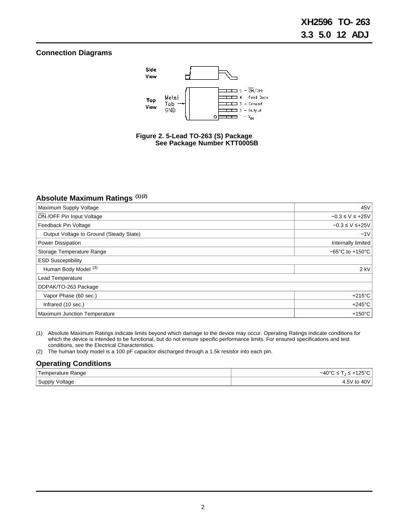
Connection Diagrams
Figure 2. 5-Lead TO-263 (S) PackageSee Package Number KTT0005B
Absolute Maximum Ratings (1) (2)
Maximum Supply Voltage 45V
ON /OFF Pin Input Voltage −0.3 ≤ V ≤ +25V
Feedback Pin Voltage −0.3 ≤ V ≤+25V
Output Voltage to Ground (Steady State) −1V
Power Dissipation Internally limited
Storage Temperature Range −65°C to +150°C
ESD Susceptibility
Human Body Model (3) 2 kV
Lead Temperature
DDPAK/TO-263 Package
Vapor Phase (60 sec.) +215°C
Infrared (10 sec.) +245°C
Maximum Junction Temperature +150°C
(1) Absolute Maximum Ratings indicate limits beyond which damage to the device may occur. Operating Ratings indicate conditions forwhich the device is intended to be functional, but do not ensure specific performance limits. For ensured specifications and testconditions, see the Electrical Characteristics.
(2) The human body model is a 100 pF capacitor discharged through a 1.5k resistor into each pin.
Operating ConditionsTemperature Range −40°C ≤ TJ ≤ +125°C
Supply Voltage 4.5V to 40V
2
XH2596 TO-263 3.3 5.0 12 ADJ

XH2596-3.3 Electrical CharacteristicsSpecifications with standard type face are for TJ = 25°C, and those with boldface type apply over full OperatingTemperature Range
XH2596-3.3UnitsSymbol Parameter Conditions Typ Limit (Limits)(1) (2)
SYSTEM PARAMETERS (3) Test Circuit Figure 20
VOUT Output Voltage 4.75V ≤ VIN ≤ 40V, 0.2A ≤ ILOAD ≤ 3A 3.3 V
3.168/3.135 V(min)
3.432/3.465 V(max)
η Efficiency VIN = 12V, ILOAD = 3A 73 %
(1) Typical numbers are at 25°C and represent the most likely norm.(2) All limits specified at room temperature (standard type face) and at temperature extremes (bold type face). All room temperature limits
are 100% production tested. All limits at temperature extremes are ensured via correlation using standard Statistical Quality Control(SQC) methods. All limits are used to calculate Average Outgoing Quality Level (AOQL).
(3) External components such as the catch diode, inductor, input and output capacitors, and voltage programming resistors can affectswitching regulator system performance. When the XH2596 is used as shown in the Figure 20 test circuit, system performance will beas shown in system parameters of Electrical Characteristics section.
XH2596-5.0 Electrical CharacteristicsSpecifications with standard type face are for TJ = 25°C, and those with boldface type apply over full OperatingTemperature Range
XH2596-5.0UnitsSymbol Parameter Conditions Typ Limit (Limits)(1) (2)
SYSTEM PARAMETERS (3) Test Circuit Figure 20
VOUT Output Voltage 7V ≤ VIN ≤ 40V, 0.2A ≤ ILOAD ≤ 3A 5.0 V
4.800/4.750 V(min)
5.200/5.250 V(max)
η Efficiency VIN = 12V, ILOAD = 3A 80 %
(1) Typical numbers are at 25°C and represent the most likely norm.(2) All limits specified at room temperature (standard type face) and at temperature extremes (bold type face). All room temperature limits
are 100% production tested. All limits at temperature extremes are ensured via correlation using standard Statistical Quality Control(SQC) methods. All limits are used to calculate Average Outgoing Quality Level (AOQL).
(3) External components such as the catch diode, inductor, input and output capacitors, and voltage programming resistors can affectswitching regulator system performance. When the XH2596 is used as shown in the Figure 20 test circuit, system performance will beas shown in system parameters of Electrical Characteristics section.
XH2596-12 Electrical CharacteristicsSpecifications with standard type face are for TJ = 25°C, and those with boldface type apply over full OperatingTemperature Range
XH2596-12UnitsSymbol Parameter Conditions Typ Limit (Limits)(1) (2)
SYSTEM PARAMETERS (3) Test Circuit Figure 20
VOUT Output Voltage 15V ≤ VIN ≤ 40V, 0.2A ≤ ILOAD ≤ 3A 12.0 V
11.52/11.40 V(min)
12.48/12.60 V(max)
η Efficiency VIN = 25V, ILOAD = 3A 90 %
(1) Typical numbers are at 25°C and represent the most likely norm.(2) All limits specified at room temperature (standard type face) and at temperature extremes (bold type face). All room temperature limits
are 100% production tested. All limits at temperature extremes are ensured via correlation using standard Statistical Quality Control(SQC) methods. All limits are used to calculate Average Outgoing Quality Level (AOQL).
(3) External components such as the catch diode, inductor, input and output capacitors, and voltage programming resistors can affectswitching regulator system performance. When the XH2596 is used as shown in the Figure 20 test circuit, system performance will beas shown in system parameters of Electrical Characteristics section.
3
XH2596 TO-263 3.3 5.0 12 ADJ

XH2596-ADJ Electrical CharacteristicsSpecifications with standard type face are for TJ = 25°C, and those with boldface type apply over full OperatingTemperature Range
XH2596-ADJUnitsSymbol Parameter Conditions Typ Limit (Limits)(1) (2)
SYSTEM PARAMETERS (3) Test Circuit Figure 20
VFB Feedback Voltage 4.5V ≤ VIN ≤ 40V, 0.2A ≤ ILOAD ≤ 3A 1.230 V
VOUT programmed for 3V. Circuit of Figure 20 1.193/1.180 V(min)
1.267/1.280 V(max)
η Efficiency VIN = 12V, VOUT = 3V, ILOAD = 3A 73 %
(1) Typical numbers are at 25°C and represent the most likely norm.(2) All limits specified at room temperature (standard type face) and at temperature extremes (bold type face). All room temperature limits
are 100% production tested. All limits at temperature extremes are ensured via correlation using standard Statistical Quality Control(SQC) methods. All limits are used to calculate Average Outgoing Quality Level (AOQL).
(3) External components such as the catch diode, inductor, input and output capacitors, and voltage programming resistors can affectswitching regulator system performance. When the XH2596 is used as shown in the Figure 20 test circuit, system performance will beas shown in system parameters of Electrical Characteristics section.
All Output Voltage Versions Electrical CharacteristicsSpecifications with standard type face are for TJ = 25°C, and those with boldface type apply over full OperatingTemperature Range. Unless otherwise specified, VIN = 12V for the 3.3V, 5V, and Adjustable version and VIN = 24V for the12V version. ILOAD = 500 mA
XH2596-XXUnitsSymbol Parameter Conditions Typ Limit (Limits)(1) (2)
DEVICE PARAMETERS
Ib Feedback Bias Current Adjustable Version Only, VFB = 1.3V 10 nA
50/100 nA (max)
fO Oscillator Frequency See (3) 150 kHz
127/110 kHz(min)
173/173 kHz(max)
VSAT Saturation Voltage IOUT = 3A (4) (5) 1.16 V
1.4/1.5 V(max)
DC Max Duty Cycle (ON) See (5) 100 %
Min Duty Cycle (OFF) See (6) 0
ICL Current Limit Peak Current (4) (5) 4.5 A
3.6/3.4 A(min)
6.9/7.5 A(max)
IL Output Leakage Current Output = 0V (4) (6) 50 μA(max)
Output = −1V (7) 2 mA
30 mA(max)
IQ Quiescent Current See (6) 5 mA
10 mA(max)
(1) Typical numbers are at 25°C and represent the most likely norm.(2) All limits specified at room temperature (standard type face) and at temperature extremes (bold type face). All room temperature limits
are 100% production tested. All limits at temperature extremes are ensured via correlation using standard Statistical Quality Control(SQC) methods. All limits are used to calculate Average Outgoing Quality Level (AOQL).
(3) The switching frequency is reduced when the second stage current limit is activated.(4) No diode, inductor or capacitor connected to output pin.(5) Feedback pin removed from output and connected to 0V to force the output transistor switch ON.(6) Feedback pin removed from output and connected to 12V for the 3.3V, 5V, and the ADJ. version, and 15V for the 12V version, to force
the output transistor switch OFF.(7) VIN = 40V.
4
XH2596 TO-263 3.3 5.0 12 ADJ

All Output Voltage Versions Electrical Characteristics (continued)Specifications with standard type face are for TJ = 25°C, and those with boldface type apply over full OperatingTemperature Range. Unless otherwise specified, VIN = 12V for the 3.3V, 5V, and Adjustable version and VIN = 24V for the12V version. ILOAD = 500 mA
XH2596-XXUnitsSymbol Parameter Conditions Typ Limit (Limits)(1) (2)
ISTBY Standby Quiescent Current ON/OFF pin = 5V (OFF) (7) 80 μA
200/250 μA(max)
θJC Thermal Resistance 2 °C/W
θJA 50 °C/W
θJA
TO-263 Package, Junction to Ambient (9)
50 °C/W
θJA
TO-263 Package, Junction to Ambient (10)
30 °C/W
θJA
TO-263 Package, Junction to Ambient (11)
20 °C/W
ON/OFF CONTROL Test Circuit Figure 20
ON /OFF Pin Logic Input 1.3 V
VIH Threshold Voltage Low (Regulator ON) 0.6 V(max)
VIL High (Regulator OFF) 2.0 V(min)
IH ON /OFF Pin Input Current VLOGIC = 2.5V (Regulator OFF) 5 μA
15 μA(max)
IL VLOGIC = 0.5V (Regulator ON) 0.02 μA
5 μA(max)
(9) Junction to ambient thermal resistance with the TO-263 package tab soldered to a single printed circuit board with 0.5 in2 of (1 oz.)copper area.
(10) Junction to ambient thermal resistance with the TO-263 package tab soldered to a single sided printed circuit board with 2.5 in2 of (1oz.) copper area.
(11) Junction to ambient thermal resistance with the TO-263 package tab soldered to a double sided printed circuit board with 3 in2 of (1 oz.)copper area on the XH2596S side of the board, and approximately 16 in2 of copper on the other side of the p-c board. See ApplicationInformation in this data sheet and the thermal model in Switchers Made Simple™ version 4.3 software.
5
XH2596 TO-263 3.3 5.0 12 ADJ

Typical Performance Characteristics(Circuit of Figure 20)
NormalizedOutput Voltage Line Regulation
Figure 3. Figure 4.
Switch SaturationEfficiency Voltage
Figure 5. Figure 6.
Switch Current Limit Dropout Voltage
Figure 7. Figure 8.
6
XH2596 TO-263 3.3 5.0 12 ADJ

Typical Performance Characteristics (continued)(Circuit of Figure 20)
Operating ShutdownQuiescent Current Quiescent Current
Figure 9. Figure 10.
Minimum Operating ON /OFF ThresholdSupply Voltage Voltage
Figure 11. Figure 12.
ON /OFF PinCurrent (Sinking) Switching Frequency
Figure 13. Figure 14.
7
XH2596 TO-263 3.3 5.0 12 ADJ

Typical Performance Characteristics (continued)(Circuit of Figure 20)
Continuous Mode Switching WaveformsFeedback Pin VIN = 20V, VOUT = 5V, ILOAD = 2ABias Current L = 32 μH, COUT = 220 μF, COUT ESR = 50 mΩ
A: Output Pin Voltage, 10V/div.B: Inductor Current 1A/div.C: Output Ripple Voltage, 50 mV/div.
Figure 15. Figure 16. Horizontal Time Base: 2 μs/div.
Discontinuous Mode Switching Waveforms Load Transient Response for Continuous ModeVIN = 20V, VOUT = 5V, ILOAD = 500 mA VIN = 20V, VOUT = 5V, ILOAD = 500 mA to 2A
L = 10 μH, COUT = 330 μF, COUT ESR = 45 mΩ L = 32 μH, COUT = 220 μF, COUT ESR = 50 mΩ
A: Output Voltage, 100 mV/div. (AC)A: Output Pin Voltage, 10V/div.
B: 500 mA to 2A Load PulseB: Inductor Current 0.5A/div.C: Output Ripple Voltage, 100 mV/div.
Figure 17. Horizontal Time Base: 2 μs/div. Figure 18. Horizontal Time Base: 100 μs/div.
Load Transient Response for Discontinuous ModeVIN = 20V, VOUT = 5V, ILOAD = 500 mA to 2A
L = 10 μH, COUT = 330 μF, COUT ESR = 45 mΩ
A: Output Voltage, 100 mV/div. (AC)B: 500 mA to 2A Load Pulse
Figure 19. Horizontal Time Base: 200 μs/div.
8
XH2596 TO-263 3.3 5.0 12 ADJ

Test Circuit and Layout Guidelines
Fixed Output Voltage Versions
CIN —470 μF, 50V, Aluminum Electrolytic Nichicon “PL Series”COUT —220 μF, 25V Aluminum Electrolytic, Nichicon “PL Series”D1 —5A, 40V Schottky Rectifier, 1N5825L1 —68 μH, L38
Adjustable Output Voltage Versions
where VREF = 1.23V
Select R1 to be approximately 1 kΩ, use a 1% resistor for best stability.CIN —470 μF, 50V, Aluminum Electrolytic Nichicon “PL Series”COUT —220 μF, 35V Aluminum Electrolytic, Nichicon “PL Series”D1 —5A, 40V Schottky Rectifier, 1N5825L1 —68 μH, L38R1 —1 kΩ, 1%CFF —See Application Information Section
Figure 20. Standard Test Circuits and Layout Guides
As in any switching regulator, layout is very important. Rapidly switching currents associated with wiringinductance can generate voltage transients which can cause problems. For minimal inductance and groundloops, the wires indicated by heavy lines should be wide printed circuit traces and should be kept as shortas possible. For best results, external components should be located as close to the switcher lC as possibleusing ground plane construction or single point grounding.
If open core inductors are used, special care must be taken as to the location and positioning of this type ofinductor. Allowing the inductor flux to intersect sensitive feedback, lC groundpath and COUT wiring can causeproblems.
When using the adjustable version, special care must be taken as to the location of the feedback resistors andthe associated wiring. Physically locate both resistors near the IC, and route the wiring away from the inductor,especially an open core type of inductor. (See Application Information section for more information.)
9
XH2596 TO-263 3.3 5.0 12 ADJ
XH2596
XH2596

XH2596 Series Buck Regulator Design Procedure (Fixed Output)
PROCEDURE (Fixed Output Voltage Version) EXAMPLE (Fixed Output Voltage Version)
Given: Given:
VOUT = Regulated Output Voltage (3.3V, 5V or 12V) VOUT = 5V
VIN(max) = Maximum DC Input Voltage VIN(max) = 12V
ILOAD(max) = Maximum Load Current ILOAD(max) = 3A
1. Inductor Selection (L1) 1. Inductor Selection (L1)
A. Select the correct inductor value selection guide from Figures A. Use the inductor selection guide for the 5V version shown inFigure 21, Figure 22, or Figure 23. (Output voltages of 3.3V, 5V, or Figure 22.12V respectively.) For all other voltages, see the Design Procedure B. From the inductor value selection guide shown in Figure 22, thefor the adjustable version. inductance region intersected by the 12V horizontal line and the 3AB. From the inductor value selection guide, identify the inductance vertical line is 33 μH, and the inductor code is L40.region intersected by the Maximum Input Voltage line and the C. The inductance value required is 33 μH. From the table inMaximum Load Current line. Each region is identified by an Table 3, go to the L40 line and choose an inductor part number frominductance value and an inductor code (LXX). any of the four manufacturers shown. (In most instance, bothC. Select an appropriate inductor from the four manufacturer's part through hole and surface mount inductors are available.)numbers listed in Table 3.
2. Output Capacitor Selection (COUT) 2. Output Capacitor Selection (COUT)
A. In the majority of applications, low ESR (Equivalent Series A. See section on output capacitors in Application InformationResistance) electrolytic capacitors between 82 μF and 820 μF and section.low ESR solid tantalum capacitors between 10 μF and 470 μF B. From the quick design component selection table shown inprovide the best results. This capacitor should be located close to Table 1, locate the 5V output voltage section. In the load currentthe IC using short capacitor leads and short copper traces. Do not column, choose the load current line that is closest to the currentuse capacitors larger than 820 μF . needed in your application, for this example, use the 3A line. In theFor additional information, see section on output capacitors in maximum input voltage column, select the line that covers the inputApplication Information section. voltage needed in your application, in this example, use the 15V line.
Continuing on this line are recommended inductors and capacitorsB. To simplify the capacitor selection procedure, refer to the quickthat will provide the best overall performance.design component selection table shown in Table 1. This table
contains different input voltages, output voltages, and load currents, The capacitor list contains both through hole electrolytic and surfaceand lists various inductors and output capacitors that will provide the mount tantalum capacitors from four different capacitorbest design solutions. manufacturers. It is recommended that both the manufacturers and
the manufacturer's series that are listed in the table be used.C. The capacitor voltage rating for electrolytic capacitors should beat least 1.5 times greater than the output voltage, and often much In this example aluminum electrolytic capacitors from severalhigher voltage ratings are needed to satisfy the low ESR different manufacturers are available with the range of ESR numbersrequirements for low output ripple voltage. needed.
D. For computer aided design software, see Switchers Made 330 μF 35V Panasonic HFQ SeriesSimple™ version 4.3 or later. 330 μF 35V Nichicon PL Series
C. For a 5V output, a capacitor voltage rating at least 7.5V or moreis needed. But even a low ESR, switching grade, 220 μF 10Valuminum electrolytic capacitor would exhibit approximately 225 mΩof ESR (see the curve in Figure 26 for the ESR vs voltage rating).This amount of ESR would result in relatively high output ripplevoltage. To reduce the ripple to 1% of the output voltage, or less, acapacitor with a higher value or with a higher voltage rating (lowerESR) should be selected. A 16V or 25V capacitor will reduce theripple voltage by approximately half.
10
XH2596 TO-263 3.3 5.0 12 ADJ

PROCEDURE (Fixed Output Voltage Version) EXAMPLE (Fixed Output Voltage Version)
3. Catch Diode Selection (D1) 3. Catch Diode Selection (D1)
A. The catch diode current rating must be at least 1.3 times greater A. Refer to the table shown in Table 6. In this example, a 5A, 20V,than the maximum load current. Also, if the power supply design 1N5823 Schottky diode will provide the best performance, and willmust withstand a continuous output short, the diode should have a not be overstressed even for a shorted output.current rating equal to the maximum current limit of the XH2596. Themost stressful condition for this diode is an overload or shortedoutput condition.
B. The reverse voltage rating of the diode should be at least 1.25times the maximum input voltage.
C. This diode must be fast (short reverse recovery time) and must belocated close to the XH2596 using short leads and short printedcircuit traces. Because of their fast switching speed and low forwardvoltage drop, Schottky diodes provide the best performance andefficiency, and should be the first choice, especially in low outputvoltage applications. Ultra-fast recovery, or High-Efficiency rectifiersalso provide good results. Ultra-fast recovery diodes typically havereverse recovery times of 50 ns or less. Rectifiers such as the1N5400 series are much too slow and should not be used.
4. Input Capacitor (CIN) 4. Input Capacitor (CIN)
A low ESR aluminum or tantalum bypass capacitor is needed The important parameters for the Input capacitor are the inputbetween the input pin and ground pin to prevent large voltage voltage rating and the RMS current rating. With a nominal inputtransients from appearing at the input. This capacitor should be voltage of 12V, an aluminum electrolytic capacitor with a voltagelocated close to the IC using short leads. In addition, the RMS rating greater than 18V (1.5 × VIN) would be needed. The nextcurrent rating of the input capacitor should be selected to be at least higher capacitor voltage rating is 25V.½ the DC load current. The capacitor manufacturers data sheet must The RMS current rating requirement for the input capacitor in a buckbe checked to assure that this current rating is not exceeded. The regulator is approximately ½ the DC load current. In this example,curve shown in Figure 25 shows typical RMS current ratings for with a 3A load, a capacitor with a RMS current rating of at least 1.5Aseveral different aluminum electrolytic capacitor values. is needed. The curves shown in Figure 25 can be used to select anFor an aluminum electrolytic, the capacitor voltage rating should be appropriate input capacitor. From the curves, locate the 35V line andapproximately 1.5 times the maximum input voltage. Caution must note which capacitor values have RMS current ratings greater thanbe exercised if solid tantalum capacitors are used (see Application 1.5A. A 680 μF/35V capacitor could be used.Information on input capacitor). The tantalum capacitor voltage rating For a through hole design, a 680 μF/35V electrolytic capacitorshould be 2 times the maximum input voltage and it is recommended (Panasonic HFQ series or Nichicon PL series or equivalent) wouldthat they be surge current tested by the manufacturer. be adequate. other types or other manufacturers capacitors can beUse caution when using ceramic capacitors for input bypassing, used provided the RMS ripple current ratings are adequate.because it may cause severe ringing at the VIN pin. For surface mount designs, solid tantalum capacitors can be used,For additional information, see section on input capacitors in but caution must be exercised with regard to the capacitor surgeApplication Information section. current rating (see Application Information on input capacitors in this
data sheet). The TPS series available from AVX, and the 593Dseries from Sprague are both surge current tested.
Table 1. XH2596 Fixed Voltage Quick Design Component Selection Table
Conditions Inductor Output Capacitor
Through Hole Electrolytic Surface Mount Tantalum
Output Load Max Input Panasonic Nichicon AVX TPS SpragueInductance InductorVoltage Current Voltage HFQ Series PL Series Series 595D Series(μH) (#)(V) (A) (V) (μF/V) (μF/V) (μF/V) (μF/V)
3.3 3 5 22 L41 470/25 560/16 330/6.3 390/6.3
7 22 L41 560/35 560/35 330/6.3 390/6.3
10 22 L41 680/35 680/35 330/6.3 390/6.3
40 33 L40 560/35 470/35 330/6.3 390/6.3
6 22 L33 470/25 470/35 330/6.3 390/6.3
2 10 33 L32 330/35 330/35 330/6.3 390/6.3
40 47 L39 330/35 270/50 220/10 330/10
11
XH2596 TO-263 3.3 5.0 12 ADJ
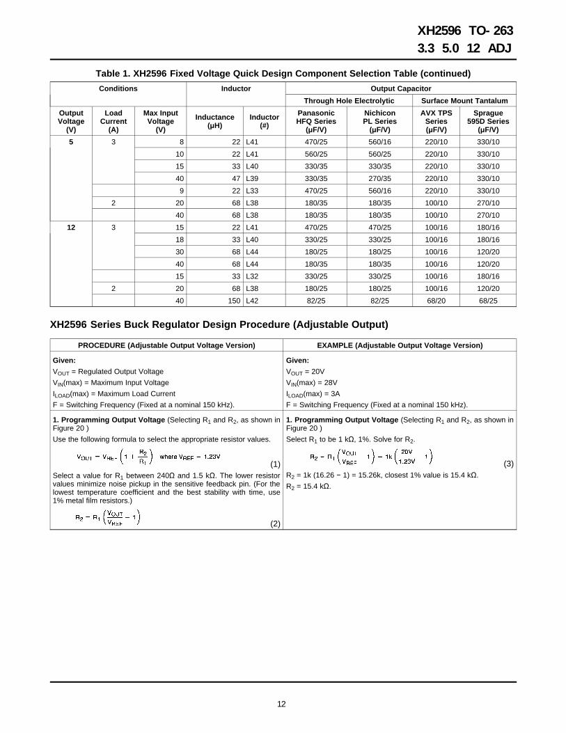
Table 1. XH2596 Fixed Voltage Quick Design Component Selection Table (continued)
Conditions Inductor Output Capacitor
Through Hole Electrolytic Surface Mount Tantalum
Output Load Max Input Panasonic Nichicon AVX TPS SpragueInductance InductorVoltage Current Voltage HFQ Series PL Series Series 595D Series(μH) (#)(V) (A) (V) (μF/V) (μF/V) (μF/V) (μF/V)
5 3 8 22 L41 470/25 560/16 220/10 330/10
10 22 L41 560/25 560/25 220/10 330/10
15 33 L40 330/35 330/35 220/10 330/10
40 47 L39 330/35 270/35 220/10 330/10
9 22 L33 470/25 560/16 220/10 330/10
2 20 68 L38 180/35 180/35 100/10 270/10
40 68 L38 180/35 180/35 100/10 270/10
12 3 15 22 L41 470/25 470/25 100/16 180/16
18 33 L40 330/25 330/25 100/16 180/16
30 68 L44 180/25 180/25 100/16 120/20
40 68 L44 180/35 180/35 100/16 120/20
15 33 L32 330/25 330/25 100/16 180/16
2 20 68 L38 180/25 180/25 100/16 120/20
40 150 L42 82/25 82/25 68/20 68/25
XH2596 Series Buck Regulator Design Procedure (Adjustable Output)
PROCEDURE (Adjustable Output Voltage Version) EXAMPLE (Adjustable Output Voltage Version)
Given: Given:
VOUT = Regulated Output Voltage VOUT = 20V
VIN(max) = Maximum Input Voltage VIN(max) = 28V
ILOAD(max) = Maximum Load Current ILOAD(max) = 3A
F = Switching Frequency (Fixed at a nominal 150 kHz). F = Switching Frequency (Fixed at a nominal 150 kHz).
1. Programming Output Voltage (Selecting R1 and R2, as shown in 1. Programming Output Voltage (Selecting R1 and R2, as shown inFigure 20 ) Figure 20 )
Use the following formula to select the appropriate resistor values. Select R1 to be 1 kΩ, 1%. Solve for R2.
(3)(1)R2 = 1k (16.26 − 1) = 15.26k, closest 1% value is 15.4 kΩ.Select a value for R1 between 240Ω and 1.5 kΩ. The lower resistor
values minimize noise pickup in the sensitive feedback pin. (For the R2 = 15.4 kΩ.lowest temperature coefficient and the best stability with time, use1% metal film resistors.)
(2)
12
XH2596 TO-263 3.3 5.0 12 ADJ

PROCEDURE (Adjustable Output Voltage Version) EXAMPLE (Adjustable Output Voltage Version)
2. Inductor Selection (L1) 2. Inductor Selection (L1)
A. Calculate the inductor Volt • microsecond constant E • T (V • μs), A. Calculate the inductor Volt • microsecond constantfrom the following formula: (E • T),
where(5)
• VSAT = internal switch saturation voltage = B. E • T = 34.2 (V • μs)1.16V
C. ILOAD(max) = 3A• VD = diode forward voltage drop = 0.5V (4)
D. From the inductor value selection guide shown in Figure 24, theinductance region intersected by the 34 (V • μs) horizontal line andthe 3A vertical line is 47 μH, and the inductor code is L39.B. Use the E • T value from the previous formula and match it with
the E • T number on the vertical axis of the Inductor Value Selection E. From the table in Table 3, locate line L39, and select an inductorGuide shown in Figure 24. part number from the list of manufacturers part numbers.C. on the horizontal axis, select the maximum load current.
D. Identify the inductance region intersected by the E • T value andthe Maximum Load Current value. Each region is identified by aninductance value and an inductor code (LXX).
E. Select an appropriate inductor from the four manufacturer's partnumbers listed in Table 3.
3. Output Capacitor Selection (COUT) 3. Output Capacitor SeIection (COUT)
A. In the majority of applications, low ESR electrolytic or solid A. See section on COUT in Application Information section.tantalum capacitors between 82 μF and 820 μF provide the best B. From the quick design table shown in Table 2, locate the outputresults. This capacitor should be located close to the IC using short voltage column. From that column, locate the output voltage closestcapacitor leads and short copper traces. Do not use capacitors to the output voltage in your application. In this example, select thelarger than 820 μF. For additional information, see section on 24V line. Under the OUTPUT CAPACITOR section, select aoutput capacitors in Application Information section. capacitor from the list of through hole electrolytic or surface mountB. To simplify the capacitor selection procedure, refer to the quick tantalum types from four different capacitor manufacturers. It isdesign table shown in Table 2. This table contains different output recommended that both the manufacturers and the manufacturersvoltages, and lists various output capacitors that will provide the best series that are listed in the table be used.design solutions. In this example, through hole aluminum electrolytic capacitors fromC. The capacitor voltage rating should be at least 1.5 times greater several different manufacturers are available.than the output voltage, and often much higher voltage ratings are 220 μF/35V Panasonic HFQ Seriesneeded to satisfy the low ESR requirements needed for low output
150 μF/35V Nichicon PL Seriesripple voltage.C. For a 20V output, a capacitor rating of at least 30V or more isneeded. In this example, either a 35V or 50V capacitor would work.A 35V rating was chosen, although a 50V rating could also be usedif a lower output ripple voltage is needed.
Other manufacturers or other types of capacitors may also be used,provided the capacitor specifications (especially the 100 kHz ESR)closely match the types listed in the table. Refer to the capacitormanufacturers data sheet for this information.
4. Feedforward Capacitor (CFF) (See Figure 20) 4. Feedforward Capacitor (CFF)
For output voltages greater than approximately 10V, an additional The table shown in Table 2 contains feed forward capacitor valuescapacitor is required. The compensation capacitor is typically for various output voltages. In this example, a 560 pF capacitor isbetween 100 pF and 33 nF, and is wired in parallel with the output needed.voltage setting resistor, R2. It provides additional stability for highoutput voltages, low input-output voltages, and/or very low ESRoutput capacitors, such as solid tantalum capacitors.
(6)This capacitor type can be ceramic, plastic, silver mica, etc.(Because of the unstable characteristics of ceramic capacitors madewith Z5U material, they are not recommended.)
13
XH2596 TO-263 3.3 5.0 12 ADJ

PROCEDURE (Adjustable Output Voltage Version) EXAMPLE (Adjustable Output Voltage Version)
5. Catch Diode Selection (D1) 5. Catch Diode Selection (D1)
A. The catch diode current rating must be at least 1.3 times greater A. Refer to the table shown in Table 6. Schottky diodes provide thethan the maximum load current. Also, if the power supply design best performance, and in this example a 5A, 40V, 1N5825 Schottkymust withstand a continuous output short, the diode should have a diode would be a good choice. The 5A diode rating is more thancurrent rating equal to the maximum current limit of the XH2596. The adequate and will not be overstressed even for a shorted output.most stressful condition for this diode is an overload or shortedoutput condition.
B. The reverse voltage rating of the diode should be at least 1.25times the maximum input voltage.
C. This diode must be fast (short reverse recovery time) and must belocated close to the XH2596 using short leads and short printedcircuit traces. Because of their fast switching speed and low forwardvoltage drop, Schottky diodes provide the best performance andefficiency, and should be the first choice, especially in low outputvoltage applications. Ultra-fast recovery, or High-Efficiency rectifiersare also a good choice, but some types with an abrupt turn-offcharacteristic may cause instability or EMl problems. Ultra-fastrecovery diodes typically have reverse recovery times of 50 ns orless. Rectifiers such as the 1N4001 series are much too slow andshould not be used.
6. Input Capacitor (CIN) 6. Input Capacitor (CIN)
A low ESR aluminum or tantalum bypass capacitor is needed The important parameters for the Input capacitor are the inputbetween the input pin and ground to prevent large voltage transients voltage rating and the RMS current rating. With a nominal inputfrom appearing at the input. In addition, the RMS current rating of voltage of 28V, an aluminum electrolytic aluminum electrolyticthe input capacitor should be selected to be at least ½ the DC load capacitor with a voltage rating greater than 42V (1.5 × VIN) would becurrent. The capacitor manufacturers data sheet must be checked to needed. Since the the next higher capacitor voltage rating is 50V, aassure that this current rating is not exceeded. The curve shown in 50V capacitor should be used. The capacitor voltage rating of (1.5 ×Figure 25 shows typical RMS current ratings for several different VIN) is a conservative guideline, and can be modified somewhat ifaluminum electrolytic capacitor values. desired.
This capacitor should be located close to the IC using short leads The RMS current rating requirement for the input capacitor of a buckand the voltage rating should be approximately 1.5 times the regulator is approximately ½ the DC load current. In this example,maximum input voltage. with a 3A load, a capacitor with a RMS current rating of at least 1.5A
is needed.If solid tantalum input capacitors are used, it is recomended that theybe surge current tested by the manufacturer. The curves shown in Figure 25 can be used to select an appropriate
input capacitor. From the curves, locate the 50V line and note whichUse caution when using a high dielectric constant ceramic capacitorcapacitor values have RMS current ratings greater than 1.5A. Eitherfor input bypassing, because it may cause severe ringing at the VIN a 470 μF or 680 μF, 50V capacitor could be used.pin.For a through hole design, a 680 μF/50V electrolytic capacitorFor additional information, see section on input capacitors in(Panasonic HFQ series or Nichicon PL series or equivalent) wouldApplication Information section.be adequate. Other types or other manufacturers capacitors can beused provided the RMS ripple current ratings are adequate.
For surface mount designs, solid tantalum capacitors can be used,but caution must be exercised with regard to the capacitor surgecurrent rting (see Application Information or input capacitors in thisdata sheet). The TPS series available from AVX, and the 593Dseries from Sprague are both surge current tested.
To further simplify the buck regulator design procedure, TexasInstruments is making available computer design software to beused with the Simple Switcher line ot switching regulators.Switchers Made Simple (version 4.3 or later) is available on a 3½″diskette for IBM compatible computers.
XH2596 Series Buck Regulator Design Procedure (Adjustable Output)
Table 2. Output Capacitor and Feedforward Capacitor Selection Table
Output Through Hole Output Capacitor Surface Mount Output CapacitorVoltage Panasonic Nichicon PL AVX TPS SpragueFeedforward Feedforward(V) HFQ Series Series Series 595D SeriesCapacitor Capacitor(μF/V) (μF/V) (μF/V) (μF/V)
2 820/35 820/35 33 nF 330/6.3 470/4 33 nF
4 560/35 470/35 10 nF 330/6.3 390/6.3 10 nF
6 470/25 470/25 3.3 nF 220/10 330/10 3.3 nF
14
XH2596 TO-263 3.3 5.0 12 ADJ

Table 2. Output Capacitor and Feedforward Capacitor Selection Table (continued)
Output Through Hole Output Capacitor Surface Mount Output CapacitorVoltage Panasonic Nichicon PL AVX TPS SpragueFeedforward Feedforward(V) HFQ Series Series Series 595D SeriesCapacitor Capacitor(μF/V) (μF/V) (μF/V) (μF/V)
9 330/25 330/25 1.5 nF 100/16 180/16 1.5 nF
1 2 330/25 330/25 1 nF 100/16 180/16 1 nF
1 5 220/35 220/35 680 pF 68/20 120/20 680 pF
2 4 220/35 150/35 560 pF 33/25 33/25 220 pF
2 8 100/50 100/50 390 pF 10/35 15/50 220 pF
Figure 21. XH2596-3.3 Figure 22. XH2596-5.0
Figure 23. XH2596-12
15
XH2596 TO-263 3.3 5.0 12 ADJ
XHure 24. XH2596-ADJ
(For Continuous Mode Operation)
INDUCTOR VALUE SELECTION GUIDES
XH2596 Series Buck Regulator Design Procedure
