xilinx ise getting started - baylor university ise – getting started 4 9. to place a part on your...
TRANSCRIPT
Xilinx ISE – Getting Started 1
Xilinx ISE – Getting Started
Last updated: 9/19/15, John Miller, Xilinx ISE Project Navigator 14.2
A. Creating a new project
1. Select Start All Programs Development Tools 64-bit Project Navigator. If the startup
tips pop up, click OK to dismiss them.
2. Select File New Project….
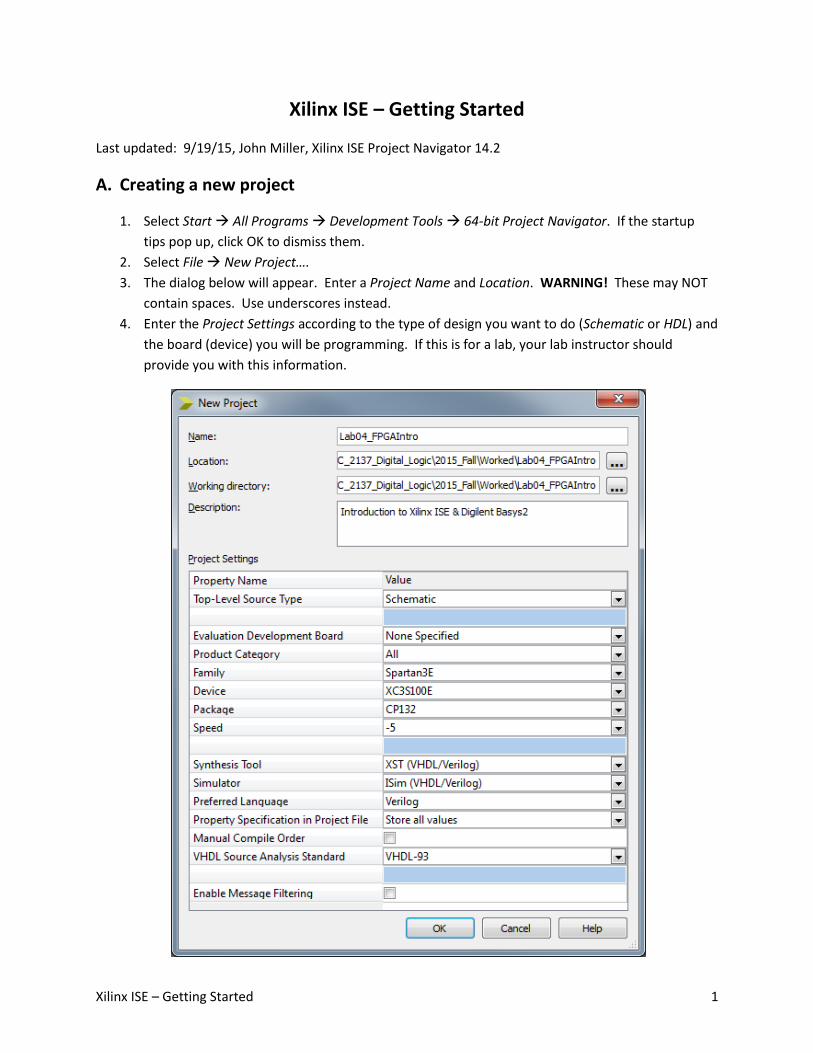
3. The dialog below will appear. Enter a Project Name and Location. WARNING! These may NOT
contain spaces. Use underscores instead.
4. Enter the Project Settings according to the type of design you want to do (Schematic or HDL) and
the board (device) you will be programming. If this is for a lab, your lab instructor should
provide you with this information.
Xilinx ISE – Getting Started 2
B. Navigating Project Navigator
There are four main windows in Project Navigator (see figure below). On the top left is the Hierarchy (or
Sources) window, which displays your project file and all of its source files. When a source file is
selected, all of the processes associated with it appear in the Processes window beneath.
IMPORTANT! Both the Hierarchy and the Processes windows change their function based on which
mode and tab is selected. The mode (or “view”) is located above the Hierarchy window and has two
options: Implementation and Simulation. The tabs are located below the Processes window and there
are many.
On the right is the project workspace. On the bottom is the Transcript window, which displays messages
pertaining to your current process, including errors and warnings. (If your window doesn’t look correct,
be sure that the Design tab in the lower left [above the word “Console”] is selected.)
Note: You can close windows/tabs that are not needed, such as the Start, Files, and Libraries tabs.
Closed windows/tabs can be re-opened from the View menu. If there are too many tabs to display at
one time, an arrow ► will appear. Clicking it will scroll through the tabs.
Hierarchy – lists
project files
Process – steps in the
implementation
process
Switch between Implementation and Simulation views (or modes)
Main Window –
this image shows
the schematic
editor
Transcript – displays
notes, errors, and
warning
Schematic Editor
toolbar
Tabs – Design, Libraries,
Symbols, etc.

Xilinx ISE – Getting Started 3
C. Creating a new source file
5. Select Project New Source…
6. The dialog below will appear. Select the desired source type, and enter an appropriate File
name. The directory (folder) for you project should appear in the Location box (if not then click
the three dots to find it). Make sure that Add to project is checked, and click Next.
7. Another dialog may appear. Click Finish.
D. Drawing a schematic
When you create a new schematic, Xilinx launches the schematic editor. This
adds a toolbar to the left of the workspace, a couple of tabs to the leftmost
window, and a blank schematic in the workspace. One of the tabs on the left
window is labeled Symbols. The Symbols window is used to select symbols to add
to the schematic. Another tab is labeled Options. The options in the Options
window change depending on which tool you select from the toolbar.
8. Select the Symbols tab. Under the Symbols tab, you will see two lists:
Categories and Symbols. When a category is selected, all of its
symbols/parts/components will appear in the Symbols list. Highlight
various categories (e.g. Logic) and see the types of symbols that can be
added (e.g. basic logic gates like and, or, etc.). For the basic gates, the
number that follows indicates the number of inputs (e.g. “and2” is a 2-
input And gate). “b#” indicates how many inputs have “bubbles” (are
inverted). So, “or5b3” is a 5-input Or gate with 3 inputs inverted.
Xilinx ISE – Getting Started 4
9. To place a part on your schematic, select the part in the Symbols list and move your cursor over
the sheet area. Click to add the part.
Note: When you first add a part, the schematic editor automatically assigns a name to the part
in the form of XLXI_number (Xilinx Instance number). This number does not show up unless you
make it visible. You may double click on the part to change the value of the instance name (e.g.
to “U1”) and make it visible if you wish.
10. To add wire, go to Add Wire (or click the button on the toolbar or Ctrl+W). To connect
parts together, draw lines between component leads. For input and output connections, start
on the pin of a part and draw a wire to some point on the schematic. Press escape to stop
drawing wires if needed.
11. I/O Markers are used to define connections to external pins of the FPGA. I/O markers can only
be attached to wires (i.e., you cannot drop them on the page without connecting them to
anything) so you must first add wire segments for each I/O marker (or connect the I/O Markers
to wires coming from a gate).
To add an I/O Marker, go to Add I/O Marker (or click the button on the toolbar or
Ctrl+G). Move your cursor over the sheet and attach the I/O marker to the appropriate wire. By
default, Xilinx will automatically determine whether the I/O marker should be an input or an
output. If needed, you change the default behavior under the Options tab. You can also change
it after placement. Double-click on an I/O marker. The Object Properties dialog will pop up
allowing you to change the polarity of the port.
Notes about names:
Even if two wires are not visually connected on the schematic, once two wires have the
same name they are connected. This can simplify your schematic greatly, but can also lead
to problems if you’re not careful!
A “branch” is a specific set of wires (e.g. click on a wire, it highlights the branch in red). A
“net” is all of the branches that are connected (i.e. have the same name). For small designs,
there is likely no difference. However, if you make use of the names to electrically connect
wires as mentioned in the previous bullet, then there is a difference.
When you first add a wire or I/O marker, the editor automatically assigns a name to the net
in the form of XLXN_number (Xilinx Net number). To rename your inputs and outputs, right-
click the I/O marker and click Rename Port. In the resulting window, make sure Rename the
Branch's Net is selected (see figure) and then type the new name of the net/wire in the text
field. Click OK. If a message appears asking to merge any nets with the same name, click
Yes.
You can rename wires in the same fashion (right-click, choose Rename Selected Net…). You
must decide whether you want to rename only the branch or the entire net.

Xilinx ISE – Getting Started 5
12. Once you have drawn your schematic, you can check it for errors by selecting Tools Check
Schematic (or click the button on the toolbar). Correct any errors. Don’t forget to Save it!
E. Creating an HDL file (module)
The logic implemented inside of an FPGA can also be defined by a “Hardware Description Language,”
either VHDL or Verilog. (In fact, if you draw a schematic, it actually gets translated to an HDL file before
being “synthesized” and programmed into the FPGA.)
13. Follow the steps above to create a new source file. Choose either “Verilog Module” or “VHDL
Module” (depending on what language you want to use). Name it, and be sure to Add to
project.
14. The Define Module dialog should appear. This allows you to specify the inputs and outputs to
your module (component) and will allow Xilinx to auto-generate some of the code for you.
Enter the appropriate information for your design. The example shown here is a 16-bit, 2-input
multiplexer. It has two 16-bit inputs, one 1-bit select input, and one 16-bit output. Click Next.
This will rename all of the wires
associated with a particular
“net” (i.e. have the same name &
are electrically connected, even
if not drawn on the schematic).
This will rename only the
currently selected “branch” (i.e.
wires physically connected on
schematic).
Xilinx ISE – Getting Started 6
15. A Summary dialog should appear. If everything looks correct, click Finish. The new code file
should appear in the workspace, ready for editing, and in your Hierarchy list.
F. Creating a test bench
A test bench is a special circuit used to stimulate (i.e. provide inputs to) a design during simulation.
Think of it like the equipment on an actual lab bench, providing power and inputs to a hardware circuit
and looking at its outputs.
In order to create a test bench, we have to tell Xilinx how to interact with our circuit. This is done using
either VHDL or Verilog.
16. Follow the steps above to create a new source file. Choose either “Verilog Test Fixure” or “VHDL
Test Bench” (depending on what language you want to use). Name it (see note), and be sure to
Add to project. Click Next.
Note: A good practice is to name your test bench with the same name as the module you want
to test, followed by “_tb”. For instance, I named this one “mux_16bit_tb” to correspond to the
“mux_16bit” file I created in the previous section. This will help you know what file is what, and
it keeps your files grouped alphabetically.
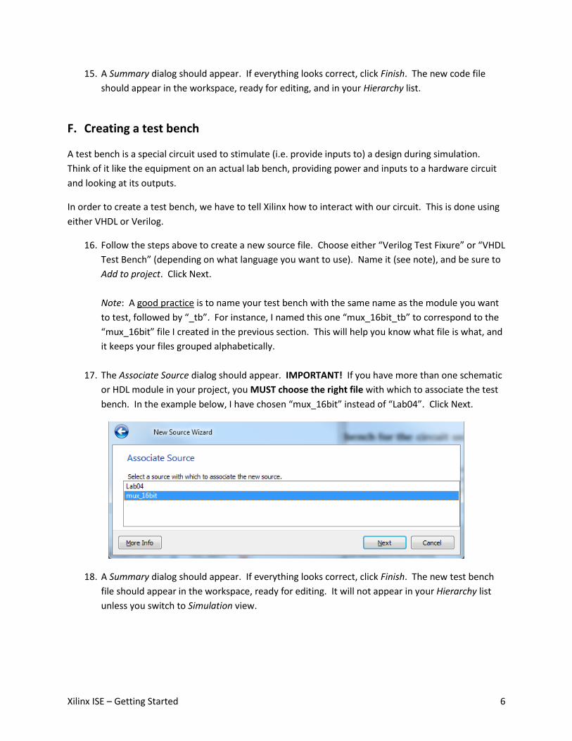
17. The Associate Source dialog should appear. IMPORTANT! If you have more than one schematic
or HDL module in your project, you MUST choose the right file with which to associate the test
bench. In the example below, I have chosen “mux_16bit” instead of “Lab04”. Click Next.
18. A Summary dialog should appear. If everything looks correct, click Finish. The new test bench
file should appear in the workspace, ready for editing. It will not appear in your Hierarchy list
unless you switch to Simulation view.
Xilinx ISE – Getting Started 7
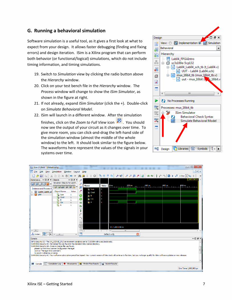
G. Running a behavioral simulation
Software simulation is a useful tool, as it gives a first look at what to
expect from your design. It allows faster debugging (finding and fixing
errors) and design iteration. ISim is a Xilinx program that can perform
both behavior (or functional/logical) simulations, which do not include
timing information, and timing simulations.
19. Switch to Simulation view by clicking the radio button above
the Hierarchy window.
20. Click on your test bench file in the Hierarchy window. The
Process window will change to show the ISim Simulator, as
shown in the figure at right.
21. If not already, expand ISim Simulator (click the +). Double-click
on Simulate Behavioral Model.
22. ISim will launch in a different window. After the simulation
finishes, click on the Zoom to Full View icon . You should now see the output of your circuit as it changes over time. To give more room, you can click-and-drag the left-hand side of the simulation window (almost the middle of the whole window) to the left. It should look similar to the figure below. The waveforms here represent the values of the signals in your systems over time.
Xilinx ISE – Getting Started 8
23. ISim simulates 1000 ns by default. If you created a test bench longer than 1000 ns, you will
need to enter “### ns” in the box in the top right (where ### is the number of
ns of additional time you need the simulator to run) and click the Run for time specified icon to
the left.
24. If you need to modify your test bench or re-run it, you will want to close the ISim window,
return to the Xilinx window, and run Simulate Behavioral Model again.
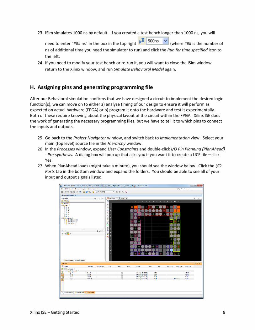
H. Assigning pins and generating programming file
After our Behavioral simulation confirms that we have designed a circuit to implement the desired logic function(s), we can move on to either a) analyze timing of our design to ensure it will perform as expected on actual hardware (FPGA) or b) program it onto the hardware and test it experimentally. Both of these require knowing about the physical layout of the circuit within the FPGA. Xilinx ISE does the work of generating the necessary programming files, but we have to tell it to which pins to connect the inputs and outputs.
25. Go back to the Project Navigator window, and switch back to Implementation view. Select your main (top level) source file in the Hierarchy window.
26. In the Processes window, expand User Constraints and double-click I/O Pin Planning (PlanAhead) - Pre-synthesis. A dialog box will pop up that asks you if you want it to create a UCF file—click Yes.
27. When PlanAhead loads (might take a minute), you should see the window below. Click the I/O Ports tab in the bottom window and expand the folders. You should be able to see all of your input and output signals listed.
Xilinx ISE – Getting Started 9
28. Each of these signals should be associated with an I/O pin. You will need to consult your instructor or the documentation for your development platform to determine which pins are the ones you need (e.g. on the Digilent Basys2, pin P11 is connected to switch SW0).
29. To make the assignments, drag-and-drop the signals from the bottom window onto the appropriate pin circles in the Package window. The pins are arranged in a letter/number grid format.
30. To save your pin assignments select File Save Design from the menu bar (or click the disk icon
). After you save the file, it will appear in the Hierarchy window in Project Navigator underneath the schematic file.
31. Return to the Project Navigator window, and switch to Implementation view. Select your top-level module (schematic or HDL source file). In the Processes window, double-click on Generate Programming File. After running (may take a minute), you should see a line in the Console that says: Process "Generate Programming File" completed successfully.
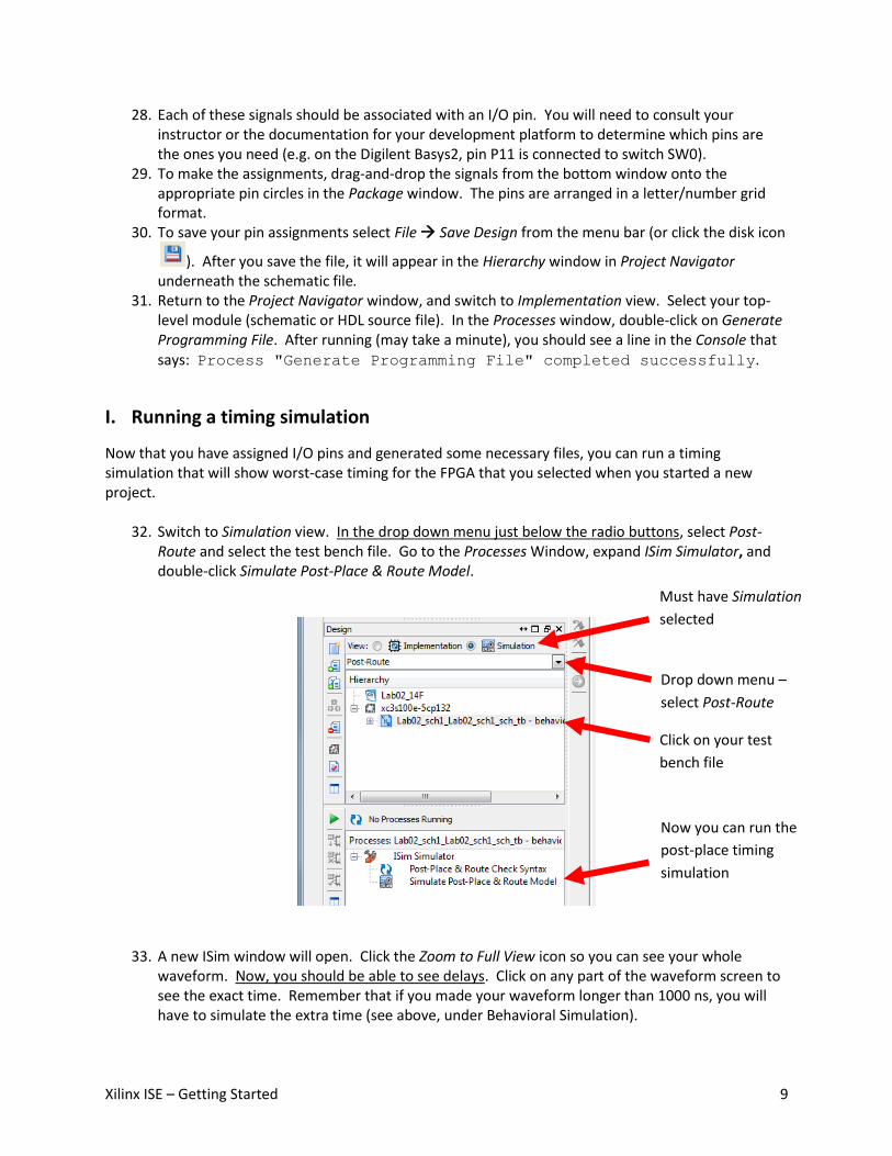
I. Running a timing simulation
Now that you have assigned I/O pins and generated some necessary files, you can run a timing simulation that will show worst-case timing for the FPGA that you selected when you started a new project.
32. Switch to Simulation view. In the drop down menu just below the radio buttons, select Post-Route and select the test bench file. Go to the Processes Window, expand ISim Simulator, and double-click Simulate Post-Place & Route Model.
33. A new ISim window will open. Click the Zoom to Full View icon so you can see your whole waveform. Now, you should be able to see delays. Click on any part of the waveform screen to see the exact time. Remember that if you made your waveform longer than 1000 ns, you will have to simulate the extra time (see above, under Behavioral Simulation).
Must have Simulation
selected
Drop down menu –
select Post-Route
Click on your test
bench file
Now you can run the
post-place timing
simulation

Xilinx ISE – Getting Started 10
J. Implementing your design on an FPGA
Once you have generated the programming (.bit) file, you can load that file onto your FPGA. How this is
done varies from platform to platform (i.e. development board to development board). Here are the
instructions for the Digilent Basys2. Your lab instructor may provide alternative instructions.
Caution! All integrated circuits and boards using them are sensitive to static electricity. To avoid
damaging the boards, make sure that you have grounded yourself before handling the boards and try to
handle the boards by the edges only.
34. Connect the Digilent Basys2 board via the mini USB port to the computer. Move the power switch to the ON position. The power LED should come on, you should see the seven-segment displays changing.
35. Open the Adept software by going to Start All Programs Development Tools Digilent Adept Adept. A window should open that looks like the one below. If the drop down menu in the upper right does not say Basys2, make sure that your board is properly connected, then pull down the menu and select Basys2.
36. Click the top Browse button (across from FPGA) and find the .bit file associated with your project (e.g. “Lab02.bit”). When you open it, you should get a Warning dialog as shown. Click Yes.
Xilinx ISE – Getting Started 11
37. Click Program. You should get the same warning dialog again, so click Yes again. You should get the message Programming Successful.
38. This is the fun part—test your design on the board! Try all possible combinations of inputs and observe the output produced to verify that it works as expected.
39. After you are finished demonstrating your working project and are ready to put up the board, go to the Adept software and click Initialize Chain (in the middle of the window). This will clear the memory for the next person.
K. Documentation
Likely, you will need to capture screen shots for your lab reports. You have two options for this: 1) copy
& paste (“C/P”) directly to Word or 2) save to a pdf for copying later.
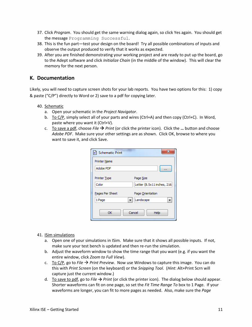
40. Schematic a. Open your schematic in the Project Navigator. b. To C/P, simply select all of your parts and wires (Ctrl+A) and then copy (Ctrl+C). In Word,
paste where you want it (Ctrl+V). c. To save a pdf, choose File Print (or click the printer icon). Click the … button and choose
Adobe PDF. Make sure your other settings are as shown. Click OK, browse to where you want to save it, and click Save.
41. ISim simulations a. Open one of your simulations in ISim. Make sure that it shows all possible inputs. If not,
make sure your test bench is updated and then re-run the simulation. b. Adjust the waveform window to show the time range that you want (e.g. if you want the
entire window, click Zoom to Full View). c. To C/P, go to File Print Preview. Now use Windows to capture this image. You can do
this with Print Screen (on the keyboard) or the Snipping Tool. (Hint: Alt+Print Scrn will capture just the current window.)
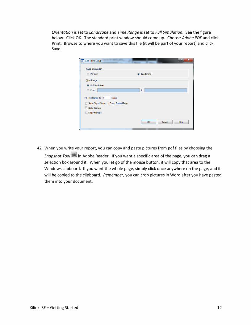
d. To save to pdf, go to File → Print (or click the printer icon). The dialog below should appear. Shorter waveforms can fit on one page, so set the Fit Time Range To box to 1 Page. If your waveforms are longer, you can fit to more pages as needed. Also, make sure the Page
Xilinx ISE – Getting Started 12
Orientation is set to Landscape and Time Range is set to Full Simulation. See the figure below. Click OK. The standard print window should come up. Choose Adobe PDF and click Print. Browse to where you want to save this file (it will be part of your report) and click Save.
42. When you write your report, you can copy and paste pictures from pdf files by choosing the
Snapshot Tool in Adobe Reader. If you want a specific area of the page, you can drag a
selection box around it. When you let go of the mouse button, it will copy that area to the
Windows clipboard. If you want the whole page, simply click once anywhere on the page, and it
will be copied to the clipboard. Remember, you can crop pictures in Word after you have pasted
them into your document.