xmc4100/xmc4200 data sheet - infineon technologies
TRANSCRIPT
Data SheetV1.4 2018-09
Microcontrol lers
XMC4100 / XMC4200Microcontroller Seriesfor Industrial Applications
XMC4000 Family
ARM® Cortex®-M432-bit processor core
Edition 2018-09Published byInfineon Technologies AG81726 Munich, Germany© 2018 Infineon Technologies AGAll Rights Reserved.
Legal DisclaimerThe information given in this document shall in no event be regarded as a guarantee of conditions or characteristics. With respect to any examples or hints given herein, any typical values stated herein and/or any information regarding the application of the device, Infineon Technologies hereby disclaims any and all warranties and liabilities of any kind, including without limitation, warranties of non-infringement of intellectual property rights of any third party.
InformationFor further information on technology, delivery terms and conditions and prices, please contact the nearest Infineon Technologies Office (www.infineon.com).
WarningsDue to technical requirements, components may contain dangerous substances. For information on the types in question, please contact the nearest Infineon Technologies Office.Infineon Technologies components may be used in life-support devices or systems only with the express written approval of Infineon Technologies, if a failure of such components can reasonably be expected to cause the failure of that life-support device or system or to affect the safety or effectiveness of that device or system. Life support devices or systems are intended to be implanted in the human body or to support and/or maintain and sustain and/or protect human life. If they fail, it is reasonable to assume that the health of the user or other persons may be endangered.

Data SheetV1.4 2018-09
Microcontrol lers
XMC4100 / XMC4200Microcontroller Seriesfor Industrial Applications
XMC4000 Family
ARM® Cortex®-M432-bit processor core

XMC4100 / XMC4200XMC4000 Family
Data Sheet V1.4, 2018-09
XMC4[12]00 Data Sheet
Revision History: V1.4 2018-09Previous Versions:V1.3 2015-10V1.2 2014-06V1.1 2014-03V1.0 2013-10V0.6 2012-11Page Subjects43 Added RMS Noise parameter in VADC Parameters table. 12 Added a section listing the packages of the different markings.14 Added BA marking variant.14 Corrected SCU_IDCHIP value of XMC4100 EES-AA/ES-AA.36 Added footnote explaining minimum VBAT requirements to start the
hibernate domain and/or oscillation of a crystal on RTC_XTAL.37 Changed pull device definition to System Requirement (SR) to reflect that
the specified currents are defined by the characteristics of the external load/driver.
37 Added information that PORST Pull-up is identical to the pull-up on standard I/O pins.
42 Updated CAINSW, CAINTOT and RAIN parameters with improved values.56 Added footnote on test configuration for LPAC measurement.58 Corrected parameter name of of USB pull device (upstream port receiving)
definition according to USB standard (referenced to DM instead of DP)62 Relaxed RTC_XTAL VPPX parameter value and changed it to a system
requirement.66 Added footnote on current consumption by enabling of fCCU.67 Added Flash endurance parameter for 64 Kbytes Physical Sector PS4
NEPS4 for devices with BA marking.many Added PG-TQFP-64-19 and PG-VQFN-48-71 package information.89, 90 Added tables describing the differences between PG-LQFP-64-19 to PG-
TQFP-64-19 as well as PG-VQFN-48-53 to PG-VQFN-48-71 packages.92 Updated to JEDEC standard J-STD-020D for the moisture sensitivity level
and added solder temperature parameter according to the same standard.
Subject to Agreement on the Use of Product Information

XMC4100 / XMC4200XMC4000 Family
Data Sheet V1.4, 2018-09
TrademarksC166™, TriCore™, XMC™ and DAVE™ are trademarks of Infineon Technologies AG.ARM®, ARM Powered®, Cortex®, Thumb® and AMBA® are registered trademarks ofARM, Limited.CoreSight™, ETM™, Embedded Trace Macrocell™ and Embedded Trace Buffer™ aretrademarks of ARM, Limited.Synopsys™ is a trademark of Synopsys, Inc.
We Listen to Your CommentsIs there any information in this document that you feel is wrong, unclear or missing?Your feedback will help us to continuously improve the quality of this document.Please send your proposal (including a reference to this document) to:[email protected]
Subject to Agreement on the Use of Product Information

XMC4100 / XMC4200XMC4000 Family
Table of Contents
Data Sheet 6 V1.4, 2018-09
1 Summary of Features . . . . . . . . . . . . . . . . . . . . . . . . . . . . . . . . . . . . . . . . 91.1 Ordering Information . . . . . . . . . . . . . . . . . . . . . . . . . . . . . . . . . . . . . . . . . 111.2 Device Types . . . . . . . . . . . . . . . . . . . . . . . . . . . . . . . . . . . . . . . . . . . . . . . 111.3 Package Variants . . . . . . . . . . . . . . . . . . . . . . . . . . . . . . . . . . . . . . . . . . . . 121.4 Device Type Features . . . . . . . . . . . . . . . . . . . . . . . . . . . . . . . . . . . . . . . . 121.5 Definition of Feature Variants . . . . . . . . . . . . . . . . . . . . . . . . . . . . . . . . . . 131.6 Identification Registers . . . . . . . . . . . . . . . . . . . . . . . . . . . . . . . . . . . . . . . 14
2 General Device Information . . . . . . . . . . . . . . . . . . . . . . . . . . . . . . . . . . 162.1 Logic Symbols . . . . . . . . . . . . . . . . . . . . . . . . . . . . . . . . . . . . . . . . . . . . . . 162.2 Pin Configuration and Definition . . . . . . . . . . . . . . . . . . . . . . . . . . . . . . . . . 182.2.1 Package Pin Summary . . . . . . . . . . . . . . . . . . . . . . . . . . . . . . . . . . . . . 202.2.2 Port I/O Functions . . . . . . . . . . . . . . . . . . . . . . . . . . . . . . . . . . . . . . . . . 242.2.2.1 Port I/O Function Table . . . . . . . . . . . . . . . . . . . . . . . . . . . . . . . . . . . 252.3 Power Connection Scheme . . . . . . . . . . . . . . . . . . . . . . . . . . . . . . . . . . . . 28
3 Electrical Parameters . . . . . . . . . . . . . . . . . . . . . . . . . . . . . . . . . . . . . . . 303.1 General Parameters . . . . . . . . . . . . . . . . . . . . . . . . . . . . . . . . . . . . . . . . . 303.1.1 Parameter Interpretation . . . . . . . . . . . . . . . . . . . . . . . . . . . . . . . . . . . . 303.1.2 Absolute Maximum Ratings . . . . . . . . . . . . . . . . . . . . . . . . . . . . . . . . . . 313.1.3 Pin Reliability in Overload . . . . . . . . . . . . . . . . . . . . . . . . . . . . . . . . . . . 333.1.4 Pad Driver and Pad Classes Summary . . . . . . . . . . . . . . . . . . . . . . . . . 353.1.5 Operating Conditions . . . . . . . . . . . . . . . . . . . . . . . . . . . . . . . . . . . . . . . 363.2 DC Parameters . . . . . . . . . . . . . . . . . . . . . . . . . . . . . . . . . . . . . . . . . . . . . 373.2.1 Input/Output Pins . . . . . . . . . . . . . . . . . . . . . . . . . . . . . . . . . . . . . . . . . . 373.2.2 Analog to Digital Converters (ADCx) . . . . . . . . . . . . . . . . . . . . . . . . . . . 423.2.3 Digital to Analog Converters (DACx) . . . . . . . . . . . . . . . . . . . . . . . . . . . 473.2.4 Out-of-Range Comparator (ORC) . . . . . . . . . . . . . . . . . . . . . . . . . . . . . 503.2.5 High Resolution PWM (HRPWM) . . . . . . . . . . . . . . . . . . . . . . . . . . . . . 523.2.5.1 HRC characteristics . . . . . . . . . . . . . . . . . . . . . . . . . . . . . . . . . . . . . . 523.2.5.2 CMP and 10-bit DAC characteristics . . . . . . . . . . . . . . . . . . . . . . . . . 523.2.5.3 Clocks . . . . . . . . . . . . . . . . . . . . . . . . . . . . . . . . . . . . . . . . . . . . . . . . 553.2.6 Low Power Analog Comparator (LPAC) . . . . . . . . . . . . . . . . . . . . . . . . 563.2.7 Die Temperature Sensor . . . . . . . . . . . . . . . . . . . . . . . . . . . . . . . . . . . . 573.2.8 USB Device Interface DC Characteristics . . . . . . . . . . . . . . . . . . . . . . . 583.2.9 Oscillator Pins . . . . . . . . . . . . . . . . . . . . . . . . . . . . . . . . . . . . . . . . . . . . 593.2.10 Power Supply Current . . . . . . . . . . . . . . . . . . . . . . . . . . . . . . . . . . . . . . 633.2.11 Flash Memory Parameters . . . . . . . . . . . . . . . . . . . . . . . . . . . . . . . . . . 673.3 AC Parameters . . . . . . . . . . . . . . . . . . . . . . . . . . . . . . . . . . . . . . . . . . . . . 693.3.1 Testing Waveforms . . . . . . . . . . . . . . . . . . . . . . . . . . . . . . . . . . . . . . . . 693.3.2 Power-Up and Supply Monitoring . . . . . . . . . . . . . . . . . . . . . . . . . . . . . 703.3.3 Power Sequencing . . . . . . . . . . . . . . . . . . . . . . . . . . . . . . . . . . . . . . . . . 71
Table of Contents
Subject to Agreement on the Use of Product Information

XMC4100 / XMC4200XMC4000 Family
Table of Contents
Data Sheet 7 V1.4, 2018-09
3.3.4 Phase Locked Loop (PLL) Characteristics . . . . . . . . . . . . . . . . . . . . . . 733.3.5 Internal Clock Source Characteristics . . . . . . . . . . . . . . . . . . . . . . . . . . 743.3.6 JTAG Interface Timing . . . . . . . . . . . . . . . . . . . . . . . . . . . . . . . . . . . . . . 763.3.7 Serial Wire Debug Port (SW-DP) Timing . . . . . . . . . . . . . . . . . . . . . . . . 783.3.8 Peripheral Timing . . . . . . . . . . . . . . . . . . . . . . . . . . . . . . . . . . . . . . . . . . 793.3.8.1 Synchronous Serial Interface (USIC SSC) Timing . . . . . . . . . . . . . . 793.3.8.2 Inter-IC (IIC) Interface Timing . . . . . . . . . . . . . . . . . . . . . . . . . . . . . . 823.3.8.3 Inter-IC Sound (IIS) Interface Timing . . . . . . . . . . . . . . . . . . . . . . . . . 843.3.9 USB Interface Characteristics . . . . . . . . . . . . . . . . . . . . . . . . . . . . . . . . 86
4 Package and Reliability . . . . . . . . . . . . . . . . . . . . . . . . . . . . . . . . . . . . . . 874.1 Package Parameters . . . . . . . . . . . . . . . . . . . . . . . . . . . . . . . . . . . . . . . . . 874.1.1 Thermal Considerations . . . . . . . . . . . . . . . . . . . . . . . . . . . . . . . . . . . . . 874.2 Package Outlines . . . . . . . . . . . . . . . . . . . . . . . . . . . . . . . . . . . . . . . . . . . . 89
5 Quality Declarations . . . . . . . . . . . . . . . . . . . . . . . . . . . . . . . . . . . . . . . . 92
Subject to Agreement on the Use of Product Information
XMC4100 / XMC4200XMC4000 Family
About this Document
Data Sheet 8 V1.4, 2018-09
About this DocumentThis Data Sheet is addressed to embedded hardware and software developers. Itprovides the reader with detailed descriptions about the ordering designations, availablefeatures, electrical and physical characteristics of the XMC4[12]00 series devices.The document describes the characteristics of a superset of the XMC4[12]00 seriesdevices. For simplicity, the various device types are referred to by the collective termXMC4[12]00 throughout this manual.
XMC4000 Family User DocumentationThe set of user documentation includes:• Reference Manual
– decribes the functionality of the superset of devices.• Data Sheets
– list the complete ordering designations, available features and electricalcharacteristics of derivative devices.
• Errata Sheets– list deviations from the specifications given in the related Reference Manual or
Data Sheets. Errata Sheets are provided for the superset of devices.Attention: Please consult all parts of the documentation set to attain consolidated
knowledge about your device.
Application related guidance is provided by Users Guides and Application Notes.Please refer to http://www.infineon.com/xmc4000 to get access to the latest versionsof those documents.
Subject to Agreement on the Use of Product Information
XMC4100 / XMC4200XMC4000 Family
Summary of Features
Data Sheet 9 V1.4, 2018-09
1 Summary of FeaturesThe XMC4[12]00 devices are members of the XMC4000 Family of microcontrollersbased on the ARM Cortex-M4 processor core. The XMC4000 is a family of highperformance and energy efficient microcontrollers optimized for Industrial Connectivity,Industrial Control, Power Conversion, Sense & Control.
Figure 1 System Block Diagram
CPU Subsystem• CPU Core
– High Performance 32-bit ARM Cortex-M4 CPU– 16-bit and 32-bit Thumb2 instruction set – DSP/MAC instructions – System timer (SysTick) for Operating System support
• Floating Point Unit• Memory Protection Unit• Nested Vectored Interrupt Controller• One General Purpose DMA with up-to 8 channels• Event Request Unit (ERU) for programmable processing of external and internal
service requests• Flexible CRC Engine (FCE) for multiple bit error detection
PMUROM & Flash
Bus Matrix
CPU
ARM® CortexTM-M4
DSRAM1PSRAM
FCEGPDMA0 USB
DeviceDCodeSystem ICode
Peripherals 0 Peripherals 1PBA0
Data Code
WDT
RTC
ERU0
SCU
ERU1 VADC POSIF0 CCU40 CCU41
USIC0 CCU80 LEDTS0 PORTS DAC
USIC1 CAN
System Masters
System Slaves
PBA1
HRPWM
Subject to Agreement on the Use of Product Information

XMC4100 / XMC4200XMC4000 Family
Summary of Features
Data Sheet 10 V1.4, 2018-09
On-Chip Memories• 16 KB on-chip boot ROM• up to 16 KB on-chip high-speed program memory• up to 24 KB on-chip high speed data memory• up to 256 KB on-chip Flash Memory with 1 KB instruction cache
Communication Peripherals• Universal Serial Bus, USB 2.0 device, with integrated PHY• Controller Area Network interface (MultiCAN), Full-CAN/Basic-CAN with two nodes,
64 message objects (MO), data rate up to 1 MBit/s• Four Universal Serial Interface Channels (USIC), providing four serial channels,
usable as UART, double-SPI, quad-SPI, IIC, IIS and LIN interfaces• LED and Touch-Sense Controller (LEDTS) for Human-Machine interface
Analog Frontend Peripherals• Two Analog-Digital Converters (VADC) of 12-bit resolution, 8 channels each, with
input out-of-range comparators• Digital-Analog Converter (DAC) with two channels of 12-bit resolution
Industrial Control Peripherals• Two Capture/Compare Units 4 (CCU4) for use as general purpose timers• One Capture/Compare Units 8 (CCU8) for motor control and power conversion• Four High Resoultion PWM (HRPWM) channels• One Position Interface (POSIF) for servo motor positioning• Window Watchdog Timer (WDT) for safety sensitive applications• Die Temperature Sensor (DTS)• Real Time Clock module with alarm support• System Control Unit (SCU) for system configuration and control
Input/Output Lines • Programmable port driver control module (PORTS)• Individual bit addressability• Tri-stated in input mode• Push/pull or open drain output mode• Boundary scan test support over JTAG interface
On-Chip Debug Support• Full support for debug features: 8 breakpoints, CoreSight, trace• Various interfaces: ARM-JTAG, SWD, single wire trace
Subject to Agreement on the Use of Product Information

XMC4100 / XMC4200XMC4000 Family
Summary of Features
Data Sheet 11 V1.4, 2018-09
1.1 Ordering InformationThe ordering code for an Infineon microcontroller provides an exact reference to aspecific product. The code “XMC4<DDD>-<Z><PPP><T><FFFF>” identifies:• <DDD> the derivatives function set• <Z> the package variant
– E: LFBGA– F: LQFP, TQFP– Q: VQFN
• <PPP> package pin count• <T> the temperature range:
– F: -40°C to 85°C– K: -40°C to 125°C
• <FFFF> the Flash memory size.For ordering codes for the XMC4[12]00 please contact your sales representative or localdistributor.This document describes several derivatives of the XMC4100 and XMC4200 series,some descriptions may not apply to a specific product. Please see Table 1.For simplicity the term XMC4[12]00 is used for all derivatives throughout this document.
1.2 Device TypesThese device types are available and can be ordered through Infineon’s direct and/ordistribution channels.
Table 1 Synopsis of XMC4[12]00 Device TypesDerivative1)
1) x is a placeholder for the supported temperature range.
Package Flash Kbytes SRAM KbytesXMC4200-F64x256 PG-yQFP-642)
2) y is a placeholder for the QFP package variant, LQFP or TQFP depending on the stepping, see Section 1.3.
256 40XMC4200-Q48x256 PG-VQFN-48 256 40XMC4100-F64x128 PG-yQFP-642) 128 20XMC4100-Q48x128 PG-VQFN-48 128 20XMC4104-F64x64 PG-yQFP-642) 64 20XMC4104-Q48x64 PG-VQFN-48 64 20XMC4104-F64x128 PG-yQFP-642) 128 20XMC4104-Q48x128 PG-VQFN-48 128 20XMC4108-F64x64 PG-yQFP-642) 64 20XMC4108-Q48x64 PG-VQFN-48 64 20
Subject to Agreement on the Use of Product Information
XMC4100 / XMC4200XMC4000 Family
Summary of Features
Data Sheet 12 V1.4, 2018-09
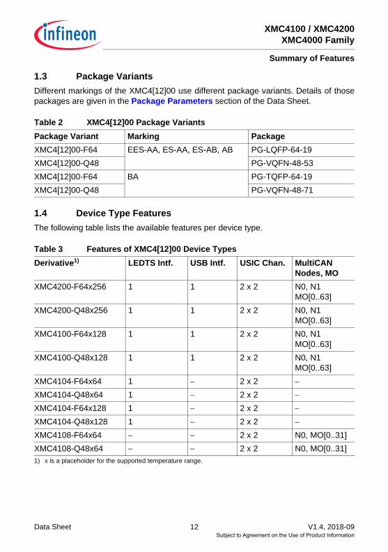
1.3 Package VariantsDifferent markings of the XMC4[12]00 use different package variants. Details of thosepackages are given in the Package Parameters section of the Data Sheet.
1.4 Device Type FeaturesThe following table lists the available features per device type.
Table 2 XMC4[12]00 Package VariantsPackage Variant Marking PackageXMC4[12]00-F64 EES-AA, ES-AA, ES-AB, AB PG-LQFP-64-19XMC4[12]00-Q48 PG-VQFN-48-53XMC4[12]00-F64 BA PG-TQFP-64-19XMC4[12]00-Q48 PG-VQFN-48-71
Table 3 Features of XMC4[12]00 Device TypesDerivative1)
1) x is a placeholder for the supported temperature range.
LEDTS Intf. USB Intf. USIC Chan. MultiCANNodes, MO
XMC4200-F64x256 1 1 2 x 2 N0, N1MO[0..63]
XMC4200-Q48x256 1 1 2 x 2 N0, N1MO[0..63]
XMC4100-F64x128 1 1 2 x 2 N0, N1MO[0..63]
XMC4100-Q48x128 1 1 2 x 2 N0, N1MO[0..63]
XMC4104-F64x64 1 − 2 x 2 −
XMC4104-Q48x64 1 − 2 x 2 −
XMC4104-F64x128 1 − 2 x 2 −
XMC4104-Q48x128 1 − 2 x 2 −
XMC4108-F64x64 − − 2 x 2 N0, MO[0..31]XMC4108-Q48x64 − − 2 x 2 N0, MO[0..31]
Subject to Agreement on the Use of Product Information

XMC4100 / XMC4200XMC4000 Family
Summary of Features
Data Sheet 13 V1.4, 2018-09
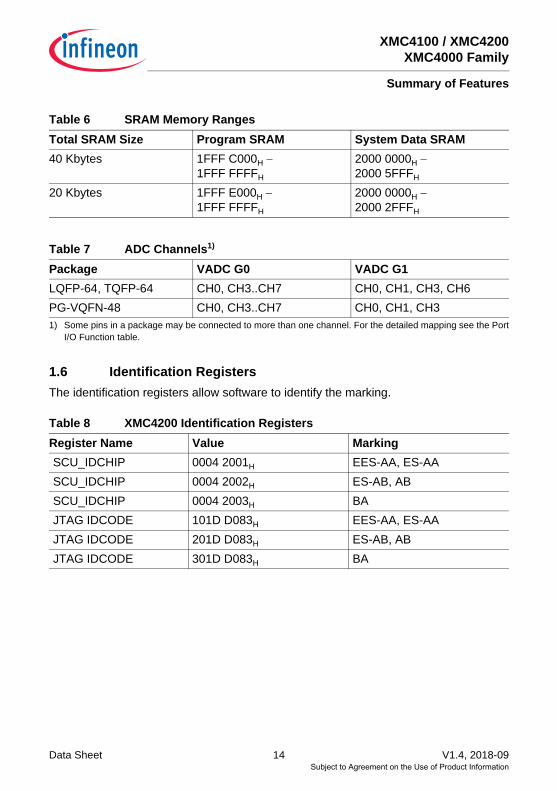
1.5 Definition of Feature VariantsThe XMC4[12]00 types are offered with several memory sizes and number of availableVADC channels. Table 5 describes the location of the available Flash memory, Table 6describes the location of the available SRAMs, Table 7 the available VADC channels.
Table 4 Features of XMC4[12]00 Device TypesDerivative1)
1) x is a placeholder for the supported temperature range.
ADC Chan.
DAC Chan.
CCU4 Slice
CCU8 Slice
POSIF Intf.
HRPWM Intf.
XMC4200-F64x256 10 2 2 x 4 1 x 4 1 1XMC4200-Q48x256 9 2 2 x 4 1 x 4 1 1XMC4100-F64x128 10 2 2 x 4 1 x 4 1 1XMC4100-Q48x128 9 2 2 x 4 1 x 4 1 1XMC4104-F64x64 10 2 2 x 4 1 x 4 1 1XMC4104-Q48x64 9 2 2 x 4 1 x 4 1 1XMC4104-F64x128 10 2 2 x 4 1 x 4 1 1XMC4104-Q48x128 9 2 2 x 4 1 x 4 1 1XMC4108-F64x64 10 2 2 x 4 1 x 4 1 −
XMC4108-Q48x64 9 2 2 x 4 1 x 4 1 −
Table 5 Flash Memory RangesTotal Flash Size Cached Range Uncached Range256 Kbytes 0800 0000H −
0803 FFFFH
0C00 0000H − 0C03 FFFFH
128 Kbytes 0800 0000H − 0801 FFFFH
0C00 0000H − 0C01 FFFFH
64 Kbytes 0800 0000H − 0800 FFFFH
0C00 0000H − 0C00 FFFFH
Subject to Agreement on the Use of Product Information
XMC4100 / XMC4200XMC4000 Family
Summary of Features
Data Sheet 14 V1.4, 2018-09
1.6 Identification RegistersThe identification registers allow software to identify the marking.
Table 6 SRAM Memory RangesTotal SRAM Size Program SRAM System Data SRAM40 Kbytes 1FFF C000H −
1FFF FFFFH
2000 0000H − 2000 5FFFH
20 Kbytes 1FFF E000H − 1FFF FFFFH
2000 0000H − 2000 2FFFH
Table 7 ADC Channels1)
1) Some pins in a package may be connected to more than one channel. For the detailed mapping see the PortI/O Function table.
Package VADC G0 VADC G1LQFP-64, TQFP-64 CH0, CH3..CH7 CH0, CH1, CH3, CH6PG-VQFN-48 CH0, CH3..CH7 CH0, CH1, CH3
Table 8 XMC4200 Identification RegistersRegister Name Value MarkingSCU_IDCHIP 0004 2001H EES-AA, ES-AASCU_IDCHIP 0004 2002H ES-AB, ABSCU_IDCHIP 0004 2003H BAJTAG IDCODE 101D D083H EES-AA, ES-AAJTAG IDCODE 201D D083H ES-AB, ABJTAG IDCODE 301D D083H BA
Subject to Agreement on the Use of Product Information
XMC4100 / XMC4200XMC4000 Family
Summary of Features
Data Sheet 15 V1.4, 2018-09
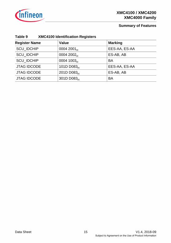
Table 9 XMC4100 Identification RegistersRegister Name Value MarkingSCU_IDCHIP 0004 2001H EES-AA, ES-AASCU_IDCHIP 0004 2002H ES-AB, ABSCU_IDCHIP 0004 1003H BAJTAG IDCODE 101D D083H EES-AA, ES-AAJTAG IDCODE 201D D083H ES-AB, ABJTAG IDCODE 301D D083H BA
Subject to Agreement on the Use of Product Information

XMC4100 / XMC4200XMC4000 Family
General Device Information
Data Sheet 16 V1.4, 2018-09
2 General Device InformationThis section summarizes the logic symbols and package pin configurations with adetailed list of the functional I/O mapping.
2.1 Logic Symbols
Figure 2 XMC4[12]00 Logic Symbol PG-LQFP-64 and PG-TQFP-64
Port 012 bit
Port 110 bit
Port 212 bit
VAGND
VSSA(1)
VAREF
VDDA(1)
VDDP(3)
JTAG3 bit
TCK SWD1 bit
VDDC(2)
XTAL1
XTAL2
USB_DP
USB_DM
Port 149 bit
TMS
PORST
via Port Pins
RTC_XTAL1
RTC_XTAL2
HIB_IO_0
VBAT (1)
(1) VSSO
Exp. Die Pad(VSS)
VSS(1)
Port 31 bit
Subject to Agreement on the Use of Product Information

XMC4100 / XMC4200XMC4000 Family
General Device Information
Data Sheet 17 V1.4, 2018-09
Figure 3 XMC4[12]00 Logic Symbol PG-VQFN-48
Port 09 bit
Port 16 bit
Port 26 bit
VAGND
VSSA(1)
VAREF
VDDA(1)
VDDP(3)
JTAG3 bit
TCK SWD1 bit
VDDC(2)
XTAL1
XTAL2
USB_DP
USB_DM
Port 148 bit
TMS
PORST
via Port Pins
RTC_XTAL1
RTC_XTAL2
HIB_IO_0
VBAT (1) Exp. Die Pad(VSS)
VSS(1)
Subject to Agreement on the Use of Product Information

XMC4100 / XMC4200XMC4000 Family
General Device Information
Data Sheet 18 V1.4, 2018-09
2.2 Pin Configuration and DefinitionThe following figures summarize all pins, showing their locations on the differentpackages.
Figure 4 XMC4[12]00 PG-LQFP-64 and PG-TQFP-64 Pin Configuration(top view)
2P0.01P0.1
64P
0.2
63P
0.3
62P
0.4
61P
0.5
60P
0.6
58P
0.7
57P
0.8
4P0.93P0.10
59P
0.11
52P
1.0
51P
1.1
50P
1.2
49P
1.3
48 P1.447 P1.5
55P
1.7
54P
1.8
53P
1.9
46 P1.15
34 P2.033 P2.1
32P2
.231
P2.3
30P2
.429
P2.5
36 P2.635 P2.7
28P2
.827
P2.9
26P
2.14
25P
2.15
5P3.0
20P
14.0
19P
14.3
18P
14.4
17P
14.5
16P14.615P14.7
24P
14.8
23P
14.9
14P14.14
10HIB_IO_0
43 PORST
11RTC_XTAL112RTC_XTAL2
45 TCK44 TMS
6USB_DM7USB_DP
13VBAT
22V
DD
A/VA
RE
F
9VDDC
42 VDDC8VDDP
38 VDDP
56V
DD
P
37 VSS
21VS
SA
/VA
GN
D
41 VSSO
39 XTAL140 XTAL2
XMC4[12]00(Top View)
Subject to Agreement on the Use of Product Information
XMC4100 / XMC4200XMC4000 Family
General Device Information
Data Sheet 19 V1.4, 2018-09
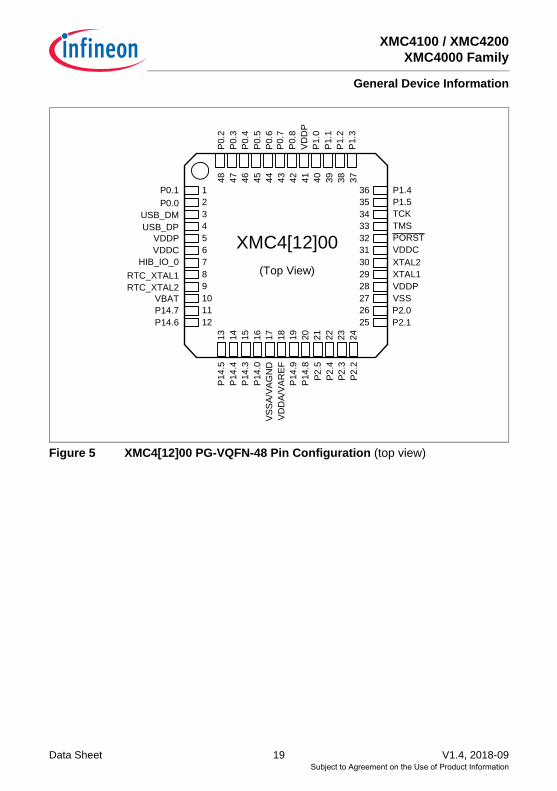
Figure 5 XMC4[12]00 PG-VQFN-48 Pin Configuration (top view)
2P0.01P0.1
48P
0.2
47P
0.3
46P
0.4
45P
0.5
44P
0.6
42P
0.7
41P
0.8
43
43
P1.
0P
1.1
P1.
2P
1.3
36 P1.435 P1.5
39 38 37
34
P2.0P2.1
P2.2
P2.3
P2.4
P2.5
24232221
5
16P
14.0
15P
14.3
14P
14.4
13P
14.5
P14.6P14.7
20P
14.8
19P
14.9
10
HIB_IO_031
PORST
11
RTC_XTAL1
12
RTC_XTAL2
33TCK
32TMS
6
USB_DM
7
USB_DP
VBAT
18V
DD
A/VA
RE
F9
VDDC30
VDDC
8
VDDP
26
VDDP
40V
DD
P
25
VSS
17VS
SA/
VAG
ND
29
27
XTAL128
XTAL2
XMC4[12]00(Top View)
Subject to Agreement on the Use of Product Information

XMC4100 / XMC4200XMC4000 Family
General Device Information
Data Sheet 20 V1.4, 2018-09
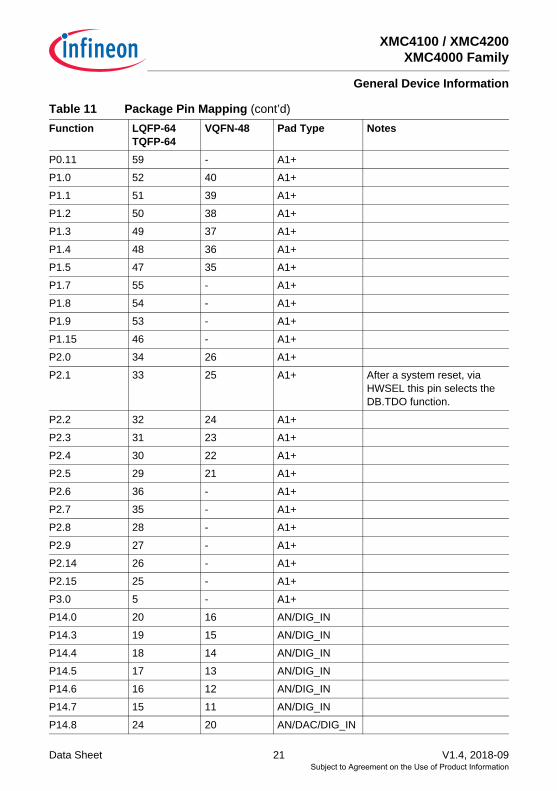
2.2.1 Package Pin SummaryThe following general scheme is used to describe each pin:
The table is sorted by the “Function” column, starting with the regular Port pins (Px.y),followed by the dedicated pins (i.e. PORST) and supply pins.The following columns, titled with the supported package variants, lists the package pinnumber to which the respective function is mapped in that package.The “Pad Type” indicates the employed pad type (A1, A1+, special=special pad,In=input pad, AN/DIG_IN=analog and digital input, Power=power supply). Details aboutthe pad properties are defined in the Electrical Parameters.In the “Notes”, special information to the respective pin/function is given, i.e. deviationsfrom the default configuration after reset. Per default the regular Port pins are configuredas direct input with no internal pull device active.
Table 10 Package Pin Mapping DescriptionFunction Package A Package B ... Pad
TypeNotes
Name N Ax ... A1+
Table 11 Package Pin MappingFunction LQFP-64
TQFP-64VQFN-48 Pad Type Notes
P0.0 2 2 A1+
P0.1 1 1 A1+
P0.2 64 48 A1+
P0.3 63 47 A1+
P0.4 62 46 A1+
P0.5 61 45 A1+
P0.6 60 44 A1+
P0.7 58 43 A1+ After a system reset, via HWSEL this pin selects the DB.TDI function.
P0.8 57 42 A1+ After a system reset, via HWSEL this pin selects the DB.TRST function, with a weak pull-down active.
P0.9 4 - A1+
P0.10 3 - A1+
Subject to Agreement on the Use of Product Information
XMC4100 / XMC4200XMC4000 Family
General Device Information
Data Sheet 21 V1.4, 2018-09
P0.11 59 - A1+
P1.0 52 40 A1+
P1.1 51 39 A1+
P1.2 50 38 A1+
P1.3 49 37 A1+
P1.4 48 36 A1+
P1.5 47 35 A1+
P1.7 55 - A1+
P1.8 54 - A1+
P1.9 53 - A1+
P1.15 46 - A1+
P2.0 34 26 A1+
P2.1 33 25 A1+ After a system reset, via HWSEL this pin selects the DB.TDO function.
P2.2 32 24 A1+
P2.3 31 23 A1+
P2.4 30 22 A1+
P2.5 29 21 A1+
P2.6 36 - A1+
P2.7 35 - A1+
P2.8 28 - A1+
P2.9 27 - A1+
P2.14 26 - A1+
P2.15 25 - A1+
P3.0 5 - A1+
P14.0 20 16 AN/DIG_IN
P14.3 19 15 AN/DIG_IN
P14.4 18 14 AN/DIG_IN
P14.5 17 13 AN/DIG_IN
P14.6 16 12 AN/DIG_IN
P14.7 15 11 AN/DIG_IN
P14.8 24 20 AN/DAC/DIG_IN
Table 11 Package Pin Mapping (cont’d)Function LQFP-64
TQFP-64VQFN-48 Pad Type Notes
Subject to Agreement on the Use of Product Information

XMC4100 / XMC4200XMC4000 Family
General Device Information
Data Sheet 22 V1.4, 2018-09
P14.9 23 19 AN/DAC/DIG_IN
P14.14 14 - AN/DIG_IN
USB_DP 7 4 special
USB_DM 6 3 special
HIB_IO_0 10 7 A1 special At the first power-up and with every reset of the hibernate domain this pin is configured as open-drain output and drives "0".As output the medium driver mode is active.
TCK 45 34 A1 Weak pull-down active.
TMS 44 33 A1+ Weak pull-up active.As output the strong-soft driver mode is active.
PORST 43 32 special Strong pull-down controlled by EVR. Weak pull-up active while strong pull-down is not active.
XTAL1 39 29 clock_IN
XTAL2 40 30 clock_O
RTC_XTAL1 11 8 clock_IN
RTC_XTAL2 12 9 clock_O
VBAT 13 10 Power When VDDP is supplied VBAT has to be supplied as well.
VDDA/VAREF 22 18 AN_Power/AN_Ref
Shared analog supply and reference voltage pin.
VSSA/VAGND 21 17 AN_Power/AN_Ref
Shared analog supply and reference ground pin.
VDDC 9 6 Power
VDDC 42 31 Power
VDDP 8 5 Power
VDDP 38 28 Power
VDDP 56 41 Power
VSS 37 27 Power
Table 11 Package Pin Mapping (cont’d)Function LQFP-64
TQFP-64VQFN-48 Pad Type Notes
Subject to Agreement on the Use of Product Information
XMC4100 / XMC4200XMC4000 Family
General Device Information
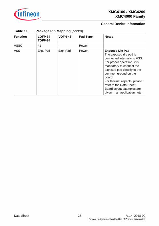
Data Sheet 23 V1.4, 2018-09
VSSO 41 - Power
VSS Exp. Pad Exp. Pad Power Exposed Die PadThe exposed die pad is connected internally to VSS. For proper operation, it is mandatory to connect the exposed pad directly to the common ground on the board.For thermal aspects, please refer to the Data Sheet. Board layout examples are given in an application note.
Table 11 Package Pin Mapping (cont’d)Function LQFP-64
TQFP-64VQFN-48 Pad Type Notes
Subject to Agreement on the Use of Product Information
XMC4100 / XMC4200XMC4000 Family
General Device Information
Data Sheet 24 V1.4, 2018-09
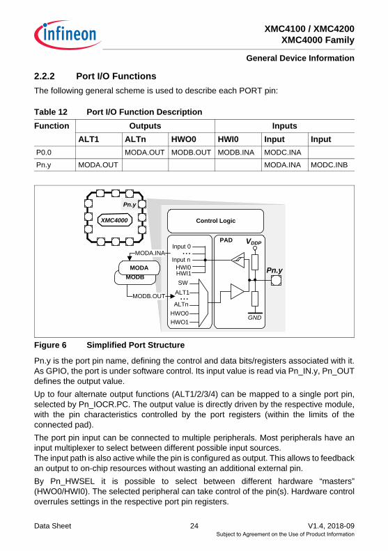
2.2.2 Port I/O FunctionsThe following general scheme is used to describe each PORT pin:
Figure 6 Simplified Port Structure
Pn.y is the port pin name, defining the control and data bits/registers associated with it.As GPIO, the port is under software control. Its input value is read via Pn_IN.y, Pn_OUTdefines the output value.Up to four alternate output functions (ALT1/2/3/4) can be mapped to a single port pin,selected by Pn_IOCR.PC. The output value is directly driven by the respective module,with the pin characteristics controlled by the port registers (within the limits of theconnected pad).The port pin input can be connected to multiple peripherals. Most peripherals have aninput multiplexer to select between different possible input sources.The input path is also active while the pin is configured as output. This allows to feedbackan output to on-chip resources without wasting an additional external pin.By Pn_HWSEL it is possible to select between different hardware “masters”(HWO0/HWI0). The selected peripheral can take control of the pin(s). Hardware controloverrules settings in the respective port pin registers.
Table 12 Port I/O Function DescriptionFunction Outputs Inputs
ALT1 ALTn HWO0 HWI0 Input Input P0.0 MODA.OUT MODB.OUT MODB.INA MODC.INA
Pn.y MODA.OUT MODA.INA MODC.INB
XMC4000
Pn.y
VDDP
GND
Pn.y
ALT1...ALTn
HWO0HWO1
SW
Control Logic
Input 0
Input n...
PAD
HWI0HWI1
MODB.OUT
MODBMODA
MODA.INA
Subject to Agreement on the Use of Product Information

XMC
4100 / XMC
4200XM
C4000 Fam
ily
Data S
heet25
V1.4, 2018-09
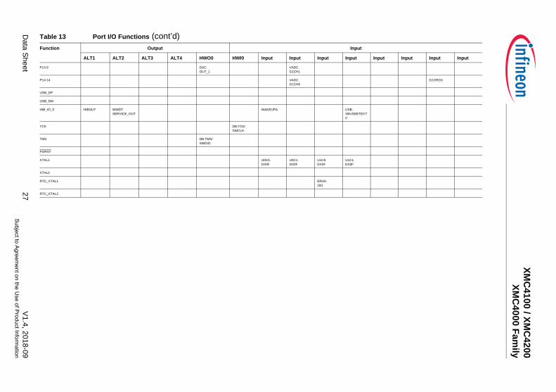
2.2.2.1 Port I/O Function Table
Table 13 Port I/O FunctionsFunction Output Input
ALT1 ALT2 ALT3 ALT4 HWO0 HWI0 Input Input Input Input Input Input Input Input
P0.0 CAN.N0_TXD
CCU80.OUT21
LEDTS0.COL2
U1C1.DX0D
ERU0.0B0
USB.VBUSDETECTA
HRPWM0.C1INB
P0.1 U1C1.DOUT0
CCU80.OUT11
LEDTS0.COL3
ERU0.0A0
HRPWM0.C2INB
P0.2 U1C1.SELO1
CCU80.OUT01
HRPWM0.HROUT01
U1C0.DOUT3
U1C0.HWIN3
ERU0.3B3
P0.3 CCU80.OUT20
HRPWM0.HROUT20
U1C0.DOUT2
U1C0.HWIN2
ERU1.3B0
P0.4 CCU80.OUT10
HRPWM0.HROUT21
U1C0.DOUT1
U1C0.HWIN1
U1C0.DX0A
ERU0.2B3
P0.5 U1C0.DOUT0
CCU80.OUT00
HRPWM0.HROUT00
U1C0.DOUT0
U1C0.HWIN0
U1C0.DX0B
ERU1.3A0
P0.6 U1C0.SELO0
CCU80.OUT30
HRPWM0.HROUT30
U1C0.DX2A
ERU0.3B2
CCU80.IN2B
P0.7 WWDT.SERVICE_OUT
U0C0.SELO0
HRPWM0.HROUT11
DB.TDI
U0C0.DX2B
ERU0.2B1
CCU80.IN0A
CCU80.IN1A
CCU80.IN2A
CCU80.IN3A
P0.8 SCU.EXTCLK
U0C0.SCLKOUT
HRPWM0.HROUT10
DB.TRST
U0C0.DX1B
ERU0.2A1
CCU80.IN1B
P0.9 HRPWM0.HROUT31
U1C1.SELO0
CCU80.OUT12
LEDTS0.COL0
U1C1.DX2A
ERU0.1B0
P0.10 U1C1.SCLKOUT
CCU80.OUT02
LEDTS0.COL1
U1C1.DX1A
ERU0.1A0
P0.11 U1C0.SCLKOUT
CCU80.OUT31
U1C0.DX1A
ERU0.3A2
P1.0 U0C0.SELO0
CCU40.OUT3
ERU1.PDOUT3
U0C0.DX2A
ERU0.3B0
CCU40.IN3A
HRPWM0.C0INA
P1.1 U0C0.SCLKOUT
CCU40.OUT2
ERU1.PDOUT2
U0C0.DX1A
POSIF0.IN2A
ERU0.3A0
CCU40.IN2A
HRPWM0.C1INA
P1.2 CCU40.OUT1
ERU1.PDOUT1
U0C0.DOUT3
U0C0.HWIN3
POSIF0.IN1A
ERU1.2B0
CCU40.IN1A
HRPWM0.C2INA
P1.3 U0C0.MCLKOUT
CCU40.OUT0
ERU1.PDOUT0
U0C0.DOUT2
U0C0.HWIN2
POSIF0.IN0A
ERU1.2A0
CCU40.IN0A
HRPWM0.C0INB
P1.4 WWDT.SERVICE_OUT
CAN.N0_TXD
CCU80.OUT33
U0C0.DOUT1
U0C0.HWIN1
U0C0.DX0B
CAN.N1_RXDD
ERU0.2B0
CCU41.IN0C
HRPWM0.BL0A
P1.5 CAN.N1_TXD
U0C0.DOUT0
CCU80.OUT23
U0C0.DOUT0
U0C0.HWIN0
U0C0.DX0A
CAN.N0_RXDA
ERU0.2A0
ERU1.0A0
CCU41.IN1C
P1.7 U0C0.DOUT0
U1C1.SELO2
USB.VBUSDETECTB
Subject to A
greement on the U
se of Product Inform
ation
XMC
4100 / XMC
4200XM
C4000 Fam
ily
Data S
heet26
V1.4, 2018-09
P1.8 U0C0.SELO1
U1C1.SCLKOUT
P1.9 U0C0.SCLKOUT
U1C1.DOUT0
P1.15 SCU.EXTCLK
U1C0.DOUT0
ERU1.1A0
P2.0 CAN.N0_TXD
LEDTS0.COL1
ERU0.0B3
CCU40.IN1C
P2.1 LEDTS0.COL0
DB.TDO/TRACESWO
ERU1.0B0
CCU40.IN0C
P2.2 VADC.EMUX00
CCU41.OUT3
LEDTS0.LINE0
LEDTS0.EXTENDED0
LEDTS0.TSIN0A
U0C1.DX0A
ERU0.1B2
CCU41.IN3A
P2.3 VADC.EMUX01
U0C1.SELO0
CCU41.OUT2
LEDTS0.LINE1
LEDTS0.EXTENDED1
LEDTS0.TSIN1A
U0C1.DX2A
ERU0.1A2
CCU41.IN2A
P2.4 VADC.EMUX02
U0C1.SCLKOUT
CCU41.OUT1
LEDTS0.LINE2
LEDTS0.EXTENDED2
LEDTS0.TSIN2A
U0C1.DX1A
ERU0.0B2
CCU41.IN1A
HRPWM0.BL1A
P2.5 U0C1.DOUT0
CCU41.OUT0
LEDTS0.LINE3
LEDTS0.EXTENDED3
LEDTS0.TSIN3A
U0C1.DX0B
ERU0.0A2
CCU41.IN0A
HRPWM0.BL2A
P2.6 CCU80.OUT13
LEDTS0.COL3
CAN.N1_RXDA
ERU0.1B3
CCU40.IN3C
P2.7 CAN.N1_TXD
CCU80.OUT03
LEDTS0.COL2
ERU1.1B0
CCU40.IN2C
P2.8 CCU80.OUT32
LEDTS0.LINE4
LEDTS0.EXTENDED4
LEDTS0.TSIN4A
DAC.TRIGGER5
CCU40.IN0B
CCU40.IN1B
CCU40.IN2B
CCU40.IN3B
P2.9 CCU80.OUT22
LEDTS0.LINE5
LEDTS0.EXTENDED5
LEDTS0.TSIN5A
DAC.TRIGGER4
CCU41.IN0B
CCU41.IN1B
CCU41.IN2B
CCU41.IN3B
P2.14 VADC.EMUX11
U1C0.DOUT0
CCU80.OUT21
U1C0.DX0D
P2.15 VADC.EMUX12
CCU80.OUT11
LEDTS0.LINE6
LEDTS0.EXTENDED6
LEDTS0.TSIN6A
U1C0.DX0C
P3.0 U0C1.SCLKOUT
U0C1.DX1B
CCU80.IN2C
P14.0 VADC.G0CH0
P14.3 VADC.G0CH3
VADC.G1CH3
CAN.N0_RXDB
P14.4 VADC.G0CH4
P14.5 VADC.G0CH5
POSIF0.IN2B
P14.6 VADC.G0CH6
POSIF0.IN1B
G0ORC6
P14.7 VADC.G0CH7
POSIF0.IN0B
P14.8 DAC.OUT_0
VADC.G1CH0
Table 13 Port I/O Functions (cont’d)Function Output Input
ALT1 ALT2 ALT3 ALT4 HWO0 HWI0 Input Input Input Input Input Input Input Input
Subject to A
greement on the U
se of Product Inform
ation
XMC
4100 / XMC
4200XM
C4000 Fam
ily
Data S
heet27
V1.4, 2018-09
P14.9 DAC.OUT_1
VADC.G1CH1
P14.14 VADC.G1CH6
G1ORC6
USB_DP
USB_DM
HIB_IO_0 HIBOUT WWDT.SERVICE_OUT
WAKEUPA USB.VBUSDETECTC
TCK DB.TCK/SWCLK
TMS DB.TMS/SWDIO
PORST
XTAL1 U0C0.DX0F
U0C1.DX0F
U1C0.DX0F
U1C1.DX0F
XTAL2
RTC_XTAL1 ERU0.1B1
RTC_XTAL2
Table 13 Port I/O Functions (cont’d)Function Output Input
ALT1 ALT2 ALT3 ALT4 HWO0 HWI0 Input Input Input Input Input Input Input Input
Subject to A
greement on the U
se of Product Inform
ation

XMC4100 / XMC4200XMC4000 Family
Data Sheet 28 V1.4, 2018-09
2.3 Power Connection SchemeFigure 7. shows a reference power connection scheme for the XMC4[12]00.
Figure 7 Power Connection Scheme
Every power supply pin needs to be connected. Different pins of the same supply needalso to be externally connected. As example, all VDDP pins must be connected externallyto one VDDP net. In this reference scheme one 100 nF capacitor is connected at eachsupply pin against VSS. An additional 10 µF capacitor is connected to the VDDP nets andan additional 4.7uF capacitor to the VDDC nets.
VBAT
M x VDDC
N x VDDP
VSS
VDDA / VAREF
Hibernate domain
RTC Hibernate control
Retention Memory
32 kHz Clock
Core Domain
CPUDig. Peripherals
Analog Domain
ADC DAC
GPIOs
Out-of-range comparator
PAD Domain
Level shift.
FLASH
RAMs
100 nF x M
4.7 µF x 1
100 nF
3.3V
XMC4000
EVR
VSSA / VAGND
Exp. Die Pad VSS
GND
GND
GND
GND
100 nF x N
10 µF x 1
3.3V
2.1...3.6 V
Subject to Agreement on the Use of Product Information
XMC4100 / XMC4200XMC4000 Family
Data Sheet 29 V1.4, 2018-09
The XMC4[12]00 has a common ground concept, all VSS, VSSA and VSSO pins share thesame ground potential. In packages with an exposed die pad it must be connected to thecommon ground as well.There are no dedicated connections for the analog reference VAREF and VAGND. Instead,they share the same pins as the analog supply pins VDDA and VSSA.Some analogchannels can optionally serve as “Alternate Reference”; further details on this operatingmode are described in the Reference Manual.When VDDP is supplied, VBAT must be supplied as well. If no other supply source (e.g.battery) is connected to VBAT, the VBAT pin can also be connected directly to VDDP.
Subject to Agreement on the Use of Product Information
XMC4100 / XMC4200XMC4000 Family
Electrical Parameters
Data Sheet 30 V1.4, 2018-09
3 Electrical Parameters
3.1 General Parameters
3.1.1 Parameter InterpretationThe parameters listed in this section partly represent the characteristics of theXMC4[12]00 and partly its requirements on the system. To aid interpreting theparameters easily when evaluating them for a design, they are marked with an two-letterabbreviation in column “Symbol”:• CC
Such parameters indicate Controller Characteristics, which are a distinctive featureof the XMC4[12]00 and must be regarded for system design.
• SRSuch parameters indicate System Requirements, which must be provided by theapplication system in which the XMC4[12]00 is designed in.
Subject to Agreement on the Use of Product Information

XMC4100 / XMC4200XMC4000 Family
Electrical Parameters
Data Sheet 31 V1.4, 2018-09
3.1.2 Absolute Maximum RatingsStresses above the values listed under “Absolute Maximum Ratings” may causepermanent damage to the device. This is a stress rating only and functional operation ofthe device at these or any other conditions above those indicated in the operationalsections of this specification is not implied. Exposure to absolute maximum ratingconditions may affect device reliability.
Table 14 Absolute Maximum Rating ParametersParameter Symbol Values Unit Note /
Test Condition
Min. Typ. Max.
Storage temperature TST SR -65 – 150 °C –Junction temperature TJ SR -40 − 150 °C –Voltage at 3.3 V power supply pins with respect to VSS
VDDP SR – – 4.3 V –
Voltage on any Class A and dedicated input pin with respect to VSS
VIN SR -1.0 – VDDP + 1.0or max. 4.3
V whichever is lower
Voltage on any analog input pin with respect to VAGND
VAINVAREF SR
-1.0 – VDDP + 1.0or max. 4.3
V whichever is lower
Input current on any pin during overload condition
IIN SR -10 – +10 mA
Absolute maximum sum of all input circuit currents for one port group during overload condition1)
1) The port groups are defined in Table 18.
ΣIIN SR -25 – +25 mA
Absolute maximum sum of all input circuit currents during overload condition
ΣIIN SR -100 – +100 mA
Subject to Agreement on the Use of Product Information

XMC4100 / XMC4200XMC4000 Family
Electrical Parameters
Data Sheet 32 V1.4, 2018-09
Figure 8 explains the input voltage ranges of VIN and VAIN and its dependency to thesupply level of VDDP.The input voltage must not exceed 4.3 V, and it must not be morethan 1.0 V above VDDP. For the range up to VDDP + 1.0 V also see the definition of theoverload conditions in Section 3.1.3.
Figure 8 Absolute Maximum Input Voltage Ranges
V
4.3
VSS
-1.0
A
A
B
Abs. max. input voltage VIN with VDDP > 3.3 V
Abs. max. input voltage VIN with VDDP ≤ 3.3 V
V
VDDP + 1.0
VSS
-1.0
VDDP
B
Subject to Agreement on the Use of Product Information

XMC4100 / XMC4200XMC4000 Family
Electrical Parameters
Data Sheet 33 V1.4, 2018-09
3.1.3 Pin Reliability in OverloadWhen receiving signals from higher voltage devices, low-voltage devices experienceoverload currents and voltages that go beyond their own IO power supplies specification.Table 15 defines overload conditions that will not cause any negative reliability impact ifall the following conditions are met:• full operation life-time is not exceeded• Operating Conditions are met for
– pad supply levels (VDDP or VDDA)– temperature
If a pin current is outside of the Operating Conditions but within the overloadparameters, then the parameters functionality of this pin as stated in the OperatingConditions can no longer be guaranteed. Operation is still possible in most cases butwith relaxed parameters.Note: An overload condition on one or more pins does not require a reset.
Note: A series resistor at the pin to limit the current to the maximum permitted overloadcurrent is sufficient to handle failure situations like short to battery.
Figure 9 shows the path of the input currents during overload via the ESD protectionstructures. The diodes against VDDP and ground are a simplified representation of theseESD protection structures.
Table 15 Overload ParametersParameter Symbol Values Unit Note /
Test ConditionMin. Typ. Max.Input current on any port pin during overload condition
IOV SR -5 – 5 mA
Absolute sum of all input circuit currents for one port group during overload condition1)
1) The port groups are defined in Table 18.
IOVG SR – – 20 mA Σ|IOVx|, for all IOVx < 0 mA
– – 20 mA Σ|IOVx|, for all IOVx > 0 mA
Absolute sum of all input circuit currents during overload condition
IOVS SR – – 80 mA ΣIOVG
Subject to Agreement on the Use of Product Information

XMC4100 / XMC4200XMC4000 Family
Electrical Parameters
Data Sheet 34 V1.4, 2018-09
Figure 9 Input Overload Current via ESD structures
Table 16 and Table 17 list input voltages that can be reached under overload conditions.Note that the absolute maximum input voltages as defined in the Absolute MaximumRatings must not be exceeded during overload.
Table 16 PN-Junction Characterisitics for positive OverloadPad Type IOV = 5 mA, TJ = -40 °C IOV = 5 mA, TJ = 150 °CA1 / A1+ VIN = VDDP + 1.0 V VIN = VDDP + 0.75 VAN/DIG_IN VIN = VDDP + 1.0 V VIN = VDDP + 0.75 V
Table 17 PN-Junction Characterisitics for negative OverloadPad Type IOV = 5 mA, TJ = -40 °C IOV = 5 mA, TJ = 150 °CA1 / A1+ VIN = VSS - 1.0 V VIN = VSS - 0.75 VAN/DIG_IN VIN = VDDP - 1.0 V VIN = VDDP - 0.75 V
Table 18 Port Groups for Overload and Short-Circuit Current Sum Parameters
Group Pins1 P0.[12:0], P3.02 P14.[8:0]3 P2.[15:0]4 P1.[15:0]
Pn.y IOVx
GNDESD Pad
GND
VDDPVDDP
Subject to Agreement on the Use of Product Information
XMC4100 / XMC4200XMC4000 Family
Electrical Parameters
Data Sheet 35 V1.4, 2018-09
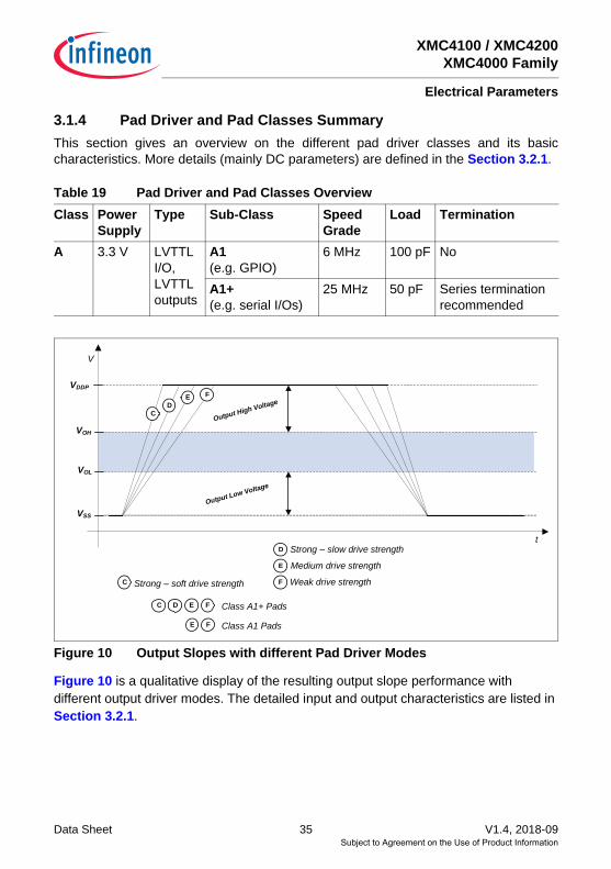
3.1.4 Pad Driver and Pad Classes SummaryThis section gives an overview on the different pad driver classes and its basiccharacteristics. More details (mainly DC parameters) are defined in the Section 3.2.1.
Figure 10 Output Slopes with different Pad Driver Modes
Figure 10 is a qualitative display of the resulting output slope performance with different output driver modes. The detailed input and output characteristics are listed in Section 3.2.1.
Table 19 Pad Driver and Pad Classes OverviewClass Power
SupplyType Sub-Class Speed
GradeLoad Termination
A 3.3 V LVTTL I/O, LVTTL outputs
A1(e.g. GPIO)
6 MHz 100 pF No
A1+(e.g. serial I/Os)
25 MHz 50 pF Series termination recommended
V
VDDP
VSS
VOH
VOL
t
CD
E F
C
D
E
F
Output High Voltage
Output Low Voltage
Weak drive strength
Medium drive strength
Strong – slow drive strength
Strong – soft drive strength
C D E F Class A1+ Pads
E F Class A1 Pads
Subject to Agreement on the Use of Product Information
XMC4100 / XMC4200XMC4000 Family
Electrical Parameters
Data Sheet 36 V1.4, 2018-09
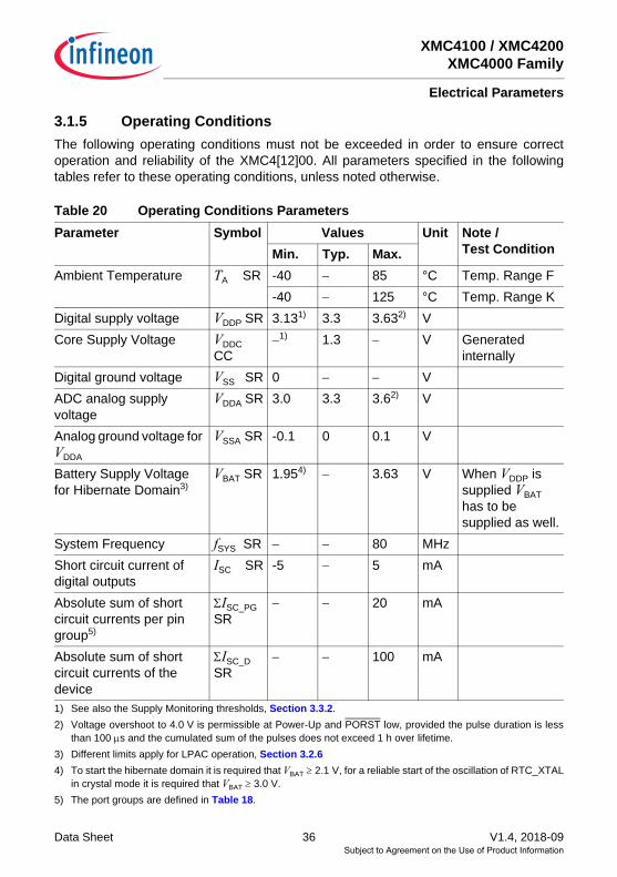
3.1.5 Operating ConditionsThe following operating conditions must not be exceeded in order to ensure correctoperation and reliability of the XMC4[12]00. All parameters specified in the followingtables refer to these operating conditions, unless noted otherwise.
Table 20 Operating Conditions ParametersParameter Symbol Values Unit Note /
Test ConditionMin. Typ. Max.Ambient Temperature TA SR -40 − 85 °C Temp. Range F
-40 − 125 °C Temp. Range KDigital supply voltage VDDP SR 3.131)
1) See also the Supply Monitoring thresholds, Section 3.3.2.
3.3 3.632)
2) Voltage overshoot to 4.0 V is permissible at Power-Up and PORST low, provided the pulse duration is lessthan 100 μs and the cumulated sum of the pulses does not exceed 1 h over lifetime.
VCore Supply Voltage VDDC
CC−1) 1.3 − V Generated
internallyDigital ground voltage VSS SR 0 − − VADC analog supply voltage
VDDA SR 3.0 3.3 3.62) V
Analog ground voltage for VDDA
VSSA SR -0.1 0 0.1 V
Battery Supply Voltage for Hibernate Domain3)
3) Different limits apply for LPAC operation, Section 3.2.6
VBAT SR 1.954)
4) To start the hibernate domain it is required that VBAT ≥ 2.1 V, for a reliable start of the oscillation of RTC_XTALin crystal mode it is required that VBAT ≥ 3.0 V.
− 3.63 V When VDDP is supplied VBAT has to be supplied as well.
System Frequency fSYS SR − − 80 MHzShort circuit current of digital outputs
ISC SR -5 − 5 mA
Absolute sum of short circuit currents per pin group5)
5) The port groups are defined in Table 18.
ΣISC_PG SR
− − 20 mA
Absolute sum of short circuit currents of the device
ΣISC_D SR
− − 100 mA
Subject to Agreement on the Use of Product Information
XMC4100 / XMC4200XMC4000 Family
Electrical Parameters
Data Sheet 37 V1.4, 2018-09
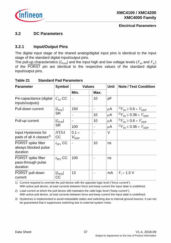
3.2 DC Parameters
3.2.1 Input/Output PinsThe digital input stage of the shared analog/digital input pins is identical to the inputstage of the standard digital input/output pins.The pull-up characteristics (IPUH) and the input high and low voltage levels (VIH and VIL)of the PORST pin are identical to the respective values of the standard digitalinput/output pins.
Table 21 Standard Pad ParametersParameter Symbol Values Unit Note / Test Condition
Min. Max.Pin capacitance (digital inputs/outputs)
CIO CC − 10 pF
Pull-down current |IPDL| SR
150 − μA 1)VIN ≥ 0.6 × VDDP
1) Current required to override the pull device with the opposite logic level (“force current”).With active pull device, at load currents between force and keep current the input state is undefined.
− 10 μA 2)VIN ≤ 0.36 × VDDP
2) Load current at which the pull device still maintains the valid logic level (“keep current”).With active pull device, at load currents between force and keep current the input state is undefined.
Pull-up current |IPUH| SR
− 10 μA 2)VIN ≥ 0.6 × VDDP
100 − μA 1)VIN ≤ 0.36 × VDDP
Input Hysteresis for pads of all A classes3)
3) Hysteresis is implemented to avoid metastable states and switching due to internal ground bounce. It can notbe guaranteed that it suppresses switching due to external system noise.
HYSA CC
0.1 × VDDP
− V
PORST spike filter always blocked pulse duration
tSF1 CC − 10 ns
PORST spike filter pass-through pulse duration
tSF2 CC 100 − ns
PORST pull-down current
|IPPD| CC
13 − mA Vi = 1.0 V
Subject to Agreement on the Use of Product Information
XMC4100 / XMC4200XMC4000 Family
Electrical Parameters
Data Sheet 38 V1.4, 2018-09
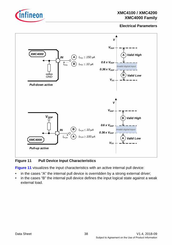
Figure 11 Pull Device Input Characteristics
Figure 11 visualizes the input characteristics with an active internal pull device:• in the cases “A” the internal pull device is overridden by a strong external driver;• in the cases “B” the internal pull device defines the input logical state against a weak
external load.
XMC4000IN
IPDL
A IPDL ≥ 150 μA
B IPDL ≤ 10 μA
VDDP
GND
V
VDDP
VSS
0.6 x VDDP
A
0.36 x VDDP
B
Valid High
Valid Low
Invalid digital input
XMC4000
IN
IPUH A IPUH ≥ 100 μA
B IPUH ≤ 10 μA
V
VDDP
VSS
0.6 x VDDP
B
0.36 x VDDP
A
Valid High
Valid Low
Invalid digital input
Pull-down active
Pull-up active
Subject to Agreement on the Use of Product Information
XMC4100 / XMC4200XMC4000 Family
Electrical Parameters
Data Sheet 39 V1.4, 2018-09
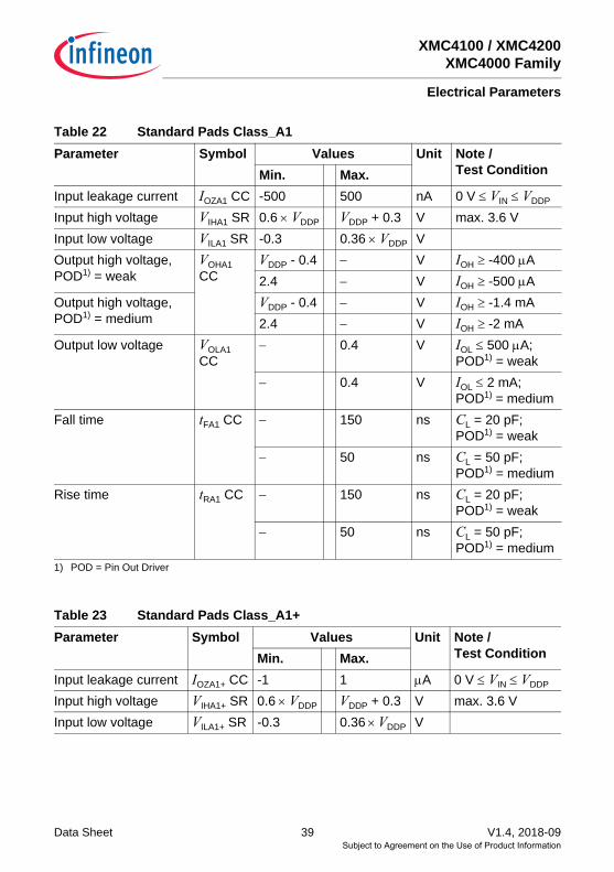
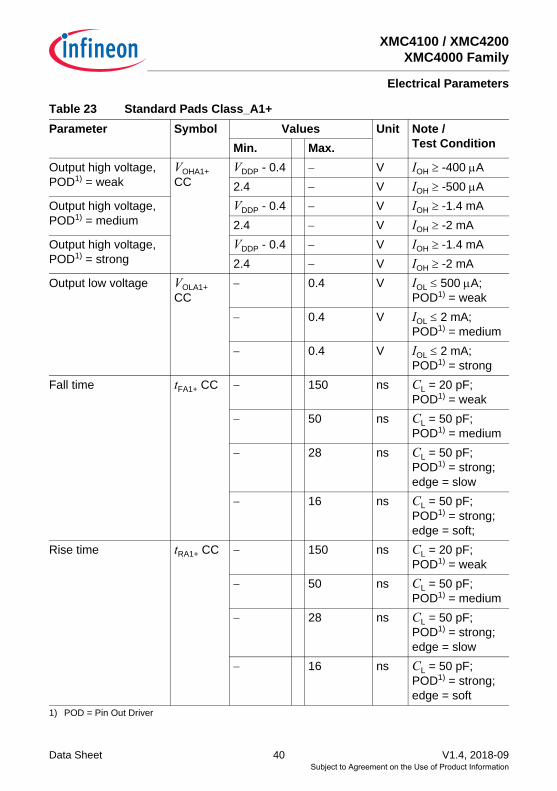
Table 22 Standard Pads Class_A1Parameter Symbol Values Unit Note /
Test ConditionMin. Max.Input leakage current IOZA1 CC -500 500 nA 0 V ≤ VIN ≤ VDDP
Input high voltage VIHA1 SR 0.6 × VDDP VDDP + 0.3 V max. 3.6 VInput low voltage VILA1 SR -0.3 0.36 × VDDP VOutput high voltage, POD1) = weak
VOHA1CC
VDDP - 0.4 − V IOH ≥ -400 μA2.4 − V IOH ≥ -500 μA
Output high voltage, POD1) = medium
VDDP - 0.4 − V IOH ≥ -1.4 mA2.4 − V IOH ≥ -2 mA
Output low voltage VOLA1CC
− 0.4 V IOL ≤ 500 μA;POD1) = weak
− 0.4 V IOL ≤ 2 mA;POD1) = medium
Fall time tFA1 CC − 150 ns CL = 20 pF;POD1) = weak
1) POD = Pin Out Driver
− 50 ns CL = 50 pF;POD1) = medium
Rise time tRA1 CC − 150 ns CL = 20 pF;POD1) = weak
− 50 ns CL = 50 pF;POD1) = medium
Table 23 Standard Pads Class_A1+Parameter Symbol Values Unit Note /
Test ConditionMin. Max.Input leakage current IOZA1+ CC -1 1 μA 0 V ≤ VIN ≤ VDDP
Input high voltage VIHA1+ SR 0.6 × VDDP VDDP + 0.3 V max. 3.6 VInput low voltage VILA1+ SR -0.3 0.36 × VDDP V
Subject to Agreement on the Use of Product Information
XMC4100 / XMC4200XMC4000 Family
Electrical Parameters
Data Sheet 40 V1.4, 2018-09
Output high voltage, POD1) = weak
VOHA1+ CC
VDDP - 0.4 − V IOH ≥ -400 μA2.4 − V IOH ≥ -500 μA
Output high voltage,POD1) = medium
VDDP - 0.4 − V IOH ≥ -1.4 mA2.4 − V IOH ≥ -2 mA
Output high voltage,POD1) = strong
VDDP - 0.4 − V IOH ≥ -1.4 mA2.4 − V IOH ≥ -2 mA
Output low voltage VOLA1+ CC
− 0.4 V IOL ≤ 500 μA;POD1) = weak
− 0.4 V IOL ≤ 2 mA;POD1) = medium
− 0.4 V IOL ≤ 2 mA;POD1) = strong
Fall time tFA1+ CC − 150 ns CL = 20 pF;POD1) = weak
− 50 ns CL = 50 pF;POD1) = medium
− 28 ns CL = 50 pF;POD1) = strong;edge = slow
− 16 ns CL = 50 pF;POD1) = strong;edge = soft;
Rise time tRA1+ CC − 150 ns CL = 20 pF;POD1) = weak
− 50 ns CL = 50 pF;POD1) = medium
− 28 ns CL = 50 pF;POD1) = strong;edge = slow
− 16 ns CL = 50 pF;POD1) = strong;edge = soft
1) POD = Pin Out Driver
Table 23 Standard Pads Class_A1+Parameter Symbol Values Unit Note /
Test ConditionMin. Max.
Subject to Agreement on the Use of Product Information
XMC4100 / XMC4200XMC4000 Family
Electrical Parameters
Data Sheet 41 V1.4, 2018-09
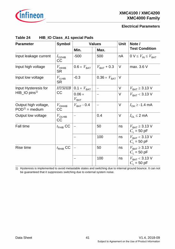
Table 24 HIB_IO Class_A1 special PadsParameter Symbol Values Unit Note /
Test ConditionMin. Max.Input leakage current IOZHIB
CC-500 500 nA 0 V ≤ VIN ≤ VBAT
Input high voltage VIHHIBSR
0.6 × VBAT VBAT + 0.3 V max. 3.6 V
Input low voltage VILHIBSR
-0.3 0.36 × VBAT V
Input Hysteresis for HIB_IO pins1)
1) Hysteresis is implemented to avoid metastable states and switching due to internal ground bounce. It can notbe guaranteed that it suppresses switching due to external system noise.
HYSHIB CC
0.1 × VBAT − V VBAT ≥ 3.13 V0.06 × VBAT
− V VBAT < 3.13 V
Output high voltage, POD1) = medium
VOHHIBCC
VBAT - 0.4 − V IOH ≥ -1.4 mA
Output low voltage VOLHIBCC
− 0.4 V IOL ≤ 2 mA
Fall time tFHIB CC − 50 ns VBAT ≥ 3.13 VCL = 50 pF
− 100 ns VBAT < 3.13 VCL = 50 pF
Rise time tRHIB CC − 50 ns VBAT ≥ 3.13 VCL = 50 pF
− 100 ns VBAT < 3.13 VCL = 50 pF
Subject to Agreement on the Use of Product Information

XMC4100 / XMC4200XMC4000 Family
Electrical Parameters
Data Sheet 42 V1.4, 2018-09
3.2.2 Analog to Digital Converters (ADCx)
Table 25 ADC Parameters (Operating Conditions apply)
Parameter Symbol Values Unit Note / Test ConditionMin. Typ. Max.
Analog reference voltage VAREF SR
− − − V VAREF = VDDAshared analog supply and reference input pin
Alternate reference voltage5)
VAREF SR
VAGND + 1
− VDDA + 0.051)
V
Analog reference ground VAGND SR
− − − V VAGND = VSSAshared analog supply and reference input pin
Alternate reference voltage range2)5)
VAREF - VAGND SR
1 − VDDA + 0.1
V
Analog input voltage VAIN SR VAGND − VDDA VInput leakage at analog inputs3)
IOZ1 CC -100 − 200 nA 0.03 × VDDA < VAIN < 0.97 × VDDA
-500 − 100 nA 0 V ≤ VAIN ≤ 0.03 × VDDA
-100 − 500 nA 0.97 × VDDA ≤ VAIN ≤ VDDA
Internal ADC clock fADCI CC 2 − 30 MHz VDDA = 3.3 VSwitched capacitance at the analog voltage inputs4)
CAINSW CC
− 4 6.5 pF
Total capacitance of an analog input
CAINTOT CC
− 12 20 pF
Switched capacitance at the alternate reference voltage input5)6)
CAREFSW CC
− 15 30 pF
Subject to Agreement on the Use of Product Information

XMC4100 / XMC4200XMC4000 Family
Electrical Parameters
Data Sheet 43 V1.4, 2018-09
Total capacitance of the alternate reference inputs5)
CAREFTOT CC
− 20 40 pF
Total Unadjusted Error TUE CC -6 − 6 LSB 12-bit resolution; VDDA = 3.3 V;VAREF = VDDA
7)Differential Non-Linearity Error8)
EADNL CC
-4.5 − 4.5 LSB
Gain Error8) EAGAIN CC
-6 − 6 LSB
Integral Non-Linearity8) EAINLCC -4.5 − 4.5 LSBOffset Error8) EAOFF
CC-6 − 6 LSB
RMS Noise9) ENRMS CC
− 1 210)11) LSB
Worst case ADC VDDA power supply current per active converter
IDDAACC
− 1.5 2 mA during conversionVDDP = 3.6 V,TJ = 150 oC
Charge consumption on alternate reference per conversion5)
QCONV CC
− 30 − pC 0 V ≤ VAREF ≤ VDDA
12)
ON resistance of the analog input path
RAIN CC − 600 1 200 Ohm
ON resistance for the ADC test (pull down for AIN7)
RAIN7T CC
180 550 900 Ohm
1) A running conversion may become imprecise in case the normal conditions are violated (voltage overshoot).2) If the analog reference voltage is below VDDA, then the ADC converter errors increase. If the reference voltage
is reduced by the factor k (k<1), TUE, DNL, INL, Gain, and Offset errors increase also by the factor 1/k.3) The leakage current definition is a continuous function, as shown in figure ADCx Analog Inputs Leakage. The
numerical values defined determine the characteristic points of the given continuous linear approximation -they do not define step function (see Figure 14).
4) The sampling capacity of the conversion C-network is pre-charged to VAREF/2 before the sampling moment.Because of the parasitic elements, the voltage measured at AINx can deviate from VAREF/2.
5) Applies to AINx, when used as alternate reference input.6) This represents an equivalent switched capacitance. This capacitance is not switched to the reference voltage
at once. Instead, smaller capacitances are successively switched to the reference voltage.7) For 10-bit conversions, the errors are reduced to 1/4; for 8-bit conversions, the errors are reduced to 1/16.
Never less than ±1 LSB.
Table 25 ADC Parameters (Operating Conditions apply)
Parameter Symbol Values Unit Note / Test ConditionMin. Typ. Max.
Subject to Agreement on the Use of Product Information

XMC4100 / XMC4200XMC4000 Family
Electrical Parameters
Data Sheet 44 V1.4, 2018-09
Figure 12 VADC Reference Voltage Range
8) The sum of DNL/INL/GAIN/OFF errors does not exceed the related total unadjusted error TUE.9) This parameter is valid for soldered devices and requires careful analog board design.10) Resulting worst case combined error is arithmetic combination of TUE and ENRMS.
11) Value is defined for one sigma Gauss distribution.12) The resulting current for a conversion can be calculated with IAREF = QCONV / tc.
The fastest 12-bit post-calibrated conversion of tc = 566 ns results in a typical average current ofIAREF = 53 µA.
Minimum VAREF - VAGND is 1 V
V
VDDA + 0.05
VAGND + 1
VAGND
Valid VAREF
VDDA
e.g. VAREF = 4/5 of VDDA
Conversion error increases by 5/4
Precise conversion range (12 bit)
t
V AR
EF
VSSA
Subject to Agreement on the Use of Product Information

XMC4100 / XMC4200XMC4000 Family
Electrical Parameters
Data Sheet 45 V1.4, 2018-09
The power-up calibration of the ADC requires a maximum number of 4 352 fADCI cycles.
Figure 13 ADCx Input Circuits
Figure 14 ADCx Analog Input Leakage Current
Reference Voltage Input Circuitry
Analog Input Circuitry
Analog_InpRefDiag
REXT
=VAIN CEXT
RAIN, On
CAINTOT - CAINSW
CAINSW
ANx
VAREF
RAREF, On
CAREFTOT - CAREFSW CAREFSW
VAGNDx
VAREFx
RAIN7TVAGNDx
ADC-Leakage.vsd
VIN [% VDDA]
200 nA
500 nA
3% 100%97%
IOZ1
100 nA
-500 nA
-100 nA
Single ADC Input
Subject to Agreement on the Use of Product Information
XMC4100 / XMC4200XMC4000 Family
Electrical Parameters
Data Sheet 46 V1.4, 2018-09
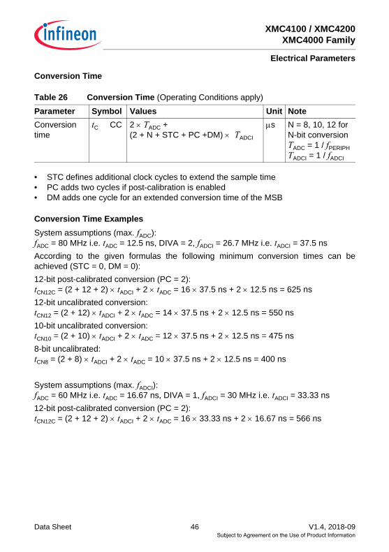
Conversion Time
• STC defines additional clock cycles to extend the sample time• PC adds two cycles if post-calibration is enabled• DM adds one cycle for an extended conversion time of the MSB
Conversion Time ExamplesSystem assumptions (max. fADC):fADC = 80 MHz i.e. tADC = 12.5 ns, DIVA = 2, fADCI = 26.7 MHz i.e. tADCI = 37.5 nsAccording to the given formulas the following minimum conversion times can beachieved (STC = 0, DM = 0):12-bit post-calibrated conversion (PC = 2):tCN12C = (2 + 12 + 2) × tADCI + 2 × tADC = 16 × 37.5 ns + 2 × 12.5 ns = 625 ns12-bit uncalibrated conversion:tCN12 = (2 + 12) × tADCI + 2 × tADC = 14 × 37.5 ns + 2 × 12.5 ns = 550 ns10-bit uncalibrated conversion:tCN10 = (2 + 10) × tADCI + 2 × tADC = 12 × 37.5 ns + 2 × 12.5 ns = 475 ns8-bit uncalibrated:tCN8 = (2 + 8) × tADCI + 2 × tADC = 10 × 37.5 ns + 2 × 12.5 ns = 400 ns
System assumptions (max. fADCI):fADC = 60 MHz i.e. tADC = 16.67 ns, DIVA = 1, fADCI = 30 MHz i.e. tADCI = 33.33 ns12-bit post-calibrated conversion (PC = 2):tCN12C = (2 + 12 + 2) × tADCI + 2 × tADC = 16 × 33.33 ns + 2 × 16.67 ns = 566 ns
Table 26 Conversion Time (Operating Conditions apply)
Parameter Symbol Values Unit NoteConversion time
tC CC 2 × TADC +(2 + N + STC + PC +DM) × TADCI
μs N = 8, 10, 12 for N-bit conversionTADC = 1 / fPERIPHTADCI = 1 / fADCI
Subject to Agreement on the Use of Product Information
XMC4100 / XMC4200XMC4000 Family
Electrical Parameters
Data Sheet 47 V1.4, 2018-09
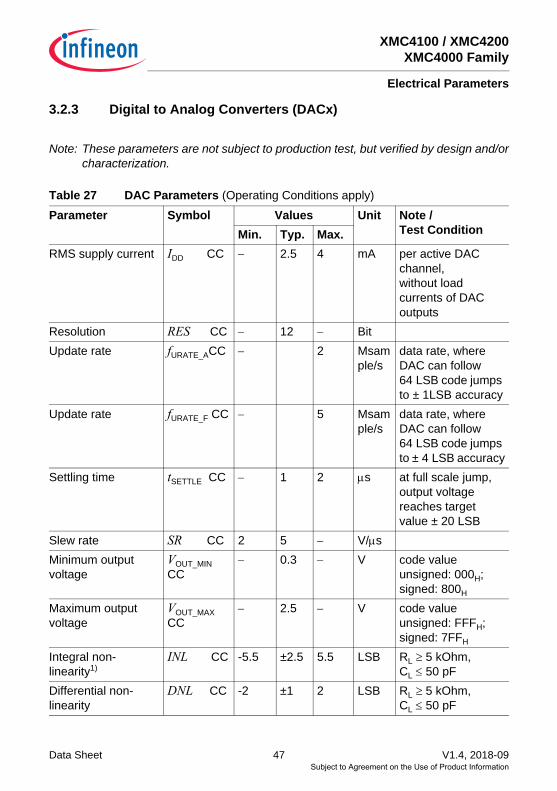
3.2.3 Digital to Analog Converters (DACx)
Note: These parameters are not subject to production test, but verified by design and/orcharacterization.
Table 27 DAC Parameters (Operating Conditions apply)
Parameter Symbol Values Unit Note / Test ConditionMin. Typ. Max.
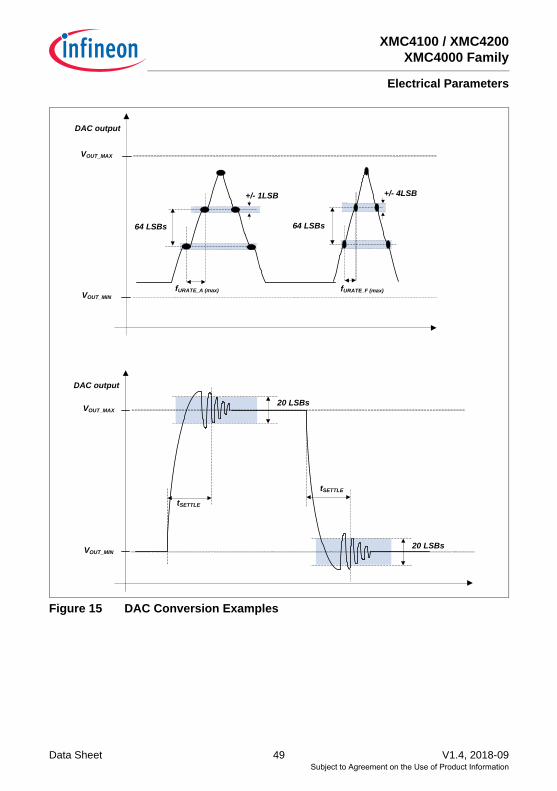
RMS supply current IDD CC − 2.5 4 mA per active DAC channel,without load currents of DAC outputs
Resolution RES CC − 12 − BitUpdate rate fURATE_ACC − 2 Msam
ple/sdata rate, where DAC can follow 64 LSB code jumps to ± 1LSB accuracy
Update rate fURATE_F CC − 5 Msample/s
data rate, where DAC can follow 64 LSB code jumps to ± 4 LSB accuracy
Settling time tSETTLE CC − 1 2 μs at full scale jump, output voltage reaches target value ± 20 LSB
Slew rate SR CC 2 5 − V/μsMinimum output voltage
VOUT_MIN CC
− 0.3 − V code value unsigned: 000H;signed: 800H
Maximum output voltage
VOUT_MAX CC
− 2.5 − V code value unsigned: FFFH;signed: 7FFH
Integral non-linearity1)
INL CC -5.5 ±2.5 5.5 LSB RL ≥ 5 kOhm,CL ≤ 50 pF
Differential non-linearity
DNL CC -2 ±1 2 LSB RL ≥ 5 kOhm,CL ≤ 50 pF
Subject to Agreement on the Use of Product Information

XMC4100 / XMC4200XMC4000 Family
Electrical Parameters
Data Sheet 48 V1.4, 2018-09
Conversion CalculationUnsigned:DACxDATA = 4095 × (VOUT - VOUT_MIN) / (VOUT_MAX - VOUT_MIN)Signed:DACxDATA = 4095 × (VOUT - VOUT_MIN) / (VOUT_MAX - VOUT_MIN) - 2048
Offset error EDOFF CC ±20 mVGain error EDG_IN CC -5 0 5 %Startup time tSTARTUP CC − 15 30 μs time from output
enabling till code valid ±16 LSB
3dB Bandwidth of Output Buffer
fC1 CC 2.5 5 − MHz verified by design
Output sourcing current
IOUT_SOURCE CC
− -30 − mA
Output sinking current
IOUT_SINKCC
− 0.6 − mA
Output resistance ROUT CC − 50 − OhmLoad resistance RL SR 5 − − kOhmLoad capacitance CL SR − − 50 pFSignal-to-Noise Ratio
SNR CC − 70 − dB examination bandwidth < 25 kHz
Total Harmonic Distortion
THD CC − 70 − dB examination bandwidth < 25 kHz
Power Supply Rejection Ratio
PSRR CC − 56 − dB to VDDAverified by design
1) According to best straight line method.
Table 27 DAC Parameters (Operating Conditions apply) (cont’d)
Parameter Symbol Values Unit Note / Test ConditionMin. Typ. Max.
Subject to Agreement on the Use of Product Information
XMC4100 / XMC4200XMC4000 Family
Electrical Parameters
Data Sheet 49 V1.4, 2018-09
Figure 15 DAC Conversion Examples
DAC output
VOUT_MIN
VOUT_MAX
64 LSBs
+/- 4LSB
fURATE_F (max)
64 LSBs
+/- 1LSB
fURATE_A (max)
DAC output
VOUT_MIN
VOUT_MAX20 LSBs
tSETTLE
20 LSBs
tSETTLE
Subject to Agreement on the Use of Product Information
XMC4100 / XMC4200XMC4000 Family
Electrical Parameters
Data Sheet 50 V1.4, 2018-09
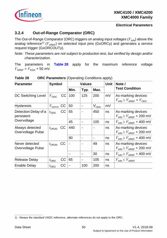
3.2.4 Out-of-Range Comparator (ORC)The Out-of-Range Comparator (ORC) triggers on analog input voltages (VAIN) above theanalog reference1) (VAREF) on selected input pins (GxORCy) and generates a servicerequest trigger (GxORCOUTy).Note: These parameters are not subject to production test, but verified by design and/or
characterization.
The parameters in Table 28 apply for the maximum reference voltageVAREF = VDDA + 50 mV.
1) Always the standard VADC reference, alternate references do not apply to the ORC.
Table 28 ORC Parameters (Operating Conditions apply)
Parameter Symbol Values Unit Note / Test ConditionMin. Typ. Max.
DC Switching Level VODC CC 100 125 200 mV Ax-marking devicesVAIN ≥ VAREF + VODC
Hysteresis VOHYS CC 50 − VODC mVDetection Delay of a persistent Overvoltage
tODD CC 55 − 450 ns Ax-marking devicesVAIN ≥ VAREF + 200 mV
45 − 105 ns VAIN ≥ VAREF + 400 mVAlways detected Overvoltage Pulse
tOPDD CC 440 − − ns Ax-marking devicesVAIN ≥ VAREF + 200 mV
90 − − ns VAIN ≥ VAREF + 400 mVNever detected Overvoltage Pulse
tOPDN CC − − 49 ns Ax-marking devicesVAIN ≥ VAREF + 200 mV
− − 30 ns VAIN ≥ VAREF + 400 mVRelease Delay tORD CC 65 − 105 ns VAIN ≤ VAREF
Enable Delay tOED CC − 100 200 ns
Subject to Agreement on the Use of Product Information

XMC4100 / XMC4200XMC4000 Family
Electrical Parameters
Data Sheet 51 V1.4, 2018-09
Figure 16 GxORCOUTy Trigger Generation
Figure 17 ORC Detection Ranges
VSS
VAREF
tORD
V OD
C
V OH
YS
tODD
GxORCOUTy
GxORCy
VAIN (V)
VAREF + 400 mV
t
VAREF + 200 mV
Overvoltage may be
detected(level uncertain)
Never detected
Overvoltage Pulse
(Too short)
T < tOPDNtOPDN < T < tOPDD
Overvoltage may be
detected
T > tOPDD
Always detected Overvoltage Pulse
T < tOPDN
Never detected
Overvoltage Pulse
(Too short)
tOPDN < T < tOPDD T > tOPDD
Always detected Overvoltage Pulse
VAREF + 100 mV
Overvoltage may be
detected
T > tOPDN
Never detected
Overvoltage Pulse
(Too low)
VAREF
Subject to Agreement on the Use of Product Information

XMC4100 / XMC4200XMC4000 Family
Electrical Parameters
Data Sheet 52 V1.4, 2018-09
3.2.5 High Resolution PWM (HRPWM)The following chapters describe the operating conditions, characteristics and timingrequirements, for all the components inside the HRPWM module. Each description isgiven for just one sub unit, e.g., one CSG or one HRC.All the timing information is related to the module clock, fhrpwm.Note: These parameters are not subject to production test, but verified by design and/or
characterization.
3.2.5.1 HRC characteristicsTable 29 summarizes the characteristics of the HRC units.
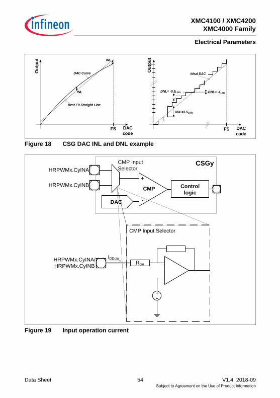
3.2.5.2 CMP and 10-bit DAC characteristicsThe Table 30 summarizes the characteristics of the CSG unit.The specified characteristics require that the setup of the HRPWM follows theinitialization sequence as documented in the Reference Manual.
Table 29 HRC characteristics (Operating Conditions apply)
Parameter Symbol Values Unit Note / Test ConditionMin. Typ. Max.
High resolution step size1)2)
1) The step size for clock frequencies equal to 180, 120 and 80 MHz is 150 ps.2) The step size for clock frequencies different from 180, 120 and 80 MHz but within the range from 180 to 64
MHz can be between 118 to 180 ps (fixed over process and operating conditions)
tHRS CC – 150 – ps
Startup time (after reset release)
tstart CC – – 2 μs
Table 30 CMP and 10-bit DAC characteristics (Operating Conditions apply)
Parameter Symbol Values Unit Note / Test ConditionMin. Typ. Max.
DAC Resolution RESCC
10 bits
DAC differential nonlinearity
DNLCC
-1 – 1.5 LSB Monotonic behavior,See Figure 18
DAC integral nonlinearity INL CC -3 – 3 LSB See Figure 18
Subject to Agreement on the Use of Product Information

XMC4100 / XMC4200XMC4000 Family
Electrical Parameters
Data Sheet 53 V1.4, 2018-09
CSG Output Jitter DCSGCC
– – 1 clk
Bias startup time tstart CC – – 98 usBias supply current IDDbias
CC– – 400 μA
CSGy startup time tCSGSCC
– – 2 μs
Input operation current1) IDDCINCC
-10 – 33 μA See Figure 19
High Speed ModeDAC output voltage range VDOUT
CCVSS – VDDP V
DAC propagation delay - Full scale
tFShsCC
– – 80 ns See Figure 20
Input Selector propagation delay - Full scale
tDhs CC – – 100 ns See Figure 20
Comparator bandwidth tDhs CC 20 – – nsDAC CLK frequency fclk SR – – 30 MHzSupply current IDDhs
CC– – 940 μA
Low Speed ModeDAC output voltage range VDOUT
CC0.1 ×VDDP
2)– VDDP V
DAC propagation delay - Full Scale
tFSls CC – – 160 ns See Figure 20
Input Selector propagation delay - Full Scale
tDls CC – – 200 ns See Figure 20
Comparator bandwidth tDls CC 20 – – nsDAC CLK frequency fclk SR – – 30 MHzSupply current IDDls
CC– – 300 μA
1) Typical input resistance RCIN = 100kOhm.2) The INL error increases for DAC output voltages below this limit.
Table 30 CMP and 10-bit DAC characteristics (Operating Conditions apply)
Parameter Symbol Values Unit Note / Test ConditionMin. Typ. Max.
Subject to Agreement on the Use of Product Information
XMC4100 / XMC4200XMC4000 Family
Electrical Parameters
Data Sheet 54 V1.4, 2018-09
Figure 18 CSG DAC INL and DNL example
Figure 19 Input operation current
Out
put
DAC code
FS
INL
Best Fit Straight Line
Out
put
DAC code
FS
Ideal DAC
DNL=1.5LSBs
DNL= -0.5LSBs
DAC Curve
INL
DNL= -1LSB
CMP Input Selector
CSGy
+
-
CMP
DAC
HRPWMx.CyINA
HRPWMx.CyINB Control logic
HRPWMx.CyINA/HRPWMx.CyINB
IDDcin
CMP Input Selector
Rcin
Subject to Agreement on the Use of Product Information

XMC4100 / XMC4200XMC4000 Family
Electrical Parameters
Data Sheet 55 V1.4, 2018-09
Figure 20 DAC and Input Selector Propagation Delay
3.2.5.3 ClocksHRPWM DAC Conversion ClockThe DAC conversion clock can be generated internally or it can be controlled via aHRPWM module pin.
CSG External ClockIt is possible to select an external source, that can be used as a clock for the slopegeneration, HRPWMx.ECLKy. This clock is synchronized internally with the moduleclock and therefore the external clock needs to meet the criterion described on Table 32.
Table 31 External DAC conversion trigger operating conditionsParameter Symbol Values Unit Note /
Test Condition
Min. Typ. Max.
Frequency fetrg SR – – 302) MHzON time tonetrg SR 2Tccu
1)2)
1) 50% duty cycle is not obligatory2) Only valid if the signal was not previously synchronized/generated with the fccu clock (or a synchronous clock)
– – nsOFF time toffetrg SR 2Tccu
1)2) – – ns
0x000
FS
tfshs/tsishs
t
tfshs/tsishs
CSGyCMP Input Selector
0 V
3.3 V
CSGy
+
-
CMP
DAC0x000
FS
tsishs
tfshs
Out
put
+
-
CMP
DAC
1LSB
1LSB
Subject to Agreement on the Use of Product Information
XMC4100 / XMC4200XMC4000 Family
Electrical Parameters
Data Sheet 56 V1.4, 2018-09
3.2.6 Low Power Analog Comparator (LPAC)
The Low Power Analog Comparator (LPAC) triggers a wake-up event from Hibernatestate or an interrupt trigger during normal operation. It does so by comparing VBAT oranother external sensor voltage VLPS with a pre-programmed threshold voltage.Note: These parameters are not subject to production test, but verified by design and/or
characterization.
Table 32 External clock operating conditionsParameter Symbol Values Unit Note /
Test Condition
Min. Typ. Max.
Frequency feclk SR – – fhrpwm/4 MHzON time toneclk SR 2Tccu
1)2)
1) 50% duty cycle is not obligatory2) Only valid if the signal was not previously synchronized/generated with the fccu clock (or a synchronous clock)
– – nsOFF time toffeclk SR 2Tccu
1)2) – – ns Only the rising edge is used
Table 33 Low Power Analog Comparator ParametersParameter Symbol Values Unit Note /
Test ConditionMin. Typ. Max.VBAT supply voltage range for LPAC operation
VBAT SR 2.1 − 3.6 V
Sensor voltage range VLPCSCC
0 − 1.2 V
Threshold step size Vth CC − 18.75 − mVThreshold trigger accuracy ΔVth CC − − ±10 % for Vth > 0.4 VConversion time tLPCC CC − − 250 μsAverage current consumption over time
ILPCACCC
− − 15 μA conversion interval 10 ms1)
1) Single channel conversion, measuring VBAT = 3.3 V, 8 cycles settling time
Current consumption during conversion
ILPCC CC − 150 − μA 1)
Subject to Agreement on the Use of Product Information
XMC4100 / XMC4200XMC4000 Family
Electrical Parameters
Data Sheet 57 V1.4, 2018-09
3.2.7 Die Temperature Sensor
The Die Temperature Sensor (DTS) measures the junction temperature TJ.Note: These parameters are not subject to production test, but verified by design and/or
characterization.
The following formula calculates the temperature measured by the DTS in [oC] from theRESULT bit field of the DTSSTAT register.
Temperature TDTS = (RESULT - 605) / 2.05 [°C]
This formula and the values defined in Table 34 apply with the following calibrationvalues:• DTSCON.BGTRIM = 8H• DTSCON.REFTRIM = 4H
Table 34 Die Temperature Sensor ParametersParameter Symbol Values Unit Note /
Test ConditionMin. Typ. Max.Temperature sensor range TSR SR -40 − 150 °CLinearity Error(to the below defined formula)
ΔTLE CC − ±1 − °C per ΔTJ ≤ 30 °C
Offset Error ΔTOE CC − ±6 − °C ΔTOE = TJ - TDTSVDDP ≤ 3.3 V1)
1) At VDDP_max = 3.63 V the typical offset error increases by an additional ΔTOE = ±1 °C.
Measurement time tM CC − − 100 μsStart-up time after reset inactive
tTSST SR − − 10 μs
Subject to Agreement on the Use of Product Information

XMC4100 / XMC4200XMC4000 Family
Electrical Parameters
Data Sheet 58 V1.4, 2018-09
3.2.8 USB Device Interface DC CharacteristicsThe Universal Serial Bus (USB) Interface is compliant to the USB Rev. 2.0 Specification.High-Speed Mode is not supported. Note: These parameters are not subject to production test, but verified by design and/or
characterization.
Table 35 USB Device Data Line (USB_DP, USB_DM) Parameters (Operating Conditions apply)
Parameter Symbol Values Unit Note / Test ConditionMin. Typ. Max.
Input low voltage VIL SR − − 0.8 VInput high voltage (driven)
VIH SR 2.0 − − V
Input high voltage (floating) 1)
1) Measured at A-connector with 1.5 kOhm ± 5% to 3.3 V ± 0.3 V connected to USB_DP or USB_DM and at B-connector with 15 kOhm ± 5% to ground connected to USB_DP and USB_DM.
VIHZ SR 2.7 − 3.6 V
Differential input sensitivity
VDIS CC 0.2 − − V
Differential common mode range
VCM CC 0.8 − 2.5 V
Output low voltage VOL CC 0.0 − 0.3 V 1.5 kOhm pull-up to 3.6 V
Output high voltage VOH CC 2.8 − 3.6 V 15 kOhm pull-down to 0 V
DP pull-up resistor (idle bus)
RPUI CC 900 − 1 575 Ohm
DP pull-up resistor (upstream port receiving)
RPUA CC 1 425 − 3 090 Ohm
Input impedance DP, DM
ZINP CC 300 − − kOhm 0 V ≤ VIN ≤ VDDP
Driver output resistance DP, DM
ZDRV CC 28 − 44 Ohm
Subject to Agreement on the Use of Product Information

XMC4100 / XMC4200XMC4000 Family
Electrical Parameters
Data Sheet 59 V1.4, 2018-09
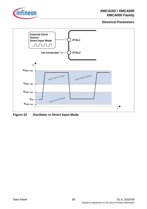
3.2.9 Oscillator Pins
Note: It is strongly recommended to measure the oscillation allowance (negativeresistance) in the final target system (layout) to determine the optimal parametersfor the oscillator operation. Please refer to the limits specified by the crystal orceramic resonator supplier.
Note: These parameters are not subject to production test, but verified by design and/orcharacterization.
The oscillator pins can be operated with an external crystal (see Figure 21) or in directinput mode (see Figure 22).
Figure 21 Oscillator in Crystal Mode
XTAL1
XTAL2
fOSC
Damping resistor may be needed for some crystals
VPPX
VPPX_min ≤ VPPX ≤ VPPX_max
t
V
VPPX_min
tOSCS
GND
Subject to Agreement on the Use of Product Information
XMC4100 / XMC4200XMC4000 Family
Electrical Parameters
Data Sheet 60 V1.4, 2018-09
Figure 22 Oscillator in Direct Input Mode
V
VIHBX_max
VSS
t
Input High Voltage
Input Low Voltage
Input High Voltage
XTAL1
XTAL2not connected
External Clock SourceDirect Input Mode
VIHBX_min
VILBX_max
VILBX_min
Subject to Agreement on the Use of Product Information

XMC4100 / XMC4200XMC4000 Family
Electrical Parameters
Data Sheet 61 V1.4, 2018-09
Table 36 OSC_XTAL ParametersParameter Symbol Values Unit Note /
Test ConditionMin. Typ. Max.Input frequency fOSC SR 4 − 40 MHz Direct Input Mode
selected4 − 25 MHz External Crystal
Mode selectedOscillator start-up time1)2)
1) tOSCS is defined from the moment the oscillator is enabled wih SCU_OSCHPCTRL.MODE until the oscillationsreach an amplitude at XTAL1 of 0.4 * VDDP.
2) The external oscillator circuitry must be optimized by the customer and checked for negative resistance andamplitude as recommended and specified by crystal suppliers.
tOSCSCC
− − 10 ms
Input voltage at XTAL1 VIX SR -0.5 − VDDP + 0.5
V
Input amplitude (peak-to-peak) at XTAL12)3)
3) If the shaper unit is enabled and not bypassed.
VPPX SR 0.4 ×VDDP
− VDDP + 1.0
V
Input high voltage at XTAL14)
4) If the shaper unit is bypassed, dedicated DC-thresholds have to be met.
VIHBXSR 1.0 − VDDP + 0.5
V
Input low voltage at XTAL14)
VILBX SR -0.5 − 0.4 V
Input leakage current at XTAL1
IILX1 CC -100 − 100 nA Oscillator power down0 V ≤ VIX ≤ VDDP
Subject to Agreement on the Use of Product Information
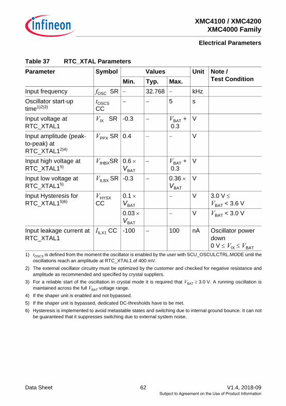
XMC4100 / XMC4200XMC4000 Family
Electrical Parameters
Data Sheet 62 V1.4, 2018-09
Table 37 RTC_XTAL ParametersParameter Symbol Values Unit Note /
Test ConditionMin. Typ. Max.Input frequency fOSC SR − 32.768 − kHzOscillator start-up time1)2)3)
1) tOSCS is defined from the moment the oscillator is enabled by the user with SCU_OSCULCTRL.MODE until theoscillations reach an amplitude at RTC_XTAL1 of 400 mV.
2) The external oscillator circuitry must be optimized by the customer and checked for negative resistance andamplitude as recommended and specified by crystal suppliers.
3) For a reliable start of the oscillation in crystal mode it is required that VBAT ≥ 3.0 V. A running oscillation ismaintained across the full VBAT voltage range.
tOSCS CC
− − 5 s
Input voltage at RTC_XTAL1
VIX SR -0.3 − VBAT +0.3
V
Input amplitude (peak-to-peak) at RTC_XTAL12)4)
4) If the shaper unit is enabled and not bypassed.
VPPX SR 0.4 − − V
Input high voltage at RTC_XTAL15)
5) If the shaper unit is bypassed, dedicated DC-thresholds have to be met.
VIHBXSR 0.6 ×VBAT
− VBAT +0.3
V
Input low voltage at RTC_XTAL15)
VILBX SR -0.3 − 0.36 ×VBAT
V
Input Hysteresis for RTC_XTAL15)6)
6) Hysteresis is implemented to avoid metastable states and switching due to internal ground bounce. It can notbe guaranteed that it suppresses switching due to external system noise.
VHYSX CC
0.1 × VBAT
− V 3.0 V ≤ VBAT < 3.6 V
0.03 × VBAT
− V VBAT < 3.0 V
Input leakage current at RTC_XTAL1
IILX1 CC -100 − 100 nA Oscillator power down0 V ≤ VIX ≤ VBAT
Subject to Agreement on the Use of Product Information
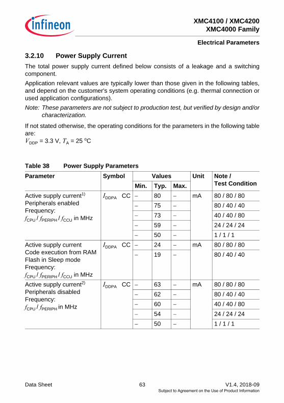
XMC4100 / XMC4200XMC4000 Family
Electrical Parameters
Data Sheet 63 V1.4, 2018-09
3.2.10 Power Supply CurrentThe total power supply current defined below consists of a leakage and a switchingcomponent.Application relevant values are typically lower than those given in the following tables,and depend on the customer's system operating conditions (e.g. thermal connection orused application configurations).Note: These parameters are not subject to production test, but verified by design and/or
characterization.
If not stated otherwise, the operating conditions for the parameters in the following tableare:VDDP = 3.3 V, TA = 25 oC
Table 38 Power Supply ParametersParameter Symbol Values Unit Note /
Test ConditionMin. Typ. Max.Active supply current1)
Peripherals enabledFrequency: fCPU / fPERIPH / fCCU in MHz
IDDPA CC − 80 − mA 80 / 80 / 80− 75 − 80 / 40 / 40− 73 − 40 / 40 / 80− 59 − 24 / 24 / 24− 50 − 1 / 1 / 1
Active supply currentCode execution from RAMFlash in Sleep modeFrequency: fCPU / fPERIPH / fCCU in MHz
IDDPA CC − 24 − mA 80 / 80 / 80− 19 − 80 / 40 / 40
Active supply current2)
Peripherals disabledFrequency: fCPU / fPERIPH in MHz
IDDPA CC − 63 − mA 80 / 80 / 80− 62 − 80 / 40 / 40− 60 − 40 / 40 / 80− 54 − 24 / 24 / 24− 50 − 1 / 1 / 1
Subject to Agreement on the Use of Product Information
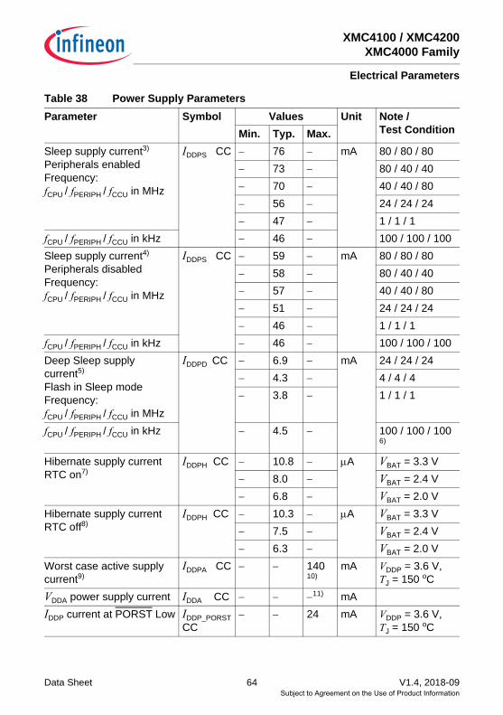
XMC4100 / XMC4200XMC4000 Family
Electrical Parameters
Data Sheet 64 V1.4, 2018-09
Sleep supply current3)
Peripherals enabledFrequency: fCPU / fPERIPH / fCCU in MHz
IDDPS CC − 76 − mA 80 / 80 / 80− 73 − 80 / 40 / 40− 70 − 40 / 40 / 80− 56 − 24 / 24 / 24− 47 − 1 / 1 / 1
fCPU / fPERIPH / fCCU in kHz − 46 − 100 / 100 / 100Sleep supply current4)
Peripherals disabledFrequency: fCPU / fPERIPH / fCCU in MHz
IDDPS CC − 59 − mA 80 / 80 / 80− 58 − 80 / 40 / 40− 57 − 40 / 40 / 80− 51 − 24 / 24 / 24− 46 − 1 / 1 / 1
fCPU / fPERIPH / fCCU in kHz − 46 − 100 / 100 / 100Deep Sleep supply current5)
Flash in Sleep modeFrequency: fCPU / fPERIPH / fCCU in MHz
IDDPD CC − 6.9 − mA 24 / 24 / 24− 4.3 − 4 / 4 / 4− 3.8 − 1 / 1 / 1
fCPU / fPERIPH / fCCU in kHz − 4.5 − 100 / 100 / 1006)
Hibernate supply currentRTC on7)
IDDPH CC − 10.8 − μA VBAT = 3.3 V− 8.0 − VBAT = 2.4 V− 6.8 − VBAT = 2.0 V
Hibernate supply currentRTC off8)
IDDPH CC − 10.3 − μA VBAT = 3.3 V− 7.5 − VBAT = 2.4 V− 6.3 − VBAT = 2.0 V
Worst case active supply current9)
IDDPA CC − − 14010)
mA VDDP = 3.6 V,TJ = 150 oC
VDDA power supply current IDDA CC − − −11) mAIDDP current at PORST Low IDDP_PORST
CC− − 24 mA VDDP = 3.6 V,
TJ = 150 oC
Table 38 Power Supply ParametersParameter Symbol Values Unit Note /
Test ConditionMin. Typ. Max.
Subject to Agreement on the Use of Product Information
XMC4100 / XMC4200XMC4000 Family
Electrical Parameters
Data Sheet 65 V1.4, 2018-09
Power Dissipation PDISS CC − − 1 W VDDP = 3.6 V,TJ = 150 oC
Wake-up time from Sleep to Active mode
tSSA CC − 6 − cycles
Wake-up time from Deep Sleep to Active mode
− − − ms Defined by the wake-up of the Flash module, see Section 3.2.11
Wake-up time from Hibernate mode
− − − ms Wake-up via power-on reset event, see Section 3.3.2
1) CPU executing code from Flash, all peripherals idle.2) CPU executing code from Flash. USB and CCU clock off.3) CPU in sleep, all peripherals idle, Flash in Active mode.4) CPU in sleep, Flash in Active mode.5) CPU in sleep, peripherals disabled, after wake-up code execution from RAM.6) To wake-up the Flash from its Sleep mode, fCPU ≥ 1 MHz is required.7) OSC_ULP operating with external crystal on RTC_XTAL8) OSC_ULP off, Hibernate domain operating with OSC_SI clock9) Test Power Loop: fSYS = 80 MHz, CPU executing benchmark code from Flash, all CCUs in 100kHz timer mode,
all ADC groups in continuous conversion mode, USICs as SPI in internal loop-back mode, CAN in 500kHzinternal loop-back mode, interrupt triggered DMA block transfers to parity protected RAMs and FCE, DTSmeasurements and FPU calculations.The power consumption of each customer application will most probably be lower than this value, but must beevaluated separately.
10) IDDP decreases typically by 3.5 mA when fSYS decreases by 10 MHz, at constant TJ
11) Sum of currents of all active converters (ADC and DAC)
Table 38 Power Supply ParametersParameter Symbol Values Unit Note /
Test ConditionMin. Typ. Max.
Subject to Agreement on the Use of Product Information
XMC4100 / XMC4200XMC4000 Family
Electrical Parameters
Data Sheet 66 V1.4, 2018-09
Peripheral Idle CurrentsTest conditions:• fsys and derived clocks at 80 MHz• VDDP = 3.3 V, Ta =25 °C• all peripherals are held in reset (see the PRSTAT registers in the Reset Control Unit
of the SCU)• the peripheral clocks are disabled (see CGATSTAT registers in the Clock Control
Unit of the SCU• no I/O activity• the given values are a result of differential measurements with asserted and
deasserted peripheral reset and enabled clock of the peripheral under testThe tested peripheral is left in the state after the peripheral reset is deasserted, no furtherinitialisation or configuration is done. E.g. no timer is running in the CCUs, nocommunication active in the USICs, etc.
Table 39 Peripheral Idle CurrentsParameter Symbol Values Unit Note /
Test ConditionMin. Typ. Max.PORTSUSBFCEWDTPOSIFx1)
1) Enabling the fCCU clock for the POSIFx/CCU4x/CCU8x modules adds approximately IPER = 1.8 mA,disregarding which and how many of those peripherals are enabled.
IPER CC − ≤ 0.3 − mA
MultiCANERULEDTSCU0CCU4x1)
CCU8x1)
− ≤ 1.0 −
DAC (digital)2)
2) The current consumption of the analog components are given in the dedicated Data Sheet sections of therespective peripheral.
− 1.3 −
USICx − 3.0 −
VADC (digital)2) − 4.5 −
DMAx − 6.0 −
Subject to Agreement on the Use of Product Information

XMC4100 / XMC4200XMC4000 Family
Electrical Parameters
Data Sheet 67 V1.4, 2018-09
3.2.11 Flash Memory Parameters
Note: These parameters are not subject to production test, but verified by design and/orcharacterization.
Table 40 Flash Memory ParametersParameter Symbol Values Unit Note /
Test ConditionMin. Typ. Max.Erase Time per 256 Kbyte Sector
tERP CC − 5 5.5 s
Erase Time per 64 Kbyte Sector
tERP CC − 1.2 1.4 s
Erase Time per 16 Kbyte Logical Sector
tERP CC − 0.3 0.4 s
Program time per page1) tPRP CC − 5.5 11 msErase suspend delay tFL_ErSusp
CC− − 15 ms
Wait time after margin change
tFL_Margin
Del CC10 − − μs
Wake-up time tWU CC − − 270 μsRead access time ta CC 20 − − ns For operation
with 1 / fCPU < ta wait states must be configured2)
Data Retention Time, Physical Sector3)4)
tRET CC 20 − − years Max. 1000 erase/program cycles
Data Retention Time, Logical Sector3)4)
tRETL CC 20 − − years Max. 100 erase/program cycles
Subject to Agreement on the Use of Product Information
XMC4100 / XMC4200XMC4000 Family
Electrical Parameters
Data Sheet 68 V1.4, 2018-09
Data Retention Time, User Configuration Block (UCB)3)4)
tRTU CC 20 − − years Max. 4 erase/program cycles per UCB
Endurance on 64 Kbyte Physical Sector PS4
NEPS4 CC
10000 − − cycles BA-marking devices only!Cycling distributed over life time5)
1) In case the Program Verify feature detects weak bits, these bits will be programmed once more. Thereprogramming takes an additional time of 5.5 ms.
2) The following formula applies to the wait state configuration: FCON.WSPFLASH × (1 / fCPU) ≥ ta.3) Storage and inactive time included.4) Values given are valid for an average weighted junction temperature of TJ = 110°C.5) Only valid with robust EEPROM emulation algorithm, equally cycling the logical sectors. For more details see
the Reference Manual.
Table 40 Flash Memory ParametersParameter Symbol Values Unit Note /
Test ConditionMin. Typ. Max.
Subject to Agreement on the Use of Product Information
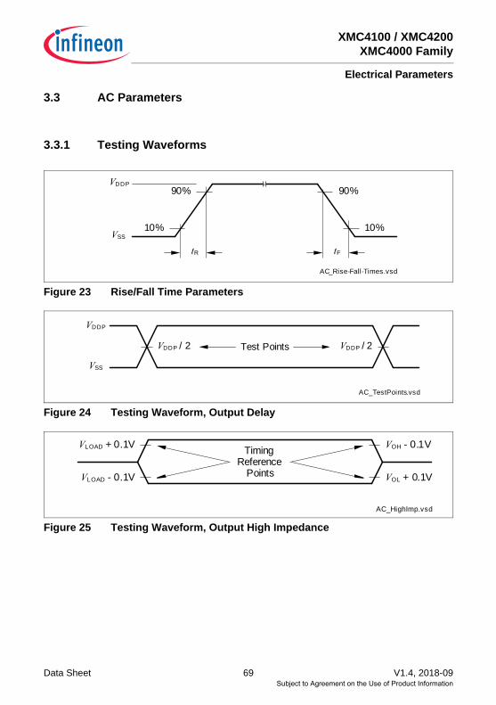
XMC4100 / XMC4200XMC4000 Family
Electrical Parameters
Data Sheet 69 V1.4, 2018-09
3.3 AC Parameters
3.3.1 Testing Waveforms
Figure 23 Rise/Fall Time Parameters
Figure 24 Testing Waveform, Output Delay
Figure 25 Testing Waveform, Output High Impedance
AC_Rise-Fall-Times.vsd
10%
90%
VSS
VDDP
tR tF
10%
90%
AC_TestPoints.vsd
VDDP / 2 VDDP / 2
VDDP
VSS
Test Points
AC_HighImp.vsd
VLOAD + 0.1V Timing Reference
PointsVLOAD - 0.1V
VOH - 0.1V
VOL + 0.1V
Subject to Agreement on the Use of Product Information
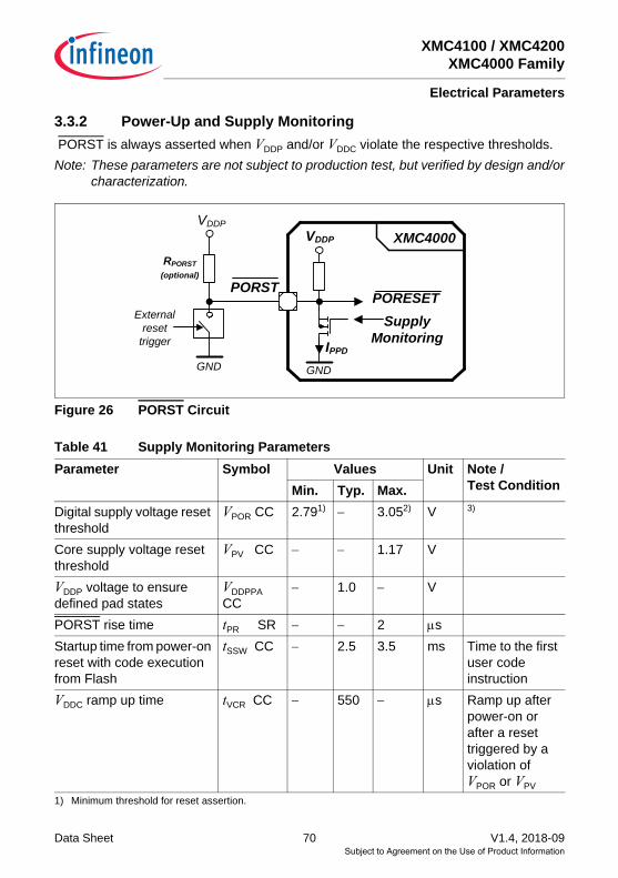
XMC4100 / XMC4200XMC4000 Family
Electrical Parameters
Data Sheet 70 V1.4, 2018-09
3.3.2 Power-Up and Supply Monitoring PORST is always asserted when VDDP and/or VDDC violate the respective thresholds.Note: These parameters are not subject to production test, but verified by design and/or
characterization.
Figure 26 PORST Circuit
Table 41 Supply Monitoring ParametersParameter Symbol Values Unit Note /
Test ConditionMin. Typ. Max.Digital supply voltage reset threshold
VPOR CC 2.791)
1) Minimum threshold for reset assertion.
− 3.052) V 3)
Core supply voltage reset threshold
VPV CC − − 1.17 V
VDDP voltage to ensure defined pad states
VDDPPA CC
− 1.0 − V
PORST rise time tPR SR − − 2 μsStartup time from power-on reset with code execution from Flash
tSSW CC − 2.5 3.5 ms Time to the first user code instruction
VDDC ramp up time tVCR CC − 550 − μs Ramp up after power-on or after a reset triggered by a violation of VPOR or VPV
VDDP
PORST
GND
PORESET
VDDP
GND
XMC4000RPORST
(optional)
External reset
trigger
Supply MonitoringIPPD
Subject to Agreement on the Use of Product Information

XMC4100 / XMC4200XMC4000 Family
Electrical Parameters
Data Sheet 71 V1.4, 2018-09
Figure 27 Power-Up Behavior
3.3.3 Power SequencingWhile starting up and shutting down as well as when switching power modes of thesystem it is important to limit the current load steps. A typical cause for such load stepsis changing the CPU frequency fCPU. Load steps exceeding the below defined valuesmay cause a power on reset triggered by the supply monitor.Note: These parameters are not subject to production test, but verified by design and/or
characterization.
2) Maximum threshold for reset deassertion.3) The VDDP monitoring has a typical hysteresis of VPORHYS = 180 mV.
as programmed
VPOR
VPV
VDDP
VDDC
Pads
PORST
VDDPPA
UndefinedHigh-impedance or pull -device active
3.3 V
1.3 V
tSSW
tVCR
tPR
Subject to Agreement on the Use of Product Information

XMC4100 / XMC4200XMC4000 Family
Electrical Parameters
Data Sheet 72 V1.4, 2018-09
Positive Load Step ExamplesSystem assumptions:fCPU = fSYS, target frequency fCPU = 80 MHz, main PLL fVCO = 480 MHz, stepping done byK2 divider, tPLSS between individual steps:24 MHz - 48 MHz - 80 MHz (K2 steps 20 - 10 - 6)24 MHz - 60 MHz - 80 MHz (K2 steps 20 - 8 - 6)
Table 42 Power Sequencing ParametersParameter Symbol Values Unit Note /
Test ConditionMin. Typ. Max.Positive Load Step Current ΔIPLS SR - − 50 mA Load increase
on VDDPΔt ≤ 10 ns
Negative Load Step Current
ΔINLS SR - − 150 mA Load decrease on VDDPΔt ≤ 10 ns
VDDC Voltage Over-/ Undershoot from Load
Step
ΔVLS CC - − ±100 mV For maximum positive or negative load step
Positive Load Step Settling Time
tPLSS SR 50 − - μs
Negative Load Step Settling Time
tNLSS SR 100 − - μs
External Buffer Capacitor on VDDC
CEXT SR 3 4.7 6 μF In addition C = 100 nF capacitor on each VDDC pin
Subject to Agreement on the Use of Product Information
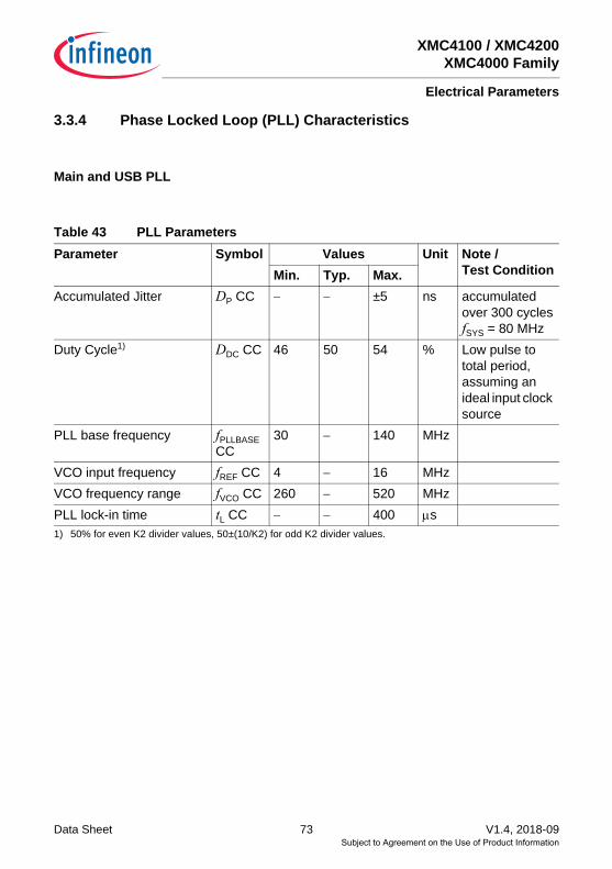
XMC4100 / XMC4200XMC4000 Family
Electrical Parameters
Data Sheet 73 V1.4, 2018-09
3.3.4 Phase Locked Loop (PLL) Characteristics
Main and USB PLL
Table 43 PLL ParametersParameter Symbol Values Unit Note /
Test ConditionMin. Typ. Max.Accumulated Jitter DP CC − − ±5 ns accumulated
over 300 cyclesfSYS = 80 MHz
Duty Cycle1)
1) 50% for even K2 divider values, 50±(10/K2) for odd K2 divider values.
DDC CC 46 50 54 % Low pulse to total period,assuming an ideal input clock source
PLL base frequency fPLLBASE CC
30 − 140 MHz
VCO input frequency fREF CC 4 − 16 MHzVCO frequency range fVCO CC 260 − 520 MHzPLL lock-in time tL CC − − 400 μs
Subject to Agreement on the Use of Product Information
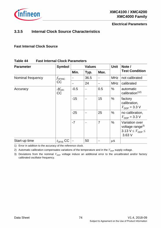
XMC4100 / XMC4200XMC4000 Family
Electrical Parameters
Data Sheet 74 V1.4, 2018-09
3.3.5 Internal Clock Source Characteristics
Fast Internal Clock Source
Table 44 Fast Internal Clock ParametersParameter Symbol Values Unit Note /
Test ConditionMin. Typ. Max.Nominal frequency fOFINC
CC− 36.5 − MHz not calibrated− 24 − MHz calibrated
Accuracy ΔfOFI CC
-0.5 − 0.5 % automatic calibration1)2)
1) Error in addition to the accuracy of the reference clock.2) Automatic calibration compensates variations of the temperature and in the VDDP supply voltage.
-15 − 15 % factory calibration,VDDP = 3.3 V
-25 − 25 % no calibration,VDDP = 3.3 V
-7 − 7 % Variation over voltage range3)
3.13 V ≤ VDDP ≤3.63 V
3) Deviations from the nominal VDDP voltage induce an additional error to the uncalibrated and/or factorycalibrated oscillator frequency.
Start-up time tOFIS CC − 50 − μs
Subject to Agreement on the Use of Product Information
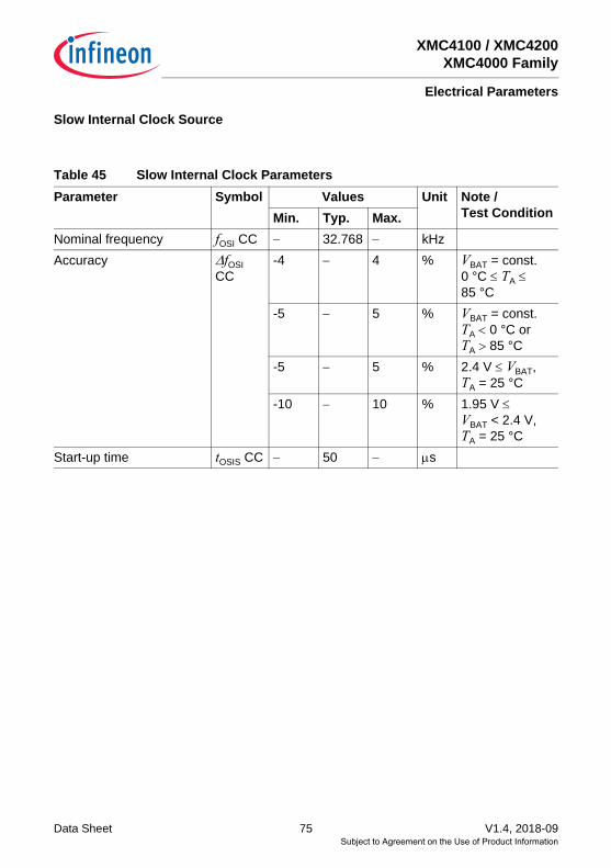
XMC4100 / XMC4200XMC4000 Family
Electrical Parameters
Data Sheet 75 V1.4, 2018-09
Slow Internal Clock Source
Table 45 Slow Internal Clock ParametersParameter Symbol Values Unit Note /
Test ConditionMin. Typ. Max.Nominal frequency fOSI CC − 32.768 − kHzAccuracy ΔfOSI
CC-4 − 4 % VBAT = const.
0 °C ≤ TA ≤ 85 °C
-5 − 5 % VBAT = const.TA < 0 °C orTA > 85 °C
-5 − 5 % 2.4 V ≤ VBAT,TA = 25 °C
-10 − 10 % 1.95 V ≤ VBAT < 2.4 V,TA = 25 °C
Start-up time tOSIS CC − 50 − μs
Subject to Agreement on the Use of Product Information
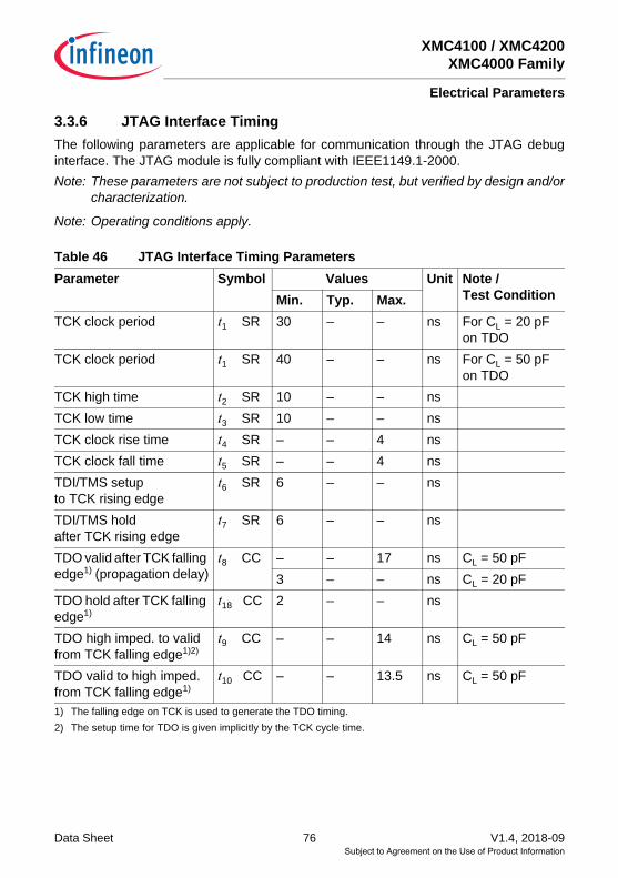
XMC4100 / XMC4200XMC4000 Family
Electrical Parameters
Data Sheet 76 V1.4, 2018-09
3.3.6 JTAG Interface TimingThe following parameters are applicable for communication through the JTAG debuginterface. The JTAG module is fully compliant with IEEE1149.1-2000.Note: These parameters are not subject to production test, but verified by design and/or
characterization.
Note: Operating conditions apply.
Table 46 JTAG Interface Timing ParametersParameter Symbol Values Unit Note /
Test ConditionMin. Typ. Max.TCK clock period t1 SR 30 – – ns For CL = 20 pF
on TDOTCK clock period t1 SR 40 – – ns For CL = 50 pF
on TDOTCK high time t2 SR 10 – – nsTCK low time t3 SR 10 – – nsTCK clock rise time t4 SR – – 4 nsTCK clock fall time t5 SR – – 4 nsTDI/TMS setupto TCK rising edge
t6 SR 6 – – ns
TDI/TMS holdafter TCK rising edge
t7 SR 6 – – ns
TDO valid after TCK falling edge1) (propagation delay)
1) The falling edge on TCK is used to generate the TDO timing.
t8 CC – – 17 ns CL = 50 pF3 – – ns CL = 20 pF
TDO hold after TCK falling edge1)
t18 CC 2 – – ns
TDO high imped. to validfrom TCK falling edge1)2)
2) The setup time for TDO is given implicitly by the TCK cycle time.
t9 CC – – 14 ns CL = 50 pF
TDO valid to high imped.from TCK falling edge1)
t10 CC – – 13.5 ns CL = 50 pF
Subject to Agreement on the Use of Product Information
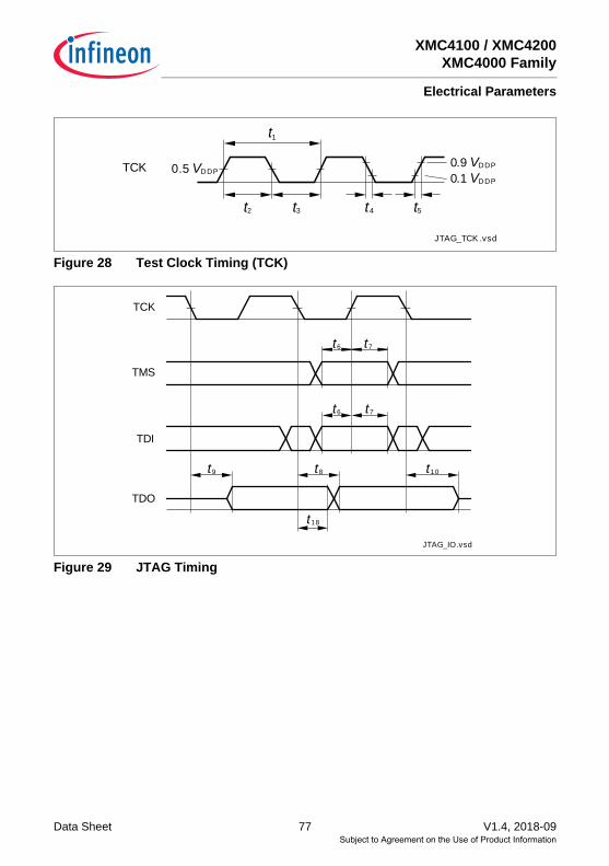
XMC4100 / XMC4200XMC4000 Family
Electrical Parameters
Data Sheet 77 V1.4, 2018-09
Figure 28 Test Clock Timing (TCK)
Figure 29 JTAG Timing
JTAG_TCK .vsd
0.9 VDDP0.5 VDDPTCK
t1
t2
0.1 VDDP
t3 t5t4
JTAG_IO.vsd
t6 t7
t6 t7
t9 t8 t10
TCK
TMS
TDI
TDO
t18
Subject to Agreement on the Use of Product Information
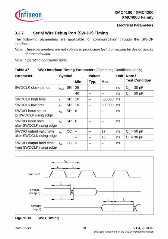
XMC4100 / XMC4200XMC4000 Family
Electrical Parameters
Data Sheet 78 V1.4, 2018-09
3.3.7 Serial Wire Debug Port (SW-DP) TimingThe following parameters are applicable for communication through the SW-DPinterface.Note: These parameters are not subject to production test, but verified by design and/or
characterization.
Note: Operating conditions apply.
Figure 30 SWD Timing
Table 47 SWD Interface Timing Parameters (Operating Conditions apply)
Parameter Symbol Values Unit Note / Test ConditionMin. Typ. Max.
SWDCLK clock period tSC SR 25 – – ns CL = 30 pF40 – – ns CL = 50 pF
SWDCLK high time t1 SR 10 – 500000 nsSWDCLK low time t2 SR 10 – 500000 nsSWDIO input setupto SWDCLK rising edge
t3 SR 6 – – ns
SWDIO input holdafter SWDCLK rising edge
t4 SR 6 – – ns
SWDIO output valid time after SWDCLK rising edge
t5 CC – – 17 ns CL = 50 pF– – 13 ns CL = 30 pF
SWDIO output hold time from SWDCLK rising edge
t6 CC 3 – – ns
SWDCLK
SWDIO(Output)
t1 t2
t6
t5
tSC
SWDIO(Input)
t3 t4
Subject to Agreement on the Use of Product Information

XMC4100 / XMC4200XMC4000 Family
Electrical Parameters
Data Sheet 79 V1.4, 2018-09
3.3.8 Peripheral Timing
Note: These parameters are not subject to production test, but verified by design and/orcharacterization.
Note: Operating conditions apply.
3.3.8.1 Synchronous Serial Interface (USIC SSC) TimingThe following parameters are applicable for a USIC channel operated in SSC mode.Note: Operating Conditions apply.
Table 48 USIC SSC Master Mode TimingParameter Symbol Values Unit Note /
Test ConditionMin. Typ. Max.SCLKOUT master clock period
tCLK CC 40 − − ns
Slave select output SELO active to first SCLKOUT transmit edge
t1 CC tSYS - 6.51)
1) tSYS = 1 / fPB
− − ns
Slave select output SELO inactive after last SCLKOUT receive edge
t2 CC tSYS - 8.51)
− − ns
Data output DOUT[3:0] valid time
t3 CC -6 − 8 ns
Receive data input DX0/DX[5:3] setup time to SCLKOUT receive edge
t4 SR 23 − − ns
Data input DX0/DX[5:3] hold time from SCLKOUT receive edge
t5 SR 1 − − ns
Subject to Agreement on the Use of Product Information
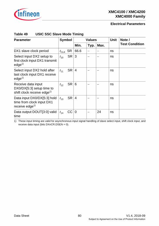
XMC4100 / XMC4200XMC4000 Family
Electrical Parameters
Data Sheet 80 V1.4, 2018-09
Table 49 USIC SSC Slave Mode TimingParameter Symbol Values Unit Note /
Test ConditionMin. Typ. Max.DX1 slave clock period tCLK SR 66.6 − − nsSelect input DX2 setup to first clock input DX1 transmit edge1)
1) These input timing are valid for asynchronous input signal handling of slave select input, shift clock input, andreceive data input (bits DXnCR.DSEN = 0).
t10 SR 3 − − ns
Select input DX2 hold after last clock input DX1 receive edge1)
t11 SR 4 − − ns
Receive data input DX0/DX[5:3] setup time to shift clock receive edge1)
t12 SR 6 − − ns
Data input DX0/DX[5:3] hold time from clock input DX1 receive edge1)
t13 SR 4 − − ns
Data output DOUT[3:0] valid time
t14 CC 0 − 24 ns
Subject to Agreement on the Use of Product Information
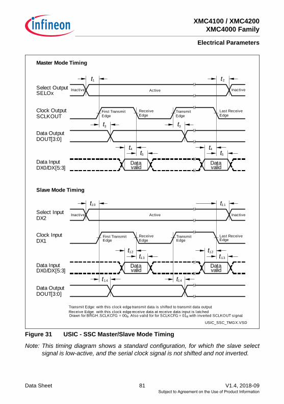
XMC4100 / XMC4200XMC4000 Family
Electrical Parameters
Data Sheet 81 V1.4, 2018-09
Figure 31 USIC - SSC Master/Slave Mode Timing
Note: This timing diagram shows a standard configuration, for which the slave selectsignal is low-active, and the serial clock signal is not shifted and not inverted.
t2t1
USIC_SSC_TMGX.VSD
Clock OutputSCLKOUT
Data OutputDOUT[3:0]
t3 t3
t5
Datavalid
t4
First Transmit Edge
Data InputDX0/DX[5:3]
Select OutputSELOx Active
Master Mode Timing
Slave Mode Timing
t11t10
Clock InputDX1
Data OutputDOUT[3:0]
t14 t14
Datavalid
Data InputDX0/DX[5:3]
Select InputDX2
Active
t13
t12
Transmit Edge: with this clock edge, transmit data is shifted to transmit data output.Receive Edge: with this clock edge, receive data at receive data input is latched.
Receive Edge
Last Receive Edge
InactiveInactive
Transmit Edge
InactiveInactive
First Transmit Edge
Receive Edge
Transmit Edge
Last Receive Edge
t5
Datavalid
t4
Datavalid
t12
t13
Drawn for BRGH.SCLKCFG = 00B. Also valid for for SCLKCFG = 01B with inverted SCLKOUT signal.
Subject to Agreement on the Use of Product Information

XMC4100 / XMC4200XMC4000 Family
Electrical Parameters
Data Sheet 82 V1.4, 2018-09
3.3.8.2 Inter-IC (IIC) Interface TimingThe following parameters are applicable for a USIC channel operated in IIC mode.Note: Operating Conditions apply.
Table 50 USIC IIC Standard Mode Timing1)
1) Due to the wired-AND configuration of an IIC bus system, the port drivers of the SCL and SDA signal linesneed to operate in open-drain mode. The high level on these lines must be held by an external pull-up device,approximalely 10 kOhm for operation at 100 kbit/s, approximately 2 kOhm for operation at 400 kbit/s.
Parameter Symbol Values Unit Note / Test ConditionMin. Typ. Max.
Fall time of both SDA and SCL
t1 CC/SR
- - 300 ns
Rise time of both SDA and SCL
t2 CC/SR
- - 1000 ns
Data hold time t3 CC/SR
0 - - µs
Data set-up time t4 CC/SR
250 - - ns
LOW period of SCL clock t5 CC/SR
4.7 - - µs
HIGH period of SCL clock t6 CC/SR
4.0 - - µs
Hold time for (repeated) START condition
t7 CC/SR
4.0 - - µs
Set-up time for repeated START condition
t8 CC/SR
4.7 - - µs
Set-up time for STOP condition
t9 CC/SR
4.0 - - µs
Bus free time between a STOP and START condition
t10 CC/SR
4.7 - - µs
Capacitive load for each bus line
Cb SR - - 400 pF
Subject to Agreement on the Use of Product Information

XMC4100 / XMC4200XMC4000 Family
Electrical Parameters
Data Sheet 83 V1.4, 2018-09
Table 51 USIC IIC Fast Mode Timing1)
1) Due to the wired-AND configuration of an IIC bus system, the port drivers of the SCL and SDA signal linesneed to operate in open-drain mode. The high level on these lines must be held by an external pull-up device,approximalely 10 kOhm for operation at 100 kbit/s, approximately 2 kOhm for operation at 400 kbit/s.
Parameter Symbol Values Unit Note / Test ConditionMin. Typ. Max.
Fall time of both SDA and SCL
t1 CC/SR
20 + 0.1*Cb2)
2) Cb refers to the total capacitance of one bus line in pF.
- 300 ns
Rise time of both SDA and SCL
t2 CC/SR
20 + 0.1*Cb2)
- 300 ns
Data hold time t3 CC/SR
0 - - µs
Data set-up time t4 CC/SR
100 - - ns
LOW period of SCL clock t5 CC/SR
1.3 - - µs
HIGH period of SCL clock t6 CC/SR
0.6 - - µs
Hold time for (repeated) START condition
t7 CC/SR
0.6 - - µs
Set-up time for repeated START condition
t8 CC/SR
0.6 - - µs
Set-up time for STOP condition
t9 CC/SR
0.6 - - µs
Bus free time between a STOP and START condition
t10 CC/SR
1.3 - - µs
Capacitive load for each bus line
Cb SR - - 400 pF
Subject to Agreement on the Use of Product Information

XMC4100 / XMC4200XMC4000 Family
Electrical Parameters
Data Sheet 84 V1.4, 2018-09
Figure 32 USIC IIC Stand and Fast Mode Timing
3.3.8.3 Inter-IC Sound (IIS) Interface TimingThe following parameters are applicable for a USIC channel operated in IIS mode.Note: Operating Conditions apply.
Table 52 USIC IIS Master Transmitter TimingParameter Symbol Values Unit Note /
Test ConditionMin. Typ. Max.Clock period t1 CC 33.3 − − nsClock high time t2 CC 0.35 x
t1min
− − ns
Clock low time t3 CC 0.35 x t1min
− − ns
Hold time t4 CC 0 − − nsClock rise time t5 CC − − 0.15 x
t1min
ns
SCL
SDA
SCL
SDA
t1 t2
t1 t2
t10
t9t7t8
t7
t3
t4
t5
t6
P SSr
S
70%
30%
9th
clock
9th
clock
Subject to Agreement on the Use of Product Information
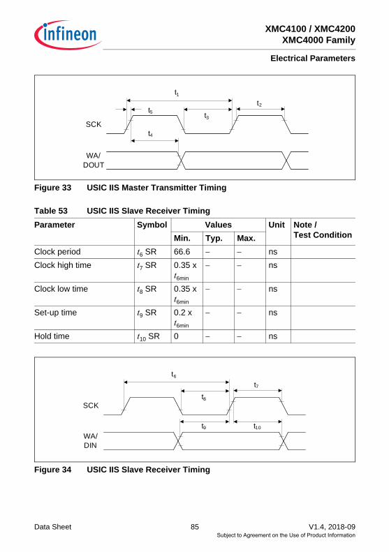
XMC4100 / XMC4200XMC4000 Family
Electrical Parameters
Data Sheet 85 V1.4, 2018-09
Figure 33 USIC IIS Master Transmitter Timing
Figure 34 USIC IIS Slave Receiver Timing
Table 53 USIC IIS Slave Receiver TimingParameter Symbol Values Unit Note /
Test ConditionMin. Typ. Max.Clock period t6 SR 66.6 − − nsClock high time t7 SR 0.35 x
t6min
− − ns
Clock low time t8 SR 0.35 x t6min
− − ns
Set-up time t9 SR 0.2 x t6min
− − ns
Hold time t10 SR 0 − − ns
SCK
WA/DOUT
t1
t5 t3
t2
t4
SCK
WA/DIN
t6
t10
t8
t7
t9
Subject to Agreement on the Use of Product Information

XMC4100 / XMC4200XMC4000 Family
Electrical Parameters
Data Sheet 86 V1.4, 2018-09
3.3.9 USB Interface CharacteristicsThe Universal Serial Bus (USB) Interface is compliant to the USB Rev. 2.0 Specification.High-Speed Mode is not supported. Note: These parameters are not subject to production test, but verified by design and/or
characterization.
Figure 35 USB Signal Timing
Table 54 USB Timing Parameters (operating conditions apply)
Parameter Symbol Values Unit Note / Test ConditionMin. Typ. Max.
Rise time tR CC 4 – 20 ns CL = 50 pFFall time tF CC 4 – 20 ns CL = 50 pFRise/Fall time matching tR/tF CC 90 – 111.11 % CL = 50 pFCrossover voltage VCRS CC 1.3 – 2.0 V CL = 50 pF
USB_Rise-Fall-Times.vsd
10%
90%
D-
D+
tR tF
10%
90%
VCRS
VSS
Subject to Agreement on the Use of Product Information

XMC4100 / XMC4200XMC4000 Family
Package and Reliability
Data Sheet 87 V1.4, 2018-09
4 Package and ReliabilityThe XMC4[12]00 is a member of the XMC4000 Family of microcontrollers. It is alsocompatible to a certain extent with members of similar families or subfamilies.Each package is optimized for the device it houses. Therefore, there may be slightdifferences between packages of the same pin-count but for different device types. Inparticular, the size of the Exposed Die Pad may vary.If different device types are considered or planned for an application, it must be ensuredthat the board layout fits all packages under consideration.
4.1 Package ParametersTable 55 provides the thermal characteristics of the packages used in XMC4[12]00. Theavailability of different packages for different markings is listed in Table 2.
Note: For electrical reasons, it is required to connect the exposed pad to the boardground VSS, independent of EMC and thermal requirements.
4.1.1 Thermal ConsiderationsWhen operating the XMC4[12]00 in a system, the total heat generated in the chip mustbe dissipated to the ambient environment to prevent overheating and the resultingthermal damage.The maximum heat that can be dissipated depends on the package and its integrationinto the target board. The “Thermal resistance RΘJA” quantifies these parameters. The
Table 55 Thermal Characteristics of the PackagesParameter Symbol Limit Values Unit Package Types
Min. Max.Exposed Die Pad Dimensions
Ex × EyCC
- 5.8 × 5.8 mm PG-LQFP-64-19- 5.7 × 5.7 mm PG-TQFP-64-19- 5.2 × 5.2 mm PG-VQFN-48-53- 5.2 × 5.2 mm PG-VQFN-48-71
Thermal resistance Junction-Ambient
RΘJACC
- 30 K/W PG-LQFP-64-191)
- 23.4 K/W PG-TQFP-64-191)
- 34.8 K/W PG-VQFN-48-531)
PG-VQFN-48-711)
1) Device mounted on a 4-layer JEDEC board (JESD 51-7) with thermal vias; exposed pad soldered.
Subject to Agreement on the Use of Product Information
XMC4100 / XMC4200XMC4000 Family
Package and Reliability
Data Sheet 88 V1.4, 2018-09
power dissipation must be limited so that the average junction temperature does notexceed 150 °C.The difference between junction temperature and ambient temperature is determined byΔT = (PINT + PIOSTAT + PIODYN) × RΘJA
The internal power consumption is defined asPINT = VDDP × IDDP (switching current and leakage current).The static external power consumption caused by the output drivers is defined asPIOSTAT = Σ((VDDP-VOH) × IOH) + Σ(VOL × IOL)The dynamic external power consumption caused by the output drivers (PIODYN) dependson the capacitive load connected to the respective pins and their switching frequencies.If the total power dissipation for a given system configuration exceeds the defined limit,countermeasures must be taken to ensure proper system operation:• Reduce VDDP, if possible in the system• Reduce the system frequency• Reduce the number of output pins• Reduce the load on active output drivers
Subject to Agreement on the Use of Product Information
XMC4100 / XMC4200XMC4000 Family
Package and Reliability
Data Sheet 89 V1.4, 2018-09
4.2 Package OutlinesThe availability of different packages for different devices types is listed in Table 1,specific packages for different device markings are listed in Table 2.The exposed die pad dimensions are listed in Table 55.
Figure 36 PG-LQFP-64-19 (Plastic Green Low Profile Quad Flat Package)
Table 56 Differences PG-LQFP-64-19 to PG-TQFP-64-19Change PG-LQFP-64-19 PG-TQFP-64-19Thermal ResistanceJunction Ambient (RΘJA)
30 K/W 23.4 K/W
Package thickness 1.4±0.05 mm 1.0±0.05 mm1.6 mm MAX 1.2 mm MAX
Exposed Die Pad size 5.8 mm × 5.8 mm 5.7 mm × 5.7 mm
D
12
H0.2 A-B D 4x
A-B0.2 64xD
B
12
164 64
1Index Marking Index Marking
0.5
15 x 0.5 = 7.5
+0.070.2 -0.03
PG-LQFP-64-6, -8, -12, -19, -22-PO V16
0.08 M A-B D
CCOPLANARITYSEATING
PLANE
C0.08
±0.0
50.
1S
TAN
D O
FF
±0.0
51.
4
1.6
MA
X.
±0.150.6
H
A
-0.0
6+0
.05
0.15
0°...
7°
64x
64x
C
10
0.5 x 45°
1)
101)
1) Does not include plastic or metal protrusion of 0.25 max. per side
Bottom View
Exposed Diepad
Ox
Oy
Ex
Ey
Subject to Agreement on the Use of Product Information
XMC4100 / XMC4200XMC4000 Family
Package and Reliability
Data Sheet 90 V1.4, 2018-09
Figure 37 PG-TQFP-64-19 (Plastic Green Thin Profile Quad Flat Package)
Table 57 Differences PG-VQFN-48-53 to PG-VQFN-48-71Change PG-VQFN-48-53 PG-VQFN-48-71Package corner chamfered right-angledLead width 0.23±0.05 mm 0.25(+0.05, -0.07) mmLead height 0.4±0.07 mm 0.4±0.05 mm
D
12
H0.2 A-B D 4x
A-B0.2 64xD
B
12
164
Index Marking
0.5
+0.070.2 -0.030.08 M A-B D
C
±0.0
50.
1 ±0.0
51 1.
2 M
AX
.
±0.150.6
H
A
-0.0
4+0
.07
0.12
7
64x
C0.08 64x
C
10 1)
2)
101)
STA
ND
OFF
0°...
7°
PG-TQFP-64-19-PO V02
164
Exposed Diepad
5.7
4.9
5.7
4.9
1) Does not include plastic or metal protrusion of 0.25 max. per side2) Does not include dambar protrusion of 0.08 max. per side
SEATING PLANE COPLANARITY
15 x 0.5 = 7.5
Subject to Agreement on the Use of Product Information
XMC4100 / XMC4200XMC4000 Family
Package and Reliability
Data Sheet 91 V1.4, 2018-09
Figure 38 PG-VQFN-48-53 (Plastic Green Very Thin Profile Flat Non Leaded Package)
Figure 39 PG-VQFN-48-71 (Plastic Green Very Thin Profile Flat Non Leaded Package)
All dimensions in mm.You can find complete information about Infineon packages, packing and marking in ourInfineon Internet Page “Packages”: http://www.infineon.com/packages
0.9 MAX.
SE
ATI
NG
PLA
NE
Index Marking
+0.03
0.4 x 45˚
(0.65)
Index Marking 13
12
2425
48
1
(5.2)
3736
7±0.1A
6.86.
8
48x0.08
(0.2)
0.05 MAX.C
7±0
.1B
11 x
0.5
= 5
.5
0.5
0.5
11 x 0.5 = 5.5
0.4
±0.0
7
(6.2)
(6.2
)
(5.2
)
0.23
0.26
0.15 M±0.05
±0.03
48x0.1 A B C
PG-VQFN-48-15, -19, -20, -22, -24, -48, -51, -52, -53, -54, -55, -56, -57-PO V12
PG-VQFN-48-71-PO V02
7A
Index Marking
0.1 A C 2xB
7
0.1 B C 2x
0.9 MAX.
0.1 C48x0.05 C
COPLANARITY
(0.2)
SE
ATIN
G P
LAN
E
C0.05 MAX.STANDOFF
11 x 0.5 = 5.5
0.5
0.4±0.05
±0.055.20.05 BM A C
0.05
BM
AC
±0.0
55.
2
0.148x
BM A C0.05 M C
+0.05-0.070.25
Index Marking
11213 48
24 37
25 36
Subject to Agreement on the Use of Product Information

XMC4100 / XMC4200XMC4000 Family
Quality Declarations
Data Sheet 92 V1.4, 2018-09
5 Quality DeclarationsThe qualification of the XMC4[12]00 is executed according to the JEDEC standardJESD47H.Note: For automotive applications refer to the Infineon automotive microcontrollers.
Table 58 Quality ParametersParameter Symbol Values Unit Note /
Test ConditionMin. Typ. Max.Operation lifetime tOP CC 20 − − a TJ ≤ 109°C,
device permanent on
ESD susceptibility according to Human Body Model (HBM)
VHBM SR
− − 2 000 V EIA/JESD22-A114-B
ESD susceptibility according to Charged Device Model (CDM)
VCDMSR
− − 500 V Conforming to JESD22-C101-C
Moisture sensitivity level MSLCC
− − 3 − JEDECJ-STD-020D
Soldering temperature TSDRSR
− − 260 °C Profile according to JEDECJ-STD-020D
Subject to Agreement on the Use of Product Information
