xmc4500 ac errata sheet v1 0 - dhbw stuttgart · errata sheet xmc4500, es-ac, ac 2/61 rel. 1.0,...
TRANSCRIPT

Device XMC4500Marking/Step ES-AC, ACPackage PG-LQFP-100/144, PG-LFBGA-144
Rel. 1.0, 2013-08
XMC4500, ES-AC, AC 1/61 Rel. 1.0, 2013-08Subject to Agreement on the Use of Product Information
Errata Sheet
OverviewDocument ID is 02661AERRA.This “Errata Sheet” describes product deviations with respect to the userdocumentation listed below.
Make sure that you always use the latest documentation for this device listed incategory “Documents” at http://www.infineon.com/xmc4000.
Notes1. The errata described in this sheet apply to all temperature and frequency
versions and to all memory size and configuration variants of affected devices, unless explicitly noted otherwise.
2. Devices marked with EES or ES are engineering samples which may not be completely tested in all functional and electrical characteristics, therefore they must be used for evaluation only. Specific test conditions for EES and ES are documented in a separate “Status Sheet”, delivered with the device.
3. XMC4000 devices are equipped with an ARM® Cortex™-M4 core. Some of the errata have a workaround which may be supported by some compiler tools. In order to make use of the workaround the corresponding compiler switches may need to be set.
Table 1 Current User DocumentationDocument Version DateXMC4500 Reference Manual V1.3 August 2013XMC4500 Data Sheet V1.1 July 2013
Errata Sheet
XMC4500, ES-AC, AC 2/61 Rel. 1.0, 2013-08Subject to Agreement on the Use of Product Information
Conventions used in this DocumentEach erratum is identified by Module_Marker.TypeNumber:• Module: Subsystem, peripheral, or function affected by the erratum.• Marker: Used only by Infineon internal.• Type: type of deviation
– (none): Functional Deviation– P: Parametric Deviation– H: Application Hint– D: Documentation Update
• Number: Ascending sequential number. As this sequence is used over several derivatives, including already solved deviations, gaps inside this enumeration can occur.

Errata SheetHistory List / Change Summary
XMC4500, ES-AC, AC 3/61 Rel. 1.0, 2013-08Subject to Agreement on the Use of Product Information
1 History List / Change Summary
Table 2 History ListVersion Date Remark This is the initial AC step version. Previous step is AB. Column “Chg” in the tables below refer to XMC4500 AB Errata Sheet v1.2 (2013-05).
Table 3 Errata fixed in this stepErrata Short Description ChangeADC_AI.002 Result of Injected Conversion may be wrong FixedCCU8_AI.002 CC82 Timer of the CCU8x module cannot
use the external shadow transfer trigger connected to the POSIFx module
Fixed
PMU_CM.001 Branch from non-cacheable to cacheable address space instruction may corrupt the program execution
Fixed
PORTS_CM.002 P0.9 Pull-up permanently active FixedSTARTUP_CM.001 CAN Bootstrap Loader Fixed
Table 4 Functional DeviationsFunctional Deviation
Short Description Chg Pg
ADC_AI.008 Wait-for-Read condition for register GLOBRES not detected in continuous auto-scan sequence
New 8
CCU4_AI.001 CCU4 period interrupt is not generated in capture mode
9
CCU8_AI.001 CCU8 Floating Prescaler function does not work with Capture Trigger 1
11
CCU8_AI.003 CCU8 Parity Checker Interrupt Status is cleared automatically by hardware
12

Errata SheetHistory List / Change Summary
XMC4500, ES-AC, AC 4/61 Rel. 1.0, 2013-08Subject to Agreement on the Use of Product Information
CCU8_AI.004 CCU8 output PWM glitch when using low side modulation via the Multi Channel Mode
New 14
CCU_AI.001 CCU4 and CCU8 capture full flags do not work when module clock is faster than peripheral bus clock
17
CCU_AI.002 CCU4 and CCU8 Prescaler synchronization clear does not work when Module Clock is faster than Peripheral Bus Clock
19
CCU_AI.003 CCU4 and CCU8 capture full flag is not cleared if a capture event occurs during a bus read phase
20
CCU_AI.004 CCU4 and CCU8 Extended Read Back loss of data
23
CCU_AI.005 CCU4 and CCU8 External IP clock Usage 25CPU_CM.001 Interrupted loads to SP can cause
erroneous behavior26
CPU_CM.004 VDIV or VSQRT instructions might not complete correctly when very short ISRs are used
New 28
DAC_CM.001 DAC immediate register read following a write issue
29
DAC_CM.002 No error response for write access to read only DAC ID register
29
DEBUG_CM.001 OCDS logic in peripherals affected by TRST
30
DEBUG_CM.002 CoreSight logic only reset after power-on reset
30
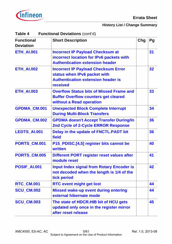
Table 4 Functional Deviations (cont’d)Functional Deviation
Short Description Chg Pg
Errata SheetHistory List / Change Summary
XMC4500, ES-AC, AC 5/61 Rel. 1.0, 2013-08Subject to Agreement on the Use of Product Information
ETH_AI.001 Incorrect IP Payload Checksum at incorrect location for IPv6 packets with Authentication extension header
31
ETH_AI.002 Incorrect IP Payload Checksum Error status when IPv6 packet with Authentication extension header is received
32
ETH_AI.003 Overflow Status bits of Missed Frame and Buffer Overflow counters get cleared without a Read operation
33
GPDMA_CM.001 Unexpected Block Complete Interrupt During Multi-Block Transfers
34
GPDMA_CM.002 GPDMA doesn't Accept Transfer During/In 2nd Cycle of 2-Cycle ERROR Response
36
LEDTS_AI.001 Delay in the update of FNCTL.PADT bit field
36
PORTS_CM.001 P15_PDISC.[4,5] register bits cannot be written
40
PORTS_CM.005 Different PORT register reset values after module reset
41
POSIF_AI.001 Input Index signal from Rotary Encoder is not decoded when the length is 1/4 of the tick period
42
RTC_CM.001 RTC event might get lost 44SCU_CM.002 Missed wake-up event during entering
external hibernate mode44
SCU_CM.003 The state of HDCR.HIB bit of HCU gets updated only once in the register mirror after reset release
45
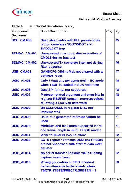
Table 4 Functional Deviations (cont’d)Functional Deviation
Short Description Chg Pg
Errata SheetHistory List / Change Summary
XMC4500, ES-AC, AC 6/61 Rel. 1.0, 2013-08Subject to Agreement on the Use of Product Information
SCU_CM.006 Deep sleep entry with PLL power-down option generates SOSCWDGT and SVCOLCKT trap
45
SDMMC_CM.001 Unexpected interrupts after execution of CMD13 during bus test
46
SDMMC_CM.002 Unexpected Tx complete interrupt during R1b response
46
USB_CM.002 GAHBCFG.GlblIntrMsk not cleared with a software reset
47
USIC_AI.005 Only 7 data bits are generated in IIC mode when TBUF is loaded in SDA hold time
48
USIC_AI.006 Dual SPI format not supported 48USIC_AI.007 Protocol-related argument and error bits in
register RBUFSR contain incorrect values following a received data word
48
USIC_AI.008 Bit SCLKOSEL in register BRG not implemented
50
USIC_AI.009 Baud rate generator interrupt cannot be used
51
USIC_AI.010 Minimum and maximum supported word and frame length in multi-IO SSC modes
51
USIC_AI.011 Write to TBUF01 has no effect 52USIC_AI.013 SCTR register bit fields DSM and HPCDIR
are not shadowed with start of data word transfer
52
USIC_AI.014 No serial transfer possible while running capture mode timer
52
USIC_AI.015 Wrong generation of FIFO standard transmit/receive buffer events when TBCTR.STBTEN/RBCTR.SRBTEN = 1
53
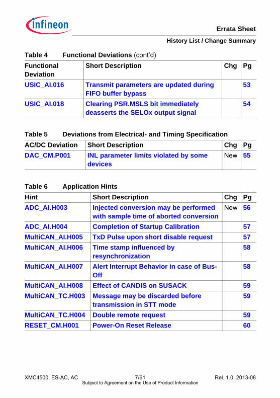
Table 4 Functional Deviations (cont’d)Functional Deviation
Short Description Chg Pg
Errata SheetHistory List / Change Summary
XMC4500, ES-AC, AC 7/61 Rel. 1.0, 2013-08Subject to Agreement on the Use of Product Information
USIC_AI.016 Transmit parameters are updated during FIFO buffer bypass
53
USIC_AI.018 Clearing PSR.MSLS bit immediately deasserts the SELOx output signal
54
Table 5 Deviations from Electrical- and Timing SpecificationAC/DC Deviation Short Description Chg PgDAC_CM.P001 INL parameter limits violated by some
devicesNew 55
Table 6 Application HintsHint Short Description Chg PgADC_AI.H003 Injected conversion may be performed
with sample time of aborted conversionNew 56
ADC_AI.H004 Completion of Startup Calibration 57MultiCAN_AI.H005 TxD Pulse upon short disable request 57MultiCAN_AI.H006 Time stamp influenced by
resynchronization58
MultiCAN_AI.H007 Alert Interrupt Behavior in case of Bus-Off
58
MultiCAN_AI.H008 Effect of CANDIS on SUSACK 59MultiCAN_TC.H003 Message may be discarded before
transmission in STT mode59
MultiCAN_TC.H004 Double remote request 59RESET_CM.H001 Power-On Reset Release 60
Table 4 Functional Deviations (cont’d)Functional Deviation
Short Description Chg Pg

Errata SheetFunctional Deviations
XMC4500, ES-AC, AC 8/61 Rel. 1.0, 2013-08Subject to Agreement on the Use of Product Information
2 Functional DeviationsThe errata in this section describe deviations from the documented functionalbehavior.
ADC_AI.008 Wait-for-Read condition for register GLOBRES not detectedin continuous auto-scan sequence
In the following scenario:• A continuous auto-scan is performed over several ADC groups and
channels by the Background Scan Source, using the global result register (GLOBRES) as result target (GxCHCTRy.RESTBS=1B), and
• The Wait-for-Read mode for GLOBRES is enabled (GLOBCR.WFR=1B), each conversion of the auto-scan sequence has to wait for its start until theresult of the previous conversion has been read out of GLOBRES. When the last channel of the auto-scan is converted and its result written toGLOBRES, the auto-scan re-starts with the highest channel number of thehighest ADC group number. But the start of this channel does not wait until theresult of the lowest channel of the previous sequence has been read fromregister GLOBRES, i.e. the result of the lowest channel may be lost.
WorkaroundIf either the last or the first channel in the auto-scan sequence does not write itsresult into GLOBRES, but instead into its group result register (selected via bitGxCHCTRy.RESTBS=0B), then the Wait-for-Read feature for GLOBRES workscorrectly for all other channels of the auto-scan sequence. For this purpose, the auto-scan sequence may be extended by a “dummy”conversion of group x/ channel y, where the Wait-for-Read mode must not beselected (GxRCRy.WFR=0B) if the result of this “dummy” conversion is notread.
Errata SheetFunctional Deviations
XMC4500, ES-AC, AC 9/61 Rel. 1.0, 2013-08Subject to Agreement on the Use of Product Information
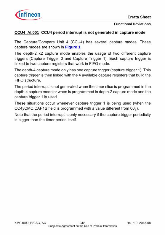
CCU4_AI.001 CCU4 period interrupt is not generated in capture mode
The Capture/Compare Unit 4 (CCU4) has several capture modes. Thesecapture modes are shown in Figure 1.The depth-2 x2 capture mode enables the usage of two different capturetriggers (Capture Trigger 0 and Capture Trigger 1). Each capture trigger islinked to two capture registers that work in FIFO mode.The depth-4 capture mode only has one capture trigger (capture trigger 1). Thiscapture trigger is then linked with the 4 available capture registers that build theFIFO structure.The period interrupt is not generated when the timer slice is programmed in thedepth-4 capture mode or when is programmed in depth-2 capture mode and thecapture trigger 1 is used.These situations occur whenever capture trigger 1 is being used (when theCC4yCMC.CAP1S field is programmed with a value different from 00B).Note that the period interrupt is only necessary if the capture trigger periodicityis bigger than the timer period itself.

Errata SheetFunctional Deviations
XMC4500, ES-AC, AC 10/61 Rel. 1.0, 2013-08Subject to Agreement on the Use of Product Information
Figure 1 CCU4 capture modes - a) Depth-2 x2 Capture; b) Depth-4 Capture
Workaround 1A straightforward workaround is to use only 2 capture registers (instead of amaximum of 4). This is done by setting the CC4yCMC.CAP1S to 00B andprogram the CC4yCMC.CAP0S with a value different from 00B.
Workaround 2By using the floating prescaler function present in each timer slice, the captureroutine can ignore the missing period interrupt, for a capture trigger frequencyas low as 0.25 Hz (for fCCU equal to 120 MHz).The floating prescaler function can be enabled by setting the CC4yTC.FPE =1B.
CC4yTIMER Capture register 3 Capture register 2 Capture register 1 Capture register 0
Capture trigger 1
08.03.2012 - 15.03.2012Depth-4 FIFO
CC4yTIMER
Capture register 3 Capture register 2
Capture register 1 Capture register 0
Capture trigger 1
08.03.2012 - 15.03.2012Depth-2 FIFO x 2
Capture trigger 0
a)
b)
Errata SheetFunctional Deviations
XMC4500, ES-AC, AC 11/61 Rel. 1.0, 2013-08Subject to Agreement on the Use of Product Information
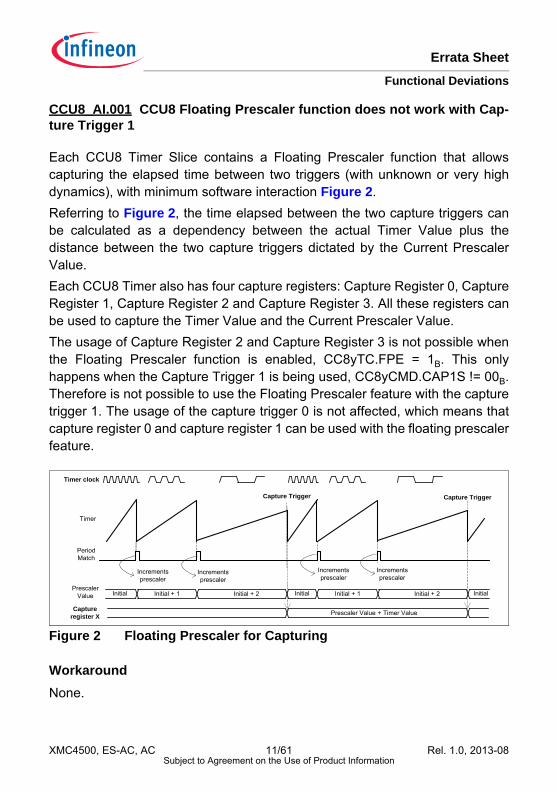
CCU8_AI.001 CCU8 Floating Prescaler function does not work with Cap-ture Trigger 1
Each CCU8 Timer Slice contains a Floating Prescaler function that allowscapturing the elapsed time between two triggers (with unknown or very highdynamics), with minimum software interaction Figure 2.Referring to Figure 2, the time elapsed between the two capture triggers canbe calculated as a dependency between the actual Timer Value plus thedistance between the two capture triggers dictated by the Current PrescalerValue.Each CCU8 Timer also has four capture registers: Capture Register 0, CaptureRegister 1, Capture Register 2 and Capture Register 3. All these registers canbe used to capture the Timer Value and the Current Prescaler Value.The usage of Capture Register 2 and Capture Register 3 is not possible whenthe Floating Prescaler function is enabled, CC8yTC.FPE = 1B. This onlyhappens when the Capture Trigger 1 is being used, CC8yCMD.CAP1S != 00B.Therefore is not possible to use the Floating Prescaler feature with the capturetrigger 1. The usage of the capture trigger 0 is not affected, which means thatcapture register 0 and capture register 1 can be used with the floating prescalerfeature.
Figure 2 Floating Prescaler for Capturing
WorkaroundNone.
Prescaler Value Initial Initial + 1
Timer clock
Initial + 2
Capture Trigger
Initial Initial + 1 Initial + 2 Initial
Timer
Capture Trigger
Period Match
Increments prescaler
Increments prescaler
Increments prescaler
Increments prescaler
Capture register X Prescaler Value + Timer Value
Errata SheetFunctional Deviations
XMC4500, ES-AC, AC 12/61 Rel. 1.0, 2013-08Subject to Agreement on the Use of Product Information
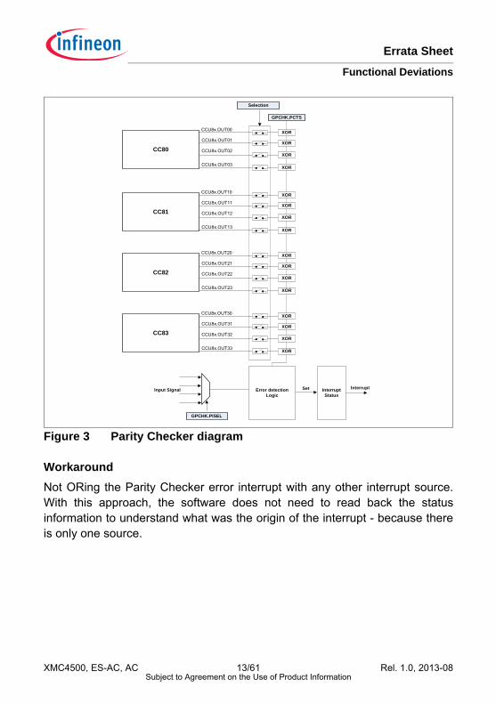
CCU8_AI.003 CCU8 Parity Checker Interrupt Status is cleared automati-cally by hardware
Each CCU8 Module Timer has an associated interrupt status register. ThisStatus register, CC8yINTS, keeps the information about which interrupt sourcetriggered an interrupt. The status of this interrupt source can only be cleared bysoftware. This is an advantage because the user can configure multipleinterrupt sources to the same interrupt line and in each triggered interruptroutine, it reads back the status register to know which was the origin of theinterrupt.Each CCU8 module also contains a function called Parity Checker. This ParityChecker function, crosschecks the output of a XOR structure versus an inputsignal, as seen in Figure 1.When using the parity checker function, the associated status bitfield, is clearedautomatically by hardware in the next PWM cycle whenever an error is notpresent.This means that if in the previous PWM cycle an error was detected and oneinterrupt was triggered, the software needs to read back the status registerbefore the end of the immediately next PWM cycle. This is indeed only necessary if multiple interrupt sources are ORed together inthe same interrupt line. If this is not the case and the parity checker error sourceis the only one associated with an interrupt line, then there is no need to readback the status information. This is due to the fact, that only one action can betriggered in the software routine, the one linked with the parity checker error.
Errata SheetFunctional Deviations
XMC4500, ES-AC, AC 13/61 Rel. 1.0, 2013-08Subject to Agreement on the Use of Product Information
Figure 3 Parity Checker diagram
WorkaroundNot ORing the Parity Checker error interrupt with any other interrupt source.With this approach, the software does not need to read back the statusinformation to understand what was the origin of the interrupt - because thereis only one source.
CCU8x.OUT00
CCU8x.OUT01
CCU8x.OUT02CC80
CCU8x.OUT03
CCU8x.OUT10
CCU8x.OUT11
CCU8x.OUT12CC81
CCU8x.OUT13
CCU8x.OUT20
CCU8x.OUT21
CCU8x.OUT22CC82
CCU8x.OUT23
CCU8x.OUT30
CCU8x.OUT31
CCU8x.OUT32CC83
CCU8x.OUT33
Input Signal
GPCHK.PISEL
GPCHK.PCTS
Set
Selection
XOR
XOR
XOR
XOR
XOR
XOR
XOR
XOR
XOR
XOR
XOR
XOR
XOR
XOR
XOR
XOR
Error detection Logic
Interrupt Status
Interrupt

Errata SheetFunctional Deviations
XMC4500, ES-AC, AC 14/61 Rel. 1.0, 2013-08Subject to Agreement on the Use of Product Information
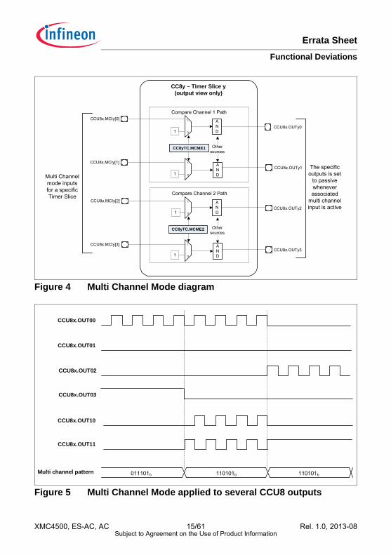
CCU8_AI.004 CCU8 output PWM glitch when using low side modulationvia the Multi Channel Mode
Each CCU8 Timer Slice can be configured to use the Multi Channel Mode - thisis done by setting the CC8yTC.MCME1 and/or CC8yTC.MCME2 bit fields to 1B.Each bit field enables the multi channel mode for the associated comparechannel of the CCU8 Timer Slice (each CCU8 Timer Slice has two comparechannels that are able to generate each a complementary pair of PWMoutputs).After enabled, the Multi Channel mode is then controlled by several inputsignals, one signal per output. Whenever an input is active, the specific PWMoutput is set to passive level - Figure 1.The Multi Channel mode is normally used to modulate in parallel several PWMoutputs (a complete CCU8 - up to 16 PWM signals can be modulated inparallel). A normal use case is the parallel control of the PWM output for BLDC motorcontrol. In Figure 2, we can see the Multi Channel Pattern being updatedsynchronously to the PWM signals. Whenever a multi channel input is active (inthis case 0), the specific output is set into passive level (the level in which theexternal switch is OFF).
Errata SheetFunctional Deviations
XMC4500, ES-AC, AC 15/61 Rel. 1.0, 2013-08Subject to Agreement on the Use of Product Information
Figure 4 Multi Channel Mode diagram
Figure 5 Multi Channel Mode applied to several CCU8 outputs
CC8y – Timer Slice y(output view only)
Compare Channel 1 Path
CCU8x.OUTy0AND
CC8yTC.MCME1
0
1
AND0
1
Other sources
CCU8x.MCIy[0]
CCU8x.MCIy[1]CCU8x.OUTy1
Compare Channel 2 Path
AND
CC8yTC.MCME2
0
1
AND0
1
Other sources
CCU8x.MCIy[2]
CCU8x.MCIy[3]
CCU8x.OUTy2
CCU8x.OUTy3
1
1
1
1
Multi Channel mode inputs for a specific Timer Slice
The specific outputs is set
to passive whenever associated
multi channel input is active
CCU8x.OUT00
CCU8x.OUT02
CCU8x.OUT10
Multi channel pattern 011101b 110101b 110101b
CCU8x.OUT01
CCU8x.OUT03
CCU8x.OUT11

Errata SheetFunctional Deviations
XMC4500, ES-AC, AC 16/61 Rel. 1.0, 2013-08Subject to Agreement on the Use of Product Information
A glitch is present at the PWM outputs whenever the dead time of the specificcompare channel is enabled - CC8yDTC.DTE1 and/or CC8yDTC.DTE2 set to1B (each compare channel has a separate dead time function) - and the specificmulti channel pattern for the channel is 01B or 10B.This glitch is not present if the specific timer slice is configure in symmetric edgealigned mode - CC8yTC.TCM = 0B and CC8yCHC.ASE = 0B.This glitch only affects the PWM output that is linked to the inverting ST path ofeach compare channel (non inverting outputs are not affected).The effect of this glitch can be seen in Figure 3. The duration of the PWM glitchhas the same length has the dead time value programmed into theCC8yDC1R.DT1F field (for compare channel 1) or into the CC8yDC1R.DT2F.
Figure 6 PWM output glitch
WorkaroundTo avoid the glitch on the inverting path of the PWM output, one can disable thedead time function before the Multi Channel Pattern is set to 01B or 10B.Disabling the dead time of the inverting PWM output can be done by setting: CC8yDTC.DCEN2 = 0 //if compare channel 1 is being used
CCU8x.OUT00
CCU8x.OUT02
CCU8x.OUT10
Multi channel pattern 011101b 110101b 110101b
CCU8x.OUT01
CCU8x.OUT03
CCU8x.OUT11

Errata SheetFunctional Deviations
XMC4500, ES-AC, AC 17/61 Rel. 1.0, 2013-08Subject to Agreement on the Use of Product Information
CC8yDTC.DCEN4 = 0 //if compare channel 2 is being used
The dead time needs to be re enabled, before the complementary outputsbecome modulated at the same time:CC8yDTC.DCEN2 = 1 //if compare channel 1 is being usedCC8yDTC.DCEN4 = 1 //if compare channel 2 is being used
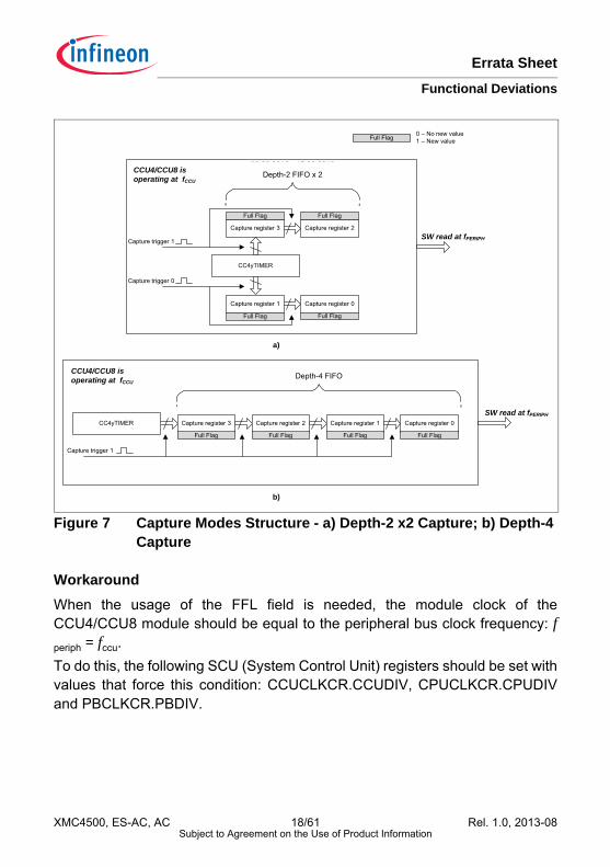
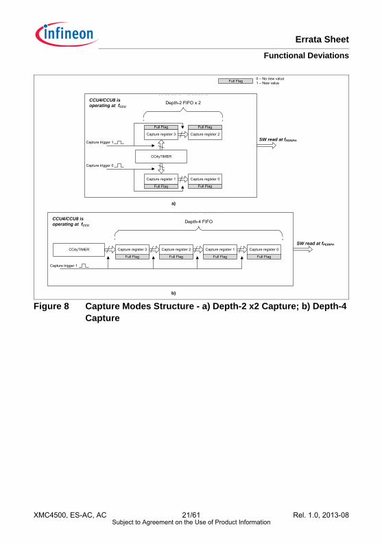
CCU_AI.001 CCU4 and CCU8 capture full flags do not work when moduleclock is faster than peripheral bus clock
Each CCU4/CCU8 timer slice contains a “Full Flag” field in every captureregister. The structure of the different capture modes for each timer slice can beseen in Figure 7.The full flag field serves as an indication to the software (when it is reading backthe specific capture register), for checking whether a new value has beencaptured or not into this register, since the previous read back.When the peripheral bus clock frequency is smaller than the CCU4/CCU8module clock frequency, fperiph < fccu, the read back of the full flag is inconsistent.Sometimes it returns the information that a new value has been captured andsometimes it does not.Note: The capture interrupt is generated correctly.
Errata SheetFunctional Deviations
XMC4500, ES-AC, AC 18/61 Rel. 1.0, 2013-08Subject to Agreement on the Use of Product Information
Figure 7 Capture Modes Structure - a) Depth-2 x2 Capture; b) Depth-4 Capture
WorkaroundWhen the usage of the FFL field is needed, the module clock of theCCU4/CCU8 module should be equal to the peripheral bus clock frequency: fperiph = fccu.To do this, the following SCU (System Control Unit) registers should be set withvalues that force this condition: CCUCLKCR.CCUDIV, CPUCLKCR.CPUDIVand PBCLKCR.PBDIV.
CC4yTIMER Capture register 3 Capture register 2 Capture register 1 Capture register 0
Capture trigger 1
08.03.2012 - 15.03.2012Depth-4 FIFO
CC4yTIMER
Capture register 3 Capture register 2
Capture register 1 Capture register 0
Capture trigger 1
08.03.2012 - 15.03.2012Depth-2 FIFO x 2
Capture trigger 0
a)
b)
Full Flag
Full Flag
Full Flag
Full Flag
Full Flag Full Flag Full Flag Full Flag
Full Flag 0 – No new value1 – New value
SW read at fPERIPH
SW read at fPERIPH
CCU4/CCU8 is operating at fCCU
CCU4/CCU8 is operating at fCCU
Errata SheetFunctional Deviations
XMC4500, ES-AC, AC 19/61 Rel. 1.0, 2013-08Subject to Agreement on the Use of Product Information
CCU_AI.002 CCU4 and CCU8 Prescaler synchronization clear does notwork when Module Clock is faster than Peripheral Bus Clock
Each CCU4/CCU8 module contains a feature that allows to clear the prescalerdivision counter synchronized with the clear of a run bit of a Timer Slice. This isconfigure via the GCTRL.PRBC field. The default value of 000B dictates thatonly the software can clear the prescaler internal division counter. Programminga value different from 000B into the PRBC will impose that the prescaler divisioncounter is cleared to 0D whenever the selected Timer Slice (selected via thePRBC field) run bit is cleared (TRB bit field).In normal operating conditions, clearing the internal prescaler division counteris not needed. The only situation were a clear of the division may be needed iswhen several Timer Slices inside one unit (CCU4/CCU8) are using differentprescaling factors and a realignment of all the timer clocks is needed. Thisnormally only has a benefit if there is a big difference between the prescalingvalues, e.g. Timer Slice 0 using a module clock divided by 2D and Timer Slice 1using a module clock divided by 1024D.When the peripheral bus clock frequency is smaller than the CCU4/CCU8module clock frequency, fperiph < fccu, it is not possible to clear the prescalerdivision counter, synchronized with the clear of the run bit of one specific TimerSlice.
Workaround 1The clearing of the prescaler internal division counter needs to be done viasoftware: GCTRL.PRBC programmed with 000B and whenever a clear isneeded, writing 1B into the GIDLS.CPRB bit field.
Workaround 2When the usage of the Prescaler internal division clear needs to besynchronized with a timer run bit clear, the module clock of the CCU4/CCU8should be equal to the peripheral bus clock frequency: fperiph = fccu.To do this, the following SCU (System Control Unit) registers should be set withvalues that force this condition: CCUCLKCR.CCUDIV, CPUCLKCR.CPUDIVand PBCLKCR.PBDIV.
Errata SheetFunctional Deviations
XMC4500, ES-AC, AC 20/61 Rel. 1.0, 2013-08Subject to Agreement on the Use of Product Information
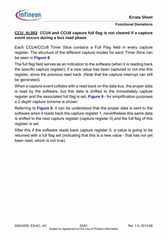
CCU_AI.003 CCU4 and CCU8 capture full flag is not cleared if a captureevent occurs during a bus read phase
Each CCU4/CCU8 Timer Slice contains a Full Flag field in every captureregister. The structure of the different capture modes for each Timer Slice canbe seen in Figure 8.The full flag field serves as an indication to the software (when it is reading backthe specific capture register), if a new value has been captured or not into thisregister, since the previous read back. (Note that the capture interrupt can stillbe generated).When a capture event collides with a read back on the data bus, the proper datais read by the software, but this data is shifted to the immediately captureregister and the associated full flag is set, Figure 9 - for simplification purposesa 2 depth capture scheme is shown.Referring to Figure 9, it can be understood that the proper data is sent to thesoftware when it reads back the capture register 1, nevertheless this same datais shifted to the next capture register (capture register 0) and the full flag of thisregister is set. After this if the software reads back capture register 0, a value is going to bereturned with a full flag set (indicating that this is a new value - that has not yetbeen read, which is not true).
Errata SheetFunctional Deviations
XMC4500, ES-AC, AC 21/61 Rel. 1.0, 2013-08Subject to Agreement on the Use of Product Information
Figure 8 Capture Modes Structure - a) Depth-2 x2 Capture; b) Depth-4 Capture
CC4yTIMER Capture register 3 Capture register 2 Capture register 1 Capture register 0
Capture trigger 1
08.03.2012 - 15.03.2012Depth-4 FIFO
CC4yTIMER
Capture register 3 Capture register 2
Capture register 1 Capture register 0
Capture trigger 1
08.03.2012 - 15.03.2012Depth-2 FIFO x 2
Capture trigger 0
a)
b)
Full Flag
Full Flag
Full Flag
Full Flag
Full Flag Full Flag Full Flag Full Flag
Full Flag 0 – No new value1 – New value
SW read at fPERIPH
SW read at fPERIPH
CCU4/CCU8 is operating at fCCU
CCU4/CCU8 is operating at fCCU

Errata SheetFunctional Deviations
XMC4500, ES-AC, AC 22/61 Rel. 1.0, 2013-08Subject to Agreement on the Use of Product Information
Figure 9 Capture shift during read back phase - a) Capture trigger without collision with read back; b) Capture trigger collision with read back
Workaround 1If the dynamics of the capture trigger(s) cannot guarantee a safe read back ofthe captured data without collision, then the software can monitor if the timerhas rollover or not between two reads.This can be done by enabling per example by setting the timer mode in EdgeAligned, TCM = 0B and enabling the Period Interrupt PME = 1B. This interruptshould then be routed to one of the service request outputs by setting the POSRfield accordingly (e.g. setting POSR = 00B will output the Period Interrupt at theService Request Output 0 of CCU4/CCU8).
056FH
056FH Empty
Capture trigger
24.07.2012 - 31.07.2012Depth-2 FIFO x 2
a)
Full Flag = 0Full Flag = 1
Full Flag 0 – No new value1 – New value
Timeframe 0
SW read at fPERIPH from Capture Register 1
F960H
F960H 056FH
Capture trigger
24.07.2012 - 31.07.2012Depth-2 FIFO x 2
b)
Full Flag = 1Full Flag = 1
Timeframe 1
Capture register 1 Capture register 0
Capture register 1 Capture register 0
Timer
Timer
HW returns:Full Flag = 1 and F960H

Errata SheetFunctional Deviations
XMC4500, ES-AC, AC 23/61 Rel. 1.0, 2013-08Subject to Agreement on the Use of Product Information
In every read back where the software finds a value equal to the previous one,it should then poll the interrupt status to understand if the timer has rollover ornot. If the timer has not rollover, then this is the same value that was previouslyread.
Workaround 2The software reads back in every capture event. This can be done by enablingthe capture interrupt, and in each capture interrupt it reads back a captureregister.Enabling the capture interrupt is done in the following way: if the capture triggeris linked to input Event 0, then E0AE needs to be set to 1B; if the capture triggeris linked to input Event 1, then E1AE needs to be set to 1B; if the capture triggeris linked to input Event 2, then E2AE needs to be set to 1B.Routing the interrupt to one of the four available service request outputs: ifEvent 0 is being used and the Service Request Output 0 should be used, thenE0SR needs to be set with the value 00B (for Event 1 the field is E1SR and forEvent 2 E2SR).
CCU_AI.004 CCU4 and CCU8 Extended Read Back loss of data
Each CCU4/CCU8 Timer Slice contains a bit field that allows the enabling of theExtended Read Back feature. This is done by setting theCC8yTC.ECM/CC4yTC.ECM = 1B. Setting this bit field to 1B only has an impactif the specific Timer Slice is working in Capture Mode (CC8yCMC.CAP1S orCC8yCMC.CAP0S different from 00B - same fields for CCU4).By setting the bit field to ECM = 1B, is then possible to read back the capturedata of the specific Timer Slice (or multiple Timer Slices, if this bit field is set inmore than one Timer Slice) trough a single address. This address is linked tothe ECRD register.Referring to Figure 10, the hardware every time that the software reads backfrom the ECRD address, will return the immediately next capture register thatcontains new data. This is done in a circular access, that contains all the captureregisters from the Timer Slices that are working in capture mode.

Errata SheetFunctional Deviations
XMC4500, ES-AC, AC 24/61 Rel. 1.0, 2013-08Subject to Agreement on the Use of Product Information
When using this feature, there is the possibility of losing captured data within aTimer Slice. The data that is lost is always the last captured data within a timerslice, e.g (with CCU4 nomenclature - same applies to CCU8):• Timer X has 4 capture registers and is the only Timer set with ECM = 1B. At
the moment that the software starts reading the capture registers via the ECRD address, we have already capture four values. The ECRD read back will output CC4xC0V -> CC4xC1V -> CC4xC2V -> CC4xC2V (CC4xC3V value is lost)
• Timer X has 4 capture registers and is the only Timer set with ECM = 1B. At the moment that the software starts reading the capture registers via the ECRD address, we have already capture two values. The ECRD read back will output CC4xC2V -> CC4xC2V (CC4xC3V value is lost)
• Timer X and Timer Y have 4 capture registers each and they are both configured with ECM = 1B. At the moment that the software starts reading the capture registers via the ECRD address, we have already capture two values on Timer X and 4 on Timer Y. The ECRD read back will output CC4xC0V -> CC4xC1V -> CC4xC2V -> CC4xC3V -> CC4yC2V -> CC4yC2V (CC4yC3V value is lost)
Figure 10 Extended Read Back access - example for CCU4 (CCU8 structure is the same)
Timer Slice 3
Timer Slice 2
Timer Slice 1
Timer Slice 0CC40C0Vptr stays if
full
CC40C1Vptr stays if
full
CC40C2Vptr stays if
full
CC40C3Vptr stays if
full
CC41C0Vptr stays if
full
CC41C1Vptr stays if
full
CC41C2Vptr stays if
full
CC41C3Vptr stays if
full
ptr ptr ptr
ptr
ptr ptr ptr
CC42C0Vptr stays if
full
CC42C1Vptr stays if
full
CC42C2Vptr stays if
full
CC42C3Vptr stays if
full
CC43C0Vptr stays if
full
CC43C1Vptr stays if
full
CC43C2Vptr stays if
full
CC43C3Vptr stays if
full
ptr ptr ptr
ptr
ptr ptr ptr
ptr
ptr
SW reads from ECRD address and HW goes through all capture registers (in a circular way) and returns the capture register that contains new data
Errata SheetFunctional Deviations
XMC4500, ES-AC, AC 25/61 Rel. 1.0, 2013-08Subject to Agreement on the Use of Product Information
WorkaroundNone.
CCU_AI.005 CCU4 and CCU8 External IP clock Usage
Each CCU4/CCU8 module offers the possibility of selecting an external signalto be used as the master clock for every timer inside the module Figure 1.External signal in this context is understood as a signal connected to othermodule/IP or connected to the device ports.The user has the possibility after selecting what is the clock for the module(external signal or the clock provided by the system), to also select if this clockneeds to be divided. The division ratios start from 1 (no frequency division) upto 32768 (where the selected timer uses a frequency of the selected clockdivided by 32768).This division is selected by the PSIV field inside of the CC4yPSC/CC8yPSCregister. Notice that each Timer Slice (CC4y/CC8y) have a specific PSIV field,which means that each timer can operate in a different frequency.Currently is only possible to use an external signal as Timer Clock when adivision ratio of 2 or higher is selected. When no division is selected (divided by1), the external signal cannot be used.The user must program the PSIV field of each Timer Slice with a value differentfrom 0000B - minimum division value is /2.This is only applicable if the Module Clock provided by the system (the normaldefault configuration and use case scenario) is not being used. In the case thatthe normal clock configured and programmed at system level is being used,there is not any type of constraints.One should not also confuse the usage of an external signal as clock for themodule with the usage of an external signal for counting. These two featuresare completely unrelated and there are not any dependencies between both.

Errata SheetFunctional Deviations
XMC4500, ES-AC, AC 26/61 Rel. 1.0, 2013-08Subject to Agreement on the Use of Product Information
Figure 11 Clock Selection Diagram for CCU4/CCU8
WorkaroundNone.
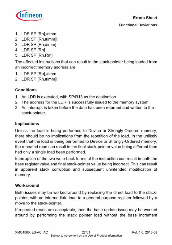
CPU_CM.001 Interrupted loads to SP can cause erroneous behavior
If an interrupt occurs during the data-phase of a single word load to the stack-pointer (SP/R13), erroneous behavior can occur. In all cases, returning from theinterrupt will result in the load instruction being executed an additional time. Forall instructions performing an update to the base register, the base register willbe erroneously updated on each execution, resulting in the stack-pointer beingloaded from an incorrect memory location.The affected instructions that canresult in the load transaction being repeated are:
CCU4/CCU8
CC40/CC80
... ... Timer clock
CC41/CC81
... Timer clock
CC42/CC82
... Timer clock
CC43/CC83
... Timer clock
Module clock from the system
Mod
ule
Exte
rnal
Si
gnal
s
Prescaler
/1/2
/16384/32768
CC4/80PSC.PSIV
CC4/81PSC.PSIV
CC4/82PSC.PSIV
CC4/83PSC.PSIV
Errata SheetFunctional Deviations
XMC4500, ES-AC, AC 27/61 Rel. 1.0, 2013-08Subject to Agreement on the Use of Product Information
1. LDR SP,[Rn],#imm2. LDR SP,[Rn,#imm]!3. LDR SP,[Rn,#imm]4. LDR SP,[Rn]5. LDR SP,[Rn,Rm]The affected instructions that can result in the stack-pointer being loaded froman incorrect memory address are:1. LDR SP,[Rn],#imm2. LDR SP,[Rn,#imm]!
Conditions1. An LDR is executed, with SP/R13 as the destination2. The address for the LDR is successfully issued to the memory system3. An interrupt is taken before the data has been returned and written to the
stack-pointer.
ImplicationsUnless the load is being performed to Device or Strongly-Ordered memory,there should be no implications from the repetition of the load. In the unlikelyevent that the load is being performed to Device or Strongly-Ordered memory,the repeated read can result in the final stack-pointer value being different thanhad only a single load been performed.Interruption of the two write-back forms of the instruction can result in both thebase register value and final stack-pointer value being incorrect. This can resultin apparent stack corruption and subsequent unintended modification ofmemory.
WorkaroundBoth issues may be worked around by replacing the direct load to the stack-pointer, with an intermediate load to a general-purpose register followed by amove to the stack-pointer.If repeated reads are acceptable, then the base-update issue may be workedaround by performing the stack pointer load without the base increment

Errata SheetFunctional Deviations
XMC4500, ES-AC, AC 28/61 Rel. 1.0, 2013-08Subject to Agreement on the Use of Product Information
followed by a subsequent ADD or SUB instruction to perform the appropriateupdate to the base register.
CPU_CM.004 VDIV or VSQRT instructions might not complete correctlywhen very short ISRs are used
The VDIV and VSQRT instructions take 14 cycles to execute. When an interruptis taken a VDIV or VSQRT instruction is not terminated, and completes itsexecution while the interrupt stacking occurs. If lazy context save of floatingpoint state is enabled then the automatic stacking of the floating point contextdoes not occur until a floating point instruction is executed inside the interruptservice routine.Lazy context save is enabled by default. When it is enabled, the minimum timefor the first instruction in the interrupt service routine to start executing is 12cycles. In certain timing conditions, and if there is only one or two instructionsinside the interrupt service routine, then the VDIV or VSQRT instruction mightnot write its result to the register bank or to the FPSCR.
Conditions1. The floating point unit is present and enabled2. Lazy context saving is not disabled3. A VDIV or VSQRT is executed4. The destination register for the VDIV or VSQRT is one of s0 - s155. An interrupt occurs and is taken6. The interrupt service routine being executed does not contain a floating
point instruction7. 14 cycles after the VDIV or VSQRT is executed, an interrupt return is
executedA minimum of 12 of these 14 cycles are utilized for the context state stacking,which leaves 2 cycles for instructions inside the interrupt service routine, or 2wait states applied to the entire stacking sequence (which means that it is not aconstant wait state for every access).In general this means that if the memorysystem inserts wait states for stack transactions then this erratum cannot beobserved.
Errata SheetFunctional Deviations
XMC4500, ES-AC, AC 29/61 Rel. 1.0, 2013-08Subject to Agreement on the Use of Product Information
ImplicationsThe VDIV or VQSRT instruction does not complete correctly and the registerbank and FPSCR are not updated, meaning that these registers hold incorrect,out of date, data.
WorkaroundA workaround is only required if the floating point unit is present and enabled.A workaround is not required if the memory system inserts one or more waitstates to every stack transaction.There are two workarounds:1. Disable lazy context save of floating point state by clearing LSPEN to 0 (bit
30 of the FPCCR at address 0xE000EF34).2. Ensure that every interrupt service routine contains more than 2 instructions
in addition to the exception return instruction.
DAC_CM.001 DAC immediate register read following a write issue
In case a read access to a DAC register is done immediately after a writeaccess to the same register, the `old` data value is returned, which was storedbefore the write access, and not the newly written one.
WorkaroundIn case of a series of write accesses to DAC registers, repeat the last writeaccess. In case of a single write access, repeat this one. Then no read accesscan fail.
DAC_CM.002 No error response for write access to read only DAC ID reg-ister
The DAC ID register is a read only register. But in case a write access is doneto it, no bus error response is returned. The DAC ID register value is kept, asintended.
Errata SheetFunctional Deviations
XMC4500, ES-AC, AC 30/61 Rel. 1.0, 2013-08Subject to Agreement on the Use of Product Information
WorkaroundNone.
DEBUG_CM.001 OCDS logic in peripherals affected by TRST
The OCDS logic in peripherals is erroneously reset if TRST is activated.In the device the OCDS logic in the peripherals is kept in reset and therefore notavailable by default (after reset) because P0.8 is configured as TRST and theinternal pull-down is active.
Workaround 1Connect an external pull-up resistor to P0.8 to drive TRST high (inactive), ifP0.8 is not used by the application.
Workaround 2During software configuration program P0.8 as GPIO input, This configurationdrives TRST internally to the inactive state.Note: With this solution the debug functionality remains unavailable right after
reset.
DEBUG_CM.002 CoreSight logic only reset after power-on reset
The CoreSight logic should also be reset with a debug reset (DBGRESET).Opposed to this specification the debug reset does not have an effect on theCoreSight logic. Therefore CoreSight logic can only be reset by a power-onreset (PORESET).
WorkaroundIf the user quits the debug session and likes to leave the system clean, withouta PORESET, the following steps have to be performed:• Disable debug functions by disable of DHCSR.C_DEBUGEN bit in debug
halting and status register.
Errata SheetFunctional Deviations
XMC4500, ES-AC, AC 31/61 Rel. 1.0, 2013-08Subject to Agreement on the Use of Product Information
• Disable HW breakpoints in FPB unit of each comparator by disable of FP_CTRL.ENABLE bit in flashpatch control register.
• Disable trace functions by disable of DEMCR.TRCENA bit in debug exception and monitor control register. This disables DWT, ITM, ETM and TPIU functions.
ETH_AI.001 Incorrect IP Payload Checksum at incorrect location for IPv6packets with Authentication extension header
When enabled, the Ethernet MAC computes and inserts the IP headerchecksum (IPv4) or TCP, UDP, or ICMP payload checksum in the transmittedIP datagram (IPv4 or IPv6) on per-packet basis. The Ethernet MAC processesthe IPv6 header and the optional extension headers (if present) to identify thestart of actual TCP, UDP, or ICMP payload for correct computation andinsertion of payload checksum at appropriate location in the packet. The IPv6header length is fixed (40 bytes) whereas the extension header length isspecified in units of N bytes:Extension Header Length Field Value x N bytes + 8 bytes where N = 4 for authentication extension header and N = 8 for all otherextension headers supported by the Ethernet MAC. If the actual payload bytesare less than the bytes indicated in the Payload Length field of the IP header,the Ethernet MAC indicates the IP Payload Checksum error.If the payload checksum is enabled for an IPv6 packet containing theauthentication extension header, then instead of bypassing the payloadchecksum insertion, the Ethernet MAC incorrectly processes the packet andinserts a payload checksum at an incorrect location. As a result, the packet getscorrupted, and it is dropped at the destination. The software should not enablethe payload checksum insertion for such packets because the Integrity CheckValue (ICV) in the authentication extension header is calculated and insertedconsidering that the payload data is immutable (not modified) in transit.Therefore, even if the payload checksum is correctly calculated and inserted, itresults into a failure of the ICV check at the final destination and the packet iseventually dropped.
Errata SheetFunctional Deviations
XMC4500, ES-AC, AC 32/61 Rel. 1.0, 2013-08Subject to Agreement on the Use of Product Information
WorkaroundThe software should not enable the IP payload checksum insertion by theEthernet MAC for Tx IPv6 packets with authentication extension headers. Thesoftware can compute and insert the IP payload checksum for such packets.
ETH_AI.002 Incorrect IP Payload Checksum Error status when IPv6 pack-et with Authentication extension header is received
The Ethernet MAC processes a TCP, UDP, or ICMP payload in the received IPdatagrams (IPv4 or IPv6) and checks whether the received checksum fieldmatches the computed value. The result of this operation is given as an IPPayload Checksum Error in the receive status word. This status bit is also set ifthe length of the TCP, UDP, or ICMP payload does not match the expectedpayload length given in the IP header.In IPv6 packets, there can be optional extension headers before actual TCP,UDP, or ICMP payload. To compute and compare the payload checksum forsuch packets, the Ethernet MAC sequentially parses the extension headers,determines the extension header length, and identifies the start of actual TCP,UDP, or ICMP payload. The header length of all extension headers supportedby the Ethernet MAC is specified in units of 8 bytes (Extension Header LengthField Value x 8 bytes + 8 bytes) except in the case of authentication extensionheader. For authentication extension header, the header length is specified inunits of 4 bytes (Extension Header Length Field Value x 4 bytes + 8 bytes).However, because of this defect, the Ethernet MAC incorrectly interprets thesize of the authentication extension header in units of 8 bytes, because of whichthe following happens:• Incorrect identification of the start of actual TCP, UDP, or ICMP payload• Computing of incorrect payload checksum• Comparison with incorrect payload checksum field in the received IPv6
frame that contains the authentication extension header• Incorrect IP Payload Checksum Error statusAs a result, the IP Payload checksum error status is generated for proper IPv6packets with authentication extension header. If the Ethernet MAC core is
Errata SheetFunctional Deviations
XMC4500, ES-AC, AC 33/61 Rel. 1.0, 2013-08Subject to Agreement on the Use of Product Information
programmed to drop such `error` packets, such packets are not forwarded tothe host software stack.
WorkaroundDisable dropping of TCP/IP Checksum Error Frames by setting Bit 26 (DT) inthe Operation Mode Register (OPERATION_MODE). This enables the EthernetMAC core to forward all packets with IP checksum error to the software driver.The software driver must process all such IPv6 packets that have payloadchecksum error status and check whether they contain the authenticationextension header. If authentication extension header is present, the softwaredriver should either check the payload checksum or inform the upper softwarestack to check the packet for payload checksum.
ETH_AI.003 Overflow Status bits of Missed Frame and Buffer Overflowcounters get cleared without a Read operation
The DMA maintains two counters to track the number of frames missedbecause of the following:• Rx Descriptor not being available• Rx FIFO overflow during receptionThe Missed Frame and Buffer Overflow Counter register indicates the currentvalue of the missed frames and FIFO overflow frame counters. This registeralso has the Overflow status bits (Bit 16 and Bit 28) which indicate whether therollover occurred for respective counter. These bits are set when respectivecounter rolls over. These bits should remain high until this register is read. However, erroneously, when the counter rollover occurs second time after thestatus bit is set, the respective status bit is reset to zero.
EffectsThe application may incorrectly detect that the rollover did not occur since thelast read operation.

Errata SheetFunctional Deviations
XMC4500, ES-AC, AC 34/61 Rel. 1.0, 2013-08Subject to Agreement on the Use of Product Information
WorkaroundThe application should read the Missed Frame and Buffer Overflow Counterregister periodically (or after the Overflow or Rollover status bits are set) suchthat the counter rollover does not occur twice between read operations.
GPDMA_CM.001 Unexpected Block Complete Interrupt During Multi-Block Transfers
The GPMDA allows an interrupt to be generated on completion of a DMA blocktransfer to the destination. This interrupt is generated if the INT_EN (CTLx[0])bit is set. On a channel enabled for multi-block transfers, the CTLx register isreprogrammed using either of the following methods: • Block chaining using linked lists• Auto-reloadingWhen CTLx is re-programmed using block-chaining of linked lists, interruptscan be enabled or disabled seperately for each block in the transfer. The blockinterrupt is generated from a combinational logic, which is coded such that, fora particular channel, if the 'RawBlock' register bit is set and the rawblockinterrupt is unmasked, an interrupt is triggered soon as the INT_EN (CTLx[0])bit is written as `1`, as shown in the equation below:block_int = rawblock & (!maskblock) & int_en ;
This can cause a false block interrupt to be generated in multi-block transfers.
Conditions1. Consider a multi-block transfer of three blocks(LLI0, LLI1, LLI2) on
channelX, where SARx, DARx, CTLx are all re-programmed using linked lists.
2. For the first block, interrupts are not enabled; that is, LLI0.CTLx[0] = 0. For the second and third blocks, interrupts are enabled; that is, LLI1.CTLx[0] = 1, LLI2.CTLx[0] = 1.
3. Block interrupt for channel x is unmasked by writing to MaskBlock register.4. After the first block transfer completes, the rawblock bit is set to 1; that is,
RawBlock[0] = 1. At this point, no interrupt is generated because, for this block, int_en = 0; that is, LLI0.CTLx[0] = 0 ).

Errata SheetFunctional Deviations
XMC4500, ES-AC, AC 35/61 Rel. 1.0, 2013-08Subject to Agreement on the Use of Product Information
5. An LLI update occurs for the next block transfer, and SARx, DARx, and CTLx are re-programmed with the contents of LLI1.SARx, LL1.DARx, and LLI1.CTLx, respectively.
6. Since the RawBlock register has not been cleared by software after the first block completion, RawBlock[0] is still set to 1.
7. Because LLI1.CTLx[0] = 1, the int_en bit is set to `1` as soon as CTLx is updated with the contents of LLI1.CTLx[0]. This triggers a false Block Complete Interrupt at this point.
ImplicationsUnexpected Block Complete Interrupt can occur during Multi-Block Transfers.
WorkaroundThe software knows which blocks of the multi-block transfer are interrupt-enabled. Based on this, code the Interrupt Service Routine such that it keeps acount of the interrupts. It can then ignore the unwanted interrupts and serviceonly the expected interrupts.In the example above, the software expects blockinterrupts only for LLI1 and LLI2, but not for LLI0. So the ISR can be coded toignore the first interrupt and service the next two interrupts, as shown in thepsuedo code below: ISR : blk_flag++ If(blk_flag==1) { clear_block_interrupt exit } else { // do normal operation; }
Errata SheetFunctional Deviations
XMC4500, ES-AC, AC 36/61 Rel. 1.0, 2013-08Subject to Agreement on the Use of Product Information
GPDMA_CM.002 GPDMA doesn't Accept Transfer During/In 2nd Cycle of2-Cycle ERROR Response
In the GPDMA, the slave bus interface unit is coded such that, after the secondcycle of a two-cycle error response, the logic transitions the state machine tothe IDLE state and hence does not accept any transfer issued during thesecond cycle of the two-cycle error response.
Workaround• Write software to not perform any actions that cause GPDMA to generate
an error response.• Ensure that any master that communicates to the GPDMA does not issue a
transfer in the second cycle of a two-cycle error response.
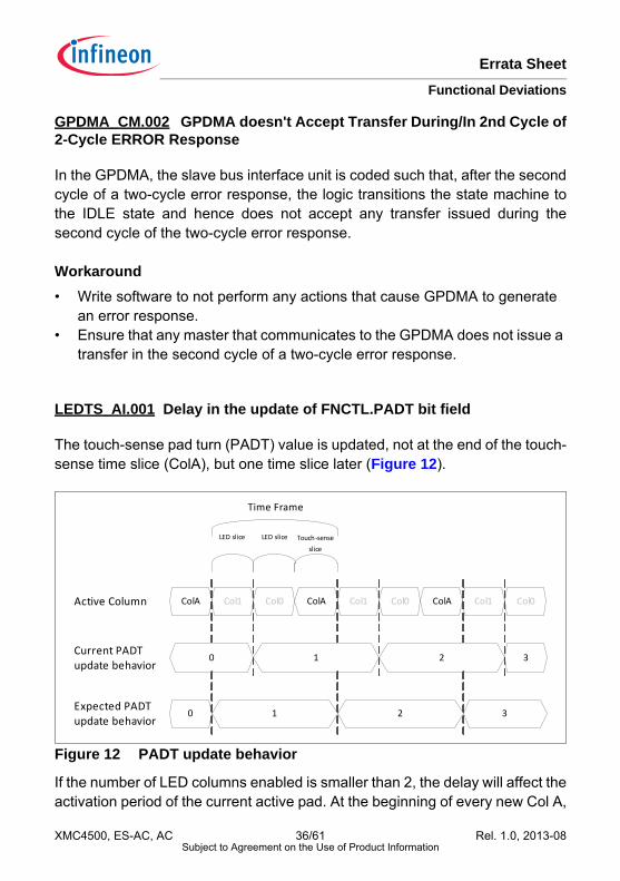
LEDTS_AI.001 Delay in the update of FNCTL.PADT bit field
The touch-sense pad turn (PADT) value is updated, not at the end of the touch-sense time slice (ColA), but one time slice later (Figure 12).
Figure 12 PADT update behavior
If the number of LED columns enabled is smaller than 2, the delay will affect theactivation period of the current active pad. At the beginning of every new Col A,
Active Column Col1 Col0 ColA Col1 Col0 Col1 Col0ColAColA
0 1 2 3
0 1 2 3
Current PADT update behavior
Expected PADT update behavior
Time Frame
LED slice Touch ‐sense slice
LED slice
Errata SheetFunctional Deviations
XMC4500, ES-AC, AC 37/61 Rel. 1.0, 2013-08Subject to Agreement on the Use of Product Information
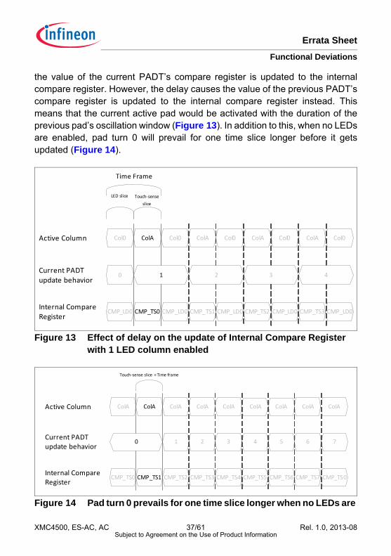
the value of the current PADT’s compare register is updated to the internalcompare register. However, the delay causes the value of the previous PADT’scompare register is updated to the internal compare register instead. Thismeans that the current active pad would be activated with the duration of theprevious pad’s oscillation window (Figure 13). In addition to this, when no LEDsare enabled, pad turn 0 will prevail for one time slice longer before it getsupdated (Figure 14).
Figure 13 Effect of delay on the update of Internal Compare Register with 1 LED column enabled
Figure 14 Pad turn 0 prevails for one time slice longer when no LEDs are
Active Column ColA Col0 ColA Col0 ColA ColA Col0Col0Col0
1 2 3Current PADT update behavior
40
CMP_TS0CMP_LD0Internal Compare Register
CMP_TS1CMP_LD0 CMP_TS2CMP_LD0 CMP_TS3CMP_LD0 CMP_LD0
Time Frame
LED slice Touch‐sense slice
Active Column ColA ColA ColA ColA ColA ColA ColAColAColA
0 1 3Current PADT update behavior
5 7
CMP_TS1CMP_TS0Internal Compare Register
CMP_TS3CMP_TS2 CMP_TS5CMP_TS4 CMP_TS7CMP_TS6 CMP_TS0
2 4 6
Touch ‐sense slice = Time frame

Errata SheetFunctional Deviations
XMC4500, ES-AC, AC 38/61 Rel. 1.0, 2013-08Subject to Agreement on the Use of Product Information
enabled
If the number of LED columns enabled is 2 or more, the additional LED columnswould provide some buffer time for the delay. So, at the start of a new touch-sense time slice, the update of PADT value would have taken place. Hence, thecurrent active PADT compare register value is updated to the internal compareregister (Figure 15).
Figure 15 Internal Compare Register updated with correct compare register value with 2 LED columns enabled
ConditionsThis delay in PADT update can be seen in cases where hardware pad turncontrol mode (FNCTL.PADTSW = 0) is selected and the touch-sense functionis enabled (GLOBCTL.TS_EN = 1).
WorkaroundThis section is divided to two parts. The first part will provide a guide on readingthe value of the bit field FNCTL.PADT via software. The second part will providesome workarounds for ensuring that the CMP_TS[x] values are aligned to thecurrent active pad turn.
Active Column Col1 Col0 ColA Col1 Col0 Col1 Col0ColAColA
0 1 2 3Current PADT update behavior
CMP_LD1CMP_TS0Internal Compare Register
CMP_TS1CMP_LD0 CMP_LD0CMP_LD1 CMP_LD1CMP_TS2 CMP_LD0
Time Frame
LED slice Touch ‐sense slice
LED slice
Errata SheetFunctional Deviations
XMC4500, ES-AC, AC 39/61 Rel. 1.0, 2013-08Subject to Agreement on the Use of Product Information
Workaround for reading PADTDue to the delay in the PADT update, the user would get the current active padturn when PADT is read in the time frame interrupt. However, this PADT valueread differs when read in a time slice interrupt. This depends on the number ofLED columns enabled and the active function or LED column in the previoustime slice (Table 7). The bit field FNCTL.FNCOL provides a way of interpretingthe active function or LED column in the previous time slice.
Workaround for aligning CMP_TSxOne workaround is to use the software pad turn control. Then this issue can beavoided entirely because the pad turn update will have to be handled bysoftware.However, it is still possible to work around this issue when using the hardwarepad turn control. In the previous section, it is known that when the number ofLED columns enabled is smaller than 2, the current active pad is activated withthe oscillation window of the previous active pad. This means that the currentactive pad is activated with the value programmed in the bit field CMP_TS[x-1]instead of CMP_TS[x]. There are two possible software workarounds for thisissue:
Table 7 PADT value as read in the time slice interruptNo. of LED Columns Enabled
Previous active function / LED column
FNCTL.FNCOL PADT value
0-1 Touch-sense or LED Col0
110B or 111B Previous active pad turn
2-7 Touch-sense or first LED column after touch-sense
110B or 111B Previous active pad turn
Second LED column after touch-sense onwards
101B to 000B Current or next active pad turn

Errata SheetFunctional Deviations
XMC4500, ES-AC, AC 40/61 Rel. 1.0, 2013-08Subject to Agreement on the Use of Product Information
1. At the end of the time frame interrupt service routine, software can prepare for the next active pad turn by programming the CMP_TS[x-1] bit field with the intended compare value for TSIN[x]. As an example, if the next active pad is TSIN[2], program CMP_TS[1] with the compare value intended for TSIN[2] (Figure 16).
Figure 16 Software workaround demonstration
1. During the initialization phase, program the CMP_TS[x] bit fields with the left-shift factored in. Example: CMP_TS[0] for TSIN[1], CMP_TS[1] for TSIN[2], ... CMP[7] for TSIN[0].
PORTS_CM.001 P15_PDISC.[4,5] register bits cannot be written
The bits 4 and 5 of the register P15_PDISC cannot be modified by software andalways retain their reset value 0B. As a result of this, the digital input path of therelated shared analog and digital input pins cannot be disabled.
ImplicationsSoftware that sets one or both of these bits and later reads P15_PDISC will notsee the expected read value, but always reads 0B for P15_PDISC.[4,5].Software that reads P15_IN will read undefined values for P15_IN[4,5]. Theread values depend on the analog input level of the respective pin.
WorkaroundNone.
Active Column ColA Col0 ColA Col0 ColA ColA Col0Col0Col0
1 2 3PADT value read 40
Time Frame
Time Frame InterruptNext active pad = TSIN[2]Program CMP_TS1 with
value intended for TSIN[2]
Time Frame InterruptNext active pad = TSIN[3]Program CMP_TS2 with
value intended for TSIN[3]
Time Frame InterruptNext active pad = TSIN[4]Program CMP_TS3 with value intended for TSIN[4]
Time Frame InterruptNext active pad = TSIN[5]Program CMP_TS4 with value intended for TSIN[5]

Errata SheetFunctional Deviations
XMC4500, ES-AC, AC 41/61 Rel. 1.0, 2013-08Subject to Agreement on the Use of Product Information
PORTS_CM.005 Different PORT register reset values after module reset
The PORTS registers can be reset independent of the reset of the system withSCU_PRSET1.PPORTSRS. After such a module reset, some PORTS registershave a reset value different to the reset value that is documented in theReference Manual.
ImplicationsThe different value in Pn_IOCR8 configures the respective port pins Pn.[11:8]as inverted inputs instead of direct inputs. User software in Priviledged Modecan reconfigure them as needed by the application.With the different value in Pn_PDISC of the digital ports the availability of digitalpins in a device can no longer be verified via this register. Note that Pn_PDISCof pure digital ports is read-only; user software can’t write to them.The Pn_PDISC of the shared analog/digital port pins (P14 and P15)enables/disables the digital input path. After a system reset this path isdisabled, after a module reset enabled. User software in Priviledged Mode canreconfigure them as needed by the application.The different value in the Pn_PDR registers configures output port pins with a“Strong-Sharp” output driver mode, as opposed to “Strong-Soft” driver modeafter a system reset. This may result in a higher current consumption and morenoise induced to the external system. User software in Priviledged Mode canreconfigure them as needed by the application.
Table 8 PORTS registers reset valuesRegister Sytem reset value Module reset valuePn_IOCR8 0000 0000H 2020 2020H
1)
1) Only in XMC4500 devices.
Pn_PDISC XXXX XXXXH2)
2) Device and package dependent
0000 0000H
Pn_PDR0 2222 2222H 0000 0000H
Pn_PDR1 2222 2222H 0000 0000H

Errata SheetFunctional Deviations
XMC4500, ES-AC, AC 42/61 Rel. 1.0, 2013-08Subject to Agreement on the Use of Product Information
WorkaroundNone.
POSIF_AI.001 Input Index signal from Rotary Encoder is not decodedwhen the length is 1/4 of the tick period
Each POSIF module can be used as an input interface for a Rotary Encoder. Itis possible to configure the POSIF module to decode 3 different signals: PhaseA, Phase B (these two signals are 90° out of phase) and Index. The index signalis normally understood as the marker for the zero position of the motor Figure 1.
Figure 17 Rotary Encoder outputs - Phase A, Phase B and Index
There are several types of Rotary Encoder when it comes to length of the indexsignal:• length equal or bigger than 1 tick period• length equal or bigger than 1/2 tick period• length equal or bigger than 1/4 tick periodWhen the index signal is smaller than 1/2 of the tick period, the POSIF moduleis not able to decode this signal properly, Figure 2 - notice that the referenceedge of the index generation in this figure is the falling of Phase B, neverthelessthis is an example and depending on the encoder type, this edge may be oneof the other three.Due to this fact it is not possible to use the POSIF to decode these type ofsignals (index with duration below 1/2 of the tick period).
phase A
phase B
Index/marker
phase A
phase B
Index/marker
Errata SheetFunctional Deviations
XMC4500, ES-AC, AC 43/61 Rel. 1.0, 2013-08Subject to Agreement on the Use of Product Information
Figure 18 Different index signal types
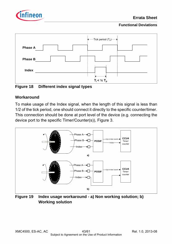
WorkaroundTo make usage of the Index signal, when the length of this signal is less than1/2 of the tick period, one should connect it directly to the specific counter/timer.This connection should be done at port level of the device (e.g. connecting thedevice port to the specific Timer/Counter(s)), Figure 3.
Figure 19 Index usage workaround - a) Non working solution; b) Working solution
Phase B
Phase A
Tick period (Tp)
Index
Ti < ½ Tp
POSIF
Phase A
Phase B
Index
CCU4Timer/counter
Up or dow count
Index
POSIF
Phase A
Phase B
Index
CCU4Timer/counter
Up or dow count
a)
b)
Errata SheetFunctional Deviations
XMC4500, ES-AC, AC 44/61 Rel. 1.0, 2013-08Subject to Agreement on the Use of Product Information
RTC_CM.001 RTC event might get lost
RTC interrupt may get cleared in the RTC module before propagated to theCPU interrupt controller.Single-shot RTC alarm may be missed. Periodic alarm events may be missedat the rate of once in 15 seconds.
ImplicationsRTC alarm interrupt alone cannot be reliably used for critical control functions. Note: Wake-up from hibernate mode is not affected and RTC timer value is
always correct.
WorkaroundWhile in active mode use alternate timer for periodic event trigger and/or readthe RTC timer value periodically.
SCU_CM.002 Missed wake-up event during entering external hibernatemode
Single-shot wake-up event and/or the first occurrence of a periodic wake-upevent from hibernate mode may be missed if it occurs within 200 microsecondsafter hibernate mode request issued in software.A wake-up event may be missed if it gets triggered during the process ofentering hibernate mode i.e. between software access to the hibernate controlregister and the moment hibernate mode is effectively entered.
ImplicationsWhile entering hibernate mode it is required that expected wake-up event willnot occur in the next 200 microseconds which not always may be guaranteed ifexternal wake-up source is considered.
WorkaroundUse of a backup wake-up event source generated internally with RTC may beapplied in order to compensate for the missing trigger after a defined time-out.

Errata SheetFunctional Deviations
XMC4500, ES-AC, AC 45/61 Rel. 1.0, 2013-08Subject to Agreement on the Use of Product Information
SCU_CM.003 The state of HDCR.HIB bit of HCU gets updated only oncein the register mirror after reset release
The state of HDCR.HIB bit of HCU gets updated only once in the register mirrorin SCU after system reset. Any write access to this register gets propagated tohibernate domain but it will be not propagated back to the register mirror whenaltered by the hardware inside of the hibernate domain.
ImplicationsThe state of HDCR.HIB cannot be effectively used for the purpose debuggingof hibernate mode control software.
WorkaroundFor debugging of the hibernate mode control software observe the electricalstates on the hibernate control pins in order to verify hibernate control circuitbehavior.
SCU_CM.006 Deep sleep entry with PLL power-down option generatesSOSCWDGT and SVCOLCKT trap
Entering the deep sleep mode with PLL power-down option (selected inDSLEEPCR register of SCU module) may result with system traps triggered byPLL watchdog (the SOSCWDGT trap) and/or loss-of-lock (the SVCOLCKTtrap).
ImplicationsOccurrence of one of the enabled traps will result in an immediate wake-up fromthe deep sleep state, i.e. the deep sleep is effectively not entered.
WorkaroundDisable SOSCWDGT and SVCOLCKT trap generation in TRAPDIS register ofSCU before entering deep sleep mode with PLL power-down option selected.
Errata SheetFunctional Deviations
XMC4500, ES-AC, AC 46/61 Rel. 1.0, 2013-08Subject to Agreement on the Use of Product Information
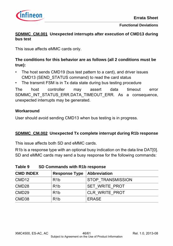
SDMMC_CM.001 Unexpected interrupts after execution of CMD13 duringbus test
This issue affects eMMC cards only.
The conditions for this behavior are as follows (all 2 conditions must be true):• The host sends CMD19 (bus test pattern to a card), and driver issues
CMD13 (SEND_STATUS command) to read the card status• The transmit FSM is in Tx data state during bus testing procedureThe host controller may assert data timeout errorSDMMC_INT_STATUS_ERR.DATA_TIMEOUT_ERR. As a consequence,unexpected interrupts may be generated.
WorkaroundUser should avoid sending CMD13 when bus testing is in progress.
SDMMC_CM.002 Unexpected Tx complete interrupt during R1b response
This issue affects both SD and eMMC cards.R1b is a response type with an optional busy indication on the data line DAT[0].SD and eMMC cards may send a busy response for the following commands:
Table 9 SD Commands with R1b responseCMD INDEX Response Type AbbreviationCMD12 R1b STOP_TRANSMISSIONCMD28 R1b SET_WRITE_PROTCMD29 R1b CLR_WRITE_PROTCMD38 R1b ERASE

Errata SheetFunctional Deviations
XMC4500, ES-AC, AC 47/61 Rel. 1.0, 2013-08Subject to Agreement on the Use of Product Information
When the card is in busy state for R1b, and driver sends the SEND_STATUScommand (CMD13) to read the card status. Due to this CMD13, unexpectedtransfer complete interrupt SDMMC_INT_STATUS_NORM.TX_COMPLETEmay be asserted by the host controller even before the busy signal getsreleased by the card.
WorkaroundUser should avoid sending CMD13 while the card is in busy state for R1b.
USB_CM.002 GAHBCFG.GlblIntrMsk not cleared with a software reset
When the application issues a software reset to the core through theGRSTCTL.CSftRst bit, the GAHBCFG.GlblIntrMsk bit is not reset to 0.Therefore, an interrupt will be generated in case any of the individual interruptmask bit (in GINTMSK) is unmasked after the software reset by the application.
WorkaroundThe workaround is to clear GAHBCFG.GlblIntrMsk to 0 immediately afterGRSTCTL.CSftRst is programmed for software reset.
Table 10 eMMC Commands with R1b responseCMD INDEX Response Type AbbreviationCMD5 R1b SLEEP_AWAKECMD6 R1b SWITCHCMD12 R1b STOP_TRANSMISSIONCMD28 R1b SET_WRITE_PROTCMD29 R1b CLR_WRITE_PROTCMD38 R1b ERASE

Errata SheetFunctional Deviations
XMC4500, ES-AC, AC 48/61 Rel. 1.0, 2013-08Subject to Agreement on the Use of Product Information
USIC_AI.005 Only 7 data bits are generated in IIC mode when TBUF isloaded in SDA hold time
When the delay time counter is used to delay the data line SDA (HDEL > 0), andthe empty transmit buffer TBUF was loaded between the end of theacknowledge bit and the expiration of programmed delay time HDEL, only 7 databits are transmitted.With setting HDEL=0 the delay time will be tHDEL = 4 x 1/fSYS + delay(approximately 60ns @ 80MHz).
Workaround• Do not use the delay time counter, i.e use only HDEL=0 (default),
or• write TBUF before the end of the last transmission (end of the acknowledge
bit) is reached.
USIC_AI.006 Dual SPI format not supported
Dual SPI format is not supported in SSC mode. Therefore, user should alwaysconfigure either the standard SPI or Quad SPI format in this mode.
WorkaroundNone.
USIC_AI.007 Protocol-related argument and error bits in register RBUF-SR contain incorrect values following a received data word
The protocol-related argument and error bits (PAR and PERR respectively) inregister RBUFSR contain incorrect values following a received data word. Thisleads to the following errors:

Errata SheetFunctional Deviations
XMC4500, ES-AC, AC 49/61 Rel. 1.0, 2013-08Subject to Agreement on the Use of Product Information
WorkaroundThe workarounds are summarized below:
Table 11Protocol Error due to incorrect PAR and PERR valuesASC • Received parity bit (RBUFSR.PAR) and result of the parity
check (RBUFSR.PERR) are incorrect.• When a data word is received, an alternate receive event
(PSR.AIF) may be indicated instead of a receive event (PSR.RIF) even though parity mode is disabled.
SSC • Received parity bit (RBUFSR.PAR) and result of parity check (PSR.PAERR) are incorrect.
• The first data word of a frame may be indicated by a receive event (PSR.RIF) instead of an alternate receive event (PSR.AIF). Similarly, a data word that is not the first word of a frame may be indicated by PSR.AIF instead of PSR.RIF.
IIC • Received acknowledge bit in RBUFSR.PAR is incorrect.• The first data word of a frame may be indicated by a receive
event (PSR.RIF) instead of an alternate receive event (PSR.AIF). Similarly, a data word that is not the first word of a frame may be indicated by PSR.AIF instead of PSR.RIF.
IIS • Sampling of condition WA = 1 may be indicated by a receive event (PSR.RIF) instead of an alternate receive event (PSR.AIF). Similarly, sampling of condition WA = 0 may be indicated by PSR.AIF instead of PSR.RIF.

Errata SheetFunctional Deviations
XMC4500, ES-AC, AC 50/61 Rel. 1.0, 2013-08Subject to Agreement on the Use of Product Information
USIC_AI.008 Bit SCLKOSEL in register BRG not implemented
In SSC slave mode, setting the bit SCLKOSEL in register BRG to one selectsthe transmit shift clock as the signal SCLKOUT input source. This is requiredfor a complete closed loop delay compensation.However, in the current device version, the bit SCLKOSEL is not implementedand setting the bit to one has no effect. The bit remains always zero. Therefore,the complete closed loop delay compensation feature cannot be supported.
Table 12Protocol WorkaroundASC • Parity mode cannot be used.
• To check if a data word is received, both PSR.RIF and PSR.AIF flags need to be monitored. If interrupts are used, interrupt service handlers need to be set up for both interrupt sources.
SSC • Parity mode cannot be used.• To check if a data word is received, both PSR.RIF and PSR.AIF
flags need to be monitored. If interrupts are used, interrupt service handlers need to be set up for both interrupt sources.
• To check if a data word is the first data word of a frame, the bit RBUFSR.SOF can be used.
IIC • To check for the acknowledge bit, bit 8 of the receive buffer RBUF can be used.
• To check if a data word is received, both PSR.RIF and PSR.AIF flags need to be monitored. If interrupts are used, interrupt service handlers need to be set up for both interrupt sources.
• To check if a data word is the first data word of a frame, bit 9 of RBUF can be used.
IIS • To check if a data word is received, both PSR.RIF and PSR.AIF flags need to be monitored. If interrupts are used, interrupt service handlers need to be set up for both interrupt sources.
• To check the sampled value of WA, the bit PSR.WA can be used.

Errata SheetFunctional Deviations
XMC4500, ES-AC, AC 51/61 Rel. 1.0, 2013-08Subject to Agreement on the Use of Product Information
WorkaroundNone.
USIC_AI.009 Baud rate generator interrupt cannot be used
The baud rate generator interrupt cannot be used. The bit CCR.BRGIEN mustalways be written with zero to disable baud rate generator interrupt generation.
WorkaroundNone.
USIC_AI.010 Minimum and maximum supported word and frame length inmulti-IO SSC modes
The minimum and maximum supported word and frame length in multi-IO SSCmodes are shown in the table below:
WorkaroundIf a frame length greater than 64 data bits is required, the generation of themaster slave select signal by SSC should be disabled by PCR.MSLSEN. To generate the master slave select signal:• Configure the same pin (containing the SELOx function) to general purpose
output function instead by writing 10000B to the pin’s input/output control register (Pn_IOCRx.PCy); and
• Use software to control the output level to emulate the master slave select signal
Table 13Multi-IO SSC Modes Word Length (bits) Frame Length (bits)
Minimum Maximum Minimum MaximumDual-SSC 4 16 4 64Quad-SSC 8 16 8 64

Errata SheetFunctional Deviations
XMC4500, ES-AC, AC 52/61 Rel. 1.0, 2013-08Subject to Agreement on the Use of Product Information
This way, multiple frames of 64 data bits can be made to appear as a singlemuch larger frame.
USIC_AI.011 Write to TBUF01 has no effect
Writing data to Transmit Buffer Input Location 01 (register TBUF01 at offsetaddress 084H) does not load the data to the transmit buffer (TBUF).
WorkaroundUse registers TBUF00 or TBUFx (x = 02 to 31) to load data to the transmitbuffer.If the Transmit Control Information (TCI) value of 00001B needs to be generatedtogether with the load to TBUF, use a FIFO setup and Transmit FIFO BufferInput location 01 (register IN01 at offset address 184H) instead.
USIC_AI.013 SCTR register bit fields DSM and HPCDIR are not shadowedwith start of data word transfer
The bit fields DSM and HPCDIR in register SCTR are not shadowed with thestart of a data word transfer.
WorkaroundIf the transfer parameters controlled by these bit fields need to be changed forthe next data word, they should be updated only after the current data wordtransfer is completed, as indicated by the transmit shift interrupt PSR.TSIF.
USIC_AI.014 No serial transfer possible while running capture mode tim-er
When the capture mode timer of the baud rate generator is enabled(BRG.TMEN = 1) to perform timing measurements, no serial transmission orreception can take place.

Errata SheetFunctional Deviations
XMC4500, ES-AC, AC 53/61 Rel. 1.0, 2013-08Subject to Agreement on the Use of Product Information
WorkaroundNone.
USIC_AI.015 Wrong generation of FIFO standard transmit/receive bufferevents when TBCTR.STBTEN/RBCTR.SRBTEN = 1
Transmit FIFO buffer modes selected by TBCTR.STBTEN = 1 generates astandard transmit buffer event whenever TBUF is loaded with the FIFO data orthere is a write to INxx register, except when TRBSR.TBFLVL = TBCTR.LIMIT.This is independent of TBCTR.LOF setting.Similarly, receive FIFO buffer modes selected by RBCTR.SRBTEN = 1generates a standard receive buffer event whenever data is read out from FIFOor received into the FIFO, except when TRBSR.RBFLVL = RBCTR.LIMIT. Thisis independent of RBCTR.LOF setting.Both cases result in the wrong generation of the standard transmit and receivebuffer events and interrupts, if interrupts are enabled.
WorkaroundUse only the modes with TBCTR.STBTEN and RBCTR.SRBTEN = 0.
USIC_AI.016 Transmit parameters are updated during FIFO buffer bypass
Transmit Control Information (TCI) can be transferred from the bypass structureto the USIC channel when a bypass data is loaded into TBUF. Depending onthe setting of TCSR register bit fields, different transmit parameters are updatedby TCI:• When SELMD = 1, PCR.CTR[20:16] is updated by BYPCR.SELO
(applicable only in SSC mode)• When WLEMD = 1, SCTR.WLE and TCSR.EOF are updated by
BYPCR.BWLE• When FLEMD = 1, SCTR.FLE[4:0] is updated by BYPCR.BWLE• When HPCMD = 1, SCTR.HPCDIR and SCTR.DSM are updated by BHPC• When all of the xxMD bits are 0, no transmit parameters will be updated
Errata SheetFunctional Deviations
XMC4500, ES-AC, AC 54/61 Rel. 1.0, 2013-08Subject to Agreement on the Use of Product Information
However in the current device, independent of the xxMD bits setting, thefollowing are always updated by the TCI generated by the bypass structure,when TBUF is loaded with a bypass data:• WLE, HPCDIR and DSM bits in SCTR register• EOF and SOF bits in TCSR register• PCR.CTR[20:16] (applicable only in SSC mode)
WorkaroundThe application must take into consideration the above behaviour when usingFIFO buffer bypass.
USIC_AI.018 Clearing PSR.MSLS bit immediately deasserts the SELOxoutput signal
In SSC master mode, the transmission of a data frame can be stopped explicitlyby clearing bit PSR.MSLS, which is achieved by writing a 1 to the related bitposition in register PSCR.This write action immediately clears bit PSR.MSLS and will deassert the slaveselect output signal SELOx after finishing a currently running word transfer andrespecting the slave select trailing delay (Ttd) and next-frame delay (Tnf).However in the current implementation, the running word transfer will also beimmediately stopped and the SELOx deasserted following the slave selectdelays.If the write to register PSCR occurs during the duration of the slave selectleading delay (Tld) before the start of a new word transmission, no data will betransmitted and the SELOx gets deasserted following Ttd and Tnf.
WorkaroundThere are two possible workarounds:• Use alternative end-of-frame control mechanisms, for example, end-of-
frame indication with TSCR.EOF bit.• Check that any running word transfer is completed (PSR.TSIF flag = 1)
before clearing bit PSR.MSLS.

Errata SheetDeviations from Electrical- and Timing Specification
XMC4500, ES-AC, AC 55/61 Rel. 1.0, 2013-08Subject to Agreement on the Use of Product Information
3 Deviations from Electrical- and Timing Specification
The errata in this section describe deviations from the documented electrical-and timing specifications.
DAC_CM.P001 INL parameter limits violated by some devices
At some devices the DAC module violates the Integral Nonlinearity (INL)parameter limits of ±4 LSB, especially for very cold temperatures. Thesedevices can show INL values up to ±5.5 LSB, measured with best straight linemethod.Note: Integral Nonlinearity (INL) is defined as the max. deviation of the output
characteristic against a straight line. Selecting the straight line which gives best INL number, is called best straight line method.
Errata SheetApplication Hints
XMC4500, ES-AC, AC 56/61 Rel. 1.0, 2013-08Subject to Agreement on the Use of Product Information
4 Application HintsThe errata in this section describe application hints which must be regarded toensure correct operation under specific application conditions.
ADC_AI.H003 Injected conversion may be performed with sample time ofaborted conversion
For specific timing conditions and configuration parameters, a higher prioritizedconversion ci (including a synchronized request from another ADC kernel) incancel-inject-repeat mode may erroneously be performed with the sample timeparameters of the lower prioritized cancelled conversion cc. This can lead towrong sample results (depending on the source impedance), and may also shiftthe starting point of following conversions.The conditions for this behavior are as follows (all 3 conditions must be met):1. Sample Time setting: injected conversion ci and cancelled conversion cc
use different sample time settings, i.e. bit fields STC* in the corresponding Input Class Registers for cc and for ci (GxICLASS0/1, GLOBICLASS0/1) are programmed to different values.
2. Timing condition: conversion ci starts during the first fADCI clock cycle of the sample phase of cc.
3. Configuration parameters: the ratio between the analog clock fADCI and the arbiter speed is as follows: NA > ND*(NAR+3), witha) NA = ratio fADC/fADCI (NA = 2 .. 32, as defined in bit field DIVA),b) ND = ratio fADC/fADCD = number of fADC clock cycles per arbitration slot
(ND = 1 .. 4, as defined in bit field DIVD),c) NAR = number of arbitration slots per arbitration round (NAR = 4, 8, 16, or
20, as defined in bit field GxARBCFG.ARBRND).Bit fields DIVA and DIVD mentioned above are located in register GLOBCFG.As can be seen from the formula above, a problem typically only occurs whenthe arbiter is running at maximum speed, and a divider NA > 7 is selected toobtain fADCI.
Errata SheetApplication Hints
XMC4500, ES-AC, AC 57/61 Rel. 1.0, 2013-08Subject to Agreement on the Use of Product Information
Recommendation 1Select the same sample time for injected conversions ci and potentiallycancelled conversions cc, i.e. program all bit fields STC* in the correspondingInput Class Registers for cc and for ci (GxICLASS0/1, GLOBICLASS0/1) tothe same value.
Recommendation 2Select the parameters in register GLOBCFG and GxARBCFG according to thefollowing relation: NA ≤ ND*(NAR+3).
ADC_AI.H004 Completion of Startup Calibration
Before using the VADC the startup calibration must be completed. The calibration is started by setting GLOBCFG.SUCAL. The active phase of thecalibration is indicated by GxARBCFG.CAL = 1. Completion of the calibration isindicated by GxARBCFG.CAL = 0.When checking for bit CAL = 1 immediately after setting bit SUCAL, bit CALmight not yet be set by hardware. As a consequence the active calibrationphase may not be detected by software.The software may use the followingsequence for startup calibration:1. GLOBCFG.SUCAL = 1 2. Wait for GxARBCFG.CAL = 13. Check for GxARBCFG.CAL = 0 before starting a conversionMake sure that steps 1 and 2 of this sequence are not interrupted to avoid adeadlock situation with waiting for GxARBCFG.CAL = 1.
MultiCAN_AI.H005 TxD Pulse upon short disable request
If a CAN disable request is set and then canceled in a very short time (one bittime or less) then a dominant transmit pulse may be generated by MultiCANmodule, even if the CAN bus is in the idle state.Example for setup of the CAN disable request:

Errata SheetApplication Hints
XMC4500, ES-AC, AC 58/61 Rel. 1.0, 2013-08Subject to Agreement on the Use of Product Information
WorkaroundSet all INIT bits to 1 before requesting module disable.
MultiCAN_AI.H006 Time stamp influenced by resynchronization
The time stamp measurement feature is not based on an absolute timemeasurement, but on actual CAN bit times which are subject to the CANresynchronization during CAN bus operation.The time stamp value merelyindicates the number of elapsed actual bit times. Those actual bit times can beshorter or longer than nominal bit time length due to the CAN resynchronizationevents.
WorkaroundNone.
MultiCAN_AI.H007 Alert Interrupt Behavior in case of Bus-Off
The MultiCAN module shows the following behavior in case of a bus-off status:
Figure 20 Alert Interrupt Behavior in case of Bus-Off
When the threshold for error warning (EWRN) is reached (default value of ErrorWarning Level EWRN = 0x60), then the EWRN interrupt is issued. The bus-off(BOFF) status is reached if TEC > 255 according to CAN specification,changing the MultiCAN module with REC and TEC to the same value 0x1,setting the INIT bit to 1B, and issuing the BOFF interrupt. The bus-off recoveryphase starts automatically. Every time an idle time is seen, REC is incremented.If REC = 0x60, a combined status EWRN+BOFF is reached. The correspondinginterrupt can also be seen as a pre-warning interrupt, that the bus-off recovery
TEC=0x60 or REC=0x60
EWRN
REC=0x1, TEC=0x1
BOFFINIT
REC=0x60, TEC=0x1
EWRN+BOFFINIT
REC=0x0, TEC=0x0
ALERTINIT
Errata SheetApplication Hints
XMC4500, ES-AC, AC 59/61 Rel. 1.0, 2013-08Subject to Agreement on the Use of Product Information
phase will be finished soon. When the bus-off recovery phase has finished (128times idle time have been seen on the bus), EWRN and BOFF are cleared, theALERT interrupt bit is set and the INIT bit is still set.
MultiCAN_AI.H008 Effect of CANDIS on SUSACK
When a CAN node is disabled by setting bit NCR.CANDIS = 1B, the node waitsfor the bus idle state and then sets bit NSR.SUSACK = 1B. However, SUSACK has no effect on applications, as its original intention is tohave an indication that the suspend mode of the node is reached duringdebugging.
MultiCAN_TC.H003 Message may be discarded before transmission inSTT mode
If MOFCRn.STT=1 (Single Transmit Trial enabled), bit TXRQ is cleared(TXRQ=0) as soon as the message object has been selected for transmissionand, in case of error, no retransmission takes places.Therefore, if the error occurs between the selection for transmission and thereal start of frame transmission, the message is actually never sent.
WorkaroundIn case the transmission shall be guaranteed, it is not suitable to use the STTmode. In this case, MOFCRn.STT shall be 0.
MultiCAN_TC.H004 Double remote request
Assume the following scenario: A first remote frame (dedicated to a messageobject) has been received. It performs a transmit setup (TXRQ is set) withclearing NEWDAT. MultiCAN starts to send the receiver message object (dataframe), but loses arbitration against a second remote request received by thesame message object as the first one (NEWDAT will be set).

Errata SheetApplication Hints
XMC4500, ES-AC, AC 60/61 Rel. 1.0, 2013-08Subject to Agreement on the Use of Product Information
When the appropriate message object (data frame) triggered by the first remoteframe wins the arbitration, it will be sent out and NEWDAT is not reset. This leadsto an additional data frame, that will be sent by this message object (clearingNEWDAT).There will, however, not be more data frames than there are correspondingremote requests.
Figure 21 Loss of Arbitration
RESET_CM.H001 Power-On Reset Release
The on-chip EVR implements a power validation circuitry which supervisesVDDP and VDDC. This circuit releases or asserts the system reset to ensuresafe operation. This reset is visible on bidirectional PORST pin.
ImplicationsPotential effects if the PORST release requirement is not met (please refer tothe Data Sheet for details) is presence of spikes or toggling on the PORST pinwhich may have an effect on the rest of the system if the reset signal is sharedwith other electronic components on the PCB. A repeated PORST may alsoresult in loss of information about hibernation status after an interrupted wake-up has been performed. Potential presence of the spikes on PORST, however,will not lead to a fatal system startup failure or deadlock.
re m o tere q u e s t
d a tao b je c t
C A N B u s
M u ltiC A N s e tu p
c le a rN E W D A T
d a tao b je c t
lo ss o fa rb itra tio n
se tu p
s e tN E W D A T
s e tu p d a tao b je c t
c le a rN E W D A T
re m o tere q u e s t
b y H W b y H W b y H W
d a ta d a ta
c le a r

Errata SheetApplication Hints
XMC4500, ES-AC, AC 61/61 Rel. 1.0, 2013-08Subject to Agreement on the Use of Product Information
RecommendationIt is required to ensure fast PORST release, as specified in Data Sheet. Therecommended approach is to apply a pull-up resistor on the PORST pin.Typically a 10 - 90 k? resistor is sufficient in application cases where the deviceis in control of the reset generation performed by its internal power validationcircuit and no additional load is applied to the PORST pin. The required pull-upresistor value may vary depending on the electrical parameters of the system,like parasitic wire resistance and capacitance of the PCB, driving strength ofother electronic components connected to the PORST pin and other sideconditions. The pull-up resistance may need to be adapted accordingly.