xps and raman studies on (002) oriented nanocrystalline ...€¦ · xps and raman studies 157...
TRANSCRIPT

Adv. Studies Theor. Phys., Vol. 5, 2011, no. 4, 155 - 170
XPS and Raman Studies on (002) Oriented
Nanocrystalline ZnO Films Showing Temperature
Dependent Optical Red Shift
K. Saravanakumar
PG and Research Department of Physics Kongunadu Arts and Science College
Coimbatore -29, India
C. Gopinathan and K. Mahalakshmi
PG and Research Department of Physics The Madura College, Madurai – 625 011, India
V. Ganesan, V. Sathe
UGC-DAE Consortium for Scientific Research Khandwa Road, Indore 452 017, India.
C. Sanjeeviraja∗
Department of Physics, Alagappa University
Karaikudi – 630 003, India * Corresponding author [email protected]

156 K. Saravanakumar et al
Abstract Nanocrystalline zinc oxide (ZnO) thin films have been prepared on glass
substrates at different temperatures through planar RF-magnetron sputtering. Structural properties with respect to substrate temperature have been studied with x-ray diffraction (XRD) patterns. The stoichiometry in the films is studied with X-ray photoemission spectroscopy (XPS). The shifts in the absorption edge of the films in the optical spectrum with the variation of substrate temperature are examined. Raman spectrum showed an increase in the average scattering intensity of the phonon peak at 580 cm-1 with respect to the reduction of particle size. The variation of conductivity of prepared ZnO films with respect to substrate temperature is studied well. Keywords: ZnO, XPS, Raman 1. Introduction
ZnO is an II–VI type semiconductor of wurtzite structure with ions connected with four counter ions in the tetrahedral bond of sp3 hybridization [1]. The material is widely studied because of its low toxicity and unique properties such as wide band gap of 3.3 eV and large excitonic binding energy of 60 meV at room temperature [2]. These interesting properties have made ZnO useful in developing many devices like transparent electrodes, solar cell windows [3], piezoelectric actuators [4], gas sensors [5], surface acoustic wave devices [6] and heat mirrors [7]. The report says that the use of ZnO blue lasers in a CD writer could increase the amount of data storage by four times [8]. It is also reported that ordered nanocrystalline ZnO films exhibit important piezo and optoelectric properties [9,10]. From the fundamental of nanoscience, it is believed that the reduction of nanograin size of a material to further, novel electrical, mechanical and optical properties to be introduced in the material due to surface and quantum confinement effects which lead to the fabrication novel devices.
Keeping this in mind the nanocrystalline ZnO films are prepared by RF-Magnetron Sputtering Unit on corning glass substrates by varying the substrate temperature. The effects of substrate temperature on the structural properties of the films are studied.
With the aim to improve the nature and performance of ZnO films, using many deposition techniques, chemical and physical routes, have been developed such as chemical vapor deposition (CVD) [11], spray pyrolysis [12], ion-beam assisted deposition [13] and Magnetron sputtering [14]. In this respect, RF Magnetron
XPS and Raman studies 157 sputtering is preferred due its reproducibility and for getting highly oriented films. This physical route is used to produce films with the desired optoelectronic and nanostructure properties by precisely controlling the parameters like Ar-O2 flux deposition pressure, target-substrate distance, RF power and substrate temperature.
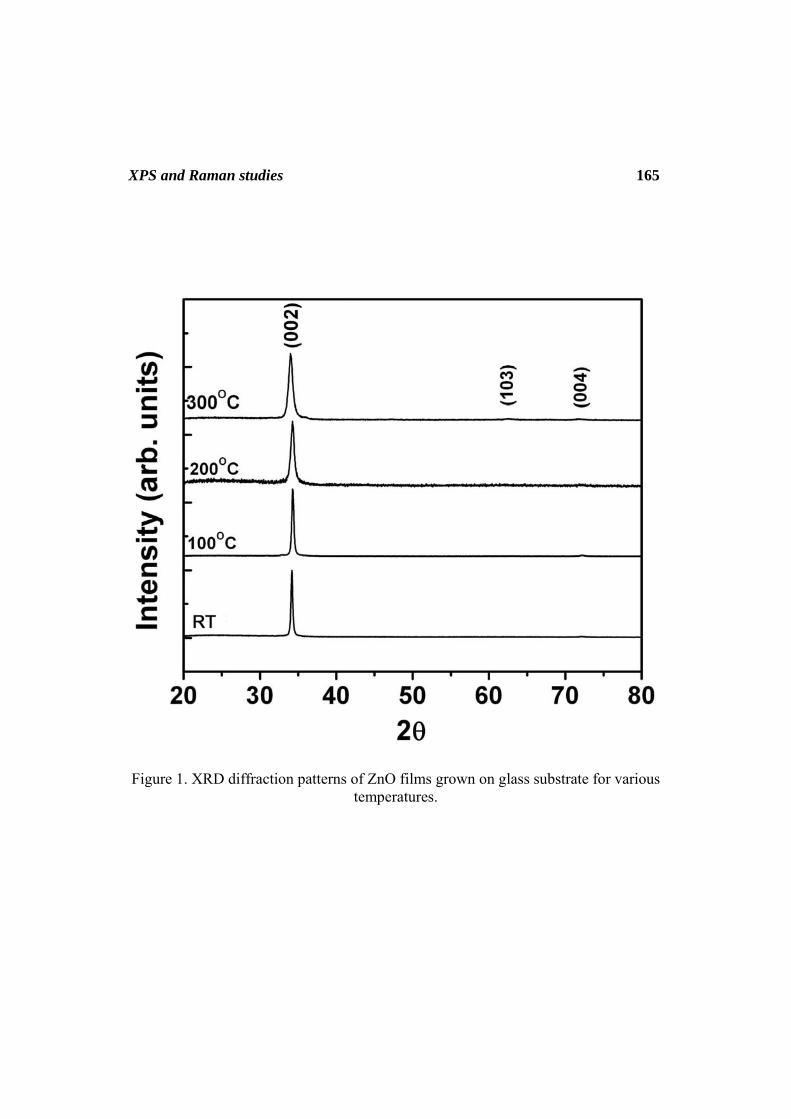
Keeping the economic point in view of commercial applications of ZnO and for to study the properties of the nanocrystalline ZnO, we have made an attempt to produce ZnO nanocrystalline films in the absence of oxygen environment on glass substrates using RF magnetron sputtering. In this communication, we report the studies on the effect of substrate temperature on the growth of highly textured nanocrystalline ZnO thin films. 2. Experimental Details Thin films were prepared by planar RF-magnetron sputtering from ZnO target (99.99%, Super conductors, USA). The target had a diameter of 50 mm and thickness of 5 mm and the substrate was set at a distance of 6 cm above the target. Corning 7059 glass plates were used as substrates. Before deposition, the chamber was evacuated to an ultimate background pressure of 10-6 mbar for 1 h and pre-sputtering process employed for 10 min to clean the target surface. High purity Ar (99.999%) was used as sputtering gas. The Ar flow was introduced directly into dark space shields of the sputtering sources. The sputtering gas pressure was controlled by adjusting a needle valve and the deposition pressure in the chamber was maintained at 10-4 mbar. Substrate temperature was varied from room temperature (RT) to 300ºC, and the RF power was maintained at 200W. The deposition usually lasted for 30 min. The structure and phase purity characterization of the films was carried out with a Rigaku X-ray diffractometer using CuKα radiation. XPS spectra was recorded by VG ESCA LAB MK II spectrometer using Al Kα (1486.6 eV) radiation from an X-ray source operated at 12 kV, 10mA. The optical transmittance of the films was studied using a UV-Vis-NIR spectrophotometer (CARY-5 Model) with a cleaned corning glass in the reference beam. Raman measurements of these samples were performed using Horiba Jobin Yvon LABRAM-HR spectrometer with an excitation wavelength of 400 nm in the back scattering geometry at room temperature. Resistivity measurements were done with the help of standard four-probe technique. 3. XRD analysis Figure 1 shows the XRD patterns of the ZnO thin films deposited at RT, 100, 200 and 300 oC substrate temperatures. The XRD profiles of films reveal an intense

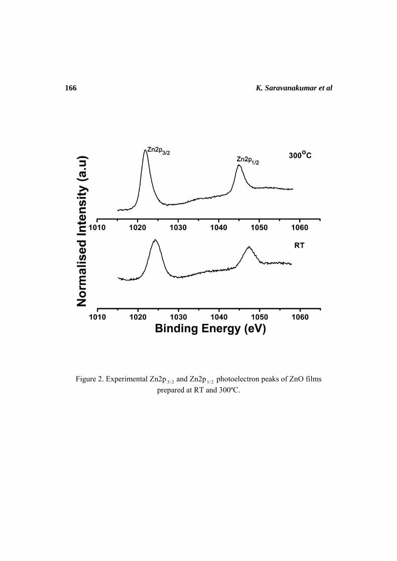
158 K. Saravanakumar et al diffraction peak oriented along (002) plane and a small diffraction peak oriented along (004) plane confirms the wurtzite phases of ZnO. This indicates that the growth of ZnO films is highly oriented along c-axis. At a substrate temperature of 300ºC, an another peak appears with (103) orientation with less intensity. The appearance of this peak is due to the defects produced at higher substrate temperature because of the relocating of atoms during the deposition [15]. The mean crystallite sizes (DXRD) were calculated using the Scherrer formula, DXRD=0.94λ/(β cos θβ), where λ, θβ, and β are the x-ray wavelength, Bragg diffraction angle, and the line width at half maximum of the diffraction peak, respectively and were given in table 1. These values show that the crystallite size is decreasing with increasing substrate temperature. Film stress (σfilm) was obtained from XRD using biaxial strain model and the formula, σfilm = -233 ε was used for calculating the stress parallel to the film surface, where ε = (Cfilm – Cbulk)/Cbulk, the strain in the direction of the c-axis, i.e., perpendicular to the substrate surface [16], Cfilm is the lattice parameter values of the films and Cbulk value was taken as 5.205 Å [17]. The calculated stress values are given in table 1. From the stress values it is inferred that the tensile stress is acting on the film and it is found decreasing when the substrate temperature increased to 200ºC and then increased drastically with further increase in temperature. The decrease in stress is due to the enhancement in the adatom mobility by increasing the substrate temperature. The increase in stress may be due to the mechanical strain that was introduced in the film when the film is cooled to room temperature from higher substrate temperature. The further increase in stress was due to the defects produced in the film at higher substrate temperature. Dislocation density (δ) was calculated using the formula, δ=1/(DXRD)2 and the values are given in table 1. It is observed that the δ value increases with increasing substrate temperature. 4. Elemental Analysis A comparative study of the stoichiometry of ZnO films deposited at RT and 300ºC was carried out here. XPS spectra of ZnO films were analysed to investigate the chemical states of Zn and O and their percentage in ZnO film. Figure 2 is the experimental Zn2p 3/ 2 and Zn2p 1/ 2 photoelectron peaks of ZnO films prepared at RT and 300ºC after 3 min Ar+ (800V) sputter cleaning. From figures 2 and 3, the peak positions of Zn2p 3/ 2 , Zn2p 1/ 2 and O1s are in good agreement with the reported values. It can be seen from the figure 2 that the Zn percentage is more in the film deposited at 300ºC. Figure 3 is a experimental O1s photoelectron peak of ZnO films prepared at RT and 300ºC. The film deposited at 300ºC shows the intensity asymmetry towards high energy and this was not observed in the film deposited at RT. This explains the oxygen get decreased at higher temperature. This is due to the

XPS and Raman studies 159 insufficient oxygen atmosphere during the film growth. The shifting of Zn2p 3/ 2 ,
Zn2p1/ 2 and O1s peak was observed from the XPS spectra. The shift in these core level peaks explains the H2O, CO2, etc., from exposure to air is not completely removed in the sputter cleaning [18]. The Zn/O ratio was calculated by selecting the Zn2p 3/ 2 and O1s line peaks. It is observed that the film deposited at RT shows the value of 1.57 and the film deposited at 300ºC shows 3.89. From these values, it is clearly evidenced that the oxygen percentage is decreased in the film deposited at 300ºC. It is also reported that the oxygen gets re-evaporated from the surface at higher substrate temperatures [19].
Because of the oxygen deficiency during the growth, excess zinc is produced which occupies the interstitial positions in the crystal lattice formed as native defects. The most mobile defects in ZnO films are zinc interstitials followed by oxygen interstitials, zinc vacancies and oxygen vacancies. Density functional theory calculations show the zinc intersititials to migrate in the vicinity of the grain boundaries and oxygen vacancies to be rather immobile [20]. From this consideration, the zinc atoms migrated near the grain boundaries act as a barrier for the further growth of grain boundaries which in turn decreases the grain size. By increasing the substrate temperature there is a possibility of more zinc atoms produced due to the oxygen deficiency, this will decrease the grain further. 5. Optical Studies Figure 4 is a transmission spectra of RF sputtered ZnO films. All films showed >85% transmission in the visible region. Interference pattern indicates that the film would have excess zinc sites at the grain boundaries which reflect the light intensity. The absence of interference pattern in the film deposited at RT was due to the formation of grainy surface leading to large scattering loss [21].
Based on the basic absorption relation 0ln lnT T tα= − , where T is the transmitted light intensity, T0 is the illuminated light intensity, α is the absorption coefficient and t is the thickness of the film, one could write lnTα ∝ − [22], it explains the variations of T is mainly associated with α. Hence, we have plotted graphs between hν and ( ) 2
lnT hν−⎡ ⎤⎣ ⎦ for finding the optical band gap (Eg) of the prepared films. The Eg values were calculated using Tauc plot [23] as shown in the inset of figure 4, by extrapolating the linear line cut at the x-axis and the corresponding values are given in table 1. It is observed that the band gap of the film red-shifted from 3.248 eV to 3.16 eV by increasing the temperature from RT to 300°C. In our defect doped ZnO film, the dopant carriers could be the electrons and
160 K. Saravanakumar et al occupies the states in the bottom of the conduction band which may lower the conduction band edge downwards leading to a reducing the separation between the conduction and band the valence band. This may due to the semiconductor-metal transition [24] associated with some reduction in resistivity of the ZnO films deposited at higher substrate temperatures. 6. Raman Studies Wurtzite type ZnO belongs to the C6v (P63mc) space symmetry. Each unit cell is having 4 atoms and occupying 2b sites of symmetry C3v. At the point near the Brillouin zone the following optical phonon modes are allowed, Пopt = A1+2B1+E1+2E2. Among these, doubly degenerate B1 modes are silent, A1 and E1 branches are both Raman and infrared active, and other doubly degenerate E2 modes are Raman active. Figure 5 shows the Raman spectra of ZnO films grown at RT and 300ºC. Appearance of the peak near 275 cm-1 was attributed to the B1 silent inactive mode. Raman active phonon mode E2 (TO) was observed near to 438 cm-1. Another mode observed around 580 cm-1 attributed to E1 (LO) branch. The optical phonon modes confirm that the synthesized nanocystalline films have the wurtzite hexagonal phase. The peak position at 580 cm-1 itself is enhanced compared to other peak positions while increasing the substrate temperature. Many researchers have found that the Raman mode at this peak position corresponds to silent modes [25], Nitrogen-related vibrational modes [26] and defect associated with zinc interstitials, oxygen vacancies or their combination [27]. In our case, the appeared peak is due to the native defects produced in the film, when the particle size decreases, it increases the surface to volume ratio so that the defect related states also increases. Due to these changes, the scattering intensity of the respective phonon peak gets increased. Approximately 1.5 cm-1 shift was observed in the peak position of the ZnO film deposited at 300ºC to the room temperature deposited film. This shift indicates that the compressive stress was acting normal to the film while increasing the substrate temperature. Further, the intensity also increased considerably. The scattering area was calculated by Gaussian fits and it was found that the film deposited at 300ºC scattered 1.5 times greater than the film deposited at RT. This phenomena indicates the characteristic behaviours associated with reduction in particle size that the average scattering intensity from small particles is greater than from the larger particles.

XPS and Raman studies 161 7. Electrical Studies Linear four probe method was adopted for measuring the dc conductivity of the films. Figure 6 shows the variation of conductivity of the films with different temperatures. The conductivity increases with increase in the substrate temperature which indicates that native defects are increased more. It is also inferred from the figure that the prepared films show the semiconducting behaviour. Arrhenius plot of ln ρ, where ρ is the resistivity versus inverse of temperature is shown in the inset of Figure 6. The plot is linear over ten orders of magnitude and using the relation ρ = ρo exp(-ΔE/kT), the activation energy ΔE was estimated for all the films. The values are less than the half of the optical band gap values, indicating that the film conduction is extrinsic in nature. During the deposition the mobility of the carrier is increased at the grain boundaries because of the presence of zinc atoms at the grain boundaries which decreases the activation energy. It is reported that the activation energy was more associated with activated mobility rather than the charge carriers [28]. Conclusions In summary, highly textured ZnO films have been grown successfully on amorphous glass substrates at various substrate temperatures. The XRD results showed the particle size reduction with increasing substrate temperature. The bandgap and activation energy values are considerably decreased with the nanograin size. This is mainly because of the excess zinc atoms near the grain boundaries produced in the structure due to the oxygen deficiency and this was clearly evidenced from XPS spectra. Acknowledgements
The authors gratefully acknowledged UGC-DAE Consortium for scientific
research, Indore for the financial support. Also, the authors wish to thank the Director and Centre Director, UGC-DAE CSR, Indore for providing the facilities to perform this work. Authors thank Miss. Swathi pandya and Miss. DeeptiJain for their help in Conductivity measuerments.

162 K. Saravanakumar et al References [1] M. Tsukada, H. Adachi and C. Satoko, Prog. in Surf. Sci. 14 (1983)113. [2] Yoshitaka Nakano, Takeshi Morikawa, Takeshi Ohwaki and Yasunori Taga, Appl. Phys. Lett. 88 (2006) 172103. [3] N. Golego, S.A. Studenikin and M. Cocivera, J. Electrochem. Soc. 147 (2000) 1592. [4] S.B. Krupanidhi and M. Sayer, J. Appl. Phys. 56 (1984) 3308. [5] Y. Lin, Z. Zhang, Z. Tang, F. Yuan and J. Li, Adv. Mater. Opt. Electron. 9 (1999) 205. [6] J.F. Cordaro, Y. Shim and J.E. May, J. Appl. Phys. 60 (1996) 4186. [7] C.M. Lampert, Sol. Energy Mater. 6 (1981) 1. [8] R.F. Service, Science 276 (1997) 895. [9] Van De Pol, F C M, Ceram. Bull. 69 (1990) 1959. [10] M. Koch, P.Y. Timbrell and R.N. Lamb, Semiconductor Sci. Technol. 10 (1995)1523 [11] J. Hu, R.G. Gordon, J. Appl. Phys. 71 (1992) 880. [12] F. Paraguay, W. Estada, D.R. Acosta, E. Andarade and M. Miki Yoshida, Thin Solid Films 350 (1999) 192. [13] DH. Zhang and DE. Brodie, Thin Solid Films 238 (1994) 95. [14] BM. Han, S. Chang and S.Y. Kim, Thin Solid Films 338 (1999) 265. [15] A. Umar, B. Karunagaran, E-K. Suh and Y.B. Hahu, Nanotechnology 17 (2006) 4072 [16] R. Cebulla, R. Wendt and K. Ellmer, J. Appl. Phys. 83 (1998)1091.

XPS and Raman studies 163 [17] V.A. Karpina et al., Cryst. Res. Technol. 39 (2004) 980. [18] Ning Xu, Yinglizng Xu, Li Li, Yiqun Shen, Tinwel Zhang, Jiada Wu, Jian Sun and Zhifeng Ying, J. Vac. Sci. Technol. A 24 (2006) 517. [19] S.M. Jejurikar, A.G. Banpurkar, A.V. Limaye, S.K. Date, S.I. Patil, K.P. Adhi, P. Misra, L.M. Kukreja and Ravi Bathe, J. Appl. Phys. 99 (2006) 014907. [20] Paul Erhart and Karsten Albe, Appl. Phys. Lett. 88 (2006) 201918. [21] P.M. Ratheesh Kumar, C. Sudha Kartha, K.P. Vijayakumar, T. Abe, Y. Kashiwaba, F. Singh and D.K. Avasthi, Semicond. Sci. Technol. 20 (2005)120. [22] F.K. Shan, B.I. Kim, G.X. Liu, J.Y. Sohn, W.J. Lee, B.C. Shin and Y.S. Yu, J. Appl. Phys. 95 (2004) 4772. [23] J. Tauc, Amorphous and Liquid Semiconductors, plenum, New York, Ch. 4. [24] P. Alain, B. Roth, B. James. Webb and F. Digby. Williams Physical Review B 25 (1982)7836. [25] F.J. Manjon, B. Mari, J. Serrano and A.H. Romero, J. Appl. Phys. 97 (2005) 053516. [26] A. Kaschner, U. Haboeck, M. Strassburg, G. Kaczmarczyk, A. Hoffmann, C. Thomsen, A. Zeuner, H.R. Alves, D.M. Hofmann and B.K. Meyer, Appl. Phys. Lett. 80 (2002) 1909. [27] Z.Q. Chen, A. Kawasuso,Y. Xu, H. Naramoto, X.L. Yuan, T. Sekiguchi, R. Suzuki and T. Ohdaira, Phys. Rev. B 71 (2005) 115213. [28] Vinay Gupta and Abhai Mansingh 1994 Physical Review B 49 1989.
164 K. Saravanakumar et al
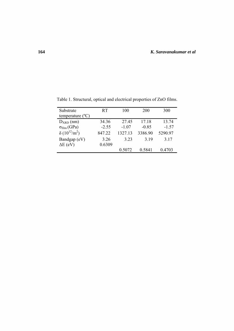
Table 1. Structural, optical and electrical properties of ZnO films.
Substrate temperature (ºC)
RT 100 200 300
DXRD (nm) 34.36 27.45 17.18 13.74 σfilm (GPa) -2.55 -1.07 -0.85 -1.57 δ (1012/m2) 847.22 1327.13 3386.90 5290.97 Bandgap (eV) 3.26 3.23 3.19 3.17 ΔE (eV) 0.6309
0.5072
0.5841
0.4703
XPS and Raman studies 165
Figure 1. XRD diffraction patterns of ZnO films grown on glass substrate for various temperatures.
166 K. Saravanakumar et al
Figure 2. Experimental Zn2p 3/ 2 and Zn2p 1/ 2 photoelectron peaks of ZnO films prepared at RT and 300ºC.

XPS and Raman studies 167
Figure 3. Expermental O1s photoelectron peak of ZnO films prepared at RT and 300ºC

168 K. Saravanakumar et al
Figure 4. Transmittance spectra of ZnO films grown under different substrate temperatures.
The inset in figure shows the linear extrapolation of band gap values of ZnO films.

XPS and Raman studies 169
Figure 5. Raman spectra of ZnO films grown at RT and 300ºC.

170 K. Saravanakumar et al
Figure 6. Variation of dc conductivity with substrate temperature. The inset in figure shows the variation of the resistivity as a function of the reciprocal of the temperature.
Received: December, 2010