xtr108evm-usb evaluation board and software tutorial · xtr108evm-usbevaluation board and software...
TRANSCRIPT

User's GuideSBOU123–March 2012
XTR108EVM-USB Evaluation Board and Software Tutorial
This user's guide describes the characteristics, operation and use of the XTR108EVM-USB evaluationmodule (EVM). This EVM is designed to evaluate the performance of the XTR108, an SPI™-programmable, current- or voltage-output, two-wire transmitter designed for temperature and bridgesensors. Throughout this document, the terms evaluation board, evaluation module, and EVM aresynonymous with the XTR108EVM-USB. This user's guide also includes information regarding operatingprocedures and input/output connections, an electrical schematic, printed circuit board (PCB) layoutdrawings, and a parts list for the EVM.
Contents1 Overview ..................................................................................................................... 42 Hardware Overview ......................................................................................................... 63 Hardware Setup ........................................................................................................... 164 Software Setup ............................................................................................................ 255 Software Overview ........................................................................................................ 266 General Operating Tips ................................................................................................... 477 Hardware Documentation ................................................................................................ 488 Appendix .................................................................................................................... 52
List of Figures
1 Hardware Included with the XTR108EVM-USB......................................................................... 5
2 XTR108EVM-USB Hardware Setup ...................................................................................... 6
3 XTR108EVM-USB Block Diagram ........................................................................................ 7
4 XTR108EVM-USB Interface Board Connectors and Jumpers ........................................................ 8
5 XTR108EVM-USB Sensor Board Connectors and Jumpers ........................................................ 13
6 Pin Socket Mechanical Description ..................................................................................... 16
7 Connecting the USB DAQ Platform to the XTR108EVM-USB Interface Board ................................... 17
8 All Boards Connected..................................................................................................... 17
9 Connecting Power to the USB DAQ Platform ......................................................................... 18
10 Connecting the USB Cable to the USB DAQ Platform ............................................................... 19
11 Found New Hardware Pop-up Message ............................................................................... 19
12 Connecting a Loop Power Supply to the XTR108EVM-USB Interface Board..................................... 20
13 34401A Multimeter Connections ........................................................................................ 21
14 USB DAQ Platform Default Jumper Settings .......................................................................... 22
15 XTR108EVM-USB Interface Board Default Jumper Settings........................................................ 23
16 XTR108EVM-USB Sensor Board Default Jumper Settings.......................................................... 24
17 Starting the XTR108EVM-USB Software............................................................................... 25
18 XTR108EVM-USB Software Start-up, Block Diagram Tab .......................................................... 26
19 USB Communication Error ............................................................................................... 27
20 XTR108EVM-USB Software, Find Resistors Tab ..................................................................... 32
21 RSET Error ................................................................................................................... 34
22 Linearity Warning .......................................................................................................... 34Windows is a trademark of Microsoft Corporation.SPI is a trademark of Motorola, Inc.All other trademarks are the property of their respective owners.
1SBOU123–March 2012 XTR108EVM-USB Evaluation Board and Software TutorialSubmit Documentation Feedback
Copyright © 2012, Texas Instruments Incorporated

www.ti.com
23 Save Model File ........................................................................................................... 35
24 XTR108EVM-USB Software, Manual Calibration Tab................................................................ 36
25 Adjust RTD Emulator...................................................................................................... 37
26 Manual Calibration Tab, Post-Calibration .............................................................................. 39
27 XTR108EVM-USB Software, Automatic Calibration Tab............................................................. 40
28 Automatic Calibration Tab, Post-Calibration ........................................................................... 42
29 XTR108EVM-USB Software, Registers Tab ........................................................................... 43
30 GPIO Control Window .................................................................................................... 45
31 Debug Window............................................................................................................. 46
32 About Window.............................................................................................................. 46
33 Discrete Charge Pump on Sensor Interface Board ................................................................... 47
34 XTR108EVM-USB Interface Board Schematic ........................................................................ 48
35 XTR108EVM-USB Sensor Board Schematic .......................................................................... 49
36 XTR108 Input MUX Example (TMIN = –200°C, PT100 RTD) ......................................................... 52
37 XTR108 Input MUX Example (TMAX = +850°C, PT100 RTD) ........................................................ 53
38 XTR108 Input MUX Example (TMAX = +850°C, PT1000 RTD) ....................................................... 53
39 RSET Circuitry ............................................................................................................... 54
40 RLIN Circuitry ................................................................................................................ 54
41 Linearity Correction Method.............................................................................................. 55
42 Linearity Improvement .................................................................................................... 55
List of Tables
1 XTR108EVM-USB Kit Contents........................................................................................... 5
2 Related Documentation .................................................................................................... 6
3 Multimeter Connect Pinout ................................................................................................ 9
4 J1 Pinout (15-Pin Female DSUB)......................................................................................... 9
5 J2 Pinout (Vo_XTR108) .................................................................................................... 9
6 J3 Pinout (Io_XTR108) ................................................................................................... 10
7 J4 Pinout (Loop Supply) .................................................................................................. 10
8 J5 Pinout (25-Pin Female DSUB) ....................................................................................... 10
9 J6 Pinout (25-Pin Male DSUB) .......................................................................................... 11
10 J7 Pinout (SPI)............................................................................................................. 11
11 J8 Pinout (RTD_CON) .................................................................................................... 12
12 Interface Board Jumper Functions ...................................................................................... 12
13 J1 Pinout (SPI)............................................................................................................. 14
14 J3 Pinout (Io_XTR108) ................................................................................................... 14
15 J4 Pinout (Vo_XTR108) .................................................................................................. 14
16 J5 Pinout (RTD_CON) .................................................................................................... 14
17 Sensor Board Jumper Functions ........................................................................................ 15
18 XTR108EVM-USB Interface Board Default Jumper Settings........................................................ 23
19 XTR108EVM-USB Sensor Board Default Jumper Settings.......................................................... 25
20 PGA Gain, Loop Transconductance, and Input Full-Scale Differential Voltage ................................... 28
21 Equations for Calculating Zero Output.................................................................................. 28
22 Equations for Calculating IREF Current .................................................................................. 29
23 Overscale Threshold ...................................................................................................... 30
24 Underscale Threshold..................................................................................................... 30
25 Alarm Configuration Register ............................................................................................ 31
26 Standard RTD Equations ................................................................................................. 33
27 Control Bits Functions .................................................................................................... 45
2 XTR108EVM-USB Evaluation Board and Software Tutorial SBOU123–March 2012Submit Documentation Feedback
Copyright © 2012, Texas Instruments Incorporated

www.ti.com
28 XTR108EVM-USB Interface Board Bill of Materials .................................................................. 50
29 XTR108EVM-USB Sensor Board Bill of Materials .................................................................... 51
30 Standard RTD Equations ................................................................................................. 56
31 Mnemonic Commands .................................................................................................... 59
32 SPI Modes of Operation .................................................................................................. 60
33 General USB-DAQ Commands.......................................................................................... 60
3SBOU123–March 2012 XTR108EVM-USB Evaluation Board and Software TutorialSubmit Documentation Feedback
Copyright © 2012, Texas Instruments Incorporated

Overview www.ti.com
1 Overview
This document provides the information needed to set up and operate the XTR108EVM-USB evaluationmodule, which is a test platform for the XTR108 programmable two-wire transmitter and sensorconditioner. For a more detailed description of the XTR108, refer to the product data sheet (SBOS187)available from the Texas Instruments web site at www.ti.com.
The XTR108EVM-USB is an evaluation module that is used to fully evaluate the XTR108. The XTR108 isan integrated circuit that provides correction of zero, span, and linearization errors for RTDs (resistivethermal devices) and bridge sensors. Overall system accuracy of 0.1% error (relative to full-scale outputspan) or less is easily achievable using a two-point calibration algorithm. The XTR108EVM-USB consistsof three PCBs. One board (the USB DAQ Platform) generates the digital signals required to communicatewith the XTR108. The second board (XTR108EVM-USB Interface Board) provides a convenient interfaceto standard multimeters and includes an onboard RTD emulator circuit to facilitate calibration. The thirdboard (XTR108EVM-USB Sensor Board) contains the XTR108 device as well as support andconfiguration circuitry. Once calibrated, the XTR108EVM-USB Sensor Board can be used as a fully-functional, stand-alone system. Similarly, the USB-DAQ Platform and XTR108EVM-USB Interface Boardcan be connected to other stand-alone XTR108 circuitry for quick calibration, making the XTR108EVM-USB a capable production tool.
4 XTR108EVM-USB Evaluation Board and Software Tutorial SBOU123–March 2012Submit Documentation Feedback
Copyright © 2012, Texas Instruments Incorporated

+6V Power Supply (wall-wart) USB Cable
USB DAQPlatform
XTR108EVM-USBInterface Board
XTR108EVM-USBSensor Board
www.ti.com Overview
1.1 XTR108EVM-USB Kit Contents
Figure 1 shows the hardware included with the XTR108EVM-USB kit. Table 1 describes each itemincluded in the kit. Contact the Texas Instruments Product Information Center nearest you if anycomponent is missing. It is highly recommended that you also check the XTR108 product folder to verifythat you have the latest version of the related software.
Figure 1. Hardware Included with the XTR108EVM-USB
Table 1. XTR108EVM-USB Kit Contents
Quantity Item Description
1 USB DAQ Platform Digital communications board
1 XTR108EVM-USB Interface Board XTR108EVM-USB Interface Board with required populated components
1 XTR108EVM-USB Sensor Board XTR108EVM-USB Sensor Board with required populated components
1 USB cable Connects PC to USB DAQ Platform
1 +6-V power supply (wall-wart) Provides power to USB DAQ Platform
1 Software installation disk Contains required software and documentation
5SBOU123–March 2012 XTR108EVM-USB Evaluation Board and Software TutorialSubmit Documentation Feedback
Copyright © 2012, Texas Instruments Incorporated
Windows PC HP/Agilent 34401A DMM
+24V Power Supply
USB Cable
+6V Power Supply
(wall-wart)
XTR108EVM-USB
Interface Board
XTR108EVM-USB
Sensor Board
USB-DAQ
Platform
HI(F) LO(F) HI(S) LO(S) I(F)
Hardware Overview www.ti.com
1.2 Related Documentation from Texas Instruments
The documents listed in Table 2 provide information regarding Texas Instruments' hardware used inassembly of the XTR108EVM-USB. This user's guide is available from the TI web site under literaturenumber SBOU123. Any letter appended to the literature number corresponds to the document revisionthat is current at the time of the writing of this document. Newer revisions may be available from the TIweb site at www.ti.com, or contact the Texas Instruments Product Information Center. Identify thedocument by both title and literature number.
Table 2. Related Documentation
Document Literature Number
USB DAQ Platform user's guide SBOU056
XTR108 product data sheet SBOS187
2 Hardware Overview
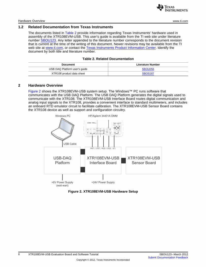
Figure 2 shows the XTR108EVM-USB system setup. The Windows™ PC runs software thatcommunicates with the USB DAQ Platform. The USB DAQ Platform generates the digital signals used tocommunicate with the XTR108. The XTR108EVM-USB Interface Board routes digital communication andanalog input signals to the XTR108, provides a convenient interface to standard multimeters, and includesan onboard RTD emulator circuit to facilitate calibration. The XTR108EVM-USB Sensor Board containsthe XTR108 device as well as support and configuration circuitry.
Figure 2. XTR108EVM-USB Hardware Setup
6 XTR108EVM-USB Evaluation Board and Software Tutorial SBOU123–March 2012Submit Documentation Feedback
Copyright © 2012, Texas Instruments Incorporated

XTR108EVM-USBInterface Board
XTR108EVM-USBSensor Board
25-pin DSUB from USB DAQ
25-pin DSUB from USB DAQ
15-pin DSUB
XTR108
RTDEmulator
Signal RoutingCircuit
Digital MultimeterInterface
External DeviceConnections
Control Signals
5.0V Power Supply
SPI Interface
EEPROM
Loop SupplyConnection
RTDConnection
Loop SupplySPI InterfaceRTD Emulator
External DeviceConnections
Current/Voltage Output
www.ti.com Hardware Overview
2.1 XTR108EVM-USB Theory of Operation
Figure 3 shows the block diagram of the XTR108EVM-USB Interface Board and Sensor Board.
Figure 3. XTR108EVM-USB Block Diagram
The XTR108EVM-USB Interface Board provides connections to the SPI interface and 5.0-V power supplyon the USB DAQ Platform and also provides a convenient interface to an external digital multimeter(DMM). The Interface Board also contains a network of signal-controlled relays from the USB DAQ thathandles the routing of all EVM input and output signals.
The Interface Board also includes a user-configurable RTD emulator circuit that simulates the behavior ofa RTD (resistive thermal device) using potentiometers and surface-mount resistors. Using the RTDemulator allows the user to more quickly achieve a deeper understanding of the XTR108EVM-USBhardware and software. When the XTR108EVM-USB capabilities and functions are fully understood, theuser can connect a real-world sensor to the EVM and perform a full calibration. Note that calibrations withreal-world sensors are time-consuming because devices such as these are normally calibrated at multipletemperatures in an environmental chamber. It is not unusual for temperature calibration to require 12hours.
The XTR108EVM-USB Sensor board contains the XTR108 device as well as support and configurationcircuitry. The configuration circuitry includes a 4Kb EEPROM used to store the XTR108 power-on settings.When the XTR108 is powered on it automatically reads the EEPROM and programs its internal registerswith the values stored in the EEPROM.
7SBOU123–March 2012 XTR108EVM-USB Evaluation Board and Software TutorialSubmit Documentation Feedback
Copyright © 2012, Texas Instruments Incorporated
Hardware Overview www.ti.com
2.2 Interface Board Overview
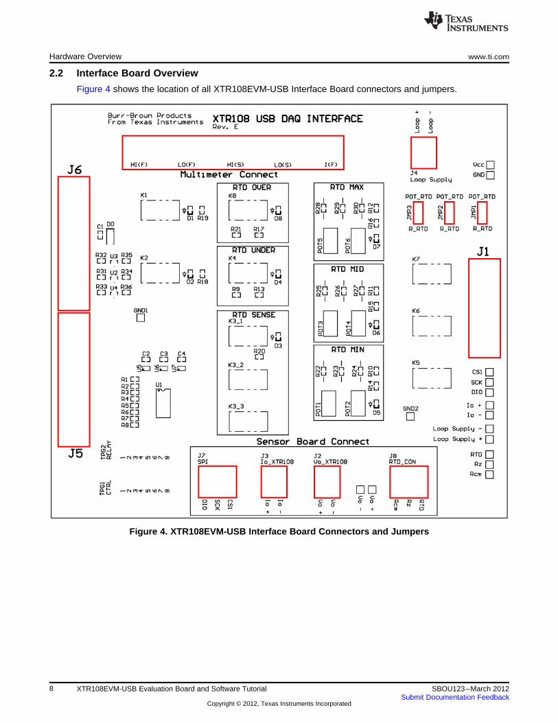
Figure 4 shows the location of all XTR108EVM-USB Interface Board connectors and jumpers.
Figure 4. XTR108EVM-USB Interface Board Connectors and Jumpers
8 XTR108EVM-USB Evaluation Board and Software Tutorial SBOU123–March 2012Submit Documentation Feedback
Copyright © 2012, Texas Instruments Incorporated

www.ti.com Hardware Overview
2.2.1 Interface Board: Signal Definitions and Pinouts
This section provides the signal definitions for all XTR108EVM-USB Interface Board connectors.
2.2.1.1 Multimeter Connect
Table 3 shows the signals connected to the Multimeter Connect interface on the Interface Board.
Table 3. Multimeter Connect Pinout
Name Description
HI(F) Voltage and resistance measurement; high-side forced connection
LO(F) Voltage and resistance measurement; low-side forced connection
HI(S) Voltage and resistance measurement; high-side sensed connection
LO(S) Voltage and resistance measurement; low-side sensed connection
I(F) Current output measurement connection
2.2.1.2 J1 (15-Pin Female DSUB)
Table 4 shows the signals connected to J1 on the Interface Board. J1 is the connection for all input andoutput signals between the Interface Board and Sensor Board.
Table 4. J1 Pinout (15-Pin Female DSUB)
Pin Name Description
1 SPI_DIO SPI data input/output
2 SPI_SCK SPI clock
3 SPI_CS1 SPI chip select
4 RCM RCM (common-mode resistor)
5 RZ RZ (zero-scale resistor)
6 RTD RTD resistance
7 IO– Low-side current output from the XTR108
8 IO+ High-side current output from the XTR108
9 VO– Low-side voltage output from the XTR108
10 VO+ High-side voltage output from the XTR108
11 GND Ground
12-15 NC No connection
2.2.1.3 J2 (Vo_XTR108)
Table 5 shows the signals connected to J2 on the Interface Board. J2 is used to connect the voltageoutput of an external XTR108 system to the Interface Board.
Table 5. J2 Pinout (Vo_XTR108)
Pin Name Description
1 VO+ High-side voltage output from the XTR108
2 VO– Low-side voltage output from the XTR108
9SBOU123–March 2012 XTR108EVM-USB Evaluation Board and Software TutorialSubmit Documentation Feedback
Copyright © 2012, Texas Instruments Incorporated

Hardware Overview www.ti.com
2.2.1.4 J3 (Io_XTR108)
Table 6 shows the signals connected to J3 on the Interface Board. J3 is used to connect the currentoutput of an external XTR108 system to the Interface Board.
Table 6. J3 Pinout (Io_XTR108)
Pin Name Description
1 IO+ High-side current output from the XTR108
2 IO– Low-side current output from the XTR108
2.2.1.5 J4 (Loop Supply)
Table 7 shows the signals connected to J4 on the Interface Board. J4 provides the loop power supply tothe XTR108.
Table 7. J4 Pinout (Loop Supply)
Pin Name Description
1 LOOP– Low-side loop power supply
2 LOOP+ High-side loop power supply
2.2.1.6 J5 (25-Pin Female DSUB)
Table 8 shows the signals connected to J5 on the Interface Board. J5 is used to connect the USB DAQcontrol signals to the Interface Board.
Table 8. J5 Pinout (25-Pin Female DSUB)
Pin Name Description Used
1 NC No connection No
2 CTRL1 Control signal 1 Yes
3 CTRL2 Control signal 1 Yes
4 CTRL3 Control signal 1 Yes
5 CTRL4 Control signal 1 Yes
6 CTRL5 Control signal 1 Yes
7 CTRL6 Control signal 1 Yes
8 CTRL7 Control signal 1 Yes
9 CTRL8 Control signal 1 Yes
10 MEAS1 Measure input 1 No
11 MEAS2 Measure input 1 No
12 MEAS3 Measure input 1 No
13 MEAS4 Measure input 1 No
14 MEAS5 Measure input 1 No
15 MEAS6 Measure input 1 No
16 MEAS7 Measure input 1 No
17 MEAS8 Measure input 1 No
18 SPI_SCK SPI clock, channel 2 No
19 SPI_CS2 SPI chip select, channel 2 No
20 SPI_DOUT2 SPI data output, channel 2 No
21 SPI_DIN2 SPI data input, channel 2 No
22 VDUT Switched power supply No
23 VCC USB DAQ power supply No
24, 25 GND Ground No
10 XTR108EVM-USB Evaluation Board and Software Tutorial SBOU123–March 2012Submit Documentation Feedback
Copyright © 2012, Texas Instruments Incorporated

www.ti.com Hardware Overview
2.2.1.7 J6 (25-Pin Male DSUB)
Table 9 shows the signals connected to J6 on the Interface Board. J6 is used to connect the SPI interfaceand 5.0-V power supply from the USB DAQ to the Interface Board.
Table 9. J6 Pinout (25-Pin Male DSUB)
Pin Name Description Used
1 DAC_A DAC_A output No
2 DAC_B DAC_B output No
3 DAC_C DAC_C output No
4 DAC_D DAC_D output No
5 ADS1_VIN+ ADS1 positive input No
6 ADS1_VIN– ADS1 negative input No
7 ADS2_VIN+ ADS2 positive input No
8 ADS2_VIN– ADS2 negative input No
9 I2C_SCK I2C clock No
10 I2C_SDA I2C data No
11 ONE_WIRE One-wire communication line No
12 I2C_SDA_ISO I2C data (isolated) No
13 I2C_SCK_ISO I2C clock (isolated) No
14 XTR +LOOP Current-loop high-side input No
15 XTR –LOOP Current-loop low-side input No
16 INA– INA negative input No
17 VDUT Selectable 3.3-V or 5.0-V power supply No
18 VCC 5.0-V power supply Yes
19 +15V +15-V power supply No
20 –15V –15-V power supply No
21 GND Ground Yes
22 SPI_SCK SPI clock, channel 1 Yes
23 SPI_CS1 SPI chip select, channel 1 Yes
24 SPI_DOUT SPI data output, channel 1 Yes
25 SPI_DIN1 SPI data input, channel 1 Yes
2.2.1.8 J7 (SPI)
Table 10 shows the signals connected to J7 on the Interface Board. J7 is used to connect the SPIinterface to an external XTR108 system.
Table 10. J7 Pinout (SPI)
Pin Name Description
1 DIO SPI data input/output
2 SCK SPI clock
3 CS1 SPI chip select
11SBOU123–March 2012 XTR108EVM-USB Evaluation Board and Software TutorialSubmit Documentation Feedback
Copyright © 2012, Texas Instruments Incorporated

Hardware Overview www.ti.com
2.2.1.9 J8 (RTD_CON)
Table 11 shows the signals connected to J8 on the Interface Board. J8 is used to connect the RTDemulator circuit to an external XTR108 system.
Table 11. J8 Pinout (RTD_CON)
Pin Name Description
1 RCM RCM (common-mode resistor)
2 RZ RZ (zero-scale resistor)
3 RTD RTD resistance
2.2.2 Interface Board Jumper Settings
Table 12 explains the function of the XTR108EVM-USB Interface Board jumpers.
Table 12. Interface Board Jumper Functions
Jumper Default Description
This jumper selects which resistor string is used for the RTD emulator minimum-scale output.Set the jumper to the POT_RTD position to use potentiometers POT1 and POT2. Set theJMP1 POT_RTD jumper to the R_RTD position to use surface-mount resistors R22-R24 (not installed bydefault).
This jumper selects which resistor string is used for the RTD emulator mid-scale output.Set the jumper to the POT_RTD position to use potentiometers POT3 and POT4. Set theJMP2 POT_RTD jumper to the R_RTD position to use surface-mount resistors R25-R27 (not installed bydefault).
This jumper selects which resistor string is used for the RTD emulator maximum-scale output.Set the jumper to the POT_RTD position to use potentiometers POT5 and POT6. Set theJMP3 POT_RTD jumper to the R_RTD position to use surface-mount resistors R28-R30 (not installed bydefault).
12 XTR108EVM-USB Evaluation Board and Software Tutorial SBOU123–March 2012Submit Documentation Feedback
Copyright © 2012, Texas Instruments Incorporated

www.ti.com Hardware Overview
2.3 Sensor Board Overview
Figure 5 shows the location of all XTR108EVM-USB Sensor Board connectors and jumpers.
Figure 5. XTR108EVM-USB Sensor Board Connectors and Jumpers
13SBOU123–March 2012 XTR108EVM-USB Evaluation Board and Software TutorialSubmit Documentation Feedback
Copyright © 2012, Texas Instruments Incorporated

Hardware Overview www.ti.com
2.3.1 Sensor Board Connections
This section provides signal definitions for all XTR108EVM-USB Interface Board connectors.
2.3.1.1 J1 (SPI)
Table 13 shows the signals connected to J1 on the Sensor Board. J1 is used to connect an external SPIinterface to the Sensor Board.
Table 13. J1 Pinout (SPI)
Pin Name Description
1 CS1 SPI chip select
2 SCK SPI clock
3 SDIO SPI data input/output
2.3.1.2 J2 (15-pin Male DSUB)
J2 is the connection for all input and output signals between the Interface Board and Sensor Board. SeeTable 4 for pinout information.
2.3.1.3 J3 (Io_XTR108)
Table 14 shows the signals connected to J3 on the Sensor Board. J3 is used to connect an external looppower supply to the Sensor Board and to connect the XTR108 current output to an external ammeter.
Table 14. J3 Pinout (Io_XTR108)
Pin Name Description
1 IO– Low-side loop power-supply and current output from the XTR108
2 IO+ High-side loop power-supply and current output from the XTR108
2.3.1.4 J4 (Vo_XTR108)
Table 15 shows the signals connected to J4 on the Sensor Board. J4 is used to connect the XTR108voltage output to an external voltmeter.
Table 15. J4 Pinout (Vo_XTR108)
Pin Name Description
1 VO+ High-side voltage output from the XTR108
2 VO– Low-side voltage output from the XTR108
2.3.1.5 J5 (RTD_CON)
Table 16 shows the signals connected to J5 on the Sensor Board. J5 is used to connect an external RTDto the Sensor Board.
Table 16. J5 Pinout (RTD_CON)
Pin Name Description
1 RTD RTD resistance. Connect the red wire of a two- or three-wire RTD here.
2 RZ RZ (zero-scale resistor). Connect the black wire of a two- or three-wire RTD here.
RCM (common-mode resistor). Short to pin 2 (RZ) if using a two-wire RTD. Connect the second3 RCM black wire here if using a three-wire RTD.
14 XTR108EVM-USB Evaluation Board and Software Tutorial SBOU123–March 2012Submit Documentation Feedback
Copyright © 2012, Texas Instruments Incorporated

www.ti.com Hardware Overview
2.3.2 Sensor Board Jumper Settings
Table 17 explains the function of the XTR108EVM-USB Interface Board jumpers.
Table 17. Sensor Board Jumper Functions
Jumper Default Description
This jumper selects whether to enable or bypass the depletion-mode transistor Q1.JMP1 FET Set the jumper to the FET position when using current-output mode. Set the jumper to the
BYPASS position when using voltage-output mode.
This jumper selects whether to enable or bypass the depletion-mode transistor Q1.JMP2 FET Set the jumper to the FET position when using current-output mode. Set the jumper to the
BYPASS position when using voltage-output mode.
This jumper selects between current-output mode or voltage-output mode.JMP3 IOUT Set the jumper to the IOUT position when using current-output mode. Set the jumper to the
VOUT position when using voltage-output mode.
This jumper selects whether to connect or disconnect a load resistor (RL, not installed bydefault) from the voltage output of the XTR108.JMP4 NO LOAD Set the jumper to the NO LOAD position when using current-output mode. Set the jumper tothe LOAD position when using voltage-output mode (optional).
This jumper selects between the current-output or voltage-mode charge pump input at theXTR108 I_IN pin.JMP5 IOUT Set the jumper to the IOUT position when using current-output mode. Set the jumper to theCP position when using voltage-output mode.
This jumper enables or disables the SPI clock buffer in the voltage-output mode charge pump.JMP6 BYPASS Set the jumper to the BYPASS position when using current-output mode. Set the jumper to
the BUF position when using voltage-output mode.
This jumper enables or disables the voltage-output mode charge pump.JMP7 NO CLK Set the jumper to the NO CLK position when using current-output mode. Set the jumper to the
CP SCK position when using voltage-output mode.
This jumper selects what type of RTD is connected to the XTR108.Set the jumper to the 2-WIRE position when using the RTD emulator on the Interface BoardJMP8 2-WIRE or when connecting an external two-wire RTD. Set the jumper to the 3-WIRE position whenconnecting an external three-wire RTD.
15SBOU123–March 2012 XTR108EVM-USB Evaluation Board and Software TutorialSubmit Documentation Feedback
Copyright © 2012, Texas Instruments Incorporated

Through-hole lead
makes contact to
pin socket with
spring action.
PIN DIA0.36 - 0.56
[.014 - .022]
SPRING
EYELET
6.60
[.260]
2.54
[.100]
CONTACT PT
MIN
6.27
[.247] MAX PIN LENGTH
Hardware Setup www.ti.com
2.3.3 Test Points and Miscellaneous Breadboard Area
There are multiple points available on the Sensor Board, including several connections to IRET. IRET iscommon (labeled as GND on the board) for most XTR108 applications, and is provided for ease ofmeasuring analog signals. Reserved areas with plated-through, standard-spacing, 0.1-inch holes formiscellaneous proof-of-concept breadboarding are also provided on the board. Most of the surface-mountcomponents have pin sockets associated with them. These pin sockets allow the replacement of asurface-mount component with a through-hole component.
The pin sockets provide good contact with the leads of a component without solder, thus enabling quickreconfiguration of the board for many different XTR108 designs, as shown in Figure 6.
Figure 6. Pin Socket Mechanical Description
3 Hardware Setup
The XTR108EVM-USB hardware setup involves connecting the three EVM boards together, applyingpower to the USB DAQ platform, connecting the USB cable, applying power to the Interface Board, andsetting the jumpers. This section covers the details of this procedure.
3.1 Electrostatic Discharge Warning
CAUTION
Many of the components on the XTR108EVM-USB are susceptible to damageby electrostatic discharge (ESD). Customers are advised to observe properESD handling precautions when unpacking and handling the EVM, includingthe use of a grounded wrist strap at an approved ESD workstation.
16 XTR108EVM-USB Evaluation Board and Software Tutorial SBOU123–March 2012Submit Documentation Feedback
Copyright © 2012, Texas Instruments Incorporated

www.ti.com Hardware Setup
3.2 Connecting the Hardware
When first setting up the EVM hardware, It is recommended to first connect the USB DAQ Platform to theXTR108EVM-USB Interface Board. To connect the two PCBs together, gently push on both sides of the25-pin D-SUB connectors as shown in Figure 7. Make sure that the connectors are completely pushedtogether because loose connections may cause intermittent operation.
Figure 7. Connecting the USB DAQ Platform to the XTR108EVM-USB Interface Board
Next, connect the XTR108EVM-USB Sensor Board to the XTR108EVM-USB Interface Board by gentlypushing on both sides of the 15-pin DSUB connector. Once the XTR108EVM-USB Sensor Board isconnected, the system looks like the one in Figure 8.
Figure 8. All Boards Connected
17SBOU123–March 2012 XTR108EVM-USB Evaluation Board and Software TutorialSubmit Documentation Feedback
Copyright © 2012, Texas Instruments Incorporated

Connect +6V Power Supply to J5
µC OK, 3.3v, and VCC LEDs illuminated
Hardware Setup www.ti.com
3.3 Connecting Power and USB to the USB DAQ Platform
After the three XTR108EVM-USB parts are connected, connect the included 6-V power supply (wall-wart)to terminal J5 of the USB DAQ platform. If connected properly, the µC OK, 3.3-V, and VCC LEDs on theUSB DAQ illuminate as shown in Figure 9. Always connect power before connecting the USB cable. If youconnect the USB cable before connecting the power, the computer attempts to communicate with anunpowered device that is unable to respond.
Figure 9. Connecting Power to the USB DAQ Platform
18 XTR108EVM-USB Evaluation Board and Software Tutorial SBOU123–March 2012Submit Documentation Feedback
Copyright © 2012, Texas Instruments Incorporated

www.ti.com Hardware Setup
Once power has been applied to the USB DAQ Platform, you can connect one end of the USB cable tothe USB DAQ and the other end to a PC USB port, as shown in Figure 10. Figure 11 shows the typicalresponse to connecting the USB DAQ Platform to a PC USB port for the first time. Typically, the computerresponds with a Found New Hardware, USB Device pop-up message. The pop-up message typicallychanges to Found New Hardware, USB Human Interface Device shortly after. This message indicatesthat the device is ready to be used. The USB DAQ Platform uses the Human Interface Device drivers thatare part of the Microsoft® Windows® operating system.
In some cases, the Windows Add Hardware Wizard pops up. If this prompt occurs, allow the systemdevice manager to install the Human Interface Device drivers by clicking Yes when requested to install thedrivers.
Figure 10. Connecting the USB Cable to the USB DAQ Platform
Figure 11. Found New Hardware Pop-up Message
19SBOU123–March 2012 XTR108EVM-USB Evaluation Board and Software TutorialSubmit Documentation Feedback
Copyright © 2012, Texas Instruments Incorporated

Connect DC Lab Power Supply to J4
IOUT Mode: 12V to 24VVOUT Mode: 3V to 5.5V
Hardware Setup www.ti.com
3.4 Connecting Loop Power Supply to the XTR108EVM-USB Interface Board
Connect a dc lab power supply to J4 on the Interface Board as shown in Figure 12. When operating incurrent-output mode, the loop-supply input voltage range is 12 V to 24 V. In general, you must considerthe power dissipated in the external transistor and the operating temperature of the transistor in order todetermine the maximum loop voltage and current. This calculation is determined in the XTR108 datasheet. When operating in voltage-output mode, the loop-supply input voltage range is (3.0 V to 5.5 V) +VD1.
Figure 12. Connecting a Loop Power Supply to the XTR108EVM-USB Interface Board
20 XTR108EVM-USB Evaluation Board and Software Tutorial SBOU123–March 2012Submit Documentation Feedback
Copyright © 2012, Texas Instruments Incorporated

Connect to HI (F)
Connect to HI (S)
Connect to LO (F)
Connect to LO (S)
Connect to I (F)
www.ti.com Hardware Setup
3.5 Connecting Outputs to a Digital Multimeter (DMM)
The XTR108EVM-USB contains circuitry that routes the current output, voltage output, and RTD emulatorsignals to the multimeter connect terminals on the XTR108EVM-USB Interface Board. Any standard labmultimeter that supports dc voltage, dc current, and four-wire resistance measurements is compatible withthe XTR108EVM-USB. This EVM is designed and tested with the Agilent 34401A multimeter.
To properly connect the XTR108EVM-USB Interface Board to the 34401A multimeter, follow theinstructions given in Figure 13. Use the same connections for any other compatible multimeter.
Figure 13. 34401A Multimeter Connections
21SBOU123–March 2012 XTR108EVM-USB Evaluation Board and Software TutorialSubmit Documentation Feedback
Copyright © 2012, Texas Instruments Incorporated

Hardware Setup www.ti.com
3.6 USB DAQ Platform Default Jumper Settings
Figure 14 shows the default USB DAQ Platform jumper configuration. In general, these jumpers shouldnot be changed. For more information about the function of these jumpers, refer to the USB DAQ PlatformUser's Guide.
Figure 14. USB DAQ Platform Default Jumper Settings
22 XTR108EVM-USB Evaluation Board and Software Tutorial SBOU123–March 2012Submit Documentation Feedback
Copyright © 2012, Texas Instruments Incorporated

www.ti.com Hardware Setup
3.7 XTR108EVM-USB Interface Board Default Jumper Settings
Figure 15 shows the default XTR108EVM-USB Interface Board jumper configuration. Table 18summarizes the default jumper configuration. For more information about the jumpers on the InterfaceBoard, see Table 12.
Figure 15. XTR108EVM-USB Interface Board Default Jumper Settings
Table 18. XTR108EVM-USB Interface Board Default Jumper Settings
Jumper Position Description
JMP1 POT_RTD Use POT1, POT2 for the RTD emulator minimum-scale output
JMP2 POT_RTD Use POT3, POT4 for the RTD emulator mid-scale output
JMP3 POT_RTD Use POT5, POT6 for the RTD emulator maximum-scale output
23SBOU123–March 2012 XTR108EVM-USB Evaluation Board and Software TutorialSubmit Documentation Feedback
Copyright © 2012, Texas Instruments Incorporated

Hardware Setup www.ti.com
3.8 XTR108EVM-USB Sensor Board Default Jumper Settings
Figure 16 shows the default XTR108EVM-USB Sensor Board jumper configuration. Table 19 summarizesthe default jumper configuration. For more information about the jumpers on the Sensor Board, seeTable 17.
Figure 16. XTR108EVM-USB Sensor Board Default Jumper Settings
24 XTR108EVM-USB Evaluation Board and Software Tutorial SBOU123–March 2012Submit Documentation Feedback
Copyright © 2012, Texas Instruments Incorporated

www.ti.com Software Setup
Table 19. XTR108EVM-USB Sensor Board Default Jumper Settings
Jumper Position Description
JMP1 FET Enable FET sub regulator
JMP2 FET Enable FET sub regulator
JMP3 IOUT Current-output mode
JMP4 NO LOAD Load resistor disconnected
JMP5 IOUT Current-output mode
JMP6 BYPASS Bypass SPI clock buffer on charge pump
JMP7 NO CLK Disable charge pump
JMP8 2-WIRE Select two-wire RTD
4 Software Setup
This section describes how to install the XTR108EVM-USB software.
4.1 Operating Systems for XTR108EVM-USB Software
The XTR108EVM-USB software is tested on the Microsoft Windows XP operating system (OS) withUnited States and European regional settings. The software should also function on other Windowsoperating systems. Please report any OS compatibility issues to the Precision Amplifiers E2E forum.
4.2 XTR108EVM-USB Software Installation
Follow these steps to install the XTR108EVM-USB software:
1. Software can be downloaded from the XTR108EVM-USB product folder, or from the disk included withthe XTR108EVM-USB that includes a folder called Install_software/.
2. Find the file called setup.exe. Double-click the file to start the installation process.
3. Follow the on-screen prompts to install the software.
4. To remove the application, use the Windows Add/Remove Software control panel utility.
4.3 Starting the XTR108EVM-USB Software
The XTR108EVM-USB software can be started through the Windows Start menu. Click Start → AllPrograms → XTR108EVM-USB → XTR108EVM-USB to start the program, as shown in Figure 17.
Figure 17. Starting the XTR108EVM-USB Software
25SBOU123–March 2012 XTR108EVM-USB Evaluation Board and Software TutorialSubmit Documentation Feedback
Copyright © 2012, Texas Instruments Incorporated

Software Overview www.ti.com
5 Software Overview
Once the XTR108EVM-USB starts up, several SPI communications take place to initialize the InterfaceBoard and read the XTR108 register values. Refer to Figure 18 for a screen shot of how the softwareshould appear if the EVM is functioning properly. The actual values of the fields inside the XTR108 blockdiagram (such as PGA gain or ILIN DAC Linearization) may vary.
Figure 18. XTR108EVM-USB Software Start-up, Block Diagram Tab
26 XTR108EVM-USB Evaluation Board and Software Tutorial SBOU123–March 2012Submit Documentation Feedback
Copyright © 2012, Texas Instruments Incorporated

www.ti.com Software Overview
If there is an error in the communication between the PC and the USB-DAQ, an error message pops upas shown in Figure 19. In this case, it is recommended to close the EVM software, disconnect the powerand USB cables from the USB-DAQ, and wait a few moments. Next reconnect the power cable, thenreconnect the USB cable. After a few moments, start the XTR108EVM-USB software again.
Figure 19. USB Communication Error
5.1 Block Diagram Tab
The Block Diagram tab shown in Figure 18 is loaded by default during the XTR108EVM-USB softwarestart-up. This tab primarily serves to display the XTR108 register values in a way that is easy to interpretbecause nearly every register hexadecimal value is converted to the real-world setting that the registerrepresents. Other indicators display the supporting circuitry values for the current configuration. Theremainder of this section provides an in-depth explanation of the function of each group of controls andindicators in the Block Diagram tab. All fields located internal to the XTR108 are controls that can bemanipulated by the user, but it is recommended that only advanced users make changes to the controls inthe Block Diagram tab.
For more information about any of the circuitry mentioned in the Block Diagram Tab section, see theTheory of Operation section in the XTR108 data sheet.
5.1.1 Input MUX
The Input MUX section of the block diagram shows the connections for the RTD sensor, zero-scaleresistors (RZ1 through RZ5), and common-mode resistor (RCM). This section also displays the XTR108 inputmultiplexer settings. The multiplexer controls which input channels are connected to the excitation currentsources and the input PGA. The default setting for the multiplexer is to connect the excitation currentsource (IREF2) and PGA input (VIN+) to input channel V/I-0 (RTD channel) and to connect the excitationcurrent source (IREF1) and PGA input (VIN–) to input channel V/I-1.
27SBOU123–March 2012 XTR108EVM-USB Evaluation Board and Software TutorialSubmit Documentation Feedback
Copyright © 2012, Texas Instruments Incorporated

VZERO = VZ_PROGRAM + VZ_COARSE + VZ_FINE50*APGA*IREF*(RTDMIN - RZ)
RVIIZERO = IOUT_MIN -
VZ_PROGRAM = 83.5 VREF IZ_PROGRAM = 8 RVI
175 VREF
VZ_COARSE = 80VREF
4N13 IZ_COARSE = 8 RVI
5 VREF
4N13
VZ_FINE = 80VREF
64N12 IZ_FINE = 8 RVI
5 VREF
64N12
Software Overview www.ti.com
5.1.2 PGA
The differential input voltage created by the current sources IREF1 and IREF2 flowing through the RTD and RZ
resistances is applied to the input pins of a programmable-gain instrumentation amplifier (PGA). The PGAhas seven voltage-gain settings in binary steps from 6.25 V/V to 400 V/V. The input common-mode rangeof the PGA is 0.2 V to 3.5 V above the IRET potential.
For common applications that require a 4-mA to 20-mA transmission, the PGA output voltage rangeshould be set to VZERO = 0.5 V and VFS = 2.5 V. Connecting an external voltage-to-current resistor (RVI =6.34 kΩ) between pin 9 (VO) and pin 10 (IIN) converts this voltage to a current that passes to the 50-A/Afixed-gain output current amplifier which produces a 4-mA to 20-mA output. In this mode, the PGA voltagegain converts to an overall transconductance in the range of 50 mA/V to 3200 mA/V (approximately).Table 20 shows the gain to transconductance relationship. For voltage-output applications, the PGA canbe set for rail-to-rail output (for example, VZERO = 0.5 V and VFS = 4.5 V). The PGA section of the blockdiagram shows the PGA voltage gain setting in V/V.
Table 20. PGA Gain, Loop Transconductance, and Input Full-Scale Differential Voltage
Voltage Gain Output Transconductance Full-Scale Differential VIN(V/V) (mA/V) (mV)
6.25 49 320
12.5 99 160
25 197 80
50 394 40
100 789 20
200 1577 10
400 3155 5
5.1.3 I_ZERO DAC
The zero-output level of the XTR108 input PGA is controlled by two DACs (coarse and fine). These digital-to-analog converters (DACs) compensate for the initial offset at the PGA input as a result of sensor andresistor mismatches as well as sensor non-idealities. Both the coarse and fine DAC are bidirectional(positive or negative) and allow the output level to be set above or below a preset pedestal. The equationsthat define the output of these DACs are given in Table 21. Note that the external resistor RVI (voltage-to-current conversion resistor) is used to convert the DAC reference voltage (VREF) into a current. The IZERO
DAC section of the block diagram shows the value of the coarse and fine zero-scale output DACs.
Table 21. Equations for Calculating Zero Output (1)
Voltage Referred to VO PinDAC Output with Respect to IRET Current Referred to IOUT Pin
Overall
Program
Coarse DAC
Fine DAC
(1) N13 and N12 are the decimal values of registers 13 and 12, respectively.
28 XTR108EVM-USB Evaluation Board and Software Tutorial SBOU123–March 2012Submit Documentation Feedback
Copyright © 2012, Texas Instruments Incorporated

IREF1,2 = IREF_PROGRAM + IREF_COARSE + IREF_FINE
IREF_PROGRAM = RSET
5 VREF
IREF_COARSE = RSET
VREF
64N11
IREF_FINE = RSET
VREF
1024N10
www.ti.com Software Overview
5.1.4 I_REF DAC
The XTR108 contains two matched, adjustable, reference current sources for sensor excitation. Eachcurrent source is controlled by a coarse DAC and fine DAC that together adjust the overall output. Theequations that define the output of these current sources are given in Table 22. Note that the externalresistor (RSET) is used to convert the DAC reference voltage (VREF) into the reference current. The IREF DACsection of the block diagram shows the values of the coarse and fine excitation current DACs and thevalue of RSET (current set resistor).
Table 22. Equations for Calculating IREF Current (1)
Current Source Output Reference Current
Overall
Program
Coarse DAC
Fine DAC
(1) N11 and N10 are the decimal values of registers 11 and 10, respectively.
5.1.5 I_LIN DAC
The XTR108 incorporates circuitry for correcting second-order RTD sensor nonlinearity by up to a 40:1ratio. To achieve this, a current is added to the sensor excitation current (IREF) that is proportional to thevoltage at the PGA input. The current is scaled by the linearization DAC (ILIN) that uses the externalresistor (RLIN) to convert voltage into current. The ILIN DAC section of the block diagram shows thehexadecimal value of the linearization register (register 14). The recommended value for the externalresistor RLIN is also shown at the bottom of the block diagram.
5.1.6 Overscale/Underscale
The XTR108 incorporates circuitry to set adjustable limits at the output in cases when the sensor signalgoes above or below the specified range. The circuit is designed for compliance with the NAMUR NE43recommendation for sensor interfaces. There are 16 levels for overscale output adjustment and eightlevels for underscale output adjustment. The limit levels are listed in Table 23 and Table 24, including thesettings of bits in the over- and underscale register (register 5) that are required for each step. Because ofthe large step sizes, units that use this feature should be checked if the value is critical. Note that theunderscale limit circuit overrides the IZERO DAC level if it is set lower and if there is not enough sensoroffset at the PGA input.
It may be necessary to disable limiting if the XTR108 is used in applications other than a 4-mA to 20-mAtransmitter (such as voltage-output mode) where the PGA output is between 0.5 V and 4.5 V. Theoverscale and underscale section of the block diagram shows whether overscale and underscale limitingis enabled or disabled as well as the current overscale and underscale output levels. These indicators areset by the values read from the XTR108 registers and EEPROM, not by the values selected in the FindResistors tab in the EVM software.
29SBOU123–March 2012 XTR108EVM-USB Evaluation Board and Software TutorialSubmit Documentation Feedback
Copyright © 2012, Texas Instruments Incorporated

Software Overview www.ti.com
Table 23. Overscale Threshold
IO OverscaleVO Overscale Threshold
OS3 OS2 OS1 OS0 Threshold RVI = 6.34 kΩ0 0 0 0 2.625 V 20.7 mA
0 0 0 1 2.6875 V 21.2 mA
0 0 1 0 2.75 V 21.7 mA
0 0 1 1 2.8125 V 22.2 mA
0 1 0 0 2.875 V 22.7 mA
0 1 0 1 2.9375 V 23.2 mA
0 1 1 0 3.0 V 23.7 mA
0 1 1 1 3.0625 V 24.2 mA
1 0 0 0 3.125 V 24.6 mA
1 0 0 1 3.1875 V 25.1 mA
1 0 1 0 3.25 V 25.6 mA
1 0 1 1 3.3125 V 26.1 mA
1 1 0 0 3.375 V 26.6 mA
1 1 0 1 3.4375 V 27.1 mA
1 1 1 0 3.5 V 27.6 mA
1 1 1 1 3.5625 V 28.1 mA
Table 24. Underscale Threshold
IO UnderscaleVO Underscale Threshold
US2 US1 US0 Threshold RVI = 6.34 kΩ0 0 0 450 mV 3.55 mA
0 0 1 425 mV 3.35 mA
0 1 0 400 mV 3.15 mA
0 1 1 375 mV 2.96 mA
1 0 0 350 mV 2.76 mA
1 0 1 325 mV 2.56 mA
1 1 0 300 mV 2.37 mA
1 1 1 275 mV 2.17 mA
30 XTR108EVM-USB Evaluation Board and Software Tutorial SBOU123–March 2012Submit Documentation Feedback
Copyright © 2012, Texas Instruments Incorporated

www.ti.com Software Overview
5.1.7 SPI Interface
In normal operation, the XTR108 reads data from an external EEPROM to retrieve calibrated registersettings. This operation is accomplished by a read-back controller on the XTR108. The read-backcontroller defaults to being active when the XTR108 is powered on and is continuously active unlessdisabled. In other words, it starts a new read operation as soon as the previous operation is completed. Acontrol bit (RBD) in Control Register 2 (register 4) is provided to allow the XTR108 to read the EEPROMonce and then stop.
When calibrating the XTR108EVM-USB, it is required that the automatic EEPROM read-back be disabled,so that new values written to the XTR108 registers during the calibration procedure are not immediatelyoverwritten. The calibration functions built into the XTR108EVM-USB software also write new registervalues to the EEPROM so that post-calibrated values are automatically loaded at power-up. The SPIInterface section of the block diagram shows whether the automatic EEPROM read-back is enabled ordisabled.
5.1.8 Alarm Config
The XTR108 Alarm Configuration register (register 7) determines whether the XTR108 goes overscale orunderscale for various detected fault conditions at the PGA input. Table 25 defines the behavior of thesesettings. If a bit corresponding to the particular error is set to '1', the output goes overscale when the erroroccurs. If a bit corresponding to the particular error is set to '0', the output goes underscale when the erroroccurs. The Alarm Config section of the block diagram shows the hexadecimal value of the AlarmConfiguration register.
Table 25. Alarm Configuration Register (1)
BIT AC7 AC6 AC5 AC4 AC3 AC2 AC1 AC0
VINN High Low Low High N N Low High
VINP Low High Low High Low High N N(1) A high reading indicates that the input exceeds the positive common-mode range; a low reading indicates that the input exceeds
the negative common-mode range; and N indicates that the input is within the common-mode range.
31SBOU123–March 2012 XTR108EVM-USB Evaluation Board and Software TutorialSubmit Documentation Feedback
Copyright © 2012, Texas Instruments Incorporated

Software Overview www.ti.com
5.2 Find Resistors Tab
The Find Resistors tab in the XTR108EVM-USB software allows the user to enter the desired XTR108operating conditions. Based on the user input, the software calculates the appropriate values for thesupporting circuitry and performs error-checking to determine if the desired conditions exceed systemcapabilities. This tab also allows the user to save a custom configuration as a model file that is used asthe basis for calibration.
Figure 20 shows the Find Resistors tab with default values. The following sections explain the use ofeach section of the tab.
Figure 20. XTR108EVM-USB Software, Find Resistors Tab
32 XTR108EVM-USB Evaluation Board and Software Tutorial SBOU123–March 2012Submit Documentation Feedback
Copyright © 2012, Texas Instruments Incorporated

www.ti.com Software Overview
5.2.1 Step 1: Enter Operating Conditions
This area of the Find Resistors tab allows the user to input system operating conditions, including theglobal system conditions as well as individual conditions for each channel. Global conditions consist ofcurrent- or voltage-output mode, output span, and overscale and underscale limiting. Channel-specificconditions include channel enable or disable, temperature span, RTD type, and Callendar-van Dusen(CVD) coefficients.
5.2.1.1 Mode
This control allows the user to select current-output mode or voltage-output mode. Ensure that the properpower-supply voltage is applied for each mode (see the Connecting Loop Power Supply to theXTR108EVM-USB Interface Board section) and that the correct Sensor Board jumper settings are used(see Table 17).
5.2.1.2 Output Span
This control allows the user to set the desired XTR108 output span. The most common output spansettings are 4 mA to 20 mA for current-output mode and 0.5 V to 4.5 V for voltage-output mode. Thesecontrols automatically update the units (mA or V) to reflect the status of the Mode control.
5.2.1.3 Overscale and Underscale
This control allows the user to enable or disable overscale and underscale limiting as well as set theoverscale and underscale output levels. The current and voltage levels available in the overscale andunderscale output controls correspond to the values listed in Table 23 and Table 24. These controlsautomatically update the units (mA or V) to reflect the status of the Mode control.
5.2.1.4 Channel Enable
The XTR108 supports up to five input channel configurations, allowing the same board design to be usedfor multiple input conditions. Only one channel can be calibrated at a time. The Channel Enable controlallows the user to enable or disable the five input channels, as required by their application.
5.2.1.5 Temperature
This control allows the user to input the minimum and maximum RTD temperature of each input channelin °C. The lowest possible minimum temperature is –200°C and the highest possible maximumtemperature is +850°C and matches the operating temperature ranges of most commercially-availableRTDs.
5.2.1.6 RTD Type
The XTR108 is primarily designed to interface to PT100- and PT1000-type RTDs. PT100 RTDs have aresistance of 100 Ω at 0°C; PT1000 RTDs have a resistance of 1000 Ω (1 kΩ) at 0°C. The RTD Typecontrol allows the user to specify what type of RTD is used at each input channel.
5.2.1.7 CVD Coefficients
The resistance of an RTD across its temperature range is defined by a set of polynomial equations, asshown in Table 26. A, B, and C are known as Callendar-van Dusen (CVD) coefficients. The industry-standard values for A, B, and C are loaded into the XTR108EVM-USB software by default, but customvalues for each channel can be entered in the CVD Coefficients control. The Reset CVD Coefficientsbutton restores the default values when clicked.
Table 26. Standard RTD Equations (1)
If –200°C < T < 0°C If T > 0°C
Rt = R0 [1 + A × T + B × T2 + C × T3(T – 100°C)] Rt = R0 [1 + A × T + B × T2](1) A = 3.9083E-3, B = –5.775E-7, C = –4.183E-12, R0 = RTD value at 0°C (typically 100 Ω or 1 kΩ), and T = temperature in °C.
33SBOU123–March 2012 XTR108EVM-USB Evaluation Board and Software TutorialSubmit Documentation Feedback
Copyright © 2012, Texas Instruments Incorporated

Software Overview www.ti.com
5.2.2 Step 2: Calculate Resistor Values
When the Calculate Resistors button is clicked, the XTR108EVM-USB software uses the operatingconditions entered in Step 1: Enter Operating Commands to calculate the best values for RSET, RLIN, RCM,and RZ (for each enabled channel).
The RSET value is critical to proper XTR108 operation (see the I_REF DAC section). If the software cannotfind a suitable RSET value, an error message is displayed as shown in Figure 21. This error is typicallycaused by narrow or conflicting temperature ranges on multiple channels. If you encounter this error,widen your temperature ranges slightly and click the Calculate Resistors button again.
Figure 21. RSET Error
The XTR108EVM-USB software also performs a linearity check as part of the Calculate Resistorsfunctionality. If the software predicts that a post-calibrated error less than 0.1% of full-scale is not possible,a warning message is displayed as shown in Figure 22. This error is typically caused by very widetemperature ranges on multiple channels. If you encounter this warning, narrow your temperature rangesslightly and click the Calculate Resistors button again.
Figure 22. Linearity Warning
5.2.3 Step 3: Install These Resistors
This area of the Find Resistors tab displays the calculated resistor values for RSET, RLIN, RCM, and RZ (foreach enabled channel). Install these resistors on the XTR108EVM-USB Sensor Board, either by solderingsurface-mount resistors or installing through-hole resistors in the pin sockets. The RZ indicator for disabledchannels is grayed out.
34 XTR108EVM-USB Evaluation Board and Software Tutorial SBOU123–March 2012Submit Documentation Feedback
Copyright © 2012, Texas Instruments Incorporated

www.ti.com Software Overview
5.2.4 Step 4: Save or Load Model File
The XTR108EVM-USB software allows the user to save operating conditions and sensor board resistorvalues to a model file to facilitate calibration. Click the Save Model File button to open the Save ModelFile dialog box, as shown in Figure 23. Enter a descriptive file name that contains the output span andsome basic configuration information, such as 4-20mA, CH1 0-300C in the image below. This namingallows for easy differentiation between model files when loading a file for calibration. The default savelocation for model files is in the Model_files folder within the XTR108EVM-USB install directory (typically atC:\Program Files\XTR108EVM-USB\).
Figure 23. Save Model File
Similarly, the Load Model File button opens the Load Model File dialog box. This functionality allows theuser to select a previously-saved model file for editing or loading for calibration.
35SBOU123–March 2012 XTR108EVM-USB Evaluation Board and Software TutorialSubmit Documentation Feedback
Copyright © 2012, Texas Instruments Incorporated

Software Overview www.ti.com
5.3 Manual Calibration Tab
The Manual Calibration tab in the XTR108EVM-USB software allows the user to program the XTR108using a model file, perform a two-point calibration, calculate the post-calibrated error of the system, andcalibrate the overscale and underscale output values.
Figure 24 shows the Manual Calibration tab with default values. The following sections explain the use ofeach section of the tab.
NOTE: The XTR108EVM-USB includes functionality to automatically control the Agilent 34401AMultimeter. This functionality requires that the multimeter is connected to the user PC usingthe NI GPIB-USB-HS controller, available separately.
Figure 24. XTR108EVM-USB Software, Manual Calibration Tab
36 XTR108EVM-USB Evaluation Board and Software Tutorial SBOU123–March 2012Submit Documentation Feedback
Copyright © 2012, Texas Instruments Incorporated

Use these trim pots to adjust RTD_Min value
Use these trim pots to adjust RTD_Mid value
Use these trim pots to adjust RTD_Max value
www.ti.com Software Overview
5.3.1 Step 1: Initialize
Before calibration can take place, a model file must be loaded into the software. The XTR108EVM-USBsoftware automatically loads the most recent model file into memory at startup, but a different model filecan be selected by clicking the Load Model File button. The path of the loaded model file is shown in theModel File indicator.
After loading a model file, use the channel-to-calibrate control to select which channel should becalibrated. Disabled channels in the model file are grayed out and unable to be selected. After selecting achannel to calibrate, click the Calculate Initial Settings button to write the initial configuration to theXTR108 and EEPROM.
5.3.2 Step 2: Set RTD Emulator
The next step in the calibration procedure is to set the XTR108EVM-USB Interface Board RTD Emulator.Once the Calculate Initial Settings button is pressed in Step 1: Initialize, the Set RTD_Min, SetRTD_Mid, and Set RTD_Max buttons are enabled and the calculated resistance values for each channelare displayed. As shown in Figure 25, the resistance value of each RTD Emulator channel can be set byadjusting the trim pots of each channel with a small flat-head screwdriver.
Figure 25. Adjust RTD Emulator
Click the Set RTD_Min button to set the resistance of the RTD_Min channel. This button configures theXTR108EVM-USB Interface Board to route the RTD_Min resistance to the DMM through the multimeterconnect terminals. Configure the DMM for four-wire resistance (Ω 4W) measurement, then adjust POT1(coarse) and POT2 (fine) until the resistance measured by the DMM matches the value shown by theRTD_Min indicator in the XTR108EVM-USB software.
Next, click the Set RTD_Mid button to set the resistance of the RTD_Mid channel. Adjust POT3 (coarse)and POT4 (fine) until the resistance measured by the DMM matches the value shown by the RTD_Midindicator in the XTR108EVM-USB software.
Finally, click the Set RTD_Max button to set the resistance of the RTD_Max channel. Adjust POT5(coarse) and POT6 (fine) until the resistance measured by the DMM matches the value shown by theRTD_Max indicator in the XTR108EVM-USB software.
NOTE: If the 34401A multimeter is connected to the PC by the NI GPIB-USB-HS controller, theXTR108EVM-USB software automatically configures the 34401A for four-wire resistancemeasurement.
37SBOU123–March 2012 XTR108EVM-USB Evaluation Board and Software TutorialSubmit Documentation Feedback
Copyright © 2012, Texas Instruments Incorporated
Software Overview www.ti.com
5.3.3 Step 3: First Corrections
Once the initial settings have been written to the XTR108 and the RTD Emulator has been configured,output measurements can be taken at the minimum- and maximum-scale values.
Configure the DMM for dc current or dc voltage measurement, depending on which mode is being used.Click the Set RTD Emulator to Minimum Scale button to route the minimum-scale output signal to theDMM. Observe the output measured by the DMM and enter the result into the Enter Minimum Outputcontrol.
Next, click the Set RTD Emulator to Maximum Scale button to route the maximum-scale output signal tothe DMM. Observe the output measured by the DMM and enter the result into the Enter Maximum Outputcontrol.
Finally, click the Calculate First Corrections button to perform the first corrections based on thesemeasurements and write the updated configuration to the XTR108 and EEPROM.
NOTE: If the 34401A multimeter is connected to the PC by the NI GPIB-USB-HS controller, theXTR108EVM-USB software automatically configures the 34401A for dc voltage or dc currentmeasurement, measures 10 samples of the output over a 5-second interval, and enters theaverage output value into the Enter Minimum Output and Enter Maximum Output controls.
5.3.4 Step 4: Second Corrections
A second maximum-scale output measurement is required to complete calibration. Click the Set RTDEmulator to Maximum Scale button to once again route the maximum-scale output signal to the DMM.Observe the output measured by the DMM and enter the result into the Enter Maximum Output control.Click the Calculate Second Corrections button to perform the second corrections based on thismeasurement and write the updated configuration to the XTR108 and EEPROM.
5.3.5 Step 5: Error Calculator
The Error Calculator section allows the user to determine the error (expressed as a percentage of full-scale) at minimum-scale, mid-scale, and maximum-scale output levels. Click the Set RTD Emulator toMinimum Scale button to route the calibrated minimum-scale output signal to the DMM. Observe theoutput measured by the DMM and enter the result into the adjacent Measured Output control. The PercentError indicator automatically updates with the calculated error value. Repeat this process for the mid-scaleand maximum-scale values.
5.3.6 Step 6: Underscale and Overscale Calibration
Once the normal output span of the XTR108 has been calibrated, the underscale and overscale outputcan also be calibrated. The Desired Underscale and Desired Overscale indicators display the output levelsset by the loaded model file. Click the Calculate First US/OS Settings button to write the desiredunderscale and overscale settings to the XTR108 and EEPROM.
Next, click the Set RTD Emulator to Underscale button to configure the RTD Emulator for underscaleoutput and route the underscale output signal to the DMM. Observe the output measured by the DMM andenter the result into the Enter Measured Underscale control.
Next, click the Set RTD Emulator to Overscale button to configure the RTD Emulator for overscaleoutput and route the overscale output signal to the DMM. Observe the output measured by the DMM andenter the result into the Enter Measured Underscale control.
Finally, click the Calculate US/OS Corrections button to perform the underscale and overscalecorrections based on these measurements and write the updated configuration to the XTR108 andEEPROM. The calibrated values can be verified by clicking on the Set RTD Emulator to Underscale andSet RTD Emulator to Overscale buttons after the calibration is complete.
38 XTR108EVM-USB Evaluation Board and Software Tutorial SBOU123–March 2012Submit Documentation Feedback
Copyright © 2012, Texas Instruments Incorporated

www.ti.com Software Overview
5.3.7 Verify Calibration
After successfully completing the manual calibration procedure, the minimum-scale, mid-scale, andmaximum-scale Percent Error indicators should be less than or equal to 0.1%. See Figure 26 for anexample of a successful post-calibration screen.
Figure 26. Manual Calibration Tab, Post-Calibration
5.3.8 Reset Calibration
The Reset Calibration button can be clicked at any time in order to cancel the current calibration andreset the Manual Calibration tab to the initial state. At this point, a new calibration can be performed witheither the current model file or a newly loaded model file.
39SBOU123–March 2012 XTR108EVM-USB Evaluation Board and Software TutorialSubmit Documentation Feedback
Copyright © 2012, Texas Instruments Incorporated

Software Overview www.ti.com
5.4 Automatic Calibration Tab
The Automatic Calibration tab in the XTR108EVM-USB software allows the user to perform a completelyautomated calibration of the XTR108 using a previously-saved model file. The entire procedure takes lessthan a minute to complete and only requires the user to click one button.
Figure 27 shows the Automatic Calibration tab. The following sections explain the use of each section ofthe tab.
NOTE: Use of the Automatic Calibration tab requires that an Agilent 34401A multimeter beconnected to the user PC using the NI GPIB-USB-HS controller, available separately.
Figure 27. XTR108EVM-USB Software, Automatic Calibration Tab
40 XTR108EVM-USB Evaluation Board and Software Tutorial SBOU123–March 2012Submit Documentation Feedback
Copyright © 2012, Texas Instruments Incorporated

www.ti.com Software Overview
5.4.1 DMM Connection
At startup, the XTR108EVM-USB software automatically detects if an Agilent 34401A multimeter isconnected over the GPIB-to-USB interface. If a 34401A is detected, the DMM Connected? LED turns on,the DMM Status indicator displays the message DMM detected. Proceed with Auto-Cal, and the InitiateAuto-Cal button is enabled. If a 34401A is not detected, the DMM Connected? LED remains off, the DMMStatus indicator displays the message DMM not detected. Auto-Cal unavailable, and the Initiate Auto-Calbutton is disabled and grayed out. If the XTR108EVM-USB software does not detect a connected 34401A,close the software, verify the hardware connections, check that the GPIB-to-USB controller is detected byWindows, and then restart the software.
5.4.2 Step 1: Load Model File
Before calibration can take place, a model file must be loaded into the software. The XTR108EVM-USBsoftware automatically loads the most recent model file into memory at startup, but a different model filecan be selected by clicking the Load Model File button. The path of the loaded model file is shown in theModel File indicator.
5.4.3 Step 2: Select Channel
Use the Channel to Calibrate control to select which channel should be calibrated. Disabled channels inthe model file are grayed out and cannot be selected.
5.4.4 Step 3: Set RTD Emulator
The RTD emulator must be adjusted to match the resistance values shown in the RTD_Min, RTD_Mid,and RTD_Max indicators. See Step 2: Set RTD Emulator for detailed instructions on how to set the RTDemulator. If the RTD emulator has already been configured in a previous step, this process can beskipped.
5.4.5 Step 4: Initiate Auto-Cal
Click the Initiate Auto-Cal button to begin the automatic calibration procedure. Remember, this buttoncan only be enabled if the XTR108EVM-USB software has successfully detected an Agilent 34401Aconnected over the GPIB-to-USB interface. During the automatic calibration procedure, the Statusindicator displays the current calibration step, such as Measuring Minimum-Scale Output, PerformingSecond Corrections, or Calculating Error.
41SBOU123–March 2012 XTR108EVM-USB Evaluation Board and Software TutorialSubmit Documentation Feedback
Copyright © 2012, Texas Instruments Incorporated
Software Overview www.ti.com
5.4.6 Verify Calibration
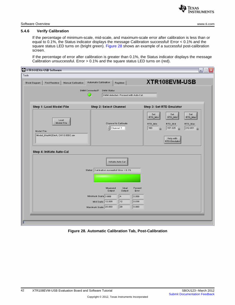
If the percentage of minimum-scale, mid-scale, and maximum-scale error after calibration is less than orequal to 0.1%, the Status indicator displays the message Calibration successful! Error < 0.1% and thesquare status LED turns on (bright green). Figure 28 shows an example of a successful post-calibrationscreen.
If the percentage of error after calibration is greater than 0.1%, the Status indicator displays the messageCalibration unsuccessful. Error > 0.1% and the square status LED turns on (red).
Figure 28. Automatic Calibration Tab, Post-Calibration
42 XTR108EVM-USB Evaluation Board and Software Tutorial SBOU123–March 2012Submit Documentation Feedback
Copyright © 2012, Texas Instruments Incorporated

www.ti.com Software Overview
5.5 Registers Tab
The Registers tab in the XTR108EVM-USB software enables the user to view and edit the contents ofeach register internal to the XTR108. Similar to the Block Diagram tab, it is recommended that onlyadvanced users make bit-level changes using this tab. However, for debugging purposes this capabilitycan be extremely useful.
Figure 29 shows the Registers tab. The actual values of each register may vary.
Figure 29. XTR108EVM-USB Software, Registers Tab
43SBOU123–March 2012 XTR108EVM-USB Evaluation Board and Software TutorialSubmit Documentation Feedback
Copyright © 2012, Texas Instruments Incorporated

Software Overview www.ti.com
5.5.1 Register and EEPROM Communications
The six buttons at the top of the Registers tab allow the user to perform read/write operations betweenthe XTR108EVM-USB software and the XTR108 registers and the EEPROM.
When clicked, The Read All Reg button reads the current XTR108 register values and loads them intosoftware, overwriting any current values. Similarly, the Write All Reg button writes the current softwareregister values to the actual registers within the XTR108.
The Read EEPROM button, when clicked, reads the current EEPROM values and loads them intosoftware, overwriting any current values. Similarly, the Write EEPROM button writes the current softwareregister values to the EEPROM.
If the XTR108EVM-USB software has made changes to the XTR108 register array within the software buthas not written those changes to the XTR108 registers, the Pending register changes need to be writtenLED turns on. Once the registers have been written, the LED turns off.
5.5.2 Save/Load Register Settings
The Save Register Settings button allows the user to save the current values of the register array as a.csv file. The default save location for register files is in the Register_files folder within the XTR108EVM-USB install directory (typically C:\Program Files\XTR108EVM-USB\). The Load Register Settings buttonallows the user to load a previously-saved register file, which can be useful for loading a set of calibratedregister values during production if calibration is not required for each board.
5.5.3 Register Table and Register Bits
Each register value is displayed in two forms: as a hexadecimal number within the Register Tableindicator, and as a sequence of binary bits in the Register Bits control. Clicking on the row of a registerwithin the Register Table indicator updates the contents of the Register Bits control to show the currently-selected register. Each bit is labeled in accordance with the register map given in the XTR108 data sheet.
If the selected register supports read/write operations, then each bit in the register can be set high or low('1' or '0', respectively) by using the arrow controls on the desired bit. Changes to the registers must bewritten using the Write All Reg button before taking effect.
Additional help for each register is available by selecting a register and clicking the Help with Registersbutton, which opens a help document specific to that register.
44 XTR108EVM-USB Evaluation Board and Software Tutorial SBOU123–March 2012Submit Documentation Feedback
Copyright © 2012, Texas Instruments Incorporated

www.ti.com Software Overview
5.6 Tools Menu
The Tools menu, located in the menu bar in the upper-left corner of the XTR108EVM-USB software,contains additional features useful for debugging or troubleshooting. The following sections explain theuse of each option within the Tools menu.
5.6.1 Control Bits
The Control Bits window, as shown in Figure 30, enables manual control of the signals that enable anddisable the XTR108EVM Interface Board relays. The control signals are off when the control is equal to '0'and are on when the control is equal to '1'. The functionality of each control bit is given by Table 27.
Figure 30. GPIO Control Window
Table 27. Control Bits Functions
BIT FUNCTION NOTES
Enables current When CTRL1 is enabled, the voltage measurement and resistance measurementCTRL1 measurement relay relays are disabled by circuit protection logic
Enables voltage When CTRL1 is enabled, the voltage measurement and resistance measurementCTRL2 measurement relay relays are disabled by circuit protection logic
Enables resistance When CTRL1 is enabled, the voltage measurement and resistance measurementCTRL3 measurement relay relays are disabled by circuit protection logic
Enables RTD_UNDER Enabling multiple RTD relays causes the resistances of each enabled RTD EmulatorCTRL4 relay channel to be connected in parallel
Enabling multiple RTD relays causes the resistances of each enabled RTD EmulatorCTRL5 Enables RTD_MIN relay channel to be connected in parallel
Enabling multiple RTD relays causes the resistances of each enabled RTD EmulatorCTRL6 Enables RTD_MID relay channel to be connected in parallel
Enabling multiple RTD relays causes the resistances of each enabled RTD EmulatorCTRL7 Enables RTD_MAX relay channel to be connected in parallel
Enabling multiple RTD relays causes the resistances of each enabled RTD EmulatorCTRL8 Enables RTD_OVER relay channel to be connected in parallel
45SBOU123–March 2012 XTR108EVM-USB Evaluation Board and Software TutorialSubmit Documentation Feedback
Copyright © 2012, Texas Instruments Incorporated

Software Overview www.ti.com
5.6.2 Debug Window
The Debug window, as shown in Figure 31, displays the input and output of all SPI communications. Thecommand lines follow the syntax of the tioScript mnemonic commands. More information on themnemonic commands is available in the Mnemonic Commands section.
Pressing the Clear button clears the strings displayed in the Debug Window until new communicationstake place.
Figure 31. Debug Window
5.6.3 About Window
The About window, as shown in Figure 32, lists the version, build date, and author of the currently-installed version of the XTR108EVM-USB software.
Figure 32. About Window
46 XTR108EVM-USB Evaluation Board and Software Tutorial SBOU123–March 2012Submit Documentation Feedback
Copyright © 2012, Texas Instruments Incorporated

VCC
JMP7CP SCK
NO CLK
SPI_SCKC11
R11C13
U3D2C12
R10
XTR108 IIN
330pF 30.1k36.5k
1nF
0.01PF
JMP6BYPASS
BUF
www.ti.com General Operating Tips
6 General Operating Tips
6.1 Voltage Output Mode
In many applications, it is desirable to bypass the FET and connect the XTR108 directly to the powersupply. This configuration can be completed by positioning jumpers JMP2 and JMP3 in the Bypassposition.
NOTE: You must be careful in this mode to not apply an overvoltage to the XTR108. The XTR108maximum supply voltage is 5.5 V. The voltage drop across D1 reduces the XTR108 supplyvoltage by approximately 0.7 V. To get an accurate idea of the XTR108 supply voltage whilein this mode, you should measure at the XTR108 VS pin.
6.2 Charge Pump
When the XTR108 is in voltage-output mode, a small negative voltage must be applied to the XTR108 IINpin to prevent the input offset voltage of the XTR108 current output stage from turning on the outputstage. A simple discrete charge pump circuit, shown in Figure 33, can be used to generate this smallnegative voltage. The charge pump input is the SPI clock to the XTR108.
Figure 33. Discrete Charge Pump on Sensor Interface Board
For this circuit to work, the XTR108 clock must toggle continuously. This toggling can be accomplished bykeeping the XTR108 in continuous EEPROM read mode. JMP6 can be used to connect or disconnect anexternal buffer to the XTR108 clock signal. More information regarding this charge pump is located in theXTR108 data sheet and the XTR108 Quick Start System Reference Guide.
47SBOU123–March 2012 XTR108EVM-USB Evaluation Board and Software TutorialSubmit Documentation Feedback
Copyright © 2012, Texas Instruments Incorporated

123456789
10111213141516171819202122232425
J6Male
ONE_WIRE
Vdut
Vcc
DAC_ADAC_BDAC_CDAC_D
ads2_Vin+
ads1_Vin+
ads2_Vin-
I2C_SDA_ISO
ads1_Vin-
I2C_SCK_ISO
INA-XTR -LoopXTR +Loop
-15V+15V
USB_DIO
USB_SCKUSB_CS1
I2C_SCKI2C_SDA2
123456789
10111213141516171819202122232425
J5Female
NCCTRL1CTRL2CTRL3CTRL4CTRL5CTRL6CTRL7CTRL8MEAS1MEAS2MEAS3MEAS4MEAS5MEAS6MEAS7MEAS8
CTRL1
RELAY_EN3
CTRL5
CTRL6
CTRL7
Relay1
VCC
Relay3
Relay5
Relay6
Relay7
POT2
POT1
R24N/I
R23N/I
R22N/I
POT4
POT3
R27N/I
R26N/I
R25N/I
POT6
POT5
R30N/I
R29N/I
R28N/I
12
3
JMP2
1
2
3
JMP3
1
2
3
JMP1
LO(F) LO(S) HI(F) HI(S)
Relay3
VCC
Relay3
VCC
VCC
RTD +
RTD +
VCC
RTD +
Relay5
VCC
RTD +
Relay6 Relay7
HI(F) LO(F)
Relay2
VCC
I(F)
LO(F)
HI(F)
LO(S)
HI(S)
LO(F) I(F)
VCC
Relay1
SCK DIOCS1
USB_SCK
USB_DIO
USB_CS1
123
J7
SPI
12
J2
12
J3
12
J4
Jumper
1-2 = POT Select2-3 = Resistor Seslect
Comments
JMP1JMP2JMP3
RTD -
RTD -
Panasonic Panasonic
1 2 3
J8 RTD_CON
RTD_MIN RTD_MID RTD_MAX
Vo_XTR108
Io_XTR108 Loop Supply
Io+
Io -
Vo +
Vo -
Rz
Rcm
Female
Io+
Io -
Vo +
Vo -
Rz_Out
Rcm
RTD +_Out
RTD Emulator (Min/Mid/Max)
RTD Sense -- 4-Wire RTD Measurement via DMM
SPI_SCK
SPI_DIO
SPI_CS1
SPI
Transmit Loop: Connect/Disconnect DMMVoltage Output Mode (Vout Measure)
Mode Comments
Relay 2 = ONVoltageMeasurement
Relay 1 = ON
Relay 3 = ON
Relay 4 = Under-scaleRelay 5 = MinRelay 6 = MidRelay 7 = MaxRelay 8 = Over-scale
CurrentMeasurement
RTDMeasurement
RTD Select
Relay Control
21
D0SMAJ6.0A
12
3
U4
BAT754S,215
R34
100
1HI(S)
1LO(S)
1HI(F)
1LO(F)
1I(F)
R31
100
R32
100
R35
100
R33
100
R36
100
12
3
U3
BAT754S,215
12
3
U2
BAT754S,215
VCCVCCVCC
Jumper Functionality
Relay Driver / Control Bits
R1010
3296Y-501
3296Y-1-100
500
10
3296Y-1-100 3296Y-1-100
10 10
500 500
R1110
R1210
3296Y-501 3296Y-501
RcmRz RTD
Vo -Vo +
Loop Supply +
Loop Supply -
Io +
Io -
R1
4.7k
R2
4.7k
R3
4.7k
R4
4.7k
R5
4.7k
R6
4.7k
R7
4.7k
CS1
SCK
DIO
POT_RTD R_RTD POT_RTD R_RTD POT_RTD R_RTD
C110uF
USB_DAQ_EVM_CONNECT
Rz
Rcm
RT
D
SPI_SCK
SPI_DIO
SPI_CS1
ON
192103114125136147158
J1
DB15
D5Relay 5
R14
510
D6Relay 6
Relay5 Relay6 Relay7
D7Relay 7
R16
510
R15
510
D4Relay 4
R13
510
D3
Relay 3
R20
510Relay3
Relay4
D1
Relay 1
R19
510Relay1
D2
Relay 2
R18
510Relay2
**Note: Relays Are Initially OFF. A CTRL Logic High Turns On Each Relay
**Note: SPI Data Input Connected to Data Output atPins 24, 25
Loop +
Loop -
Vo +
Vo -
Io +
Io -
XTR108 Sensor Board Connector
Multimeter Connect
Panasonic
ON
Panasonic
Vcc GND
VCC VCC VCC
VCC
VCC
VCC VCC
1 12
3
4
5
10
9
8
OFF
ONON
OFF
K5
TXS2SS-4.5V
1 12
3
4
5
10
9
8
OFF
ONON
OFF
K6
TXS2SS-4.5V
1 12
3
4
5
10
9
8
OFF
ONON
OFF
K7
TXS2SS-4.5V
1 12
3
4
5
10
9
8
OFF
ONON
OFF
K3_1
TXS2SS-4.5V
1 12
3
4
5
10
9
8
OFF
ONON
OFF
K3_2
TXS2SS-4.5V
1 12
3
4
5
10
9
8
OFF
ONON
OFF
K2
TXS2SS-4.5V
1 12
3
4
5
10
9
8
OFF
ONON
OFF
K1
TXS2SS-4.5V
12345678
TPG1
12345678
TPG2
CTRL1CTRL2CTRL3CTRL4CTRL5CTRL6CTRL7
Relay1Relay2Relay3Relay4Relay5Relay6Relay7
VCC
VCC
VCC
VCC
VCC
VCC
VCC
**Note: N/I = Not Installed
1
2
3
4
5 U6SN74AHC1G08DBVR
2
3
4
5 U5SN74AHC1G04DBVR
VCCVCC
Relay2
1
2
3
4
5 U7SN74AHC1G08DBVR
VCC
Relay4
CTRL1 CTRL2 CTRL3RELAY_EN2 RELAY_EN3
CTRL4
RELAY_EN2
Interface Protection: Relay 2/3 Enable
CTRL/Relay Test Connectors
C20.1uF
C30.1uF C4
0.1uF
GND1 GND2
CTRL8
Relay8
Rz_Out
RTD +_Out
1 12
3
4
5
10
9
8
OFF
ONON
OFF
K3_3
TXS2SS-4.5V
1 12
3
4
5
10
9
8
OFF
ONON
OFF
K4
TXS2SS-4.5V
1 12
3
4
5
10
9
8
OFF
ONON
OFF
K8
TXS2SS-4.5V
VCC
Rz_OutRTD +_Out
Relay3
RTD + Rz
**Note: K3 and K4 connect RTD emulator to DMM connectors. K8 disconnects RTD emulator from sensor board to ensure accurate readings when configuring pots.
VCC VCC
Relay4 Relay8
RTD + RTD +
D8Relay 8
R17
510Relay8
VCC
R910
R215k
RTD -
RTD Emulator (Under-scale/Over-scale)
Relay8CTRL8
R8
4.7k
VCC
1B1
2B2
3B3
4B4
5B5
6B6
7B7
8B8
GND9
1C18
2C17
3C16
4C15
5C14
6C13
8C11
COM10
7C12
U1 ULN2803A
Miscellaneous
Hardware Documentation www.ti.com
7 Hardware Documentation
This section provides the hardware documentation for the XTR108EVM-USB, including board schematics,layouts, and bill of materials.
7.1 Schematics
Figure 34 shows the XTR108EVM-USB Interface Board schematic.
Figure 34. XTR108EVM-USB Interface Board Schematic
48 XTR108EVM-USB Evaluation Board and Software Tutorial SBOU123–March 2012Submit Documentation Feedback
Copyright © 2012, Texas Instruments Incorporated

Q1
De
ple
tio
n M
od
e
RZ1
C2
RZ2
C3
RZ4
C5
RZ3
C4
RZ5
C6
RCM
Rlin15.8k
Rvi
R7 0
R8
0
R510k
V/I-1 V/I-0
V/I-4V/I-3 V/I-5
V/I-2
OPA_OUT
R9
0
REFout R_set
RSET
REFin
Io Vcc Vgate
F1
F2
D1
C8220pF
C92.2uF
C10
0.01uF
R_lin
Cfilter
Iin
Vo
OPA In +
VCC
VCC
SI5
SO2
HOLD7
WP3
Vcc
8V
ss
4
SCK6
CS1
U2
25C040
R11
30.1k
R1036.5k C13
330pF
C12
1nF
Charge Pump
24
53
U3
2
3
1
D2
VCC C110.01uF
C10.1uF
Iout
FET
CP
CP_ON
Vout
Bypass
Bypass
CP_OFF
VCC
GND GND GND GND GND GND
RL
R2 100
R3 100
R4 100
CS2
Load
Buf
Bypass
BBLOGO
TI LOGO
No Load
FET
123
J5
RTD_CON
1
2
3
JMP5
1
2
3 JMP4
12
3JMP6
1
2
3
JMP1
1
2
3
JMP7
1
2
3
JMP2
1
2
3
JMP3
12
J4
12
J3
Jumper Comments
1-2 = No Load (Voltage Mode)2-3 = Load (Current Mode)JMP4
1-2 = Current Mode2-3 = Use Charge Pump
Charge Pump (Voltage Mode):1-2 = Use Buffer2-3 = Bypass Buffer
1-2 = Current Mode2-3 = Voltage Mode
JMP5
JMP6
JMP3
JMP1
JMP2
JMP7
1-2 = Use FET2-3 = Bypass FET
1-2 = Use FET2-3 = Bypass FET
1-2 = No Charge Pump CLK2-3 = Charge Pump CLK = SPI_SCK
R149.9k
VCC
R6
Iout
Vo_XTR108
Io_XTR108
499
6.34k
12.1k
Steward HZ0603
Steward HZ0603
Io+
Io -
Vo +
Vo -
Rz
Rcm
RTD
Io+
Io -
Vo +
Vo -
Rz
Rcm
RTD
SPI_SCK
SPI_DIO
SPI_CS1
SPI_SCK
SPI_DIO
SPI_CS1
BAV99RWT1
1SS355TE-17
Male
SCK SDIO
OPA In -
Vo +
Vo -
CS1
RTDRzRcm
Io +
Io -
123
J1
SPI
SDIOSCKCS1
Note: 100V cap
V/I-01
V/I-12
V/I-23
V/I-34
V/I-45
V/I-56
Cfilte
r7
Rlin
8
Vo
9
Iin
10
Ire
t1
2
Io11
Vs13
Vgate14
REFin20
REFout21
Rset19
CS
21
5
CS
11
8
SC
LK
17
SD
IO1
6
OP
A+
In2
4
OP
A-I
n2
3
OPA OUT22
MUXPGA V/I
Voltage
Sub-Reg
SR and Control Circuits
Reference
DriverLinearization
U1
XTR108
SPI_SCK
CF
0.01uF
192
103
114
125
136
147
158
J2
DB15
C7
CAP
Rz
Rcm 1
2
3
JMP8
JMP81-2 = 2-Wire RTD2-3 = 3-Wire RTD
3-Wire RTD
2-Wire RTD
www.ti.com Hardware Documentation
Figure 35 shows the XTR108EVM-USB Sensor Board schematic.
Figure 35. XTR108EVM-USB Sensor Board Schematic
7.2 Layouts
Refer to Figure 15 for the XTR108EVM-USB Interface Board component-side layout. Refer to Figure 16for the XTR108EVM-USB Sensor Board component-side layout.
49SBOU123–March 2012 XTR108EVM-USB Evaluation Board and Software TutorialSubmit Documentation Feedback
Copyright © 2012, Texas Instruments Incorporated

Hardware Documentation www.ti.com
7.3 Bill of Materials (BOM)
Table 28 gives the XTR108EVM-USB Interface Board bill of materials. Table 29 gives the XTR108EVM-USB Sensor Board bill of materials.
Table 28. XTR108EVM-USB Interface Board Bill of Materials
Qty Value Ref Des Description Vendor Part Number
1 10µF C1 CAP CERAMIC 10UF 10V 0603 X5R ±20% TDK Corporation C1608X5R1A106M
3 0.1µF C2-C4 CAP .10UF 16V CERAMIC X7R 0603 Yageo CC0603KRX7R7BB104
8 4.7kΩ R1-R8 RES 4.70K OHM 1/10W 1% 0603 SMD ±100ppm/°C Panasonic - ECG ERJ-3EKF4701V
4 10Ω R9-R12 RES 10.0 OHM 1/10W 0.1% 0603 Vishay/Dale TNPW060310R0BEEA
8 510Ω R13-R20 RES 510 OHM 1/10W 1% 0603 SMD ±100ppm/°C Panasonic - ECG ERJ-3EKF5100V
1 4.99kΩ R21 RES 4.99K OHM 1/10W 1% 0603 SMD Panasonic - ECG ERJ-3EKF4991V
6 100Ω R31-R36 RES 100 OHM 1/10W 1% 0603 SMD ±100ppm/°C Panasonic - ECG ERJ-3EKF1000V
0 OMIT R22-R30 Omit; not installed N/A N/A
500Ω3 POT1, POT3, POT5 POT 500 OHM 3/8" SQ CERM SL MT Bourns Inc 3296Y-1-501LFPotentiometer
3 10Ω Potentiometer POT2, POT4, POT6 POT 10 OHM 3/8" SQ CERM SL MT Bourns Inc 3296Y-1-100LF
1 TVS Diode D0 TRANSIL 400W 6V UNIDIR SMA STMicroelectronics SMAJ6.0A-TR
8 LED (Red) D1-D8 LED RED HI BRT SS TYPE LO CUR SM Panasonic - SSG LNJ208R8ARA
LOW SIGNAL RELAYS - PCB 1A 4.5VDC DPDT10 TXS2SS-4.5V K1, K2, K3_1-K3_3, K4- K8 Panasonic Electric Works TXS2SS-4.5VNON-LATCHING SMD
1 ULN2803 U1 IC DUAL TRANS ARRAY HV 18-SOIC Texas Instruments ULN2803ADW
3 BAT754S U2-U4 DIODE SCHOTTKY 30V 200MA SOT-23 NXP Semiconductors BAT754S,215
1 SN74AHC1G04 U5 IC SINGLE INVERTER GATE SOT23-5 Texas Instruments SN74AHC1G04DBVR
2 SN74AHC1G08 U6, U7 IC SGL 2IN POS-AND GATE SOT23-5 Texas Instruments SN74AHC1G08DBVR
1 DSUB15F J1 CONN DB15 FEMAL .318" R/A NICKEL Norcomp Inc 182-015-213R531
3 2-pin Terminal J2-J4 TERMINAL BLOCK 5MM 2POS On Shore Technology Inc ED300/2
1 DSUB25M J5 CONN D-SUB RCPT R/A 25POS 30GOLD Tyco Electronics 5747846-4
1 DSUB25F J6 CONN D-SUB PLUG R/A 25POS 30GOLD Tyco Electronics 5747842-4
2 3-pin Terminal J7, J8 TERMINAL BLOCK 5MM 3POS On Shore Technology Inc ED300/3
2 8-position Header TPG1, TPG2 CONN HEADER 8POS .100" SGL GOLD Samtec TSW-108-07-G-S
GND, GND1, GND2, Rz, RTD, Io+, Io–, Loop Supply+, Loop17 TP Cut to Size CONN. HEADER .100 SNGL 1POS Samtec TSW-101-07-G-SSupply–, Vo+, Vo–, CS1, SCK, DIO, Rcm, GND, Vcc
3 3-position Jumper JMP1-JMP3 CONN HEADER .100 SNGL 3POS Samtec TSW-103-07-G-S
3 Jumper Shunts JMP1-JMP3 JUMPER SHORTING UNITS Tyco Electronics 881545-2
BANANA AND BINDING POST CONNECTORS3 Banana Plug (Red) I(F), HI(S), HI(F) Emerson/Johnson 111-0702-001BINDING POST RED
Banana Plug BANANA AND BINDING POST CONNECTORS2 LO(S), LO(F) Emerson/Johnson 111-0703-001(Black) BINDING POST BLACK
4 Screws N/A SCREW MACHINE PHILLIPS 4-40X3/8 B&F Fastener Supply PMS 440 0038 PH
4 Standoffs N/A STANDOFF HEX 4-40THR ALUM .500"L Keystone Electronics 2203
50 XTR108EVM-USB Evaluation Board and Software Tutorial SBOU123–March 2012Submit Documentation Feedback
Copyright © 2012, Texas Instruments Incorporated

www.ti.com Hardware Documentation
Table 29. XTR108EVM-USB Sensor Board Bill of Materials
Qty Value Ref Des Description Vendor Part Number
1 0.1µF C1 CAP CER .10UF 25V X7R 10% 0603 TDK Corporation C1608X7R1E104K
1 220pF C8 CAP CER 220PF 50V X7R 10% 0603 TDK Corporation C1608X7R1H221K
1 2.2µF C9 CAP CER 2.2UF 16V Y5V 0603 TDK Corporation C1608Y5V1C225Z
3 10000pF C10, C11, CF CAP CER 10000PF 100V X7R 10% 0603 TDK Corporation C1608X7R2A103K
1 1000pF C12 CAP CER 1000PF 50V 10% X7R 0603 Murata Electronics GRM188R71H102KA01D
1 330pF C13 CAP CERAMIC 330PF 50V NP0 0603 Yageo CC0603JRNP09BN331
1 49.9kΩ R1 RES 49.9K OHM 1/10W 1% 0603 SMD Panasonic - ECG ERJ-3EKF4992V
3 100Ω R2-R4 RES 100 OHM 1/10W 1% 0603 SMD Panasonic - ECG ERJ-3EKF1000V
1 10kΩ R5 RES 10.0K OHM 1/10W 1% 0603 SMD Panasonic - ECG ERJ-3EKF1002V
3 0Ω R7-R9 RES 0.0 OHM 1/10W 5% 0603 SMD Yageo RC0603JR-070RL
1 36.5kΩ R10 RES 36.5K OHM 1/10W 1% 0603 SMD Panasonic - ECG ERJ-3EKF3652V
1 30.1kΩ R11 RES 30.1K OHM 1/10W 1% 0603 SMD Panasonic - ECG ERJ-3EFK3012V
1 549Ω RCM RES 549 OHM 1/10W 1% 0603 SMD Panasonic - ECG ERJ-3EKF5490V
1 34kΩ RLIN RES 34K OHM 1/16W .5% 0603 SMD Susumu Co Ltd RR0816P-3402-D-52C
1 12.1kΩ RSET RES 12.1K OHM 1/16W .5% 0603 SMD Susumu Co Ltd RR0816P-1212-D-09C
1 6.34kΩ RVI RES 6.34K OHM 1/16W .5% 0603 SMD Susumu Co Ltd RR0816P-6341-D-78H
1 100.0Ω RZ1 RES 100 OHM 1/10W .1% 0603 SMD Panasonic - ECG ERA-3AEB101V
0 OMIT RZ2-RZ5, RL, R6, C2-C7 Omit; not installed N/A N/A
1 1SS355TE-17 D1 DIODE SWITCH 90V 100MA SOT-323 Rohm Semiconductor 1SS355TE-17
1 BAV99 D2 DIODE SWITCH SS DUAL 70V SOT323 ON Semiconductor BAV99RWT1G
2 Ferrite F1, F2 FERRITE 300MA 600 OHM 0603 SMD Laird-Signal Integrity Products HZ0603C601R-10
1 NFET Q1 MOSFET, N CHANNEL, DEPLETION MODE Supertex DN2540N8
1 XTR108 U1 IC 4-20MA 2-WIRE TRNSMTR 24-QSOP Texas Instruments XTR108EA
1 25C040/SN U2 IC EEPROM 4KBIT 3MHZ 8SOIC Microchip Technology 25C040/SN
1 SN74LVC1G04 U3 IC SINGLE INVERTER-GATE SC-70 Texas Instruments SN74LVC1G04DCKT
9 Pin Socket RZ1-RZ5, RCM, RLIN, RSET CONN SOCKET RCPT .014-.026 30AU Tyco Electronics 5050863-5
2 3-pin Terminal J1, J5 TERMINAL BLOCK 5MM 3POS On Shore Technology Inc ED300/3
1 DSUB15M J2 CONN DB15 MALE .318" R/A NICKEL Norcomp Inc 182-015-113R531
2 2-pin Terminal J3, J4 TERMINAL BLOCK 5MM 2POS On Shore Technology Inc ED300/2
REFout, REFin, R_set, SCK, CS1, CS2, SDIO, Vcc, Io, Vgate,29 TP Cut to Size GND1-GND6, Iin, Vo, V/I-0 to V/I-5, R_lin, Cfilter, OPA In+, CONN. HEADER .100 SNGL 1POS Samtec TSW-101-07-G-S
OPA In–, OPAout
HEADER, 3 POSITION, SINGLE ROW, GOLD,8 3-position Jumper JMP1-JMP8 Samtec TSW-103-07-G-S0.100"
8 Jumper Shunts JMP1-JMP8 JUMPER SHORTING UNITS Tyco Electronics 881545-2
4 Screws N/A SCREW MACHINE PHILLIPS 4-40X3/8 B&F Fastener Supply PMS 440 0038 PH
4 Standoffs N/A STANDOFF HEX 4-40THR ALUM .500"L Keystone Electronics 2203
51SBOU123–March 2012 XTR108EVM-USB Evaluation Board and Software TutorialSubmit Documentation Feedback
Copyright © 2012, Texas Instruments Incorporated
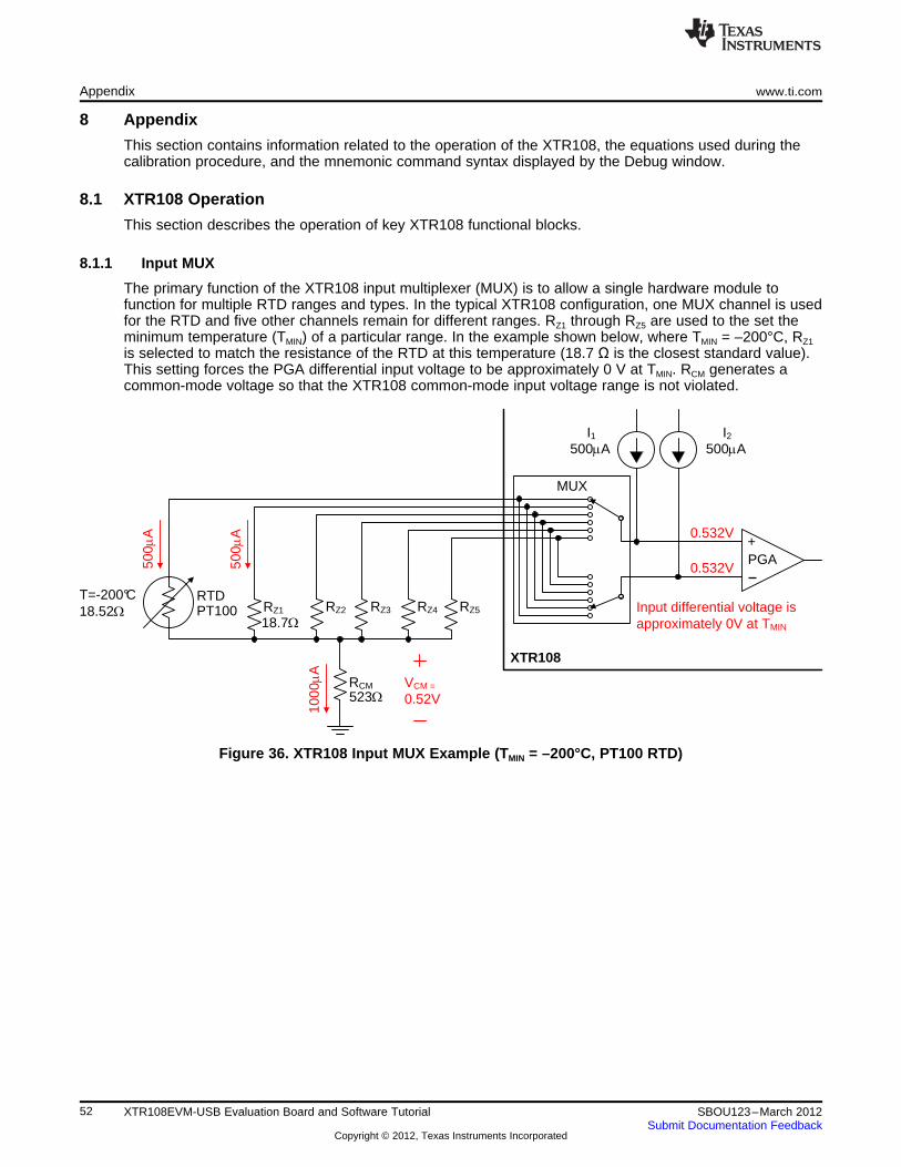
RCM523:
RZ2 RZ3 RZ4 RZ5RZ1
18.7:
RTDPT100
+PGA
XTR108
T=-200°C18.52:
500PA 500PAI1 I2
VCM =
0.52V
0.532V
0.532V
1000P
A
500P
A
500P
A
Input differential voltage is approximately 0V at TMIN
MUX
Appendix www.ti.com
8 Appendix
This section contains information related to the operation of the XTR108, the equations used during thecalibration procedure, and the mnemonic command syntax displayed by the Debug window.
8.1 XTR108 Operation
This section describes the operation of key XTR108 functional blocks.
8.1.1 Input MUX
The primary function of the XTR108 input multiplexer (MUX) is to allow a single hardware module tofunction for multiple RTD ranges and types. In the typical XTR108 configuration, one MUX channel is usedfor the RTD and five other channels remain for different ranges. RZ1 through RZ5 are used to the set theminimum temperature (TMIN) of a particular range. In the example shown below, where TMIN = –200°C, RZ1
is selected to match the resistance of the RTD at this temperature (18.7 Ω is the closest standard value).This setting forces the PGA differential input voltage to be approximately 0 V at TMIN. RCM generates acommon-mode voltage so that the XTR108 common-mode input voltage range is not violated.
Figure 36. XTR108 Input MUX Example (TMIN = –200°C, PT100 RTD)
52 XTR108EVM-USB Evaluation Board and Software Tutorial SBOU123–March 2012Submit Documentation Feedback
Copyright © 2012, Texas Instruments Incorporated

RCM523:
RZ2 RZ3 RZ4 RZ5RZ1
18.7:
RTDPT100
+PGA
XTR108
T=850°C390.48:
500PA 500PAI1 I2
VCM =
0.52V
0.718V
0.532V10
00P
A
500P
A
500P
A
Input differential voltage is approximately 186mV at TMAX
MUX
RCM5.23k:
RZ2 RZ3 RZ4 RZ5RZ1
187:
RTDPT1000
+PGA
XTR108
T=850°C3.905k:
50PA 50PAI1 I2
VCM =
0.52V
0.718V
0.532V
100P
A
50P
A
50P
A
Input differential voltage is approximately 186mV at TMAX
MUX
www.ti.com Appendix
Figure 37 shows the same multiplexer configuration with the RTD at maximum temperature, where TMAX =+850°C. At this point, the differential input voltage to the PGA is equal to 186 mV, the maximum value forthis configuration.
Figure 37. XTR108 Input MUX Example (TMAX = +850°C, PT100 RTD)
Figure 38 shows how the current sources can be programmed to accommodate different types of RTDs.The previous example used a 100-Ω RTD, or PT100. In this example the RTD type has been changed to1000 Ω, or PT1000. The current sources I1 and I2 are scaled from 500 µA to 50 µA to accommodate thisnew resistance. RZ1 and RCM are also scaled appropriately. Note that I1 and I2 are matched current sourcesthat are programmed by one set of DACs (an 8-bit coarse DAC and 8-bit fine DAC). These currentsources are programmed during the calibration procedure.
Figure 38. XTR108 Input MUX Example (TMAX = +850°C, PT1000 RTD)
53SBOU123–March 2012 XTR108EVM-USB Evaluation Board and Software TutorialSubmit Documentation Feedback
Copyright © 2012, Texas Instruments Incorporated

RCM
RZ2 RZ3 RZ4 RZ5RZ1
+PGA
XTR108
Mul
tiple
xer
V/I-5V/I-4
V/I-3
V/I-2V/I-1
V/I-0
I1 I2
LinearizationCircuit
ZeroDAC
ILIN
DAC
IREF
DAC
CFILT RLIN
RTD
RSET
0.01PF 34.0k: 12.1k:
RCM
RZ2 RZ3 RZ4 RZ5RZ1
+PGA
XTR108
Mul
tiple
xer
V/I-5V/I-4
V/I-3
V/I-2V/I-1
V/I-0
I1 I2
LinearizationCircuit
ZeroDAC
ILIN
DAC
IREF
DAC
CFILT RLIN
RTD
RSET
0.01PF 34.0k: 12.1k:
Appendix www.ti.com
8.1.2 RSET
The range of the IREF DAC that controls the current sources I1 and I2 is set by the external resistor RSET.For example, with a value of RSET = 12.1 kΩ, the range of IREF is 480 µA to 510 µA. If RSET = 121 kΩ, therange of IREF becomes 48 µA to 51 µA. The Find Resistors tab within the XTR108EVM-USB softwarehelps to determine the appropriate RSET value.
Figure 39. RSET Circuitry
8.1.3 RLIN
All RTDs have a nonlinear response over temperature. Typically, this nonlinearity can be approximated asa second-order function, and therefore can be calibrated out by modulating the excitation current with theRTD input signal. The range of this linearity correction is set by external resistor, RLIN.
Figure 40. RLIN Circuitry
54 XTR108EVM-USB Evaluation Board and Software Tutorial SBOU123–March 2012Submit Documentation Feedback
Copyright © 2012, Texas Instruments Incorporated

50
100
150
200
250
300
350
−200 0 200 400 600 800Temperature (°C)
Res
ista
nce
(Ω)
RTD ResponseCorrected ResponseLinearization Correction
G000
−1
0
1
2
3
4
5
−200 0 200 400 600 800Temperature (°C)
Non
linea
rity
(%)
UncorrectedCorrected
G000
www.ti.com Appendix
8.1.4 Linearity Correction
Figure 41 illustrates how the XTR108 linearity correction works. The RTD has a response that isapproximately quadratic (gray line). The positive feedback of the input signal through the linearity DAC ILIN
generates a response that is also approximately quadratic (black line). The two responses counteracteach other to generate a linear output (red line).
Figure 41. Linearity Correction Method
Figure 42 shows the uncorrected and corrected nonlinearity for a typical RTD. Normally a 40:1improvement is achieved using this method.
Figure 42. Linearity Improvement
55SBOU123–March 2012 XTR108EVM-USB Evaluation Board and Software TutorialSubmit Documentation Feedback
Copyright © 2012, Texas Instruments Incorporated

BV = RTDMAX - RTDMIN
RTDMID - 2RTDMAX + RTDMIN
GLIN = (0.5 + BV)*RTDMAX - (0.5 - BV)*RTDMIN - 2*BV*RZ
2*BV
GLIN_MAX = RLIN
16
ISET =
50*APGA*(RTDMAX - RTDMIN)(IOUT_MAX - IOUT_MIN)*[1 - GLIN*(RTDMAX - RZ)]*RVI
VREF = 1.193V
IREF =
RSET
VREF
IREF_MIN = 0.65*(5*ISET)
IREF_MAX = 1.35*(5*ISET)
Appendix www.ti.com
8.2 XTR108 Calibration Equations (Current-Output Mode)
The following section gives the equations used during the calibration procedure for current-output mode.
8.2.1 Initial Calculations
8.2.1.1 RTD Resistance
The equations in Table 30 are used to calculate the RTD resistance at the minimum temperature(RTDMIN), medium temperature (RTDMID), and maximum temperature (RTDMAX). Pick an external zeroresistor, RZ, that is the closest standard value to RTDMIN.
Table 30. Standard RTD Equations (1)
If –200°C < T < 0°C If T > 0°C
Rt = R0 [1 + A × T + B × T2 + C × T3(T – 100°C)] Rt = R0 [1 + A × T + B × T2](1) A = 3.9083E-3, B = –5.775E-7, C = –4.183E-12, R0 = RTD value at 0°C (typically 100 Ω or 1 kΩ), and T = temperature in °C.
8.2.1.2 Relative Nonlinearity
Calculate the relative nonlinearity, BV, by using the RTD values calculated in the previous step.
8.2.1.3 Linearization Coefficient
Calculate the linearization coefficient, GLIN.
Calculate GLIN_MAX. If GLIN is larger than GLIN_MAX, the external resistor RLIN must be changed.
8.2.1.4 IREF DAC (Excitation Current Source)
Choose the minimum and maximum output current values (IOUT_MIN and IOUT_MAX). Select an initial PGA gainsetting (APGA) and calculate the initial excitation current IREF. Ensure that the PGA gain is selected suchthat IREF_MIN < IREF < IREF_MAX.
56 XTR108EVM-USB Evaluation Board and Software Tutorial SBOU123–March 2012Submit Documentation Feedback
Copyright © 2012, Texas Instruments Incorporated

50*APGA*IREF*(RTDMIN - RZ)RVI
IZERO = IOUT_MIN -
5*VREF
8*RVIIZPGM =
IREF - 5*ISET - N10 = round[1024 * ]ISET
N11*ISET
64
IREF - 5*ISET
N11 = round[64 * ]ISET
N13 = round[4 * ]IZPGM
IZERO - 35*IZPGM
N12 = round[64 * ]IZPGM
N13*IZPGM
4IZERO - 35*IZPGM -
(IOUT_MAX_MEAS - IOUT_MIN_MEAS)*RVI
50*APGA*(RTDMAX - RTDMIN)IREF_A =
(IZERO - IOUT_MIN_MEAS)*RVI
50*APGA*IREF_AdRZ =
RZ_A = RTDMIN + dRZ
2*BV
(0.5 + BV)*RTDMAX - (0.5 - BV)*RTDMIN - 2*BV*RZ_AGLIN_A =
N14 = round(16*GLIN_A*RLIN)
www.ti.com Appendix
8.2.1.5 IZERO DAC (Zero Offset)
Calculate the required IZERO DAC value.
8.2.1.6 Calculate DAC Codes
The IREF and IZERO DACs are controlled by registers 10, 11, 12, and 13 in the XTR108. Use the followingequations to determine the values to be written to these registers. N10, N11, N12, and N13 are decimalvalues that must be converted to hexadecimal before being written.
8.2.2 First Corrections
First, measure the output current at the minimum and maximum temperatures (IOUT_MIN_MEAS andIOUT_MAX_MEAS).
8.2.2.1 Linearization Register
Calculate the corrections for the linearization register. N14 is a decimal value that must be converted tohexadecimal before being written.
57SBOU123–March 2012 XTR108EVM-USB Evaluation Board and Software TutorialSubmit Documentation Feedback
Copyright © 2012, Texas Instruments Incorporated

N11
64IREF_REG = ISET*[5 + + ]dIREF = (IREF_REG ± IREF_A) + (IREF_REG - IREF_B)
N10_A = N10 + round[ ]N11_A = N11
(IOUT_MAX - IOUT_MIN)*[1 - GLIN_A*(RTDMAX - RZ_A)]*RVI
50*APGA*(RTDMAX ± RTDMIN)IREF_B =
N10
1024
1024*dIREF*RSET
VREF
N11_A = round[64* ]
N10_A = round[1024* ]
IREF_ADJ = IREF_REG + dIREF
IREF_ADJ - 5*ISET
ISET
IREF_ADJ - 5*ISET - ISET
N11_A*ISET
64
N12_A = round[N12 + ]N13_A = N13
dIZERO = IOUT_MIN - IZERO - [ ]512*dIZERO - 35*IZPGM
IZPGM
50*APGA*IREF_B*(RTDMIN ± RZ_A)RVI
N13_A = round[4* ]
N12_A = round[64* ]
IZERO + dIZERO - 35*IZPGM
IZPGM
IZERO + dIZERO - 35*IZPGM - IZPGM
IZPGM*N13_A
4
Appendix www.ti.com
8.2.2.2 IREF Registers
Calculate the corrections for the IREF registers.
NOTE: If the adjusted value for register 10 (N10_A) is outside of the possible range of –127 < N10_A <128, then use the following equations to adjust both register 10 and register 11.
8.2.2.3 IZERO Registers
Calculate the corrections for the IZERO registers.
NOTE: If the adjusted value for register 12 (N12_A) is outside of the possible range of –127 < N12_A <128, then use the following equations to adjust both register 12 and register 13.
58 XTR108EVM-USB Evaluation Board and Software Tutorial SBOU123–March 2012Submit Documentation Feedback
Copyright © 2012, Texas Instruments Incorporated

ILIN_A = IREF_B*APGA*50*(RTDMAX-RTDMIN)
RVI
ILIN_B = IOUT_MAX_MEAS_2 ± IOUT_MIN
GLIN_MEAS_A = ILIN_B ± ILIN_A
(RTDMAX-RZ_A)*ILIN_B
GLIN_FINAL = GLIN_A* GLIN_A
GLIN_MEAS_A
N14_A = round(16*GLIN_FINAL*RLIN)
IOUT = VOUT*50
RVI
www.ti.com Appendix
8.2.3 Second Corrections
Measure the output current at the maximum temperature (IOUT_MAX_MEAS_2).
8.2.3.1 Linearization Register
Calculate the final corrections for the linearization register. This step completes the calibration procedure.
8.3 XTR108 Calibration Equations (Voltage-Output Mode)
The calibration procedure for voltage-output mode is exactly the same as for current-output mode. Theonly difference is that output voltage must be converted to output current in order to satisfy the same setsof equations. Use the following equation to convert output voltage to output current.
8.4 Mnemonic Commands
The USB-DAQ platform uses a set of mnemonic commands to perform SPI communications to theXTR108EVM-USB. These commands are given in Table 31.
Table 31. Mnemonic Commands
Command Description
SPI Always the first mnemonic in an SPI command.
Always the second mnemonic in an SPI command.CH1 This mnemonic identifies which SPI channel is used. The USB-DAQ platform containsCH2 two SPI channels to allow for the connection of two different SPI devices.
BREH Always the third mnemonic in an SPI command.BREL This mnemonic identifies different modes of SPI data capture. For example, BRELAFEH means that the data are captured before the clock rising edge and the clock is activeAFEL low. Further details are included in Table 32.
L Drive chip select (CS) line low
H Drive chip select (CS) line high
R Read an 8-bit word
Example: 01h, 3Ah, and 9Ch Write an 8-bit word (any hexadecimal two-character byte)
59SBOU123–March 2012 XTR108EVM-USB Evaluation Board and Software TutorialSubmit Documentation Feedback
Copyright © 2012, Texas Instruments Incorporated

Appendix www.ti.com
The USB-DAQ Platform SPI protocol supports four clock and data line modes of operation. These modesare summarized in Table 32. The first mode, BREH, is used by the XTR108EVM-USB.
Table 32. SPI Modes of Operation
Mode Clock Polarity Description (CPOL) Clock Transition for Data Polarity Description (CPHA)
Data are read by the USB-DAQ on the clock rising edge. Data areClock idles lowBREH changed by the USB-DAQ on the clock falling edge. Data are sampled onCPOL = 0 the first clock edge. CPHA = 0.
Data are read by the USB-DAQ on the clock falling edge. Data areClock idles lowBREL changed by the USB-DAQ on the clock rising edge. Data are sampled onCPOL = 0 the second clock edge. CPHA = 1.
Data are read by the USB-DAQ on the clock falling edge. Data areClock idles highAFEH changed by the USB-DAQ on the clock rising edge. Data are sampled onCPOL = 1 the first clock edge. CPHA = 0.
Data are read by the USB-DAQ on the clock rising edge. Data areClock idles highAFEL changed by the USB-DAQ on the clock falling edge. Data are sampled onCPOL = 1 the second clock edge. CPHA = 1.
The USB-DAQ also supports a set of generic commands used to enable or disable power supplies, readfrom internal ADCs, set the output of internal DACs, and set the voltage of control pins. The XTR108EVM-USB uses the GPIO pin functionality to control the relay driver U1 on the Interface Board. Thesecommands are given in Table 33.
Table 33. General USB-DAQ Commands
Command Description
CMD Always the first mnemonic in a general USB-DAQ command.
Sets the eight control pins according to the value written.Each control pin is assigned a location in the 8-bit control word, where CTRL8 is theExample: CTRL 0, CTRL 3, CTRL 128, MSB and CTRL1 is the LSB. For example, write CTRL 0 to turn off all control pins. ToCTRL 255 turn on the CTRL1 and CTRL2 pins, write CTRL 3. To turn on only the CTRL8 pin,write CTRL 128.
60 XTR108EVM-USB Evaluation Board and Software Tutorial SBOU123–March 2012Submit Documentation Feedback
Copyright © 2012, Texas Instruments Incorporated

FCC Warning
This evaluation board/kit is intended for use for ENGINEERING DEVELOPMENT, DEMONSTRATION, OR EVALUATION PURPOSESONLY and is not considered by TI to be a finished end-product fit for general customer use. It generates, uses, and can radiate radiofrequency energy and has not been tested for compliance with the limits of computing devices pursuant to part 15 of FCC rules, which aredesigned to provide reasonable protection against radio frequency interference. Operation of this equipment in other environments maycause interference with radio communications, in which case the user at his own expense will be required to take whatever measures maybe required to correct this interference.
EVALUATION BOARD/KIT IMPORTANT NOTICE
Texas Instruments (TI) provides the enclosed product(s) under the following conditions:
This evaluation board/kit is intended for use for ENGINEERING DEVELOPMENT, DEMONSTRATION, OR EVALUATION PURPOSESONLY and is not considered by TI to be a finished end-product fit for general consumer use. Persons handling the product(s) must haveelectronics training and observe good engineering practice standards. As such, the goods being provided are not intended to be completein terms of required design-, marketing-, and/or manufacturing-related protective considerations, including product safety and environmentalmeasures typically found in end products that incorporate such semiconductor components or circuit boards. This evaluation board/kit doesnot fall within the scope of the European Union directives regarding electromagnetic compatibility, restricted substances (RoHS), recycling(WEEE), FCC, CE or UL, and therefore may not meet the technical requirements of these directives or other related directives.
Should this evaluation board/kit not meet the specifications indicated in the User’s Guide, the board/kit may be returned within 30 days fromthe date of delivery for a full refund. THE FOREGOING WARRANTY IS THE EXCLUSIVE WARRANTY MADE BY SELLER TO BUYERAND IS IN LIEU OF ALL OTHER WARRANTIES, EXPRESSED, IMPLIED, OR STATUTORY, INCLUDING ANY WARRANTY OFMERCHANTABILITY OR FITNESS FOR ANY PARTICULAR PURPOSE.
The user assumes all responsibility and liability for proper and safe handling of the goods. Further, the user indemnifies TI from all claimsarising from the handling or use of the goods. Due to the open construction of the product, it is the user’s responsibility to take any and allappropriate precautions with regard to electrostatic discharge.
EXCEPT TO THE EXTENT OF THE INDEMNITY SET FORTH ABOVE, NEITHER PARTY SHALL BE LIABLE TO THE OTHER FOR ANYINDIRECT, SPECIAL, INCIDENTAL, OR CONSEQUENTIAL DAMAGES.
TI currently deals with a variety of customers for products, and therefore our arrangement with the user is not exclusive.
TI assumes no liability for applications assistance, customer product design, software performance, or infringement of patents orservices described herein.
Please read the User’s Guide and, specifically, the Warnings and Restrictions notice in the User’s Guide prior to handling the product. Thisnotice contains important safety information about temperatures and voltages. For additional information on TI’s environmental and/orsafety programs, please contact the TI application engineer or visit www.ti.com/esh.
No license is granted under any patent right or other intellectual property right of TI covering or relating to any machine, process, orcombination in which such TI products or services might be or are used.
EVM WARNINGS AND RESTRICTIONS
The loop supply (J4 on Interface Board, J3 on Sensor Board) input voltage range is (3.0V to 5.5V) + VD1 when in Voltage-output mode.When operating in Current-output mode, the loop supply input voltage range is 12V to 24V. In general, you must consider the powerdissipated in the external transistor and the operating temperature of the transistor in order to determine the maximum loop voltage andcurrent. This calculation is determined in the XTR108 data sheet.
Exceeding the specified input range may cause unexpected operation and/or irreversible damage to the EVM. If there are questionsconcerning the input range, please contact a TI field representative prior to connecting the input power.
Applying loads outside of the specified output range may result in unintended operation and/or possible permanent damage to the EVM.Please consult the EVM User's Guide prior to connecting any load to the EVM output. If there is uncertainty as to the load specification,please contact a TI field representative.
Mailing Address: Texas Instruments, Post Office Box 655303, Dallas, Texas 75265Copyright © 2005, Texas Instruments Incorporated

EVALUATION BOARD/KIT/MODULE (EVM) ADDITIONAL TERMSTexas Instruments (TI) provides the enclosed Evaluation Board/Kit/Module (EVM) under the following conditions:
The user assumes all responsibility and liability for proper and safe handling of the goods. Further, the user indemnifies TI from all claimsarising from the handling or use of the goods.
Should this evaluation board/kit not meet the specifications indicated in the User’s Guide, the board/kit may be returned within 30 days fromthe date of delivery for a full refund. THE FOREGOING LIMITED WARRANTY IS THE EXCLUSIVE WARRANTY MADE BY SELLER TOBUYER AND IS IN LIEU OF ALL OTHER WARRANTIES, EXPRESSED, IMPLIED, OR STATUTORY, INCLUDING ANY WARRANTY OFMERCHANTABILITY OR FITNESS FOR ANY PARTICULAR PURPOSE. EXCEPT TO THE EXTENT OF THE INDEMNITY SET FORTHABOVE, NEITHER PARTY SHALL BE LIABLE TO THE OTHER FOR ANY INDIRECT, SPECIAL, INCIDENTAL, OR CONSEQUENTIALDAMAGES.
Please read the User's Guide and, specifically, the Warnings and Restrictions notice in the User's Guide prior to handling the product. Thisnotice contains important safety information about temperatures and voltages. For additional information on TI's environmental and/or safetyprograms, please visit www.ti.com/esh or contact TI.
No license is granted under any patent right or other intellectual property right of TI covering or relating to any machine, process, orcombination in which such TI products or services might be or are used. TI currently deals with a variety of customers for products, andtherefore our arrangement with the user is not exclusive. TI assumes no liability for applications assistance, customer product design,software performance, or infringement of patents or services described herein.
REGULATORY COMPLIANCE INFORMATIONAs noted in the EVM User’s Guide and/or EVM itself, this EVM and/or accompanying hardware may or may not be subject to the FederalCommunications Commission (FCC) and Industry Canada (IC) rules.
For EVMs not subject to the above rules, this evaluation board/kit/module is intended for use for ENGINEERING DEVELOPMENT,DEMONSTRATION OR EVALUATION PURPOSES ONLY and is not considered by TI to be a finished end product fit for general consumeruse. It generates, uses, and can radiate radio frequency energy and has not been tested for compliance with the limits of computingdevices pursuant to part 15 of FCC or ICES-003 rules, which are designed to provide reasonable protection against radio frequencyinterference. Operation of the equipment may cause interference with radio communications, in which case the user at his own expense willbe required to take whatever measures may be required to correct this interference.
General Statement for EVMs including a radioUser Power/Frequency Use Obligations: This radio is intended for development/professional use only in legally allocated frequency andpower limits. Any use of radio frequencies and/or power availability of this EVM and its development application(s) must comply with locallaws governing radio spectrum allocation and power limits for this evaluation module. It is the user’s sole responsibility to only operate thisradio in legally acceptable frequency space and within legally mandated power limitations. Any exceptions to this are strictly prohibited andunauthorized by Texas Instruments unless user has obtained appropriate experimental/development licenses from local regulatoryauthorities, which is responsibility of user including its acceptable authorization.
For EVMs annotated as FCC – FEDERAL COMMUNICATIONS COMMISSION Part 15 Compliant
CautionThis device complies with part 15 of the FCC Rules. Operation is subject to the following two conditions: (1) This device may not causeharmful interference, and (2) this device must accept any interference received, including interference that may cause undesired operation.
Changes or modifications not expressly approved by the party responsible for compliance could void the user's authority to operate theequipment.
FCC Interference Statement for Class A EVM devicesThis equipment has been tested and found to comply with the limits for a Class A digital device, pursuant to part 15 of the FCC Rules.These limits are designed to provide reasonable protection against harmful interference when the equipment is operated in a commercialenvironment. This equipment generates, uses, and can radiate radio frequency energy and, if not installed and used in accordance with theinstruction manual, may cause harmful interference to radio communications. Operation of this equipment in a residential area is likely tocause harmful interference in which case the user will be required to correct the interference at his own expense.

FCC Interference Statement for Class B EVM devicesThis equipment has been tested and found to comply with the limits for a Class B digital device, pursuant to part 15 of the FCC Rules.These limits are designed to provide reasonable protection against harmful interference in a residential installation. This equipmentgenerates, uses and can radiate radio frequency energy and, if not installed and used in accordance with the instructions, may causeharmful interference to radio communications. However, there is no guarantee that interference will not occur in a particular installation. Ifthis equipment does cause harmful interference to radio or television reception, which can be determined by turning the equipment off andon, the user is encouraged to try to correct the interference by one or more of the following measures:
• Reorient or relocate the receiving antenna.• Increase the separation between the equipment and receiver.• Connect the equipment into an outlet on a circuit different from that to which the receiver is connected.• Consult the dealer or an experienced radio/TV technician for help.
For EVMs annotated as IC – INDUSTRY CANADA Compliant
This Class A or B digital apparatus complies with Canadian ICES-003.
Changes or modifications not expressly approved by the party responsible for compliance could void the user’s authority to operate theequipment.
Concerning EVMs including radio transmitters
This device complies with Industry Canada licence-exempt RSS standard(s). Operation is subject to the following two conditions: (1) thisdevice may not cause interference, and (2) this device must accept any interference, including interference that may cause undesiredoperation of the device.
Concerning EVMs including detachable antennasUnder Industry Canada regulations, this radio transmitter may only operate using an antenna of a type and maximum (or lesser) gainapproved for the transmitter by Industry Canada. To reduce potential radio interference to other users, the antenna type and its gain shouldbe so chosen that the equivalent isotropically radiated power (e.i.r.p.) is not more than that necessary for successful communication.
This radio transmitter has been approved by Industry Canada to operate with the antenna types listed in the user guide with the maximumpermissible gain and required antenna impedance for each antenna type indicated. Antenna types not included in this list, having a gaingreater than the maximum gain indicated for that type, are strictly prohibited for use with this device.
Cet appareil numérique de la classe A ou B est conforme à la norme NMB-003 du Canada.
Les changements ou les modifications pas expressément approuvés par la partie responsable de la conformité ont pu vider l’autorité del'utilisateur pour actionner l'équipement.
Concernant les EVMs avec appareils radio
Le présent appareil est conforme aux CNR d'Industrie Canada applicables aux appareils radio exempts de licence. L'exploitation estautorisée aux deux conditions suivantes : (1) l'appareil ne doit pas produire de brouillage, et (2) l'utilisateur de l'appareil doit accepter toutbrouillage radioélectrique subi, même si le brouillage est susceptible d'en compromettre le fonctionnement.
Concernant les EVMs avec antennes détachables
Conformément à la réglementation d'Industrie Canada, le présent émetteur radio peut fonctionner avec une antenne d'un type et d'un gainmaximal (ou inférieur) approuvé pour l'émetteur par Industrie Canada. Dans le but de réduire les risques de brouillage radioélectrique àl'intention des autres utilisateurs, il faut choisir le type d'antenne et son gain de sorte que la puissance isotrope rayonnée équivalente(p.i.r.e.) ne dépasse pas l'intensité nécessaire à l'établissement d'une communication satisfaisante.
Le présent émetteur radio a été approuvé par Industrie Canada pour fonctionner avec les types d'antenne énumérés dans le manueld’usage et ayant un gain admissible maximal et l'impédance requise pour chaque type d'antenne. Les types d'antenne non inclus danscette liste, ou dont le gain est supérieur au gain maximal indiqué, sont strictement interdits pour l'exploitation de l'émetteur.
SPACER
SPACER
SPACER
SPACER
SPACER
SPACER
SPACER
SPACER

【【Important Notice for Users of this Product in Japan】】This development kit is NOT certified as Confirming to Technical Regulations of Radio Law of Japan
If you use this product in Japan, you are required by Radio Law of Japan to follow the instructions below with respect to this product:
1. Use this product in a shielded room or any other test facility as defined in the notification #173 issued by Ministry of Internal Affairs andCommunications on March 28, 2006, based on Sub-section 1.1 of Article 6 of the Ministry’s Rule for Enforcement of Radio Law ofJapan,
2. Use this product only after you obtained the license of Test Radio Station as provided in Radio Law of Japan with respect to thisproduct, or
3. Use of this product only after you obtained the Technical Regulations Conformity Certification as provided in Radio Law of Japan withrespect to this product. Also, please do not transfer this product, unless you give the same notice above to the transferee. Please notethat if you could not follow the instructions above, you will be subject to penalties of Radio Law of Japan.
Texas Instruments Japan Limited(address) 24-1, Nishi-Shinjuku 6 chome, Shinjuku-ku, Tokyo, Japan
http://www.tij.co.jp
【ご使用にあたっての注】
本開発キットは技術基準適合証明を受けておりません。
本製品のご使用に際しては、電波法遵守のため、以下のいずれかの措置を取っていただく必要がありますのでご注意ください。1. 電波法施行規則第6条第1項第1号に基づく平成18年3月28日総務省告示第173号で定められた電波暗室等の試験設備でご使用いただく。2. 実験局の免許を取得後ご使用いただく。3. 技術基準適合証明を取得後ご使用いただく。
なお、本製品は、上記の「ご使用にあたっての注意」を譲渡先、移転先に通知しない限り、譲渡、移転できないものとします。
上記を遵守頂けない場合は、電波法の罰則が適用される可能性があることをご留意ください。
日本テキサス・インスツルメンツ株式会社東京都新宿区西新宿6丁目24番1号西新宿三井ビルhttp://www.tij.co.jp
SPACER
SPACER
SPACER
SPACER
SPACER
SPACER
SPACER
SPACER
SPACER
SPACER
SPACER
SPACER
SPACER
SPACER
SPACER
SPACER

EVALUATION BOARD/KIT/MODULE (EVM)WARNINGS, RESTRICTIONS AND DISCLAIMERS
For Feasibility Evaluation Only, in Laboratory/Development Environments. Unless otherwise indicated, this EVM is not a finishedelectrical equipment and not intended for consumer use. It is intended solely for use for preliminary feasibility evaluation inlaboratory/development environments by technically qualified electronics experts who are familiar with the dangers and application risksassociated with handling electrical mechanical components, systems and subsystems. It should not be used as all or part of a finished endproduct.
Your Sole Responsibility and Risk. You acknowledge, represent and agree that:
1. You have unique knowledge concerning Federal, State and local regulatory requirements (including but not limited to Food and DrugAdministration regulations, if applicable) which relate to your products and which relate to your use (and/or that of your employees,affiliates, contractors or designees) of the EVM for evaluation, testing and other purposes.
2. You have full and exclusive responsibility to assure the safety and compliance of your products with all such laws and other applicableregulatory requirements, and also to assure the safety of any activities to be conducted by you and/or your employees, affiliates,contractors or designees, using the EVM. Further, you are responsible to assure that any interfaces (electronic and/or mechanical)between the EVM and any human body are designed with suitable isolation and means to safely limit accessible leakage currents tominimize the risk of electrical shock hazard.
3. You will employ reasonable safeguards to ensure that your use of the EVM will not result in any property damage, injury or death, evenif the EVM should fail to perform as described or expected.
4. You will take care of proper disposal and recycling of the EVM’s electronic components and packing materials.
Certain Instructions. It is important to operate this EVM within TI’s recommended specifications and environmental considerations per theuser guidelines. Exceeding the specified EVM ratings (including but not limited to input and output voltage, current, power, andenvironmental ranges) may cause property damage, personal injury or death. If there are questions concerning these ratings please contacta TI field representative prior to connecting interface electronics including input power and intended loads. Any loads applied outside of thespecified output range may result in unintended and/or inaccurate operation and/or possible permanent damage to the EVM and/orinterface electronics. Please consult the EVM User's Guide prior to connecting any load to the EVM output. If there is uncertainty as to theload specification, please contact a TI field representative. During normal operation, some circuit components may have case temperaturesgreater than 60°C as long as the input and output are maintained at a normal ambient operating temperature. These components includebut are not limited to linear regulators, switching transistors, pass transistors, and current sense resistors which can be identified using theEVM schematic located in the EVM User's Guide. When placing measurement probes near these devices during normal operation, pleasebe aware that these devices may be very warm to the touch. As with all electronic evaluation tools, only qualified personnel knowledgeablein electronic measurement and diagnostics normally found in development environments should use these EVMs.
Agreement to Defend, Indemnify and Hold Harmless. You agree to defend, indemnify and hold TI, its licensors and their representativesharmless from and against any and all claims, damages, losses, expenses, costs and liabilities (collectively, "Claims") arising out of or inconnection with any use of the EVM that is not in accordance with the terms of the agreement. This obligation shall apply whether Claimsarise under law of tort or contract or any other legal theory, and even if the EVM fails to perform as described or expected.
Safety-Critical or Life-Critical Applications. If you intend to evaluate the components for possible use in safety critical applications (suchas life support) where a failure of the TI product would reasonably be expected to cause severe personal injury or death, such as deviceswhich are classified as FDA Class III or similar classification, then you must specifically notify TI of such intent and enter into a separateAssurance and Indemnity Agreement.
Mailing Address: Texas Instruments, Post Office Box 655303, Dallas, Texas 75265Copyright © 2012, Texas Instruments Incorporated

IMPORTANT NOTICE
Texas Instruments Incorporated and its subsidiaries (TI) reserve the right to make corrections, enhancements, improvements and otherchanges to its semiconductor products and services per JESD46, latest issue, and to discontinue any product or service per JESD48, latestissue. Buyers should obtain the latest relevant information before placing orders and should verify that such information is current andcomplete. All semiconductor products (also referred to herein as “components”) are sold subject to TI’s terms and conditions of salesupplied at the time of order acknowledgment.
TI warrants performance of its components to the specifications applicable at the time of sale, in accordance with the warranty in TI’s termsand conditions of sale of semiconductor products. Testing and other quality control techniques are used to the extent TI deems necessaryto support this warranty. Except where mandated by applicable law, testing of all parameters of each component is not necessarilyperformed.
TI assumes no liability for applications assistance or the design of Buyers’ products. Buyers are responsible for their products andapplications using TI components. To minimize the risks associated with Buyers’ products and applications, Buyers should provideadequate design and operating safeguards.
TI does not warrant or represent that any license, either express or implied, is granted under any patent right, copyright, mask work right, orother intellectual property right relating to any combination, machine, or process in which TI components or services are used. Informationpublished by TI regarding third-party products or services does not constitute a license to use such products or services or a warranty orendorsement thereof. Use of such information may require a license from a third party under the patents or other intellectual property of thethird party, or a license from TI under the patents or other intellectual property of TI.
Reproduction of significant portions of TI information in TI data books or data sheets is permissible only if reproduction is without alterationand is accompanied by all associated warranties, conditions, limitations, and notices. TI is not responsible or liable for such altereddocumentation. Information of third parties may be subject to additional restrictions.
Resale of TI components or services with statements different from or beyond the parameters stated by TI for that component or servicevoids all express and any implied warranties for the associated TI component or service and is an unfair and deceptive business practice.TI is not responsible or liable for any such statements.
Buyer acknowledges and agrees that it is solely responsible for compliance with all legal, regulatory and safety-related requirementsconcerning its products, and any use of TI components in its applications, notwithstanding any applications-related information or supportthat may be provided by TI. Buyer represents and agrees that it has all the necessary expertise to create and implement safeguards whichanticipate dangerous consequences of failures, monitor failures and their consequences, lessen the likelihood of failures that might causeharm and take appropriate remedial actions. Buyer will fully indemnify TI and its representatives against any damages arising out of the useof any TI components in safety-critical applications.
In some cases, TI components may be promoted specifically to facilitate safety-related applications. With such components, TI’s goal is tohelp enable customers to design and create their own end-product solutions that meet applicable functional safety standards andrequirements. Nonetheless, such components are subject to these terms.
No TI components are authorized for use in FDA Class III (or similar life-critical medical equipment) unless authorized officers of the partieshave executed a special agreement specifically governing such use.
Only those TI components which TI has specifically designated as military grade or “enhanced plastic” are designed and intended for use inmilitary/aerospace applications or environments. Buyer acknowledges and agrees that any military or aerospace use of TI componentswhich have not been so designated is solely at the Buyer's risk, and that Buyer is solely responsible for compliance with all legal andregulatory requirements in connection with such use.
TI has specifically designated certain components which meet ISO/TS16949 requirements, mainly for automotive use. Components whichhave not been so designated are neither designed nor intended for automotive use; and TI will not be responsible for any failure of suchcomponents to meet such requirements.
Products Applications
Audio www.ti.com/audio Automotive and Transportation www.ti.com/automotive
Amplifiers amplifier.ti.com Communications and Telecom www.ti.com/communications
Data Converters dataconverter.ti.com Computers and Peripherals www.ti.com/computers
DLP® Products www.dlp.com Consumer Electronics www.ti.com/consumer-apps
DSP dsp.ti.com Energy and Lighting www.ti.com/energy
Clocks and Timers www.ti.com/clocks Industrial www.ti.com/industrial
Interface interface.ti.com Medical www.ti.com/medical
Logic logic.ti.com Security www.ti.com/security
Power Mgmt power.ti.com Space, Avionics and Defense www.ti.com/space-avionics-defense
Microcontrollers microcontroller.ti.com Video and Imaging www.ti.com/video
RFID www.ti-rfid.com
OMAP Applications Processors www.ti.com/omap TI E2E Community e2e.ti.com
Wireless Connectivity www.ti.com/wirelessconnectivity
Mailing Address: Texas Instruments, Post Office Box 655303, Dallas, Texas 75265Copyright © 2012, Texas Instruments Incorporated