xtremedsp™ xtremedsp™ solution solution fmc- fmc-video ...€¦ · fmc-video daughter board...
TRANSCRIPT
R
XtremeDSP™ Solution FMC-Video [Guide Subtitle] [optional]
UG458 (v1.1) February 8, 2008 [optional]
XtremeDSP™ Solution FMC-Video Daughter Board Technical Reference Guide
UG458 (v1.1) February 8, 2008
FMC-Video Daughter Board www.xilinx.com UG458 (v1.1) February 8, 2008
Xilinx is disclosing this user guide, manual, release note, and/or specification (the “Documentation”) to you solely for use in the development of designs to operate with Xilinx hardware devices. You may not reproduce, distribute, republish, download, display, post, or transmit the Documentation in any form or by any means including, but not limited to, electronic, mechanical, photocopying, recording, or otherwise, without the prior written consent of Xilinx. Xilinx expressly disclaims any liability arising out of your use of the Documentation. Xilinx reserves the right, at its sole discretion, to change the Documentation without notice at any time. Xilinx assumes no obligation to correct any errors contained in the Documentation, or to advise you of any corrections or updates. Xilinx expressly disclaims any liability in connection with technical support or assistance that may be provided to you in connection with the Information.
THE DOCUMENTATION IS DISCLOSED TO YOU “AS-IS” WITH NO WARRANTY OF ANY KIND. XILINX MAKES NO OTHER WARRANTIES, WHETHER EXPRESS, IMPLIED, OR STATUTORY, REGARDING THE DOCUMENTATION, INCLUDING ANY WARRANTIES OF MERCHANTABILITY, FITNESS FOR A PARTICULAR PURPOSE, OR NONINFRINGEMENT OF THIRD-PARTY RIGHTS. IN NO EVENT WILL XILINX BE LIABLE FOR ANY CONSEQUENTIAL, INDIRECT, EXEMPLARY, SPECIAL, OR INCIDENTAL DAMAGES, INCLUDING ANY LOSS OF DATA OR LOST PROFITS, ARISING FROM YOUR USE OF THE DOCUMENTATION.
© 2007-2008 Xilinx, Inc. All rights reserved.
XILINX, the Xilinx logo, the Brand Window, and other designated brands included herein are trademarks of Xilinx, Inc. All other trademarks are the property of their respective owners.
Revision HistoryThe following table shows the revision history for this document.
Date Version Revision
10/29/07 1.0 Initial Xilinx release.
02/08/08 1.1 Updated “Files” in Chapter 3. Added note to Table 4-2.
R
UG458 (v1.1) February 8, 2008 www.xilinx.com FMC-Video Daughter Board
Table of Contents
Revision History . . . . . . . . . . . . . . . . . . . . . . . . . . . . . . . . . . . . . . . . . . . . . . . . . . . . . . . . . . . . . 2
Figures . . . . . . . . . . . . . . . . . . . . . . . . . . . . . . . . . . . . . . . . . . . . . . . . . . . . . . . . . . . . . . . . . . . . . . . . . . 5
Tables. . . . . . . . . . . . . . . . . . . . . . . . . . . . . . . . . . . . . . . . . . . . . . . . . . . . . . . . . . . . . . . . . . . . . . . . . . . . 7
Preface: About This GuideGuide Contents . . . . . . . . . . . . . . . . . . . . . . . . . . . . . . . . . . . . . . . . . . . . . . . . . . . . . . . . . . . . . . 9Additional Resources . . . . . . . . . . . . . . . . . . . . . . . . . . . . . . . . . . . . . . . . . . . . . . . . . . . . . . . . 9Glossary . . . . . . . . . . . . . . . . . . . . . . . . . . . . . . . . . . . . . . . . . . . . . . . . . . . . . . . . . . . . . . . . . . . . . 9Conventions . . . . . . . . . . . . . . . . . . . . . . . . . . . . . . . . . . . . . . . . . . . . . . . . . . . . . . . . . . . . . . . . 10
Typographical . . . . . . . . . . . . . . . . . . . . . . . . . . . . . . . . . . . . . . . . . . . . . . . . . . . . . . . . . . . . 10Online Document . . . . . . . . . . . . . . . . . . . . . . . . . . . . . . . . . . . . . . . . . . . . . . . . . . . . . . . . . 11
Chapter 1: IntroductionHardware Dependencies . . . . . . . . . . . . . . . . . . . . . . . . . . . . . . . . . . . . . . . . . . . . . . . . . . . . 13
Chapter 2: Hardware OverviewDVI Input. . . . . . . . . . . . . . . . . . . . . . . . . . . . . . . . . . . . . . . . . . . . . . . . . . . . . . . . . . . . . . . . . . . 16
Connector . . . . . . . . . . . . . . . . . . . . . . . . . . . . . . . . . . . . . . . . . . . . . . . . . . . . . . . . . . . . . . . 16Analog Interface . . . . . . . . . . . . . . . . . . . . . . . . . . . . . . . . . . . . . . . . . . . . . . . . . . . . . . . . . . 16Digital Receiver . . . . . . . . . . . . . . . . . . . . . . . . . . . . . . . . . . . . . . . . . . . . . . . . . . . . . . . . . . 16DDC-EDID . . . . . . . . . . . . . . . . . . . . . . . . . . . . . . . . . . . . . . . . . . . . . . . . . . . . . . . . . . . . . . 17
Composite/S-Video Input . . . . . . . . . . . . . . . . . . . . . . . . . . . . . . . . . . . . . . . . . . . . . . . . . . . 17Connectors . . . . . . . . . . . . . . . . . . . . . . . . . . . . . . . . . . . . . . . . . . . . . . . . . . . . . . . . . . . . . . 17Video Decoder . . . . . . . . . . . . . . . . . . . . . . . . . . . . . . . . . . . . . . . . . . . . . . . . . . . . . . . . . . . 17
Camera Inputs . . . . . . . . . . . . . . . . . . . . . . . . . . . . . . . . . . . . . . . . . . . . . . . . . . . . . . . . . . . . . . 17Connector . . . . . . . . . . . . . . . . . . . . . . . . . . . . . . . . . . . . . . . . . . . . . . . . . . . . . . . . . . . . . . . 17Deserializer . . . . . . . . . . . . . . . . . . . . . . . . . . . . . . . . . . . . . . . . . . . . . . . . . . . . . . . . . . . . . . 18
Composite/S-Video Output. . . . . . . . . . . . . . . . . . . . . . . . . . . . . . . . . . . . . . . . . . . . . . . . . . 18Connectors . . . . . . . . . . . . . . . . . . . . . . . . . . . . . . . . . . . . . . . . . . . . . . . . . . . . . . . . . . . . . . 18Video Encoder . . . . . . . . . . . . . . . . . . . . . . . . . . . . . . . . . . . . . . . . . . . . . . . . . . . . . . . . . . . 18
I2C Buses . . . . . . . . . . . . . . . . . . . . . . . . . . . . . . . . . . . . . . . . . . . . . . . . . . . . . . . . . . . . . . . . . . . 18FMC I2C. . . . . . . . . . . . . . . . . . . . . . . . . . . . . . . . . . . . . . . . . . . . . . . . . . . . . . . . . . . . . . . . . 18Control I2C . . . . . . . . . . . . . . . . . . . . . . . . . . . . . . . . . . . . . . . . . . . . . . . . . . . . . . . . . . . . . . 19
Clocks . . . . . . . . . . . . . . . . . . . . . . . . . . . . . . . . . . . . . . . . . . . . . . . . . . . . . . . . . . . . . . . . . . . . . . 20Carrier-to-Mezzanine (C2M) Clock . . . . . . . . . . . . . . . . . . . . . . . . . . . . . . . . . . . . . . . . . . 20Mezzanine-to-Carrier (M2C) Clock . . . . . . . . . . . . . . . . . . . . . . . . . . . . . . . . . . . . . . . . . . 20
Power . . . . . . . . . . . . . . . . . . . . . . . . . . . . . . . . . . . . . . . . . . . . . . . . . . . . . . . . . . . . . . . . . . . . . . . 21Signal Bus Multiplexing . . . . . . . . . . . . . . . . . . . . . . . . . . . . . . . . . . . . . . . . . . . . . . . . . . . . 22
DVI Bus Multiplexing . . . . . . . . . . . . . . . . . . . . . . . . . . . . . . . . . . . . . . . . . . . . . . . . . . . . . 22Video Input Multiplexing . . . . . . . . . . . . . . . . . . . . . . . . . . . . . . . . . . . . . . . . . . . . . . . . . . 22
FMC Low Pin Count Connector . . . . . . . . . . . . . . . . . . . . . . . . . . . . . . . . . . . . . . . . . . . . . 22
FMC-Video Daughter Board www.xilinx.com UG458 (v1.1) February 8, 2008
Standard Pinout . . . . . . . . . . . . . . . . . . . . . . . . . . . . . . . . . . . . . . . . . . . . . . . . . . . . . . . . . . 22FMC-Video Assigned Signals. . . . . . . . . . . . . . . . . . . . . . . . . . . . . . . . . . . . . . . . . . . . . . . 23
LEDs. . . . . . . . . . . . . . . . . . . . . . . . . . . . . . . . . . . . . . . . . . . . . . . . . . . . . . . . . . . . . . . . . . . . . . . . 26Mechanical . . . . . . . . . . . . . . . . . . . . . . . . . . . . . . . . . . . . . . . . . . . . . . . . . . . . . . . . . . . . . . . . . 26
Chapter 3: Tools and FilesDesign Tools . . . . . . . . . . . . . . . . . . . . . . . . . . . . . . . . . . . . . . . . . . . . . . . . . . . . . . . . . . . . . . . . 27Files . . . . . . . . . . . . . . . . . . . . . . . . . . . . . . . . . . . . . . . . . . . . . . . . . . . . . . . . . . . . . . . . . . . . . . . . 27
Chapter 4: Test DesignsLoopback Design . . . . . . . . . . . . . . . . . . . . . . . . . . . . . . . . . . . . . . . . . . . . . . . . . . . . . . . . . . . 29
Test Setup . . . . . . . . . . . . . . . . . . . . . . . . . . . . . . . . . . . . . . . . . . . . . . . . . . . . . . . . . . . . . . . 29Required Hardware . . . . . . . . . . . . . . . . . . . . . . . . . . . . . . . . . . . . . . . . . . . . . . . . . . . . 29DVI Loopback. . . . . . . . . . . . . . . . . . . . . . . . . . . . . . . . . . . . . . . . . . . . . . . . . . . . . . . . . 29S-Video Loopback. . . . . . . . . . . . . . . . . . . . . . . . . . . . . . . . . . . . . . . . . . . . . . . . . . . . . . 29Composite Loopback . . . . . . . . . . . . . . . . . . . . . . . . . . . . . . . . . . . . . . . . . . . . . . . . . . . 29Camera Test . . . . . . . . . . . . . . . . . . . . . . . . . . . . . . . . . . . . . . . . . . . . . . . . . . . . . . . . . . 29
Firmware Files . . . . . . . . . . . . . . . . . . . . . . . . . . . . . . . . . . . . . . . . . . . . . . . . . . . . . . . . . . . 30Test Descriptions . . . . . . . . . . . . . . . . . . . . . . . . . . . . . . . . . . . . . . . . . . . . . . . . . . . . . . . . . 30
DVI-Digital . . . . . . . . . . . . . . . . . . . . . . . . . . . . . . . . . . . . . . . . . . . . . . . . . . . . . . . . . . . 31DVI-Analog. . . . . . . . . . . . . . . . . . . . . . . . . . . . . . . . . . . . . . . . . . . . . . . . . . . . . . . . . . . 31S-Video . . . . . . . . . . . . . . . . . . . . . . . . . . . . . . . . . . . . . . . . . . . . . . . . . . . . . . . . . . . . . . 31Composite. . . . . . . . . . . . . . . . . . . . . . . . . . . . . . . . . . . . . . . . . . . . . . . . . . . . . . . . . . . . 31Camera 1 . . . . . . . . . . . . . . . . . . . . . . . . . . . . . . . . . . . . . . . . . . . . . . . . . . . . . . . . . . . . . 31Camera 2 . . . . . . . . . . . . . . . . . . . . . . . . . . . . . . . . . . . . . . . . . . . . . . . . . . . . . . . . . . . . . 31
Pass-Through Design . . . . . . . . . . . . . . . . . . . . . . . . . . . . . . . . . . . . . . . . . . . . . . . . . . . . . . . 32Test Setup . . . . . . . . . . . . . . . . . . . . . . . . . . . . . . . . . . . . . . . . . . . . . . . . . . . . . . . . . . . . . . . 32
Required Hardware . . . . . . . . . . . . . . . . . . . . . . . . . . . . . . . . . . . . . . . . . . . . . . . . . . . . 32DVI Pass-Through . . . . . . . . . . . . . . . . . . . . . . . . . . . . . . . . . . . . . . . . . . . . . . . . . . . . . 32S-Video Pass-Through . . . . . . . . . . . . . . . . . . . . . . . . . . . . . . . . . . . . . . . . . . . . . . . . . . 32Composite Loopback . . . . . . . . . . . . . . . . . . . . . . . . . . . . . . . . . . . . . . . . . . . . . . . . . . . 32Camera Test . . . . . . . . . . . . . . . . . . . . . . . . . . . . . . . . . . . . . . . . . . . . . . . . . . . . . . . . . . 32
Firmware Files . . . . . . . . . . . . . . . . . . . . . . . . . . . . . . . . . . . . . . . . . . . . . . . . . . . . . . . . . . . 33Mode Descriptions . . . . . . . . . . . . . . . . . . . . . . . . . . . . . . . . . . . . . . . . . . . . . . . . . . . . . . . . 33
DVI-Digital . . . . . . . . . . . . . . . . . . . . . . . . . . . . . . . . . . . . . . . . . . . . . . . . . . . . . . . . . . . 34DVI-Analog. . . . . . . . . . . . . . . . . . . . . . . . . . . . . . . . . . . . . . . . . . . . . . . . . . . . . . . . . . . 34Camera 1 . . . . . . . . . . . . . . . . . . . . . . . . . . . . . . . . . . . . . . . . . . . . . . . . . . . . . . . . . . . . . 34Camera 2 . . . . . . . . . . . . . . . . . . . . . . . . . . . . . . . . . . . . . . . . . . . . . . . . . . . . . . . . . . . . . 34S-Video . . . . . . . . . . . . . . . . . . . . . . . . . . . . . . . . . . . . . . . . . . . . . . . . . . . . . . . . . . . . . . 34Composite. . . . . . . . . . . . . . . . . . . . . . . . . . . . . . . . . . . . . . . . . . . . . . . . . . . . . . . . . . . . 34
UG458 (v1.1) February 8, 2008 www.xilinx.com FMC-Video Daughter Board
Schedule of Figures
Chapter 1: Introduction
Chapter 2: Hardware OverviewFigure 2-1: FMC-Video Block Diagram. . . . . . . . . . . . . . . . . . . . . . . . . . . . . . . . . . . . . . . . . . . 15Figure 2-2: Port Diagram . . . . . . . . . . . . . . . . . . . . . . . . . . . . . . . . . . . . . . . . . . . . . . . . . . . . . . . 16Figure 2-3: FMC I2C Bus . . . . . . . . . . . . . . . . . . . . . . . . . . . . . . . . . . . . . . . . . . . . . . . . . . . . . . . 19Figure 2-4: Control I2C Bus . . . . . . . . . . . . . . . . . . . . . . . . . . . . . . . . . . . . . . . . . . . . . . . . . . . . . 19Figure 2-5: Clock Routing . . . . . . . . . . . . . . . . . . . . . . . . . . . . . . . . . . . . . . . . . . . . . . . . . . . . . . 21Figure 2-6: Signal Definitions for Low Pin Count Connector . . . . . . . . . . . . . . . . . . . . . . . 23
Chapter 3: Tools and Files
Chapter 4: Test Designs

FMC-Video Daughter Board www.xilinx.com UG458 (v1.1) February 8, 2008
THIS PAGE LEFT BLANK INTENTIONALLY.
UG458 (v1.1) February 8, 2008 www.xilinx.com FMC-Video Daughter Board
Schedule of Tables
Chapter 1: Introduction
Chapter 2: Hardware OverviewTable 2-1: S-Video Port Pinout . . . . . . . . . . . . . . . . . . . . . . . . . . . . . . . . . . . . . . . . . . . . . . . . . . 17Table 2-2: Camera Connector Pinout . . . . . . . . . . . . . . . . . . . . . . . . . . . . . . . . . . . . . . . . . . . . . 17Table 2-3: I2C I/O Expander Signal List . . . . . . . . . . . . . . . . . . . . . . . . . . . . . . . . . . . . . . . . . . 20Table 2-4: FMC Power Supplies . . . . . . . . . . . . . . . . . . . . . . . . . . . . . . . . . . . . . . . . . . . . . . . . . 21Table 2-5: FMC-Video Power Supply Voltage Rails. . . . . . . . . . . . . . . . . . . . . . . . . . . . . . . . 21Table 2-6: FMC-Video Assigned Signals . . . . . . . . . . . . . . . . . . . . . . . . . . . . . . . . . . . . . . . . . 23Table 2-7: Board LEDs. . . . . . . . . . . . . . . . . . . . . . . . . . . . . . . . . . . . . . . . . . . . . . . . . . . . . . . . . . 26
Chapter 3: Tools and Files
Chapter 4: Test DesignsTable 4-1: Firmware Files . . . . . . . . . . . . . . . . . . . . . . . . . . . . . . . . . . . . . . . . . . . . . . . . . . . . . . . 30Table 4-2: Test Summary . . . . . . . . . . . . . . . . . . . . . . . . . . . . . . . . . . . . . . . . . . . . . . . . . . . . . . . 30Table 4-3: Firmware Files . . . . . . . . . . . . . . . . . . . . . . . . . . . . . . . . . . . . . . . . . . . . . . . . . . . . . . . 33Table 4-4: Mode Descriptions . . . . . . . . . . . . . . . . . . . . . . . . . . . . . . . . . . . . . . . . . . . . . . . . . . . 33

FMC-Video Daughter Board www.xilinx.com UG458 (v1.1) February 8, 2008
THIS PAGE LEFT BLANK INTENTIONALLY.
FMC-Video Daughter Board www.xilinx.com 9UG458 (v1.1) February 8, 2008
R
Preface
About This Guide
This user guide describes how to use the FMC-Video daughter card, which is a part of the Spartan-3A DSP Video Starter Kit (VSK) for firmware development. The user guide includes descriptions of the hardware, software tools, files, and test designs that are used.
Guide ContentsThis manual contains the following chapters:
• Chapter 1, “Introduction” introduces the FMC-Video daughter card, its interfaces, and hardware dependencies.
• Chapter 2, “Hardware Overview” discusses each aspect of the FMC-Video daughter board, including its several video interfaces. The board is designed to the VITA-57.1 FMC specification, which includes connectors for power, control, and data.
• Chapter 3, “Tools and Files” briefly covers the design tools and files that are available.
• Chapter 4, “Test Designs” describes the Loopback and Pass-through test designs that are used for programming and testing the hardware.
Additional ResourcesTo find additional documentation, see the Xilinx website at:
http://www.xilinx.com/literature.
To search the Answer Database of silicon, software, and IP questions and answers, or to create a technical support WebCase, see the Xilinx website at:
http://www.xilinx.com/support.
GlossaryThe following is a list of terms used in this document:
CMOS Complementary Metal Oxide Semiconductor
DDC Data Display Channel
DVD Digital Versatile Disc or Digital Video Disc
DVI Digital Visual Interface
EDID Extended Display Identification Data
EEPROM Electrically Erasable Programmable Read-Only Memory
10 www.xilinx.com FMC-Video Daughter BoardUG458 (v1.1) February 8, 2008
Preface: About This GuideR
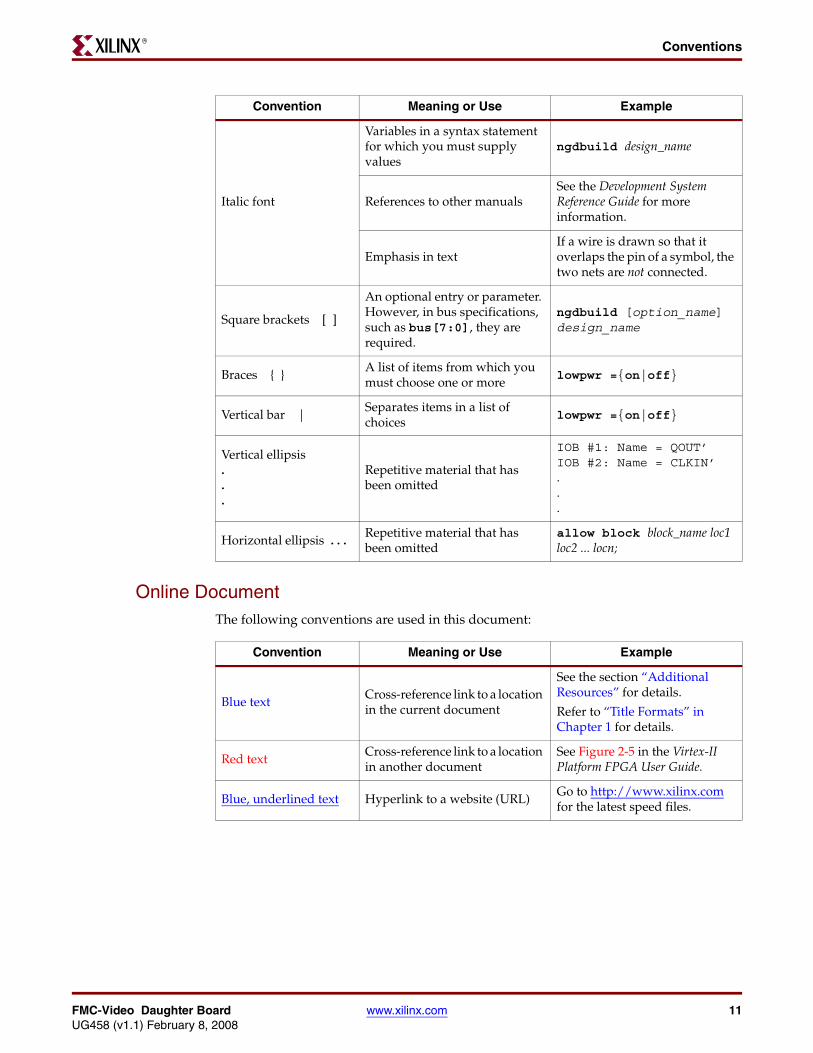
ConventionsThis document uses the following conventions. An example illustrates each convention.
TypographicalThe following typographical conventions are used in this document:
FMC FPGA Mezzanine Card Standard (VITA-57.1)
FPGA Field Programmable Gate Array
I2C/I2C Inter-Integrated Circuit
IC Integrated Circuit
LED Light Emitting Diode
LVDS Low Voltage Differential Signaling
MSPS Mega-Samples Per Second
NTSC National Television System Committee (SDTV broadcast standard originating from U.S.)
PAL Phase Alternating Line (international SDTV broadcast standard)
PC Personal Computer
SDTV Standard Definition Television
SECAM Sequential Couleur Avec Memoire (French) (sequential color with memory) (An international SDTV broadcast standard originating from France)
TMDS Transition Minimized Differential Signaling
VITA VMEbus International Trade Association
VGA Video Graphics Array
VSK Spartan-3A DSP Video Starter Kit
Convention Meaning or Use Example
Courier fontMessages, prompts, and program files that the system displays
speed grade: - 100
Courier boldLiteral commands that you enter in a syntactical statement
ngdbuild design_name
Helvetica bold
Commands that you select from a menu
File → Open
Keyboard shortcuts Ctrl+C
FMC-Video Daughter Board www.xilinx.com 11UG458 (v1.1) February 8, 2008
ConventionsR
Online DocumentThe following conventions are used in this document:
Italic font
Variables in a syntax statement for which you must supply values
ngdbuild design_name
References to other manualsSee the Development System Reference Guide for more information.
Emphasis in textIf a wire is drawn so that it overlaps the pin of a symbol, the two nets are not connected.
Square brackets [ ]
An optional entry or parameter. However, in bus specifications, such as bus[7:0], they are required.
ngdbuild [option_name] design_name
Braces { }A list of items from which you must choose one or more
lowpwr ={on|off}
Vertical bar |Separates items in a list of choices
lowpwr ={on|off}
Vertical ellipsis...
Repetitive material that has been omitted
IOB #1: Name = QOUT’ IOB #2: Name = CLKIN’...
Horizontal ellipsis . . .Repetitive material that has been omitted
allow block block_name loc1 loc2 ... locn;
Convention Meaning or Use Example
Convention Meaning or Use Example
Blue textCross-reference link to a location in the current document
See the section “Additional Resources” for details.
Refer to “Title Formats” in Chapter 1 for details.
Red textCross-reference link to a location in another document
See Figure 2-5 in the Virtex-II Platform FPGA User Guide.
Blue, underlined text Hyperlink to a website (URL)Go to http://www.xilinx.com for the latest speed files.
12 www.xilinx.com FMC-Video Daughter BoardUG458 (v1.1) February 8, 2008
Preface: About This GuideR
THIS PAGE LEFT BLANK INTENTIONALLY.
FMC-Video Daughter Board www.xilinx.com 13UG458 (v1.1) February 8, 2008
R
Chapter 1
Introduction
The FMC-Video is a hardware daughter board that includes video interfaces and the circuitry necessary for connection to an FPGA device via a daughter card connector on the carrier board. The carrier/daughter board interface is intended to follow the VITA-57.1 FPGA Mezzanine Card (FMC) standard. This board is part of the Spartan-3A DSP Video Starter Kit (VSK) for firmware development and serves as a hardware reference design.
Hardware DependenciesThe specific carrier platform that is currently validated to support the FMC-Video daughter card is the Spartan-3A DSP FPGA 3400A Development Platform (Part number HW-SD3400A-DSP-DB-UNI-G). See www.xilinx.com for details.
14 www.xilinx.com FMC-Video Daughter BoardUG458 (v1.1) February 8, 2008
Chapter 1: IntroductionR
THIS PAGE LEFT BLANK INTENTIONALLY.
FMC-Video Daughter Board www.xilinx.com 15UG458 (v1.1) February 8, 2008
R
Chapter 2
Hardware Overview
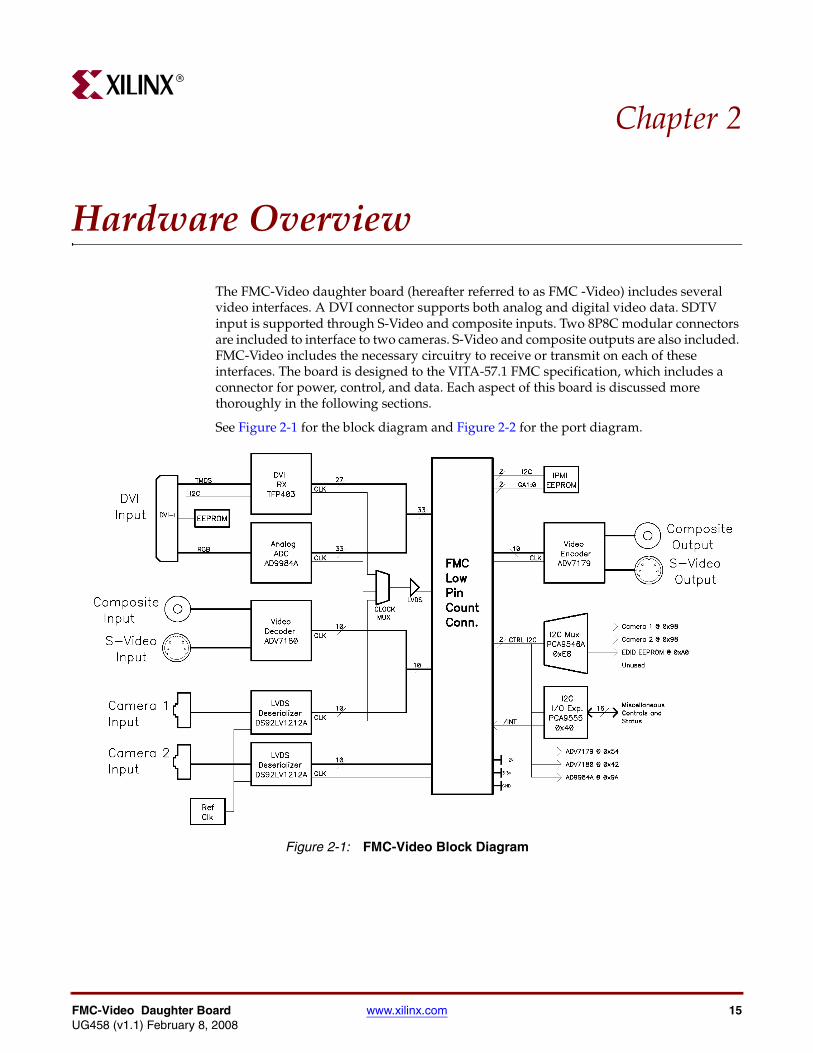
The FMC-Video daughter board (hereafter referred to as FMC -Video) includes several video interfaces. A DVI connector supports both analog and digital video data. SDTV input is supported through S-Video and composite inputs. Two 8P8C modular connectors are included to interface to two cameras. S-Video and composite outputs are also included. FMC-Video includes the necessary circuitry to receive or transmit on each of these interfaces. The board is designed to the VITA-57.1 FMC specification, which includes a connector for power, control, and data. Each aspect of this board is discussed more thoroughly in the following sections.
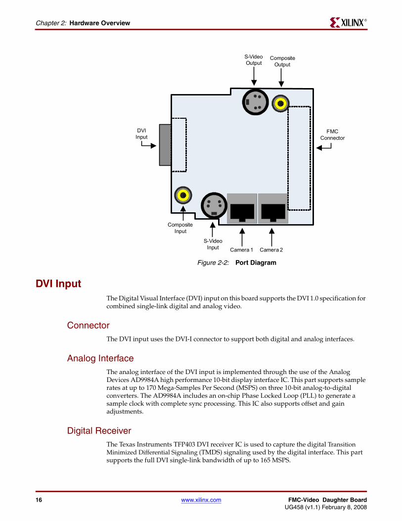
See Figure 2-1 for the block diagram and Figure 2-2 for the port diagram.X-Ref Target - Figure 2-1
Figure 2-1: FMC-Video Block Diagram
16 www.xilinx.com FMC-Video Daughter BoardUG458 (v1.1) February 8, 2008
Chapter 2: Hardware OverviewR
DVI InputThe Digital Visual Interface (DVI) input on this board supports the DVI 1.0 specification for combined single-link digital and analog video.
ConnectorThe DVI input uses the DVI-I connector to support both digital and analog interfaces.
Analog InterfaceThe analog interface of the DVI input is implemented through the use of the Analog Devices AD9984A high performance 10-bit display interface IC. This part supports sample rates at up to 170 Mega-Samples Per Second (MSPS) on three 10-bit analog-to-digital converters. The AD9984A includes an on-chip Phase Locked Loop (PLL) to generate a sample clock with complete sync processing. This IC also supports offset and gain adjustments.
Digital ReceiverThe Texas Instruments TFP403 DVI receiver IC is used to capture the digital Transition Minimized Differential Signaling (TMDS) signaling used by the digital interface. This part supports the full DVI single-link bandwidth of up to 165 MSPS.
X-Ref Target - Figure 2-2
Figure 2-2: Port Diagram
s
s
Camera 2Camera 1S-Video
Input
CompositeInput
S-VideoOutput
Composite Output
DVIInput
FMC Connector
FMC-Video Daughter Board www.xilinx.com 17UG458 (v1.1) February 8, 2008
Composite/S-Video InputR
DDC-EDIDThe DVI input supports identification through the use of an Extended Display Identification Data (EDID) structure available through the Display Data Channel (DDC) interface. This consists of an I2C EEPROM that is powered through the DVI connector and accessible through the connector. The FMC-Video board also includes the ability to access this EEPROM internally for programming it, as outlined in the “Control I2C” section.
Composite/S-Video Input
ConnectorsThis video interface is provided via two connectors: a female DIN 4 connector for S-Video and an RCA phone jack for composite signals. The pinout for the S-Video connector is given in Table 2-1. These connectors are industry standard.
Video DecoderThe Analog Devices ADV7180 10-bit 4x over-sampling SDTV Video Decoder IC is used to receive and digitize the composite or S-video input. This part can automatically detect and convert standard analog baseband television signals, including National Television System Committee (NTSC), Phase Alternating Line (PAL), and Sequential Couleur Avec Memoire (Fr.) (SECAM). The output of this device is 4:2:2 8-bit component video data.
Camera InputsFMC-Video includes two camera interfaces to allow the capture of data from two cameras simultaneously. The camera is a custom camera based on a Micron MT9V022 Digital CMOS image sensor.
ConnectorThe camera interface is based on an RJ45 connector using a proprietary pinout. At the moment the only camera that can be used with this connector is the one that is designed for the Xilinx VSK. The pinout for this connector is given in Table 2-2.
Table 2-1: S-Video Port Pinout
Pin Number Signal
1 Ground (Y)
2 Ground (C)
3 Intensity (Luminance)
4 Color (Chrominance)
Table 2-2: Camera Connector Pinout
Pin Number Signal Name Direction
1 LVDS_P In
2 LVDS_N In
3 CLK_P In
18 www.xilinx.com FMC-Video Daughter BoardUG458 (v1.1) February 8, 2008
Chapter 2: Hardware OverviewR
Warning: The RJ45 connectors on FMC-Video are not Ethernet ports. Connecting anything other than the camera supplied with VSK to these ports could result in damage to your equipment.
DeserializerThe data stream from the camera is in the form of a high-speed LVDS data stream. This stream is received and deserialized using a National DS92LV1212A deserializer. This is capable of carrying LVDS data from a camera which has a pixel rate of 26.6 MHz.
The deserializer requires a reference clock that is provided via a fixed-frequency 27 MHz oscillator.
Composite/S-Video Output
ConnectorsThis video interface is provided via two connectors: a female DIN 4 connector for S-Video and an RCA phone jack for composite signals. These connectors are industry standard.
Video EncoderThe Analog Devices ADV7179 PAL/NTSC Video Encoder IC is used to drive the S-Video output. This part is given 8-bit 4:2:2 component video data. The pixel clock frequency is generated by the carrier.
I2C BusesFMC-Video includes two completely separate I2C buses. One is defined by the FMC specification, the other is for general control of components on the carrier card.
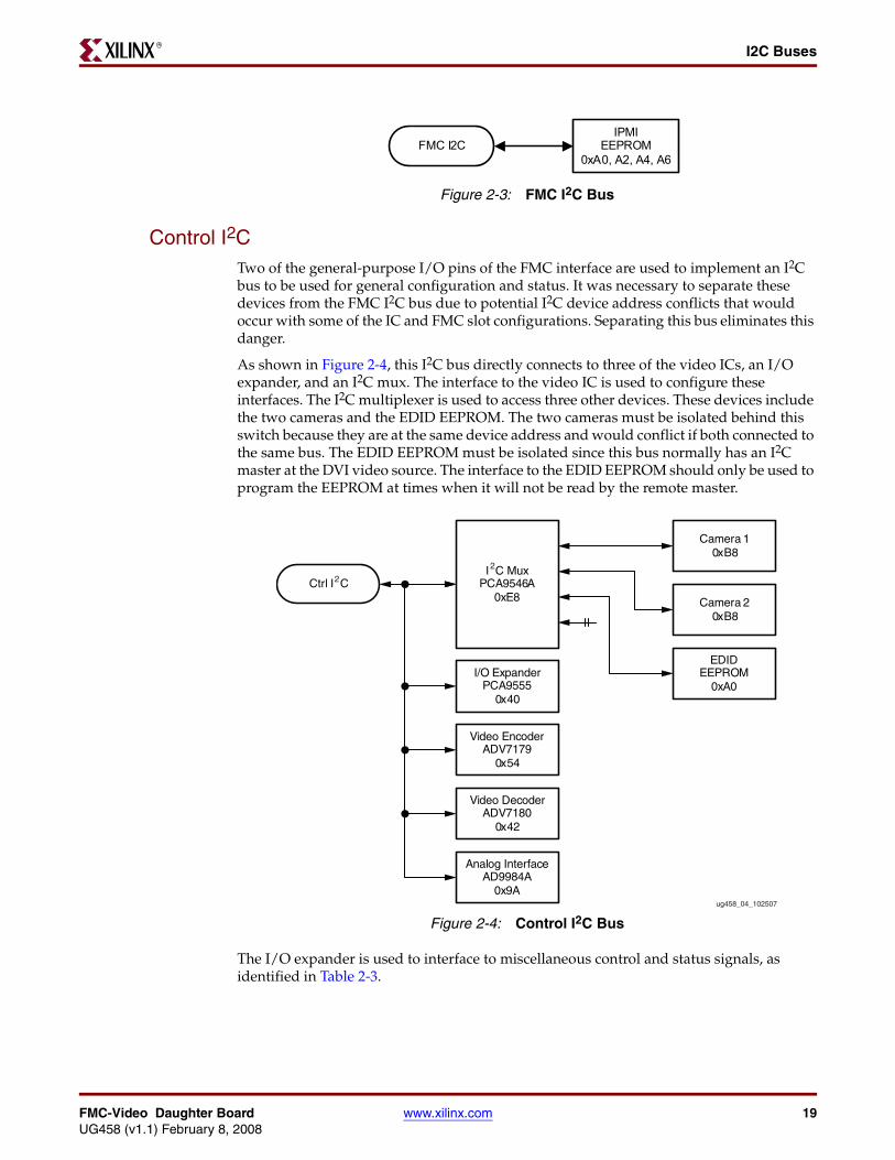
FMC I2CThe FMC specification includes an I2C bus as part of the interface. The mezzanine card is required to include an EEPROM that is read by the carrier card to identify and configure the interface for the mezzanine card. The only device connected to this I2C bus is this EEPROM, which is powered by the 3P3VAUX power supply.
4 VCC (5V) Out
5 SCL I/O
6 CLK_N In
7 SDA I/O
8 GND -
Table 2-2: Camera Connector Pinout (Cont’d)
Pin Number Signal Name Direction
FMC-Video Daughter Board www.xilinx.com 19UG458 (v1.1) February 8, 2008
I2C BusesR
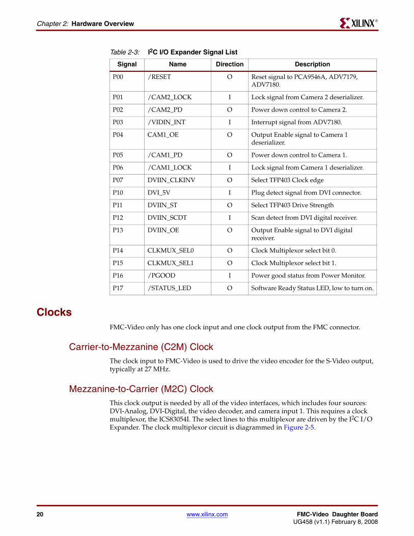
Control I2CTwo of the general-purpose I/O pins of the FMC interface are used to implement an I2C bus to be used for general configuration and status. It was necessary to separate these devices from the FMC I2C bus due to potential I2C device address conflicts that would occur with some of the IC and FMC slot configurations. Separating this bus eliminates this danger.
As shown in Figure 2-4, this I2C bus directly connects to three of the video ICs, an I/O expander, and an I2C mux. The interface to the video IC is used to configure these interfaces. The I2C multiplexer is used to access three other devices. These devices include the two cameras and the EDID EEPROM. The two cameras must be isolated behind this switch because they are at the same device address and would conflict if both connected to the same bus. The EDID EEPROM must be isolated since this bus normally has an I2C master at the DVI video source. The interface to the EDID EEPROM should only be used to program the EEPROM at times when it will not be read by the remote master.
The I/O expander is used to interface to miscellaneous control and status signals, as identified in Table 2-3.
X-Ref Target - Figure 2-3
Figure 2-3: FMC I2C Bus
IPMIEEPROM
0xA0, A2, A4, A6FMC I2C
X-Ref Target - Figure 2-4
Figure 2-4: Control I2C Bus
I/O ExpanderPCA9555
0x40
Video EncoderADV7179
0x54
Video DecoderADV7180
0x42
Analog InterfaceAD9984A
0x9A
Camera 10xB8
Camera 20xB8
EDIDEEPROM
0xA0
I C MuxPCA9546A
0xE8Ctrl I C2
2
ug458_04_102507
20 www.xilinx.com FMC-Video Daughter BoardUG458 (v1.1) February 8, 2008
Chapter 2: Hardware OverviewR
ClocksFMC-Video only has one clock input and one clock output from the FMC connector.
Carrier-to-Mezzanine (C2M) ClockThe clock input to FMC-Video is used to drive the video encoder for the S-Video output, typically at 27 MHz.
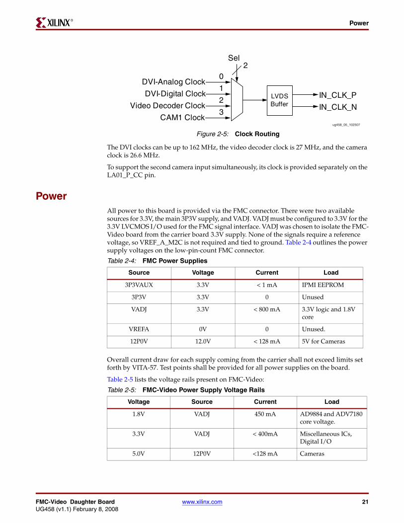
Mezzanine-to-Carrier (M2C) ClockThis clock output is needed by all of the video interfaces, which includes four sources: DVI-Analog, DVI-Digital, the video decoder, and camera input 1. This requires a clock multiplexor, the ICS83054I. The select lines to this multiplexor are driven by the I2C I/O Expander. The clock multiplexor circuit is diagrammed in Figure 2-5.
Table 2-3: I2C I/O Expander Signal List
Signal Name Direction Description
P00 /RESET O Reset signal to PCA9546A, ADV7179, ADV7180.
P01 /CAM2_LOCK I Lock signal from Camera 2 deserializer.
P02 /CAM2_PD O Power down control to Camera 2.
P03 /VIDIN_INT I Interrupt signal from ADV7180.
P04 CAM1_OE O Output Enable signal to Camera 1 deserializer.
P05 /CAM1_PD O Power down control to Camera 1.
P06 /CAM1_LOCK I Lock signal from Camera 1 deserializer.
P07 DVIIN_CLKINV O Select TFP403 Clock edge
P10 DVI_5V I Plug detect signal from DVI connector.
P11 DVIIN_ST O Select TFP403 Drive Strength
P12 DVIIN_SCDT I Scan detect from DVI digital receiver.
P13 DVIIN_OE O Output Enable signal to DVI digital receiver.
P14 CLKMUX_SEL0 O Clock Multiplexor select bit 0.
P15 CLKMUX_SEL1 O Clock Multiplexor select bit 1.
P16 /PGOOD I Power good status from Power Monitor.
P17 /STATUS_LED O Software Ready Status LED, low to turn on.
FMC-Video Daughter Board www.xilinx.com 21UG458 (v1.1) February 8, 2008
PowerR
The DVI clocks can be up to 162 MHz, the video decoder clock is 27 MHz, and the camera clock is 26.6 MHz.
To support the second camera input simultaneously, its clock is provided separately on the LA01_P_CC pin.
PowerAll power to this board is provided via the FMC connector. There were two available sources for 3.3V, the main 3P3V supply, and VADJ. VADJ must be configured to 3.3V for the 3.3V LVCMOS I/O used for the FMC signal interface. VADJ was chosen to isolate the FMC-Video board from the carrier board 3.3V supply. None of the signals require a reference voltage, so VREF_A_M2C is not required and tied to ground. Table 2-4 outlines the power supply voltages on the low-pin-count FMC connector.
Overall current draw for each supply coming from the carrier shall not exceed limits set forth by VITA-57. Test points shall be provided for all power supplies on the board.
Table 2-5 lists the voltage rails present on FMC-Video:
X-Ref Target - Figure 2-5
Figure 2-5: Clock Routing
DVI-Analog Clock
DVI-Digital Clock
Video Decoder ClockIN_CLK_P
2Sel
CAM1 ClockIN_CLK_N
LVDS Buffer
0
1
2
3ug458_05_102507
Table 2-4: FMC Power Supplies
Source Voltage Current Load
3P3VAUX 3.3V < 1 mA IPMI EEPROM
3P3V 3.3V 0 Unused
VADJ 3.3V < 800 mA 3.3V logic and 1.8V core
VREFA 0V 0 Unused.
12P0V 12.0V < 128 mA 5V for Cameras
Table 2-5: FMC-Video Power Supply Voltage Rails
Voltage Source Current Load
1.8V VADJ 450 mA AD9884 and ADV7180 core voltage.
3.3V VADJ < 400mA Miscellaneous ICs, Digital I/O
5.0V 12P0V <128 mA Cameras
22 www.xilinx.com FMC-Video Daughter BoardUG458 (v1.1) February 8, 2008
Chapter 2: Hardware OverviewR
Analog and digital power supplies are isolated using ferrites and proper grounding layout.
Signal Bus MultiplexingBecause of the large number of signals required by each of the video interfaces and the limited number of signals on the FMC connector, it is not possible to dedicate a connector pin for each of the data bits. To fit within the connector signal count, some signals must be shared. Rather than using traditional bus multiplexor ICs, which add cost, board space, and latency to the signals, some of the signals can be multiplexed by sharing nets and controlling the signal output enables. This was done with two pairs of data buses.
DVI Bus MultiplexingThe DVIIN_x signals are shared between the DVI analog interface and the DVI digital receiver. The DVI receiver outputs are high-impedance when the PDO_L pin is asserted Low. This pin is controlled by the DVIIN_OE signal on the I2C I/O expander. The default of this is Low, not enabled. The outputs of the DVI analog interface, the AD9884A, can be disabled through its I2C control registers. Its default state is output enabled. To prevent bus contention, only one of these interfaces can be enabled at a time.
Note: The data width from the analog interface is 10 bits, while the data width from the digital receiver is only 8 bits. This means that two of the bits are not shared. These signals were connected such that the two devices use the same bit as the most significant bit, bit 9. The digital receiver does not use bits 1 and 0.
Video Input MultiplexingThe VIDIN_x signals are shared between the video decoder and camera 1. The camera 1 signals are set to high impedance using the REN pin on the deserializer, driven by the net CAM1_OE, from the I2C I/O expander. The default state is Low, not enabled. The outputs of the video decoder, the ADV7180, are disabled through its I2C control registers. The default state is enabled. To prevent bus contention only one of these interfaces can be enabled at a time.
FMC Low Pin Count Connector
Standard PinoutThe VITA-57 FMC connector is of the low-pin-count (LPC) variant. All I/O on this connector shall be 3.3V single ended, with the exception of two LVDS clocks. The available pins in the LPC connector are in rows C, D, G, and H, as shown in Figure 2-6.
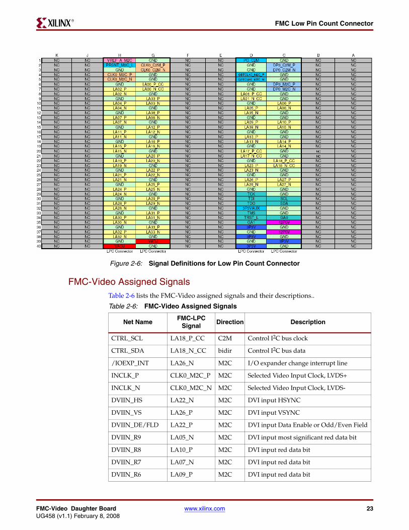
FMC-Video Daughter Board www.xilinx.com 23UG458 (v1.1) February 8, 2008
FMC Low Pin Count ConnectorR
FMC-Video Assigned SignalsTable 2-6 lists the FMC-Video assigned signals and their descriptions..
X-Ref Target - Figure 2-6
Figure 2-6: Signal Definitions for Low Pin Count Connector
Table 2-6: FMC-Video Assigned Signals
Net NameFMC-LPC
SignalDirection Description
CTRL_SCL LA18_P_CC C2M Control I2C bus clock
CTRL_SDA LA18_N_CC bidir Control I2C bus data
/IOEXP_INT LA26_N M2C I/O expander change interrupt line
INCLK_P CLK0_M2C_P M2C Selected Video Input Clock, LVDS+
INCLK_N CLK0_M2C_N M2C Selected Video Input Clock, LVDS-
DVIIN_HS LA22_N M2C DVI input HSYNC
DVIIN_VS LA26_P M2C DVI input VSYNC
DVIIN_DE/FLD LA22_P M2C DVI input Data Enable or Odd/Even Field
DVIIN_R9 LA05_N M2C DVI input most significant red data bit
DVIIN_R8 LA10_P M2C DVI input red data bit
DVIIN_R7 LA07_N M2C DVI input red data bit
DVIIN_R6 LA09_P M2C DVI input red data bit
24 www.xilinx.com FMC-Video Daughter BoardUG458 (v1.1) February 8, 2008
Chapter 2: Hardware OverviewR
DVIIN_R5 LA10_N M2C DVI input red data bit
DVIIN_R4 LA12_P M2C DVI input red data bit
DVIIN_R3 LA09_N M2C DVI input red data bit
DVIIN_R2 LA13_P M2C DVI input red data bit
DVIIN_R1 LA07_P M2C DVI input red data bit, 0 & 1 unused for digital mode
DVIIN_R0 LA06_N M2C DVI input least significant red data bit
DVIIN_G9 LA05_P M2C DVI input most significant green data bit
DVIIN_G8 LA06_P M2C DVI input green data bit
DVIIN_G7 LA11_P M2C DVI input green data bit
DVIIN_G6 LA12_N M2C DVI input green data bit
DVIIN_G5 LA11_N M2C DVI input green data bit
DVIIN_G4 LA13_N M2C DVI input green data bit
DVIIN_G3 LA16_P M2C DVI input green data bit
DVIIN_G2 LA16_N M2C DVI input green data bit
DVIIN_G1 LA04_N M2C DVI input green data bit, 0 & 1 unused for digital mode
DVIIN_G0 LA04_P M2C DVI input least significant green data bit
DVIIN_B9 LA15_P M2C DVI input most significant blue data bit
DVIIN_B8 LA17_P_CC M2C DVI input blue data bit
DVIIN_B7 LA15_N M2C DVI input blue data bit
DVIIN_B6 LA17_N_CC M2C DVI input blue data bit
DVIIN_B5 LA20_P M2C DVI input blue data bit
DVIIN_B4 LA23_P M2C DVI input blue data bit
DVIIN_B3 LA20_N M2C DVI input blue data bit
DVIIN_B2 LA23_N M2C DVI input blue data bit
DVIIN_B1 LA02_N M2C DVI input blue data bit, 0 & 1 unused for digital mode
DVIIN_B0 LA02_P M2C DVI input least significant blue data bit
VIDIN_HS LA21_N M2C Video input HSYNC or CAM1 Line
VIDIN_FLD/VS LA21_P M2C Video input FIELD/VSYNC or CAM1 Frame
VIDIN_D7 LA27_P M2C Video input most significant data bit
VIDIN_D6 LA27_N M2C Video input data bit
Table 2-6: FMC-Video Assigned Signals (Cont’d)
Net NameFMC-LPC
SignalDirection Description
FMC-Video Daughter Board www.xilinx.com 25UG458 (v1.1) February 8, 2008
FMC Low Pin Count ConnectorR
VIDIN_D5 LA25_P M2C Video input data bit
VIDIN_D4 LA25_N M2C Video input data bit
VIDIN_D3 LA24_P M2C Video input data bit
VIDIN_D2 LA24_N M2C Video input data bit
VIDIN_D1 LA29_P M2C Video input data bit
VIDIN_D0 LA29_N M2C Video input least significant data bit
CAM2_CLK LA01_P_CC M2C Camera 2 Input Clock
CAM2_LINE LA32_P M2C Camera 2 LINE
CAM2_FRAME LA32_N M2C Camera 2 Frame
CAM2_D7 LA33_N M2C Camera 2 most significant data bit
CAM2_D6 LA33_P M2C Camera 2 data bit
CAM2_D5 LA30_N M2C Camera 2 data bit
CAM2_D4 LA30_P M2C Camera 2 data bit
CAM2_D3 LA31_N M2C Camera 2 data bit
CAM2_D2 LA31_P M2C Camera 2 data bit
CAM2_D1 LA28_P M2C Camera 2 data bit
CAM2_D0 LA28_N M2C Camera 2 least significant data bit
VIDOUT_CLK CLK0_C2M_P C2M Video Output Clock
VIDOUT_HS LA19_N M2C Video output HSYNC
VIDOUT_FLD/VS LA19_P M2C Video output FIELD/VSYNC
VIDOUT_D7 LA14_N M2C Video output most significant data bit
VIDOUT_D6 LA14_P M2C Video output data bit
VIDOUT_D5 LA08_N M2C Video output data bit
VIDOUT_D4 LA08_P M2C Video output data bit
VIDOUT_D3 LA03_N M2C Video output data bit
VIDOUT_D2 LA03_P M2C Video output data bit
VIDOUT_D1 LA00_N_CC M2C Video output data bit
VIDOUT_D0 LA00_P_CC M2C Video output least significant data bit
Table 2-6: FMC-Video Assigned Signals (Cont’d)
Net NameFMC-LPC
SignalDirection Description
26 www.xilinx.com FMC-Video Daughter BoardUG458 (v1.1) February 8, 2008
Chapter 2: Hardware OverviewR
LEDsFMC-Video includes two status 2 LEDs, placed on the back of the board. These LEDs indicate that the board is being powered correctly and the software has initialized it, respectively. See Table 2-7.
MechanicalWherever possible this module conforms to VITA-57 from a mechanical standpoint. It is impossible to meet the mechanical specs due to the size of the connectors that must be on the board. For instance, all the connectors cannot fit within the I/O envelope height of 9.5 mm on the front of the board. Due to this, some connectors must be put on the back of the board. However, the orientation of these connectors should still support two FMC modules installed side by side on a carrier. To this end, all connectors are oriented toward the front panel side of the board or directly vertical.
Although the mechanical spec is broken by this design, it is possible for mechanical conformance to be achieved by simply removing the connectors that are placed on the back.
Rule 25 of the VITA-57 spec requires a minimum of 500 VDC and 1 MÙ of isolation. The only S-video connectors available for this application are rated at 250 VDC isolation and, therefore, violate this rule. Even with these connectors removed, there is still only 250 VDC isolation, because the spacing between pads on the PCB artwork to accommodate this connector.
Table 2-7: Board LEDs
Net Name FMC-LPC Signal Direction
1 PG Power supplies are within regulation
2 I2C I/O Expander Software initialization complete
FMC-Video Daughter Board www.xilinx.com 27UG458 (v1.1) February 8, 2008
R
Chapter 3
Tools and Files
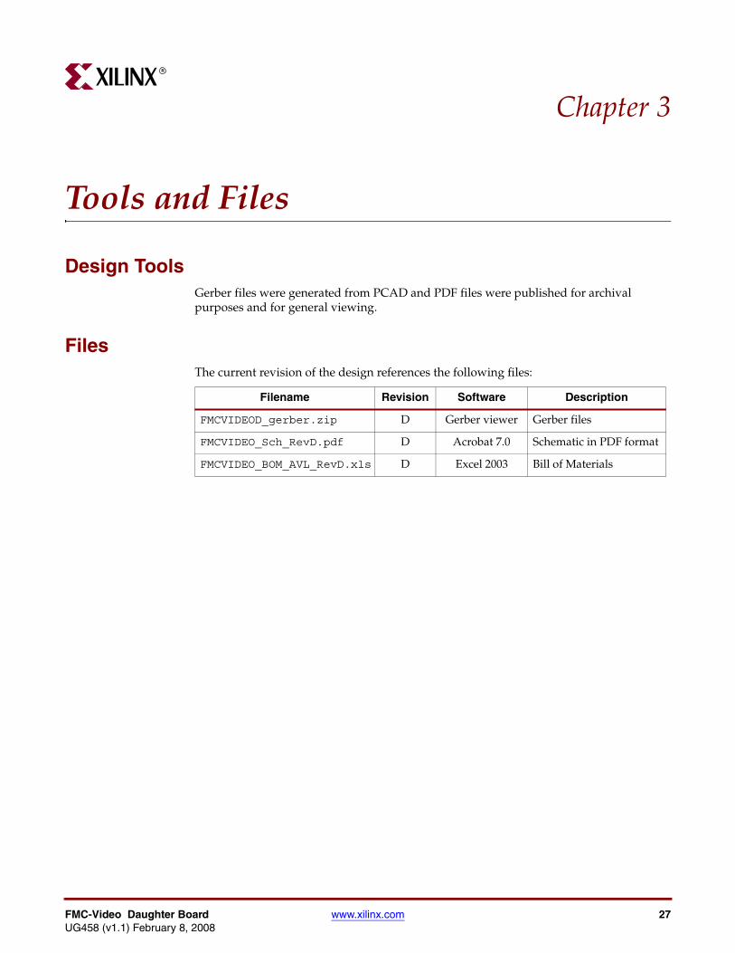
Design ToolsGerber files were generated from PCAD and PDF files were published for archival purposes and for general viewing.
FilesThe current revision of the design references the following files:
Filename Revision Software Description
FMCVIDEOD_gerber.zip D Gerber viewer Gerber files
FMCVIDEO_Sch_RevD.pdf D Acrobat 7.0 Schematic in PDF format
FMCVIDEO_BOM_AVL_RevD.xls D Excel 2003 Bill of Materials
28 www.xilinx.com FMC-Video Daughter BoardUG458 (v1.1) February 8, 2008
Chapter 3: Tools and FilesR
THIS PAGE LEFT BLANK INTENTIONALLY.
FMC-Video Daughter Board www.xilinx.com 29UG458 (v1.1) February 8, 2008
R
Chapter 4
Test Designs
This chapter covers the designs that are used for programming and testing the hardware.
Loopback DesignThis is an FPGA design for an FMC-Carrier board that tests the FMC-Video board interfaces by generating test patterns on outputs and testing them on inputs. This test uses a DVI digital and analog output on the carrier board as a test source.
Test Setup
Required Hardware
• FMC-Video installed on a Spartan-3A DSP FPGA 3400A Development Platform
• DVI-I Cable (analog and digital)
• S-Video Cable
• Composite Cable (RCA)
• Two Cameras, MT9V022
• Two Cat-6 cables with 8P8C modular connectors
DVI Loopback
The DVI-I cable connects the DVI output on the carrier board to the DVI input on FMC-Video.
S-Video Loopback
The S-Video cable connects the S-Video output on FMC-Video to the S-Video input on FMC-Video.
Composite Loopback
The composite (RCA) cable connects the Composite output on FMC-Video to the Composite input on FMC-Video.
Camera Test
The camera test is not a loopback. Instead, a camera is connected to each camera port using a Cat-6 cable.
30 www.xilinx.com FMC-Video Daughter BoardUG458 (v1.1) February 8, 2008
Chapter 4: Test DesignsR
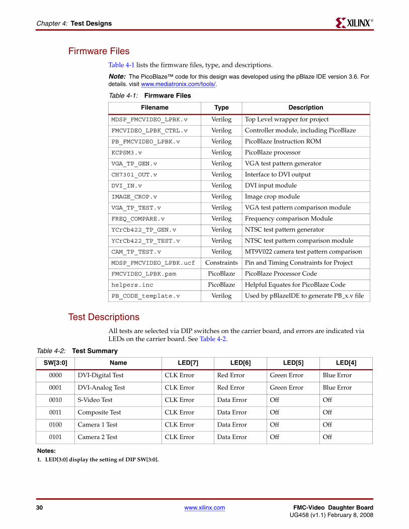
Firmware FilesTable 4-1 lists the firmware files, type, and descriptions.
Note: The PicoBlaze™ code for this design was developed using the pBlaze IDE version 3.6. For details. visit www.mediatronix.com/tools/.
Test DescriptionsAll tests are selected via DIP switches on the carrier board, and errors are indicated via LEDs on the carrier board. See Table 4-2.
Table 4-1: Firmware Files
Filename Type Description
MDSP_FMCVIDEO_LPBK.v Verilog Top Level wrapper for project
FMCVIDEO_LPBK_CTRL.v Verilog Controller module, including PicoBlaze
PB_FMCVIDEO_LPBK.v Verilog PicoBlaze Instruction ROM
KCPSM3.v Verilog PicoBlaze processor
VGA_TP_GEN.v Verilog VGA test pattern generator
CH7301_OUT.v Verilog Interface to DVI output
DVI_IN.v Verilog DVI input module
IMAGE_CROP.v Verilog Image crop module
VGA_TP_TEST.v Verilog VGA test pattern comparison module
FREQ_COMPARE.v Verilog Frequency comparison Module
YCrCb422_TP_GEN.v Verilog NTSC test pattern generator
YCrCb422_TP_TEST.v Verilog NTSC test pattern comparison module
CAM_TP_TEST.v Verilog MT9V022 camera test pattern comparison
MDSP_FMCVIDEO_LPBK.ucf Constraints Pin and Timing Constraints for Project
FMCVIDEO_LPBK.psm PicoBlaze PicoBlaze Processor Code
helpers.inc PicoBlaze Helpful Equates for PicoBlaze Code
PB_CODE_template.v Verilog Used by pBlazeIDE to generate PB_x.v file
Table 4-2: Test Summary
SW[3:0] Name LED[7] LED[6] LED[5] LED[4]
0000 DVI-Digital Test CLK Error Red Error Green Error Blue Error
0001 DVI-Analog Test CLK Error Red Error Green Error Blue Error
0010 S-Video Test CLK Error Data Error Off Off
0011 Composite Test CLK Error Data Error Off Off
0100 Camera 1 Test CLK Error Data Error Off Off
0101 Camera 2 Test CLK Error Data Error Off Off
Notes: 1. LED[3:0] display the setting of DIP SW[3:0].
FMC-Video Daughter Board www.xilinx.com 31UG458 (v1.1) February 8, 2008
Loopback DesignR
DVI-Digital
The DVI output on the carrier board generates a VGA test pattern of red, green, and blue ramps. This is received by FMC-Video and is compared against what was sent. To pass this test, the received clock frequency must be correct and the test pattern must be received with no errors.
DVI-Analog
The DVI output on the carrier board generates a VGA test pattern of red, green, and blue ramps. This is received by FMC-Video and is compared against what was sent. To pass this test, the received clock frequency must be correct and the test pattern must closely match the test pattern. Since this is an analog interface, the digitized version will never perfectly match the sent image, so some error is acceptable. To pass, the majority of the pixels must be within a small error range of the test pattern value.
S-Video
The S-Video output on the carrier board generates an NTSC test pattern of red, green, and blue ramps. This is received by FMC-Video and is compared against what was sent. To pass this test, the received clock frequency must be correct and the test pattern must closely match the test pattern. Since this is an analog interface, the digitized version will never perfectly match the sent image, so some error is acceptable. To pass, the majority of the pixels must be within a small error range of the test pattern value.
Composite
The composite output on the carrier board generates an NTSC test pattern of red, green, and blue ramps. This is received by FMC-Video and is compared against what was sent. To pass this test, the received clock frequency must be correct and the test pattern must closely match the test pattern. Since this is an analog interface, the digitized version will never perfectly match the sent image, so some error is acceptable. To pass, the majority of the pixels must be within a small error range of the test pattern value.
Camera 1
The camera is configured to generate a test pattern. This is received by FMC-Video and is compared against what the test pattern is supposed to be. To pass this test, the received clock frequency must be correct and the test pattern must be received with no errors.
Camera 2
This test is the same as Camera 1.
32 www.xilinx.com FMC-Video Daughter BoardUG458 (v1.1) February 8, 2008
Chapter 4: Test DesignsR
Pass-Through DesignThis is an FPGA design for an FMC-Carrier board that tests the FMC-Video board interfaces by passing video data through the carrier board FPGA. This test uses a DVI digital and analog output on the carrier board as an output.
Test Setup
Required Hardware
• FMC-Video installed on Spartan-3A DSP FPGA 3400A Development Platform
• Composite/S-Video source (for example, DVD player)
• Composite/S-Video display (for example, TV)
• DVI-I source (for example, PC)
• DVI-I display (for example, LCD computer monitor)
• Τwo DVI-I Cables (analog and digital)
• Two S-Video Cables
• Two Composite Cables (RCA)
• Two Cameras, MT9V022
• Two Cat-6 cables with 8P8C modular connectors
DVI Pass-Through
One DVI-I cable connects the DVI output on the carrier board to the DVI-I display. The other DVI-I cable connects the DVI output of the DVI-I video source to the DVI input on FMC-Video.
S-Video Pass-Through
One S-Video cable connects the S-Video output on FMC-Video to the S-Video input on the Composite/S-Video display. The other S-Video cable connects the S-Video output on the Composite/S-Video source to the S-Video input on FMC-Video.
Composite Loopback
One composite (RCA) cable connects the composite output on FMC-Video to the composite input on the Composite/S-Video display. The second composite cable connects the composite output on the Composite/S-Video source to the composite input on FMC-Video.
Camera Test
One camera is connected to each camera port using a Cat-6 cable.
FMC-Video Daughter Board www.xilinx.com 33UG458 (v1.1) February 8, 2008
Pass-Through DesignR
Firmware FilesTable 4-3 lists the firmware files, type, and descriptions.
Note: The PicoBlaze code for this design was developed using the pBlaze IDE version 3.6. For details, visit http://www.mediatronix.com/tools/.
Mode DescriptionsAll modes are selected via DIP switches on the carrier board. See Table 4-4
Table 4-3: Firmware Files
Filename Type Description
MDSP_FMCVIDEO_PASS.v Verilog Top Level wrapper for project
FMCVIDEO_PASS_CTRL.v Verilog Controller module, including PicoBlaze
PB_FMCVIDEO_PASS.v Verilog PicoBlaze Instruction ROM
KCPSM3.v Verilog PicoBlaze processor
DVI_IN.v Verilog DVI input module
IMAGE_CROP.v Verilog Image crop module
YCrCb422_IN.v Verilog Video input module
MICRON_IMAGE_SENSOR_IN.v Verilog Micron Image Sensor Input module
YCrCb422_OUT.v Verilog Video Output Module
CH7301_OUT.v Verilog Interface to DVI output
MDSP_FMCVIDEO_PASS.ucf Constraints Pin and Timing Constraints for Project
FMCVIDEO_PASS.psm PicoBlaze PicoBlaze Processor Code
helpers.inc PicoBlaze Helpful Equates for PicoBlaze Code
PB_CODE_template.v Verilog Used by pBlazeIDE to generate PB_x.v file
Table 4-4: Mode Descriptions
SW[3:0] Name Input Output
0000 DVI-Digital <65 MHz DVI Digital DVI Digital & Analog
0001 DVI-Digital >65 MHz DVI Digital DVI Digital & Analog
0010 DVI-Analog VGA60 DVI Analog DVI Digital & Analog
0011 DVI-Analog SVGA60 DVI Analog DVI Digital & Analog
0100 DVI-Analog XGA60 DVI Analog DVI Digital & Analog
0101 DVI-Analog SXGA60 DVI Analog DVI Digital & Analog
0110 DVI-Analog UXGA60 DVI Analog DVI Digital & Analog
1000 Camera 1 Camera 1 DVI Digital & Analog
1001 Camera 2 Camera 2 DVI Digital & Analog
34 www.xilinx.com FMC-Video Daughter BoardUG458 (v1.1) February 8, 2008
Chapter 4: Test DesignsR
DVI-Digital
Modes 0 and 1 are both DVI-Digital input. The division at 65 MHz is required by the DVI output on the Carrier board. The captured data is output on the DVI output as both digital and analog.
DVI-Analog
Modes 2 through 6 are analog input. Each analog input resolution requires specific timing and crop settings. The captured data is output on the DVI output as both digital and analog.
Camera 1
The camera is configured and the data is captured by FMC-Video. The captured data is output on the DVI output as both digital and analog.
Camera 2
The camera is configured and the data is captured by FMC-Video. The captured data is output on the DVI output as both digital and analog.
S-Video
The Video decoder is configured to receive S-Video. This is passed to the video encoder and output as both S-Video and Composite.
Composite
The Video decoder is configured to receive Composite Video. This is passed to the video encoder and output as both S-Video and Composite.
1010 S-Video S-Video S-Video and Composite
1011 Composite Composite S-Video and Composite
Table 4-4: Mode Descriptions (Cont’d)
SW[3:0] Name Input Output