your optical coating experts
TRANSCRIPT

OPTOSIGMA
Your Optical Coating Experts

• Optical coatings enhance or reduce surface reflection• Uncoated N-BK7 glass loses ~4% per surface
• Typically 1 to over 100 layers of various materials• Alternating groups of higher and lower index materials• Either ¼-wave or ½-wave optical thickness layers
• Optical thickness = physical thickness x index of refraction
• Most basic antireflection coating is single ¼-wave layer Magnesium Fluoride or Silicon Dioxide• ½-wave used as protective layer on metallic mirrors
!"#$%&'%#(%)*$&+#,%-.#$&(/0

SUBSTRATE FEATURES• Aspect ratio• Longest dimension to thickness
• Surface quality• Print through• Stress point for single-layer coating
• Clear aperture
ENVIRONMENT• Temperature• Cryogenic v. hot• Large excursion
• Humidity• Radiation
OPTICAL DESIGN• Angle(s) of incidence• Extreme angles harder to design for
• Shift performance to longer wavelength
• Soft glass types v. hard• Broadband v. narrowband• Out of band blocking
SYSTEM REQUIREMENTS• Wavelength(s)• Laser power• Required Reflectance• High performance may require lower laser
damage threshold materials• Polarization sensitivity
123%42'&/(%-.('&526#$&.('
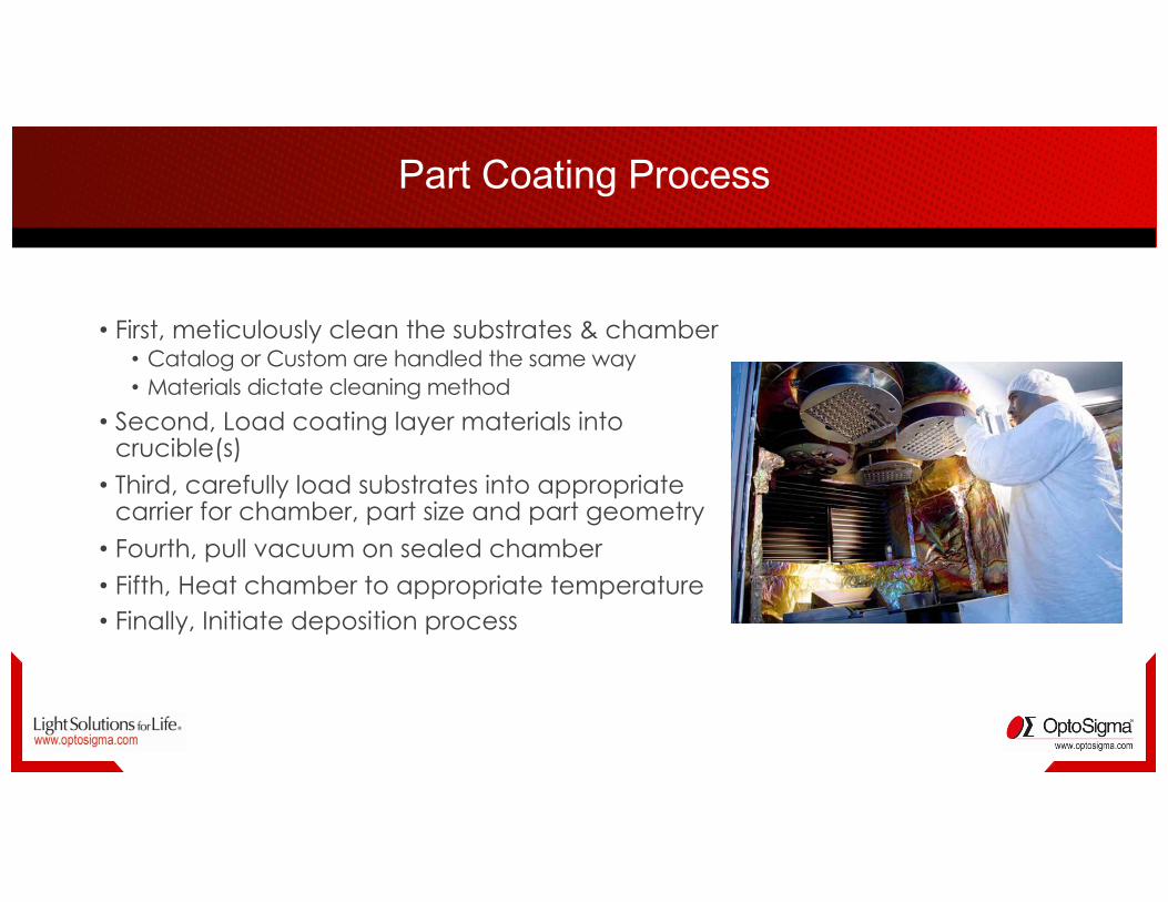
• First, meticulously clean the substrates & chamber• Catalog or Custom are handled the same way• Materials dictate cleaning method
• Second, Load coating layer materials into crucible(s)• Third, carefully load substrates into appropriate
carrier for chamber, part size and part geometry• Fourth, pull vacuum on sealed chamber• Fifth, Heat chamber to appropriate temperature• Finally, Initiate deposition process
7#6$%-.#$&(/%76.+2''

• Depends on the number of layers• Single layer coating is fastest• Very broadband AR coating takes the longest
• Can be > 100 layers
• Overall performance and tolerances• Transmission/Reflection
• Absolute (P-V) or average (RMS)• Transition requirements
• Width of transition zone• No instantaneous transitions
• Number of layers• Single band v. multi band
• Also depends on number & size of substrates
8.9%:.(/%4.2'%76.+2''%;#<20

• 100+ make to order standard coating recipes available!• Working WL Range: 248nm-2700nm• Antireflection
• All Dielectric• V-coat, U-Coat, W-Coat• High Laser Damage Threshold (LDT)• Low Temperature Process Capability
• Reflection• All Dielectric• Single band, Broadband
• Dichroics• Short-Wave and Long-Wave Pass
• ITAR Registered
)*$.=&/>#%?=@%-#*#A&,&$&2'

• High Finesse and Low Loss Coatings• Standard Catalog Items and Custom• Super Mirrors: R<99.999% - 8PPM• Development for six 9’s and 1PPM Ongoing!
• Ultrafast Mirror Coatings• Low and Negative Dispersion (GDD)• Standard Catalog Items and Custom
• Antireflection• Filter• Polarization• Ultra-Broadband**Coating for Flight and Space Applications
)*$.=&/>#%B,.A#,%-#*#A&,&$&2'
Ultra Broadband
Super Mirrors

Electron Beam Deposition (EBeam)• Charged tungsten filament gives off
electron beam which bombards target anode• Anode - crucible of coating layer
material• Gaseous material from crucible deposits
in solid layer on everything in line of sight
)*$.=&/>#%-.#$&(/%C2$".5' !"#$%#&'

Ion Assisted Deposition (IAD)•Material deposition assisted by ion
source• Increases mobility of molecules or atoms
• Increased grain size• Increased density• Optimized step coverage
Plasma Assisted Deposition (PAD)•Material deposition assisted by
Plasma source• Much higher particle kinetic energy
• Greater molecule impact energy• Increased density
)*$.=&/>#%-.#$&(/%C2$".5' !(#$%#&'

Ion Beam Sputtering•Creates more dense film layers• Increased durability• Higher performance coatings• Improved deposition uniformity
• Tighter packing of molecules and atoms•More available materials
)*$.=&/>#%-.#$&(/%C2$".5' !&#$%#&'

DE%F.G%-#(H$%C2#'G62%D$I%F.G%-#(H$%C#<2%D$J

!.6,59&52%-.#$&(/%-#*#A&,&$&2'
è OptoSigma (California) is ITAR Registered
• 44+ years of experience
• Applications include Space Rated, Bio-Medical, Semiconductor, Sensing, High Power and much more!• 25+ coating chambers• E-Beam w/ IAD and IBS Chambers
• Substrate size: 3 to 400 mm• (1-Meter Online in 2021)
• Catalog or custom
• ISO 9001:2015 and 14001:2015

;"#(<%3.GJ
We appreciate your interest in the coating capabilities of our
family of companies. Please contact us with any questions or
projects.
We strive to be cost effective!
Eastern & Southern US:Chris [email protected]