zero defects guideline - aecouncil.com defects guideline ... system engineering (user) quality...
TRANSCRIPT

DRAFT AEC - Q004
August 31, 2006
ZERO DEFECTS GUIDELINE
Component Technical CommitteeAutomotive Electronics Council

DRAFT AEC – Q004
August 31, 2006
Component Technical CommitteeAutomotive Electronics Council
Acknowledgment Any document involving a complex technology brings together experience and skills from many sources. The Automotive Electronics Council would especially like to recognize the following significant contributors to the revision of this document:
Sustaining Members: Mark A. Kelly Delphi Corporation Jean Clarac Siemens VDO Brian Jendro Siemens VDO Robert V. Knoell Visteon Corporation Associate Members: Guest Members: Tim Haifley Altera David Locker AMRDEC Daniel Vanderstraeten AMI Semiconductor Jeff Jarvis AMRDEC Earl Fischer Autoliv Mike Klucher Cirrus Logic Xin Miao Zhao Cirrus Logic John Timms Continental Automotive Systems Roy Ozark Continental Automotive Systems Nick Lycoudes Freescale Werner Kanert Infineon Technologies Elfriede Geyer Infineon Technologies John Bertaux International Rectifier Gary Fisher Johnson Controls Tom Lawler Lattice Semiconductor Mike Buzinski Microchip Rob Horton Microchip Annette Nettles NEC Electronics Raj Radjassamay NEC Electronics Mark Gabrielle ON Semiconductor Zhongning Liang Philips Semiconductor Ken Berry Renesas Technology Bruce Townsend Spansion Adam Fogle Spansion Brian Mielewski STMicroelectronics James Williams Texas Instruments Diana Siddall Texas Instruments Don Pecko Xilinx Other Contributors: Masachi Murase NEC Electronics Michael Wieberneit NEC Electronics David Lehtonen Spansion Romeo Letor STMicroelectronics Sebastiano Russo STMicroelectronics

DRAFT AEC – Q004
August 31, 2006
Component Technical CommitteeAutomotive Electronics Council
NOTICE
AEC documents contain material that has been prepared, reviewed, and approved through the AEC Technical Committee. AEC documents are designed to serve the automotive electronics industry through eliminating misunderstandings between manufacturers and purchasers, facilitating interchangeability and improvement of products, and assisting the purchaser in selecting and obtaining with minimum delay the proper product for use by those other than AEC members, whether the standard is to be used either domestically or internationally. AEC documents are adopted without regard to whether or not their adoption may involve patents or articles, materials, or processes. By such action AEC does not assume any liability to any patent owner, nor does it assume any obligation whatever to parties adopting the AEC documents. The information included in AEC documents represents a sound approach to product specification and application, principally from the automotive electronics system manufacturer viewpoint. No claims to be in Conformance with this document may be made unless all requirements stated in the document are met. Inquiries, comments, and suggestions relative to the content of this AEC document should be addressed to the AEC Technical Committee on the link http://www.aecouncil.com. Published by the Automotive Electronics Council. This document may be downloaded free of charge, however AEC retains the copyright on this material. By downloading this file the individual agrees not to charge for or resell the resulting material. Printed in the U.S.A. All rights reserved Copyright © 2006 by Delphi, Siemens VDO, and Visteon Corporation. This document may be freely reprinted with this copyright notice. This document cannot be changed without approval by the AEC Components Technical Committee.
DRAFT AEC – Q004
August 31, 2006
Component Technical CommitteeAutomotive Electronics Council
Page 3 of 55
ZERO DEFECTS GUIDELINE The proposed DRAFT of AEC-Q004 is made available for a 6-month industry review period, scheduled to expire on April 1, 2007. All comments and suggested edits should be made by contacting the AEC Technical Committee (http://www.aecouncil.com/AECRequest.html). After the 6-month review period has expired, all received comments and suggestions will be reviewed by the Technical Committee and incorporated (where applicable) into a final version of the Q004 document. 1. SCOPE
This document describes and organizes a set of tools and processes which suppliers and users of integrated circuits can use to approach or achieve the goal of zero defects during a product's lifetime. This guideline makes suggestions for when each of these tools and methods should be used depending on the application or business case. This is not to be construed as a requirements document, but is a tool box of methods that have been used to reduce defects. This is not an exhaustive list. There are suppliers that are using internally developed and proprietary methods to reduce defects. As the part and/or process is optimized and matures over time, less tools are needed to improve or maintain quality and reliability.
1.1 Purpose
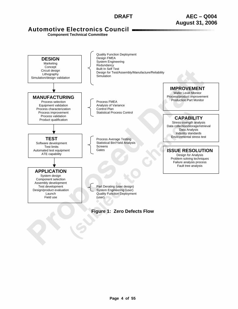
The flowchart below describes the sequence of steps involved in component design, manufacture, test and use and where each of the zero defect tool or method fits in with this component flow. Each tool or method is described along with how it addresses zero defects, when it would or wouldn't be used, the estimated cost versus benefit, the components and technologies it applies to, the defect type addressed and the metric used to measure performance.
DRAFT AEC – Q004
August 31, 2006
Component Technical CommitteeAutomotive Electronics Council
Page 4 of 55
Figure 1: Zero Defects Flow
IMPROVEMENT Wafer Level Monitor
Process/product improvementProduction Part Monitor
CAPABILITY Stress-strength analysis
Data collection/storage/retrievalData Analysis
Industry standards Environmental stress test
ISSUE RESOLUTIONDesign for Analysis
Problem solving techniques Failure analysis process
Fault tree analysis
DESIGN Marketing Concept
Circuit design Lithography
Simulation/design validation
Quality Function Deployment Design FMEA System Engineering Redundancy Built In Self Test Design for Test/Assembly/Manufacture/ReliabilitySimulation
MANUFACTURING Process selection
Equipment validation Process characterization
Process improvement Process validation
Product qualification
Process FMEA Analysis of Variance Control Plan Statistical Process Control
TEST Software development
Test limits Automated test equipment
ATE capability
Process Average Testing Statistical Bin/Yield AnalysisScreens Gates
APPLICATION System design
Component selection Assembly development
Test development Design/product evaluation
Launch Field use
Part Derating (user design) System Engineering (user) Quality Function Deployment (user)

DRAFT AEC – Q004
August 31, 2006
Component Technical CommitteeAutomotive Electronics Council
Page 5 of 55
1.2 Reference Documents
• AEC-Q100: Stress Test Qualification for Integrated Circuits • AEC-Q101: Stress Test Qualification for Discrete Semiconductors • AEC-Q100-009: Electrical Distribution Assessment • AEC-Q001: Guidelines for Part Average Testing • AEC-Q002: Guidelines for Statistical Yield Analysis • APQP-2: Advanced Product Quality Planning & Control Plan • EIA 659: Failure Mechanism Driven Reliability Monitoring • EIA-557-A: Statistical Process Control Systems • FMEA-3: Potential Failure Modes & Effects Analysis, AIAG • JESD50A: Special Requirements for Maverick Product Elimination • JEP13A: Guideline for Constant Temperature Aging to Characterize Aluminum Interconnect Method
for Stress Migration Induced Voiding • JEP119A: A Procedure For Executing SWEAT • JEP122B: Failure Mechanisms and Models for Silicon Semiconductor Devices • JEP131A: Process Failure Modes & Effects Analysis • JEP148: Reliability Qualification of Semiconductor Devices Based Upon Physics of Failure Risks and
Applications Assessments • JEP150: Stress Test Drive Qualification of and Failure Mechanisms Associated With Assembled Solid
State Surface Mount Components • JESD16-a: Assessment of Average Outgoing Quality Levels in Parts Per Million (PPM) • JESD35: Procedure for Wafer Level Testing of Thin Dielectrics • JESD671: Component Quality Problem Analysis and Corrective Action Requirements • JESD74: Early Life Failure Rate Calculation Procedure for Electronic Components • JESD94: Application Specific Qualification Using Knowledge Based Test Methodology • JESD659: Failure Mechanism Driven Reliability Monitoring • SPC-3: Statistical Process Control, AIAG • JEDEC JESD-46 Customer Notification of Product/Process Changes by Semiconductor Suppliers

DRAFT AEC – Q004
August 31, 2006
Component Technical CommitteeAutomotive Electronics Council
Page 6 of 55
LIST OF REFERENCES Sect# Tool AEC JEDEC AIAG SAE IEC Other 3.1 4.1
Failure Mode and Effect Analysis (FMEA)
FMEA-3 JEP131
3.2 Redundancy
3.3 5.2
Built-in Self Test
3.4 5.1
Design for Test
3.5 8.1
Design for Analysis
3.6 Design for Manufacture
3.7 Design for Reliability JEP148
3.8 Simulation JEP122 JEP148
3.9 Characterization AEC-Q003 AEC-Q100-009
4.2 Statistical Analysis of Variance
4.3 Control Plan APQP-2
4.4 Statistical Process Control EIA557 SPC-3
5.3 Process/Part Average Testing AEC-Q001
5.4 Statistical Bin Yield Analysis AEC-Q002
5.5 Data Collection, Storage and Retrieval
5.6 Screens JESD50 JESD16 JESD74
MIL-PRF-19500 MIL-STD-883
5.7 Lot Acceptance Gates JESD50 JESD16 JESD74
6.1 Stress-Strength Analysis
6.2 Data Analysis
6.3 Industry Standards
6.4 Environmental Stress Testing AEC-Q100 AEC-Q101 AEC-Q200
JESD22 JESD94 JEP150
6.5 Part Derating
7.1 Wafer Level Failure Mechanism Monitoring
7.2 Process/Product Improvements
AEC-Q100 JESD46
7.3 Production Part Monitoring EIA/JESD659
8.2 Problem Solving Techniques JESD671
8.3 Failure Analysis Process JESD671
8.4 Fault Tree Analysis
9.1 System Engineering
9.2 Quality Function Deployment
1.3 Definitions
Data mining – automating the process of searching for patterns in a data set. Ongoing defect – typically a common cause or intrinsic failure that follows a trend Spike defect – typically a special cause or extrinsic failure that occurs infrequently NTF – No trouble found TNI – Trouble not identified

DRAFT AEC – Q004
August 31, 2006
Component Technical CommitteeAutomotive Electronics Council
Page 7 of 55
2. RECOMMENDATIONS Precommended/needed O may be used O not recommended/needed
Sect Tool All new parts at
the design stage
High complexity
part
Low complexity
part
Fully mature or near
obsolescent component
Cost sensitive part or
application
Design or
process change
Issue or
failure occurs
Low reliability
application
High reliability or safety critical
application
3.1 4.1
Failure Mode and Effect Analysis FMEA
P O O O O P P O P
3.2 Redundancy O P O O O O O O P 3.3 5.2
Built-in Self Test O P O O O O P O P
3.4 5.1
Design for Test P P O O O P P O P
3.5 8.1
Design for Analysis O P O O O O P O P
3.6 Design for Manufacture O O O O O P P O P 3.7 Design for Reliability O O O O O O P O P 3.8 Simulation P P O O P O P O P 3.9 Characterization P P O O O P O O P 4.2 Statistical Analysis of
Variance O O
O
O O
O
P O
O
4.3 Control Plan O O O O O P O O P 4.4 Statistical Process
Control P P P P P P P P P
5.3 Process/Part Average Testing
P O
O
O O
O
O
O P
5.4 Statistical Bin Yield Analysis P O
O O O
O
O O P
5.5 Data Collection, Storage and Retrieval
O
O
O
P O
P P O
O
5.6 Screens P P P P P P P P P 5.7 Lot Acceptance Gates O P O P P O O P O
6.1 Stress-Strength Analysis O P O O O O O O P 6.2 Data Analysis P P P P P P P P P 6.3 Industry Standards P P P P P P P P P 6.4 Environmental Stress
Testing P P O O O
P O
O P
6.5 Part Derating P O P P O O O P O 7.1 Wafer Level Fail
Mechanism Monitoring P O
O
O
O O
O
O P
7.2 Process/Product Improvements
O
O
O O O P P O
P
7.3 Production Part Monitoring
O
O
O
O O O
O
O P
8.2 Problem Solving Techniques
O O O O O P P O O
8.3 Failure Analysis Process O O O O O P P O O
8.4 Fault Tree Analysis O O O O O P P O O
9.1 System Engineering P O O O O O O O O
9.2 Quality Function Deployment P O O O O O O O O

DRAFT AEC – Q004
August 31, 2006
Component Technical CommitteeAutomotive Electronics Council
Page 8 of 55
3. DESIGN 3.1 Failure Mode and Effect Analysis (FMEA) 3.1.1 Description
A process performed by subject experts that identifies potential failure modes and their effects on the system and customer, determines their severity, occurrence and detection, and identifies possible causes and controls. The FMEA document identifies the risks associated with something potentially going wrong (creating a defect - out of specification) in the production of the product. The FMEA identifies what controls are placed in the production process to catch any defects at various stages on the processing. This applies both to process and design (product) FMEAs. The FMEA is essentially a collection of lessons learned from other related processes and products.
3.1.2 Where this fits in the material flow DFMEAs are performed on all new components and systems before design of component or
arrangement of process flow. DFMEAs are also updated for all design changes. This is a living document that can change upon new lessons learned and should be periodically reviewed for accuracy or relevance.
3.1.3 Components and technologies this applies to and how it addresses zero defects DFMEAs identify all potential modes of failure in design, their risks and how to control them. 3.1.4 Limitations Not intended for use with a product that is fully mature or is entering obsoletion. 3.1.5 Estimated cost versus benefit Cost includes man-hours to generate the expert knowledge document and uncertainty to new
unknown failure mechanisms/modes. Benefit includes prioritizing the circuit or process step most susceptible to part failure in order to improve it and communicating learning throughout the organization.
3.1.6 Defect type addressed (ongoing or spike) Ongoing (controllable) and spike (extrinsic) defects based on lessons learned. 3.1.7 Metrics used and meaning of values Risk priority number (product of severity, occurrence and detection) used to pareto which failure mode
or mechanism is most influential to product failure. 3.1.8 References
FMEA-3: Potential Failure Modes & Effects Analysis, AIAG 3.1.9 Examples Example of a FMEA is shown in figure 4.1a

DRAFT AEC – Q004
August 31, 2006
Component Technical CommitteeAutomotive Electronics Council
Page 9 of 55
3.2 Redundancy 3.2.1 Description
A parallel system of duplicate cells or components that can replace faulty ones seamlessly during the final test or actual use of a part. Redundancy can greatly increase the part’s mean time to failure. Another form of redundancy is error correction code to avoid latent data retention errors.
3.2.2 Where this fits in the material flow Used during design and test of logic, memory (e.g., flash, OTP), etc. 3.2.3 Components and technologies this applies to and how it addresses zero defects Greatly reduces failure rates via robust design (transparent cell replacement), and may reduce both 0
km (time zero) and field failure rates. Use for critical memory and application functions or when die size percentage increase is small or low cost vs. benefit.
3.2.4 Limitations Design or performance restrictions may inhibit the use of redundancy. Not intended for use with low
complexity or mature devices. Not to be used for low lifetime applications or where cost per die size is critical.
3.2.5 Estimated cost versus benefit Cost includes added circuitry, overhead support, and software. Benefit includes much improved
reliability. 3.2.6 Defect type addressed (ongoing or spike) Both ongoing and spike defects. 3.2.7 Metrics used and meaning of values Yield and number of customer returns. 3.2.8 References
3.2.9 Examples Example of redundancy in a memory array:

DRAFT AEC – Q004
August 31, 2006
Component Technical CommitteeAutomotive Electronics Council
Page 10 of 55
3.3 Built-in Self Test 3.3.1 Description
The practice of designing the circuitry such that inputting a logic solution will allow the part to test itself.
3.3.2 Where this fits in the material flow Intended for use with high complexity components and is designed into the product. 3.3.3 Components and technologies this applies to and how it addresses zero defects Provides the device with the capability of diagnosing itself for process or design errors which
otherwise might go undetected through the development stage. This includes functions or parametrics internal to the device that are not accessible from the outside.
3.3.4 Limitations Not intended for use with low complexity parts. May be possible to switch off and not use as the part
and process matures. May increase die size and software code. 3.3.5 Estimated cost versus benefit Cost includes added circuitry and software. Benefit includes improved fault coverage over the die. 3.3.6 Defect type addressed (ongoing or spike) Ongoing (controllable) and spike (extrinsic) defects. 3.3.7 Metrics used and meaning of values Defect detectability and test coverage 3.3.8 References
3.3.9 Examples Example of a BIST circuit block and test program is shown in figure 3.3a

DRAFT AEC – Q004
August 31, 2006
Component Technical CommitteeAutomotive Electronics Council
Page 11 of 55
3.4 Design for Test 3.4.1 Description
The practice of designing the circuitry such that as many nodes as possible can be tested in a reasonable amount of time.
3.4.2 Where this fits in the material flow Intended for use with high complexity components and is designed into the product. 3.4.3 Components and technologies this applies to and how it addresses zero defects Provides the capability for testing as many nodes as possible and, thus, providing maximum fault
coverage during test. 3.4.4 Limitations Not intended for use with low complexity parts. 3.4.5 Estimated cost versus benefit Cost includes layout complexity, potential design time increase, and test software development.
Benefit includes more efficient defect screening. 3.4.6 Defect type addressed (ongoing or spike) Ongoing (controllable) and spike (extrinsic) defects. 3.4.7 Metrics used and meaning of values Test coverage, reduced incidence of NPF/TNI, and improved cycle time. 3.4.8 References
3.4.9 Examples Example of a test program with percent fault coverage and test time is shown in figure 3.4a
DRAFT AEC – Q004
August 31, 2006
Component Technical CommitteeAutomotive Electronics Council
Page 12 of 55
3.5 Design for Analysis 3.5.1 Description
The practice of designing the circuitry such that failure analysis can be performed as efficiently as possible for elimination of no defect found.
3.5.2 Where this fits in the material flow Intended for use with all components having a large number of metal layers or unique interconnection
schemes (e.g., chip-on-chip). Designed into the product. 3.5.3 Components and technologies this applies to and how it addresses zero defects Provides the capability of a more accurate and accessible analysis of failures which otherwise could
be masked by the proliferation of materials and features over the failed site. 3.5.4 Limitations Not intended for use with low complexity parts (few metal levels). 3.5.5 Estimated cost versus benefit Cost includes layout complexity and potential design time increase. Benefit includes easier and more
efficient failure analysis. 3.5.6 Defect type addressed (ongoing or spike) Ongoing (controllable) and spike (extrinsic) defects. 3.5.7 Metrics used and meaning of values Reduced cycle time for FA and reduced incidence of NPF/TNI. 3.5.8 References
3.5.9 Examples Example of chip designs allowing for DFA is shown in figure 3.5a

DRAFT AEC – Q004
August 31, 2006
Component Technical CommitteeAutomotive Electronics Council
Page 13 of 55
3.6 Design for Manufacture 3.6.1 Description
The practice of designing the circuitry so that the part can be more easily manufactured via larger design margins. These designs are intended to reduce the effects of extrinsic defects on the device, such as particulates and process margins (e.g., lithography definition).
3.6.2 Where this fits in the material flow Intended for use in new processes or sub-processes, new technology, new material sets or subsets
and new fab or assembly sites. 3.6.3 Components and technologies this applies to and how it addresses zero defects Examples include doubling (redundant) vias in areas that are process sensitive (e.g., sparse areas of
vias), widen spacing between interconnect lines, reduce the number of critical timing paths using synthesis tools.
3.6.4 Limitations Not intended for use in standard parts or processes and mature processes and technologies. 3.6.5 Estimated cost versus benefit Cost includes increased die area to accommodate design margin techniques (e.g., redundant vias).
Benefit includes reduced manufacturing defects (increased yield). 3.6.6 Defect type addressed (ongoing or spike) Ongoing (controllable) and spike (extrinsic) defects. 3.6.7 Metrics used and meaning of values Manufacturing yield, process control improvement 3.6.8 References
3.6.9 Examples Example of design margin for DFM is shown in figure 3.6a Figure 3.6a - Redundant vias in place of isolated ones

DRAFT AEC – Q004
August 31, 2006
Component Technical CommitteeAutomotive Electronics Council
Page 14 of 55
3.7 Design for Reliability 3.7.1 Description
Relaxation of design rules without sacrificing performance. The use of physics of failure to determine design and material limitations. Use of computer-aided engineering (CAE) analysis and simulation tools at an early stage in the design can improve product reliability more inexpensively and in a shorter time than building and testing physical prototypes. Tools such as finite element analysis, fluid flow, thermal analysis, integrated reliability prediction models, etc., are becoming more widely used, more user friendly and less expensive. Design of Experiments techniques can provide a structured, proactive approach to improving reliability and robustness as compared to unstructured, reactive design/build/test approaches. Further, these techniques consider the effect of both product and process parameters on the reliability of the product and address the effect of interactions between parameters. Finally, the company should begin establishing a mechanism to accumulate and apply "lessons learned" from the past related to reliability problems as well as other producibility and maintainability issues. These lessons learned can be very useful in avoiding making the same mistakes twice.
3.7.2 Where this fits in the material flow Intended for use in new part designs or processes, parts designed for new applications, applications
requiring high reliability. 3.7.3 Components and technologies this applies to and how it addresses zero defects Provides the capability of more rapid evaluation of reliability risks and the opportunity to mitigate them
early in the design process instead of after pre-development. Eliminating or minimizing the opportunity for mistakes to occur in manufacturing can be done early in the design process.
3.7.4 Limitations Not intended for use in standard designs or processes. 3.7.5 Estimated cost versus benefit Cost includes risk of lower reliability if the models and simulations are wrong, computer and software
overhead, time and cost needed to perform design of experiments, expertise in failure mechanisms. Benefits include a reduction in material needed for validation, faster cycle time, higher reliability if the models and simulation are right.
3.7.6 Defect type addressed (ongoing or spike) Ongoing (controllable) and spike (extrinsic) defects. 3.7.7 Metrics used and meaning of values Mean time to failure, warranty returns. 3.7.8 References
JEP13A: Guideline for Constant Temperature Aging to Characterize Aluminum Interconnect Method for Stress Migration Induced Voiding JEP119A: A Procedure For Executing SWEAT JEP148: Reliability Qualification of Semiconductor Devices Based Upon Physics of Failure Risks and Applications Assessments JESD35: Procedure for Wafer Level Testing of Thin Dielectrics http://www.npd-solutions.com/lifecycle.html
3.7.9 Examples
• Design based on the expected range of the operating environment. • Design to minimize or balance stresses and thermal loads and/or reduce sensitivity to these stresses
or loads.

DRAFT AEC – Q004
August 31, 2006
Component Technical CommitteeAutomotive Electronics Council
Page 15 of 55
• De-rate components for added margin. • Provide subsystem redundancy. • Use proven component parts & materials with well-characterized reliability. • Reduce parts count & interconnections (and their failure opportunities). • Improve process capabilities to deliver more reliable components and assemblies.

DRAFT AEC – Q004
August 31, 2006
Component Technical CommitteeAutomotive Electronics Council
Page 16 of 55
3.8 Simulation 3.8.1 Description
Recreating the functioning of the component through computer modeling using established engineering and physics-based relationships to functionality, construction and reliability.
3.8.2 Where this fits in the material flow Performed on all components during the design phase and possibly during the evaluation phase.
May be used during production to aid in debug or failure analysis (FA). Simulation should ALWAYS be used for every significant silicon pass.
3.8.3 Components and technologies this applies to and how it addresses zero defects Verifies functional operation of the device in addition to highlighting process, voltage and temperature
sensitivities related directly to the design and process parametrics. 3.8.4 Limitations Not intended for use after the component has been ramped up to full production (i.e., after initial
release of the product). It may not always be needed in determining production yield issues or FA. 3.8.5 Estimated cost versus benefit Irrelevant during the design phase as it is impossible to design without simulation. May be slightly
different if trying to use simulation as means to identify process or modeling issues. Cost includes running and analyzing data, and Q&R simulation program development/purchase. Benefit includes mitigating defects in design that otherwise would promulgate to manufacturing.
3.8.6 Defect type addressed (ongoing or spike) Both ongoing and spike defects. 3.8.7 Metrics used and meaning of values Direct simulation of specified parameters and functions. Parameter fit to empirical data, confidence
bound. 3.8.8 References
JEP122B: Failure Mechanisms and Models for Silicon Semiconductor Devices JEP148: Reliability Qualification of Semiconductor Devices Based Upon Physics of Failure Risks and Applications Assessments
3.8.9 Examples Example of a simulation is shown in figure 3.8a
DRAFT AEC – Q004
August 31, 2006
Component Technical CommitteeAutomotive Electronics Council
Page 17 of 55
3.9 Characterization 3.9.1 Description
The process of collecting and analyzing data in order to understand the attributes, behavior and limitations of a process, product design and the package. The characterization is performed to generate the specification or datasheet for the product, process or package. Intent is to look at parametric performance of the device with temperature, voltage, frequency, etc. Characterized parts, generated either via corner lot processing or sorted as extreme parametric values, can then be applied to the application to determine sensitive process corners that the supplier can either shift or tighten the process away from or sort out at test.
3.9.2 Where this fits in the material flow Typically performed on all new and changed components involving new designs or processes, at
wafer probe or final test. 3.9.3 Components and technologies this applies to and how it addresses zero defects Establishes the functional and parametric performance of the device by determining the electrical and
process parametric and performance limits. The "sweet spot" of the process is then fed back into manufacturing where it can be controlled.
3.9.4 Limitations Not intended for use after the component has been ramped up to full production (i.e., after initial
release of the product). 3.9.5 Estimated cost versus benefit Cost includes added testing for various parameters such as temperature, voltage, frequency, etc., and
manufacturing corner lots varying parameters such as Vtn, Vtp, CD, Rs, etc.. Benefit includes centering of the process, test versus the intended application, and establishing more accurate process and test limits.
3.9.6 Defect type addressed (ongoing or spike) Ongoing. 3.9.7 Metrics used and meaning of values Mean, minimum, maximum standard deviation, sample size, Cp, Cpk vs. datasheet or test limits,
temperature, voltage, frequency, and process corner variables (e.g., Vt, Leff, Rs, CD). Determines capability.
3.9.8 References
AEC-Q003 AEC-Q100-009: Electrical Distribution Assessment
3.9.9 Examples Example of a characterization is shown in figure 3.9a-d

DRAFT AEC – Q004
August 31, 2006
Component Technical CommitteeAutomotive Electronics Council
Page 18 of 55
COND. PARAMETER SPEC LO SPEC HI AVG STD DEV Cp Cpk1 R1 3300.00 6100.00 4568.16 348.43 1.34 1.211 R2 7000.00 13000.00 9488.32 744.22 1.34 1.111 R3 1400.00 3200.00 2656.39 68.18 4.40 6.141 R4 1400.00 3200.00 2626.69 55.62 5.39 7.351 VOH 0.50 1.00 0.78 0.00 55.45 61.621 VCEsat1 0.05 0.50 0.13 0.01 8.46 2.941 VCEsat2 0.05 0.50 0.21 0.01 6.12 4.261 VCEsat3 0.05 0.50 0.30 0.02 3.07 3.451 Hfe 100.00 500.00 143.20 7.18 9.29 2.01
Golden unit comparison from one test location versus another
Matrix Lot parameter range
Schmoo plot

DRAFT AEC – Q004
August 31, 2006
Component Technical CommitteeAutomotive Electronics Council
Page 19 of 55
4. MANUFACTURING 4.1 Failure Mode and Effect Analysis (FMEA) 4.1.1 Description
A process performed by subject experts that identifies potential failure modes and their effects on the system and customer, determines their severity, occurrence and detection, and identifies possible causes and controls. The FMEA document identifies the risks associated with something potentially going wrong (creating a defect - out of specification) in the production of the product. The FMEA identifies what controls are placed in the production process to catch any defects at various stages on the processing. This applies both to process and design (product) FMEAs.
4.1.2 Where this fits in the material flow Performed on all new components and systems before design of component or arrangement of
process flow. This is a living document that can change upon new lessons learned and should be periodically reviewed for accuracy or relevance.
4.1.3 Components and technologies this applies to and how it addresses zero defects Identifies all potential modes of failure in design and process, their risks and how to control them. 4.1.4 Limitations Not intended for use with a product that is fully mature or is entering obsoletion. 4.1.5 Estimated cost versus benefit Cost includes man-hours to generate the expert knowledge document and uncertainty to new
unknown failure mechanisms/modes. Benefit includes prioritizing the circuit or process step most susceptible to part failure in order to improve it, and communicating learning throughout the organization.
4.1.6 Defect type addressed (ongoing or spike) Ongoing (controllable) and spike (extrinsic) defects. 4.1.7 Metrics used and meaning of values Risk priority number (product of severity, occurrence and detection) used to pareto which failure mode
or mechanism is most influential to product failure. 4.1.8 References
FMEA-3: Potential Failure Modes & Effects Analysis, AIAG JEP131A: Process Failure Modes & Effects Analysis
4.1.9 Examples Example of a FMEA is shown in figure 4.1a

DRAFT AEC – Q004
August 31, 2006
Component Technical CommitteeAutomotive Electronics Council
Page 20 of 55
4.2 Statistical Analysis of Variance 4.2.1 Description
Mathematical procedure for determining the variables in a process that most influences the output characteristics of a given product depending on the manufacturing parameters.
4.2.2 Where this fits in the material flow Applicable anywhere in the process flow where data is collected for variation analysis and design of
experiments. 4.2.3 Components and technologies this applies to and how it addresses zero defects Methodology whose results can better target the optimal parameters of a device or process in order to
achieve optimum yield, function, and/or reliability. 4.2.4 Limitations Not intended for use with a product that is fully mature, is entering obsoletion, or if a failure never
occurs. 4.2.5 Estimated cost versus benefit Cost includes running the experiment and analyzing the data. Benefit includes improving the product
and/or process via optimized process/product parameters. 4.2.6 Defect type addressed (ongoing or spike) Ongoing (controllable) defects. 4.2.7 Metrics used and meaning of values Degrees of freedom, confounding, aliasing, correlation coefficient, and variables. 4.2.8 References
4.2.9 Examples Example of A DOE is shown in figure 4.2a

DRAFT AEC – Q004
August 31, 2006
Component Technical CommitteeAutomotive Electronics Council
Page 21 of 55
4.3 Control Plan 4.3.1 Description
A plan to control the product/process characteristics and the associated process variables to ensure capability (around the identified target or nominal) and stability of the product over time. For example, Cpk of critical characteristics of process measures stability over time.
4.3.2 Where this fits in the material flow
Performed for all manufacturing processes after the design of component, arrangement of process flow, and completion of the FMEA. This is a living document that can change upon new lessons learned and should be periodically reviewed for accuracy or relevance.
4.3.3 Components and technologies this applies to and how it addresses zero defects
Identifies the monitors, tests and screens that measure the performance of the process in the manufacture of the product. Specifies control criteria (e.g., use of X-bar-R chart, how to set control limits).
4.3.4 Limitations
None. 4.3.5 Estimated cost versus benefit
Cost includes man-hours to generate the document and translate the language across different locations. Benefit includes documenting the control monitors, methods of measurement, and test plans.
4.3.6 Defect type addressed (ongoing or spike)
Ongoing (controllable) and spike (extrinsic) defects. 4.3.7 Metrics used and meaning of values
Items to be recorded, observed, and measured, method of data analysis (e.g., Cpk, X-bar-R), equipment used for measurement/test, frequency of test, sample size, and datasheet or customer spec.
4.3.8 References
APQP-2: Advanced Product Quality Planning & Control Plan 4.3.9 Examples Example of a control plan is shown in figure 4.3a

DRAFT AEC – Q004
August 31, 2006
Component Technical CommitteeAutomotive Electronics Council
Page 22 of 55
4.4 Statistical Process Control 4.4.1 Description
Statistical process control (SPC) involves using statistical techniques to measure and analyze the variation in processes. Most often used for manufacturing processes, the intent of SPC is to monitor product quality and maintain processes to fixed targets. SPC is used to monitor the consistency of processes used to manufacture a product as designed. It aims to get and keep processes under control.
4.4.2 Where this fits in the material flow SPC can be used on all hardware components, software, and systems at any point in the
manufacturing process where variability exists and needs to be controlled. 4.4.3 Components and technologies this applies to and how it addresses zero defects One goal of SPC is to ensure process capability, which is a measure of the ability to consistently
produce to the required specifications without defects. Identification and control of random variation inherent within the process, as well as identification and elimination of special causes from external sources achieve this.
4.4.4 Limitations None. 4.4.5 Estimated cost versus benefit Identifying and removing process variations during design and/or manufacturing is a cost effective
way of defect prevention when compared to end-of-line screening. Poor production or screening yields, line-down situations, or warranty returns can result in un-budgeted costs that reach several thousands of dollars per hour. In addition, severe problems can easily drain a company's labor resources during problem investigation and resolution. Finally, the intangible cost of a damaged reputation and subsequent impact on future business opportunities is another major consideration for proactive elimination of defects. Adopting SPC tools during design and manufacturing not only helps to limit variation and associated costs, but also provides the measurable data necessary to promote a continuous improvement environment.
4.4.6 Defect type addressed (ongoing or spike) Both. SPC, once properly defined, can easily identify and control ongoing (trend) defect types as well
as short-term (spike) defect types. Performing periodic process capability studies also helps to identify unwanted 'special cause' defects that might be introduced at any time during the process.
4.4.7 Metrics used and meaning of values SPC has many metric values. Most common are the capability indices, Cp and Cpk. Cp, the process
capability index, defines a process in terms of its parameter spread with respect to the defined limits of a specification. It is a function of two variables, calculated as the width of the specification divided by the process spread. Cpk, the location index, indicates the location of the center of the actual distribution curve with respect to the target value. A Cpk > 1.33 should be maintained for most mature processes.
4.4.8 References
EIA-557-A: Statistical Process Control Systems SPC-3: Statistical Process Control, AIAG
4.4.9 Examples Example of a SPC control chart and statistics is shown in figure 4.4a-b
DRAFT AEC – Q004
August 31, 2006
Component Technical CommitteeAutomotive Electronics Council
Page 23 of 55
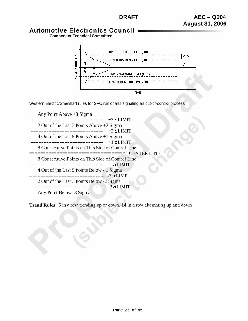
Western Electric/Shewhart rules for SPC run charts signaling an out-of-control process:
Any Point Above +3 Sigma --------------------------------------------- +3 LIMIT 2 Out of the Last 3 Points Above +2 Sigma --------------------------------------------- +2 LIMIT 4 Out of the Last 5 Points Above +1 Sigma --------------------------------------------- +1 LIMIT 8 Consecutive Points on This Side of Control Line =================================== CENTER LINE 8 Consecutive Points on This Side of Control Line --------------------------------------------- -1 LIMIT 4 Out of the Last 5 Points Below - 1 Sigma ---------------------------------------------- -2 LIMIT 2 Out of the Last 3 Points Below -2 Sigma --------------------------------------------- -3 LIMIT Any Point Below -3 Sigma
Trend Rules: 6 in a row trending up or down. 14 in a row alternating up and down

DRAFT AEC – Q004
August 31, 2006
Component Technical CommitteeAutomotive Electronics Council
Page 24 of 55
5. TEST 5.1 Design for Testability 5.1.1 Description
The practice of designing the circuitry such that as many nodes as possible can be tested in a reasonable amount of time. Conduct test plan reviews. Fault coverage of scan stuck-at and transition faults (AC scan: fault delay tests, transition delay tests, coupling faults), critical timing paths from static timing analysis, functional/speed patterns to test I/O interface, analog I/O patterns for voltage ramps and DC tests, drive strength and slew rates, customer application codes (user and supplier).
5.1.2 Where this fits in the material flow Intended for use with any high complexity component and is designed into the product. 5.1.3 Components and technologies this applies to and how it addresses zero defects Provides the capability for testing as many nodes as possible and, thus, providing maximum fault
coverage during test. 5.1.4 Limitations Not intended for use with low complexity parts 5.1.5 Estimated cost versus benefit Cost includes layout complexity, potential design time increase, and test software development.
Benefit includes more efficient defect screening. 5.1.6 Defect type addressed (ongoing or spike) Ongoing (controllable) and spike (extrinsic) defects. 5.1.7 Metrics used and meaning of values Test coverage, reduced incidence of NPF/TNI, and improved cycle time. 5.1.8 References
http://www.npd-solutions.com/lifecycle.html 5.1.9 Examples Example of a design and test program:
• Use of Geometric Dimensioning and Tolerancing (GD&T) to provide unambiguous representation of design intent
• Specification of product parameters and tolerances that are within the natural capabilities of the manufacturing process (process capability index Cp and Cpk)
• Provision of test points, access to test points and connections, and sufficient real estate to support test points, connections, and built-in test capabilities
• Standard connections and interfaces to facilitate use of standard test equipment and connectors and to reduce effort to setup and connect the product during testing
• Automated test equipment compatibility • Built-in test and diagnosis capability to provide self test and self-diagnosis in the factory and in the
field • Physical and electrical partitioning to facilitate test and isolation of faults

DRAFT AEC – Q004
August 31, 2006
Component Technical CommitteeAutomotive Electronics Council
Page 25 of 55
5.2 Built-in Self Test 5.2.1 Description
The practice of designing the circuitry such that inputting a logic solution will allow the part to test itself. Built-in Self Test, or BIST, is the technique of designing additional hardware and software features into integrated circuits to allow them to perform self-testing, i.e., testing of their own operation (functionally, parametrically, or both) using their own circuits, thereby reducing dependence on an external automated test equipment (ATE). BIST is a Design-for-Testability (DFT) technique, because it makes the electrical testing of a chip easier, faster, more efficient, and less costly. Checkerboard and inverse scan algorithms to detect bit-to-bit shorts and back-to-back reads. Address decoder fault algorithms to check for speed faults. SRAM and NVM bitmapping.
5.2.2 Where this fits in the material flow Intended for use with any high complexity component and is designed into the product. 5.2.3 Components and technologies this applies to and how it addresses zero defects Provides the device with the capability of diagnosing itself for process or design errors which
otherwise might go undetected through the development stage. This includes functions or parametrics internal to the device that are not accessible from the outside.
5.2.4 Limitations Not intended for use with low complexity parts. May be possible to switch off and not use as the part
and process matures. Issues that need to be considered when implementing BIST are: 1) faults to be covered by the BIST and how these will be tested for; 2) how much chip area will be occupied by the BIST circuits; 3) external supply and excitation requirements of the BIST; 4) test time and effectiveness of the BIST; 5) flexibility and changeability of the BIST (i.e., can the BIST be reprogrammed through an on-chip ROM?); 6) how the BIST will impact the production electrical test processes that are already in place
5.2.5 Estimated cost versus benefit Cost includes added circuitry and software. Benefit includes improved fault coverage over the die.
Advantages of implementing BIST include: 1) lower cost of test, since the need for external electrical testing using an ATE will be reduced, if not eliminated; 2) better fault coverage, since special test structures can be incorporated onto the chips; 3) shorter test times if the BIST can be designed to test more structures in parallel; 4) easier customer support; and 5) capability to perform tests outside the production electrical testing environment. The last advantage mentioned can actually allow the consumers themselves to test the chips prior to mounting or even after these are in the application boards. Disadvantages of implementing BIST include: 1) additional silicon area and fab processing requirements for the BIST circuits; 2) reduced access times; 3) additional pin (and possibly bigger package size) requirements, since the BIST circuitry need a way to interface with the outside world to be effective; and 4) possible issues with the correctness of BIST results, since the on-chip testing hardware itself can fail.
5.2.6 Defect type addressed (ongoing or spike) Ongoing (controllable) and spike (extrinsic) defects. 5.2.7 Metrics used and meaning of values Defect detectability and test coverage 5.2.8 References
http://www.semiconfareast.com/bist.htm http://www.quicklogic.com/images/appnote30.pdf

DRAFT AEC – Q004
August 31, 2006
Component Technical CommitteeAutomotive Electronics Council
Page 26 of 55
5.2.9 Examples Example of a BIST circuit and algorithm is shown in figure 5.2a
o Figure 1: Functional BIST principle

DRAFT AEC – Q004
August 31, 2006
Component Technical CommitteeAutomotive Electronics Council
Page 27 of 55
5.3 Process/Part Average Testing 5.3.1 Description
A system for designing, analyzing, and controlling manufacturing and test parameters of the device to ensure product quality. This method is designed to remove outliers from a given part population.
5.3.2 Where this fits in the material flow Performed on all new components and technologies at various points within and after the
manufacturing process. Can be used for electrical parametric testing in wafer probing and packaged final test.
5.3.3 Components and technologies this applies to and how it addresses zero defects Eliminates outliers from further production and shipment to customers. Provides early feedback on
initial release of product. 5.3.4 Limitations Continued for parts where it is being implemented. 5.3.5 Estimated cost versus benefit Cost includes performing variables testing on a sample of parts, inserting into test plan and increasing
test time, and removing outliers inside the spec limits. Benefit includes removing distribution outliers more likely to fail than main population and retargeting the test limits as the process matures.
5.3.6 Defect type addressed (ongoing or spike) Ongoing (controllable) and spike (extrinsic) defects. 5.3.7 Metrics used and meaning of values Cpk/Ppk versus datasheet or customer specification. 5.3.8 References
AEC-Q001: Guidelines for Part Average Testing 5.3.9 Examples Example of an outlier population is shown in figure 5.3a
DRAFT AEC – Q004
August 31, 2006
Component Technical CommitteeAutomotive Electronics Council
Page 28 of 55
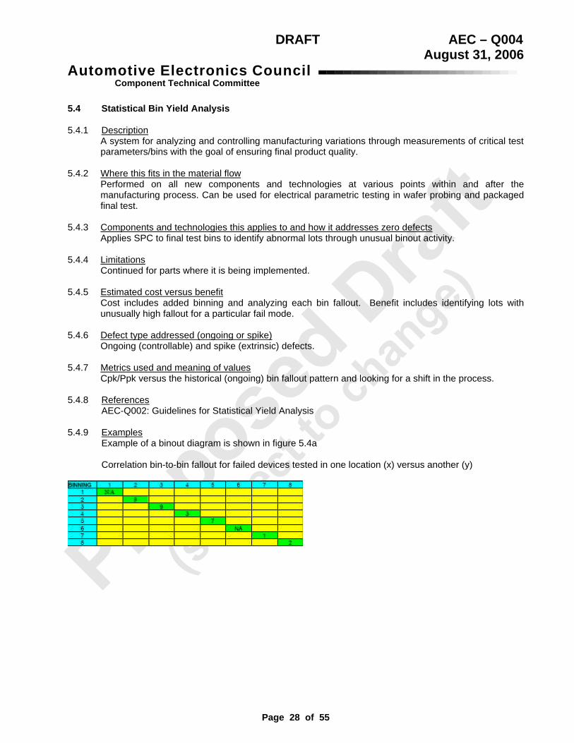
5.4 Statistical Bin Yield Analysis 5.4.1 Description
A system for analyzing and controlling manufacturing variations through measurements of critical test parameters/bins with the goal of ensuring final product quality.
5.4.2 Where this fits in the material flow Performed on all new components and technologies at various points within and after the
manufacturing process. Can be used for electrical parametric testing in wafer probing and packaged final test.
5.4.3 Components and technologies this applies to and how it addresses zero defects Applies SPC to final test bins to identify abnormal lots through unusual binout activity. 5.4.4 Limitations Continued for parts where it is being implemented. 5.4.5 Estimated cost versus benefit Cost includes added binning and analyzing each bin fallout. Benefit includes identifying lots with
unusually high fallout for a particular fail mode. 5.4.6 Defect type addressed (ongoing or spike) Ongoing (controllable) and spike (extrinsic) defects. 5.4.7 Metrics used and meaning of values Cpk/Ppk versus the historical (ongoing) bin fallout pattern and looking for a shift in the process. 5.4.8 References
AEC-Q002: Guidelines for Statistical Yield Analysis 5.4.9 Examples Example of a binout diagram is shown in figure 5.4a Correlation bin-to-bin fallout for failed devices tested in one location (x) versus another (y)

DRAFT AEC – Q004
August 31, 2006
Component Technical CommitteeAutomotive Electronics Council
Page 29 of 55
5.5 Data Collection, Storage and Retrieval 5.5.1 Description
The computational acquisition, archiving, cataloguing and rapid retrieval of data. This is used for rapid response to faulty quality and reliability metrics, to solve problems in the field possibly related to the part manufacture, or trends over time. Data mining is the analysis of correlations in the data that can lead to resolution of failure. Implementation of lessons learned from other products.
5.5.2 Where this fits in the material flow Intended for use with all components and technologies, anywhere where data can be obtained to
draw conclusions. Specific areas include spec revisions, qualification/PPAP, quality records, material traceability, process, test and customer return data.
5.5.3 Components and technologies this applies to and how it addresses zero defects Rapid availability of data speeds containment of issues. Allows rapid risk assessment. Benchmark
for quality improvement. 5.5.4 Limitations Must always be used. 5.5.5 Estimated cost versus benefit Cost includes database development and maintenance. Benefit includes efficient business practices
and facts are readily available. 5.5.6 Defect type addressed (ongoing or spike) Ongoing (controllable) and spike (extrinsic) defects. 5.5.7 Metrics used and meaning of values Data collection frequency and duration of data storage. TS16949 compliance. 5.5.8 References
5.5.9 Examples Example of a data storage system is shown in figure 5.5a

DRAFT AEC – Q004
August 31, 2006
Component Technical CommitteeAutomotive Electronics Council
Page 30 of 55
5.6 Screens 5.6.1 Description
Testing of every manufactured part for functionality or parametric conformity to the device specification. Defect detection via IDDQ leakage test, high voltage stress test (HVST), very low voltage test (VLVT). Improvement of effectiveness and efficiency of screens using advanced outlier methods.
5.6.2 Where this fits in the material flow Intended for use with all components and technologies. Most frequently performed at final test, but
also can be performed at the wafer level (e.g., kerf tests, wafer/die sort) and anywhere where a previously discovered and corrected problem needs to be monitored.
5.6.3 Components and technologies this applies to and how it addresses zero defects Nondestructively tests every part for parametric and functional compliance after critical processes to
provide immediate feedback or process improvement. 5.6.4 Limitations Always used. 5.6.5 Estimated cost versus benefit Cost includes testing every part, yield impact, delay of shipment, test equipment and test program
development. Benefit includes testing every part and added assurance 5.6.6 Defect type addressed (ongoing or spike) Ongoing (controllable) and spike (extrinsic) defects. 5.6.7 Metrics used and meaning of values Number of defects, defectivity (DPM), failure modes (bins), electrical parameter variables, and
efficiency. 5.6.8 References
JESD50A: Special Requirements for Maverick Product Elimination JESD16-a: Assessment of Average Outgoing Quality Levels in Parts Per Million (PPM) JESD74: Early Life Failure Rate Calculation Procedure for Electronic Components
MIL-PRF-19500 MIL-STD-883
5.6.9 Examples Example of a screen flow is shown in figure 5.6a-c Figure 5.6a – typical screen flow
Non-destructive bond pull Internal Visual Inspection Temperature Cycling External Visual Inspection Electrical parametrics (e.g., IDDQ, HVST, VLVT) Burn-in (static and/or dynamic) High Temperature Reverse Bias Final Electrical ATE test @ room, hot and/or cold Radiography

DRAFT AEC – Q004
August 31, 2006
Component Technical CommitteeAutomotive Electronics Council
Page 31 of 55
Figure 5.6b - An example of a screen test flow before tri-temperature functional and parametric testing
Figure 5.6c - Screening effectiveness versus efficiency
DRAFT AEC – Q004
August 31, 2006
Component Technical CommitteeAutomotive Electronics Council
Page 32 of 55
5.7 Lot Acceptance Gates 5.7.1 Description
Testing or stressing of a sample of finished product from a lot to determine the fitness of that lot for further manufacture or shipment to the customer.
5.7.2 Where this fits in the material flow Intended for use with all components and technologies. Most frequently performed at final test, but
also can be performed at the wafer level (e.g., kerf tests, wafer/die sort) and anywhere where a previously discovered and corrected problem needs to be monitored.
5.7.3 Components and technologies this applies to and how it addresses zero defects Potential for detecting and flagging grossly discrepant lots before they move forward in the material
flow. 5.7.4 Limitations May always be used, but is much less effective for large lots and/or small samplings. 5.7.5 Estimated cost versus benefit Cost includes material, time delay in shipping material lot until passing result validated, testing, failure
analysis, and test efficiency with sample size. Benefit includes identifying "catastrophic" issues. 5.7.6 Defect type addressed (ongoing or spike) Ongoing (controllable) and spike (extrinsic) defects. Gross resolution. 5.7.7 Metrics used and meaning of values Sample size, number of fails, test conditions, and frequency of test. 5.7.8 References
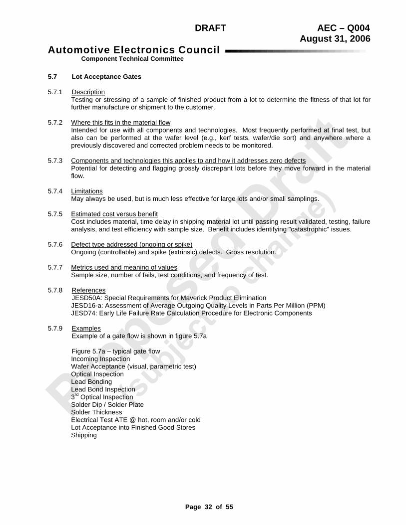
JESD50A: Special Requirements for Maverick Product Elimination JESD16-a: Assessment of Average Outgoing Quality Levels in Parts Per Million (PPM) JESD74: Early Life Failure Rate Calculation Procedure for Electronic Components 5.7.9 Examples Example of a gate flow is shown in figure 5.7a Figure 5.7a – typical gate flow
Incoming Inspection Wafer Acceptance (visual, parametric test) Optical Inspection Lead Bonding Lead Bond Inspection 3rd Optical Inspection Solder Dip / Solder Plate Solder Thickness Electrical Test ATE @ hot, room and/or cold Lot Acceptance into Finished Good Stores Shipping

DRAFT AEC – Q004
August 31, 2006
Component Technical CommitteeAutomotive Electronics Council
Page 33 of 55
6. CAPABILITY 6.1 Stress-Strength Analysis 6.1.1 Description
The analysis of the likelihood of failure based on the probability of stress exceeding the probability of strength for a given part.
6.1.2 Where this fits in the material flow Used for all components and technologies during the testing phase. Can also be modeled in the
design phase if enough information is available. 6.1.3 Components and technologies this applies to and how it addresses zero defects Determines the amount of design or process margin for a given application to indicate the potential
likelihood of failure. 6.1.4 Limitations Usually not needed for industry standard commodity parts or mature device types. 6.1.5 Estimated cost versus benefit Cost includes testing and data analysis, material costs, and statistical software. Benefit includes
design margin analysis and robustness validation. 6.1.6 Defect type addressed (ongoing or spike) Ongoing (controllable) defects. 6.1.7 Metrics used and meaning of values Design margin, TCE, and mean/standard deviation of stress versus strength. 6.1.8 References
6.1.9 Examples Example of a stress-strength contour plot is shown in figure 6.1a
Figure 6.1a – Contour plot of stress vs strength (Reference: http://www.weibull.com)

DRAFT AEC – Q004
August 31, 2006
Component Technical CommitteeAutomotive Electronics Council
Page 34 of 55
6.2 Data Analysis 6.2.1 Description
Mathematical and graphical representations of part population failure distributions over time or stress. 6.2.2 Where this fits in the material flow Intended for use with all components and technologies, anywhere where you have data that needs to
be analyzed to draw conclusions. 6.2.3 Components and technologies this applies to and how it addresses zero defects Quantitative evaluation of an experiment or manufacturing process that gives an indication of actual
or potential failure rates. 6.2.4 Limitations Always used. 6.2.5 Estimated cost versus benefit Cost includes labor, time, and software development. Benefit includes identifying and correcting
issues through data. 6.2.6 Defect type addressed (ongoing or spike) Ongoing (controllable) and spike (extrinsic) defects. 6.2.7 Metrics used and meaning of values General statistics (e.g., mean, standard deviation, Cpk, failure rate, time-to-failure, etc.). 6.2.8 References
http://www.itl.nist.gov/div898/handbook/index.htm 6.2.9 Examples
A list of different methods of data analysis is shown in figure 6.2a
• Exploratory data analysis • Production process characterization • Measurement process characterization • Process modeling • Process improvement • Process or product monitoring and control • Product and process comparisons • Assessing product reliability • Data mining

DRAFT AEC – Q004
August 31, 2006
Component Technical CommitteeAutomotive Electronics Council
Page 35 of 55
6.3 Industry Standards 6.3.1 Description
Agreements among world leaders in part manufacture and use that set benchmarks for testing of parts to determine fitness for use.
6.3.2 Where this fits in the material flow Standards apply to many locations within the material/process flow and offline. Intended for use with
all wafer fab processes and package technologies. 6.3.3 Components and technologies this applies to and how it addresses zero defects Provides standard methods of testing that is applicable for both suppliers and users and offers
benchmarks of performance that can be applied across many devices, processes and materials. 6.3.4 Limitations Not intended for use when there is a need to overstress (i.e., greater acceleration factor) or
understress (i.e., part is inherently weak). If the device has features not covered by any current industry standard.
6.3.5 Estimated cost versus benefit Cost includes engineering time to develop standard, experience, and materials/labor requirements.
Benefit includes uniform application of testing methods and communication of common knowledge. 6.3.6 Defect type addressed (ongoing or spike) Applies to ongoing defects, spike defects, and defect improvement as applicable. 6.3.7 Metrics used and meaning of values Metrics are as defined in each applicable standard. 6.3.8 References
JEDEC, AEC, AIAG, IEC, SAE 6.3.9 Examples Example of a list of standard setting bodies is shown in figure 6.3a
AEC Automotive Electronics Council http://www.aecouncil.org
AMI2 Advanced Memory International http://www.ami2.org/
ANSI American National Standards Institute http://www.ansi.org/
ASME American Society of Mechanical Engineers http://www.asme.org/
ASQC American Society for Quality Control http://www.enre.umd.edu/
ASTM American Society for Testing and Materials http://www.astm.org/
DSCC Defense Supply Center Columbus http://www.dscccols.com/
Free Mil Standards search engine
EIA Electronics Industries Alliance http://www.eia.org/
JEITA
formerly EIAJ Electronic Industries Association Japan
http://www.jeita.org/
Link to standards:
http://tsc.jeita.or.jp/GlS-01.cfm
ESDA Electrostatic Discharge Association http://www.esda.org/
FSA Fabless Semiconductor Association http://www.fsa.org/
IEC International Electrotechnical Commission http://www.iec.ch/

DRAFT AEC – Q004
August 31, 2006
Component Technical CommitteeAutomotive Electronics Council
Page 36 of 55
IEEE Institute of Electrical and Electronics http://www.ieee.org/
IMAPS International Microelectronics and Packaging Society http://www.imaps.org/
IPC Institute for Interconnetion and Packaging Electronic Circuits http://www.ipc.org/
NEMA National Electrical Manufacturers Associations http://www.nema.org/
NIST National Institute of Standards and Technology http://www.nist.gov/
SEMATECH SEMATECH http://www.sematech.org/
SEMI Semiconductor Equipment and Materials International http://www.semi.org/
SIA Semiconductor Industry Association http://www.semichips.org/
SMEMA Surface Mount Equipment Manufacturers Association http://www.smema.org/
SMTA Surface Mount Technology Association http://www.smta.org/
UL Underwriters Laboratories Inc. http://www.ul.com/
Figure 6.3a – Semiconductor and Electronics Industry Standards organizations (Reference: http://www.jedec.org)

DRAFT AEC – Q004
August 31, 2006
Component Technical CommitteeAutomotive Electronics Council
Page 37 of 55
6.4 Environmental Stress Testing 6.4.1 Description
A uniform collection of methods and tests to ensure that products satisfy all of the long term quality and reliability requirements of both manufacturers and consumers alike. Accelerated tests are used to establish a baseline to assess wearout and defectivity concerns. It also assesses resistance of an individual device to the degrading effects of natural elements and actual conditions that might exist in the field, including physical, mechanical, electrical, and environmental stressing.
6.4.2 Where this fits in the material flow Performed on all new and changed components either as a part of the initial product qualification by
the supplier, for qualifying process changes, or as an extended qualification (i.e., failure mechanism monitoring).
6.4.3 Components and technologies this applies to and how it addresses zero defects Identifies inherent weaknesses in the design, process, or package during qualification of the part. Any
or all of these can be corrected prior to release for customer use. 6.4.4 Limitations After the part has been ramped up to full production (i.e., after initial release of the product). 6.4.5 Estimated cost versus benefit Resolving a potential reliability problem up front, prior to product release, is more cost effective in
terms of manpower and effort, than waiting until after the product is out in the field. Customer returns and failure analyses could be more costly to an organization than a slight delay in the release of a product due to added or more comprehensive testing.
6.4.6 Defect type addressed (ongoing or spike) For design, defects include unusual temperature dependencies, performance irregularities and
marginalities, and functional problems. For process, defects include time/temperature defects, unanticipated infant mortality issues, latent defects, and wearout mechanisms. For packaging, defects include structural integrity, unusual package related anomalies (delamination, popcorn) and sensitivities, and assembly related defects that affect quality and reliability. Gross issues are detectable.
6.4.7 Metrics used and meaning of values Number of fails vs. sample size, stress test parameters (e.g., temperature, voltage, current). Data
can be used to pareto the common failure mechanisms. Can also be used to justify improvements in design, process, and packaging.
6.4.8 References
JEDEC JESD22 Test methods AEC Q100 Qualification Requirement
AEC-Q100: Stress Test Qualification for Integrated Circuits AEC-Q101: Stress Test Qualification for Discrete Semiconductors
JEP150: Stress Test Drive Qualification of and Failure Mechanisms Associated With Assembled Solid State Surface Mount Components JESD94: Application Specific Qualification Using Knowledge Based Test Methodology
6.4.9 Examples Example of a test list versus stimuli is shown in figure 6.4a
DRAFT AEC – Q004
August 31, 2006
Component Technical CommitteeAutomotive Electronics Council
Page 38 of 55
6.5 Part Derating 6.5.1 Description
The practice of using the part in a narrower environmental and/or operating envelope than its manufacturer designated limits. Derating can be employed to achieve various goals. The method of derating may need to be adjusted depending on the goal as well.
6.5.2 Where this fits in the material flow Performed on all components, technologies, and applications. Focus is application design, depending
on many application requirements including reliability, criticality, functional performance needs, etc. 6.5.3 Components and technologies this applies to and how it addresses zero defects This practice has been used to provide greater functionality margin within the manufacturer’s
specifications, and with the assistance of the manufacturer, potentially extend useful life or increase reliability.
6.5.4 Limitations Only intended for use with mature products in a mature application. 6.5.5 Estimated cost versus benefit Need good balance between application design cost and derating limits. While design margin is
desirable, stacking of multiple sources of margin can result in high costs and lost opportunities. 6.5.6 Defect type addressed (ongoing or spike) Ongoing defects. 6.5.7 Metrics used and meaning of values Operating conditions such as temperature, humidity, power consumption, operating voltage, and
output current or fan out. NVM erase and write cycles. 6.5.8 References
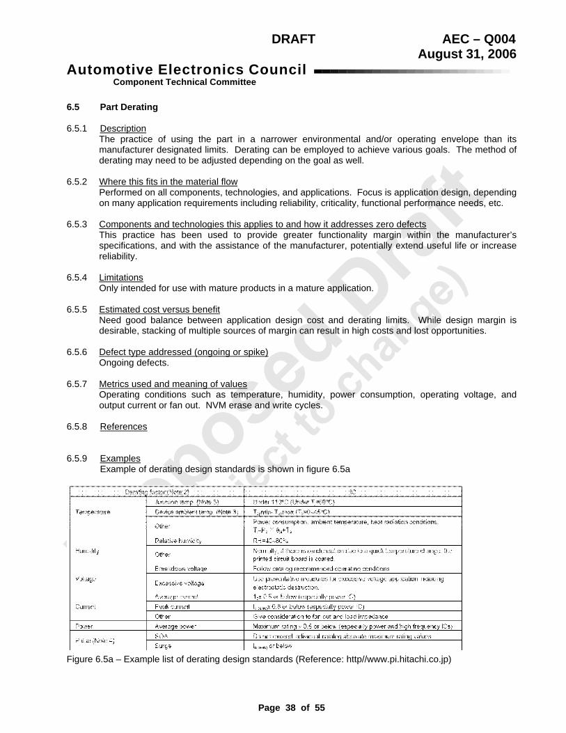
6.5.9 Examples Example of derating design standards is shown in figure 6.5a
Figure 6.5a – Example list of derating design standards (Reference: http//www.pi.hitachi.co.jp)

DRAFT AEC – Q004
August 31, 2006
Component Technical CommitteeAutomotive Electronics Council
Page 39 of 55
7. IMPROVEMENT 7.1 Wafer Level Failure Mechanism Monitoring 7.1.1 Description
The kerf contains a multitude of structures that serve different purposes during wafer production. Among these are structures that are needed for the wafer processing itself (inline), such as lithography alignment structures and structures for measuring layer thicknesses. It also contains structures for physical analysis of the processing, like critical topography structures for construction analysis and fields for measurement of the doping profiles (e.g., by SIMS). Representative structures for electrical analysis of the processing are used for characterization on the wafer. These structures are used, for instance, for measuring sheet resistances and transistor parameters. The kerf also contains special structures for reliability monitoring of the process with fast WLR (wafer level reliability).
7.1.2 Where this fits in the material flow Performed on all major wafer fab process steps and new technologies. The kerf is part of the chip
design and is tested during various points in wafer fabrication. 7.1.3 Components and technologies this applies to and how it addresses zero defects Able to rapidly test for specific failure mechanisms early in manufacture so that faulty wafers or lots
can be fixed or scrapped. 7.1.4 Limitations None. 7.1.5 Estimated cost versus benefit Cost includes designing and testing these monitors, possible loss of wafer space, and rejecting a
wafer. Benefit includes early detection of potential problems, analysis and control of specific fail mechanisms the monitors are designed to address, and providing a statistical basis for analysis and screening.
7.1.6 Defect type addressed (ongoing or spike) Ongoing (controllable) and spike (extrinsic) defects. 7.1.7 Metrics used and meaning of values Kerf or test pattern time to fail or degree of degradation, sample size, frequency of test, and pareto. 7.1.8 References
7.1.9 Examples
Example of a list of failure mechanisms/processes versus wafer level die/kerf tests and packaging test chips is shown in figure 7.1a

DRAFT AEC – Q004
August 31, 2006
Component Technical CommitteeAutomotive Electronics Council
Page 40 of 55
7.2 Process/Product Improvements 7.2.1 Description
Changes to the manufacturing process, component design, materials, construction and testing that improves the product functionality, manufacturability, testability and/or reliability.
7.2.2 Where this fits in the material flow Applies to all components and technologies, anywhere in the flow where agreed major changes are
made (e.g., design, manufacture, test). 7.2.3 Components and technologies this applies to and how it addresses zero defects Change in material or process, either to address a root cause issue or as an evolution of a process or
design, to improve device function, yield and/or reliability. 7.2.4 Limitations Not intended for use with a product that is fully mature or is entering obsoletion. 7.2.5 Estimated cost versus benefit Cost includes implementing the change, validation testing, and user validation. Benefit includes
improved product functionality, quality, cost and/or delivery. 7.2.6 Defect type addressed (ongoing or spike) Ongoing (controllable) and spike (extrinsic) defects. 7.2.7 Metrics used and meaning of values Cost save, cycle time reduction, implementation time, and quality/reliability improvement. 7.2.8 References
JEDEC JESD-46 Customer Notification of Product/Process Changes by Semiconductor Suppliers 7.2.9 Examples Example of a change control requirement is shown in figure 7.2a Design Package Assembly
Major design change Assembly site Lead frame base material Waferfab Plating material
Waferfab site Wire bond method Wafer diameter Mold compound material Diffusion dopant Sealing material Gate oxide material Die attach material Gate oxide thickness Dielectric material Marking method Polysilicon dopant type Marking appearance Metallization material Plating technique Metallization thickness Top protective layer material Mechanical Specification Top protective layer thickness Change in case outline Loosening tolerance(s) Die coating material Packing/Shipping /Labeling Die coating thickness Change in Carrier (reel, tray) dimensions
Drypack requirements Testing Environment maximum storage temperature
Test elimination Electrical Specification Change in ac specification Change in dc specification
Figure 7.2a – List of potential process changes (Reference: JEDEC JESD-46)

DRAFT AEC – Q004
August 31, 2006
Component Technical CommitteeAutomotive Electronics Council
Page 41 of 55
7.3 Production Part Monitoring 7.3.1 Description
Periodic reliability testing of a sample of parts with the purpose of monitoring whether a process excursion occurred to create a defect that could be seen in the field. Verify that the process is in control.
7.3.2 Where this fits in the material flow Post-production test sampling for all components and technologies. 7.3.3 Components and technologies this applies to and how it addresses zero defects Ongoing evaluation of reliability capability in order to fix any issues that can be applied to subsequent
manufactured product. 7.3.4 Limitations Not intended for use when the process and/or part matures. 7.3.5 Estimated cost versus benefit Cost includes material, labor, equipment, overhead, and analyzing failures. Benefit includes feedback
to fix potentially ongoing product/process issues. 7.3.6 Defect type addressed (ongoing or spike) Ongoing (controllable) and spike (extrinsic) defects, gross detectability and generally untimely
defects. 7.3.7 Metrics used and meaning of values Number of fails, sample size, test frequency, and test conditions. 7.3.8 References
JESD659: Failure Mechanism Driven Reliability Monitoring 7.3.9 Examples A typical list of production part (or reliability) monitors is shown in figure 7.3a
Reliability Monitor Test Conditions and Stress Matrix
Tests Condition Sample Size/Duration HTOL (High Temperature
Operating Life) Ta = 125OC
Vdd = Vddmax
2,000pcs/month (each process)
2, 20 hrs HTSL (High Temperature
Storage Life) Ta = 125OC
No bias
2,000pcs/month
72 hrs POC (Pressure Pot & operation Test) = 1 cycle
• PPOT Ta = 127OC
RH = 100%
Pressure = 2.5atm
100pcs/month (each process)
40 hrs
EFR

DRAFT AEC – Q004
August 31, 2006
Component Technical CommitteeAutomotive Electronics Council
Page 42 of 55
• HTOL Ta = 85OC
Vdd = Vddmax
100pcs/month
20 hrs HTOL (High Temperature
Operating Life) Ta = 125OC
Vddmax
100pcs/month (each process)
168, 500, 1,000 hrs
IFR (wafer) HTSL (High Temperature
Storage Life) Ta = 150OC
No bias
100pcs/month (each process)
168, 500, 1,000 hrs TMCL (Temperature Cycle
Test) T (high) = 150OC
T (low) = -65OC
(20 min each temp)
100pcs/month (each process)
100, 300 cycles
PPOT (Pressure Pot Test) Ta = 127OC
RH = 100%
Pressure = 2.5 atm
100pcs/month (each process)
48, 120 hrs
IFR Package
THB (Temperature Humidity w/Bias)
Ta = 85OC
RH = 85%
Vdd = Vddmax
100pcs/month (each process)
168, 500, 1,000 hrs
Figure 7.3a – Typical Reliability Monitor plan (Reference: http://www.hifn.com)

DRAFT AEC – Q004
August 31, 2006
Component Technical CommitteeAutomotive Electronics Council
Page 43 of 55
8. PROBLEM SOLVING 8.1 Design for Analysis 8.1.1 Description
The practice of designing the circuitry such that failure analysis can be performed as efficiently as possible for elimination of no defect found.
8.1.2 Where this fits in the material flow Intended for use with all components with a large number of metal layers or unique interconnection
schemes (e.g., chip-on-chip) and designed into the product. 8.1.3 Components and technologies this applies to and how it addresses zero defects Provides the capability of a more accurate and accessible analysis of failures which otherwise could
be masked by the proliferation of materials and features over the failed site. 8.1.4 Limitations Not intended for use with low complexity parts (few metal levels). 8.1.5 Estimated cost versus benefit Cost includes layout complexity and potential design time increase. Benefit includes ability of easier
and more efficient failure analysis. 8.1.6 Defect type addressed (ongoing or spike) Ongoing (controllable) and spike (extrinsic) defects. 8.1.7 Metrics used and meaning of values Reduced cycle time for FA and reduced incidence of NPF/TNI. 8.1.8 References
8.1.9 Examples Example of a circuit block that is designed for ease of failure analysis is shown in figure 8.1a

DRAFT AEC – Q004
August 31, 2006
Component Technical CommitteeAutomotive Electronics Council
Page 44 of 55
8.2 Problem Solving Techniques 8.2.1 Description
A problem-solving methodology for product and process improvement. It is a team-oriented approach used to identify root cause, contain and correct the problem, verify the problem is understood and solved, and prevent its recurrence. It is also used as a reporting tool to document the issue for a customer.
8.2.2 Where this fits in the material flow This discipline can be used on all components and technologies throughout the manufacturing
process at the supplier, user, or end customer. 8.2.3 Components and technologies this applies to and how it addresses zero defects By identifying and correcting the real root causes, with the results to be applied to similar
devices/processes 8.2.4 Limitations Not intended for use if a failure never occurs. 8.2.5 Estimated cost versus benefit If 8D is well documented this is a very powerful tool that allows to remove problems and to avoid
reoccurrence. Cost includes man-hours in generating document and assembling data. Benefit includes conveying problem resolution and lessons learned to user and supplier.
8.2.6 Defect type addressed (ongoing or spike) Ongoing (controllable) and spike (extrinsic) defects. 8.2.7 Metrics used and meaning of values Cycle time, effectiveness of resolved corrective/preventive action, and field/warranty return rates. 8.2.8 References
JESD671: Component Quality Problem Analysis and Corrective Action Requirements 8.2.9 Examples Example of an Is-Is Not diagram is shown in figure 8.2a, eight discipline list in figure 8.2b
Figure 8.2a – Is-Is Not Diagram (Reference: http://www.quality-one.com)

DRAFT AEC – Q004
August 31, 2006
Component Technical CommitteeAutomotive Electronics Council
Page 45 of 55
8 Disciplines (8D)
DØ – Prepare for the 8D Process
D1 – Establish The Team
D2 – Describe The Problem
D3 – Develop the Interim Containment Action.and Verification. (ICA)
D4 – Define and Verify Root Cause and Escape Point
D5 – Choose and Verify Permanent Corrective Actions (Pcas) for Root Cause and Escape Point
D6 – Implement and Validate Permanent Corrective Actions (PCA)
D7 – Prevent Recurrence
D8 – Recognize Team and Individual Contributions
Figure 8.2b – Eight disciplines for problem solving (Reference: http://www.quality-one.com)

DRAFT AEC – Q004
August 31, 2006
Component Technical CommitteeAutomotive Electronics Council
Page 46 of 55
8.3 Failure Analysis Process 8.3.1 Description
The process of determining the root cause of the failure through testing, observation and physical analysis of the failed component. Testing verifies the failure mode, observation identifies the location of the failure in the component, and physical analysis reveals the failure mechanism.
8.3.2 Where this fits in the material flow Intended for use with all components and technologies, anywhere in the material flow where there is
fallout that requires obtaining more information about the failure. 8.3.3 Components and technologies this applies to and how it addresses zero defects By physically determining the root cause of an issue via device deprocessing and chemical/structural
analysis. 8.3.4 Limitations Not intended for use if a failure never occurs. 8.3.5 Estimated cost versus benefit Cost includes equipment, overhead, labor, and failure (at supplier, at Tier One, at OEM, warranty).
Benefit includes learning about and fixing failure and product improvement. 8.3.6 Defect type addressed (ongoing or spike) Ongoing (controllable) and spike (extrinsic) defects. 8.3.7 Metrics used and meaning of values Cycle time, cost, equipment availability and utilization, and backlog. 8.3.8 References
JESD671: Component Quality Problem Analysis and Corrective Action Requirements 8.3.9 Examples Example of a failure analysis flow and capability is shown in figure 8.3a

DRAFT AEC – Q004
August 31, 2006
Component Technical CommitteeAutomotive Electronics Council
Page 47 of 55
Solicit additional data
Time, voltage, temp,symptoms, process,
(Consider JEP134 format)
Research
Conditions, Part numbers,Trends, Safety impact, etc.
Receive suspectfailed component
Non-Destruct Analysis
Visual, Circuit Analysis,Electricals, X-ray, Curve
tracer, etc.
Re-create failure
Thermal, storage, shock,burn-in, humidity, etc.
Classify failure mode
Parameteric, Open, Short,Functional, etc.
Issue final report
Root cause
Corrective action
Determine preventionand measure(s)
Confirmfailure?
Analysis Planning
Monitor
Issue PreliminaryReport
Destruct Analysis
De-cap, SEM, EDS, Auger,Etching, FIB, Cross-section,
De-process, etc.
AdequateInfo?
Confirmfailure?
NO
YES
NO
NO
YES
YES
Figure 8.3a – Failure Analysis flow

DRAFT AEC – Q004
August 31, 2006
Component Technical CommitteeAutomotive Electronics Council
Page 48 of 55
8.4 Fault Tree Analysis 8.4.1 Description
Fault tree analysis is a logical, structured process that can help identify potential causes of system failure before the failures actually occur. Fault trees are powerful design tools that can help ensure that product performance objectives are met. Can help to ensure that root cause is identified.
8.4.2 Where this fits in the material flow Intended for use with all components and technologies, after a problem or issue occurs or anywhere
that potential root cause can be identified (design, manufacture). 8.4.3 Components and technologies this applies to and how it addresses zero defects Details all the potential causes of a given failure mode in order to investigate and eliminate each
possible root cause until the correct one is found. 8.4.4 Limitations Not intended for use if a failure never occurs. 8.4.5 Estimated cost versus benefit Cost includes labor and time in generating FTA, analysis time and experimentation costs. Benefit
includes more rapid identification of potential root cause of failure and precursor to FMEA. 8.4.6 Defect type addressed (ongoing or spike) Ongoing (controllable) and spike (extrinsic) defects. 8.4.7 Metrics used and meaning of values Failure modes and mechanisms. 8.4.8 References
The Institution of Electrical Engineers (http://www.iee.org) 8.4.9 Examples Example of a fault tree is shown in figure 8.4a, cause and effect diagram in figure 8.4b
Figure 8.4a – Fault Tree Example (Reference: http://www.iee.org)

DRAFT AEC – Q004
August 31, 2006
Component Technical CommitteeAutomotive Electronics Council
Page 49 of 55
Figure 8.4b – Cause and Effect Diagram (fault tree variant) (Reference: http://www.quality-one.com)

DRAFT AEC – Q004
August 31, 2006
Component Technical CommitteeAutomotive Electronics Council
Page 50 of 55
9. APPLICATION 9.1 System Engineering 9.1.1 Description
Alignment of the system design with the user application through co-engineering activities between supplier and user.
9.1.2 Where this fits in the material flow Intended for use with Microprocessors, crystals and oscillator circuits, regulator/power supply circuits,
power drivers, RF circuits, select memory technologies, etc. Performed as part of supplier selection, technology (die and package) selection, specification definition, development design phase, and design validation iterations.
9.1.3 Components and technologies this applies to and how it addresses zero defects Design related issues could be addressed if the Supplier and user is involved and understands the
use application and requirements. Also, both design teams can become educated on proper device usage and specification.
9.1.4 Limitations Usually not needed for industry standard commodity parts or mature device types. 9.1.5 Estimated cost versus benefit Cost includes Engineering resources, both user and supplier, that are needed early in development
cycle. Benefit includes Validation testing more likely to be successful on first pass and more likely to meet launch release deadlines.
9.1.6 Defect type addressed (ongoing or spike) Ongoing (controllable) defects, inadequate design margin, improper design of the IC, and improper
use of the IC in a given application. 9.1.7 Metrics used and meaning of values Six sigma/statistical design tolerance, product development cycle time, and post mortem. 9.1.8 References
9.1.9 Examples Diagram of component capability versus system use environment is shown in figure 9.1a
Figure 9.1a – Component schmoo relationship to system
SYSTEMF(V,T)
COMPONENTA
COMPONENTB
COMPONENTC
COMPONENTn
V
T
V
T
V
T
V
T
A B
C
n
V
T
F

DRAFT AEC – Q004
August 31, 2006
Component Technical CommitteeAutomotive Electronics Council
Page 51 of 55
9.2 Quality Function Deployment 9.2.1 Description
A structured approach to defining customer needs or requirements and translating them into specific plans to produce products to meet those needs. This understanding of the customer needs is then summarized in a product planning matrix or "house of quality". These matrices are used to translate higher level "what's" or needs into lower level "how's" - product requirements or technical characteristics to satisfy these needs. The use of QFD increases quality by flowing down the customer requirements to the component design, filtering and communicating the important product development data, guiding benchmarking efforts, guiding the allocation of design resources, and aiding in the budgeting of final product costs among the various components.
9.2.2 Where this fits in the material flow Intended for use with all components and systems (e.g., technology development planning, software
development, costing case study, etc.). Used early in the design process based on market application research of potential customers or communication with a specific targeted customer.
9.2.3 Components and technologies this applies to and how it addresses zero defects Minimizes the chances for design errors based on insufficient requirements capturing between the
user and supplier, which can propagate into quality or field failures in the application if not picked up during development.
a. Use the method to save development time that will hopefully reduce costs and allow faster
response to changes in the market. b. Focus the resources on providing those capabilities that drive customer satisfaction. c. Improve communications so that issues that are critical to the success of the product do not get
dropped by mistake. d. The end result will be products which better satisfy the customer and therefore will be much more
popular in the marketplace. 9.2.4 Limitation Not intended for use with a product that is fully mature or is approaching its end of life. 9.2.5 Estimated cost versus benefit Cost includes man-hours in completing the interrelationship matrix documenting and analyzing the
data, from technical requirement and customer requirement. Benefit includes gaining tremendously useful insights and improved new product and process designs.
9.2.6 Defect type addressed (ongoing or spike) Addresses more of an ongoing defect or “predictable” issues. 9.2.7 Metrics used and meaning of values The “House of Quality" matrix is the most recognized form of QFD. It translates customer
requirements, drawing upon market research and benchmarking data, into an appropriate number of prioritized engineering targets to be met by a new product design. The general format of the "House of Quality" is made up of six major components that are completed in the course of a QFD project:
a. Customer Requirements (HOWs): A structured list of requirements derived from customer
statements. b. Technical Requirements (WHATs): A structured set of relevant and measurable product
characteristics. c. Planning Matrix: Illustrates customer perceptions observed in market surveys. Includes relative
importance of customer requirements, company and competitor performance in meeting these requirements.
d. Interrelationship Matrix: Illustrates the QFD team's perceptions of interrelationships between technical and customer requirements. An appropriate scale is applied, illustrated using symbols

DRAFT AEC – Q004
August 31, 2006
Component Technical CommitteeAutomotive Electronics Council
Page 52 of 55
or figures. Filling this portion of the matrix involves discussions and consensus building within the team and can be time consuming. Concentrating on key relationships and minimizing the numbers of requirements are useful techniques to reduce the demands on resources.
e. Technical Correlation (Roof) Matrix: Used to identify where technical requirements support or impede each other in the product design. Can highlight innovation opportunities.
f. Technical Priorities, Benchmarks, and Targets: Used to record the priorities assigned to technical requirements by the matrix, measures of technical performance achieved by competitive products and the degree of difficulty involved in developing each requirement. The final output of the matrix is a set of target values for each technical requirement to be met by the new design, which are linked back to the demands of the customer
9.2.8 References
“QFD – The Customer Driven Approach to Quality Planning and Deployment”, edited by Shigeru Mizuno and Yoji Akao, originators of the technique (1993, Asian Productivity Organization).
9.2.9 Examples Example of a house of quality diagram is shown in figure 9.2a
Figure 9.2a - House of Quality example (Reference: www.isixisgma.com)
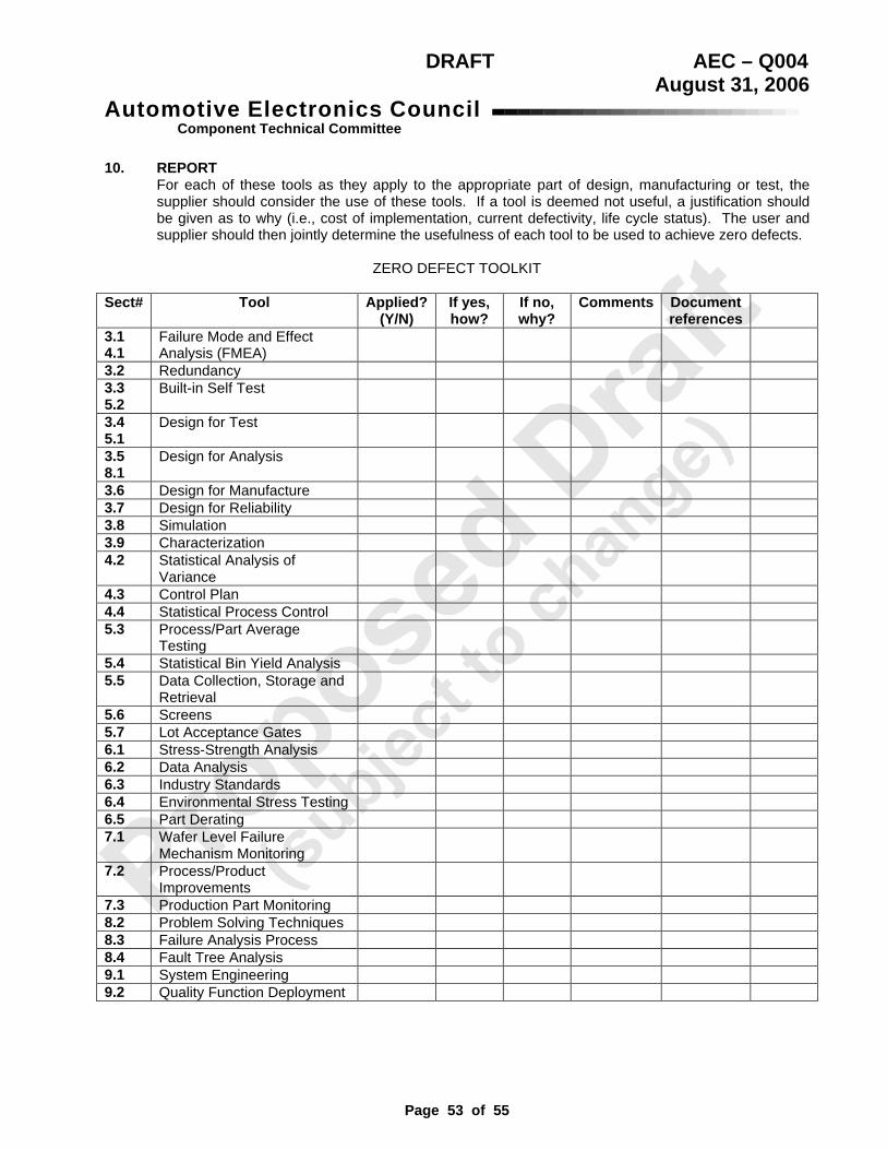
DRAFT AEC – Q004
August 31, 2006
Component Technical CommitteeAutomotive Electronics Council
Page 53 of 55
10. REPORT For each of these tools as they apply to the appropriate part of design, manufacturing or test, the supplier should consider the use of these tools. If a tool is deemed not useful, a justification should be given as to why (i.e., cost of implementation, current defectivity, life cycle status). The user and supplier should then jointly determine the usefulness of each tool to be used to achieve zero defects.
ZERO DEFECT TOOLKIT
Sect# Tool Applied?
(Y/N) If yes, how?
If no, why?
Comments Document references
3.1 4.1
Failure Mode and Effect Analysis (FMEA)
3.2 Redundancy
3.3 5.2
Built-in Self Test
3.4 5.1
Design for Test
3.5 8.1
Design for Analysis
3.6 Design for Manufacture
3.7 Design for Reliability
3.8 Simulation
3.9 Characterization
4.2 Statistical Analysis of Variance
4.3 Control Plan
4.4 Statistical Process Control
5.3 Process/Part Average Testing
5.4 Statistical Bin Yield Analysis
5.5 Data Collection, Storage and Retrieval
5.6 Screens
5.7 Lot Acceptance Gates
6.1 Stress-Strength Analysis
6.2 Data Analysis
6.3 Industry Standards
6.4 Environmental Stress Testing
6.5 Part Derating
7.1 Wafer Level Failure Mechanism Monitoring
7.2 Process/Product Improvements
7.3 Production Part Monitoring
8.2 Problem Solving Techniques
8.3 Failure Analysis Process
8.4 Fault Tree Analysis
9.1 System Engineering
9.2 Quality Function Deployment

DRAFT AEC – Q004
August 31, 2006
Component Technical CommitteeAutomotive Electronics Council
Page 54 of 55
Revision History
Rev # -
Date of change
August 31, 2006
Brief summary listing affected sections Proposed DRAFT document published for 6-month industry review period, scheduled to expire on April 1, 2007.