zl2105ev2 user guide - renesas electronics
TRANSCRIPT

Description The ZL2105 is an innovative mixed-signal power management and conversion IC that combines an integrated step-down DC-DC converter with key power and thermal management functions in a single package. The ZL2105EV2 platform allows evaluation of the features in the highly configurable ZL2105 in either stand-alone mode or via an I2C/SMBus interface.
A USB-to-SMBus adapter board can be used to connect the ZL2105EV2 board to a PC. The PMBus command set is accessed by using the Zilker Labs PowerNavigator™ evaluation software from a PC running Microsoft Windows.
Features • Small, compact design• PMBus control• Pin-strap selection for stand-alone operation• VOUT settable from +0.6 V to +5 V• Convenient power connection• Onboard enable switch• Power good indicator
Target Specifications This board has been designed as a buck regulator for the following conditions: • VIN = 12 V (Board range 4.5 V to 14 V)• VOUT = 3.3 V (Board range 0 to 5 V)• IMAX = 3 A (Board range 0 to 3 A)• fsw = 400 kHz• Efficiency: 83% peak• Output ripple: 0.5%• Dynamic response: 3% (1–2A step, di/dt=2.5A/µs)• Temperature: 25°C
ZL2105
PG
SYNC
EN
POWER IN
POWER OUTSW1
J12 J13
SMBusSYNCSMBus
3
VTRK
Track Input Track Output
Figure 1. ZL2105EV2 Block Diagram
User ManualAN1467
REV.0.00 May 07, 2009
ZL2105EV2Evaluation Board (Rev 1)
Page 1 of 18AN1467 Rev.0.00
May 07, 2009

Functional Description The ZL2105EV2 provides all circuitry required to demonstrate the features of the ZL2105. The ZL2105EV2 has a functionally-optimized ZL2105 circuit layout that allows efficient operation up to the maximum output current. Power and load connections are provided through plug-in sockets.
Stand alone operation is achieved using the pin-strap settings for the device. The pin-strap settings are described in the ZL2105 data sheet [1].
The ZL2105 Evaluation Board is shown in Figure 2. The SMBus address is selectable through jumpers on the top side of the board. All power to the board (VIN and I2C bus) must be removed before changing the jumpers. The back side of the board has 0402 resistor footprints for setting the application pins using resistors.
The hardware enable function is controlled by a toggle switch on the ZL2105EV2 board. The power good (PG) LED is powered from the SMBus/I2C source; it indicates the correct state of PG when external power is applied to the ZL2105EV2 board. The right angle headers at opposite ends of the board are for connecting a USB to I2C control board or for daisy chaining of multiple evaluation boards.
Figure 3 shows the ZL2105 operational circuit. The circuit consists of the ZL2105 power conversion and management IC with its minimal component count to realize a buck converter. The board layout has been optimized for thermal performance. For thermal design considerations relating to the ZL2105, refer to Zilker Labs application note AN10[2].
Figure 5 on Page 8 illustrates the input and output power connections for the ZL2105. The optional input capacitors and output capacitors are also shown on this page.
Operation
Stand Alone Operation The ZL2105 is easy to setup and operate. It is configured, out of the box, to provide 3.3 V at 3 A from a 12 V source. All input and output connections should to be made before turning the input supply on.
When the input power supply is turned on, the ZL2105 will output the configured voltage and the load applied to VOUT+/VOUT- can be varied.
To modify the pin-strap setting of the ZL2105, input power must be turned off. The user pin-strap resistor pads are on the bottom side of the ZL2105EV2 PCB. Once the desired pin-strap settings and component changes have been applied, power can be turned on and the output can be evaluated for the newly configured mode. Refer to the ZL2105 data sheet [1] for pin-strap and resistor setting information. Refer to Figure 2 for resistor pad locations.
PMBus Operation The ZL2105 utilizes the PMBus protocol. The PMBus functionality can be controlled via USB from a PC running the Zilker Labs evaluation software in a Windows XP or Windows 2000/NT operating system.
Install the PowerNavigator software using the CD included in the ZL2105EV2 kit or download it from the web at www.zilkerlabs.com.
For PMBus operation, connect another Zilker Labs evaluation board such as the ZL2005EV1 or the USB-to-SMBus adapter board to J12 of the ZL2105EV2 board. When using multiple evaluation boards together, verify that each device is assigned a different SMBus address. Connect the desired load and an appropriate power supply to the input. Place the ENABLE switch in “DISABLE” and turn on the power.
The evaluation software allows modification of all ZL2105 PMBus parameters. Manually configure the ZL2105 through the various
Page 2 of 18AN1467 Rev.0.00
May 07, 2009
ZL2105EV2

screens or load a predefined scenario from a configuration file.
Use the mouse-over pop-ups for help with PowerNavigator. Refer to Zilker Labs application note AN13 [3] for PMBus details.
The ENABLE switch can then be moved to “ENABLE” and the ZL2105 can be tested. Alternately, the PMBus ON-OFF CONFIG and OPERATION commands may be used.
Loop Compensation Settings By default, the ZL2105 EVB is configured for 12 V to 3.3 V conversion at 3 A. The output voltage can be changed by using the V1 and V0 resistor pads or through the use of PMBus commands. If the output voltage is set to 1V or below, the loop compensation needs to be modified. Table 1 summarizes the PID settings. This is achieved by using PMBus commands or by modifying the PowerPlan configuration file.
Table 1. PID Settings versus Output Voltage VOUT Range PID Setting
1V < VOUT ≤ 5.0V A=5000, B=-9016, C=4170
VOUT ≤1V A=10000, B=-18101, C=8324
These settings are included in the configuration file that is stored on the ZL2105 EVB and is shown here and at the end of this data sheet for reference.
For output voltages greater than 1V, the loop compensation is set as: #Loop compensation for 12v:3.3v,
PID_TAPS A=5000, B=-9016, C=4170
#NLR_CONFIG Enable,1.5%,No Outer,1.5%,3,3,0
NLR_CONFIG 0xA250
When the output voltage is set to 1V or less, the loop compensation should be: #Loop compensation for 12V:0.8V
PID_TAPS A=10000, B=-18101, C=8324
#NLR_CONFIG Enable,1.5%,No Outer,2%,3,3,0
NLR_CONFIG 0xA350
Page 3 of 18AN1467 Rev.0.00
May 07, 2009
ZL2105EV2

Quick Start Guide
Stand Alone Operation 1. Set ENABLE switch to “DISABLE”
2. Apply load to VOUT+/VOUT-
3. Connect power supply to VIN+/VIN-(supply turned off)
4. Turn power supply on
5. Set ENABLE switch to “ENABLE”
6. Test ZL2105 operation
7. To change hardware settings, turn inputpower supply OFF, modify resistor settingsand then turn the input power supply ON
USB (PMBus) Operation 1. Follow step 1 - 4 above
2. Insert the Zilker Labs Eval Kit CD
3. Connect USB-to-SMBus adapter board toJ12 of ZL2105EV2
4. Connect supplied USB cable from computerto USB-to-SMBus adapter board
a. Upon first-time connection, the FoundNew Hardware Wizard will appear.
b. Windows XP users: Select ‘No’ atprompt to search the Internet fordrivers.
c. Follow the steps on the screen to installthe drivers from the CD.
5. Install the PowerNavigator evaluationsoftware by running setup.exe from thePowerNavigator_installer folder on the CD.
6. Set voltage to desired value in GUI.
7. Set ENABLE switch on EVB to “ENABLE”
8. Monitor and configure EVB using PMBuscommands in the evaluation software
9. Test the ZL2105 operation using theevaluation software.
Page 4 of 18AN1467 Rev.0.00
May 07, 2009
ZL2105EV2

SMBus Address Jumper settings
Pin-strap resistor settings
Figure 2. ZL2105EV2 Evaluation Board (Top Side and Bottom Side)
Page 5 of 18AN1467 Rev.0.00
May 07, 2009
ZL2105EV2

Schematics
Figure 3. ZL2105EV2 Circuit
Page 6 of 18AN1467 Rev.0.00
May 07, 2009
ZL2105EV2

Figure 4. ZL2105EV2 Interface
Page 7 of 18AN1467 Rev.0.00
May 07, 2009
ZL2105EV2
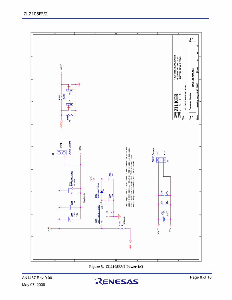
Figure 5. ZL2105EV2 Power I/O
Page 8 of 18AN1467 Rev.0.00
May 07, 2009
ZL2105EV2
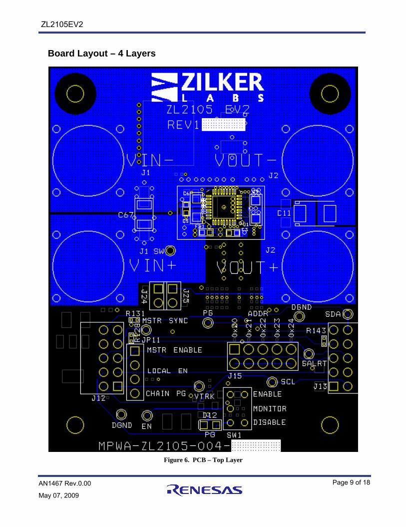
Board Layout – 4 Layers
Figure 6. PCB – Top Layer
Page 9 of 18AN1467 Rev.0.00
May 07, 2009
ZL2105EV2

Figure 7. PCB – Inner Layer 1 (Viewed from Top)
Page 10 of 18AN1467 Rev.0.00
May 07, 2009
ZL2105EV2

Figure 8. PCB – Inner Layer 2 (Viewed from Top)
Page 11 of 18AN1467 Rev.0.00
May 07, 2009
ZL2105EV2

Figure 9. PCB – Bottom Layer (Viewed from Top)
Page 12 of 18AN1467 Rev.0.00
May 07, 2009
ZL2105EV2

Typical Performance Data for Buck Regulator Unless noted: Vin = 12V, Vout = 3.3V, fSW = 400kHz, TA = +25°C
70
75
80
85
90
95
0 0.5 1 1.5 2 2.5 3 3.5
Output Current (A)
Effic
ienc
y (%
)
VIN=5V
VIN=12V
VOUT=3.3VfSW=400kHz
Figure 10. Measured Efficiency
Figure 11. Ripple
Page 13 of 18AN1467 Rev.0.00
May 07, 2009
ZL2105EV2

Figure 12. Dynamic Response (1 – 2A load step, di/dt=1A/µs)
Figure 13. Dynamic Response (2 - 1A load step, di/dt=1A/µs)
Page 14 of 18AN1467 Rev.0.00
May 07, 2009
ZL2105EV2
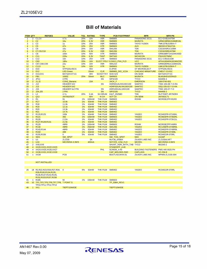
Bill of Materials ITEM QTY REFDES VALUE TOL RATING TYPE PCB FOOTPRINT MFR MFR PN
1 2 C1,C4 4.7u 20% 10V X5R SM0805 PANASONIC-ECG ECJ-GVB1A475M2 1 C2 10u 20% 6.3V X5R SM0805 MURATA GRM21BR60J106ME19L3 1 C3 1u 10% 25V X5R SM0603 TAIYO YUDEN TMK107BJ105KA-T4 1 C5 47n 10% 25V X7R SM0603 AVX 06033C473KAT2A5 1 C6 10u 20% 16V X5R SM1206 TDK C3216X5R1C106M6 3 C7,C9,C10 47u 20% 6.3V X5R SM1206 TDK C3216X5R0J476M7 1 C8 100n 10% 50V X7R SM0603 MURATA GRM188R71H104KA93D8 1 C11 220u 20% 6.3V TANT SM7343 NICHICON F910J227MNC9 1 C12 10n 10% 25V X7R SM0603 PANASONIC-ECG ECJ-1VB1E103K
10 1 C63 180u 20% 16V ELECT POLY 8.3X8.3_PXA_FLD UCC APXA160ARA181MHC0G11 3 C67,C68,C69 22u 10% 16V X5R SM1210 MURATA GRM32ER61C226KE20L12 1 C113 1u 10% 10V X7R SM0603 TAIYO YUDEN LMK107BJ105KA-T13 1 D10 STPS20L45CG 45V D-2PAK ST MICROELECT STPS20L45CG14 1 D12 LED Green 20mA CLR SM0805_DIO_1C2A CHICAGO MINIATURE CMD17-21VGC15 2 D13,D15 BAT54XV2T1G 30V SCHOTTKY SOD-523 ON SEMI BAT54XV2T1G16 1 FB1 1000Z 25% 50mA MLC SM0603 MURATA BLM18HD102SN1D17 1 JP11 4 PIN SN SIP4/100 TYCO 644456-418 2 J1,J2 CON2_Banana 15A JACK_F EMERSON 108-0740-00119 1 J12 HEADER 5X2 SN HDR5DUALRA100X100 SAMTEC TSW-105-08-T-D-RA20 1 J13 HEADER 5X2 HDRF5DUALRA100X100 SAMTEC SSQ-105-02-T-D-RA21 1 J15 HEADER 5x2 PIN SN HDR10DUAL100X100 SAMTEC TSW-105-07-T-D22 2 J24,J25 2 PIN SN SIP2/100 TYCO 644456-223 1 L2 4.7u 20% 3.4A SH DRUM IHLP_2525BD TDK RLF7030T-4R7M3R424 1 Q12 2N7002/SOT 60V N-CH SOT-23 ON SEMI 2N7002LT125 1 R1 91 1% 100mW THK FILM SM0603 ROHM MCR03EZPFX91R027 1 R17 10.0k 1% 63mW THK FILM SM040228 1 R18 11.0k 1% 63mW THK FILM SM040229 1 R19 12.1k 1% 63mW THK FILM SM040230 1 R20 13.3k 1% 63mW THK FILM SM040231 1 R21 14.7k 1% 63mW THK FILM SM040232 2 R120,R125 100k 1% 63mW THK FILM SM0402 YAGEO RC0402FR-07100KL33 1 R121 392 1% 100mW THK FILM SM0603 YAGEO RC0603FR-07392RL34 1 R126 2.21k 1% 63mW THK FILM SM0402 YAGEO RC0402FR-072K21L35 3 R127,R128,R131 21.5k 1% 63mW THK FILM SM040236 1 R129 49R9 1% 100mW THK FILM SM0603 ROHM MCR03EZPFX49R937 1 R130 49R9 1% 250mW THK FILM SM1206 YAGEO RC1206FR-0749R9L38 2 R143,R144 49R9 1% 63mW THK FILM SM0402 YAGEO RC0402FR-0749R9L39 1 R150 499 1% 63mW THK FILM SM0402 YAGEO RC0402FR-07499L40 2 R155,R156 0 5% 63mW THK FILM SM0402 YAGEO RC0402JR-070RL42 1 SW1 SW_SPDT SW_TOG_SPDT NKK G13AP44 1 U1 ZL2105 3A MLF36_6X6BX ZILKER LABS INC ZL2105ALNFT45 1 U10 MIC2920A-3.3WS 400mA SOT223_1234_FLD MICREL MIC2920A-3.3WS47 2 XX8,XX9 SHUNT_HDR_WITH_TAB TYCO 881545-248 4 XX20,XX21,XX22,XX23 STANDOFF_4-4049 4 XX24,XX25,XX26,XX27 PHL SCREW_4-40 BUILDING FASTENERS PMS 440 0025 PH50 4 XX30,XX31,XX32,XX33 CAP_MOLDED.25ID CAPLUGS VC-234-851 1 XX34 PCB BDOTLN3.0HX4.0L ZILKER LABS INC MPWB-ZL2105-004
NOT INSTALLED:
26 18 R2,R22,R23,R26,R27,R34, 0 5% 63mW THK FILM SM0402 YAGEO RC0402JR-070RLR35,R100,R134,R135,R136,R137,R142,R145,R152,R153,R157,R158
41 1 R185 NI 1% 100mW THK FILM SM060343 10 TP1,TP2,TP5,TP6,TP7,TP8, T POINT S TP_036H_REV1
TP10,TP11,TP12,TP1346 1 XX1 TIEPT/10WIDE TIEPT/10WIDE
Page 15 of 18AN1467 Rev.0.00
May 07, 2009
ZL2105EV2

Default Configuration Text
The following text is loaded into the ZL2105EV2 as default settings. Each PMBus command is loaded via the ZL2105EV2 interface software. The # symbol is used for a comment line.
#ZL2105-002-DB08 #NOTE: This file is intended for the Rev. 1 ZL2105-EV2 with L=4.7uH, Co=3x(47uF/2.5mohm)+(220uF/250mohm)
#Configuration File Format: #PMBus Command <tab> Hex Value
#Erase user store & default store RESTORE_FACTORY STORE_USER_ALL STORE_DEFAULT_ALL
#RESPONSES #low FET not enabled for output OV and UV count to 2 OVUV_CONFIG 0x01
#LIMITS VIN_UV_FAULT_LIMIT 4.5
#Set output peak/valley current protection to 4.0 to -4.0A IOUT_OC_FAULT_LIMIT 4 IOUT_UC_FAULT_LIMIT -4
#Set output average current protection to 3.3 to -3.3A IOUT_AVG_OC_FAULT_LIMIT 3.3IOUT_AVG_UC_FAULT_LIMIT -3.3
#SETTINGS #Set Vout to 3.3V VOUT_COMMAND 3.30000
#Set IOUT_SCALE to 151mOhms IOUT_SCALE 151
#Set IOUT_OFFSET to -0.4A IOUT_CAL_OFFSET -0.4A
#Use Rdson internal current sense method with internal tempco sensor, delay 512nS, 3 counts MFR_CONFIG 0x8100
#Set temperature compensation at 400ppm/ C internal temp sensor TEMPCO_CONFIG 0x04
#Set deadtime to 0ns H-L min dynamic and 16ns L-H fixed DEADTIME_CONFIG 0x0086DEADTIME 0x0010
#Loop compensation for 12v:3.3v, ~100mv peak under 1-2A transient @ 2.5A/us, with NLR. PID_TAPS A=5000, B=-9016, C=4170 #NLR_CONFIG Enable,1.5%,No Outer,1.5%,3,3,0 NLR_CONFIG 0xA250
#Loop compensation for 12V:0.8V, ~20kHz BW, ~60deg PM, ~30mv peak under 0.5A step #PID_TAPS A=10000, B=-18101, C=8324 #NLR_CONFIG Enable,1.5%,No Outer,2%,3,3,0 #NLR_CONFIG 0xA350
STORE_DEFAULT_ALL RESTORE_DEFAULT_ALL
Page 16 of 18AN1467 Rev.0.00
May 07, 2009
ZL2105EV2

References [1] ZL2105 Data Sheet, Zilker Labs, Inc., 2008.
[2] AN10 – ZL2005 and ZL2105 Thermal and Layout Guideline, Zilker Labs, Inc., 2006.
[3] AN13 – PMBus™ Command Set, Zilker Labs, Inc., 2007.
Ordering Information
Orderable Part Number Description
ZL2105EVK2 ZL2105 Evaluation Kit, one channel
ZL2105EV2 ZL2105 Evaluation board only
Revision History
Date Rev. #
1-22-08 1.0 Initial Release based on ZL2105EV1 data sheet
Page 17 of 18AN1467 Rev.0.00
May 07, 2009
ZL2105EV2

http://www.renesas.comRefer to "http://www.renesas.com/" for the latest and detailed information.
Renesas Electronics CorporationTOYOSU FORESIA, 3-2-24 Toyosu, Koto-ku, Tokyo 135-0061, JapanRenesas Electronics America Inc.1001 Murphy Ranch Road, Milpitas, CA 95035, U.S.A.Tel: +1-408-432-8888, Fax: +1-408-434-5351Renesas Electronics Canada Limited9251 Yonge Street, Suite 8309 Richmond Hill, Ontario Canada L4C 9T3Tel: +1-905-237-2004Renesas Electronics Europe LimitedDukes Meadow, Millboard Road, Bourne End, Buckinghamshire, SL8 5FH, U.KTel: +44-1628-651-700Renesas Electronics Europe GmbHArcadiastrasse 10, 40472 Düsseldorf, Germany Tel: +49-211-6503-0, Fax: +49-211-6503-1327Renesas Electronics (China) Co., Ltd.Room 1709 Quantum Plaza, No.27 ZhichunLu, Haidian District, Beijing, 100191 P. R. ChinaTel: +86-10-8235-1155, Fax: +86-10-8235-7679Renesas Electronics (Shanghai) Co., Ltd.Unit 301, Tower A, Central Towers, 555 Langao Road, Putuo District, Shanghai, 200333 P. R. China Tel: +86-21-2226-0888, Fax: +86-21-2226-0999Renesas Electronics Hong Kong LimitedUnit 1601-1611, 16/F., Tower 2, Grand Century Place, 193 Prince Edward Road West, Mongkok, Kowloon, Hong KongTel: +852-2265-6688, Fax: +852 2886-9022Renesas Electronics Taiwan Co., Ltd.13F, No. 363, Fu Shing North Road, Taipei 10543, TaiwanTel: +886-2-8175-9600, Fax: +886 2-8175-9670Renesas Electronics Singapore Pte. Ltd.80 Bendemeer Road, Unit #06-02 Hyflux Innovation Centre, Singapore 339949Tel: +65-6213-0200, Fax: +65-6213-0300Renesas Electronics Malaysia Sdn.Bhd.Unit 1207, Block B, Menara Amcorp, Amcorp Trade Centre, No. 18, Jln Persiaran Barat, 46050 Petaling Jaya, Selangor Darul Ehsan, MalaysiaTel: +60-3-7955-9390, Fax: +60-3-7955-9510Renesas Electronics India Pvt. Ltd.No.777C, 100 Feet Road, HAL 2nd Stage, Indiranagar, Bangalore 560 038, IndiaTel: +91-80-67208700, Fax: +91-80-67208777Renesas Electronics Korea Co., Ltd.17F, KAMCO Yangjae Tower, 262, Gangnam-daero, Gangnam-gu, Seoul, 06265 KoreaTel: +82-2-558-3737, Fax: +82-2-558-5338
SALES OFFICES
© 2018 Renesas Electronics Corporation. All rights reserved.Colophon 7.2
(Rev.4.0-1 November 2017)
Notice1. Descriptions of circuits, software and other related information in this document are provided only to illustrate the operation of semiconductor products and application examples. You are fully responsible for
the incorporation or any other use of the circuits, software, and information in the design of your product or system. Renesas Electronics disclaims any and all liability for any losses and damages incurred by
you or third parties arising from the use of these circuits, software, or information.
2. Renesas Electronics hereby expressly disclaims any warranties against and liability for infringement or any other claims involving patents, copyrights, or other intellectual property rights of third parties, by or
arising from the use of Renesas Electronics products or technical information described in this document, including but not limited to, the product data, drawings, charts, programs, algorithms, and application
examples.
3. No license, express, implied or otherwise, is granted hereby under any patents, copyrights or other intellectual property rights of Renesas Electronics or others.
4. You shall not alter, modify, copy, or reverse engineer any Renesas Electronics product, whether in whole or in part. Renesas Electronics disclaims any and all liability for any losses or damages incurred by
you or third parties arising from such alteration, modification, copying or reverse engineering.
5. Renesas Electronics products are classified according to the following two quality grades: “Standard” and “High Quality”. The intended applications for each Renesas Electronics product depends on the
product’s quality grade, as indicated below.
"Standard": Computers; office equipment; communications equipment; test and measurement equipment; audio and visual equipment; home electronic appliances; machine tools; personal electronic
equipment; industrial robots; etc.
"High Quality": Transportation equipment (automobiles, trains, ships, etc.); traffic control (traffic lights); large-scale communication equipment; key financial terminal systems; safety control equipment; etc.
Unless expressly designated as a high reliability product or a product for harsh environments in a Renesas Electronics data sheet or other Renesas Electronics document, Renesas Electronics products are
not intended or authorized for use in products or systems that may pose a direct threat to human life or bodily injury (artificial life support devices or systems; surgical implantations; etc.), or may cause
serious property damage (space system; undersea repeaters; nuclear power control systems; aircraft control systems; key plant systems; military equipment; etc.). Renesas Electronics disclaims any and all
liability for any damages or losses incurred by you or any third parties arising from the use of any Renesas Electronics product that is inconsistent with any Renesas Electronics data sheet, user’s manual or
other Renesas Electronics document.
6. When using Renesas Electronics products, refer to the latest product information (data sheets, user’s manuals, application notes, “General Notes for Handling and Using Semiconductor Devices” in the
reliability handbook, etc.), and ensure that usage conditions are within the ranges specified by Renesas Electronics with respect to maximum ratings, operating power supply voltage range, heat dissipation
characteristics, installation, etc. Renesas Electronics disclaims any and all liability for any malfunctions, failure or accident arising out of the use of Renesas Electronics products outside of such specified
ranges.
7. Although Renesas Electronics endeavors to improve the quality and reliability of Renesas Electronics products, semiconductor products have specific characteristics, such as the occurrence of failure at a
certain rate and malfunctions under certain use conditions. Unless designated as a high reliability product or a product for harsh environments in a Renesas Electronics data sheet or other Renesas
Electronics document, Renesas Electronics products are not subject to radiation resistance design. You are responsible for implementing safety measures to guard against the possibility of bodily injury, injury
or damage caused by fire, and/or danger to the public in the event of a failure or malfunction of Renesas Electronics products, such as safety design for hardware and software, including but not limited to
redundancy, fire control and malfunction prevention, appropriate treatment for aging degradation or any other appropriate measures. Because the evaluation of microcomputer software alone is very difficult
and impractical, you are responsible for evaluating the safety of the final products or systems manufactured by you.
8. Please contact a Renesas Electronics sales office for details as to environmental matters such as the environmental compatibility of each Renesas Electronics product. You are responsible for carefully and
sufficiently investigating applicable laws and regulations that regulate the inclusion or use of controlled substances, including without limitation, the EU RoHS Directive, and using Renesas Electronics
products in compliance with all these applicable laws and regulations. Renesas Electronics disclaims any and all liability for damages or losses occurring as a result of your noncompliance with applicable
laws and regulations.
9. Renesas Electronics products and technologies shall not be used for or incorporated into any products or systems whose manufacture, use, or sale is prohibited under any applicable domestic or foreign laws
or regulations. You shall comply with any applicable export control laws and regulations promulgated and administered by the governments of any countries asserting jurisdiction over the parties or
transactions.
10. It is the responsibility of the buyer or distributor of Renesas Electronics products, or any other party who distributes, disposes of, or otherwise sells or transfers the product to a third party, to notify such third
party in advance of the contents and conditions set forth in this document.
11. This document shall not be reprinted, reproduced or duplicated in any form, in whole or in part, without prior written consent of Renesas Electronics.
12. Please contact a Renesas Electronics sales office if you have any questions regarding the information contained in this document or Renesas Electronics products.
(Note 1) “Renesas Electronics” as used in this document means Renesas Electronics Corporation and also includes its directly or indirectly controlled subsidiaries.
(Note 2) “Renesas Electronics product(s)” means any product developed or manufactured by or for Renesas Electronics.