zybo z7 reference manual - robotshop...3 usb jtag/uart port 14 user rgb leds * 25 fan connector (5v,...
TRANSCRIPT
2/10/2018 Zybo Z7 Reference Manual [Reference.Digilentinc]
https://reference.digilentinc.com/reference/programmable-logic/zybo-z7/reference-manual 1/33
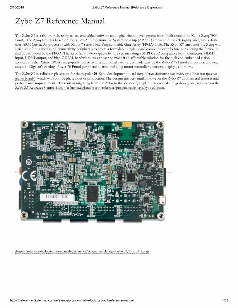
The Zybo Z7 is a feature-rich, ready-to-use embedded software and digital circuit development board built around the Xilinx Zynq-7000family. The Zynq family is based on the Xilinx All Programmable System-on-Chip (AP SoC) architecture, which tightly integrates a dual-core ARM Cortex-A9 processor with Xilinx 7-series Field Programmable Gate Array (FPGA) logic. The Zybo Z7 surrounds the Zynq witha rich set of multimedia and connectivity peripherals to create a formidable single-board computer, even before considering the flexibilityand power added by the FPGA. The Zybo Z7's video-capable feature set, including a MIPI CSI-2 compatible Pcam connector, HDMIinput, HDMI output, and high DDR3L bandwidth, was chosen to make it an affordable solution for the high end embedded visionapplications that Xilinx FPGAs are popular for. Attaching additional hardware is made easy by the Zybo Z7's Pmod connectors, allowingaccess to Digilent's catalog of over 70 Pmod peripheral boards, including motor controllers, sensors, displays, and more.
The Zybo Z7 is a direct replacement for the popular Zybo development board (http://store.digilentinc.com/zybo-zynq-7000-arm-fpga-soc-trainer-board/), which will soon be phased out of production. The designs are very similar, however the Zybo Z7 adds several features andperformance improvements. To assist in migrating from the Zybo to the Zybo Z7, Digilent has created a migration guide, available on theZybo Z7 Resource Center (https://reference.digilentinc.com/reference/programmable-logic/zybo-z7/start).
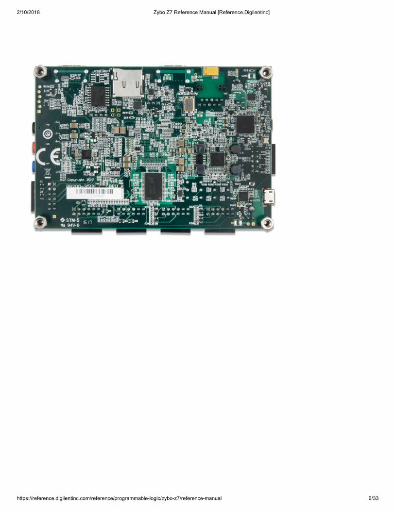
(https://reference.digilentinc.com/_media/reference/programmable-logic/zybo-z7/zybo-z7-5.png)
Zybo Z7 Reference Manual
2/10/2018 Zybo Z7 Reference Manual [Reference.Digilentinc]
https://reference.digilentinc.com/reference/programmable-logic/zybo-z7/reference-manual 2/33
2/10/2018 Zybo Z7 Reference Manual [Reference.Digilentinc]
https://reference.digilentinc.com/reference/programmable-logic/zybo-z7/reference-manual 3/33

2/10/2018 Zybo Z7 Reference Manual [Reference.Digilentinc]
https://reference.digilentinc.com/reference/programmable-logic/zybo-z7/reference-manual 4/33
2/10/2018 Zybo Z7 Reference Manual [Reference.Digilentinc]
https://reference.digilentinc.com/reference/programmable-logic/zybo-z7/reference-manual 5/33
2/10/2018 Zybo Z7 Reference Manual [Reference.Digilentinc]
https://reference.digilentinc.com/reference/programmable-logic/zybo-z7/reference-manual 6/33

2/10/2018 Zybo Z7 Reference Manual [Reference.Digilentinc]
https://reference.digilentinc.com/reference/programmable-logic/zybo-z7/reference-manual 7/33
Zybo Z7 PDF (https://reference.digilentinc.com/_media/reference/programmable-logic/zybo-z7/zybo-z7_rm.pdf)
ZYNQ Processor667 MHz () dual-core Cortex-A9 processorDDR3L memory controller with 8 DMA channels and 4 High Performance AXI3 Slave portsHigh-bandwidth peripheral controllers: 1G Ethernet, USB 2.0, SDIOLow-bandwidth peripheral controllers: SPI, UART, CAN, I2CProgrammable from JTAG, Quad-SPI flash, and microSD cardProgrammable logic equivalent to Artix-7 FPGA
Memory1 GB () DDR3L with 32-bit bus @ 1066 MHz ()16 MB () Quad-SPI Flash with factory programmed 128-bit random number and 48-bit globally unique EUI-48/64™compatible identifiermicroSD slot
PowerPowered from USB or any 5V external power source
USB and EthernetGigabit Ethernet PHYUSB-JTAG Programming circuitryUSB-UART bridgeUSB 2.0 OTG PHY with host and device support
Audio and VideoPcam camera connector with MIPI CSI-2 support
Download This Reference Manual
Features
2/10/2018 Zybo Z7 Reference Manual [Reference.Digilentinc]
https://reference.digilentinc.com/reference/programmable-logic/zybo-z7/reference-manual 8/33
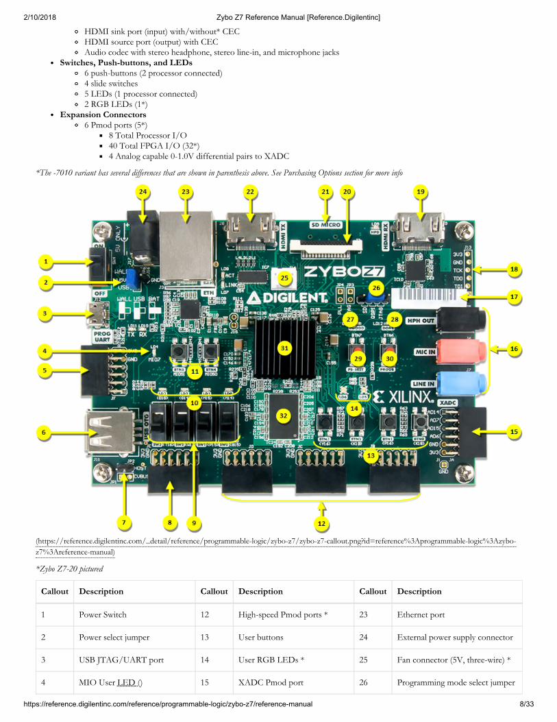
HDMI sink port (input) with/without* CECHDMI source port (output) with CECAudio codec with stereo headphone, stereo line-in, and microphone jacks
Switches, Push-buttons, and LEDs6 push-buttons (2 processor connected)4 slide switches5 LEDs (1 processor connected)2 RGB LEDs (1*)
Expansion Connectors6 Pmod ports (5*)
8 Total Processor I/O40 Total FPGA I/O (32*)4 Analog capable 0-1.0V differential pairs to XADC
*The -7010 variant has several differences that are shown in parenthesis above. See Purchasing Options section for more info
(https://reference.digilentinc.com/_detail/reference/programmable-logic/zybo-z7/zybo-z7-callout.png?id=reference%3Aprogrammable-logic%3Azybo-z7%3Areference-manual)
*Zybo Z7-20 pictured
Callout Description Callout Description Callout Description
1 Power Switch 12 High-speed Pmod ports * 23 Ethernet port
2 Power select jumper 13 User buttons 24 External power supply connector
3 USB JTAG/UART port 14 User RGB LEDs * 25 Fan connector (5V, three-wire) *
4 MIO User LED () 15 XADC Pmod port 26 Programming mode select jumper

2/10/2018 Zybo Z7 Reference Manual [Reference.Digilentinc]
https://reference.digilentinc.com/reference/programmable-logic/zybo-z7/reference-manual 9/33
Callout Description Callout Description Callout Description
5 MIO Pmod port 16 Audio codec ports 27 Power supply good LED ()
6 USB 2.0 Host/OTG port 17 Unique MAC address label 28 FPGA programming done LED ()
7 USB Host power enable jumper 18 External JTAG port 29 Processor reset button
8 Standard Pmod port 19 HDMI input port 30 FPGA clear configuration button
9 User switches 20 Pcam MIPI CSI-2 port 31 Zynq-7000
10 User LEDs 21 microSD connector (other side) 32 DDR3L Memory
11 MIO User buttons 22 HDMI output port * denotes difference between Z7-10 and Z7-20
The Zybo Z7 can be purchased with either a Zynq-7010 or Zynq-7020 loaded. These two Zybo Z7 product variants are referred to as theZybo Z7-10 and Zybo Z7-20, respectively. When Digilent documentation describes functionality that is common to both of these variants,they are referred to collectively as the “Zybo Z7”. When describing something that is only common to a specific variant, the variant will beexplicitly called out by its name.
(https://reference.digilentinc.com/_detail/reference/programmable-logic/zybo-z7/zybo-z7-compare.png?id=reference%3Aprogrammable-logic%3Azybo-z7%3Areference-manual)
The primary difference between the two variants is the size of the FPGA inside the Zynq AP SoC. The Zynq processors both have the samecapabilities, but the -20 has about a 3 times larger internal FPGA than the -10. Also, The Zynq-7010 has slightly fewer FPGA attached pinsthan the Zynq-7020, which means several features found on the Zybo Z7-20 are not available on the Zybo Z7-10. The differences betweenthe two variants are summarized below:
Product Variant Zybo Z7-10 Zybo Z7-20
Zynq Part XC7Z010-1CLG400C XC7Z020-1CLG400C
1 MSPS On-chip ADC () Yes Yes
Look-up Tables (LUTs) 17,600 53,200
Purchasing Options

2/10/2018 Zybo Z7 Reference Manual [Reference.Digilentinc]
https://reference.digilentinc.com/reference/programmable-logic/zybo-z7/reference-manual 10/33
Product Variant Zybo Z7-10 Zybo Z7-20
Flip-Flops 35,200 106,400
Block RAM () 270 KB 630 KB
Clock Management Tiles 2 4
Total Pmod ports 5 6
Fan connector No Yes
Zynq heat sink No Yes
HDMI CEC Support TX port only TX and RX ports
RGB LED () 1 2
The Zybo Z7-20 includes a heat sink in order to dissipate the extra heat generated from the additional FPGA resources when runningcomplex, fast-switching designs.
The board can be purchased stand-alone or with a voucher to unlock the Xilinx SDSoC toolset. The SDSoC voucher unlocks a 1 yearlicense that can be used with the Zybo Z7. After the license expires, any version of SDSoC that was released during this 1 year period cancontinue to be used indefinitely. For more information on purchasing, see the Zybo Z7 Product Page (http://store.digilentinc.com/). At thetime of purchase, it is also possible to add-on a microSD card, 5V 2.5A power supply, and micro USB cable as needed. A small fan thatattaches to the heat sink can be added on to the Zybo Z7-20 too, however this fan will not work with the Zybo Z7-10.
Note that due to the smaller FPGA in the Zynq-7010, it is not very well suited to be used in SDSoC for embedded vision applications. Werecommend people purchase the Zybo Z7-20 if they are interested in these types of applications.
The Zybo Z7 is fully compatible with Xilinx’s high-performance Vivado ® Design Suite. This tool set melds FPGA logic design andembedded ARM software development into an easy to use, intuitive design flow. It can be used for designing systems of any complexity,from a complete operating system running multiple server applications, down to a simple bare-metal program that controls some LEDs. It isalso possible to treat the Zynq AP SoC as a standalone FPGA for those not interested in using the processor in their design. The Zybo Z7 issupported under Vivado's free WebPACK™ license, which means the software is completely free to use, including the Logic Analyzer andHigh-level Synthesis (HLS) features. The Logic Analyzer assists with debugging logic that is running in hardware, and the HLS tool allowsyou to compile C code directly into HDL.
Design resources, example projects, and tutorials are available for download at the Zybo Z7 Resource Center(https://reference.digilentinc.com/reference/programmable-logic/zybo-z7/start).
Zynq platforms are well-suited to be embedded Linux targets, and Zybo Z7 is no exception. Digilent currently does not provide a Petalinuxexample for this product, however one will be available in the near future on the Zybo Z7 Resource Center(https://reference.digilentinc.com/reference/programmable-logic/zybo-z7/start).
The Zybo Z7 can also be used in Xilinx's SDSoC environment, which allows you to design FPGA accelerated programs and video pipelineswith ease in an entirely C/C++ environment. For more information on SDSoC, see the Xilinx SDSoC Site(https://www.xilinx.com/products/design-tools/software-zone/sdsoc.html). Digilent will be releasing a video capable platform with Linux andOpenCV support in the near future. Note that due to the smaller FPGA in the Zybo Z7-10, only very basic video processing demos will beincluded with that platform. Digilent recommends the Zybo Z7-20 for those interested in video processing.
Those familiar with the older Xilinx ISE/EDK toolsets from before Vivado was released can also choose to use the Zybo Z7 in that toolset. Digilent does not provide materials to support this, but you can always ask for help on the Digilent Forum(https://forum.digilentinc.com).
Software Support
Zynq APSoC Architecture

2/10/2018 Zybo Z7 Reference Manual [Reference.Digilentinc]
https://reference.digilentinc.com/reference/programmable-logic/zybo-z7/reference-manual 11/33
The Zynq APSoC is divided into two distinct subsystems: The Processing System (PS) and the Programmable Logic (PL). The figure belowshows an overview of the Zynq APSoC architecture, with the PS colored light green and the PL in yellow. Note that the PCIe Gen2controller and Multi-gigabit transceivers are not available on the Zynq-7020 or Zynq-7010 devices.
(https://reference.digilentinc.com/_detail/zybo/zyng1.png?id=reference%3Aprogrammable-logic%3Azybo-z7%3Areference-manual)
The PL is nearly identical to a Xilinx 7-series Artix FPGA, except that it contains several dedicated ports and buses that tightly couple it tothe PS. The PL also does not contain the same configuration hardware as a typical 7-series FPGA, and it must be configured either directlyby the processor or via the JTAG port.
The PS consists of many components, including the Application Processing Unit (APU, which includes 2 Cortex-A9 processors), AdvancedMicrocontroller Bus Architecture (AMBA) Interconnect, DDR3 Memory controller, and various peripheral controllers with their inputs andoutputs multiplexed to 54 dedicated pins (called Multiplexed I/O, or MIO pins). Peripheral controllers that do not have their inputs andoutputs connected to MIO pins can instead route their I/O through the PL, via the Extended-MIO (EMIO) interface. The peripheralcontrollers are connected to the processors as slaves via the AMBA interconnect, and contain readable/writable control registers that areaddressable in the processors’ memory space. The programmable logic is also connected to the interconnect as a slave, and designs canimplement multiple cores in the FPGA fabric that each also contain addressable control registers. Furthermore, cores implemented in thePL can trigger interrupts to the processors and perform DMA accesses to DDR3 memory.
There are many aspects of the Zynq APSoC architecture that are beyond the scope of this document. For a complete and thoroughdescription, refer to the Zynq Technical Reference manual (http://www.xilinx.com/support/documentation/user_guides/ug585-Zynq-7000-TRM.pdf).
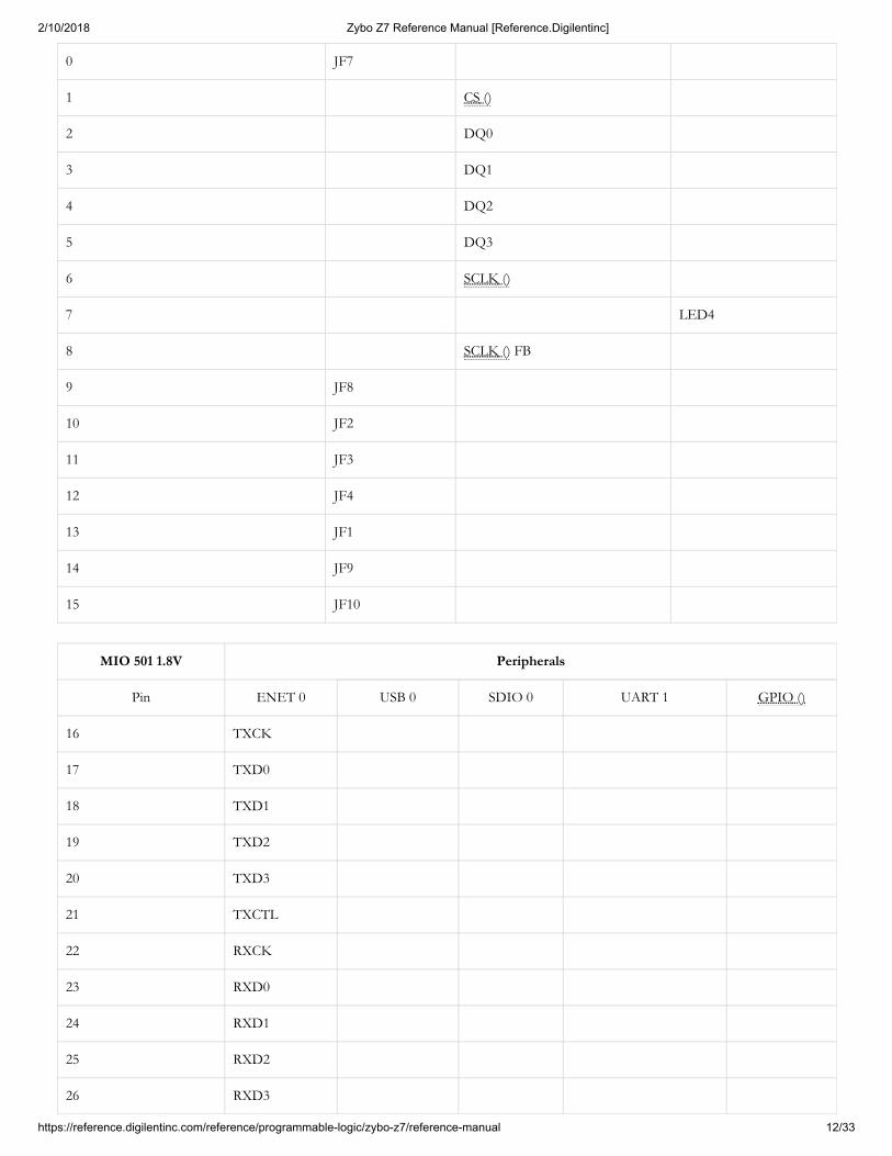
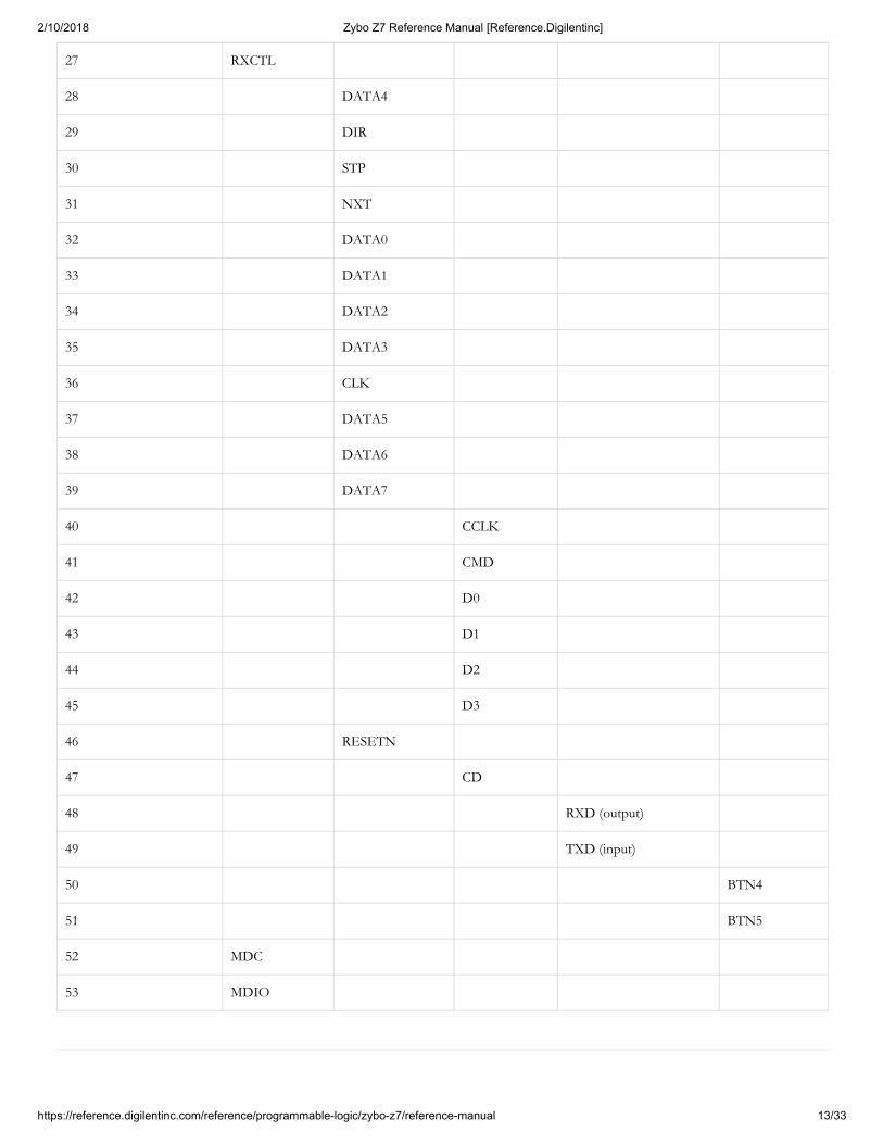
The table below depicts the external components connected to the MIO pins of the Zybo Z7. The Vivado board files found on the ZyboZ7 Resource Center (https://reference.digilentinc.com/reference/programmable-logic/zybo-z7/start) can be used to properly configure the PS towork with these peripherals. It is also possible to use the example projects found on the resource center as a starting point for your owndesigns.
MIO 500 3.3 V Peripherals
Pin Pmod SPI Flash GPIO ()
2/10/2018 Zybo Z7 Reference Manual [Reference.Digilentinc]
https://reference.digilentinc.com/reference/programmable-logic/zybo-z7/reference-manual 12/33
0 JF7
1 CS ()
2 DQ0
3 DQ1
4 DQ2
5 DQ3
6 SCLK ()
7 LED4
8 SCLK () FB
9 JF8
10 JF2
11 JF3
12 JF4
13 JF1
14 JF9
15 JF10
MIO 501 1.8V Peripherals
Pin ENET 0 USB 0 SDIO 0 UART 1 GPIO ()
16 TXCK
17 TXD0
18 TXD1
19 TXD2
20 TXD3
21 TXCTL
22 RXCK
23 RXD0
24 RXD1
25 RXD2
26 RXD3
2/10/2018 Zybo Z7 Reference Manual [Reference.Digilentinc]
https://reference.digilentinc.com/reference/programmable-logic/zybo-z7/reference-manual 13/33
27 RXCTL
28 DATA4
29 DIR
30 STP
31 NXT
32 DATA0
33 DATA1
34 DATA2
35 DATA3
36 CLK
37 DATA5
38 DATA6
39 DATA7
40 CCLK
41 CMD
42 D0
43 D1
44 D2
45 D3
46 RESETN
47 CD
48 RXD (output)
49 TXD (input)
50 BTN4
51 BTN5
52 MDC
53 MDIO

2/10/2018 Zybo Z7 Reference Manual [Reference.Digilentinc]
https://reference.digilentinc.com/reference/programmable-logic/zybo-z7/reference-manual 14/33
The Zybo Z7 power circuitry was carefully designed to meet the requirements of the Zynq-7000 and all other peripherals while alsoproviding flexible input supply options. An overview of the power circuit is shown in Figure 1.1.
(https://reference.digilentinc.com/_detail/reference/programmable-logic/zybo-z7/zybo-z7-power.png?id=reference%3Aprogrammable-logic%3Azybo-z7%3Areference-manual)
Figure 1.1. Power circuit overview
All on-board power supplies are enabled or disabled by the power switch (SW4). The power indicator LED () (LD13, labeled PGOOD) ison when all the supply rails reach their nominal voltage.
The Zybo Z7 can be powered from several different sources. Jumper JP6 (near the power switch) determines which power source is used.There are three valid configurations for this jumper corresponding to the three powering options: USB, wall wart supply with barrel jack,and battery pack. Figure 1.1 depicts all three, and a diagram on the board silkscreen does as well.
The recommended power source is an external power supply (such as a wall-wart) with a barrel jack connector (also known as a coaxialpower connector). The supply must use a center-positive 2.1mm internal-diameter plug and deliver between 4.5V to 5.5V DC. It should alsobe able to output at least 2.5 A (12.5 Watts) in order to support power hungry Zynq projects and external peripherals. To use an externalsupply with a barrel jack, plug it into the power jack (J17), set jumper JP6 to “WALL”, and then set SW4 to “ON”. Suitable supplies can bepurchased from the Digilent website or Digilent distributors, as well as popular electronics vendors.
An external power source, such as a battery pack, that does not have a suitable barrel jack connector can still be used by wiring it’s positiveterminal to the center pin of JP6 and the negative terminal to the pin labeled J16 next to JP6. The external supply must still meet the samevoltage and current requirements as a supply attached to the barrel jack.
It is also possible to power the Zybo Z7 from the USB programming port (J12), however the Zybo Z7 often requires more current than the0.5 A of current that is allowed by a USB 2.0 device. If this limit is exceeded, many USB hosts will begin to droop the voltage briefly untilthe Zybo Z7 resets, dropping current consumption into acceptable ranges. To help prevent this, a USB host port should be chosen that cansupport higher current (often referred to as a “fast charging USB port” or similar by laptop/PC vendors). Many USB battery packs and wallsupplies will also support higher current draws. Even when attached to a host capable of providing more current, the Zybo Z7 will limititself to .75 A, and will reset if this current is reached. If you experience your project resetting (indicated by a brief flicker on the PGOODLED () and the DONE LED () turning off) while powered from a high current USB port, you will either need to lower the powerconsumption of your project or use an external power source.
For reference, we found that the out of box demo loaded on the Zybo Z7 at the factory consumes about 0.5 A from the input powersource. More demanding applications, including any that drive multiple peripheral boards or other USB devices, will likely draw more.
The Zybo Z7 has over-voltage protection up to 20 V on all power inputs that will kick in when a voltage of greater than 5.7 V is detected onthe selected input. It will also limit current draw to .75 A when powered from USB and 4 A when powered from an external source. Thisprotection is implemented using a Texas Instruments TPS25940 eFuse, please refer to its datasheet for further specifications.
Table 1.1.1 provides an overview of the power input specifications for the Zybo Z7.
Functional Description1 Power Supplies
1.1 Power Input Sources

2/10/2018 Zybo Z7 Reference Manual [Reference.Digilentinc]
https://reference.digilentinc.com/reference/programmable-logic/zybo-z7/reference-manual 15/33
ConnectorType
JP6Configuration
ConnectorLabel
Schematic netname
Min/Rec/Max Voltage(V)
Current Limit(A)
Barrel jack WALL J17 VJACK 4.5/5/5.5 4.0
Battery/Other BAT JP6, J16 VU5V0 4.5/5/5.5 4.0
USB USB J12 VBUS See USB specification 0.75
Table 1.1.1. Zybo Z7 Power Input Specifications
Table 1.2.1 describes the characteristics the Zybo Z7's on-board power rails. It can be used to estimate power consumption for a project, ordetermine how much current attached peripherals can draw before being limited.
Net nameUpstream netname
Power ICType
Power ICLabel
Min/Typ/MaxVoltage (V)
Max.Current
Major Devices andConnectors
VCC5V0 VU5V0 Powerprotection
IC26 2.3V/5V/5.7V See Table1.1.1
Power input
VCC3V3 VCC5V0 Buck IC25 3.3V +-10% 1.5A FPGA banks, Ethernet,USB, HDMI
VCC1V0 VCC5V0 Buck IC25 1.0V +-5% 2.1A FPGA, Ethernet
VCC1V35 VCC5V0 Buck IC25 1.35V +-5% 1.2A FPGA, DDR3
VCC1V8 VCC5V0 Buck IC25 1.8V +-10% 0.6A FPGA, Ethernet, USB
XADC_1V8 VCC5V0 LDO IC25 1.8V +-10% 0.1A FPGA XADC
XADC_1V25 VCC3V3 LDO IC27 1.25V +-0.12% 5mA FPGA XADC reference
ANA3V3 VCC5V0 LDO IC5 3.3V +-10% 0.1A Analog audio supply
Table 1.2.1. Zybo Z7 Power Rail Specifications
Input power to the board is gated by the TPS25940, a protection circuit providing both inrush and general current limit, over-voltageprotection and current sense. Inrush current is limited by a ~4ms soft-start time.
The supply rails downstream are daisy-chained to follow the Xilinx-recommended start-up sequence. Flicking the power switch (SW4) willenable the 1.0V rail, which enables the 1.8V digital supply rail, which in turn enables the I/O supply rails 3.3V and 1.35V. The 1.25Vreference and 1.8V analog supply ramp together with the 3.3V rail. Once all the channels of the ADP5052 (IC25) supply reach regulation,the PGOOD signal will assert, enabling the 3.3V audio supply, lighting up the power LED () (LD13), and de-asserting the Power-On Resetsignal (PS_POR_B) of the Zynq.
Each power supply uses a soft-start ramp of 1-10ms to limit in-rush current. There is an additional delay of at least 130ms after the powerrails reach regulation and before the Power-On Reset signal de-assert to allow for the PS_CLK (IC22) to stabilize.
The current being consumed by the Zybo Z7 from the power input can be monitored using the IMON signal of the TPS25940 eFuse device(IC26). The voltage on the IMON signal is directly proportional to the current being consumed, and is connected to the dedicated analoginput pair on the Zynq-7000 (V_P/V_N) so it can be measured using the internal ADC () (called the XADC core). For information on howto use the XADC core, please see section “16.3 Dual Analog/Digital Pmod (XADC Pmod)”. It is recommended that 256 averaging modebe used for more accurate results.
1.2 Power Specifications
1.3 Power Sequencing
1.4 Current Monitoring
2/10/2018 Zybo Z7 Reference Manual [Reference.Digilentinc]
https://reference.digilentinc.com/reference/programmable-logic/zybo-z7/reference-manual 16/33
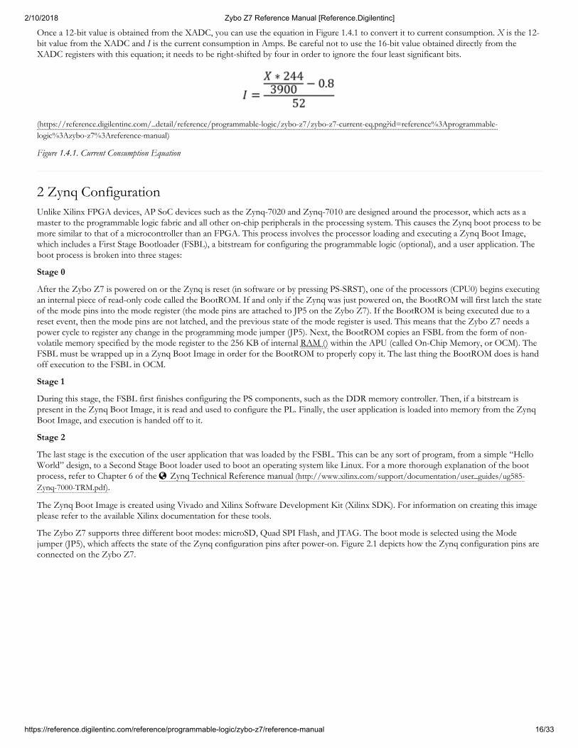
Once a 12-bit value is obtained from the XADC, you can use the equation in Figure 1.4.1 to convert it to current consumption. X is the 12-bit value from the XADC and I is the current consumption in Amps. Be careful not to use the 16-bit value obtained directly from theXADC registers with this equation; it needs to be right-shifted by four in order to ignore the four least significant bits.
(https://reference.digilentinc.com/_detail/reference/programmable-logic/zybo-z7/zybo-z7-current-eq.png?id=reference%3Aprogrammable-logic%3Azybo-z7%3Areference-manual)
Figure 1.4.1. Current Consumption Equation
Unlike Xilinx FPGA devices, AP SoC devices such as the Zynq-7020 and Zynq-7010 are designed around the processor, which acts as amaster to the programmable logic fabric and all other on-chip peripherals in the processing system. This causes the Zynq boot process to bemore similar to that of a microcontroller than an FPGA. This process involves the processor loading and executing a Zynq Boot Image,which includes a First Stage Bootloader (FSBL), a bitstream for configuring the programmable logic (optional), and a user application. Theboot process is broken into three stages:
Stage 0
After the Zybo Z7 is powered on or the Zynq is reset (in software or by pressing PS-SRST), one of the processors (CPU0) begins executingan internal piece of read-only code called the BootROM. If and only if the Zynq was just powered on, the BootROM will first latch the stateof the mode pins into the mode register (the mode pins are attached to JP5 on the Zybo Z7). If the BootROM is being executed due to areset event, then the mode pins are not latched, and the previous state of the mode register is used. This means that the Zybo Z7 needs apower cycle to register any change in the programming mode jumper (JP5). Next, the BootROM copies an FSBL from the form of non-volatile memory specified by the mode register to the 256 KB of internal RAM () within the APU (called On-Chip Memory, or OCM). TheFSBL must be wrapped up in a Zynq Boot Image in order for the BootROM to properly copy it. The last thing the BootROM does is handoff execution to the FSBL in OCM.
Stage 1
During this stage, the FSBL first finishes configuring the PS components, such as the DDR memory controller. Then, if a bitstream ispresent in the Zynq Boot Image, it is read and used to configure the PL. Finally, the user application is loaded into memory from the ZynqBoot Image, and execution is handed off to it.
Stage 2
The last stage is the execution of the user application that was loaded by the FSBL. This can be any sort of program, from a simple “HelloWorld” design, to a Second Stage Boot loader used to boot an operating system like Linux. For a more thorough explanation of the bootprocess, refer to Chapter 6 of the Zynq Technical Reference manual (http://www.xilinx.com/support/documentation/user_guides/ug585-Zynq-7000-TRM.pdf).
The Zynq Boot Image is created using Vivado and Xilinx Software Development Kit (Xilinx SDK). For information on creating this imageplease refer to the available Xilinx documentation for these tools.
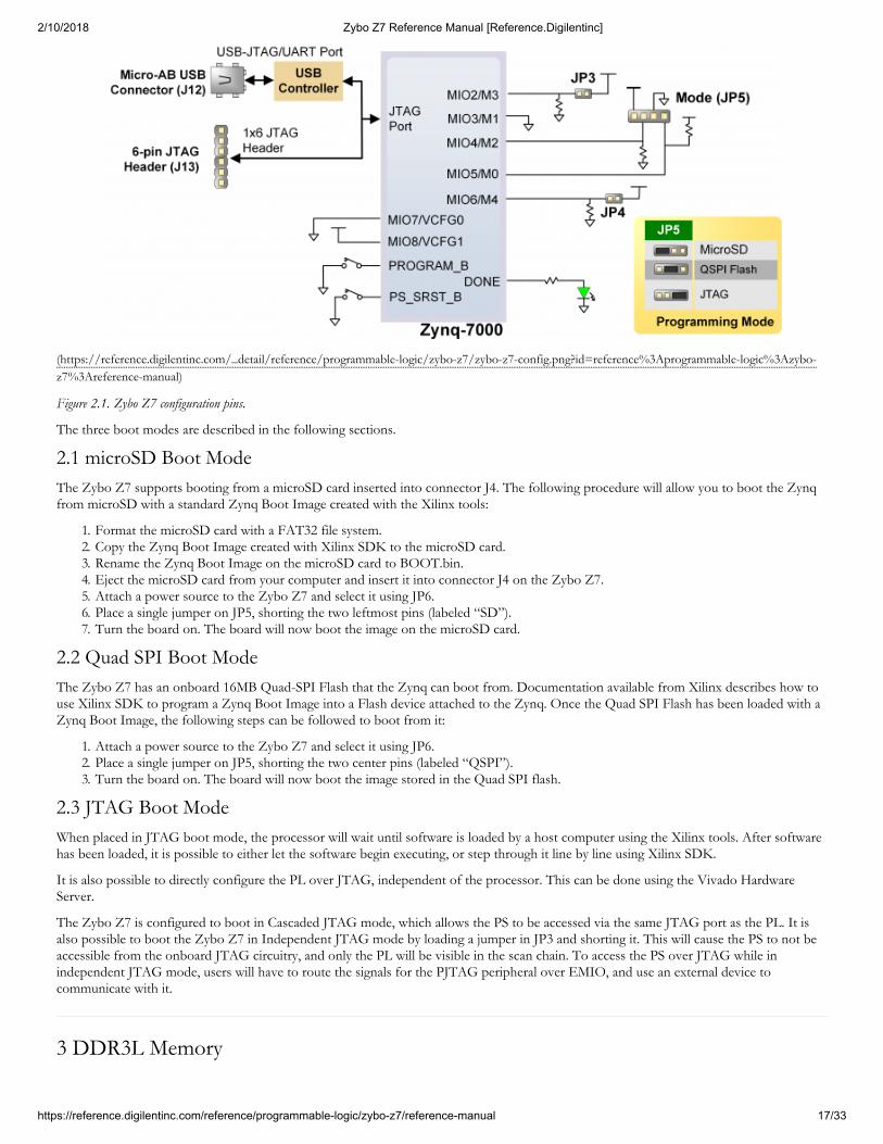
The Zybo Z7 supports three different boot modes: microSD, Quad SPI Flash, and JTAG. The boot mode is selected using the Modejumper (JP5), which affects the state of the Zynq configuration pins after power-on. Figure 2.1 depicts how the Zynq configuration pins areconnected on the Zybo Z7.
2 Zynq Configuration
2/10/2018 Zybo Z7 Reference Manual [Reference.Digilentinc]
https://reference.digilentinc.com/reference/programmable-logic/zybo-z7/reference-manual 17/33
(https://reference.digilentinc.com/_detail/reference/programmable-logic/zybo-z7/zybo-z7-config.png?id=reference%3Aprogrammable-logic%3Azybo-z7%3Areference-manual)
Figure 2.1. Zybo Z7 configuration pins.
The three boot modes are described in the following sections.
The Zybo Z7 supports booting from a microSD card inserted into connector J4. The following procedure will allow you to boot the Zynqfrom microSD with a standard Zynq Boot Image created with the Xilinx tools:
1. Format the microSD card with a FAT32 file system.2. Copy the Zynq Boot Image created with Xilinx SDK to the microSD card.3. Rename the Zynq Boot Image on the microSD card to BOOT.bin.4. Eject the microSD card from your computer and insert it into connector J4 on the Zybo Z7.5. Attach a power source to the Zybo Z7 and select it using JP6.6. Place a single jumper on JP5, shorting the two leftmost pins (labeled “SD”).7. Turn the board on. The board will now boot the image on the microSD card.
The Zybo Z7 has an onboard 16MB Quad-SPI Flash that the Zynq can boot from. Documentation available from Xilinx describes how touse Xilinx SDK to program a Zynq Boot Image into a Flash device attached to the Zynq. Once the Quad SPI Flash has been loaded with aZynq Boot Image, the following steps can be followed to boot from it:
1. Attach a power source to the Zybo Z7 and select it using JP6.2. Place a single jumper on JP5, shorting the two center pins (labeled “QSPI”).3. Turn the board on. The board will now boot the image stored in the Quad SPI flash.
When placed in JTAG boot mode, the processor will wait until software is loaded by a host computer using the Xilinx tools. After softwarehas been loaded, it is possible to either let the software begin executing, or step through it line by line using Xilinx SDK.
It is also possible to directly configure the PL over JTAG, independent of the processor. This can be done using the Vivado HardwareServer.
The Zybo Z7 is configured to boot in Cascaded JTAG mode, which allows the PS to be accessed via the same JTAG port as the PL. It isalso possible to boot the Zybo Z7 in Independent JTAG mode by loading a jumper in JP3 and shorting it. This will cause the PS to not beaccessible from the onboard JTAG circuitry, and only the PL will be visible in the scan chain. To access the PS over JTAG while inindependent JTAG mode, users will have to route the signals for the PJTAG peripheral over EMIO, and use an external device tocommunicate with it.
2.1 microSD Boot Mode
2.2 Quad SPI Boot Mode
2.3 JTAG Boot Mode
3 DDR3L Memory

2/10/2018 Zybo Z7 Reference Manual [Reference.Digilentinc]
https://reference.digilentinc.com/reference/programmable-logic/zybo-z7/reference-manual 18/33
The Zybo Z7 includes two Micron MT41K256M16HA-125 DDR3L memory components creating a single rank, 32-bit wide interface and atotal of 1 GiB (Gibi-byte, or 1,073,741,824 bytes) of capacity. The DDR3L is connected to the hard memory controller in the ProcessorSubsystem (PS), as outlined in the Zynq documentation.
The PS incorporates an AXI memory port interface, a DDR controller, the associated PHY, and a dedicated I/O bank. DDR3L memoryinterface speeds up to 533 MHz ()/1066 Mbps are supported.
Zybo Z7 was routed with 40 ohm (+/-10%) trace impedance for single-ended signals, and differential clock and strobes set to 80 ohms(+/-10%). A feature called DCI (Digitally Controlled Impedance) is used to match the drive strength and termination impedance of the PSpins to the trace impedance. On the memory side, each chip calibrates its on-die termination and drive strength using a 240 ohm resistor onthe ZQ pin.
Due to layout reasons, the two lower data byte groups (DQ[0-7], DQ[8-15]) were swapped. To the same effect, the data bits inside bytegroups were swapped as well. These changes are transparent to the user. During the whole design process the Xilinx PCB guidelines werefollowed.
Both the memory chips and the PS DDR bank are powered from the 1.35V supply. The mid-point reference of 0.675V is created with asimple resistor divider and is available to the Zynq as external reference.
For proper operation it is essential that the PS memory controller is configured properly. Settings range from the actual memory flavor tothe board trace delays. For your convenience, the Zybo Z7 Vivado board files are available on the Zybo Z7 Resource Center(https://reference.digilentinc.com/reference/programmable-logic/zybo-z7/start) and automatically configure the Zynq Processing System IP corewith the correct parameters.
For best DDR3L performance, DRAM training is enabled for write leveling, read gate, and read data eye options in the PS ConfigurationTool in Xilinx tools. Training is done dynamically by the controller to account for board delays, process variations and thermal drift.Optimum starting values for the training process are the board delays (propagation delays) for certain memory signals.
Board delays are specified for each of the byte groups. These parameters are board-specific and were calculated from the PCB trace lengthreports. The DQS to CLK Delay and Board Delay values are calculated specific to the Zybo Z7 memory interface PCB design.
For more details on memory controller operation, refer to the Xilinx Zynq Technical Reference manual(http://www.xilinx.com/support/documentation/user_guides/ug585-Zynq-7000-TRM.pdf).
The Zybo Z7 features a Spansion S25FL128S 4-bit Quad-SPI serial NOR flash. The key device attributes are:
Part number S25FL128S16 MiB (16,777,216 bytes)1-bit, 2-bit, and 4-bit bus widths supportedGeneral use clock speeds up to 100 MHz (), translating to 400 Mbps in Quad-SPI modeZynq configuration clock speeds up to 94 MHz ().Powered from 3.3V
The Flash memory is used to provide non-volatile code and data storage. It can be used to initialize the PS and PL of the Zynq device with aZynq Boot Image (also known as BOOT.BIN) generated using Xilinx tools such as Petalinux or Xilinx SDK. For information on bootingthe Zybo Z7 with a Zynq Boot image, see section “2.2 Quad SPI Boot Mode”.
The Flash is also commonly used to store non-configuration data needed by the application. If doing this from a bare-metal application, Theflash memory can be freely accessed using standalone libraries included with a Xilinx SDK BSP project. If doing this from a Petalinuxgenerated embedded Linux system, the Flash can be partitioned as desired and mounted/accessed like a standard MTD block device. Seethe Petalinux and Xilinx SDK documentation for more information.
The Flash connects to the Quad-SPI Flash controller of the Zynq-7000 PS via pins in MIO Bank 0/500 (specifically MIO[1:6,8]), asoutlined in the Zynq Technical Reference Manual. Quad-SPI feedback mode is used, thus qspi_sclk_fb_out/MIO[8] is left to freely toggleand is connected only to a 20K pull-up resistor to 3.3V. This allows a Quad-SPI clock frequency greater than FQSPICLK2. The details ofthese connections do not need to be known when using the Zybo Z7 Vivado Board files, as they will automatically configure your project towork correctly with the on-board Flash.
A globally unique MAC address is programmed into the One-Time-Programmable (OTP) region of the Flash on each Zybo Z7 at thefactory. For more information on this, see section “10 Ethernet”.
The OTP region also includes a factory-programmed read-only 128-bit random number. The very lowest address range [0x00;0x0F] can beread to access the random number. See the Spansion S25FL128S datasheet for information on this random number and accessing the OTPregion.
4 Quad-SPI Flash

2/10/2018 Zybo Z7 Reference Manual [Reference.Digilentinc]
https://reference.digilentinc.com/reference/programmable-logic/zybo-z7/reference-manual 19/33
The Zybo Z7 provides a 33.3333 MHz () clock to the Zynq PS_CLK input, which is used to generate the clocks for each of the PSsubsystems. The 33.3333 MHz () input allows the processor to operate at a maximum frequency of 667 MHz () and the DDR3 memorycontroller to operate at a maximum clock rate of 533 MHz () (1066 MT/s). The Zybo Z7 board files, available on the Zybo Z7 ResourceCenter (https://reference.digilentinc.com/reference/programmable-logic/zybo-z7/start), will automatically configure the Zynq processing systemIP core in Vivado to work with all PS attached devices, including the 33.3333 MHz () input oscillator.
The PS has a dedicated PLL capable of generating up to four reference clocks, each with settable frequencies, that can be used to clockcustom logic implemented in the PL. Additionally, The Zybo Z7 provides an external 125 MHz () reference clock directly to pin K17 of thePL. The external reference clock allows the PL to be used completely independently of the PS, which can be useful for simple applicationsthat do not require the processor.
The PL of the Zynq-Z7010 also includes two MMCM’s and two PLL’s that can be used to generate clocks with precise frequencies andphase relationships. Any of the four PS reference clocks or the 125 MHz () external reference clock can be used as an input to the MMCMsand PLLs. For a full description of the capabilities of the Zynq PL clocking resources, refer to the “7 Series FPGAs Clocking ResourcesUser Guide” available from Xilinx.
Xilinx offers the Clocking Wizard IP core to assist in integrating the MMCM's and PLL's into a design. This wizard will properly instantiatethe needed MMCMs and PLLs based on the desired frequencies and phase relationships specified by the user. The wizard will then outputan easy-to-use wrapper component around these clocking resources that can be inserted into the user’s design. The clocking wizard can beaccessed from within the Vivado and IP Integrator tools.
Figure 5.1 outlines the clocking scheme used on the Zybo Z7. Note that the reference clock output from the Ethernet PHY is used as the125 MHz () reference clock to the PL, in order to cut the cost of including a dedicated oscillator for this purpose. Keep in mind thatCLK125 will be disabled when the Ethernet PHY is held in hardware reset by driving the PHYRSTB signal low.
(https://reference.digilentinc.com/_detail/reference/programmable-logic/zybo-z7/zybo-z7-clock.png?id=reference%3Aprogrammable-logic%3Azybo-z7%3Areference-manual)
Figure 5.1. Zybo Z7 clocking.
The Zybo Z7 provides several different methods of resetting the Zynq-7000 device, as described in the following sections.
The Zynq PS supports external power-on reset signals. The power-on reset is the master reset of the entire chip. This signal resets everyregister in the device capable of being reset. The Zybo Z7 drives this signal from the PWRGD signal of the ADP5052 power regulator inorder to hold the system in reset until all power supplies are valid.
A red push button, labeled PROGB, toggles the Zynq-7000's PROG_B input. This resets the PL and causes DONE to be de-asserted. ThePL will remain unconfigured until it is reprogrammed by the processor or via JTAG.
5 Oscillators/Clocks
6 Reset Sources
6.1 Power-on Reset
6.2 Programmable Logic Reset
6.3 Processor Subsystem Reset

2/10/2018 Zybo Z7 Reference Manual [Reference.Digilentinc]
https://reference.digilentinc.com/reference/programmable-logic/zybo-z7/reference-manual 20/33
The external system reset button, labeled PS-SRST, resets the Zynq device without disturbing the debug environment. For example, theprevious break points set by the user remain valid after system reset. Due to security concerns, system reset erases all memory contentwithin the PS, including the On-Chip-Memory (OCM). The PL is also cleared during a system reset. System reset does not cause the bootmode strapping pins to be re-sampled. After changing boot moode jumpers a power cycle is needed to act on the new setting.
The Zybo Z7 includes an FTDI FT2232HQ USB-UART bridge (attached to connector J12) that lets you use PC applications tocommunicate with the board using standard COM port commands (or the tty interface in Linux). Drivers are automatically installed inWindows and newer versions of Linux when the Zybo Z7 is attached. Serial port data is exchanged with the Zynq using a two-wire serialport (TXD/RXD). After the drivers are installed, I/O commands can be used from the PC directed to the COM port to produce serial datatraffic on the Zynq pins. The port is tied to PS (MIO) pins and can be used in combination with the UART 1 controller.
The Zynq presets file (available in the Zybo Z7 Resource Center (https://reference.digilentinc.com/reference/programmable-logic/zybo-z7/start))takes care of mapping the correct MIO pins to the UART 1 controller and uses the following default protocol parameters: 115200 baud rate,1 stop bit, no parity, 8-bit character length.
Two on-board status LEDs provide visual feedback on traffic flowing through the port: the transmit LED () (LD11) and the receive LED ()(LD10). Signal names that imply direction are from the point-of-view of the DTE (Data Terminal Equipment), in this case the PC.
The FT2232HQ is also used as the controller for the Digilent USB-JTAG circuitry, but the USB-UART and USB-JTAG functions behaveentirely independent of one another. Programmers interested in using the UART functionality of the FT2232 within their design do notneed to worry about the JTAG circuitry interfering with the UART data transfers, and vice-versa. The combination of these two featuresinto a single device allows the Zybo Z7 to be programmed, communicated with via UART, and powered from a computer attached with asingle Micro USB cable.
The connections between the FT2232HQ and the Zynq-7000 are shown in Figure 7.1.
(https://reference.digilentinc.com/_detail/reference/programmable-logic/zybo-z7/zybo-z7-uart.png?id=reference%3Aprogrammable-logic%3Azybo-z7%3Areference-manual) Figure 7.1. UART Connections
The Zybo Z7 provides a microSD slot (J4) for non-volatile external memory storage as well as booting the Zynq. The slot is wired to Bank1/501 MIO[40-45], and also includes a card detect signal attached to MIO 47. On the PS side peripheral SDIO 0 is mapped out to thesepins and controls communication with the SD card. The pinout can be seen in Table 8.1. The peripheral controller supports 1-bit and 4-bitSD transfer modes, but does not support SPI mode. Based on the Zynq Technical Reference Manual(http://www.xilinx.com/support/documentation/user_guides/ug585-Zynq-7000-TRM.pdf), SDIO host mode is the only mode supported.
Signal Name Description Zynq Pin SD Slot Pin
SD_D0 Data[0] MIO42 7
SD_D1 Data[1] MIO43 8
SD_D2 Data[2] MIO44 1
SD_D3 Data[3] MIO45 2
7 USB-UART Bridge (Serial Port)
8 microSD Slot
2/10/2018 Zybo Z7 Reference Manual [Reference.Digilentinc]
https://reference.digilentinc.com/reference/programmable-logic/zybo-z7/reference-manual 21/33
SD_CCLK Clock MIO40 5
SD_CMD Command MIO41 3
SD_CD Card Detect MIO47 9
Table 8.1. MicroSD pinout
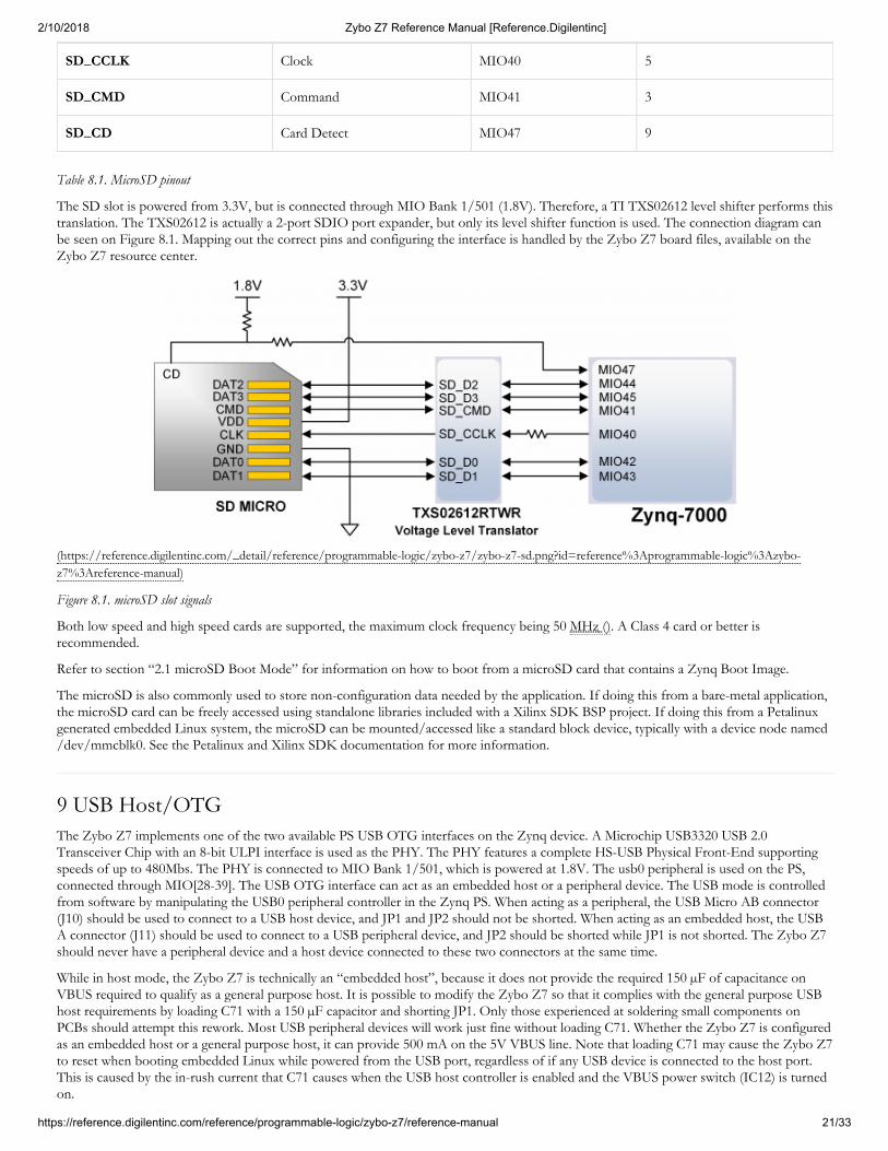
The SD slot is powered from 3.3V, but is connected through MIO Bank 1/501 (1.8V). Therefore, a TI TXS02612 level shifter performs thistranslation. The TXS02612 is actually a 2-port SDIO port expander, but only its level shifter function is used. The connection diagram canbe seen on Figure 8.1. Mapping out the correct pins and configuring the interface is handled by the Zybo Z7 board files, available on theZybo Z7 resource center.
(https://reference.digilentinc.com/_detail/reference/programmable-logic/zybo-z7/zybo-z7-sd.png?id=reference%3Aprogrammable-logic%3Azybo-z7%3Areference-manual)
Figure 8.1. microSD slot signals
Both low speed and high speed cards are supported, the maximum clock frequency being 50 MHz (). A Class 4 card or better isrecommended.
Refer to section “2.1 microSD Boot Mode” for information on how to boot from a microSD card that contains a Zynq Boot Image.
The microSD is also commonly used to store non-configuration data needed by the application. If doing this from a bare-metal application,the microSD card can be freely accessed using standalone libraries included with a Xilinx SDK BSP project. If doing this from a Petalinuxgenerated embedded Linux system, the microSD can be mounted/accessed like a standard block device, typically with a device node named/dev/mmcblk0. See the Petalinux and Xilinx SDK documentation for more information.
The Zybo Z7 implements one of the two available PS USB OTG interfaces on the Zynq device. A Microchip USB3320 USB 2.0Transceiver Chip with an 8-bit ULPI interface is used as the PHY. The PHY features a complete HS-USB Physical Front-End supportingspeeds of up to 480Mbs. The PHY is connected to MIO Bank 1/501, which is powered at 1.8V. The usb0 peripheral is used on the PS,connected through MIO[28-39]. The USB OTG interface can act as an embedded host or a peripheral device. The USB mode is controlledfrom software by manipulating the USB0 peripheral controller in the Zynq PS. When acting as a peripheral, the USB Micro AB connector(J10) should be used to connect to a USB host device, and JP1 and JP2 should not be shorted. When acting as an embedded host, the USBA connector (J11) should be used to connect to a USB peripheral device, and JP2 should be shorted while JP1 is not shorted. The Zybo Z7should never have a peripheral device and a host device connected to these two connectors at the same time.
While in host mode, the Zybo Z7 is technically an “embedded host”, because it does not provide the required 150 µF of capacitance onVBUS required to qualify as a general purpose host. It is possible to modify the Zybo Z7 so that it complies with the general purpose USBhost requirements by loading C71 with a 150 µF capacitor and shorting JP1. Only those experienced at soldering small components onPCBs should attempt this rework. Most USB peripheral devices will work just fine without loading C71. Whether the Zybo Z7 is configuredas an embedded host or a general purpose host, it can provide 500 mA on the 5V VBUS line. Note that loading C71 may cause the Zybo Z7to reset when booting embedded Linux while powered from the USB port, regardless of if any USB device is connected to the host port.This is caused by the in-rush current that C71 causes when the USB host controller is enabled and the VBUS power switch (IC12) is turnedon.
9 USB Host/OTG
2/10/2018 Zybo Z7 Reference Manual [Reference.Digilentinc]
https://reference.digilentinc.com/reference/programmable-logic/zybo-z7/reference-manual 22/33
Note that if your project uses the USB host feature (embedded or general purpose), then the Zybo Z7 is very likely to consume morecurrent than is allowed by a USB peripheral, causing it to periodically reset. When this occurs the PGOOD LED () will quickly flicker andthe DONE LED () will go low, indicating the PL is no longer programmed. To prevent this, power the Zybo Z7 by a 5V battery or walladapter capable of providing more power. See section “1 Power Supplies” for information on acceptable non-USB power sources.
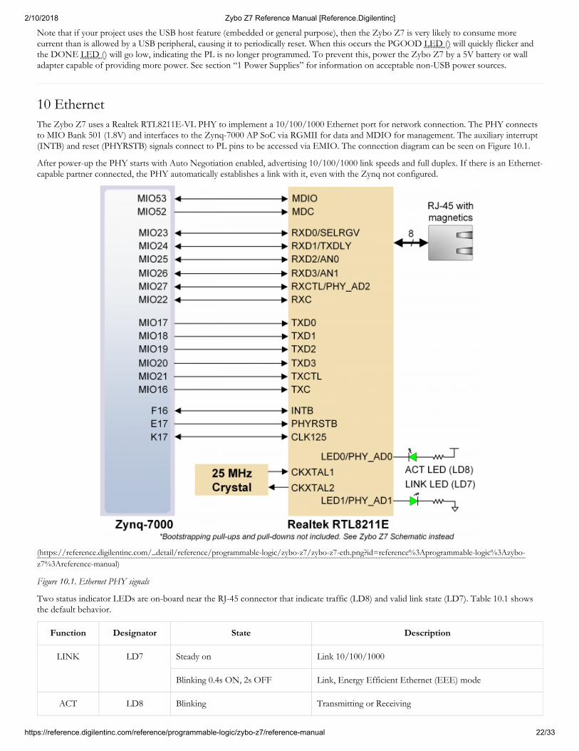
The Zybo Z7 uses a Realtek RTL8211E-VL PHY to implement a 10/100/1000 Ethernet port for network connection. The PHY connectsto MIO Bank 501 (1.8V) and interfaces to the Zynq-7000 AP SoC via RGMII for data and MDIO for management. The auxiliary interrupt(INTB) and reset (PHYRSTB) signals connect to PL pins to be accessed via EMIO. The connection diagram can be seen on Figure 10.1.
After power-up the PHY starts with Auto Negotiation enabled, advertising 10/100/1000 link speeds and full duplex. If there is an Ethernet-capable partner connected, the PHY automatically establishes a link with it, even with the Zynq not configured.
(https://reference.digilentinc.com/_detail/reference/programmable-logic/zybo-z7/zybo-z7-eth.png?id=reference%3Aprogrammable-logic%3Azybo-z7%3Areference-manual)
Figure 10.1. Ethernet PHY signals
Two status indicator LEDs are on-board near the RJ-45 connector that indicate traffic (LD8) and valid link state (LD7). Table 10.1 showsthe default behavior.
Function Designator State Description
LINK LD7 Steady on Link 10/100/1000
Blinking 0.4s ON, 2s OFF Link, Energy Efficient Ethernet (EEE) mode
ACT LD8 Blinking Transmitting or Receiving
10 Ethernet
2/10/2018 Zybo Z7 Reference Manual [Reference.Digilentinc]
https://reference.digilentinc.com/reference/programmable-logic/zybo-z7/reference-manual 23/33
Table 10.1. Ethernet status LEDs
The Zynq incorporates two independent Gigabit Ethernet Controllers. They implement a 10/100/1000 half/full duplex Ethernet MAC. Ofthese two, GEM 0 can be mapped to the MIO pins where the PHY interfaces. Since the MIO bank is powered from 1.8V, the RGMIIinterface uses 1.8V HSTL Class 1 drivers. For this I/O standard an external reference of 0.9V is provided in bank 501 (PS_MIO_VREF).Mapping out the correct pins and configuring the interface is handled by the Zybo Z7 Vivado board files.
Although the default power-up configuration of the PHY might be enough in most applications, the MDIO bus is available formanagement. The RTL8211E-VL is assigned the 5-bit address 00001 on the MDIO bus. With simple register read and write commands,status information can be read out or configuration changed. The Realtek PHY follows industry-standard register map for basicconfiguration.
The RGMII specification calls for the receive (RXC) and transmit clock (TXC) to be delayed relative to the data signals (RXD[0:3], RXCTLand TXD[0:3], TXCTL). Xilinx PCB guidelines also require this delay to be added. The RTL8211E-VL is capable of inserting a 2ns delay onboth the TXC and RXC so that board traces do not need to be made longer.
On an Ethernet network each node needs a unique MAC address. To this end, the one-time-programmable (OTP) region of the Quad-SPIflash has been programmed at the factory with a 48-bit globally unique EUI-48/64™ compatible identifier. The OTP address range[0x20;0x25] contains the identifier with the first byte in transmission byte order being at the lowest address. Refer to the Flash memorydatasheet (http://www.cypress.com/file/177966/download) for information on how to access the OTP regions. When using Petalinux, this isautomatically handled in the U-boot boot-loader, and the Linux system is automatically configured to use this unique MAC address. Theidentifier is also printed on a sticker found on the top-side of the Zybo Z7 right next to the mode jumper (JP5) and above the headphoneoutput jack.
For getting started using the ethernet port in a bare-metal application, Xilinx provides a lwip TCP/IP stack that can be automaticallygenerated in Xilinx SDK along with an echo server example. When using the Zybo Z7 with a Petalinux generated embedded Linux system,the ethernet port will automatically appear as a network device typically named eth0. See the Petalinux and Xilinx SDK documentation formore information.
For more low-level information on using the Zynq-7000 Gigabit Ethernet MAC, refer to the Xilinx Zynq Technical Reference Manual.
The Zybo Z7 contains one unbuffered source port (output, labeled HDMI TX), and one buffered sink port (input, labeled HDMI RX).Both ports use HDMI type-A receptacles with the data and clock signals terminated and connected to the Zynq PL. The buffer used on theHDMI RX port works by terminating, equalizing, conditioning, and forwarding the HDMI stream between the connector and FPGA pins.
The HDMI TX port does not include a buffer for improving signal integrity, but does include an HDMI multiplexer configured as a simpleswitch. This device is used to prevent displays from back-powering the Zybo Z7, and otherwise has no effect on functionality. The benefitthis adds is to make it possible to power cycle the Zybo Z7 while a display is attached to HDMI TX, which was not possible on the Zybo.
Both HDMI and DVI systems use the same TMDS signaling standard, directly supported by Zynq PL's user I/O infrastructure. Also,HDMI sources are backward compatible with DVI sinks, and vice versa. Thus, simple passive adaptors (available at most electronics stores)can be used to drive a DVI monitor or accept a DVI input. The HDMI receptacle only includes digital signals, so only DVI-D mode ispossible.
The 19-pin HDMI connectors include three differential data channels, one differential clock channel, five GND () connections, a one-wireConsumer Electronics Control (CEC) bus, a two-wire Display Data Channel (DDC) bus that is essentially an I2C bus, a Hot Plug Detect(HPD) signal, a 5V signal capable of delivering up to 50mA, and one reserved (RES) pin. All non-power signals are wired to the Zynq PLwith the exception of RES, and the CEC bus of the HDMI RX port on the Zybo Z7-10 (it is connected on the Zybo Z7-20).
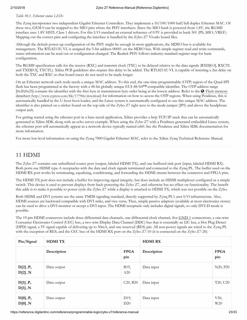
Pin/Signal HDMI TX HDMI RX
Description FPGApin
Description FPGApin
D[2]_P,D[2]_N
Data output B19,A20
Data input N20, P20
D[1]_P,D[1]_N
Data output C20, B20 Data input T20, U20
D[0]_P,D[0]_N
Data output D19,D20
Data input V20,W20
11 HDMI

2/10/2018 Zybo Z7 Reference Manual [Reference.Digilentinc]
https://reference.digilentinc.com/reference/programmable-logic/zybo-z7/reference-manual 24/33
CLK_P,CLK_N
Clock output H16,H17
Clock input U18,U19
CEC Consumer Electronics Control bidirectional(optional)
E19 CEC bidirectional (optional, N/A on ZyboZ7-10)
Y8
SCL, SDA DDC bidirectional (optional) G17,G18
DDC bidirectional W18,Y19
HPD/HPA Hot-plug detect input (inverted, optional) E18 Hot-plug assert output W19
Table 11.1. HDMI pin description and assignment
HDMI/DVI is a high-speed digital video stream interface using transition-minimized differential signaling (TMDS). To make proper use ofeither of the HDMI ports, a standard-compliant transmitter or receiver needs to be implemented in the Zynq PL. The implementationdetails are outside the scope of this manual. Check out the vivado-library IP Core repository on the Digilent github(https://github.com/Digilent) for ready-to-use reference IP. The IP cores for transmitting and receiving are called rgb2dvi and dvi2rgb,respectively.
Whenever a sink is ready and wishes to announce its presence, it connects the 5V0 supply pin to the HPD pin. On the Zybo Z7, this is doneby driving the Hot Plug Assert signal (HDMI_RX_HPD) high. Note this should only be done after a DDC channel slave has beenimplemented in the Zynq PL and is ready to transmit display data.
The Display Data Channel, or DDC, is a collection of protocols that enable communication between the display (sink) and graphics adapter(source). The DDC2B variant is based on I2C, the bus master being the source and the bus slave the sink. When a source detects high levelon the HPD pin, it queries the sink over the DDC bus for video capabilities. It determines whether the sink is DVI or HDMI-capable andwhat resolutions are supported. Only afterwards will video transmission begin. Refer to VESA E-DDC specifications for more information.IP supplied by Digilent in our Github repository vivado-library ( Digilent github (https://github.com/Digilent)) includes DDC support andsome pre-defined display descriptor data.
The Consumer Electronics Control, or CEC, is an optional protocol that allows control messages to be passed around on an HDMI chainbetween different products. A common use case is a TV passing control messages originating from a universal remote to a DVR or satellitereceiver. It is a one-wire protocol at 3.3V level connected to a Zynq PL user I/O pin. The wire can be controlled in an open-drain fashionallowing for multiple devices sharing a common CEC wire. Refer to the CEC addendum of HDMI 1.3 or later specifications for moreinformation.
An Analog Devices SSM2603 Audio Codec provides integrated digital audio processing to the Zynq-7000 AP SoC. It allows for stereorecord and playback at sample rates from 8 kHz () to 96 kHz ().
On the analog side, the codec connects to three 3.5 mm standard audio jacks. There are two inputs: a mono microphone and a stereo line in.There is one stereo output, the headphone jack. Analog power is provided by a dedicated linear power supply (IC5).
Audio Jack Description Channels Color
J5 Headphone Out Stereo Black
J6 Microphone In Mono Pink
J7 Line In Stereo Light Blue
Table 12.1. Analog audio signals
The digital interface of the SSM2603 is wired to the programmable logic side of the Zynq. Audio data is transferred via the I²S protocol.Configuration is done over an I2C bus. The device address of the SSM2603 is 0011010b. All digital I/O are 3.3V level and connect to a3.3V-powered FPGA bank.
11.1 TMDS Signals
11.2 Auxiliary signals
12 Audio
2/10/2018 Zybo Z7 Reference Manual [Reference.Digilentinc]
https://reference.digilentinc.com/reference/programmable-logic/zybo-z7/reference-manual 25/33
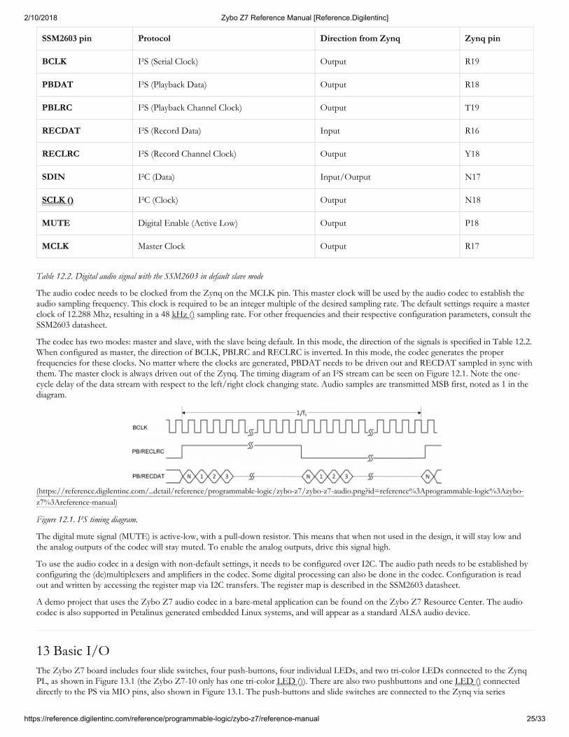
SSM2603 pin Protocol Direction from Zynq Zynq pin
BCLK I²S (Serial Clock) Output R19
PBDAT I²S (Playback Data) Output R18
PBLRC I²S (Playback Channel Clock) Output T19
RECDAT I²S (Record Data) Input R16
RECLRC I²S (Record Channel Clock) Output Y18
SDIN I²C (Data) Input/Output N17
SCLK () I²C (Clock) Output N18
MUTE Digital Enable (Active Low) Output P18
MCLK Master Clock Output R17
Table 12.2. Digital audio signal with the SSM2603 in default slave mode
The audio codec needs to be clocked from the Zynq on the MCLK pin. This master clock will be used by the audio codec to establish theaudio sampling frequency. This clock is required to be an integer multiple of the desired sampling rate. The default settings require a masterclock of 12.288 Mhz, resulting in a 48 kHz () sampling rate. For other frequencies and their respective configuration parameters, consult theSSM2603 datasheet.
The codec has two modes: master and slave, with the slave being default. In this mode, the direction of the signals is specified in Table 12.2.When configured as master, the direction of BCLK, PBLRC and RECLRC is inverted. In this mode, the codec generates the properfrequencies for these clocks. No matter where the clocks are generated, PBDAT needs to be driven out and RECDAT sampled in sync withthem. The master clock is always driven out of the Zynq. The timing diagram of an I²S stream can be seen on Figure 12.1. Note the one-cycle delay of the data stream with respect to the left/right clock changing state. Audio samples are transmitted MSB first, noted as 1 in thediagram.
(https://reference.digilentinc.com/_detail/reference/programmable-logic/zybo-z7/zybo-z7-audio.png?id=reference%3Aprogrammable-logic%3Azybo-z7%3Areference-manual)
Figure 12.1. I²S timing diagram.
The digital mute signal (MUTE) is active-low, with a pull-down resistor. This means that when not used in the design, it will stay low andthe analog outputs of the codec will stay muted. To enable the analog outputs, drive this signal high.
To use the audio codec in a design with non-default settings, it needs to be configured over I2C. The audio path needs to be established byconfiguring the (de)multiplexers and amplifiers in the codec. Some digital processing can also be done in the codec. Configuration is readout and written by accessing the register map via I2C transfers. The register map is described in the SSM2603 datasheet.
A demo project that uses the Zybo Z7 audio codec in a bare-metal application can be found on the Zybo Z7 Resource Center. The audiocodec is also supported in Petalinux generated embedded Linux systems, and will appear as a standard ALSA audio device.
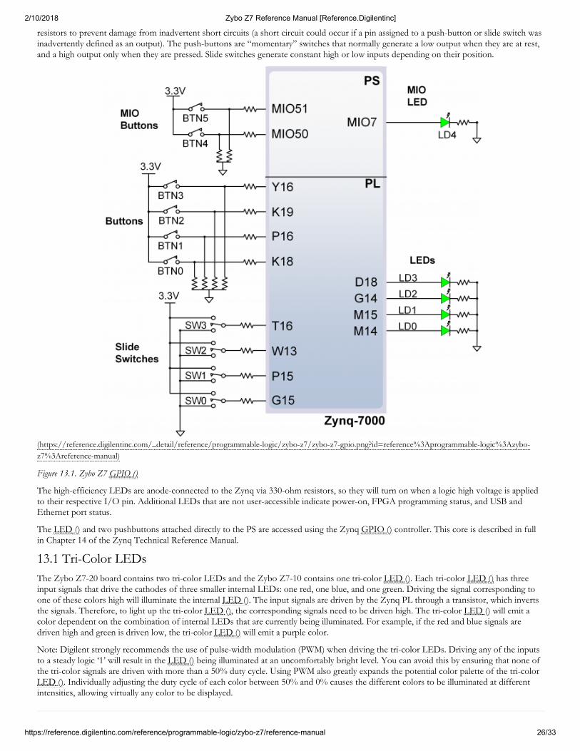
The Zybo Z7 board includes four slide switches, four push-buttons, four individual LEDs, and two tri-color LEDs connected to the ZynqPL, as shown in Figure 13.1 (the Zybo Z7-10 only has one tri-color LED ()). There are also two pushbuttons and one LED () connecteddirectly to the PS via MIO pins, also shown in Figure 13.1. The push-buttons and slide switches are connected to the Zynq via series
13 Basic I/O
2/10/2018 Zybo Z7 Reference Manual [Reference.Digilentinc]
https://reference.digilentinc.com/reference/programmable-logic/zybo-z7/reference-manual 26/33
resistors to prevent damage from inadvertent short circuits (a short circuit could occur if a pin assigned to a push-button or slide switch wasinadvertently defined as an output). The push-buttons are “momentary” switches that normally generate a low output when they are at rest,and a high output only when they are pressed. Slide switches generate constant high or low inputs depending on their position.
(https://reference.digilentinc.com/_detail/reference/programmable-logic/zybo-z7/zybo-z7-gpio.png?id=reference%3Aprogrammable-logic%3Azybo-z7%3Areference-manual)
Figure 13.1. Zybo Z7 GPIO ()
The high-efficiency LEDs are anode-connected to the Zynq via 330-ohm resistors, so they will turn on when a logic high voltage is appliedto their respective I/O pin. Additional LEDs that are not user-accessible indicate power-on, FPGA programming status, and USB andEthernet port status.
The LED () and two pushbuttons attached directly to the PS are accessed using the Zynq GPIO () controller. This core is described in fullin Chapter 14 of the Zynq Technical Reference Manual.
The Zybo Z7-20 board contains two tri-color LEDs and the Zybo Z7-10 contains one tri-color LED (). Each tri-color LED () has threeinput signals that drive the cathodes of three smaller internal LEDs: one red, one blue, and one green. Driving the signal corresponding toone of these colors high will illuminate the internal LED (). The input signals are driven by the Zynq PL through a transistor, which invertsthe signals. Therefore, to light up the tri-color LED (), the corresponding signals need to be driven high. The tri-color LED () will emit acolor dependent on the combination of internal LEDs that are currently being illuminated. For example, if the red and blue signals aredriven high and green is driven low, the tri-color LED () will emit a purple color.
Note: Digilent strongly recommends the use of pulse-width modulation (PWM) when driving the tri-color LEDs. Driving any of the inputsto a steady logic ‘1’ will result in the LED () being illuminated at an uncomfortably bright level. You can avoid this by ensuring that none ofthe tri-color signals are driven with more than a 50% duty cycle. Using PWM also greatly expands the potential color palette of the tri-colorLED (). Individually adjusting the duty cycle of each color between 50% and 0% causes the different colors to be illuminated at differentintensities, allowing virtually any color to be displayed.
13.1 Tri-Color LEDs
2/10/2018 Zybo Z7 Reference Manual [Reference.Digilentinc]
https://reference.digilentinc.com/reference/programmable-logic/zybo-z7/reference-manual 27/33
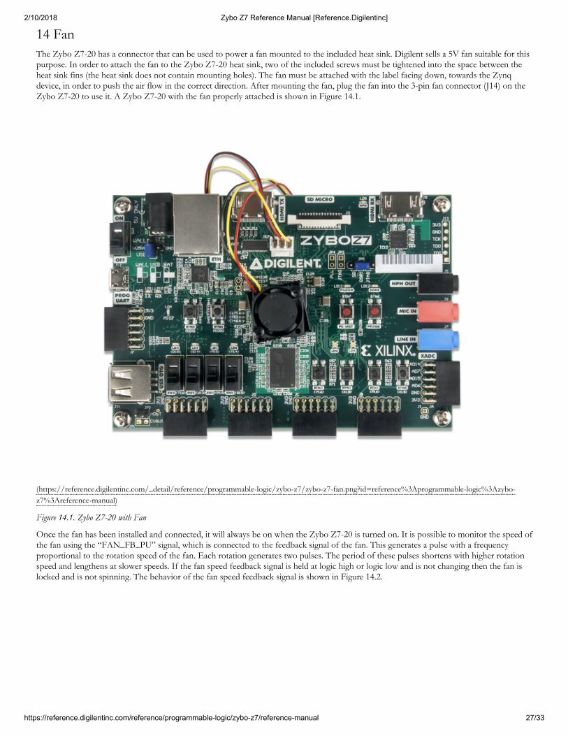
The Zybo Z7-20 has a connector that can be used to power a fan mounted to the included heat sink. Digilent sells a 5V fan suitable for thispurpose. In order to attach the fan to the Zybo Z7-20 heat sink, two of the included screws must be tightened into the space between theheat sink fins (the heat sink does not contain mounting holes). The fan must be attached with the label facing down, towards the Zynqdevice, in order to push the air flow in the correct direction. After mounting the fan, plug the fan into the 3-pin fan connector (J14) on theZybo Z7-20 to use it. A Zybo Z7-20 with the fan properly attached is shown in Figure 14.1.
(https://reference.digilentinc.com/_detail/reference/programmable-logic/zybo-z7/zybo-z7-fan.png?id=reference%3Aprogrammable-logic%3Azybo-z7%3Areference-manual)
Figure 14.1. Zybo Z7-20 with Fan
Once the fan has been installed and connected, it will always be on when the Zybo Z7-20 is turned on. It is possible to monitor the speed ofthe fan using the “FAN_FB_PU” signal, which is connected to the feedback signal of the fan. This generates a pulse with a frequencyproportional to the rotation speed of the fan. Each rotation generates two pulses. The period of these pulses shortens with higher rotationspeed and lengthens at slower speeds. If the fan speed feedback signal is held at logic high or logic low and is not changing then the fan islocked and is not spinning. The behavior of the fan speed feedback signal is shown in Figure 14.2.
14 Fan

2/10/2018 Zybo Z7 Reference Manual [Reference.Digilentinc]
https://reference.digilentinc.com/reference/programmable-logic/zybo-z7/reference-manual 28/33
(https://reference.digilentinc.com/_detail/reference/programmable-logic/zybo-z7/fan_fig.png?id=reference%3Aprogrammable-logic%3Azybo-z7%3Areference-manual)
Figure 14.2. Fan Speed Feedback Signal
It is possible to monitor the temperature of the Zynq device during operation over JTAG from the hardware server in Vivado. Themaximum recommended operating temperature for the Zynq-7020 device is 85°C. If your design causes the temperature of the Zynq toapproach the maximum, Digilent recommends you turn off the Zybo Z7-20 and attach a fan before running your design again. Thetemperature that the Zynq reaches is largely based on the number of resources used in the Zynq PL and the rate at which they are switching.Most designs should not reach temperatures that will require a fan. When powering the Zybo Z7-20 from USB, a fan is not necessarybecause the current limit will cause the board to reset before a dangerous amount of heat can be generated.
The fan connector is not loaded on the Zybo Z7-10 because additional cooling is typically not needed with the fewer available FPGAresources.
The Pcam port included on the Zybo Z7 is a 15-pin, 1 mm pitch, zero insertion force (ZIF) connector designed specifically for attachingcamera sensor modules to host systems. The Pcam connector pin-out is rigidly defined and includes a two lane MIPI CSI-2 bus for cameradata, an I2C bus for camera configuration, two additional general purpose signals, and 3.3 V for powering the camera module, as depicted inFigure 15.1 and Table 15.1. Digilent is developing a catalog of Pcam peripheral camera modules with various different types of sensors thatall conform to this pin-out. The pin-out was also chosen so that many camera modules designed to work with the Raspberry Pi will alsowork when connected to the Pcam port.
(https://reference.digilentinc.com/_detail/reference/programmable-logic/zybo-z7/zybo-z7-pcam-pins.png?id=reference%3Aprogrammable-logic%3Azybo-z7%3Areference-manual) Figure 15.1. Pcam Pin-out
Pin Number Function Zybo Z7 Connection Details
1 GND () GND ()
2 MIPI CSI-2 Lane 0 (-) Terminated and connected to 2 FPGA pins as described in XAPP894
3 MIPI CSI-2 Lane 0 (+) Terminated and connected to 2 FPGA pins as described in XAPP894
4 GND () GND ()
5 MIPI CSI-2 Lane 1 (-) Terminated and connected to 2 FPGA pins as described in XAPP894
15 Pcam Port

2/10/2018 Zybo Z7 Reference Manual [Reference.Digilentinc]
https://reference.digilentinc.com/reference/programmable-logic/zybo-z7/reference-manual 29/33
Pin Number Function Zybo Z7 Connection Details
6 MIPI CSI-2 Lane 1 (+) Terminated and connected to 2 FPGA pins as described in XAPP894
7 GND () GND ()
8 MIPI CSI-2 Clock (-) Terminated and connected to 2 FPGA pins as described in XAPP894
9 MIPI CSI-2 Clock (+) Terminated and connected to 2 FPGA pins as described in XAPP894
10 GND () GND ()
11 GPIO ()/Power enable Direct Connection to FPGA, usage module-dependent
12 GPIO ()/Clock feedback Direct Connection to FPGA, usage module-dependent
13 SCL Direct Connection to FPGA, with 1.5 KOhm Pull-up
14 SDA Direct Connection to FPGA, with 1.5 KOhm Pull-up
15 3V3 3.3 V Power rail
Table 15.1. Pcam Pin-out
Pcam modules are connected to the Pcam host port using a flexible flat cable (FFC). To connect the cable to the Zybo Z7 follow theseinstruction (Figure 15.2 depicts each step):
1. Locate the Pcam connector between the two HDMI ports.2. Pull directly up on the off-white colored tab to open the connector.3. Insert the FFC with the contacts facing the top edge, away from the center of the Zybo Z7.4. Ensure the FFC is fully inserted.5. Gently press down on both sides of the off-white colored tab to latch the FFC into the connector.6. The FFC is now connected properly.
(https://reference.digilentinc.com/_detail/reference/programmable-logic/zybo-z7/zybo-z7-pcam-attach.png?id=reference%3Aprogrammable-logic%3Azybo-z7%3Areference-manual)
Figure 15.2. Attaching a Pcam
2/10/2018 Zybo Z7 Reference Manual [Reference.Digilentinc]
https://reference.digilentinc.com/reference/programmable-logic/zybo-z7/reference-manual 30/33
The MIPI CSI-2 bus is passively terminated on the Zybo Z7 and connected directly to the Zynq PL. The guidelines described in Xilinxapplication note XAPP894 D-PHY solutions (https://www.xilinx.com/support/documentation/application_notes/xapp894-d-phy-solutions.pdf)were followed in order to implement a compatible D-PHY receiver using the Zynq. The interface is tested to operate at up to 672 Mbps oneach lane. Speeds up to 950 Mbps on each lane are possible based on the Zynq-7000 timing specifications, however they are not validatedon the Zybo Z7.
A MIPI CSI-2 Receiver IP core (https://www.xilinx.com/products/intellectual-property/ef-di-mipi-csi-rx.html) is available from Xilinx, andincludes embedded Linux support. It requires a license in order to use, however it is possible to obtain an evaluation license from Xilinx forfree.
A reference implementation with a basic feature set of both D-PHY and CSI-2 will be provided by Digilent in our Github repository.
Note: Digilent does not currently have any Pcam modules available for sale, and therefore no demo content either. The expected release date of our first Pcammodule is at the end of 2017. This Pcam module will be released with demo content for use with the Zybo Z7. We apologize for the delay.
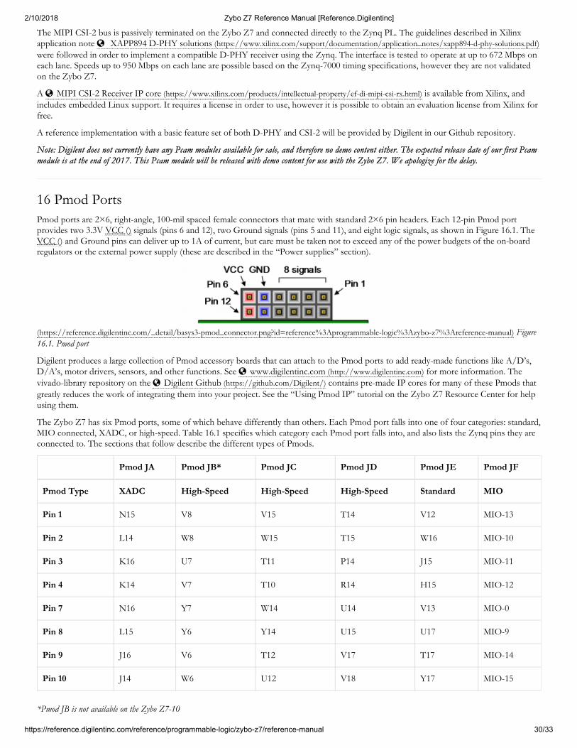
Pmod ports are 2×6, right-angle, 100-mil spaced female connectors that mate with standard 2×6 pin headers. Each 12-pin Pmod portprovides two 3.3V VCC () signals (pins 6 and 12), two Ground signals (pins 5 and 11), and eight logic signals, as shown in Figure 16.1. TheVCC () and Ground pins can deliver up to 1A of current, but care must be taken not to exceed any of the power budgets of the on-boardregulators or the external power supply (these are described in the “Power supplies” section).
(https://reference.digilentinc.com/_detail/basys3-pmod_connector.png?id=reference%3Aprogrammable-logic%3Azybo-z7%3Areference-manual) Figure16.1. Pmod port
Digilent produces a large collection of Pmod accessory boards that can attach to the Pmod ports to add ready-made functions like A/D’s,D/A’s, motor drivers, sensors, and other functions. See www.digilentinc.com (http://www.digilentinc.com) for more information. Thevivado-library repository on the Digilent Github (https://github.com/Digilent/) contains pre-made IP cores for many of these Pmods thatgreatly reduces the work of integrating them into your project. See the “Using Pmod IP” tutorial on the Zybo Z7 Resource Center for helpusing them.
The Zybo Z7 has six Pmod ports, some of which behave differently than others. Each Pmod port falls into one of four categories: standard,MIO connected, XADC, or high-speed. Table 16.1 specifies which category each Pmod port falls into, and also lists the Zynq pins they areconnected to. The sections that follow describe the different types of Pmods.
Pmod JA Pmod JB* Pmod JC Pmod JD Pmod JE Pmod JF
Pmod Type XADC High-Speed High-Speed High-Speed Standard MIO
Pin 1 N15 V8 V15 T14 V12 MIO-13
Pin 2 L14 W8 W15 T15 W16 MIO-10
Pin 3 K16 U7 T11 P14 J15 MIO-11
Pin 4 K14 V7 T10 R14 H15 MIO-12
Pin 7 N16 Y7 W14 U14 V13 MIO-0
Pin 8 L15 Y6 Y14 U15 U17 MIO-9
Pin 9 J16 V6 T12 V17 T17 MIO-14
Pin 10 J14 W6 U12 V18 Y17 MIO-15
*Pmod JB is not available on the Zybo Z7-10
16 Pmod Ports

2/10/2018 Zybo Z7 Reference Manual [Reference.Digilentinc]
https://reference.digilentinc.com/reference/programmable-logic/zybo-z7/reference-manual 31/33
Table 16.1. Zybo Z7 Pmod Pinout
The standard Pmod ports are connected to the Zynq PL via 200 Ohm series resistors. The series resistors prevent short circuits that canoccur if the user accidentally drives a signal that is supposed to be used as an input. The downside to this added protection is that theseresistors can limit the maximum switching speed of the data signals. If the Pmod being used does not require high-speed access, then thestandard Pmod port should be used to help prevent damage to the devices.
The MIO Pmod port is connected to the MIO bus in the Zynq PS via 200 Ohm series resistors. Like the standard Pmod port, these seriesresistors add protection at the cost of maximum switching speed. Since these data signals are connected to the MIO interface, they can onlybe accessed by the PS peripheral controller cores. The GPIO (), UART, I2C, and SPI cores can all be used to drive devices connected to thisPmod. Note that the pin layout of the UART and I2C cores will not align perfectly with the typical Pmod pinouts for these interfaces. Thismeans that UART or I2C devices connected to this Pmod may require some of the pins to be swapped around externally using individualwires between the Zybo Z7 and the Pmod.
The Pmod port labeled “XADC” is wired to the auxiliary analog input pins of the PL. Depending on the Zynq PL configuration, this portcan be used to input differential analog signals to the analog-to-digital converter inside the Zynq XADC core. Any or all pairs in the port canbe configured either as analog input or digital input-output.
In analog input mode, the voltage on these pins must be limited to 1V peak-to-peak. In digital mode, the regular VCCO-dependent limitsapply. See Xilinx datasheets for more information.
The Dual Analog/Digital Pmod on the Zybo Z7 differs from the rest in the routing of its traces. The eight data signals are grouped intofour pairs, with the pairs routed closely coupled for better analog noise immunity. Pins 1 and 7, pins 2 and 8, pins 3 and 9, and pins 4 and 10are paired up. Furthermore, each pair has a partially loaded anti-alias filter laid out on the PCB. The filter does not have capacitors C101-C104 loaded. In designs where such filters are desired, the capacitors can be manually loaded by the user.
NOTE: The coupled routing and the anti-alias filters might limit the data speeds when used for digital signals.
The XADC core within the Zynq is a dual channel 12-bit analog-to-digital converter capable of operating at 1 MSPS. Either channel can bedriven by any of the auxiliary analog input pairs connected to the XADC port. The XADC core is controlled and accessed from the PL viathe Dynamic Reconfiguration Port (DRP). The DRP also provides access to voltage monitors that are present on each of the Zynq's powerrails, and a temperature sensor that is internal to the Zynq. For more information on using the XADC core, refer to the Xilinx documenttitled “7 Series FPGAs and Zynq-7000 All Programmable SoC XADC Dual 12-Bit 1 MSPS Analog-to-Digital Converter.” It is also possibleto access the XADC core directly using the PS, via the “PS-XADC” interface. This interface is described in full in chapter 30 of the ZynqTechnical Reference Manual.
The High-speed Pmod ports use the standard Pmod connector, but have their data signals routed as impedance matched differential pairsfor maximum switching speeds. They have pads for loading resistors for added protection, but the Zybo Z7 ships with these loaded as 0-Ohm shunts. With the series resistors shunted, these Pmods offer no protection against short circuits, but allow for much faster switchingspeeds. The signals are paired to the adjacent signals in the same row: pins 1 and 2, pins 3 and 4, pins 7 and 8, and pins 9 and 10.
Traces are routed 80 ohm (+/- 10%) differential.
These ports should be used only when high speed signaling is required or the other suitable ports are occupied. If used as single-ended,coupled pairs may have significant cross-talk. In applications where this is a concern, the standard Pmod port should be used. Anotheroption would be to ground one of the signals and use its pair for the signal-ended signal.
Since the High-Speed Pmods have 0-ohm shunts instead of protection resistors, the operator must take precaution to ensure that they donot cause any shorts.
rm (https://reference.digilentinc.com/tag/rm?do=showtag&tag=rm), doc (https://reference.digilentinc.com/tag/doc?do=showtag&tag=doc), zybo-z7(https://reference.digilentinc.com/tag/zybo-z7?do=showtag&tag=zybo-z7)
16.1 Standard Pmod
16.2 MIO Pmod
16.3 Dual Analog/Digital Pmod (XADC Pmod)
16.4 High-Speed Pmod
First Name
Last Name
Email Address
Subscribe to our Newsletter
2/10/2018 Zybo Z7 Reference Manual [Reference.Digilentinc]
https://reference.digilentinc.com/reference/programmable-logic/zybo-z7/reference-manual 32/33
Email ddress
Submit
Xilinx UniversityProgram(https://store.digilentinc.com/partners/xilinx-university-program/)Technology Partners(https://store.digilentinc.com/technology-partners/)Distributors(https://store.digilentinc.com/our-distributors/)
Our Partners
Technical SupportForum(https://forum.digilentinc.com)Reference Wiki(https://reference.digilentinc.com)Contact Us(https://store.digilentinc.com/contact-us/)
Help
Videos(https://youtube.com/user/digilentinc)FAQ(https://resource.digilentinc.com/verify/faq)Store Info(https://store.digilentinc.com/store-info/)
Customer Info
About Us(https://store.digilentinc.com/ppageid=26)Shipping & Returns(https://store.digilentinc.com/returns/)Legal(https://store.digilentinc.com/lJobs(https://store.digilentinc.com/jInternships(https://store.digilentinc.com/i
Company Info
(https://twitter.com/digilentinc)
(https://www.facebook.com/Digilent)
(https://www.youtube.com/user/DigilentInc)
(https://instagram.com/digilentinc)
(https://github.com/digilent)
Connect With Us
2/10/2018 Zybo Z7 Reference Manual [Reference.Digilentinc]
https://reference.digilentinc.com/reference/programmable-logic/zybo-z7/reference-manual 33/33
(https://www.reddit.com/r/digilent)
(https://www.linkedin.com/company/1454013)
(https://www.flickr.com/photos/127815101@N07)