© copyright 2009 xilinx copyright 2012 xilinx august 2012 zynq-7000 all programmable soc product...
TRANSCRIPT
© Copyright 2009 XilinxCopyright 2012 Xilinx
August 2012
Zynq-7000 All Programmable SoC Product Overview
The SW, HW and IO Programmable Platform

Copyright 2012 Xilinx
Breakthrough Processing Platform– Higher system performance, lower total power– Flexible and scalable solution
Industry Standard Design Environments– Well defined SW programming model– Familiar SW & HW design flows
Flexible Accelerators and IP– World class 28nm unified Programmable Logic– Standard AMBA® 4 AXI interfaces
Broad Ecosystem Support– Tools, OS’s & IPs– Middleware, codecs– System integrators and training partners.
Page 2
Introducing the Zynq™-7000 All Programmable SoC
Familiar Processing System + Scalable Programmable Logic

Copyright 2012 Xilinx
Next level of Programmable System Integration– All programmable (Hardware and Software) processing platform – ARM Cortex™-A9 MPCore™ Processing System with hardened peripherals,
ADC and 28nm scalable optimized programmable logic
Increased System Performance– 1 GHz, dual core processors with NEON and vector floating point units– 7 series programmable logic (PL) with built-in DSP– High bandwidth, low latency connects enable acceleration of key functions
BOM Cost Advantage in an cost optimized 28nm platform– Integration for component reduction, PCB simplification and area reduction– Platform approach enables aggregation of volumes over several projects
Low Total Power solution– Industry-leading ARM processors maximize MHz/W and low power states– 28nm HPL process and Integration provides ultra-lower power data transfers– Software and Hardware programmable power control and operating modes
Accelerated Design Productivity for TTM and TIM advantage– Industry standard HW and SW development tools for fast Time-To-Market– Flexible and scalable platform enables extended Time-In-Market– Extensive ecosystem of tools and solutions partners
Page 3
Value of the Zynq-7000 All Programmable SoC

Copyright 2012 Xilinx
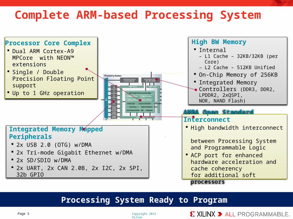
Complete ARM®-based Processing System– Dual ARM Cortex™-A9 MPCore™, processor centric– Integrated memory controllers & peripherals– Fully autonomous to the Programmable Logic
Tightly Integrated Programmable Logic– Used to extend Processing System– High performance ARM AXI interfaces– Scalable density and performance
Flexible Array of I/O– Wide range of external multi-standard I/O– High performance integrated serial transceivers– Analog-to-Digital Converter inputs
Page 4
Zynq-7000 Family Highlights
Software & Hardware & IO Programmable
7 SeriesProgrammable
Logic
Common Peripherals
CustomPeripherals
Common Accelerators
Custom Accelerators
CommonPeripherals
ProcessingSystem
MemoryInterfaces
ARM®
Dual Cortex-A9 MPCore™ System
Copyright 2012 Xilinx
AMBA Open Standard Interconnect High bandwidth interconnect
between Processing System and Programmable Logic
ACP port for enhanced hardware acceleration and cache coherency for additional soft processors
Page 5
Complete ARM-based Processing System
Processing System Ready to Program
Integrated Memory Mapped Peripherals 2x USB 2.0 (OTG) w/DMA 2x Tri-mode Gigabit Ethernet w/DMA 2x SD/SDIO w/DMA 2x UART, 2x CAN 2.0B, 2x I2C, 2x SPI, 32b GPIO
Processor Core Complex Dual ARM Cortex-A9 MPCore
with NEON™ extensions Single / Double Precision
Floating Point support Up to 1 GHz operation
High BW Memory Internal
– L1 Cache – 32KB/32KB (per Core)– L2 Cache – 512KB Unified
On-Chip Memory of 256KB Integrated Memory Controllers
(DDR3, DDR2, LPDDR2, 2xQSPI, NOR, NAND Flash)

Copyright 2012 Xilinx
On-Chip Memory (OCM)– Dual-ported 256KB– Low-latency CPU access– Accessible by DMAs, Programmable
Logic, etc.
Powerful Application Processor at HeartThe Application Processor Unit (APU)
Page 6
MIO
NEON™/ FPU Engine
Cortex™-A9 MPCore™32/32 KB I/D Caches
NEON™/ FPU Engine
Cortex™-A9 MPCore™32/32 KB I/D Caches
512KB L2 CacheSnoop Control
Unit256 KB OCM
Interrupt Controller, Timers, DMA, Debug, etc.
Dual ARM Cortex-A9 MPCore with NEON extensions– Up to 1 GHz operation (7030 & 7045)– 2.5 DMIPS/MHz per core– Multi-issue (up to 4), Out-of-order,
Speculative– Separate 32KB Instruction and Data Caches
with Parity
Snoop Control Unit– L1 Cache Snoop Control
• Snoop filtering monitors cache traffic• Accelerator Coherency Port
Level 2 Cache and Controller– Shared 512 KB Cache with parity– Lockable

Copyright 2012 Xilinx
DDR controller– DDR3, DDR2, and LPDDR2– 16 bit or 32 bit wide; ECC on 16 bit – DDR3 @ up to DDR1333– DDR2 @ up to DDR800– LPDDR2 @ up to DDR800– 73 dedicated DDR pins
NAND Controller– ECC – 8 bit or 16 bit data widths
NOR/SRAM Controller– 8 bit data width
Quad SPI (QSPI) Controller– Up to 2 QSPI parallel memories for high-
speed boot and configuration
Processing System External MemoriesBuilt-in Controllers and dedicated DDR Pins
32 bit 16 bit
4 x 8 bit 2 x 8 bit
2 x 16 bit 1 x 16 bit
1x 32bit NA
NANDCTRL
NOR /SRAM CTRL
QSPICTRL
To MIO
2 Chip Selects
APU
DDR Controller
LegendArrow direction shows control, Data flows both directionsAXI3 64 bit / APB 32 bit
From L2 Cache
Controller
From Central Interconnect
2 Dedicated to Programmable
Logic
Page 7

Copyright 2012 Xilinx
Two USB 2.0 OTG/Device/Host
Two Tri- Mode GigE (10/100/1000)
Two SD/SDIO interfaces
Two CAN 2.0B, SPI , I2C , UART
Four GPIO 32bit Blocks
Multiplexed Input/Output (MIO)– Multiplexed output of peripheral and static memories– Two I/O Banks: each selectable - 1.8V, 2.5V or 3.3V– Configured using new feature in XPS
Extended MIO– Enables use of Select IO with PS peripherals
Comprehensive set of Built-in PeripheralsEnabling a wide set of IO functions
2x GigEwith DMA
2x USBwith DMA
2x SD/SDIOwith DMA
I/OMUX
2x SPI
2x I2C
2x CAN
2x UART
GPIO
Extended MIO
54
Static MemoryControllers
Page 8

Copyright 2012 Xilinx
Programmable Logic to Memory– 2 Ports to DDR Controller
– 1 Port to OCM SRAM
Central Interconnect– Crossbar switches for high bandwidth
communications
– Processing System Master Ports• 2x 32b AXI Ports from Processing System to
Programmable Logic
• Connects CPU Block to Common Peripherals, through the Central Interconnect
– Processing System Slave Ports• 2x 32b AXI Ports from Programmable Logic to
Processing System
ACP (Accelerator Coherence Port)– Low-latency cache-coherent port for
programmable logic
Enables application-specific customizations with a standard programming model
Page 9
Primary System InterconnectsMaximizing Data Transfers
LegendConfigurable AXI3 32 bit/64 bitAXI3 64 bit / AXI3 32 bit / AHB 32 bit / APB 32 bit
DDR Controller
Pro
gra
mm
able
Lo
gic
to
Mem
oryOCM
Arrow direction shows control, Data flows both directions
. . .
NAND, NOR/SRAM, QSPIControllers
Pe
rip
he
rals
L2Cache
DMA
Master/Slave AXI Interfaces to Programmable Logic
Central Interconnect
OCM
APU
ACP

Copyright 2012 XilinxPage 10
Tightly Integrated Programmable Logic
Scalable Density and Performance
Integrated Analog Capability Dual multi channel 12-bit A/D
converter Up to 1Msps
Over 3000 Internal Interconnects Up to ~100Gb of BW Memory-mapped
interfaces
Built with State-of-the-art 7 Series Programmable Logic Artix-7 & Kintex-7 FPGA Fabric 28K-350K logic cells 430K-5.2M equivalent ASIC gates
Note: ASIC equivalent gates based on analysis over broad range of designs
Enables Massive Parallel Processing Up to 900 DSP blocks
delivering over 1334 GMACs

Copyright 2012 XilinxPage 11
Flexible External I/O
Flexibility Beyond Any Standard Processing Offering
73 Dedicated Memory I/Os DDR3 / DDR2 / LPDDR2 Memory
Interfaces Configurable as 16bit or 32bit
54 Dedicated Peripheral I/Os Supports integrated peripherals Static memory (NAND, NOR,
QSPI) More I/Os available though the Programmable Logic
High Performance Integrated Serial Tranceivers (Two largest devices only) Up to 16 transceivers Operates up to 12.5Gbs Supports popular protocols Integrated PCIe Gen2 block
Over 350 Multi-Standard and High Performance I/O Up to 212 3.3V capable
multi-standard I/O Up to 150 high performance I/O Up to differential 17 ADC inputs

Copyright 2012 XilinxPage 12
Zynq-7000 Device Portfolio SummaryScalable platform offers easy migration between devices
Zynq-7000 AP SoC Devices Z-7010 Z-7020 Z-7030 Z-7045
Processing Syste
m
Processor Core Dual ARM® Cortex™-A9 MPCore™
Processor Extensions NEON™ & Single / Double Precision Floating Point
Max Frequency 800 MHz 1 GHz
Memory L1 Cache 32KB I / D, L2 Cache 512KB, on-chip Memory 256KB
External Memory Support DDR3, DDR2, LPDDR2, 2x QSPI, NAND, NOR
Peripherals 2x USB 2.0 (OTG), 2x Tri-mode Gigabit Ethernet, 2x SD/SDIO, 2x UART, 2x CAN 2.0B, 2x I2C, 2x SPI, 4x 32b GPIO
Programmable
Logic
Approximate ASIC Gates ~430K (30k LC) ~1.3M (85k LC) ~1.9M (125k LC) ~5.2M (350k LC)
Block RAM 240KB 560KB 1,060KB 2,180KB
Peak DSP Performance (Symmetric FIR) 100 GMACS 276 GMACS 593 GMACS 1334 GMACS
PCI Express® (Root Complex or Endpoint) - Gen2 x4 Gen2 x8
Agile Mixed Signal (XADC) 2x 12bit 1Msps A/D Converter
I/O
Processor System IO 130
Multi Standards 3.3V IO 100 200 100 212
Multi Standards High Performance 1.8V IO - - 150 150
Multi Gigabit Transceivers - - 4 16

Copyright 2012 Xilinx
BOM Cost Reduction
Reduced Devices per Board– Processors, PLDs, DSPs– A/D converters– Power supplies, fans, etc…
Reduced PCB Complexity– Fewer traces/interconnect/layers– Fewer power supplies– Smaller overall PCB
In-System Reconfiguration Combines Multiple Device Functions– Reconfigureable programmable logic to provide specific functionality at a given time
PS Aggregates Numerous IP Royalties for Net Cost Benefit– ASIC or full FPGA solutions would require purchase of these IPs from 3 rd parties.
Multi-chip Zynq-7000
PCB / Other Components
AP SoC
DSP
BO
M C
os
t
FPGA
Processor
Platform approach enables higher volumes and lower prices
Up to 40% BOM Cost Reduction vs. Multi-Chip Solutions
Copyright 2012 Xilinx
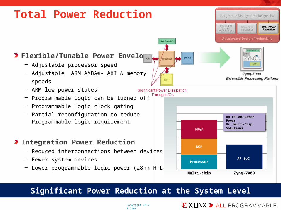
Total Power Reduction
Flexible/Tunable Power Envelope– Adjustable processor speed– Adjustable ARM AMBA®- AXI & memory
speeds– ARM low power states– Programmable logic can be turned off– Programmable logic clock gating– Partial reconfiguration to reduce
Programmable logic requirement
Integration Power Reduction– Reduced interconnections between devices– Fewer system devices– Lower programmable logic power (28nm HPL process)
Multi-chip Zynq-7000
DSP
FPGA
ProcessorAP SoC
Up to 50% Lower PowerVs. Multi-Chip Solutions
Significant Power Reduction at the System Level

Copyright 2012 Xilinx
Accelerated Design Productivity
Reduced Time To Market– Fixed processor system with large set of built in peripherals– Xilinx standardizing on AMBA-4 AXI enhances portability of IPs – Scalable optimized architecture for IP re-use; AXI interfaces for plug & play IP– Accelerate development with targeted design platforms
Increased Time In Market– Software and hardware re-programmability– Field upgradable– Address Processor/ASSPs short shelf life
Dev. Design #1
Platform #1
Dev.
Dev.
Dev.
Design #3
Design #2
Dev. Dev.
ASIC /ASSP /2 Chip
AP SoC
Extended Product life
Platform Approach Enables Horizontal and Vertical Scalability

Copyright 2012 XilinxPage 16
Zynq-7000 AP SoC Applications Mapping

© Copyright 2009 XilinxCopyright 2012 Xilinx
Device Table
Copyright 2012 XilinxPage 18
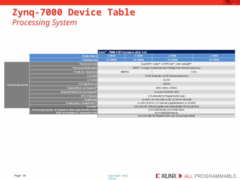
Zynq-7000 Device TableProcessing System
Device Name
Part Number
Processor Core
Processor Extensions
Maximum Frequency
L1 Cache
L2 Cache
On-Chip Memory
External Memory Support(5)
External Static Memory Support(5)
DMA Channels
Peripherals
Peripherals w / built-in DMA(5)
Security(1)
Processing System to Programmable Logic Interface Ports (Primary Interfaces & Interrupts Only)
See next slide for Programmable Logic and package details
XC7Z010 XC7Z020 XC7Z030 XC7Z045
2x AXI 32b Master, 2x AXI 32b Slave,4x AXI 64b/32b Memory
32 KB Instruction, 32 KB Data per processor
512 KB
256 KB
800 MHz 1 GHz
Processing System
2x USB 2.0 (OTG), 2x Tri-mode Gigabit Ethernet, 2x SD/SDIO
AES and SHA 256b Decryption and Authentication for Secure Boot
Z-7010 Z-7020 Z-7030 Z-7045
DDR3, DDR2, LPDDR2
2x Quad-SPI, NAND, NOR
8 (4 dedicated to Programmable Logic)
2x UART, 2x CAN 2.0B, 2x I2C, 2x SPI, 4x 32b GPIO
Zynq™-7000 All Programmable SoC
Dual ARM® Cortex™-A9 MPCore™ w ith CoreSight™
NEON™ & Single / Double Precision Floating Point for each processor

Copyright 2012 XilinxPage 19
Zynq-7000 Device TableProgrammable Logic and Packages
Device Name
Part Number
Xilinx 7 Series Programmable Logic Equivalent
Programmable Logic Cells (Approximate ASIC Gates (3))
Look-Up Tables (LUTs)
Flip-Flops
Extensible Block RAM (# 36 Kb Blocks)
Programmable DSP Slices (18x25 MACCs)
Peak DSP Performance (Symmetric FIR)
PCI Express® (Root Complex or Endpoint)
Agile Mixed Signal (AMS) / XADC(5)
Security(1)
Commercial (0C to 85C)
Extended (0C to 100C)
Industrial (-40C to 100C)
Package Type (4) CLG225(5) CLG400 CLG400 CLG484 FBG484 FBG676 FFG676 FBG676 FFG676 FFG900
Size (mm) 13x13 17x17 17x17 19x19 23x23 27x27 27x27 27x27 27x27 31x31
Pitch (mm) 0.8 0.8 0.8 0.8 1.0 1.0 1.0 1.0 1.0 1.0
Processing System User I/Os (Excludes DDR dedicated I/Os) (2) 32 54 54 54 54 54 54 54 54 54
Multi-Standards and Multi-Voltage SelectIOTM Interfaces(1.2V, 1.35V, 1.5V, 1.8V, 2.5V, 3.3V)
54 100 125 200 100 100 100 100 100 212
Multi-Standards and Multi-Voltage High Performance SelectIO Interfaces
(1.2V, 1.35V, 1.5V, 1.8V)— — — — 63 150 150 150 150 150
Serial Transceivers — — — — 4 4 4 8 8 16
Maximum Transceiver Speed (Speedgrade Dependant) N/A N/A N/A N/A 6.6 Gb/s 6.6 Gb/s 12.5 Gb/s 6.6 Gb/s 12.5 Gb/s 12.5 Gb/s
Notes: 1. Security block is shared by the Processing System and the Programmable Logic.
2. Static memory interface combined w ith the usage of many peripherals could require more than 54 I/Os. In that case the designer can use the Programmable Logic SelectIO interface.
3. Eqivalent ASIC gate count is dependent of the function implemented. The assumption is 1 Logic Cell = ~15 ASIC Gates.
4. Devices in the same package are pin to pin compatible, FBG676 and FFG676 are also pin to pin compatible
5. Z-7010 in CLG225 has restrictions on PS peripherals, Memory interfaces and I/Os. Please refer to the datasheet for more details
6. Preliminary product information. Subject to change. Please contact your Xilinx representative for the latest information
— — Gen2 x4 Gen2 x8
Packages
2x 12 bit, MSPS ADCs w ith up to 17 Differential Inputs
AES and SHA 256b Decryption and Authentication for Secure Programmable Logic Configuration
Speed Grades
-1
-2, -3
-1, -2
Programmable Logic
Artix™-7 FPGA
80 220 400 900
100 GMACS 276 GMACS 593 GMACS 1334 GMACS
218,600
240 KB (60) 560 KB (140) 1,060 KB (265) 2,180 KB (545)
35,200 106,400 157,200 437,200
17,600 53,200 78,600
Artix™-7 FPGA Kintex™-7 FPGA Kintex™-7 FPGA
28K Logic Cells (~430K) 85K Logic Cells (~1.3M) 125K Logic Cells (~1.9M) 350K Logic Cells (~5.2M)
XC7Z010 XC7Z020 XC7Z030 XC7Z045
Zynq™-7000 All Programmable SoCZ-7010 Z-7020 Z-7030 Z-7045