© s.n. sabki revision chapter 9 chapter 9 part ii
TRANSCRIPT

© S.N. Sabki
Revision Revision CHAPTER 9CHAPTER 9
Part IIPart II
© S.N. Sabki
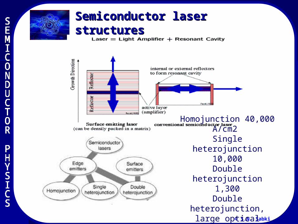
Semiconductor laser Semiconductor laser structuresstructures
Homojunction 40,000 A/cm2
Single heterojunction 10,000
Double heterojunction 1,300
Double heterojunction, large optical cavity
600
© S.N. Sabki
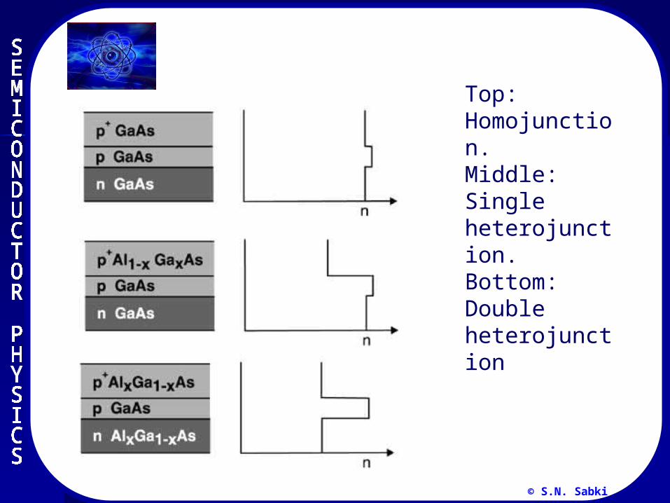
Top: Homojunction. Middle: Single heterojunction. Bottom: Double heterojunction
© S.N. Sabki
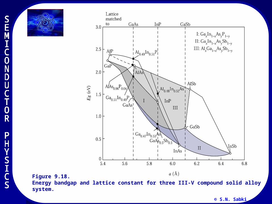
Figure 9.18. Energy bandgap and lattice constant for three III-V compound solid alloy system.
© S.N. Sabki
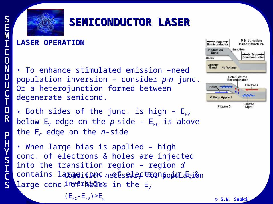
LASER OPERATION
• To enhance stimulated emission –need population inversion – consider p-n junc. Or a heterojunction formed between degenerate semicond.
• Both sides of the junc. is high – EFV below EV edge on the p-side – EFC is above the EC edge on the n-side
• When large bias is applied – high conc. of electrons & holes are injected into the transition region – region d contains large conc. of electrons in EC & large conc. of holes in the EV
Condition necessary for population inversion:
(EFC-EFV)>Eg
SEMICONDUCTOR LASERSEMICONDUCTOR LASER
© S.N. Sabki
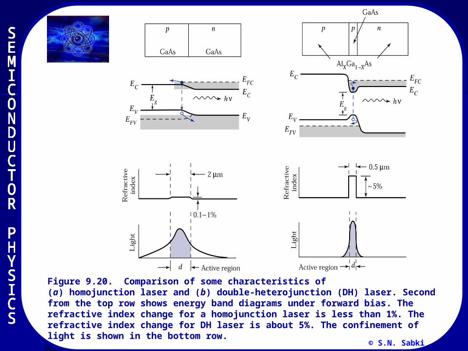
Figure 9.20. Comparison of some characteristics of (a) homojunction laser and (b) double-heterojunction (DH) laser. Second from the top row shows energy band diagrams under forward bias. The refractive index change for a homojunction laser is less than 1%. The refractive index change for DH laser is about 5%. The confinement of light is shown in the bottom row.
© S.N. Sabki
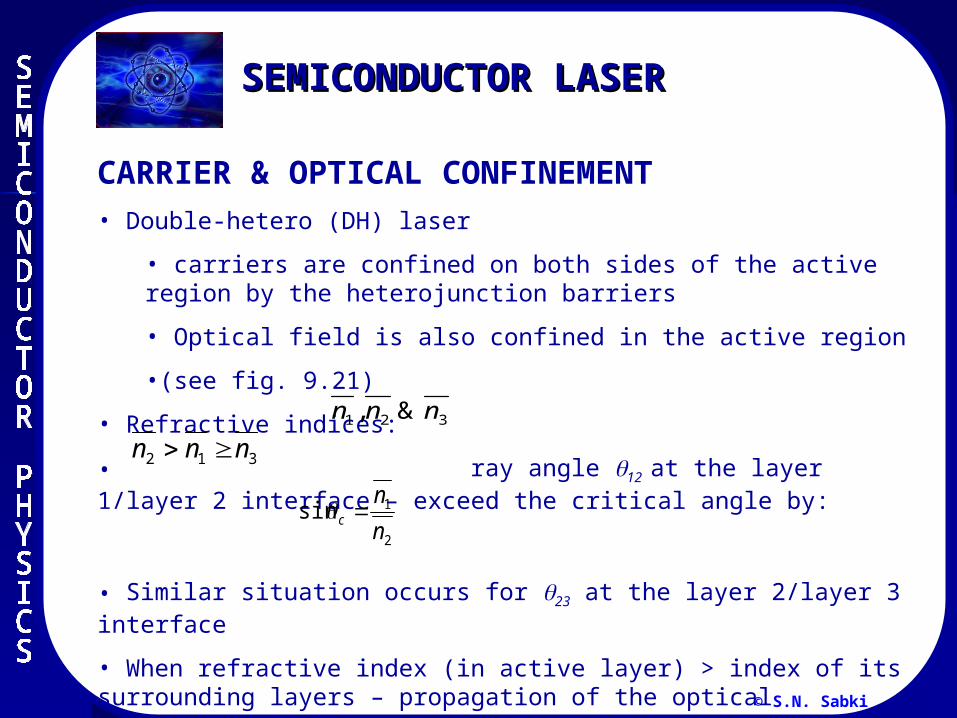
CARRIER & OPTICAL CONFINEMENT• Double-hetero (DH) laser
• carriers are confined on both sides of the active region by the heterojunction barriers
• Optical field is also confined in the active region
•(see fig. 9.21)
• Refractive indices:
• ray angle 12 at the layer 1/layer 2 interface – exceed the critical angle by:
• Similar situation occurs for 23 at the layer 2/layer 3 interface
• When refractive index (in active layer) > index of its surrounding layers – propagation of the optical radiation is confined in a direction parallel to the layer interfaces
321 &, nnn
312 nnn
2
1sinn
nc
SEMICONDUCTOR LASERSEMICONDUCTOR LASER
© S.N. Sabki
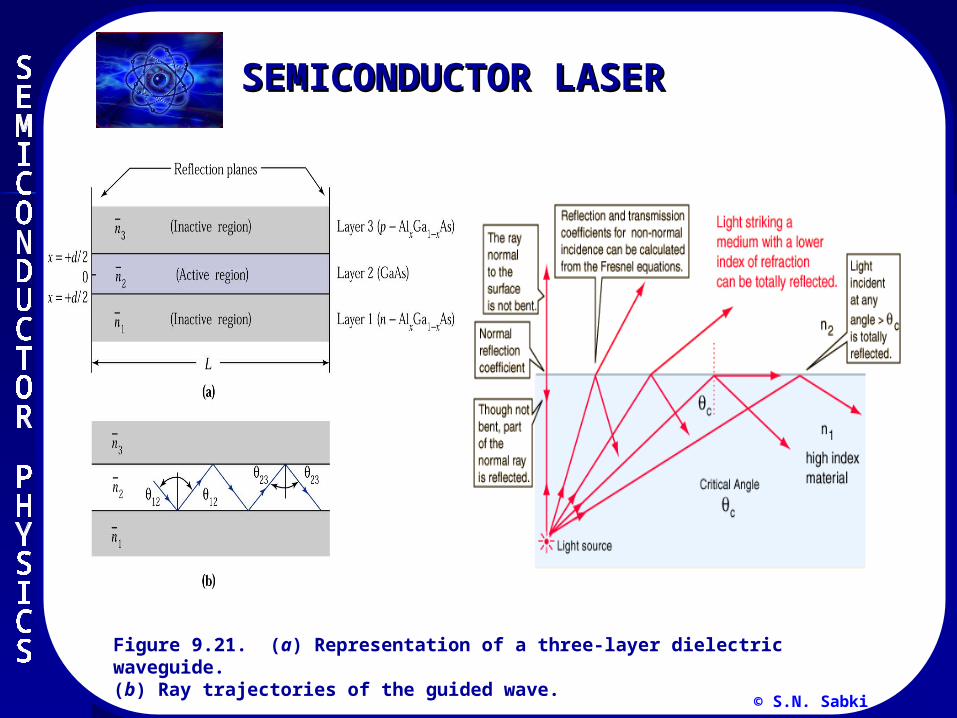
Figure 9.21. (a) Representation of a three-layer dielectric waveguide. (b) Ray trajectories of the guided wave.
SEMICONDUCTOR LASERSEMICONDUCTOR LASER
© S.N. Sabki
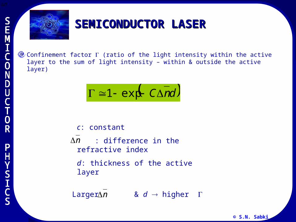
Confinement factor (ratio of the light intensity within the active layer to the sum of light intensity – within & outside the active layer)
dnC exp1
c: constant
: difference in the refractive index
d: thickness of the active layer
n
n
Larger & d higher n
SEMICONDUCTOR LASERSEMICONDUCTOR LASER
© S.N. Sabki
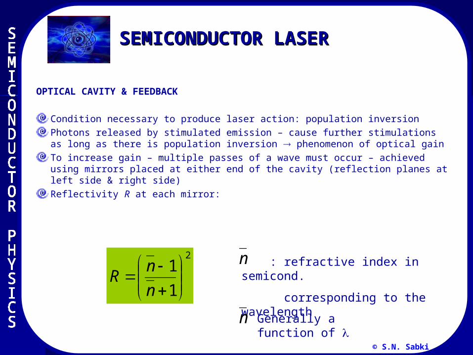
OPTICAL CAVITY & FEEDBACK
Condition necessary to produce laser action: population inversion
Photons released by stimulated emission – cause further stimulations as long as there is population inversion phenomenon of optical gain
To increase gain – multiple passes of a wave must occur – achieved using mirrors placed at either end of the cavity (reflection planes at left side & right side)
Reflectivity R at each mirror:
2
1
1
n
nR
: refractive index in semicond.
corresponding to the wavelength
n
n Generally a function of
SEMICONDUCTOR LASERSEMICONDUCTOR LASER
© S.N. Sabki
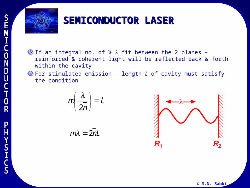
If an integral no. of ½ fit between the 2 planes – reinforced & coherent light will be reflected back & forth within the cavity
For stimulated emission – length L of cavity must satisfy the condition
Ln
m
2
Lnm 2
m: integral number
SEMICONDUCTOR LASERSEMICONDUCTOR LASER
© S.N. Sabki
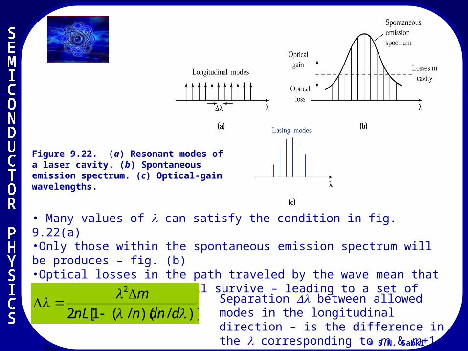
• Many values of can satisfy the condition in fig. 9.22(a)•Only those within the spontaneous emission spectrum will be produces – fig. (b)•Optical losses in the path traveled by the wave mean that only strongest lines will survive – leading to a set of lasing modes – fig. (c)
)]/)(/(1[2
2
ddnnnL
m
Separation between allowed modes in the longitudinal direction – is the difference in the corresponding to m & m+1
Figure 9.22. (a) Resonant modes of a laser cavity. (b) Spontaneous emission spectrum. (c) Optical-gain wavelengths.
© S.N. Sabki
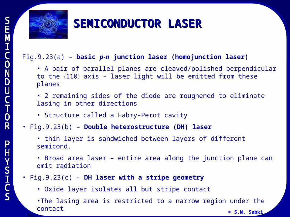
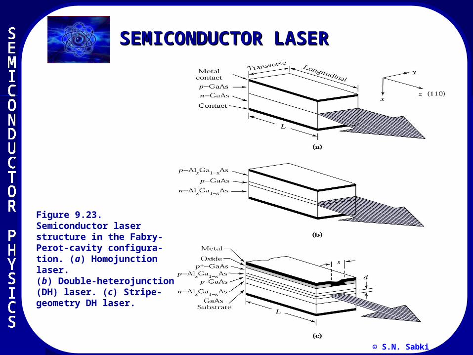
Fig.9.23(a) – basic p-n junction laser (homojunction laser)
• A pair of parallel planes are cleaved/polished perpendicular to the 110 axis – laser light will be emitted from these planes
• 2 remaining sides of the diode are roughened to eliminate lasing in other directions
• Structure called a Fabry-Perot cavity
• Fig.9.23(b) – Double heterostructure (DH) laser
• thin layer is sandwiched between layers of different semicond.
• Broad area laser – entire area along the junction plane can emit radiation
• Fig.9.23(c) - DH laser with a stripe geometry
• Oxide layer isolates all but stripe contact
•The lasing area is restricted to a narrow region under the contact
• Advantages of stripe geometry – reduced operating current, elimination of multiple emission areas along the junction & improved reliability
SEMICONDUCTOR LASERSEMICONDUCTOR LASER
© S.N. Sabki
Figure 9.23. Semiconductor laser structure in the Fabry-Perot-cavity configura-tion. (a) Homojunction laser. (b) Double-heterojunction (DH) laser. (c) Stripe-geometry DH laser.
SEMICONDUCTOR LASERSEMICONDUCTOR LASER
© S.N. Sabki
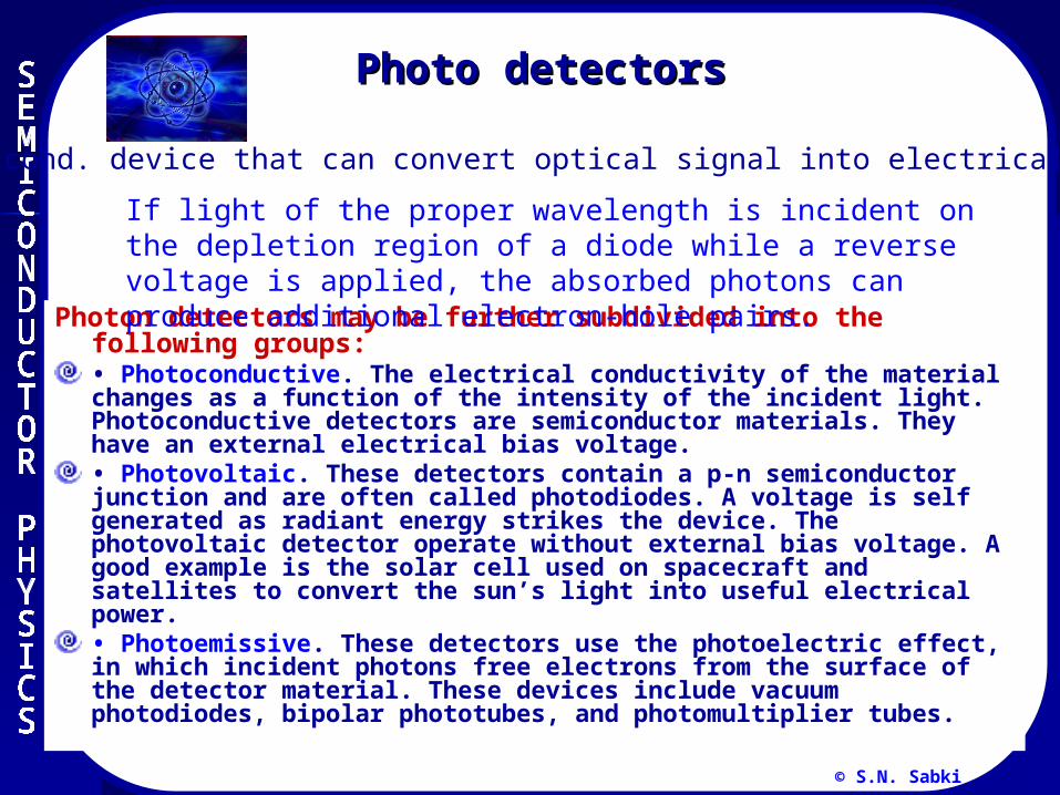
Photo detectors Photo detectors
Photon detectors may be further subdivided into the following groups:• Photoconductive. The electrical conductivity of the material changes as a function of the intensity of the incident light. Photoconductive detectors are semiconductor materials. They have an external electrical bias voltage.• Photovoltaic. These detectors contain a p-n semiconductor junction and are often called photodiodes. A voltage is self generated as radiant energy strikes the device. The photovoltaic detector operate without external bias voltage. A good example is the solar cell used on spacecraft and satellites to convert the sun’s light into useful electrical power.• Photoemissive. These detectors use the photoelectric effect, in which incident photons free electrons from the surface of the detector material. These devices include vacuum photodiodes, bipolar phototubes, and photomultiplier tubes.
If light of the proper wavelength is incident on the depletion region of a diode while a reverse voltage is applied, the absorbed photons can produce additional electron-hole pairs.
Semicond. device that can convert optical signal into electrical signal
© S.N. Sabki
When incident light falls on the surface of photoconductor – electron-hole pairs are generated – conductivity increased
• For intrinsic photoconductor - Increasing of conductivity under illumination – due to the increase in the no. of carriers
• For extrinsic photoconductor – photoexcitation may occur between the band edge & energy level in the Eg
•Photocurrent between electrodes: Primary photocurrent:
L
E
hv
PqI nopt
p
hv
PqI opt
ph
r
n
ph
p
tL
E
I
I Gain
Photocurrent gain:
: quantum efficiency
Popt:incident optical power
hv: photon energy
: carrier lifetime
E: electric field
= carrier transit time
PHOTOCONDUCTORPHOTOCONDUCTOR
© S.N. Sabki
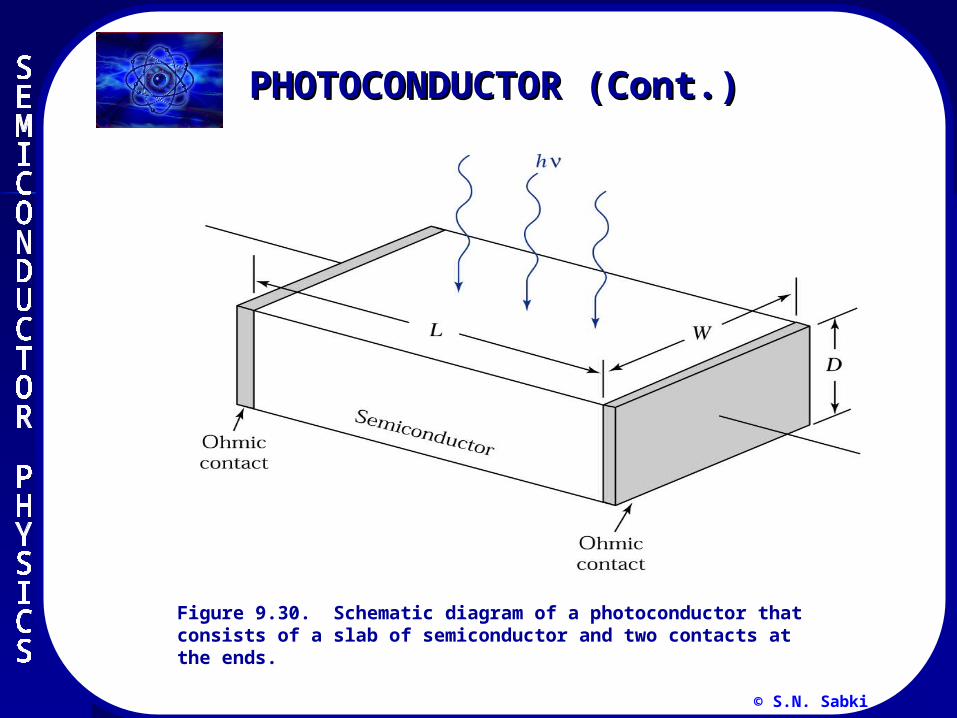
Figure 9.30. Schematic diagram of a photoconductor that consists of a slab of semiconductor and two contacts at the ends.
PHOTOCONDUCTOR (Cont.)PHOTOCONDUCTOR (Cont.)
© S.N. Sabki
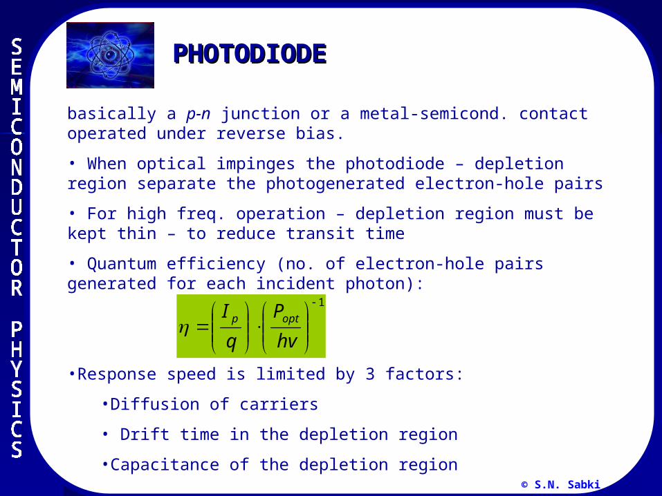
basically a p-n junction or a metal-semicond. contact operated under reverse bias.
• When optical impinges the photodiode – depletion region separate the photogenerated electron-hole pairs
• For high freq. operation – depletion region must be kept thin – to reduce transit time
• Quantum efficiency (no. of electron-hole pairs generated for each incident photon):
•Response speed is limited by 3 factors:
•Diffusion of carriers
• Drift time in the depletion region
•Capacitance of the depletion region
1
hv
P
q
I optp
PHOTODIODE PHOTODIODE
© S.N. Sabki
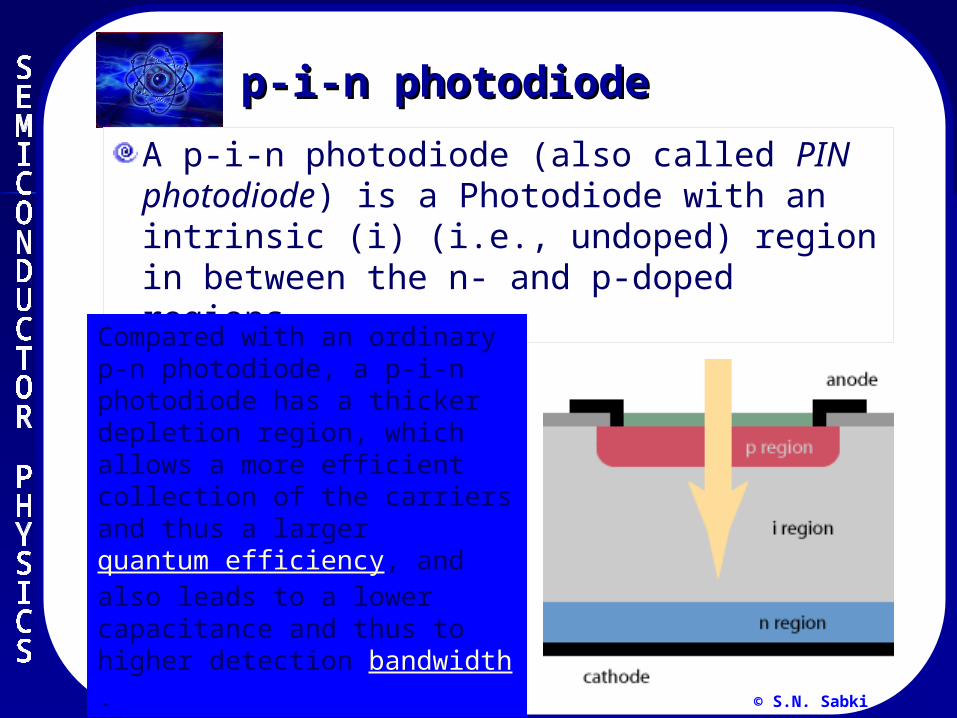
p-i-n photodiodep-i-n photodiode
A p-i-n photodiode (also called PIN photodiode) is a Photodiode with an intrinsic (i) (i.e., undoped) region in between the n- and p-doped regions.
Compared with an ordinary p-n photodiode, a p-i-n photodiode has a thicker depletion region, which allows a more efficient collection of the carriers and thus a larger quantum efficiency, and also leads to a lower capacitance and thus to higher detection bandwidth.
© S.N. Sabki
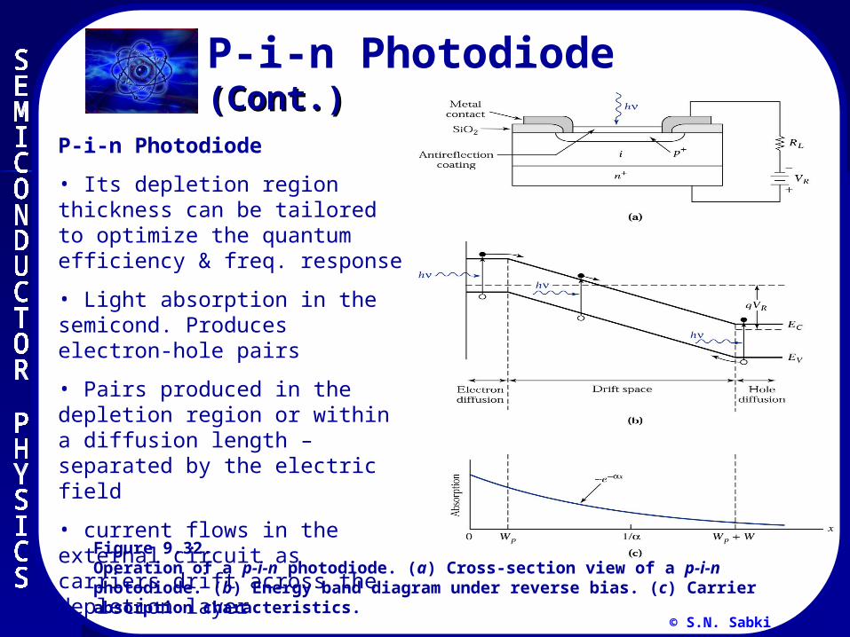
Figure 9.32. Operation of a p-i-n photodiode. (a) Cross-section view of a p-i-n photodiode. (b) Energy band diagram under reverse bias. (c) Carrier absorption characteristics.
P-i-n Photodiode
• Its depletion region thickness can be tailored to optimize the quantum efficiency & freq. response
• Light absorption in the semicond. Produces electron-hole pairs
• Pairs produced in the depletion region or within a diffusion length – separated by the electric field
• current flows in the external circuit as carriers drift across the depletion layer
P-i-n Photodiode (Cont.) (Cont.)
© S.N. Sabki
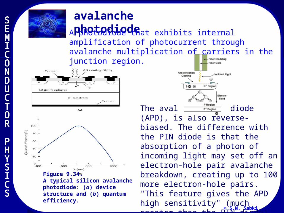
Figure 9.34. A typical silicon avalanche photodiode: (a) device structure and (b) quantum efficiency.
avalanche photodiode
The avalanche photodiode (APD), is also reverse-biased. The difference with the PIN diode is that the absorption of a photon of incoming light may set off an electron-hole pair avalanche breakdown, creating up to 100 more electron-hole pairs. "This feature gives the APD high sensitivity" (much greater than the PIN diode).
A photodiode that exhibits internal amplification of photocurrent through avalanche multiplication of carriers in the junction region.
© S.N. Sabki
•Advantages:
•Can convert sunlight directly to electricity with good conversion efficiency
•Provide nearly permanent power at low operating cost
•Non polluting
SOLAR CELLSOLAR CELL
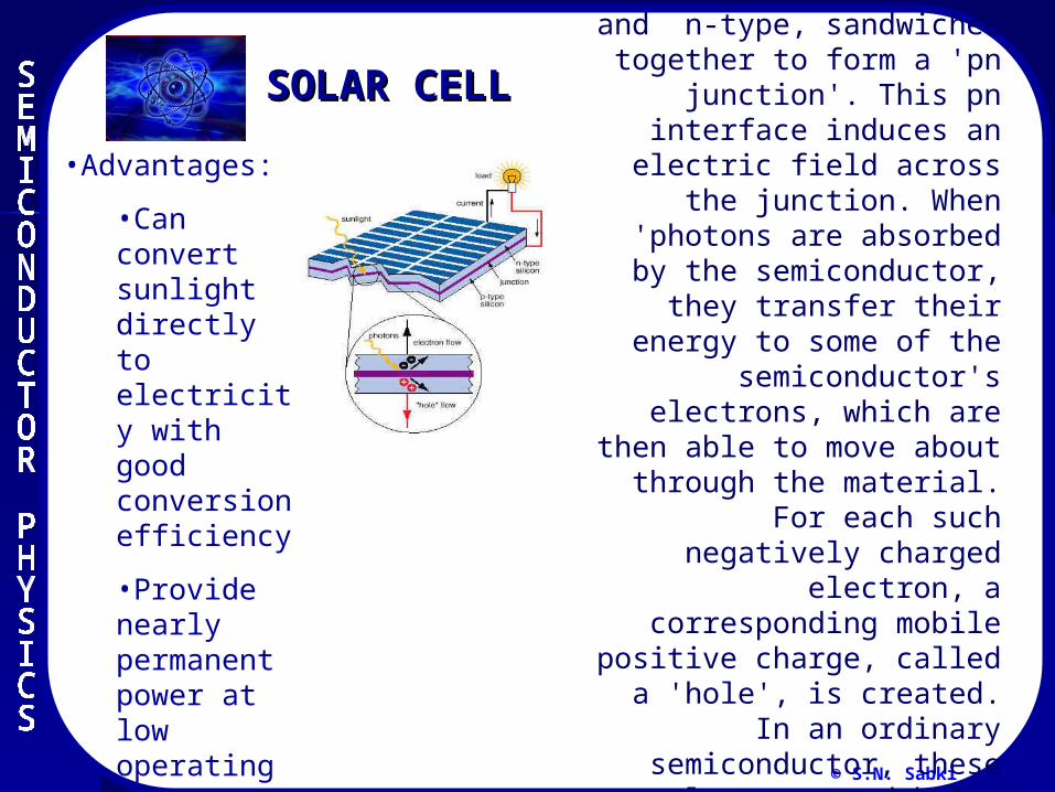
A solar cell consists of two layers of semiconductor, p-
type and n-type, sandwiched together to
form a 'pn junction'. This pn interface induces an electric
field across the junction. When 'photons are
absorbed by the semiconductor, they
transfer their energy to some of the
semiconductor's electrons, which are then able to
move about through the material. For each such
negatively charged electron, a corresponding
mobile positive charge, called a 'hole', is created. In an ordinary semiconductor,
these electrons and holes recombine after a short time and their energy is
wasted as heat.