01 asic design flow
DESCRIPTION
áicTRANSCRIPT

12/201212/2012 1
ASIC Design Flow TS. Hoang Trang ThS. Pham Dang Lam
12/201212/2012 2
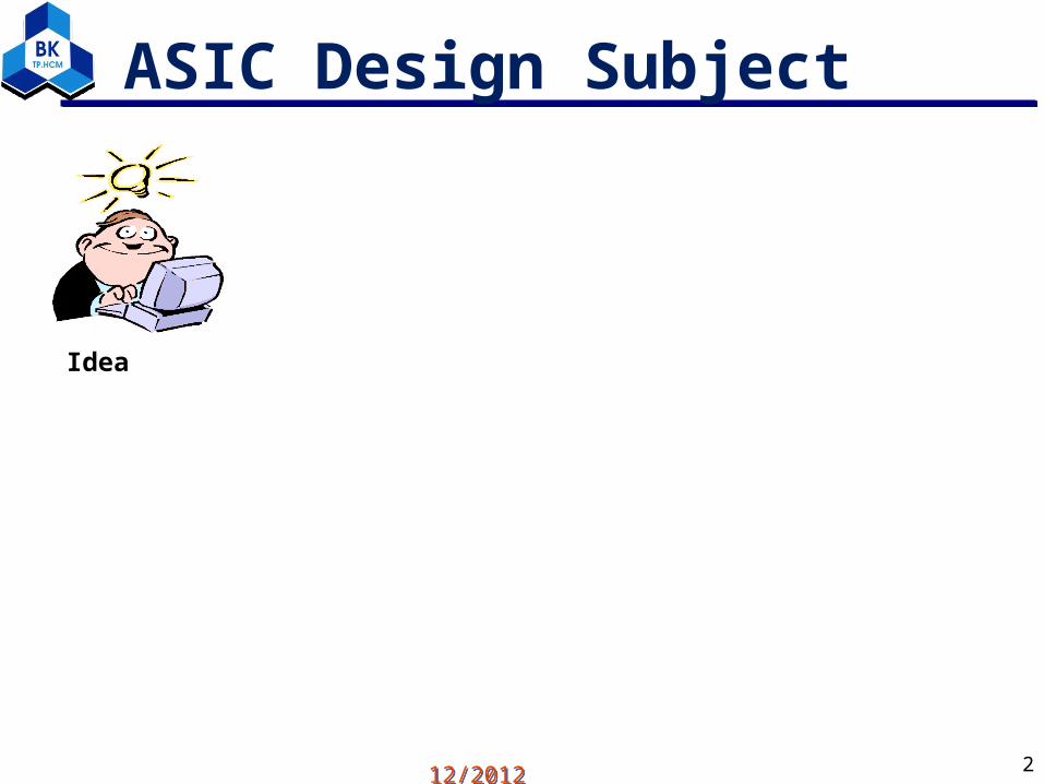
ASIC Design Subject
Idea

12/201212/2012 3
ASIC Design Subject
Hardware Develop
Idea
12/201212/2012 4
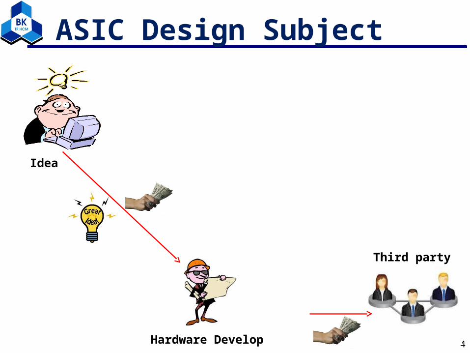
ASIC Design Subject
Hardware Develop
Idea
Third party

12/201212/2012 5
ASIC Design Subject
Hardware Develop
Third party
Idea

12/201212/2012 6
ASIC Design Subject
Layout
Factory
Hardware Develop
Third party
Idea
12/201212/2012 7
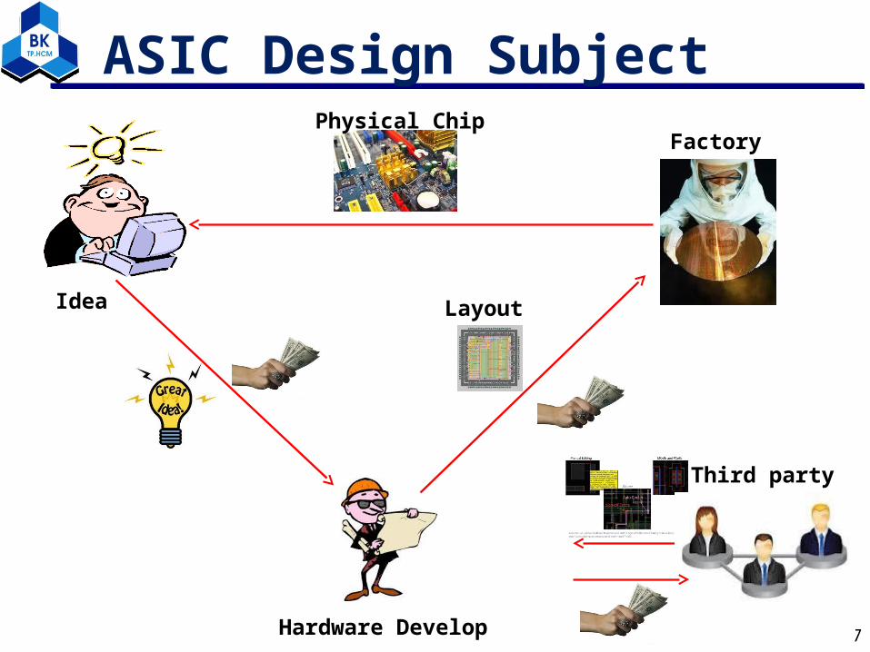
ASIC Design Subject
Layout
Physical ChipFactory
Hardware Develop
Third party
Idea

12/201212/2012 8
ASIC Design Subject
Layout
Physical ChipFactory
Hardware Develop
Third party
Idea
12/201212/2012 9
ASIC Design Subject
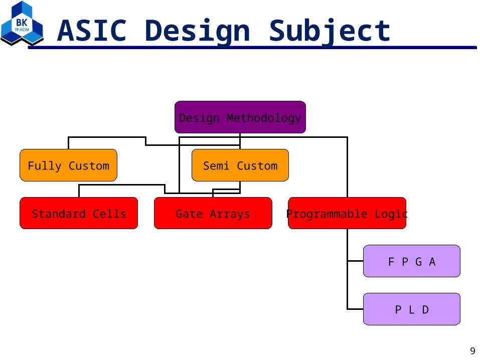
Design Methodology
Fully Custom Semi Custom
Standard Cells Gate Arrays Programmable Logic
F P G A
P L D

12/201212/2012 10
ASIC Design Subject
Design Methodology
Fully Custom Semi Custom
Standard Cells Gate Arrays Programmable Logic
F P G A
P L D
ASIC Design Flow(Application-specific integrated circuit)
FPGA Design Flow(Field Programmable Gate Array)

12/201212/2012 11
ASIC Design Subject
•Use predesigned, pretested and pre_characterized logic cells from the standards-cell library as building blocks.
•The chip layout is customized
•Advantages: Save design time and money, reduce risk compared to full-custom design
•Disadvantages: Still incurs high none-recurring-engineering (NRE) cost and long manufacture time
•Design a chip from scratch
•Engineer design some or all the logic cells, circuits, and the chip layout specifically for a full-custom IC
•Advantages: Complete flexibility, high degree of optimization performance ad area
•Disadvantages: Large amount of design effort, expensive
Full Custom Standard Cell Base
•Parts of the chip are pre-fabricated, and other parts are custom fabricated for particular customer’s circuit.
•Idential base cells are pre-fabricated in the form of a 2-D array on a gate-array (this partially finished chip is called gate-array template).
•This wires between the transistors inside the cells and between the cells are custom fabricated for each customer
•Custom mask are made for the wiring only
Gate Array
•A PLD is a general-purpose chip for implementing logic circuitry.
•Transistors and wires are already prefebricated on a PLD
•Logic cells and interconnect can be programmed by end-user to implement specific circuitry
•No need to create custom masks for each customer
PLD

12/201212/2012 12
ASIC Design Subject
Design
Manufacturing
Packaging/Test
Fabrication/Test
Mask Production
ASIC Design Flow
Hardware Development Activities
Shipping
Back end Process
Front end Process(Wafer Process)
Back end Design
Front end Design
GDS

12/201212/2012 13
ASIC Design Subject
Product
Hardware
Software
Middleware
Device driver
Compiler, OS
Board, Hardware Flatform
SemiconductorDevice
Discrete Device
IntegratedDevice
LedBJTDiodeFET
DigitalAnalogMix Signal
Develop & Evaluate Design Kit

12/201212/2012 14
ASIC Design Subject
Product
Hardware
Software
Middleware
Device driver
Compiler, OS
Board, Hardware Flatform
SemiconductorDevice
Discrete Device
IntegratedDevice
LedBJTDiodeFET
DigitalAnalogMix Signal
Develop & Evaluate Design Kit
12/201212/2012 15
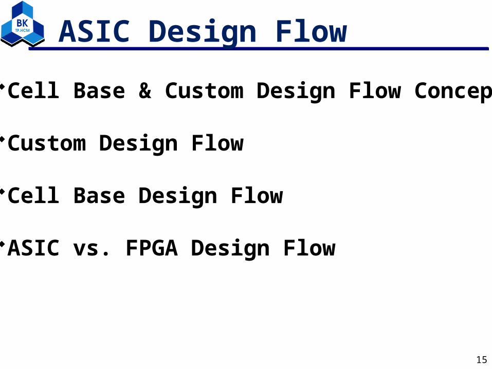
ASIC Design Flow
Cell Base & Custom Design Flow Concepts
Custom Design Flow
Cell Base Design Flow
ASIC vs. FPGA Design Flow

12/201212/2012 16
ASIC Design Flow
Cell Base & Custom Design Flow Concepts
Custom Design Flow
Cell Base Design Flow
ASIC vs. FPGA Design Flow
12/201212/2012 17
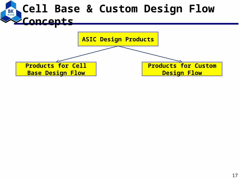
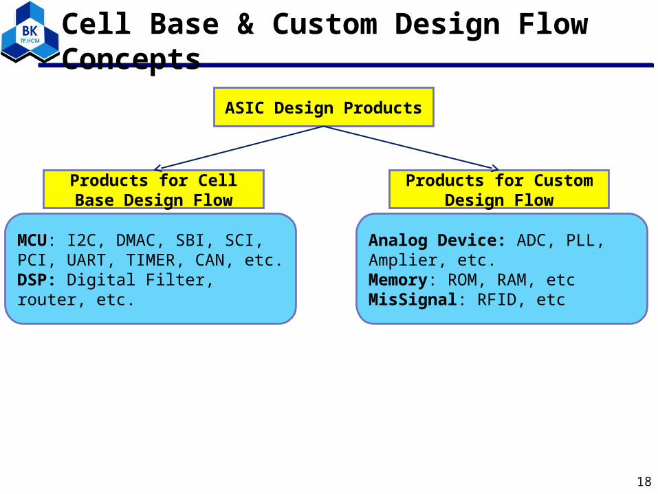
ASIC Design Products
Products for Cell Base Design Flow
Products for Custom Design Flow
Cell Base & Custom Design Flow Concepts
12/201212/2012 18
ASIC Design Products
Products for Cell Base Design Flow
Products for Custom Design Flow
MCU: I2C, DMAC, SBI, SCI, PCI, UART, TIMER, CAN, etc.DSP: Digital Filter, router, etc.
Analog Device: ADC, PLL, Amplier, etc.Memory: ROM, RAM, etcMisSignal: RFID, etc
Cell Base & Custom Design Flow Concepts

12/201212/2012
Custom Design Flow
19
Cell Base & Custom Design Flow Concepts

12/201212/2012
Custom Design Flow
20
Cell Base & Custom Design Flow Concepts

12/201212/2012
Custom Design Flow
21
CMOS Level
Cell Base & Custom Design Flow Concepts

12/201212/2012
Custom Design Flow
22
Symbol Level
CMOS Level
Cell Base & Custom Design Flow Concepts
12/201212/2012
Custom Design Flow
23
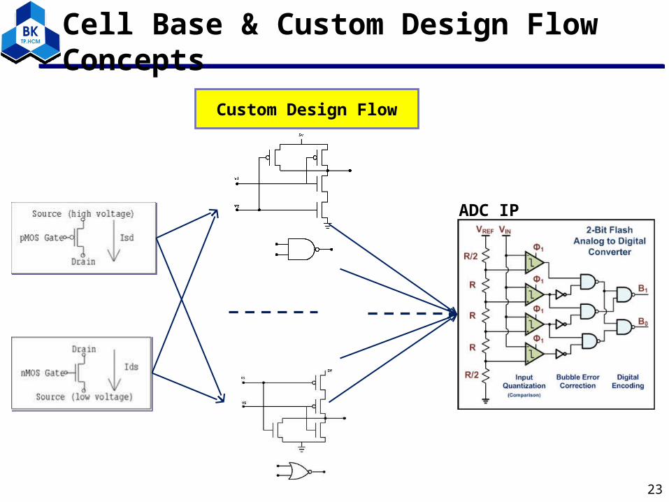
ADC IP
Cell Base & Custom Design Flow Concepts

12/201212/2012
Build Library
from the scratch
Custom Design Flow
24
ADC IP
Cell Base & Custom Design Flow Concepts
12/201212/2012
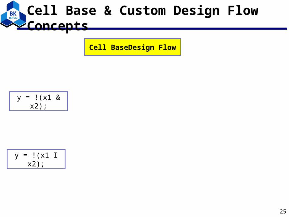
Cell BaseDesign Flow
y = !(x1 & x2);
y = !(x1 I x2);
25
Cell Base & Custom Design Flow Concepts

12/201212/2012
Cell BaseDesign Flow
y = !(x1 & x2);
y = !(x1 I x2);
26
RTL Level
Cell Base & Custom Design Flow Concepts

12/201212/2012
Cell BaseDesign Flow
y = !(x1 & x2);
y = !(x1 I x2);
matching
matching
27
Cell Base & Custom Design Flow Concepts

12/201212/2012
Cell BaseDesign Flow
y = !(x1 & x2);
y = !(x1 I x2); matching
28
UART IPmatching
Cell Base & Custom Design Flow Concepts

12/201212/2012
Ready Library
Cell BaseDesign Flow
y = !(x1 & x2);
y = !(x1 I x2);
matching
matching
29
UART IP
Cell Base & Custom Design Flow Concepts

12/201212/2012
•Use predesigned, pretested and pre_characterized logic cells from the standards-cell library as building blocks.
•The chip layout is customized
•Advantages: Save design time and money, reduce risk compared to full-custom design
•Disadvantages: Still incurs high none-recurring-engineering (NRE) cost and long manufacture time
30
ASIC Design Flows
Cell Base Design Flow Custom Design Flow
•Design a chip from scratch
•Engineer design some or all the logic cells, circuits, and the chip layout specifically for a full-custom IC
•Advantages: Complete flexibility, high degree of optimization performance ad area
•Disadvantages: Large amount of design effort, expensive
Cell Base & Custom Design Flow Concepts
12/201212/2012 31
comparision Cell Base Design Custom Design
Integration Density
X
Speech X
Chip Scale X
Support Tools X
Time to market X
Risk reduction X
http://www.ami.ac.uk/courses/ami4407_dicdes/u03/#3.2http://www.eng.uwo.ca/people/wwang/ece616a/616_extra/notes_web/1_dintro.pdfhttp://www.ece.ucdavis.edu/~bbaas/116/notes/Handout.std.cell.design.pdf
Cell Base & Custom Design Flow Concepts

12/201212/2012 32
ASIC Design Flow
Cell Base & Custom Design Flow Concepts
Custom Design Flow
Cell Base Design Flow
ASIC vs. FPGA Design Flow

12/201212/2012
Custom Design Flow
33
Design flow Support Tools Output

12/201212/2012 34
Specifications
Design flow Support Tools Output
<file>.docx/xls/ppt
Custom Design Flow

12/201212/2012 35
Specifications
Schematic
Design flow Support Tools
Composer
Output
<file>.docx/xls/ppt
Custom Design Flow

12/201212/2012 36
Specifications
Schematic
Netlist extractionNG
Design flow Support Tools
Composer
Composer
Output
<file>.docx/xls/ppt
<file>.cdl, <file>.net
Custom Design Flow
12/201212/2012 37
Specifications
Schematic
Pre_Layout Verification
Netlist extractionNG
Design flow Support Tools
Composer
Composer
HSpice
Output
<file>.docx/xls/ppt
<file>.cdl, <file>.net
<file>.wf, <file>.tr
Custom Design Flow

12/201212/2012 38
Specifications
Schematic
Pre_Layout Verification
Layout
Netlist extractionNG
Design flow Support Tools
Composer
Composer
HSpice
Virtuoso
Output
<file>.docx/xls/ppt
<file>.cdl, <file>.net
<file>.wf, <file>.tr
<file>.gds
Custom Design Flow

12/201212/2012 39
Specifications
Schematic
Pre_Layout Verification
Layout
Layout Verification
Netlist extractionNG
Design flow Support Tools
Composer
Composer
HSpice
Virtuoso
Calibre
Output
<file>.docx/xls/ppt
<file>.cdl, <file>.net
<file>.wf, <file>.tr
<file>.gds
<file>.db (DRC) <file>.svdb(LVS)
NG
DRC: Design Rule CheckLVS: Layout Versus Schematic
Custom Design Flow
12/201212/2012 40
Specifications
Schematic
Pre_Layout Verification
Layout
Layout Verification
RC_extraction
Pos_LayoutVerification
Netlist extractionNG
Design flow Support Tools
Composer
Composer
HSpice
Virtuoso
Calibre
Output
<file>.docx/xls/ppt
<file>.cdl, <file>.net
<file>.wf, <file>.tr
<file>.gds
<file>.db (DRC) <file>.svdb(LVS)
NG
DRC: Design Rule CheckLVS: Layout Versus Schematic
Spectre SimulatorPritime
Report file<file>.lib/.db
Custom Design Flow

12/201212/2012 41
ASIC Design Flow
Cell Base & Custom Design Flow Concepts
Custom Design Flow
Cell Base Design Flow
ASIC vs. FPGA Design Flow

12/201212/2012 42
Design flowSupport Tools (Languages)
Output
Cell Base Design Flow

12/201212/2012 43
Specifications
Design flowSupport Tools (Languages)
Output
<file>.docx/xls/ppt
Cell Base Design Flow

12/201212/2012 44
Specifications
Design flowSupport Tools (Languages)
Output
<file>.docx/xls/ppt
Cell Base Design Flow
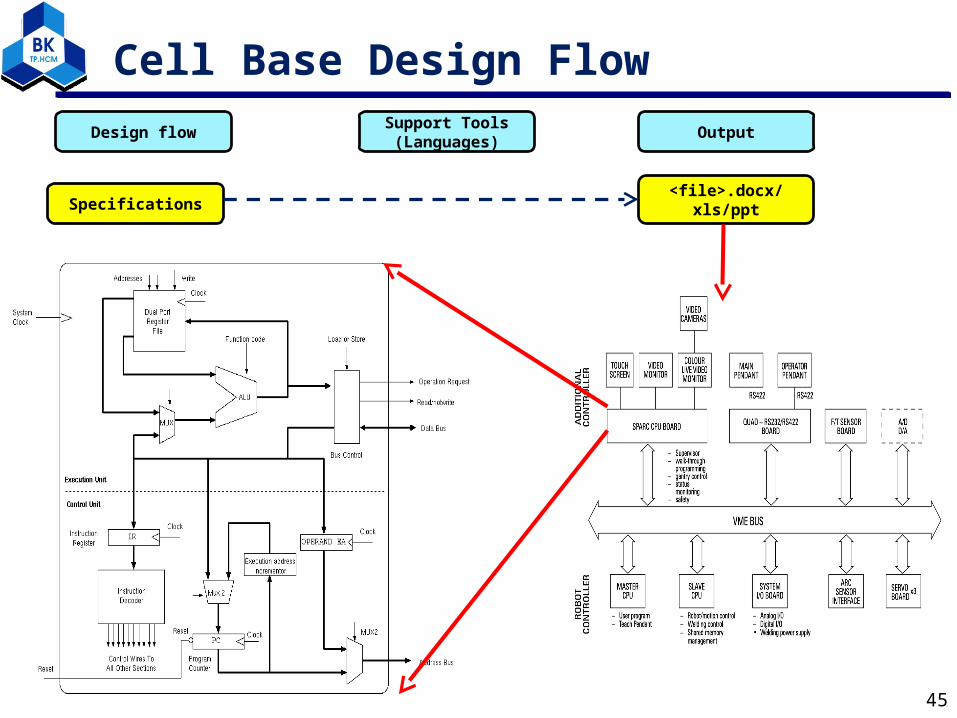
12/201212/2012 45
Specifications
Design flowSupport Tools (Languages)
Output
<file>.docx/xls/ppt
Cell Base Design Flow
12/201212/2012 46
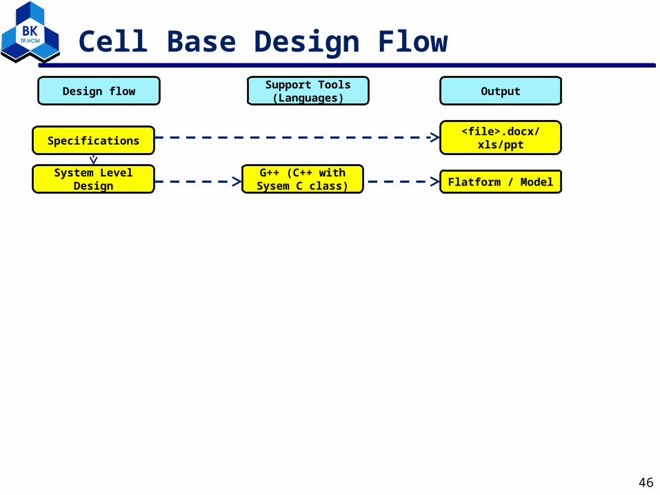
Specifications
System Level Design
Design flowSupport Tools (Languages)
Output
<file>.docx/xls/ppt
Flatform / ModelG++ (C++ with
Sysem C class)
Cell Base Design Flow

12/201212/2012 47
Specifications
System Level Design
RTL Design
Design flowSupport Tools (Languages)
VI, NotePath++ (Verilog/VHDL)
Output
<file>.docx/xls/ppt
<file>.v
Flatform / ModelG++ (C++ with
Sysem C class)
Cell Base Design Flow

12/201212/2012 48
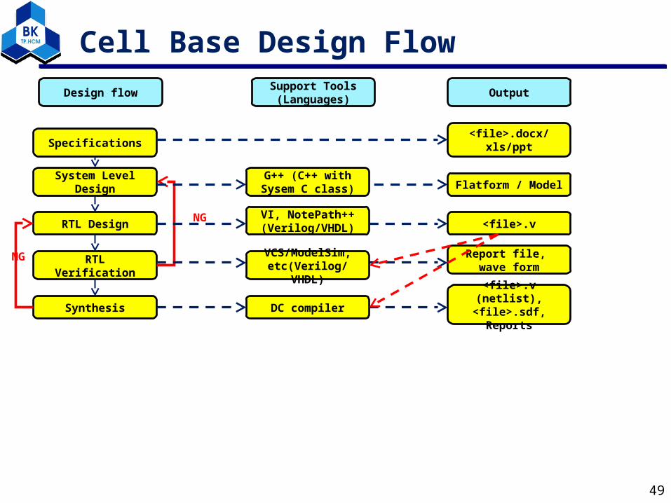
Specifications
System Level Design
RTL Verification
RTL DesignNG
Design flowSupport Tools (Languages)
VI, NotePath++ (Verilog/VHDL)
Output
<file>.docx/xls/ppt
<file>.v
Report file, wave form
VCS/ModelSim, etc(Verilog/ VHDL)
Flatform / ModelG++ (C++ with
Sysem C class)
Cell Base Design Flow
12/201212/2012 49
Specifications
System Level Design
RTL Verification
Synthesis
RTL DesignNG
Design flowSupport Tools (Languages)
VI, NotePath++ (Verilog/VHDL)
DC compiler
Output
<file>.docx/xls/ppt
<file>.v
Report file, wave form
<file>.v (netlist), <file>.sdf,Reports
VCS/ModelSim, etc(Verilog/ VHDL)
Flatform / ModelG++ (C++ with
Sysem C class)
NG
Cell Base Design Flow

12/201212/2012 50
Specifications
System Level Design
RTL Verification
Synthesis
Netlist Verification
RTL DesignNG
Design flowSupport Tools (Languages)
VI, NotePath++ (Verilog/VHDL)
DC compiler
Formality
Output
<file>.docx/xls/ppt
<file>.v
Report file, wave form
<file>.v (netlist), <file>.sdf,Reports
Report file
NG
VCS/ModelSim, etc(Verilog/ VHDL)
Flatform / ModelG++ (C++ with
Sysem C class)
NG
Cell Base Design Flow
12/201212/2012 51
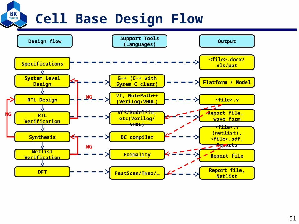
Specifications
System Level Design
RTL Verification
Synthesis
Netlist Verification
DFT
RTL DesignNG
Design flowSupport Tools (Languages)
VI, NotePath++ (Verilog/VHDL)
DC compiler
Formality
Output
<file>.docx/xls/ppt
<file>.v
Report file, wave form
<file>.v (netlist), <file>.sdf,Reports
Report file
NG
VCS/ModelSim, etc(Verilog/ VHDL)
FastScan/Tmax/… Report file, Netlist
Flatform / ModelG++ (C++ with
Sysem C class)
NG
Cell Base Design Flow

12/201212/2012 52
Specifications
System Level Design
RTL Verification
Synthesis
Netlist Verification
DFT
STA
RTL DesignNG
Design flowSupport Tools (Languages)
VI, NotePath++ (Verilog/VHDL)
DC compiler
Formality
Output
<file>.docx/xls/ppt
<file>.v
Report file, wave form
<file>.v (netlist), <file>.sdf,Reports
Report file
NG
Prime Time Report file, Netlist
VCS/ModelSim, etc(Verilog/ VHDL)
FastScan/Tmax/… Report file, Netlist
Flatform / ModelG++ (C++ with
Sysem C class)
NG
Cell Base Design Flow

12/201212/2012 53
Specifications
System Level Design
RTL Verification
Synthesis
Netlist Verification
DFT
STA
RTL DesignNG
Design flowSupport Tools (Languages)
VI, NotePath++ (Verilog/VHDL)
DC compiler
Formality
Output
<file>.docx/xls/ppt
<file>.v
Report file, wave form
<file>.v (netlist), <file>.sdf,Reports
Report file
NG
Prime Time Report file, Netlist
VCS/ModelSim, etc(Verilog/ VHDL)
ICC compiler <file>.gdsPlace&Route
FastScan/Tmax/… Report file, Netlist
Flatform / ModelG++ (C++ with
Sysem C class)
NG
Cell Base Design Flow

12/201212/2012 54
Specifications
System Level Design
RTL Verification
Synthesis
Netlist Verification
DFT
STA
RTL DesignNG
Design flowSupport Tools (Languages)
VI, NotePath++ (Verilog/VHDL)
DC compiler
Formality
Output
<file>.docx/xls/ppt
<file>.v
Report file, wave form
<file>.v (netlist), <file>.sdf,Reports
Report file
NG
Prime Time Report file, Netlist
VCS/ModelSim, etc(Verilog/ VHDL)
ICC compiler <file>.gdsPlace&Route
FastScan/Tmax/… Report file, Netlist
Flatform / ModelG++ (C++ with
Sysem C class)
NG
FrontEnd
BackEnd
Cell Base Design Flow
12/201212/2012 55
Specifications
Design flowSupport Tools (Languages)
Output
<file>.docx/xls/ppt
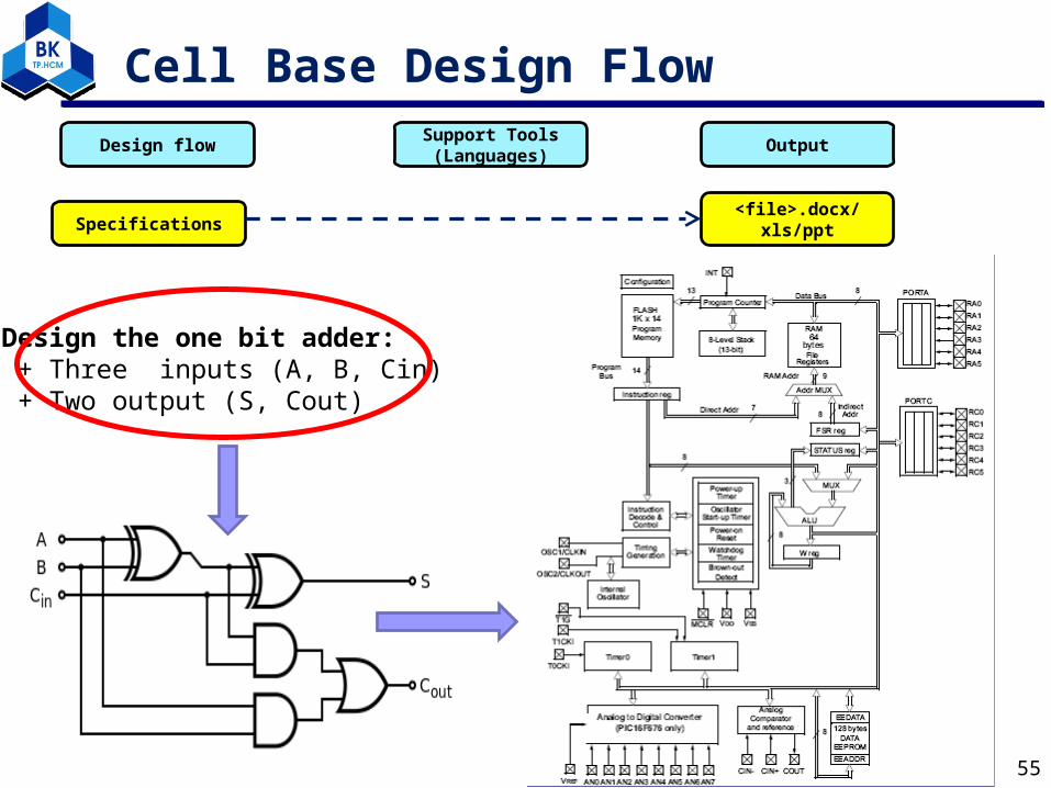
Design the one bit adder: + Three inputs (A, B, Cin) + Two output (S, Cout)
Cell Base Design Flow

12/201212/2012
Specifications
System Level Design
Design flowSupport Tools (Languages)
Output
<file>.docx/xls/ppt
Flatform / ModelsG++ (C++ with
Sysem C class)
C++Methods in
SystemC class
Flatform/Model concepts
TLM class
Cell Base Design Flow
56

12/201212/2012 57
Specifications
System Level Design
RTL Design
Design flow
Design vs. ModelCoding style
Verilog/VHDL language
VI, NotePath++ (Verilog/VHDL) <file>.v
Support Tools (Languages)
Output
<file>.docx/xls/ppt
Cell Base Design Flow

12/201212/2012 58
Specifications
System Level Design
RTL Verification
RTL Design
Design flow
Report file, wave form
VCS/ModelSim, etc(Verilog/ VHDL)
Verification Environment
Check list
VI, NotePath++ (Verilog/VHDL) <file>.v
Support Tools (Languages)
Output
<file>.docx/xls/ppt
VCS tool
Cell Base Design Flow
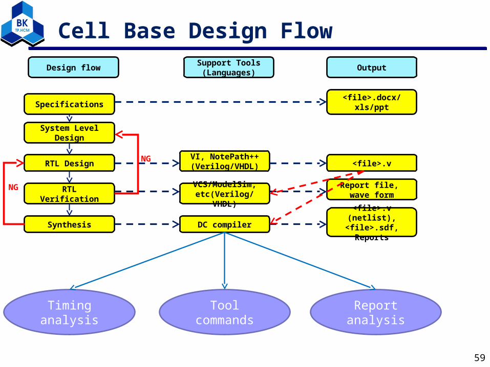
12/201212/2012 59
Specifications
System Level Design
RTL Verification
Synthesis
RTL Design
Design flow
NG VI, NotePath++ (Verilog/VHDL)
DC compiler
<file>.v
Report file, wave form
<file>.v (netlist), <file>.sdf,Reports
VCS/ModelSim, etc(Verilog/ VHDL)
NG
Report analysis
Tool commands
Timing analysis
Support Tools (Languages)
Output
<file>.docx/xls/ppt
Cell Base Design Flow
12/201212/2012 60
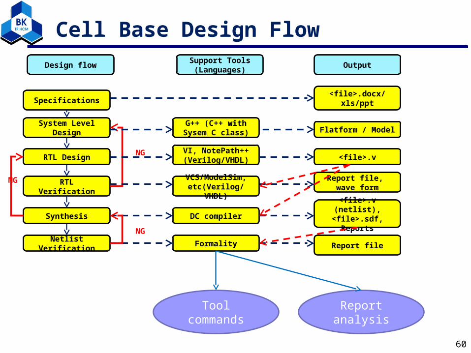
Specifications
System Level Design
RTL Verification
Synthesis
Netlist Verification
RTL DesignNG
Design flowSupport Tools (Languages)
VI, NotePath++ (Verilog/VHDL)
DC compiler
Formality
Output
<file>.docx/xls/ppt
<file>.v
Report file, wave form
<file>.v (netlist), <file>.sdf,Reports
Report file
NG
VCS/ModelSim, etc(Verilog/ VHDL)
Flatform / ModelG++ (C++ with
Sysem C class)
NG
Report analysis
Tool commands
Cell Base Design Flow

12/201212/2012 61
Specifications
System Level Design
RTL Verification
Synthesis
Netlist Verification
DFT
RTL DesignNG
Design flowSupport Tools (Languages)
VI, NotePath++ (Verilog/VHDL)
DC compiler
Formality
Output
<file>.docx/xls/ppt
<file>.v
Report file, wave form
<file>.v (netlist), <file>.sdf,Reports
Report file
NG
VCS/ModelSim, etc(Verilog/ VHDL)
FastScan/Tmax/… Report file, Netlist
Flatform / ModelG++ (C++ with
Sysem C class)
NG
LBISTMBIST
Cell Base Design Flow

12/201212/2012 62
Specifications
System Level Design
RTL Verification
Synthesis
Netlist Verification
DFT
STA
RTL DesignNG
Design flowSupport Tools (Languages)
VI, NotePath++ (Verilog/VHDL)
DC compiler
Formality
Output
<file>.docx/xls/ppt
<file>.v
Report file, wave form
<file>.v (netlist), <file>.sdf,Reports
Report file
NG
Prime Time Report file, Netlist
VCS/ModelSim, etc(Verilog/ VHDL)
FastScan/Tmax/… Report file, Netlist
Flatform / ModelG++ (C++ with
Sysem C class)
NG
Report analysis
Tool commands
Timing analysis
Cell Base Design Flow

12/201212/2012
Cell Base Design Flow
63
DFT
STA
Design flowSupport Tools (Languages)
Output
Prime Time Report file, Netlist
ICC compiler <file>.gdsPlace&Route
FastScan/Tmax/… Report file, Netlist
Tool Commands
Library UsingTiming/Area…
analysis

12/201212/2012 64
ASIC Design Flow
Cell Base & Custom Design Flow Concepts
Custom Design Flow
Cell Base Design Flow
ASIC vs. FPGA Design Flow

12/201212/2012
ASIC vs. FPGA Design Flow
65

12/201212/2012
ASIC vs. FPGA Design Flow
66
ASIC FPGA
1986: Synopsys1987: TSMC1988: Cadence
1983: Altera1984: Xilinx

12/201212/2012
Appendix
67
ASSP : Application Specific Standard Product (DSP, Mircro Processor)ASCP: Application Specific Custom ProductGDS: Graphic Data System

12/201212/2012
Appendix
68
Language Design Level
Simulation
Synthesizeable
Explicit Hardware Resource
Elapsed Time
Sequence
C++ Transaction Yes No No No Yes
SystemC Transaction Yes Yes* No Yes Yes
VHDL RTL Yes Yes* Yes* Yes Yes
Verilog RTL Yes Yes* Yes* Yes Yes
Verilog/VHDL Netlist
Gate Yes Yes Yes Yes Yes
Yes*: Base on the constraints to be able or not

12/201212/2012
Q & AQ & A
69
12/201212/2012
1. “Cell Characterization Concepts” slide - SIVACO company
2. Henrik Eriksson and Per Larsson-Edefors, Tomas Henriksson and Christer Svensson, “Full-Custom vs. Standard-Cell Design Flow - An Adder Case Study”
3. TSMC 65nm CLN65LP HVT Process 1.2-Volt 12-Track AdvantageTM v2.1Standard Cell Library Databook
4. http://www.ami.ac.uk/courses/ami4407_dicdes/u03/
5. http://www.eng.uwo.ca/people/wwang/ece616a/616_extra/notes_web/1_dintro.pdf
6. http://www.ece.ucdavis.edu/~bbaas/116/notes/Handout.std.cell.design.pdf
70
Reference

12/201212/2012
Q1/ Why “Static Timing Analysis” step is only done after “Place and Route” step in FPGA design flow ?
Q2/ In FPGA and ASIC design flows, which ‘s performances such as area and timing are better?
Q3/ Why is “Time to Market” of FPGA design flow faster ?
Q1/ Why “Static Timing Analysis” step is only done after “Place and Route” step in FPGA design flow ?
Q2/ In FPGA and ASIC design flows, which ‘s performances such as area and timing are better?
Q3/ Why is “Time to Market” of FPGA design flow faster ?
71
Question

12/201212/2012 72
Question