1 16 m description gnd drain0
TRANSCRIPT

www.3peakic.com.cn Rev A.0
1 / 12
TPM0596
50-V 8-Ch Low-side Driver Array with Shift Register Interface
Features
8-channel 50-V Low-side Driver Array
500-mA Rated Drain Current (Per Channel)
Very Low Output Leakage < 10 nA Per Channel
Power Efficient with Low RDS-on
Extended Temperature Range: TA = –40°C to 125°C
High-Voltage Outputs 50 V
Compatible with 1.8-V to 5.0-V Logic Interface
Integrated Free-wheeling Diodes for Inductive Load
Improved Noise-immunity with integrated RC filter
ESD Protection Exceeds JESD 22 – 2-kV HBM, 500-V
CDM
Available in 16-pin TSSOP-16 Package
Applications
Inductive Loads
◼ Relays
◼ Unipolar Stepper & Brushed DC Motors
◼ Solenoids & Valves
LED Indicators
Logic Level Shifting
Gate & IGBT Drive
Description
The TPM0596 is a high-voltage, high-current NMOS transistor
array with shift register interface. This device consists of eight
channels of low-side NMOS transistors with high-voltage
outputs and free-wheeling diode for inductive loads.
The maximum drain-current rating of a single NMOS channel is
500 mA. The device supports wide I/O voltage range from 1.8V
to 5V. The transistors can be paralleled for higher current
capability.
The TPM0596 can replace traditional bipolar Darlington arrays
with better thermal efficiency and reliability and saves I/Os.
3 14
2
1
15
16
4 13
M
7
6
5
8
10
11
12
9
SUPPLY
CLR
DRAIN1
DRAIN2
SRCK
DRAIN0GND
TPM0596
RCK DRAIN3
G
SUPPLY
DRAIN5
DRAIN6
DRAIN4
DRAIN7
SER IN
SER OUT
Typical Application Diagram

www.3peakic.com.cn Rev A.0
2 / 12
TPM0596
50-V 8-Ch Low-side Driver Array with Shift Register Interface
Table of Contents
Features ........................................................................................................................................................................... 1
Applications ..................................................................................................................................................................... 1
Description ....................................................................................................................................................................... 1
Table of Contents ............................................................................................................................................................ 2
Order Information ............................................................................................................................................................ 3
Pin Configuration and Functions .................................................................................................................................. 3
Pin Functions ............................................................................................................................................................................... 3
Absolute Maximum Ratings Note 1 ................................................................................................................................... 4
ESD Rating ....................................................................................................................................................................... 4
Recommended Operation Conditions Note 1 .................................................................................................................. 5
Thermal Information ....................................................................................................................................................... 5
Electrical Characteristics ............................................................................................................................................... 6
Typical Performance Characteristics ............................................................................................................................ 7
Detailed Description ....................................................................................................................................................... 9
Package Outline Dimensions ....................................................................................................................................... 11
www.3peakic.com.cn Rev A.0
3 / 12
TPM0596
50-V 8-Ch Low-side Driver Array with Shift Register Interface
Revision History
Date Revision Notes
2020/12/15 Rev A.0 Initial Version
Order Information
Order Number Operating Ambient
Temperature Range Package Marking Information MSL Transport Media, Quantity
TPM0596-TS3R -40 °C – 125 °C (1) TSSOP-16 M0596 MSL3 3000
(1) Ambient temperature indicates device operation condition range. Application thermal behavior needs to be taken care of
when operating in high temperature scenarios.
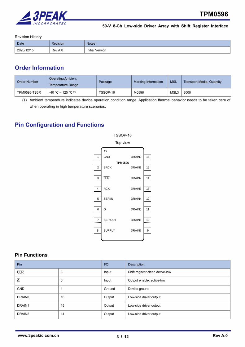
Pin Configuration and Functions
TSSOP-16
Top-view
CLR
DRAIN1
DRAIN2
SRCK
DRAIN0GND
3 14
2
1
15
16
TPM0596
RCK DRAIN34 13
G
7
6
5
SUPPLY8
DRAIN5
DRAIN6
DRAIN4
10
11
12
DRAIN7 9
SER IN
SER OUT
Pin Functions
Pin I/O Description
CLR 3 Input Shift register clear, active-low
G 6 Input Output enable, active-low
GND 1 Ground Device ground
DRAIN0 16 Output Low-side driver output
DRAIN1 15 Output Low-side driver output
DRAIN2 14 Output Low-side driver output

www.3peakic.com.cn Rev A.0
4 / 12
TPM0596
50-V 8-Ch Low-side Driver Array with Shift Register Interface
DRAIN3 13 Output Low-side driver output
DRAIN4 12 Output Low-side driver output
DRAIN5 11 Output Low-side driver output
DRAIN6 10 Output Low-side driver output
DRAIN7 9 Output Low-side driver output
RCK 4 Input Register clock
SER IN 5 Input Serial data input
SER OUT 7 Output Serial data output
SRCK 2 Input Shift register clock
SUPPLY 8 Power Device supply voltage, should be tied above 3.3V.
Absolute Maximum Ratings Note 1
Parameters Rating
Power Supply Voltage, SUPPLY −0.3 V to 55 V
Output Voltage Range DRAIN0 − DRAIN7 −0.3 V to 55 V
Input Voltage Range SER IN, RCK, SRCK, CLR, G −0.3 V to 30 V
Continuous output channel current DRAIN0 − DRAIN7 500 mA
Continuous ground current GND-pin 2 A
Operating Junction Temperature Range –40 °C to 150 °C
Storage Temperature Range –65 °C to 150 °C
Lead Temperature (Soldering, 10 sec) 260 °C
Note 1: Stresses beyond those listed under Absolute Maximum Ratings may cause permanent damage to the device. Exposure to
any Absolute Maximum Rating condition for extended periods may affect device reliability and lifetime.
Note 2: The inputs are protected by ESD protection diodes to each power supply. If the input extends more than 300 mV beyond the
power supply, the input current should be limited to less than 10mA.
Note 3: Power dissipation and thermal limits must be observed.
ESD Rating
Symbol Parameter Condition Minimum Level Unit
HBM Human Body Model ESD ANSI/ESDA/JEDEC JS-001 ±2000 V
CDM Charged Device Model ESD ANSI/ESDA/JEDEC JS-002 ±1500 V

www.3peakic.com.cn Rev A.0
5 / 12
TPM0596
50-V 8-Ch Low-side Driver Array with Shift Register Interface
Recommended Operation Conditions Note 1
Parameters Rating
Power Supply Voltage, SUPPLY 4.5 V to 50 V
Output Voltage Range DRAIN0 − DRAIN7 0 V to 50 V
Logic low voltage 0.9 V
Logic high voltage 1.5 V
Continuous output current DRAIN0 − DRAIN7 500 mA
Operating Ambient Temperature Range –40 °C to 125 °C
Thermal Information
Package Type θJA θJC Unit
TSSOP-16 114.467 50.5482 °C/W

www.3peakic.com.cn Rev A.0
6 / 12
TPM0596
50-V 8-Ch Low-side Driver Array with Shift Register Interface
Electrical Characteristics
All test condition is VCOM = 12 V, TA = −40 °C – 125 °C, unless otherwise noted.
SYMBOL PARAMETER CONDITIONS MIN TYP MAX UNIT
VUVLO COM Under-voltage Lock-Out
Threshold Outputs off; 2.8 3.4 3.6 V
RDS(on) DRAIN0-DRAIN7 output drain-source
on-state resistance
IOUTx = 50 mA, VSUPPLY = 4.5 V
TJ = −40 °C – 125 °C
1.98 4
Ω IOUTx = 100 mA, VSUPPLY = 4.5 V
TJ = −40 °C – 125 °C 2.03 4
IDS-OFF Off-state output leakage current Outputs off; VDRAINx = 12 V 10 500 nA
VOH High-level output voltage, SER OUT IOH = −20 μA 4.4 5.5 6.6 V
IOH = −4 mA 4.2 5.1 6.0 V
VOL Low-level output voltage, SER OUT IOL = 20 μA 0.005 0.01 V
IOL = 4 mA 0.3 0.5 V
VFWD Clamp forward voltage IF = 100 mA 325 mV
IIN(ON) High-Level input current VI = 5 V 1 μA
IIN(OFF) Low-Level input current VI = 0 V -1 μA
ICOM Quiescent supply current Outputs off; VDRAINx = 12 V 15 500 μA
ICOM Active supply current Outputs on; VDRAINx = 0 V 50 500 μA
tpLH Propagation delay time,
LOW to HIGH, from to DRAINx Vpull-up = 12 V; Rpull-up = 48Ω 350 ns
tpHL Propagation delay time,
HIGH to LOW, from to DRAINx Vpull-up = 12 V; Rpull-up = 48Ω 350 ns
TOTP Thermal Shutdown Threshold Outputs off; 150 165 °C

www.3peakic.com.cn Rev A.0
7 / 12
TPM0596
50-V 8-Ch Low-side Driver Array with Shift Register Interface
Typical Performance Characteristics
Figure 1. Output Current Capability vs. Ambient Temperature
Figure 2. Output Current Capability vs. Dutycycle, T = 85 °C
Figure 3. Input Current vs. Input Voltage
Figure 4. Output Voltage vs. Output Current
Ambient Temperature (°C)
Ou
tpu
t C
urr
en
t C
ap
ab
ilit
y (
mA
)
-40 -20 0 20 40 60 80 100 1200
50
100
150
200
250
300
350
400
450
500
550
600
TPM0596-TSSOP161 Channel On2 Channels On3 Channels On4 Channels On5 Channels On6 Channels On7 Channels On8 Channels On
Duty-cycle
Ou
tpu
t C
urr
en
t C
ap
ab
ilit
y (
mA
)
TA = 85°C
0 10% 20% 30% 40% 50% 60% 70% 80% 90% 100%0
50
100
150
200
250
300
350
400
450
500
550
600
TPM0596-TSSOP161 Channel On2 Channels On3 Channels On4 Channels On5 Channels On6 Channels On7 Channels On8 Channels On
Input Voltage (V)
Inp
ut
Cu
rre
nt
(μA
)
0 0.5 1 1.5 2 2.5 3 3.5 4 4.5 5-0.5
0
0.5
1
1.5
2
2.5
3
3.5
4
4.5
5
−40 °C25 °C85 °C125 °C
Output Current (mA)
Ou
tpu
t V
olt
ag
e (
V)
50 100 150 200 250 300 350 400 450 5000
0.5
1
1.5
2
2.5
−40 °C25 °C85 °C125 °C

www.3peakic.com.cn Rev A.0
8 / 12
TPM0596
50-V 8-Ch Low-side Driver Array with Shift Register Interface
Figure 5. Output Diode Forward Voltage Drop vs. Diode Current
Figure 6. Output Leakage Current vs. Temperature
Figure 7. Serial Interface Control
Diode Current (mA)
Dio
de
Fo
rwa
rd V
olt
ag
e (
V)
50 100 150 200 250 300 350 400 450 5000.8
0.85
0.9
0.95
1
1.05
1.1
1.15
1.2
1.25
1.3
1.35
−40 °C25 °C85 °C125 °C
Junction Temperature (°C)
Ou
tpu
t L
ea
ka
ge
Cu
rre
nt
(A
)
-40 -20 0 20 40 60 80 100 120 1400.0002
0.0003
0.00050.0007
0.001
0.002
0.003
0.0050.007
0.01
0.02
0.03
0.050.07
0.1
0.2
0.3
0.5
VOUT = 6 VVOUT = 12 VVOUT = 24 VVOUT = 30 VVOUT = 40 VVOUT = 50 V

www.3peakic.com.cn Rev A.0
9 / 12
TPM0596
50-V 8-Ch Low-side Driver Array with Shift Register Interface
Detailed Description
TPM0596 is an 8-ch low-side driver array. It consists of 8 channels of high-voltage low-side MOSFET. Its outputs can drive inductive
loads up to 500mA per channel with wide temperature range. Its outputs can drive inductive loads, such as solenoids, relays, motors
and lamps up to 500mA per channel with wide temperature range. Multiple channels can be paralleled to increase driving capabilities
or reduce thermal dissipation.
TPM0596 has various benefits to increase system robustness and ease of use. It can replace discrete bipolar components and
various version of bipolar-based Darlington arrays.
The device uses serial shift register to control outputs. Shift register interface helps system to save I/Os by using minimal 3 pins only.
The input pins support a wide range of voltage ratings from 1.8V logic, TTL logic up to 30V voltage rail. With integrated noise-filter,
the inputs improve system robustness in support robust industrial environment. The CMOS input gates can support modern
microcontrollers without the needs of current sourcing capabilities on microcontroller GPIOs.
The minimal I/Os are SRCK, RCK, SER IN. SER OUT is optional to read back the shift register values to improve system robustness.
SER OUT needs external pull-up resistor, 3PEAK recommends a 10kΩ pull-up resistor. G is output gating control input, setting G
to low disables all outputs. CLR is the chip level clear input. Setting CLR to low can clear the internal shift registers.
Integrated over temperature protection and under-voltage lock out protection provides advanced robustness to the system comparing
to older generation of Darlington arrays. The low on-resistance of output ensures lower power dissipated on the device. The low on-
resistance increases driving efficiency and reduces device temperature, thus improves the system robustness.
The device also supports a wide ambient temperature range (−40°C to 125°C)
SRCK
G
SER IN
RCK
CLR
OUT1
7 6 5 4 3 2 1 0
Figure 8 Shift Register Diagram

www.3peakic.com.cn Rev A.0
10 / 12
TPM0596
50-V 8-Ch Low-side Driver Array with Shift Register Interface
Block
GND
C1
CLR
D
C1
CLR
D
C1
CLR
D
C1
CLR
D
C1
CLR
D
C1
CLR
D
C1
CLR
D
C1
CLR
D
C1
CLR
D
C2
CLR
D
C2
CLR
D
C2
CLR
D
C2
CLR
D
C2
CLR
D
C2
CLR
D
C2
CLR
D
C2
CLR
D
SER IN
SRCK
RCK
G
CLR16
DRAIN0
15DRAIN1
DRAIN2
DRAIN3
DRAIN4
DRAIN5
DRAIN6
DRAIN7
SER OUT
SUPPLY8
14
13
12
11
10
9
1
7
6
4
3
2
5
TPM0596
Figure 9 Functional Block Diagram
Device Thermal Capability
DRAIN0 to DRAIN7 drives loads with 100-Ω resistance and 1.36-mH inductance with 10kHz frequency and 50% dutycycle. The
package top temperature is measured as 58.9 °C.

www.3peakic.com.cn Rev A.0
11 / 12
TPM0596
50-V 8-Ch Low-side Driver Array with Shift Register Interface
Package Outline Dimensions
TSSOP-16

www.3peakic.com.cn Rev A.0
12 / 12
TPM0596
50-V 8-Ch Low-side Driver Array with Shift Register Interface
Order Number Package D1
(mm)
W1
(mm)
A0(mm) B0(mm) K0(mm) P0(mm) W0(mm) Pin1
Quadrant
TPM0596-TS3R TSSOP-16 330.0 17.6 6.8 5.4 1.3 8.0 12.0 Q1
3PEAK and the 3PEAK logo are registered trademarks of 3PEAK INCORPORATED. All
other trademarks are the property of their respective owners.