1 5.5 a multicycle implementation a single memory unit is used for both instructions and data. there...
Post on 20-Dec-2015
215 views
TRANSCRIPT

1
5.5 A Multicycle Implementation
• A single memory unit is used for both instructions and data.• There is a single ALU, rather than an ALU and two adders.• One or more registers are added after every major functional unit.

2
Continue
Replacing the three ALUs of the single-cycle by a single ALU means that the single ALU must accommodate all the inputs that used to go to the three different ALUs.

3
Continue
Control signals:• The programmer-visible state units (PC, Memory, Register file) and IR write
Memory Read• ALU control: same as single cycle• Multiplexor single/two control lines

4
Continue
Three possible sources for the PC:1. PC+42. ALUOut : address of the beq3. Address for jump ( j )
PC write control signal: PCWrite : PC+4 and jump PCWriteCond : beq

5
Continue
6
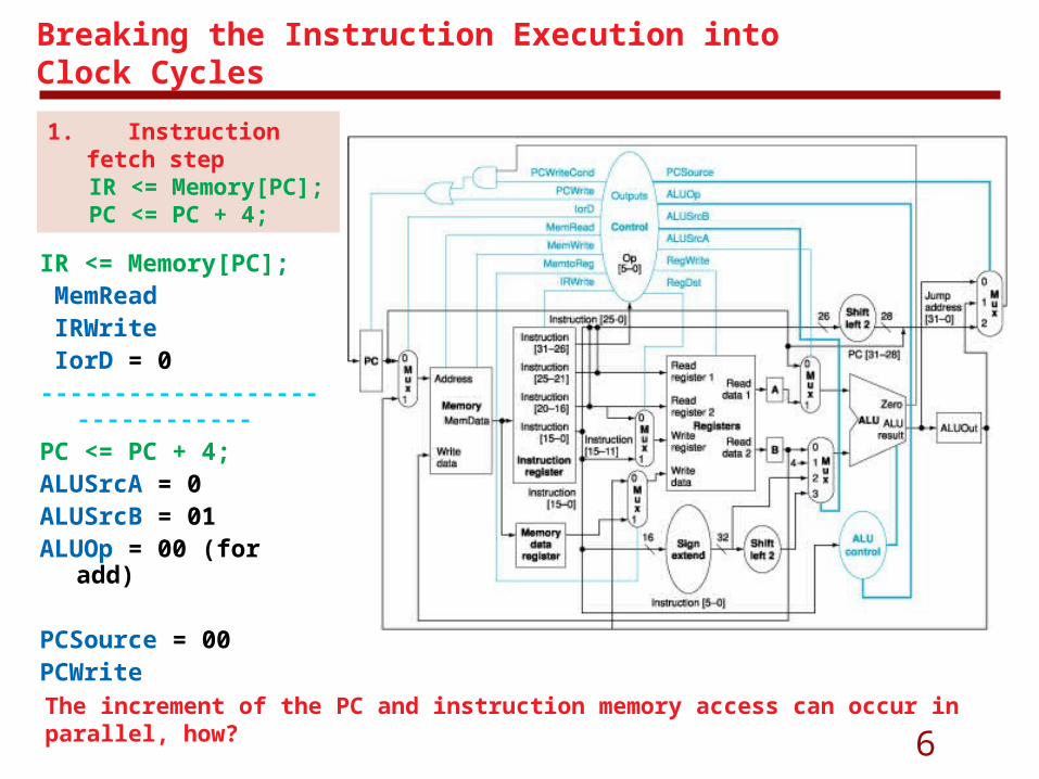
Breaking the Instruction Execution into Clock Cycles
IR <= Memory[PC]; MemRead IRWrite IorD = 0-------------------------------PC <= PC + 4;ALUSrcA = 0ALUSrcB = 01ALUOp = 00 (for add)
PCSource = 00PCWrite
The increment of the PC and instruction memory access can occur in parallel, how?
1. Instruction fetch step
IR <= Memory[PC]; PC <= PC + 4;
7
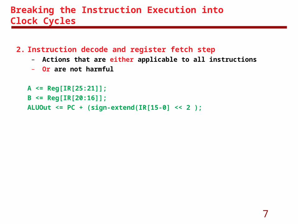
Breaking the Instruction Execution into Clock Cycles
2. Instruction decode and register fetch step– Actions that are either applicable to all instructions– Or are not harmful
A <= Reg[IR[25:21]];
B <= Reg[IR[20:16]];
ALUOut <= PC + (sign-extend(IR[15-0] << 2 );
8
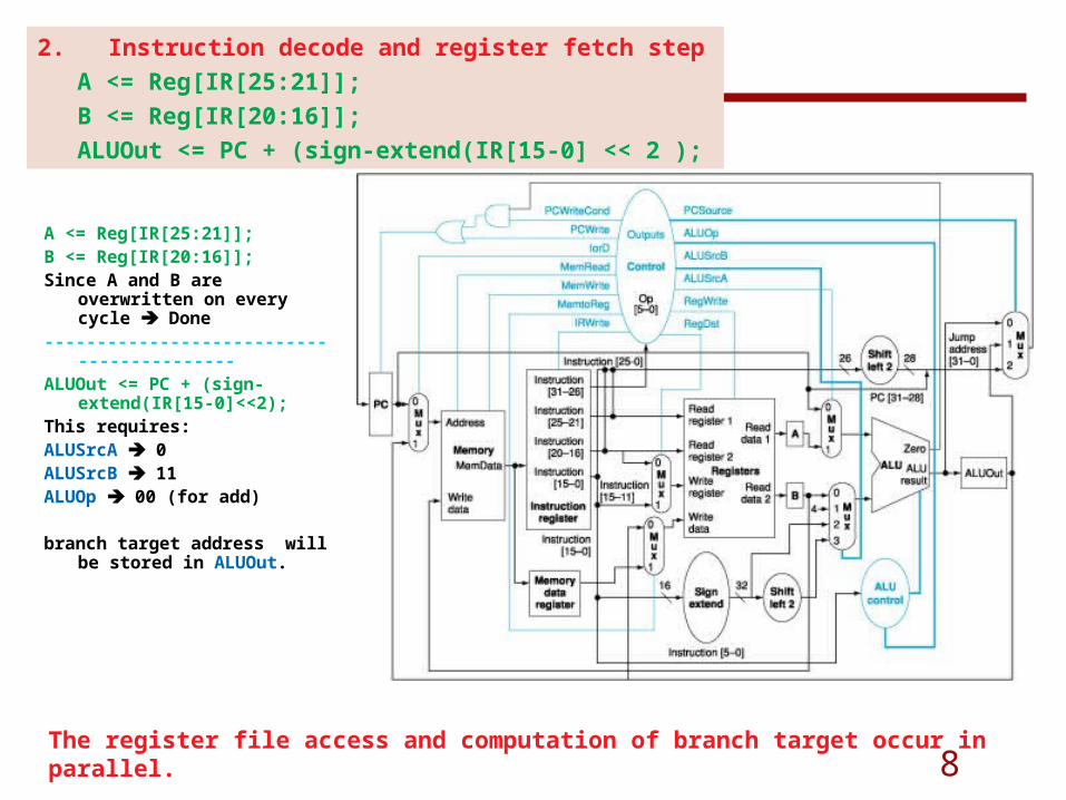
A <= Reg[IR[25:21]];B <= Reg[IR[20:16]];Since A and B are overwritten
on every cycle Done------------------------------------------ALUOut <= PC + (sign-
extend(IR[15-0]<<2);This requires:ALUSrcA 0ALUSrcB 11ALUOp 00 (for add)
branch target address will be stored in ALUOut.
The register file access and computation of branch target occur in parallel.
2. Instruction decode and register fetch step
A <= Reg[IR[25:21]];
B <= Reg[IR[20:16]];
ALUOut <= PC + (sign-extend(IR[15-0] << 2 );

9
Breaking the Instruction Execution into Clock Cycles
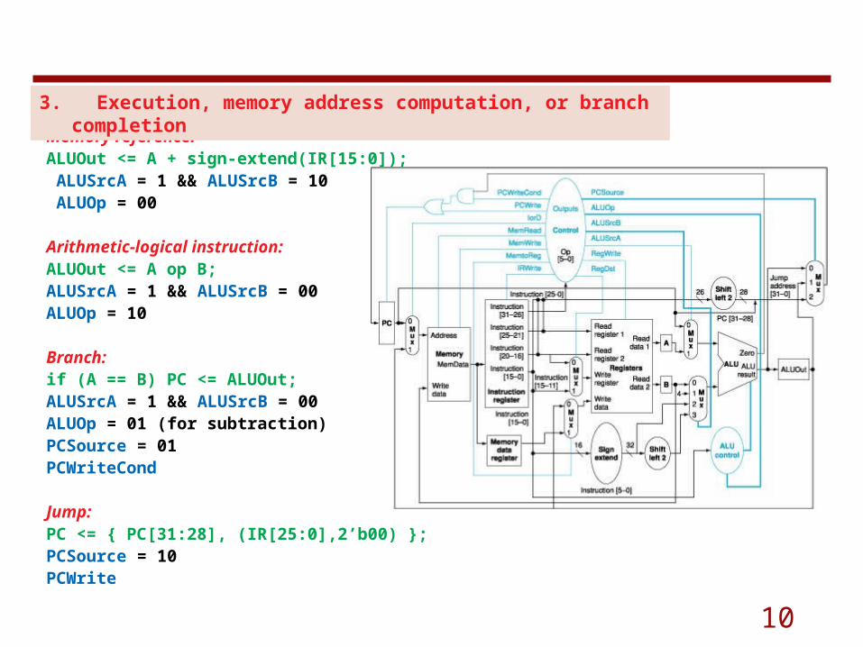
3. Execution, memory address computation, or branch completion
Memory reference:
ALUOut <= A + sign-extend(IR[15:0]);
Arithmetic-logical instruction:
ALUOut <= A op B;
Branch:
if (A == B) PC <= ALUOut;
Jump:
PC <= { PC[31:28], (IR[25:0], 2’b00) };
10
Memory reference:ALUOut <= A + sign-extend(IR[15:0]); ALUSrcA = 1 && ALUSrcB = 10 ALUOp = 00
Arithmetic-logical instruction:ALUOut <= A op B;ALUSrcA = 1 && ALUSrcB = 00 ALUOp = 10
Branch:if (A == B) PC <= ALUOut;ALUSrcA = 1 && ALUSrcB = 00 ALUOp = 01 (for subtraction)PCSource = 01PCWriteCond
Jump:PC <= { PC[31:28], (IR[25:0],2’b00) };PCSource = 10PCWrite
3. Execution, memory address computation, or branch completion

11
Breaking the Instruction Execution into Clock Cycles
4. Memory access or R-type instruction completion step
Memory reference:MDR <= Memory [ALUOut]; MemRead
or IorD=1Memory [ALUOut] <= B; MemWrite
Arithmetic-logical instruction (R-type):
Reg[IR[15:11]] <= ALUOut; RegDst=1 RegWriteMemtoReg=0
5. Memory read completion step
Load:Reg[IR[20:16]] <= MDR; MemtoReg=1 RegWrite
RegDst=0

12
Breaking the Instruction Execution into Clock Cycles
13
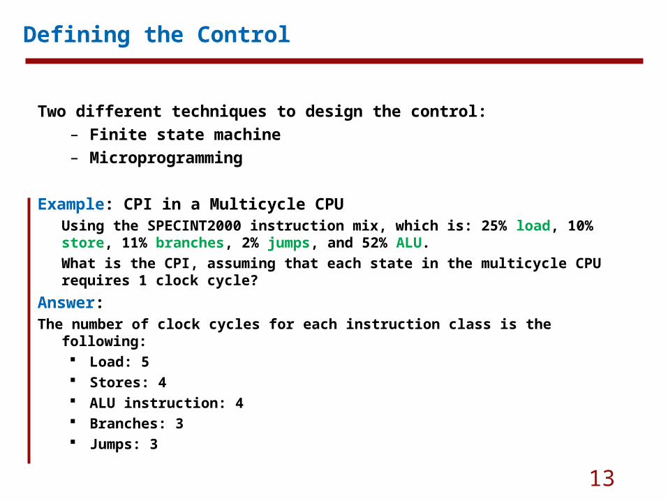
Defining the Control
Two different techniques to design the control:
– Finite state machine
– Microprogramming
Example: CPI in a Multicycle CPUUsing the SPECINT2000 instruction mix, which is: 25% load, 10% store, 11% branches, 2% jumps, and 52% ALU.
What is the CPI, assuming that each state in the multicycle CPU requires 1 clock cycle?
Answer:The number of clock cycles for each instruction class is the following:
Load: 5 Stores: 4 ALU instruction: 4 Branches: 3 Jumps: 3
14
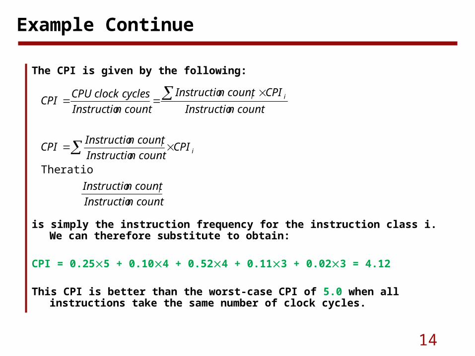
Example Continue
The CPI is given by the following:
is simply the instruction frequency for the instruction class i. We can therefore substitute to obtain:
CPI = 0.255 + 0.104 + 0.524 + 0.113 + 0.023 = 4.12
This CPI is better than the worst-case CPI of 5.0 when all instructions take the same number of clock cycles.
n countInstructio
n countInstructio
CPIn countInstructio
n countInstructioCPI
n count Instructio
CPI n countInstructio
n countInstructio
cyclesCPU clock CPI
i
ii
ii
ratio The

15
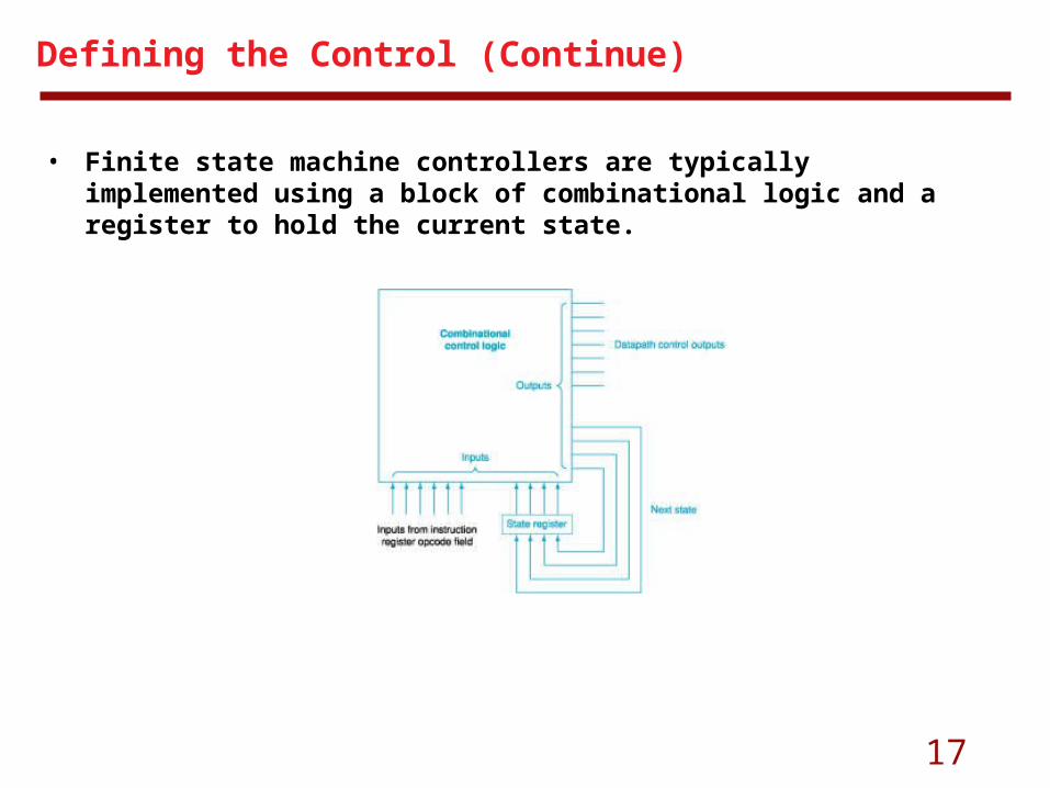
Defining the Control (Continue)

16
Defining the Control (Continue)
The complete finite state machine control
17
Defining the Control (Continue)
• Finite state machine controllers are typically implemented using a block of combinational logic and a register to hold the current state.
18
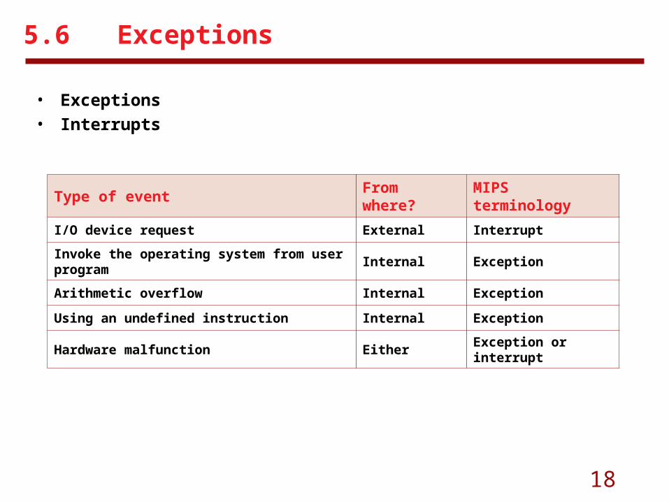
5.6 Exceptions
• Exceptions
• Interrupts
Type of event From where? MIPS terminology
I/O device request External Interrupt
Invoke the operating system from user program
Internal Exception
Arithmetic overflow Internal Exception
Using an undefined instruction Internal Exception
Hardware malfunction Either Exception or interrupt

19
How Exception Are Handled
To communicate the reason for an exception:
1. a status register ( called the Cause register)
2. vectored interrupts
Exception type Exception vector address (in hex)
Undefined instruction C000 0000hex
Arithmetic overflow C000 0020hex

20
How Control Checks for Exception
Assume two possible exceptions: Undefined instruction Arithmetic overflow

21
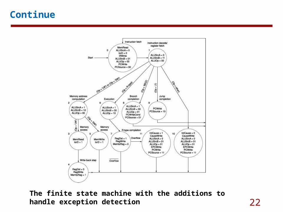
Continue
The multicycle datapath with the addition needed to implement exceptions
22
Continue
The finite state machine with the additions to handle exception detection