1. capsense sigma-delta user module capsense™ sigma-delta...
TRANSCRIPT
Cypress Semiconductor Corporation • 198 Champion Court • San Jose, CA 95134-1709 • 408-943-2600Document Number: 001-13536 Rev. *C Revised February 12, 2009
1. CapSense Sigma-Delta User Module
Copyright © 2007-2009 Cypress Semiconductor Corporation. All Rights Reserved.
For one or more fully configured, functional example projects that use this User Module go to www.cypress.com/psocexampleprojects.
Features and Overview• Scan 1 to 46 capacitive sensors.• Sensing possible with up to a 15-mm glass overlay.• Proximity detection to 20 cm with a wire-based sensor.• High immunity to AC mains noise, EMC noise, and power supply voltage changes.• Supports different combinations of independent and slide capacitive sensors.• Double slide sensor physical resolution using diplexing.• Increase slide sensor resolution using interpolation.• Touchpad support with two slide sensors.• Sensing support via high-resistive conductive materials (ITO films for example).• Shield electrode support for reliable operation in the presence of water film or droplets.• Guided sensor and pin assignments using the CSD Wizard.
CapSense™ Sigma-Delta Data Sheet CSD
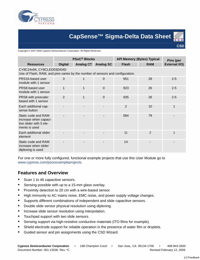
ResourcesPSoC® Blocks API Memory (Bytes) Typical Pins (per
External I/O)Digital Analog CT Analog SC Flash RAMCY8C24x94, CY8CLED03D/04DUse of Flash, RAM, and pins varies by the number of sensors and configuration. PRS16-based user module with 1 sensor
3 1 0 951 28 2-5
PRS8-based user module with 1 sensor
1 1 0 923 26 2-5
PRS8 with prescaler based with 1 sensor
2 1 0 935 26 2-5
Each additional cap-sense button
- - - 2 10 1
Static code and RAM increase when capaci-tive slider with 5 ele-ments is used
- - - 584 79 -
Each additional slider element
- - - 11 2 1
Static code and RAM increase when slider diplexing is used
- - - 14 - -
[+] Feedback
CapSense Sigma-Delta User Module
Document Number: 001-13536 Rev. *C Page 2 of 67
• Integrated baseline update algorithm for handling temperature, humidity, and electrostatic discharge (ESD) events.
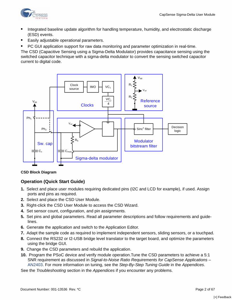
• Easily adjustable operational parameters. • PC GUI application support for raw data monitoring and parameter optimization in real-time.The CSD (Capacitive Sensing using a Sigma-Delta Modulator) provides capacitance sensing using the switched capacitor technique with a sigma-delta modulator to convert the sensing switched capacitor current to digital code.
CSD Block Diagram
Operation (Quick Start Guide)1. Select and place user modules requiring dedicated pins (I2C and LCD for example), if used. Assign
ports and pins as required. 2. Select and place the CSD User Module. 3. Right-click the CSD User Module to access the CSD Wizard. 4. Set sensor count, configuration, and pin assignments. 5. Set pins and global parameters. Read all parameter descriptions and follow requirements and guide-
lines.6. Generate the application and switch to the Application Editor. 7. Adapt the sample code as required to implement independent sensors, sliding sensors, or a touchpad. 8. Connect the RS232 or I2-USB bridge level translator to the target board, and optimize the parameters
using the bridge GUI.9. Change the CSD parameters and rebuild the application. 10. Program the PSoC device and verify module operation.Tune the CSD parameters to achieve a 5:1
SNR requirement as discussed in Signal-to-Noise Ratio Requirements for CapSense Applications – AN2403. For more information on tuning, see the Step-By-Step Tuning Guide in the Appendices.
See the Troubleshooting section in the Appendices if you encounter any problems.
Clock source
Rb
Cmod
Vref
Cx
Vdd
Ph1
Ph2
VC1
Decision logic
IMO
Sigma-delta modulator
Modulator bitstream filter
Clocks
Sw. cap
Reference source
1VC4
Sincn filter
Vref
Vdd
R2
R1
[+] Feedback
CapSense Sigma-Delta User Module
Document Number: 001-13536 Rev. *C Page 3 of 67
Functional DescriptionA capacitive sensor array consists of combinations of independent sensors, sliding sensors, and touchpads implemented as a pair of orthogonal sliders. High level decision logic provides compensation for environmental factors, such as temperature, humidity, and power supply voltage change. A separate shield electrode can be used for shielding the sensor array to reduce stray capacitance, providing more reliable operation in the presence of a water film or droplets.The high-level software functions accommodate slider diplexing so that a single electrical sensor may be used in two physical locations for resolution enhancement. The functions also provide further interpolation of resolved sensor position between physical sensor locations.The capacitive sensor consists of physical, electrical, and software components:Physical
The physical sensor itself, typically a conductive pattern constructed on a PCB connected to the PSoC with an insulating cover, a flexible membrane, or a transparent overlay over a display.
Electrical A method to convert the sensor capacitance to digital format. The conversion system consists of a sensing switched capacitor, a sigma-delta modulator, and a counter-based digital filter to convert the modulator output bit stream to a readable digital format.
Software
• Detection and compensation software algorithms convert the count value into a sensor detection deci-sion.
• In the case of consecutive, dependent sensors (sliders and touchpads, for example) APIs are provided to interpolate a position with greater resolution than the physical pitch of the sensors. For example, you can create a volume slider with 10 sensors and use the provided firmware to expand the number of volume levels to 100. Alternatively, using the same APIs, you can use two capacitive sensors that taper into each other and determine the position of a conductive object (such as a finger) between them.
While there are a number of methods to measure capacitance, the one used in this user module is combination switching capacitor with delta-sigma modulator.The following documents are recommended reading before you use the CSD User Module for the first time.
• CY8C21x34 Series PSoC Mixed Signal Array Technical Reference Manual, sections• Two Column Limited Analog• Digital Clocks• IO Analog Multiplexer
• Understanding Switched Capacitor Analog Blocks – AN2041
The following application notes are recommended after reading the CSD User Module documentation. Application notes can be found on the Cypress Semiconductor web site at www.cypress.com:
• CapSense Best Practices – AN2394• Signal-to-Noise Ratio Requirements for CapSense Applications – AN2403• Charting Tool to Debug CapSense Applications – AN2397• EMC Design Considerations for PSoC CapSense Applications – AN2318• Power Consumption and Sleep Considerations in Capacitive Sensing Applications – AN2360
[+] Feedback
CapSense Sigma-Delta User Module
Document Number: 001-13536 Rev. *C Page 4 of 67
• Layout Guidelines for PSoC CapSense – AN2292• Software Implementation of a Universal Asynchronous Transmitter – AN2399• Waterproof Capacitance Sensing – AN2398
Capacitance Physics FundamentalsSuppose there is a solitary conductive object that has a non-compensated charge, Q. This charge creates a static electric field outside the object. The potential ϕ is linearly proportional to the charge Q:
Equation 1
Capacitance is the coefficient that links the object’s potential ϕ with its charge Q. This coefficient depends only on the conductor’s geometric dimensions. If the conductive object is covered with a dielectric, the object’s capacitance depends on the dielectric characteristics and geometry. For example, for a solitary sphere with radius R covered with an isotropic material with a dielectric constant ε, the sphere’s capacitance can be easy calculated with the following equation:
Equation 2
– permittivity constant (8.85x10⁻¹²F/m)
– relative permittivity of the dielectric material that covers the sphere
For objects with arbitrary dimensions the capacitance calculation is difficult or impossible. In many cases, the capacitance is calculated using Equation 2 and some equivalent radius, Re. For example, for a rectangular box with orthogonal edge dimensions a, b, c, the equivalent radius Re can be defined as the arithmetic mean of its dimensions:
Equation 3
This allows you to calculate the capacitance of an item based on its dimensions with suitable accuracy for practical evaluations. By substituting the a = 1.8m, b = 0.4m, c = 0.3m we can estimate the capacitance of the human body at 92 pF. This is very close to the 100 pF value used in the Human Body Model (HBM) for the electrostatic discharge (ESD) sensitivity testing. Any conductive object (even if it is not connected to any other objects) has its own capacitance that is determined by the object’s geometry and dimensions. Humans, coils, metallic pens, and so on, all have their own capacitance. It is not necessary to connect a second capacitor terminal to anything (system ground, for example). But to use circuit theory for CapSense™ systems analysis, a second capacitor terminal can be connected to any net with a fixed potential (ground or power supply nets, for example).When other conductive, noncharged objects are located close to the conductive charged object, the electric field induces the charges on these objects to reduce the electric field intensity and increase the conductive object’s capacitance. Two conductive items charged to equal but opposite charges form a capacitor. The most commonly used is a parallel plate capacitor. Its capacitance can be calculated using the following equation:
Equation 4
ϕ QC----=
C 4πεε0R=
ε0
ε
Rea b c+ +
3---------------------=
Cεε0S
d-----------=
[+] Feedback
CapSense Sigma-Delta User Module
Document Number: 001-13536 Rev. *C Page 5 of 67
S – plate area in square unitsd – distance between platesEquation 4 is accurate only when the distance between plates is much less than the plate mechanical dimensions, therefore, electric field is considered located only between the plates. Capacitance can be easily calculated analytically only for simple electrode systems, such as plate, sphere, or cylinder capacitors. For arbitrary electrodes, system capacitance can be found by solving Poisson partial differential equation using numerical methods. Modern CAD field analysis tools (FELAB, ANSYS, and others) greatly simplify this work. The capacitance estimation is required in many real CapSense applications, where a complex electrodes/dielectrics combination is used and analytical equations do not provide sufficient for accuracy in practical use.In most CapSense applications, the sensing plate is covered by an insulation overlay. The overlay thickness and the dielectric constant value of the material determines the inter-capacitance between the sensing electrode and the human finger. For example, for a white goods application where the overlay is hardened glass with a dielectric constant of 7, the sensing zone diameter is 10 mm and the overlay thickness is 6 mm, we can estimate the sensor electrode-finger capacitance approximately (here the overlay thickness is on the same order as sensing zone diameter, so boundary effects have a noticeable influence) using Equation 4 to 1.0 pF. Taking into account that human capacitance is more than 100 pF, the sensing electrode-finger capacitance is a dominant factor in the capacitance sensing application’s operation.Real application capacitance includes additional components that should be taken into account. Suppose we have an isolated PCB with a button sensing electrode. An example of this application can be a cell phone, a remote control, or other small device. The following main capacitance components are shown in the figure below:
• Finger-electrode capacitance, Cfe. Values are 0.1−10 pF, depending on electrode size and overlay thickness, and the dielectric constant of the electrode.
• Human capacitance, Ch. Approximately 100−300 pF.• Board capacitance, Cb. Value is 10−20 pF for small boards without external connections (for example,
a remote control) to more than 1000 pF when the device is connected to AC mains (for example, a mobile phone when attached to a charger or an externally powered stereo system).
• Board-human capacitance, Chb. Values are 1−20 pF depending on target board dimensions, insulation thickness, and hand locations.
[+] Feedback
CapSense Sigma-Delta User Module
Document Number: 001-13536 Rev. *C Page 6 of 67
A Touch Application Capacitance Model
From the point of view of the PSoC device sensing touch capacitance, Cx is a series of connections of the finger-electrode capacitance Cfe with equivalent ground capacitance:
Equation 5
As can be seen from Equation 5, the equivalent touch capacitance Cx is less than the finger-electrode capacitance Cfe. This touch capacitance reduction is negligible in most CapSense applications, but needs to be taken into account for small, autonomous systems that can sometimes use external connections.The CapSense system should be able to detect small capacitance changes (Cx = 0.1 − 10 pF) and the presence of large parasitic capacitance (10 − 300 pF). The parasitic capacitance components are the electrode’s capacitance, capacitance between the sensing electrode and the ground plane, and the inter-capacitance between neighboring traces on the PCB. The total capacitance that is measured by the CapSense system is the sum of parasitic Cpar and touch capacitances Cx:
Equation 6
Capacitance Measurement OperationThe capacitance to code converter consists of five main parts:
• Sensing switched capacitor• Sigma-delta modulator
Sensor PSoC
Cb
Cfe
Ch
Cx
Chb
Cx =Cb Ch
ChbCfe
Cx<Cfe
Cx ChbCh Cb⋅Ch Cb+-------------------+⎝ ⎠
⎛ ⎞ 1– 1Cfe-------+⎝ ⎠
⎛ ⎞ 1–=
Cs Cx Cpar+=
[+] Feedback
CapSense Sigma-Delta User Module
Document Number: 001-13536 Rev. *C Page 7 of 67
• Modulator bit stream filter• Clock source• Comparator reference sourceThe decision logic is implemented in firmware. The firmware analyzes capacitance measurement, tracks the slow capacitance change due to environmental factors, and runs decision logic to detect button touches and calculate slider position.
CSD Block Diagram
Sensing Switched CapacitorThe switches Sw1and Sw2 operate in two nonoverlapping phases, Ph1 and Ph2. Break-before-make precharge switches are used for this. At phase Ph1 (when clock signal is high) Sw1 is on. At phase Ph2 (when clock signal is low) Sw2 is on. Sw1 and Sw2 are never on at the same time.
The Switched Capacitor is Equivalent to the Resistor Between the Power Supply and Modulator Input
Latch
Rb
Cmod
Vref
Cx
Vdd
Ph1
Ph2 Decision logic
Sigma-delta modulator
Clocks
Sw. cap
Sw1
Sw2
Sw3
VCmodCMP
Firmware
PRS VC1IMO
1VC4
Modulator bitstream filter
Sincn filter
Reference source
Vref
Vdd
R2
R1
Cs
Vdd
Ph1
Ph2
Sw1
Sw2 VCmod
Re=
Vdd
VCmod
[+] Feedback
CapSense Sigma-Delta User Module
Document Number: 001-13536 Rev. *C Page 8 of 67
The sensing capacitor is charged to the supply voltage Vdd at phase Ph1 and is discharged to the modulator capacitor Cmod at phase Ph2. The sensing switched capacitor is equivalent to the resistor Rc with equivalent resistance value to:
Equation 7
fs – Sw1, Sw2 operation frequency.
Refer to AN2041, Understanding Switched Capacitor Analog Blocks, for proof of the equation and valuable information about switched capacitor circuit operation. The current from the switched capacitor resistor flows to the sigma-delta modulator, charging the capacitor Cmod.
Sigma-Delta ModulatorThe modulator is formed by a comparator, a comparator latch, an modulation capacitor Cmod, and a discharge resistor Rb. When the modulation capacitor voltage VCmod reaches the comparator reference voltage Vref, the comparator toggles and turns on the capacitor discharge resistor Rb via switch Sw3. The capacitor voltage starts dropping. When the modulator capacitor voltage falls below the reference voltage, the discharging resistor is disconnected. The modulator capacitor voltage starts rising again, repeating the modulation capacitor charge/discharge cycles. The latch makes comparator operation synchronized to the clock VC1/4 (internal column rate) signal and limits minimum discharge switch Sw3 on/off time. The modulator keeps the modulator capacitor voltage VCmod close to the reference voltage Vref in average by alternatively turning on/off the discharge switch Sw3.
The Sigma-Delta Modulator with Equivalent Switched Capacitor Resistor Rc
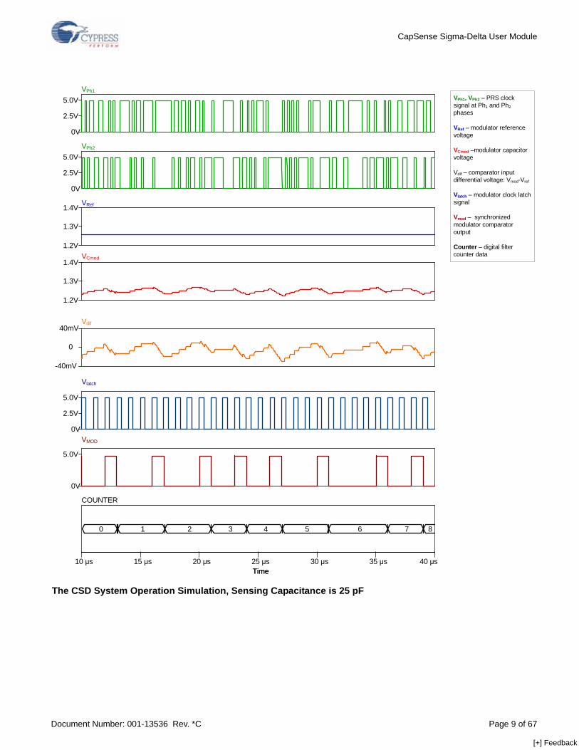
The figures below demonstrate the system operation SPICE (Simulation Program with Integrated Circuits Emphasis) simulation at different sensing capacitor values.
Rc1
fsCs----------=
Latch
Rb
Cmod
Vref
Sw3
VCmodCMP
Rc
IMO
vdd
Vmod (output bitstream)
1VC4
[+] Feedback
CapSense Sigma-Delta User Module
Document Number: 001-13536 Rev. *C Page 9 of 67
The CSD System Operation Simulation, Sensing Capacitance is 25 pF
TimeTime10 µs 15 µs 20 µs 25 µs 30 µs 35 µs 40 µs
COUNTER
0V
5.0V
0V
2.5V
5.0V
Vlatch
Vdif
1.2V
1.3V
1.4V
0V
2.5V
5.0V
0V
2.5V
5.0V
VMOD
-40mV
0
40mV
1.2V
1.3V
1.4VVCmod
VRef
VPh2
VPh1VPh1, VPh2 – PRS clock signal at Ph1 and Ph2phases
VRef – modulator reference voltage
VCmod –modulator capacitor voltage
Vdif – comparator input differential voltage: Vmod-Vref
Vlatch – modulator clock latch signal
Vmod – synchronized modulator comparator output
Counter – digital filter counter data
0 1 2 3 4 5 6 7 8
[+] Feedback
CapSense Sigma-Delta User Module
Document Number: 001-13536 Rev. *C Page 10 of 67
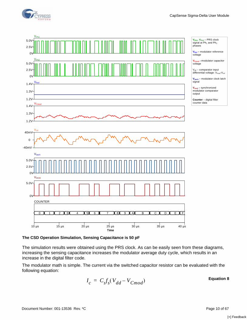
The CSD Operation Simulation, Sensing Capacitance is 50 pF
The simulation results were obtained using the PRS clock. As can be easily seen from these diagrams, increasing the sensing capacitance increases the modulator average duty cycle, which results in an increase in the digital filter code.The modulator math is simple. The current via the switched capacitor resistor can be evaluated with the following equation:
Equation 8
Time Time10 µs 15 µs 20 µs 25 µs 30 µs 35 µs 40 µs
COUNTER
0V
5.0V
0V
2.5V
5.0V
Vlatch
Vdif
1.2V
1.3V
1.4V
0V
2.5V
5.0V
0V
2.5V
5.0V
VMOD
-40mV
0
40mV
1.2V
1.3V
1.4VVCmod
VRef
VPh2
VPh1VPh1, VPh2 – PRS clock signal at Ph1 and Ph2 phases
VRef – modulator reference voltage
VCmod –modulator capacitor voltage
Vdif – comparator input differential voltage: Vmod-Vref
Vlatch – modulator clock latch signal
Vmod – synchronized modulator comparator output
Counter – digital filter counter data
0 1 2 3 4 5 6 7 8 9 A B C D E F
Ic Csfs Vdd VCmod–( )=
[+] Feedback
CapSense Sigma-Delta User Module
Document Number: 001-13536 Rev. *C Page 11 of 67
Because the switched capacitor resistor current is directly proportional to the supply voltage value, the reference voltage should be set proportional to this voltage to minimize the code dependence from a power supply voltage change.
Equation 9
kd – The proportionality coefficient is determined by the resistors values R1 and R2. The relationship is as follows:
Equation 10
The modulator output bit stream duty cycle dmod carries information about the sensing capacitor value. The averaged current via the bias resistor can be expressed as follows:
Equation 11
The sigma-delta modulator keeps these currents close to equal in average by keeping the modulator capacitor voltage equal to the reference voltage in average. By substituting and taking into account Equation 8, we can obtain:
Equation 12
Equation 12 determines the maximum sensing capacitance value, which can be measured for given parameters set: , or:
Equation 13
The resolution for the method can be evaluated by differentiating Equation 12 and resolving relatively :
Equation 14
If you evaluate the Cxmax and ΔCx values by substituting the following values: kd = 0.25, Rb = 1.6 kΩ, fs = 6MHz, and the duty cycle is measured with 12 bit resolution, you get: Cxmax = 17 pF, the resolution is ΔCx = 0.01 pF. As seen in Equation 12 and Equation 14, the duty cycle is linearly proportional to the sensing capacitance and the resolution is constant regardless of sensing capacitance, making linear position sensing devices easy.
Vref kdVdd=
kdR2
R1 R2+-------------------=
IRbdmodVCmod
Rb------------------------------=
Ic IRb=
dmod CsfsRb1kd----- 1–⎝ ⎠
⎛ ⎞=
dmod 1≤
Csmaxkd
1 kd–-------------- 1
Rbf--------
s=
ΔCx
ΔCxkd
1 kd–-------------- 1
Rbfs----------Δdmod=
[+] Feedback

CapSense Sigma-Delta User Module
Document Number: 001-13536 Rev. *C Page 12 of 67
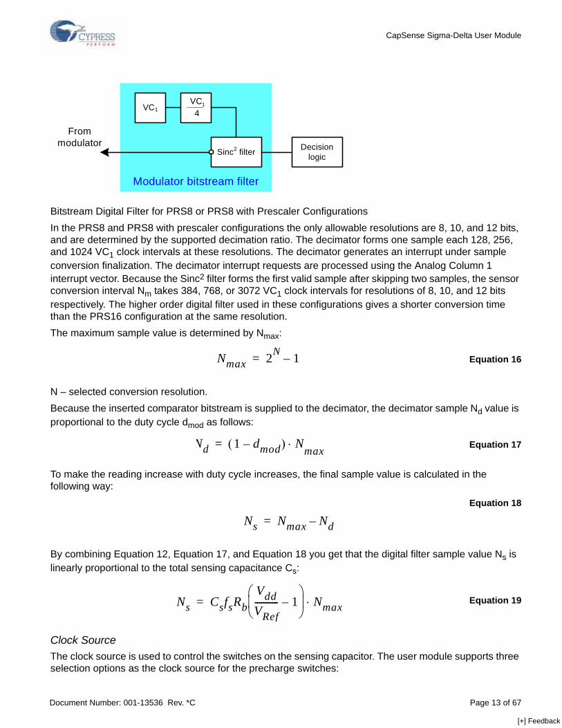
Modulator Bit Stream FilterThe modulator converts the capacitance to the output bit stream duty cycle. The duty cycle is measured using a Sincn digital filter, based on the hardware decimator, available in the 24x94 devices. The decimator is configured in the different operation modes and configurations for optimal performance. When the PRS16 configuration is selected, the decimator is configured in the single integration mode (sinc, or incremental filter). The decimation rate is set by the external timer.
Bitstream Digital Filter for PRS16 Configuration
One sample is formed each Nm IMO cycles. The conversion interval is set with the external decimator capture timer period Ts and software overflow counter that is used for hardware timer interval extension. If the software overflow counter is equal to Ns, the sample conversion interval can be evaluated in the IMO cycles using:
Equation 15
VC1, VC2 – divider values
Ts – capture timer period
Ns – software counter value
The VC1 value is changed in the user module API to get different sensor scanning speeds. The VC2 value is set to ‘4’ constantly so that the timer triggers an interrupt each 256 VC2 periods. The software overflow counter Ns is changed in the user module API to get different scanning resolutions. For example, set it to ‘2’ for 9-bit resolution and to ‘256’ for 16-bit resolution.The PRS8 or PRS8 with prescaler configurations use the double integration mode of the decimator called as a Sinc2 filter. The internal decimator counter is used to set the decimation ratio and resolution, so no external timer is required here. This saves one digital block. The decimator is clocked from the VC1 clock internally divided by four. The VC2 clock is not used.
1VC4
VC2 Timer
Sinc filter Decision logic
From modulator
Modulator bitstream filter
VC1
Nm VC1 VC2 Ts Ns⋅ ⋅ ⋅=
[+] Feedback
CapSense Sigma-Delta User Module
Document Number: 001-13536 Rev. *C Page 13 of 67
Bitstream Digital Filter for PRS8 or PRS8 with Prescaler ConfigurationsIn the PRS8 and PRS8 with prescaler configurations the only allowable resolutions are 8, 10, and 12 bits, and are determined by the supported decimation ratio. The decimator forms one sample each 128, 256, and 1024 VC1 clock intervals at these resolutions. The decimator generates an interrupt under sample conversion finalization. The decimator interrupt requests are processed using the Analog Column 1 interrupt vector. Because the Sinc2 filter forms the first valid sample after skipping two samples, the sensor conversion interval Nm takes 384, 768, or 3072 VC1 clock intervals for resolutions of 8, 10, and 12 bits respectively. The higher order digital filter used in these configurations gives a shorter conversion time than the PRS16 configuration at the same resolution.The maximum sample value is determined by Nmax:
Equation 16
N – selected conversion resolution. Because the inserted comparator bitstream is supplied to the decimator, the decimator sample Nd value is proportional to the duty cycle dmod as follows:
Equation 17
To make the reading increase with duty cycle increases, the final sample value is calculated in the following way:
Equation 18
By combining Equation 12, Equation 17, and Equation 18 you get that the digital filter sample value Ns is linearly proportional to the total sensing capacitance Cs:
Equation 19
Clock SourceThe clock source is used to control the switches on the sensing capacitor. The user module supports three selection options as the clock source for the precharge switches:
1VC4
Sinc2 filter Decision logic
From modulator
Modulator bitstream filter
VC1
Nmax 2N 1–=
Nd 1 d– mod( ) N⋅ max=
Ns Nmax Nd–=
Ns CsfsRbVddVRef----------- 1–
⎝ ⎠⎜ ⎟⎛ ⎞
Nmax⋅=
[+] Feedback
CapSense Sigma-Delta User Module
Document Number: 001-13536 Rev. *C Page 14 of 67
• The 16-bit pseudo-random sequence generator (PRS16)• The 8-bit PRS source • The 8-bit PRS source with prescalerThe required configuration should be selected when you first select the user module. To change this selection later, right click the CSD User Module icon in Interconnect View and select User Module Selection Options.The PRS16 configuration uses the PRS16 module as a clock source. The PRS16 source provides spread-spectrum operation and ensures good immunity from external noise sources. In addition, designs with the spread-spectrum clock have lower electromagnetic emission levels. When your application is targeted to pass EMC/EMI tests or must provide reliable operation in harsh environments, the PRS16 configuration is recommended. The PRS is clocked by the IMO directly. The average clock frequency for this configuration is FIMO/4. The peak precharge switch frequency is FIMO/2, or 12 MHz for the 24 MHz IMO frequency. The PRS sequence repeat period matches the conversion sample cycle count to avoid possible aliasing problems and SNR degradation. This is accomplished by changing the PRS generation period.The PRS8 configuration uses the PRS8 clock source. The PRS8 is clocked by IMO directly. PRS8 saves one digital block by using shorter pseudo-random generator sequences. As a result, CapSense modules that use the PRS8 configuration are less robust against external noise signals.The PRS8 configuration with prescaler uses an 8-bit counter as the PRS8 clock source. This counter is sourced by the IMO clock. The prescaler allows you to easily tune the operation frequency by changing the prescaler counter period. The main application area of the prescaler-based configuration is capacitive sensing using high-resistance materials, for example, sensing using the thin transparent ITO films over the display in a double layer touchpad device. The prescaler-based configuration can be used also when a low sensing frequency is desired, for example to reduce power consumption or radio emission levels. The sensing switched capacitor should be charged and discharged completely during each precharge clock phase (either Ph1 or Ph2). Operation with a several megahertz clock is not a problem for low resistance, copper sensing electrodes. However, when high-frequency signal is applied to resistive materials (like ITO film) the sensing capacitor charge and discharge transient process is not finished within the clock phase. This phenomenon causes a decrease in measured capacitance values and sensitivity degradation. Reducing the switch frequency helps.The conversion interval Nm in Equation 15 should be a multiple of the prescaler period to eliminate possible aliasing problems. Since the measurement interval is a multiple of 256 (28) for any available resolution, the prescaler period should be a power of two minus one (n2–1) as well. The configuration with prescaler allows easy tuning of the precharge switch operation frequency to match the clock phase duration with the sensing electrode time constant. If a sensor has a series resistance Rx and capacitance Cs (the Rx and Cs values can be distributed on a plane) the operation frequency should be less than:
Equation 20
The electrode resistance Rx can be found using the material specific resistance and geometric dimensions. The Cs capacitance can be measured at low frequency using an impedance meter.
fspeak15--- 1
RxCs------------≤
[+] Feedback
CapSense Sigma-Delta User Module
Document Number: 001-13536 Rev. *C Page 15 of 67
Calculate the peak frequency of the precharge switch fspeak with the following equation:
Equation 21
TPRES – The prescaler period register value.
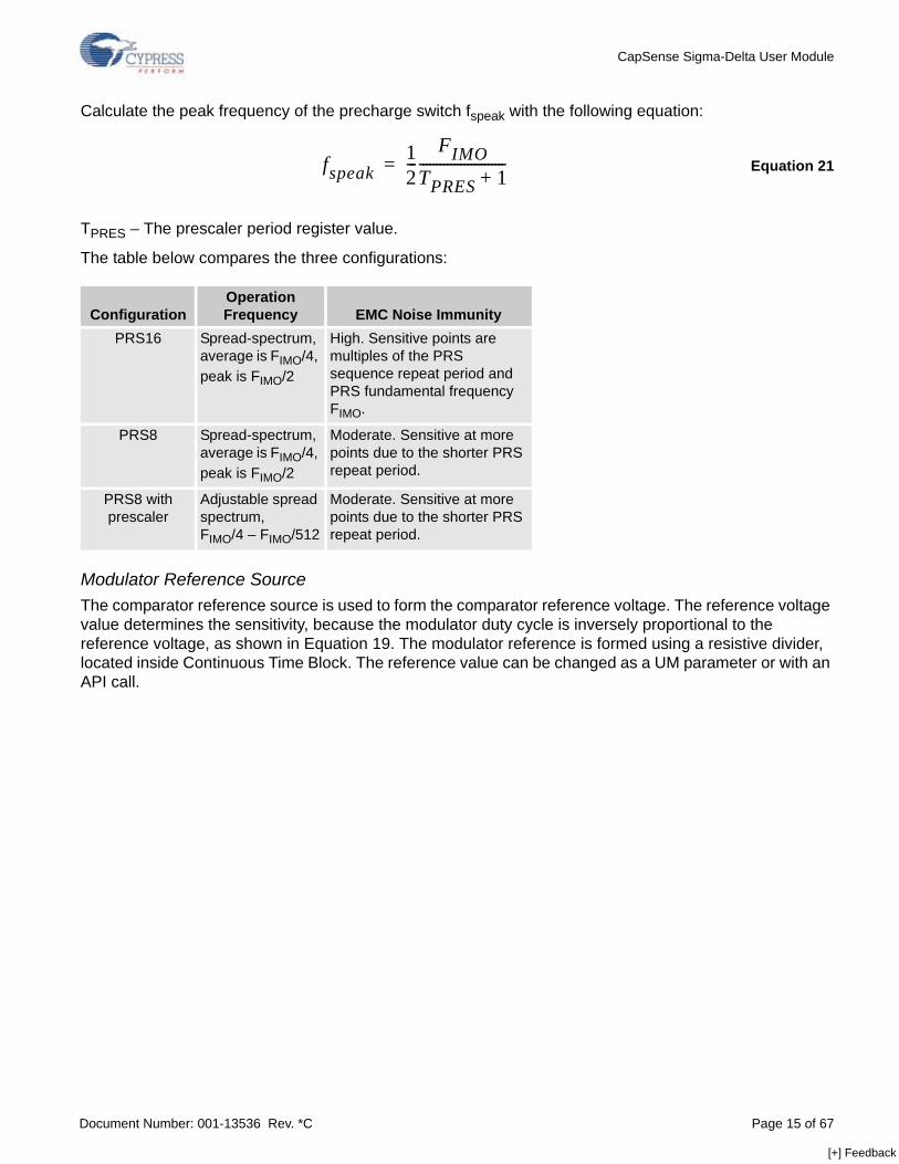
The table below compares the three configurations:
Modulator Reference SourceThe comparator reference source is used to form the comparator reference voltage. The reference voltage value determines the sensitivity, because the modulator duty cycle is inversely proportional to the reference voltage, as shown in Equation 19. The modulator reference is formed using a resistive divider, located inside Continuous Time Block. The reference value can be changed as a UM parameter or with an API call.
ConfigurationOperation Frequency EMC Noise Immunity
PRS16 Spread-spectrum, average is FIMO/4, peak is FIMO/2
High. Sensitive points are multiples of the PRS sequence repeat period and PRS fundamental frequency FIMO.
PRS8 Spread-spectrum, average is FIMO/4, peak is FIMO/2
Moderate. Sensitive at more points due to the shorter PRS repeat period.
PRS8 with prescaler
Adjustable spread spectrum,FIMO/4 – FIMO/512
Moderate. Sensitive at more points due to the shorter PRS repeat period.
fspeak12---
FIMOTPRES 1+-------------------------=
[+] Feedback
CapSense Sigma-Delta User Module
Document Number: 001-13536 Rev. *C Page 16 of 67
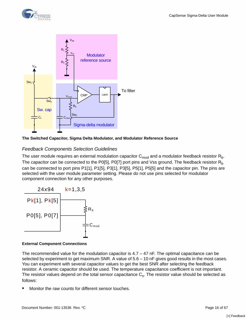
The Switched Capacitor, Sigma Delta Modulator, and Modulator Reference Source
Feedback Components Selection GuidelinesThe user module requires an external modulation capacitor Cmod and a modulator feedback resistor Rb. The capacitor can be connected to the P0[5], P0[7] port pins and Vss ground. The feedback resistor Rb can be connected to port pins P1[1], P1[5], P3[1], P3[5], P5[1], P5[5] and the capacitor pin. The pins are selected with the user module parameter setting. Please do not use pins selected for modulator component connection for any other purposes.
External Component Connections
The recommended value for the modulation capacitor is 4.7 – 47 nF. The optimal capacitance can be selected by experiment to get maximum SNR. A value of 5.6 – 10 nF gives good results in the most cases. You can experiment with several capacitor values to get the best SNR after selecting the feedback resistor. A ceramic capacitor should be used. The temperature capacitance coefficient is not important. The resistor values depend on the total sensor capacitance Cs. The resistor value should be selected as follows:
• Monitor the raw counts for different sensor touches.
Latch
Rb
CmodCx
Vdd
Sigma-delta modulator
Sw. cap
Sw1
Sw2
Sw3
VCmodCMP
Vref Modulator reference source
Vdd
R2
R1
To filter
Cmod
Rb
Pk[1], Pk[5]
P0[5], P0[7]
24x94 k=1,3,5
[+] Feedback
CapSense Sigma-Delta User Module
Document Number: 001-13536 Rev. *C Page 17 of 67
• Select a resistance value that provides maximum readings about 30% less than the full scale readings at the selected scanning resolution. The raw counts are increased when resistor values increase.
Typical values are 500Ω – 10 kΩ depending on sensor capacitance and precharge switch operation frequency. You can start with 2.0kΩ if you are using the CY3214 evaluation board.
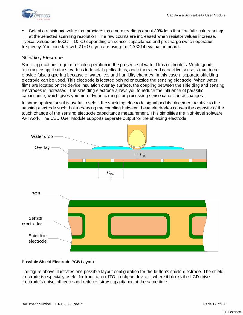
Shielding ElectrodeSome applications require reliable operation in the presence of water films or droplets. White goods, automotive applications, various industrial applications, and others need capacitive sensors that do not provide false triggering because of water, ice, and humidity changes. In this case a separate shielding electrode can be used. This electrode is located behind or outside the sensing electrode. When water films are located on the device insulation overlay surface, the coupling between the shielding and sensing electrodes is increased. The shielding electrode allows you to reduce the influence of parasitic capacitance, which gives you more dynamic range for processing sense capacitance changes. In some applications it is useful to select the shielding electrode signal and its placement relative to the sensing electrode such that increasing the coupling between these electrodes causes the opposite of the touch change of the sensing electrode capacitance measurement. This simplifies the high-level software API work. The CSD User Module supports separate output for the shielding electrode.
Possible Shield Electrode PCB Layout
The figure above illustrates one possible layout configuration for the button’s shield electrode. The shield electrode is especially useful for transparent ITO touchpad devices, where it blocks the LCD drive electrode’s noise influence and reduces stray capacitance at the same time.
Overlay
PCB
Water drop
Cx
Cpar
Sensor electrodes
Shielding electrode
[+] Feedback
CapSense Sigma-Delta User Module
Document Number: 001-13536 Rev. *C Page 18 of 67
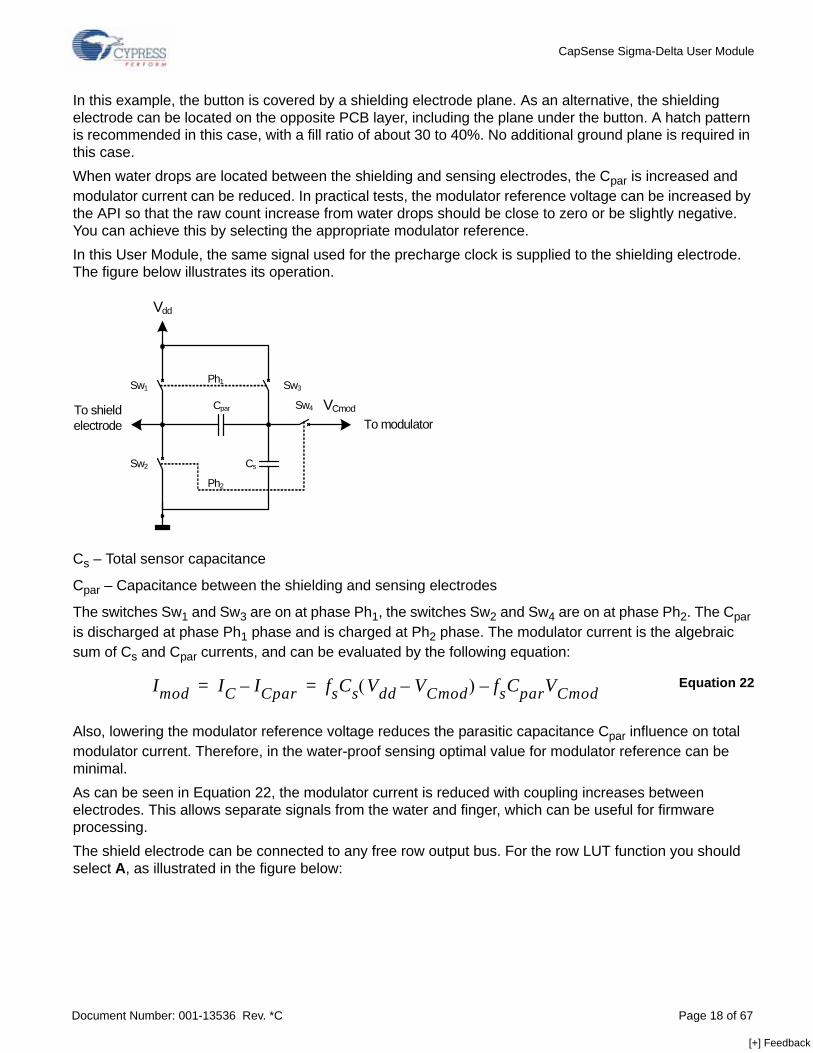
In this example, the button is covered by a shielding electrode plane. As an alternative, the shielding electrode can be located on the opposite PCB layer, including the plane under the button. A hatch pattern is recommended in this case, with a fill ratio of about 30 to 40%. No additional ground plane is required in this case.When water drops are located between the shielding and sensing electrodes, the Cpar is increased and modulator current can be reduced. In practical tests, the modulator reference voltage can be increased by the API so that the raw count increase from water drops should be close to zero or be slightly negative. You can achieve this by selecting the appropriate modulator reference.In this User Module, the same signal used for the precharge clock is supplied to the shielding electrode. The figure below illustrates its operation.
Cs – Total sensor capacitance
Cpar – Capacitance between the shielding and sensing electrodes
The switches Sw1 and Sw3 are on at phase Ph1, the switches Sw2 and Sw4 are on at phase Ph2. The Cpar is discharged at phase Ph1 phase and is charged at Ph2 phase. The modulator current is the algebraic sum of Cs and Cpar currents, and can be evaluated by the following equation:
Equation 22
Also, lowering the modulator reference voltage reduces the parasitic capacitance Cpar influence on total modulator current. Therefore, in the water-proof sensing optimal value for modulator reference can be minimal. As can be seen in Equation 22, the modulator current is reduced with coupling increases between electrodes. This allows separate signals from the water and finger, which can be useful for firmware processing. The shield electrode can be connected to any free row output bus. For the row LUT function you should select A, as illustrated in the figure below:
Cpar
Vdd
To modulator
Sw1
Sw2
Sw3
Sw4
Cs
Ph1
Ph2
To shield electrode
VCmod
Imod IC ICpar– fsCs Vdd VCmod–( ) fsCparVCmod–= =
[+] Feedback
CapSense Sigma-Delta User Module
Document Number: 001-13536 Rev. *C Page 19 of 67
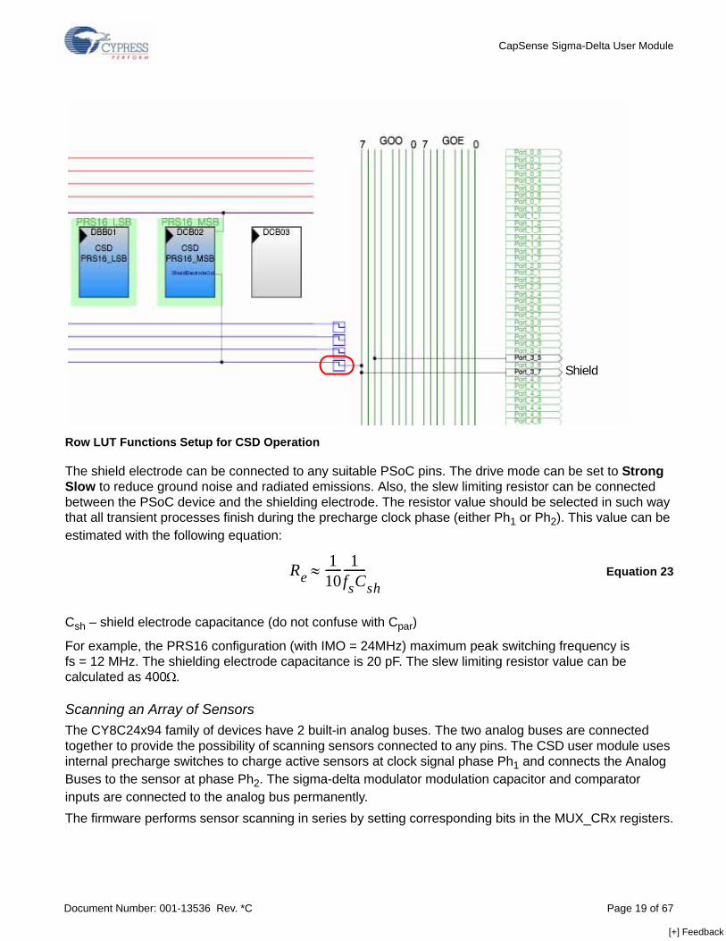
Row LUT Functions Setup for CSD Operation
The shield electrode can be connected to any suitable PSoC pins. The drive mode can be set to Strong Slow to reduce ground noise and radiated emissions. Also, the slew limiting resistor can be connected between the PSoC device and the shielding electrode. The resistor value should be selected in such way that all transient processes finish during the precharge clock phase (either Ph1 or Ph2). This value can be estimated with the following equation:
Equation 23
Csh – shield electrode capacitance (do not confuse with Cpar)
For example, the PRS16 configuration (with IMO = 24MHz) maximum peak switching frequency is fs = 12 MHz. The shielding electrode capacitance is 20 pF. The slew limiting resistor value can be calculated as 400Ω.
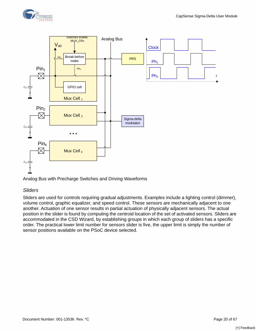
Scanning an Array of SensorsThe CY8C24x94 family of devices have 2 built-in analog buses. The two analog buses are connected together to provide the possibility of scanning sensors connected to any pins. The CSD user module uses internal precharge switches to charge active sensors at clock signal phase Ph1 and connects the Analog Buses to the sensor at phase Ph2. The sigma-delta modulator modulation capacitor and comparator inputs are connected to the analog bus permanently. The firmware performs sensor scanning in series by setting corresponding bits in the MUX_CRx registers.
Shield
Re110------ 1
fsC--------
sh≈
[+] Feedback
CapSense Sigma-Delta User Module
Document Number: 001-13536 Rev. *C Page 20 of 67
Analog Bus with Precharge Switches and Driving Waveforms
Sliders Sliders are used for controls requiring gradual adjustments. Examples include a lighting control (dimmer), volume control, graphic equalizer, and speed control. These sensors are mechanically adjacent to one another. Actuation of one sensor results in partial actuation of physically adjacent sensors. The actual position in the slider is found by computing the centroid location of the set of activated sensors. Sliders are accommodated in the CSD Wizard, by establishing groups in which each group of sliders has a specific order. The practical lower limit number for sensors slider is five, the upper limit is simply the number of sensor positions available on the PSoC device selected.
Vdd
Break-before make
Ph1
Ph2
GPIO cell
Pin1
Cx1
Pin2
Cx2
Switches enable, MUX_CRx
...
PRS
Analog Bus
Pink
Cxk
Mux Cell 1
Mux Cell 2
Mux Cell k
Sigma-delta modulator
t
Clock
Ph1
Ph2
[+] Feedback
CapSense Sigma-Delta User Module
Document Number: 001-13536 Rev. *C Page 21 of 67
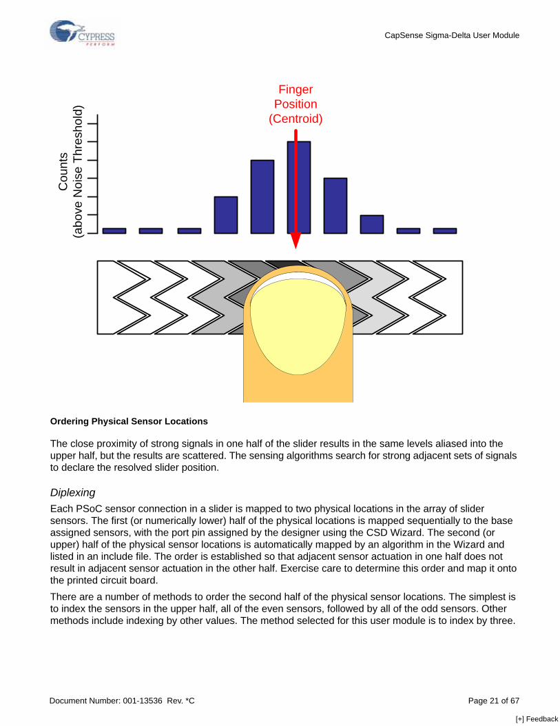
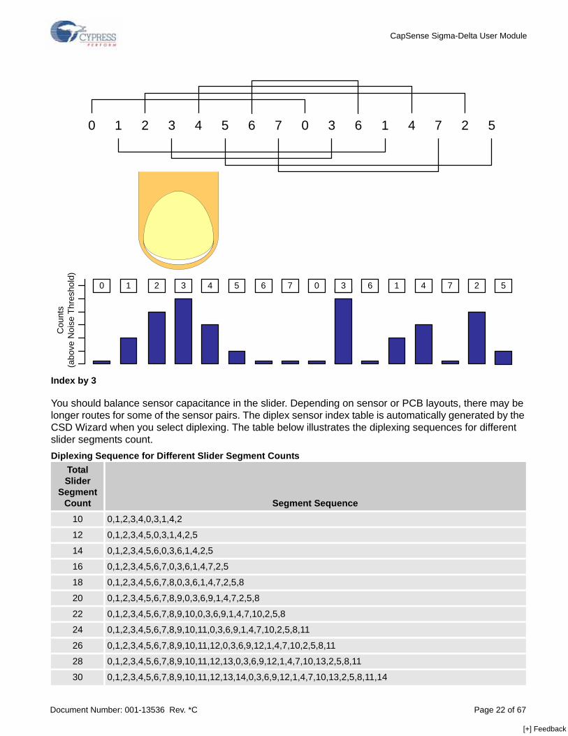
Ordering Physical Sensor Locations
The close proximity of strong signals in one half of the slider results in the same levels aliased into the upper half, but the results are scattered. The sensing algorithms search for strong adjacent sets of signals to declare the resolved slider position.
Diplexing Each PSoC sensor connection in a slider is mapped to two physical locations in the array of slider sensors. The first (or numerically lower) half of the physical locations is mapped sequentially to the base assigned sensors, with the port pin assigned by the designer using the CSD Wizard. The second (or upper) half of the physical sensor locations is automatically mapped by an algorithm in the Wizard and listed in an include file. The order is established so that adjacent sensor actuation in one half does not result in adjacent sensor actuation in the other half. Exercise care to determine this order and map it onto the printed circuit board. There are a number of methods to order the second half of the physical sensor locations. The simplest is to index the sensors in the upper half, all of the even sensors, followed by all of the odd sensors. Other methods include indexing by other values. The method selected for this user module is to index by three.
FingerPosition
(Centroid)
Cou
nts
(abo
ve N
oise
Thr
esho
ld)
[+] Feedback
CapSense Sigma-Delta User Module
Document Number: 001-13536 Rev. *C Page 22 of 67
Index by 3
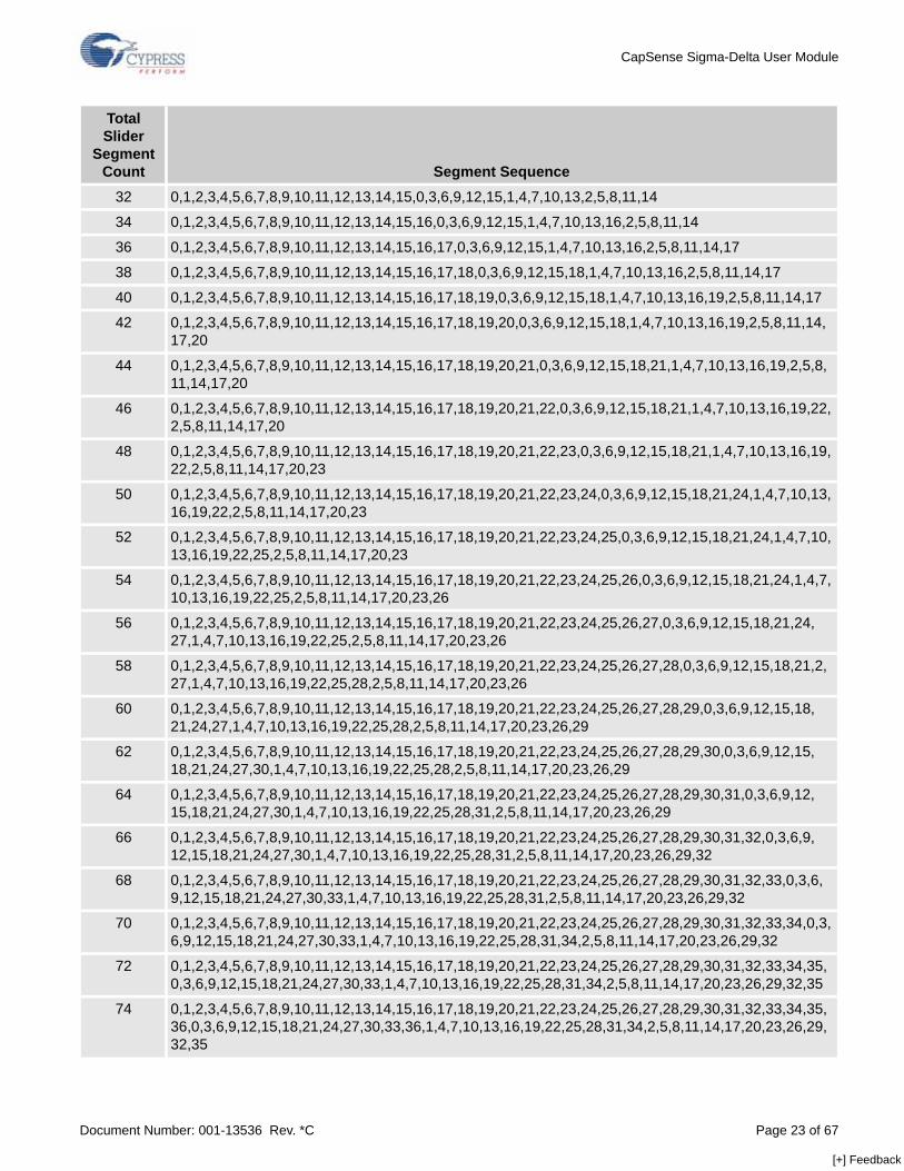
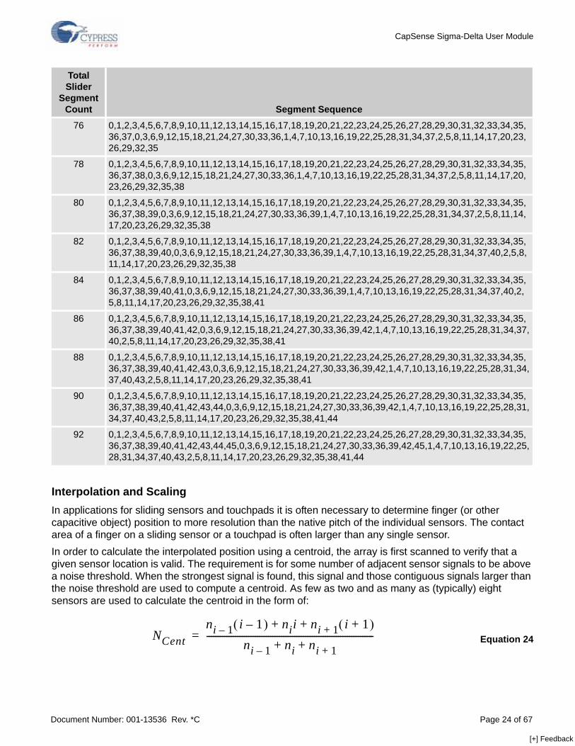
You should balance sensor capacitance in the slider. Depending on sensor or PCB layouts, there may be longer routes for some of the sensor pairs. The diplex sensor index table is automatically generated by the CSD Wizard when you select diplexing. The table below illustrates the diplexing sequences for different slider segments count. Diplexing Sequence for Different Slider Segment Counts
Total Slider
Segment Count Segment Sequence
10 0,1,2,3,4,0,3,1,4,2
12 0,1,2,3,4,5,0,3,1,4,2,5
14 0,1,2,3,4,5,6,0,3,6,1,4,2,5
16 0,1,2,3,4,5,6,7,0,3,6,1,4,7,2,5
18 0,1,2,3,4,5,6,7,8,0,3,6,1,4,7,2,5,8
20 0,1,2,3,4,5,6,7,8,9,0,3,6,9,1,4,7,2,5,8
22 0,1,2,3,4,5,6,7,8,9,10,0,3,6,9,1,4,7,10,2,5,8
24 0,1,2,3,4,5,6,7,8,9,10,11,0,3,6,9,1,4,7,10,2,5,8,11
26 0,1,2,3,4,5,6,7,8,9,10,11,12,0,3,6,9,12,1,4,7,10,2,5,8,11
28 0,1,2,3,4,5,6,7,8,9,10,11,12,13,0,3,6,9,12,1,4,7,10,13,2,5,8,11
30 0,1,2,3,4,5,6,7,8,9,10,11,12,13,14,0,3,6,9,12,1,4,7,10,13,2,5,8,11,14
2 3 4 5 6 7 0 3 6 1 4 7 2 510
5 6 72 3 4 010 1 4 73 6 2 5
Cou
nts
(abo
ve N
oise
Thr
esho
ld)
[+] Feedback
CapSense Sigma-Delta User Module
Document Number: 001-13536 Rev. *C Page 23 of 67
32 0,1,2,3,4,5,6,7,8,9,10,11,12,13,14,15,0,3,6,9,12,15,1,4,7,10,13,2,5,8,11,14
34 0,1,2,3,4,5,6,7,8,9,10,11,12,13,14,15,16,0,3,6,9,12,15,1,4,7,10,13,16,2,5,8,11,14
36 0,1,2,3,4,5,6,7,8,9,10,11,12,13,14,15,16,17,0,3,6,9,12,15,1,4,7,10,13,16,2,5,8,11,14,17
38 0,1,2,3,4,5,6,7,8,9,10,11,12,13,14,15,16,17,18,0,3,6,9,12,15,18,1,4,7,10,13,16,2,5,8,11,14,17
40 0,1,2,3,4,5,6,7,8,9,10,11,12,13,14,15,16,17,18,19,0,3,6,9,12,15,18,1,4,7,10,13,16,19,2,5,8,11,14,17
42 0,1,2,3,4,5,6,7,8,9,10,11,12,13,14,15,16,17,18,19,20,0,3,6,9,12,15,18,1,4,7,10,13,16,19,2,5,8,11,14,17,20
44 0,1,2,3,4,5,6,7,8,9,10,11,12,13,14,15,16,17,18,19,20,21,0,3,6,9,12,15,18,21,1,4,7,10,13,16,19,2,5,8,11,14,17,20
46 0,1,2,3,4,5,6,7,8,9,10,11,12,13,14,15,16,17,18,19,20,21,22,0,3,6,9,12,15,18,21,1,4,7,10,13,16,19,22,2,5,8,11,14,17,20
48 0,1,2,3,4,5,6,7,8,9,10,11,12,13,14,15,16,17,18,19,20,21,22,23,0,3,6,9,12,15,18,21,1,4,7,10,13,16,19,22,2,5,8,11,14,17,20,23
50 0,1,2,3,4,5,6,7,8,9,10,11,12,13,14,15,16,17,18,19,20,21,22,23,24,0,3,6,9,12,15,18,21,24,1,4,7,10,13,16,19,22,2,5,8,11,14,17,20,23
52 0,1,2,3,4,5,6,7,8,9,10,11,12,13,14,15,16,17,18,19,20,21,22,23,24,25,0,3,6,9,12,15,18,21,24,1,4,7,10,13,16,19,22,25,2,5,8,11,14,17,20,23
54 0,1,2,3,4,5,6,7,8,9,10,11,12,13,14,15,16,17,18,19,20,21,22,23,24,25,26,0,3,6,9,12,15,18,21,24,1,4,7,10,13,16,19,22,25,2,5,8,11,14,17,20,23,26
56 0,1,2,3,4,5,6,7,8,9,10,11,12,13,14,15,16,17,18,19,20,21,22,23,24,25,26,27,0,3,6,9,12,15,18,21,24, 27,1,4,7,10,13,16,19,22,25,2,5,8,11,14,17,20,23,26
58 0,1,2,3,4,5,6,7,8,9,10,11,12,13,14,15,16,17,18,19,20,21,22,23,24,25,26,27,28,0,3,6,9,12,15,18,21,2, 27,1,4,7,10,13,16,19,22,25,28,2,5,8,11,14,17,20,23,26
60 0,1,2,3,4,5,6,7,8,9,10,11,12,13,14,15,16,17,18,19,20,21,22,23,24,25,26,27,28,29,0,3,6,9,12,15,18, 21,24,27,1,4,7,10,13,16,19,22,25,28,2,5,8,11,14,17,20,23,26,29
62 0,1,2,3,4,5,6,7,8,9,10,11,12,13,14,15,16,17,18,19,20,21,22,23,24,25,26,27,28,29,30,0,3,6,9,12,15, 18,21,24,27,30,1,4,7,10,13,16,19,22,25,28,2,5,8,11,14,17,20,23,26,29
64 0,1,2,3,4,5,6,7,8,9,10,11,12,13,14,15,16,17,18,19,20,21,22,23,24,25,26,27,28,29,30,31,0,3,6,9,12, 15,18,21,24,27,30,1,4,7,10,13,16,19,22,25,28,31,2,5,8,11,14,17,20,23,26,29
66 0,1,2,3,4,5,6,7,8,9,10,11,12,13,14,15,16,17,18,19,20,21,22,23,24,25,26,27,28,29,30,31,32,0,3,6,9, 12,15,18,21,24,27,30,1,4,7,10,13,16,19,22,25,28,31,2,5,8,11,14,17,20,23,26,29,32
68 0,1,2,3,4,5,6,7,8,9,10,11,12,13,14,15,16,17,18,19,20,21,22,23,24,25,26,27,28,29,30,31,32,33,0,3,6, 9,12,15,18,21,24,27,30,33,1,4,7,10,13,16,19,22,25,28,31,2,5,8,11,14,17,20,23,26,29,32
70 0,1,2,3,4,5,6,7,8,9,10,11,12,13,14,15,16,17,18,19,20,21,22,23,24,25,26,27,28,29,30,31,32,33,34,0,3,6,9,12,15,18,21,24,27,30,33,1,4,7,10,13,16,19,22,25,28,31,34,2,5,8,11,14,17,20,23,26,29,32
72 0,1,2,3,4,5,6,7,8,9,10,11,12,13,14,15,16,17,18,19,20,21,22,23,24,25,26,27,28,29,30,31,32,33,34,35,0,3,6,9,12,15,18,21,24,27,30,33,1,4,7,10,13,16,19,22,25,28,31,34,2,5,8,11,14,17,20,23,26,29,32,35
74 0,1,2,3,4,5,6,7,8,9,10,11,12,13,14,15,16,17,18,19,20,21,22,23,24,25,26,27,28,29,30,31,32,33,34,35,36,0,3,6,9,12,15,18,21,24,27,30,33,36,1,4,7,10,13,16,19,22,25,28,31,34,2,5,8,11,14,17,20,23,26,29,32,35
Total Slider
Segment Count Segment Sequence
[+] Feedback
CapSense Sigma-Delta User Module
Document Number: 001-13536 Rev. *C Page 24 of 67
Interpolation and Scaling In applications for sliding sensors and touchpads it is often necessary to determine finger (or other capacitive object) position to more resolution than the native pitch of the individual sensors. The contact area of a finger on a sliding sensor or a touchpad is often larger than any single sensor. In order to calculate the interpolated position using a centroid, the array is first scanned to verify that a given sensor location is valid. The requirement is for some number of adjacent sensor signals to be above a noise threshold. When the strongest signal is found, this signal and those contiguous signals larger than the noise threshold are used to compute a centroid. As few as two and as many as (typically) eight sensors are used to calculate the centroid in the form of:
Equation 24
76 0,1,2,3,4,5,6,7,8,9,10,11,12,13,14,15,16,17,18,19,20,21,22,23,24,25,26,27,28,29,30,31,32,33,34,35,36,37,0,3,6,9,12,15,18,21,24,27,30,33,36,1,4,7,10,13,16,19,22,25,28,31,34,37,2,5,8,11,14,17,20,23,26,29,32,35
78 0,1,2,3,4,5,6,7,8,9,10,11,12,13,14,15,16,17,18,19,20,21,22,23,24,25,26,27,28,29,30,31,32,33,34,35,36,37,38,0,3,6,9,12,15,18,21,24,27,30,33,36,1,4,7,10,13,16,19,22,25,28,31,34,37,2,5,8,11,14,17,20,23,26,29,32,35,38
80 0,1,2,3,4,5,6,7,8,9,10,11,12,13,14,15,16,17,18,19,20,21,22,23,24,25,26,27,28,29,30,31,32,33,34,35,36,37,38,39,0,3,6,9,12,15,18,21,24,27,30,33,36,39,1,4,7,10,13,16,19,22,25,28,31,34,37,2,5,8,11,14,17,20,23,26,29,32,35,38
82 0,1,2,3,4,5,6,7,8,9,10,11,12,13,14,15,16,17,18,19,20,21,22,23,24,25,26,27,28,29,30,31,32,33,34,35,36,37,38,39,40,0,3,6,9,12,15,18,21,24,27,30,33,36,39,1,4,7,10,13,16,19,22,25,28,31,34,37,40,2,5,8,11,14,17,20,23,26,29,32,35,38
84 0,1,2,3,4,5,6,7,8,9,10,11,12,13,14,15,16,17,18,19,20,21,22,23,24,25,26,27,28,29,30,31,32,33,34,35,36,37,38,39,40,41,0,3,6,9,12,15,18,21,24,27,30,33,36,39,1,4,7,10,13,16,19,22,25,28,31,34,37,40,2, 5,8,11,14,17,20,23,26,29,32,35,38,41
86 0,1,2,3,4,5,6,7,8,9,10,11,12,13,14,15,16,17,18,19,20,21,22,23,24,25,26,27,28,29,30,31,32,33,34,35,36,37,38,39,40,41,42,0,3,6,9,12,15,18,21,24,27,30,33,36,39,42,1,4,7,10,13,16,19,22,25,28,31,34,37,40,2,5,8,11,14,17,20,23,26,29,32,35,38,41
88 0,1,2,3,4,5,6,7,8,9,10,11,12,13,14,15,16,17,18,19,20,21,22,23,24,25,26,27,28,29,30,31,32,33,34,35,36,37,38,39,40,41,42,43,0,3,6,9,12,15,18,21,24,27,30,33,36,39,42,1,4,7,10,13,16,19,22,25,28,31,34,37,40,43,2,5,8,11,14,17,20,23,26,29,32,35,38,41
90 0,1,2,3,4,5,6,7,8,9,10,11,12,13,14,15,16,17,18,19,20,21,22,23,24,25,26,27,28,29,30,31,32,33,34,35,36,37,38,39,40,41,42,43,44,0,3,6,9,12,15,18,21,24,27,30,33,36,39,42,1,4,7,10,13,16,19,22,25,28,31,34,37,40,43,2,5,8,11,14,17,20,23,26,29,32,35,38,41,44
92 0,1,2,3,4,5,6,7,8,9,10,11,12,13,14,15,16,17,18,19,20,21,22,23,24,25,26,27,28,29,30,31,32,33,34,35,36,37,38,39,40,41,42,43,44,45,0,3,6,9,12,15,18,21,24,27,30,33,36,39,42,45,1,4,7,10,13,16,19,22,25,28,31,34,37,40,43,2,5,8,11,14,17,20,23,26,29,32,35,38,41,44
Total Slider
Segment Count Segment Sequence
NCentni 1– i 1–( ) nii ni 1+ i 1+( )+ +
ni 1– ni ni 1++ +----------------------------------------------------------------------------=
[+] Feedback
CapSense Sigma-Delta User Module
Document Number: 001-13536 Rev. *C Page 25 of 67
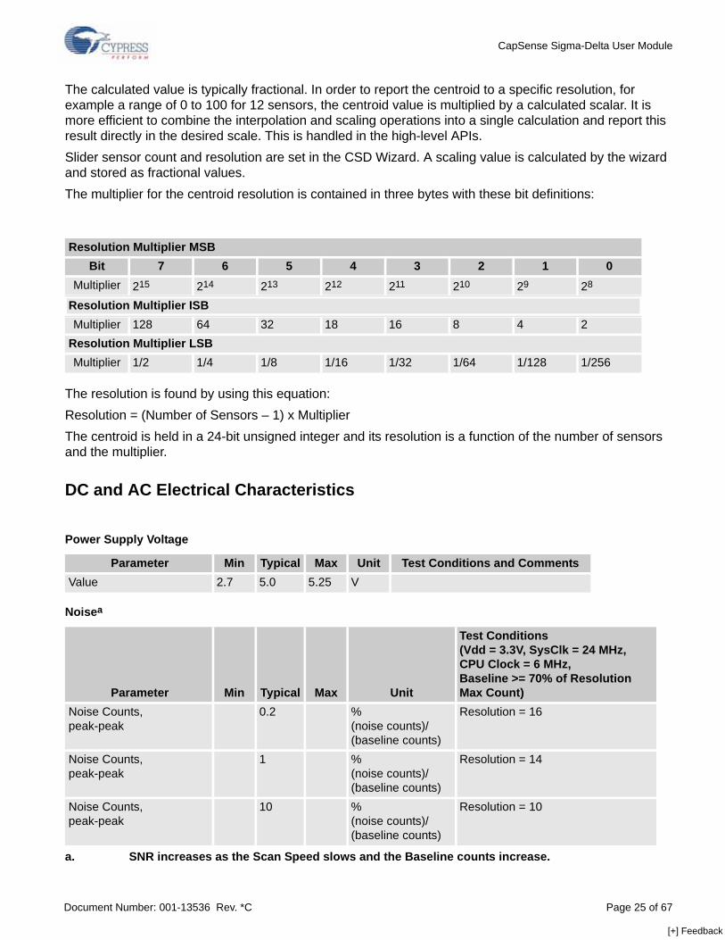
The calculated value is typically fractional. In order to report the centroid to a specific resolution, for example a range of 0 to 100 for 12 sensors, the centroid value is multiplied by a calculated scalar. It is more efficient to combine the interpolation and scaling operations into a single calculation and report this result directly in the desired scale. This is handled in the high-level APIs. Slider sensor count and resolution are set in the CSD Wizard. A scaling value is calculated by the wizard and stored as fractional values. The multiplier for the centroid resolution is contained in three bytes with these bit definitions:
The resolution is found by using this equation:Resolution = (Number of Sensors – 1) x MultiplierThe centroid is held in a 24-bit unsigned integer and its resolution is a function of the number of sensors and the multiplier.
DC and AC Electrical Characteristics
Resolution Multiplier MSBBit 7 6 5 4 3 2 1 0
Multiplier 215 214 213 212 211 210 29 28
Resolution Multiplier ISBMultiplier 128 64 32 18 16 8 4 2
Resolution Multiplier LSBMultiplier 1/2 1/4 1/8 1/16 1/32 1/64 1/128 1/256
Power Supply Voltage
Parameter Min Typical Max Unit Test Conditions and CommentsValue 2.7 5.0 5.25 V
Noisea
a. SNR increases as the Scan Speed slows and the Baseline counts increase.
Parameter Min Typical Max Unit
Test Conditions(Vdd = 3.3V, SysClk = 24 MHz,CPU Clock = 6 MHz,Baseline >= 70% of Resolution Max Count)
Noise Counts,peak-peak
0.2 %(noise counts)/(baseline counts)
Resolution = 16
Noise Counts,peak-peak
1 %(noise counts)/(baseline counts)
Resolution = 14
Noise Counts,peak-peak
10 %(noise counts)/(baseline counts)
Resolution = 10
[+] Feedback

CapSense Sigma-Delta User Module
Document Number: 001-13536 Rev. *C Page 26 of 67
Characterization GraphsTest conditions: The resolution is set to 12 bits, data was collected using the CY3214, rev. A evaluation board. See the notes for more details.
Power Consumption
Supply Voltage Min Typ Max Unit Test Conditions and CommentsActive Current 10 mA Average current during scan, 8 sensors Standby Current 250 μA Scanning Speed = Ultra Fast, Resolution = 9 100 ms
report rate, 8 sensors 1.6 mA Scanning Speed = Fast, Resolution = 12 100 ms report
rate, 8 sensors Sleep/Wake Current 10 μA 1s report rate, 1 sensor
[+] Feedback
CapSense Sigma-Delta User Module
Document Number: 001-13536 Rev. *C Page 27 of 67
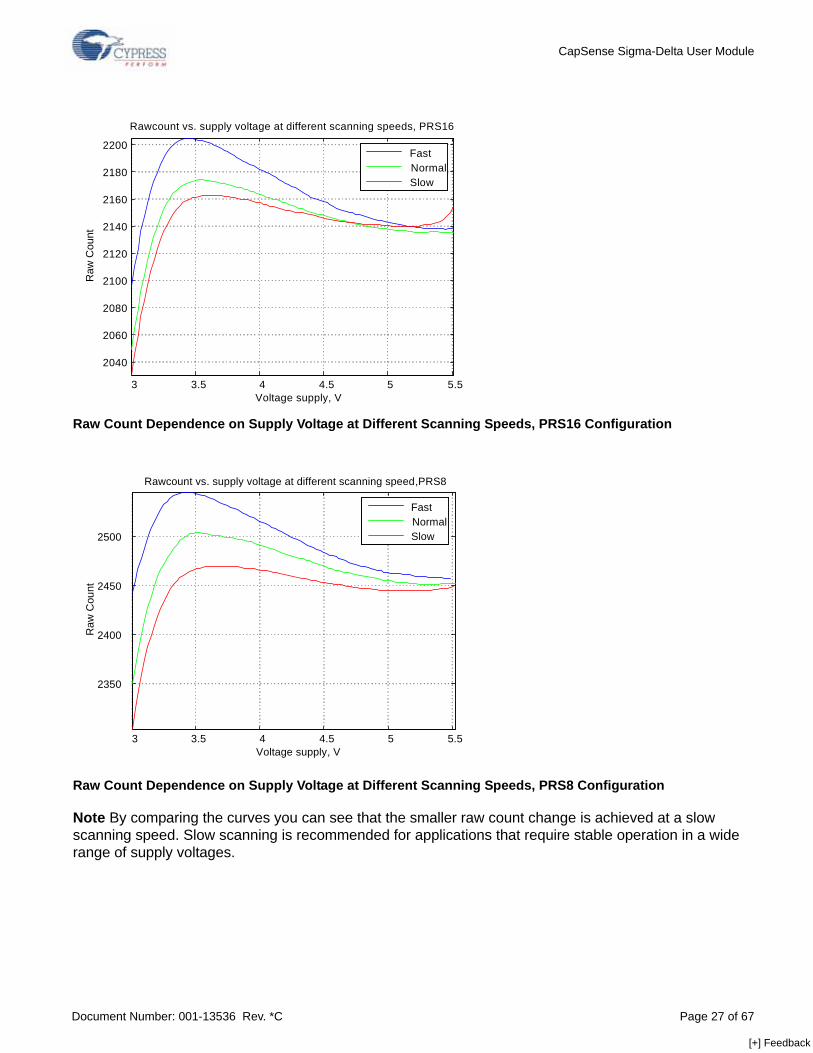
Raw Count Dependence on Supply Voltage at Different Scanning Speeds, PRS16 Configuration
Raw Count Dependence on Supply Voltage at Different Scanning Speeds, PRS8 Configuration
Note By comparing the curves you can see that the smaller raw count change is achieved at a slow scanning speed. Slow scanning is recommended for applications that require stable operation in a wide range of supply voltages.
3 3.5 4 4.5 5 5.5
2040
2060
2080
2100
2120
2140
2160
2180
2200
Voltage supply, V
Raw
Cou
nt
Rawcount vs. supply voltage at different scanning speeds, PRS16
FastNormalSlow
3 3.5 4 4.5 5 5.5
2350
2400
2450
2500
Voltage supply, V
Raw
Cou
nt
Rawcount vs. supply voltage at different scanning speed,PRS8
FastNormalSlow
[+] Feedback
CapSense Sigma-Delta User Module
Document Number: 001-13536 Rev. *C Page 28 of 67
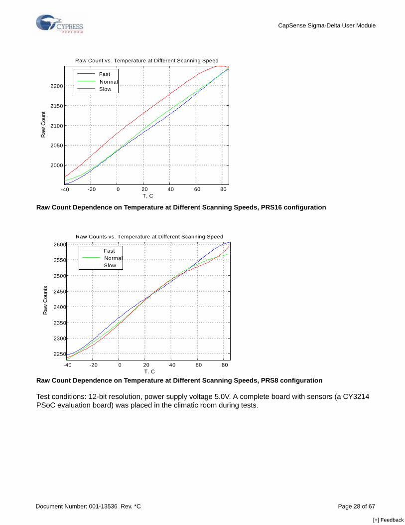
Raw Count Dependence on Temperature at Different Scanning Speeds, PRS16 configuration
Raw Count Dependence on Temperature at Different Scanning Speeds, PRS8 configuration
Test conditions: 12-bit resolution, power supply voltage 5.0V. A complete board with sensors (a CY3214 PSoC evaluation board) was placed in the climatic room during tests.
-40 -20 0 20 40 60 80
2000
2050
2100
2150
2200
T, C
Raw
Cou
nt
Raw Count vs. Temperature at Different Scanning Speed
FastNormalSlow
-40 -20 0 20 40 60 80
2250
2300
2350
2400
2450
2500
2550
2600
T, C
Raw
Cou
nts
Raw Counts vs. Temperature at Different Scanning Speed
FastNormalSlow
[+] Feedback
CapSense Sigma-Delta User Module
Document Number: 001-13536 Rev. *C Page 29 of 67
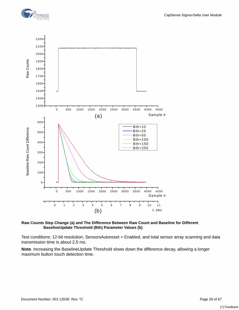
Raw Counts Step Change (a) and The Difference Between Raw Count and Baseline for Different BaselineUpdate Threshold (Bth) Parameter Values (b)
Test conditions: 12-bit resolution, SensorsAutoreset = Enabled, and total sensor array scanning and data transmission time is about 2.5 ms.Note. Increasing the BaselineUpdate Threshold slows down the difference decay, allowing a longer maximum button touch detection time.
0 500 1000 1500 2000 2500 3000 3500 4000 4500
0
100
200
300
400
500
600
Bas
elin
e-R
aw C
ount
Diff
eren
ce
Sam ple #
0 500 1000 1500 2000 2500 3000 3500 4000 45001300
1400
1500
1600
1700
1800
1900
2000
2100
2200
Raw
Cou
nts
Sam ple #
0 1 2 3 4 5 6 7 8 9 10 11
t, sec
B th=10 B th=25 B th=50 B th=100 B th=150 B th=255
(a)
(b)
[+] Feedback
CapSense Sigma-Delta User Module
Document Number: 001-13536 Rev. *C Page 30 of 67
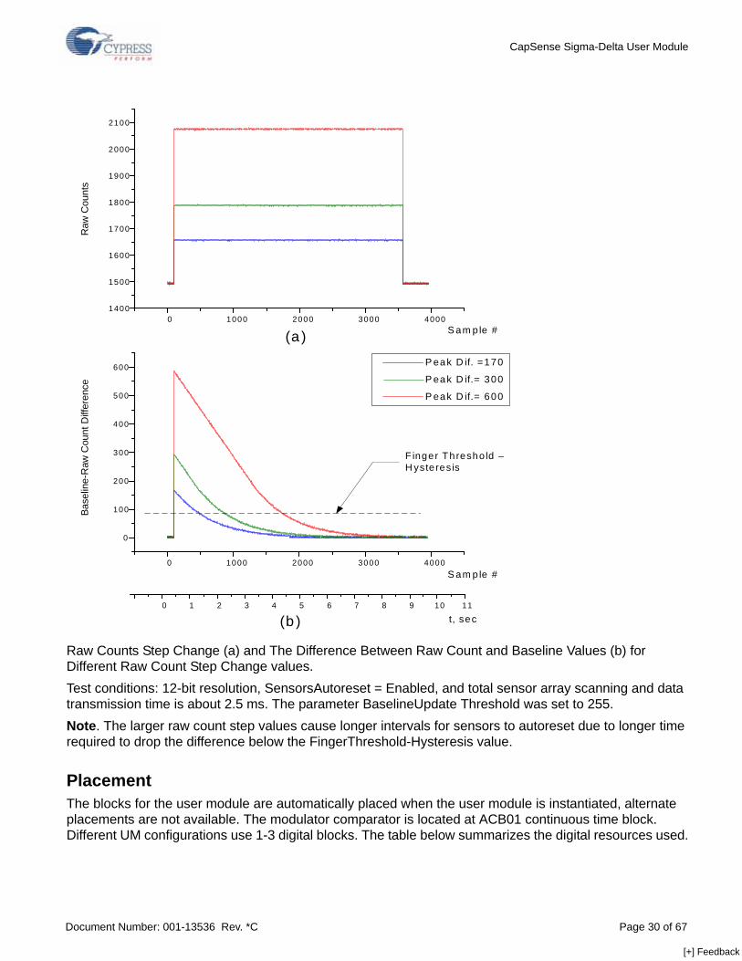
Raw Counts Step Change (a) and The Difference Between Raw Count and Baseline Values (b) for Different Raw Count Step Change values. Test conditions: 12-bit resolution, SensorsAutoreset = Enabled, and total sensor array scanning and data transmission time is about 2.5 ms. The parameter BaselineUpdate Threshold was set to 255.Note. The larger raw count step values cause longer intervals for sensors to autoreset due to longer time required to drop the difference below the FingerThreshold-Hysteresis value.
PlacementThe blocks for the user module are automatically placed when the user module is instantiated, alternate placements are not available. The modulator comparator is located at ACB01 continuous time block. Different UM configurations use 1-3 digital blocks. The table below summarizes the digital resources used.
Base
line-
Raw
Cou
nt D
iffer
ence
S am p le #
Raw
Cou
nts
0 1 2 3 4 5 6 7 8 9 10 11
t, sec
(a )
(b )
0 1000 2000 3000 4000
0
100
200
300
400
500
600 P eak D if. =170
P eak D if.= 300
P eak D if.= 600
0 1000 2000 3000 40001400
1500
1600
1700
1800
1900
2000
2100
S am ple #
F inger Thresho ld –H ysteresis
[+] Feedback
CapSense Sigma-Delta User Module
Document Number: 001-13536 Rev. *C Page 31 of 67
The unused analog and digital blocks are available for your own purposes. All UM configurations use the hardware decimator.User modules that consume specific pin resources, including the LCD and I2CHW, must be placed before establishing port pin connections for the CSD User Module. The configuration selections are reflected in the Wizard when it is opened.Avoid P1[0] and P1[1] when placing capacitive sensor connections. These pins are used for programming the part and may have excess routing capacitance affecting sensor sensitivity and noise.
Wizard
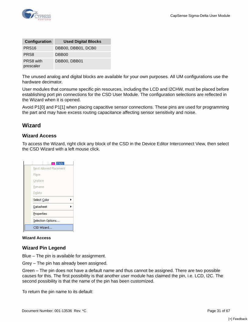
Wizard Access To access the Wizard, right click any block of the CSD in the Device Editor Interconnect View, then select the CSD Wizard with a left mouse click.
Wizard Access
Wizard Pin Legend Blue – The pin is available for assignment. Grey – The pin has already been assigned. Green – The pin does not have a default name and thus cannot be assigned. There are two possible causes for this. The first possibility is that another user module has claimed the pin, i.e. LCD, I2C. The second possibility is that the name of the pin has been customized.
To return the pin name to its default:
Configuration Used Digital BlocksPRS16 DBB00, DBB01, DCB0PRS8 DBB00PRS8 with prescaler
DBB00, DBB01
[+] Feedback
CapSense Sigma-Delta User Module
Document Number: 001-13536 Rev. *C Page 32 of 67
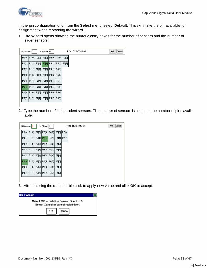
In the pin configuration grid, from the Select menu, select Default. This will make the pin available for assignment when reopening the wizard. 1. The Wizard opens showing the numeric entry boxes for the number of sensors and the number of
slider sensors.
2. Type the number of independent sensors. The number of sensors is limited to the number of pins avail-able.
3. After entering the data, double click to apply new value and click OK to accept.
[+] Feedback
CapSense Sigma-Delta User Module
Document Number: 001-13536 Rev. *C Page 33 of 67
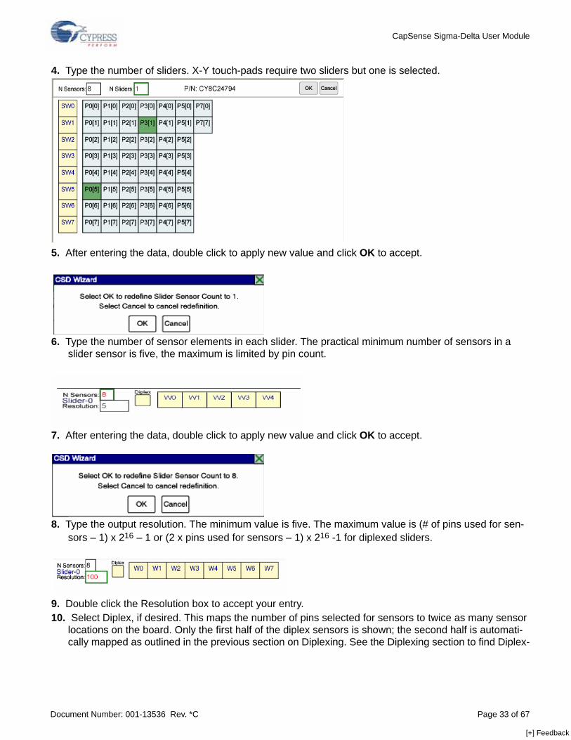
4. Type the number of sliders. X-Y touch-pads require two sliders but one is selected.
5. After entering the data, double click to apply new value and click OK to accept.
6. Type the number of sensor elements in each slider. The practical minimum number of sensors in a slider sensor is five, the maximum is limited by pin count.
7. After entering the data, double click to apply new value and click OK to accept.
8. Type the output resolution. The minimum value is five. The maximum value is (# of pins used for sen-sors – 1) x 216 – 1 or (2 x pins used for sensors – 1) x 216 -1 for diplexed sliders.
9. Double click the Resolution box to accept your entry.10. Select Diplex, if desired. This maps the number of pins selected for sensors to twice as many sensor
locations on the board. Only the first half of the diplex sensors is shown; the second half is automati-cally mapped as outlined in the previous section on Diplexing. See the Diplexing section to find Diplex-
[+] Feedback
CapSense Sigma-Delta User Module
Document Number: 001-13536 Rev. *C Page 34 of 67
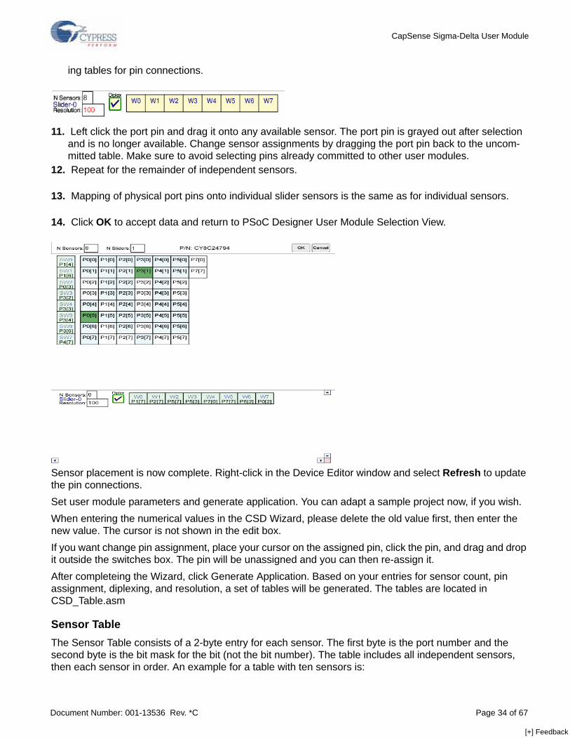
ing tables for pin connections.
11. Left click the port pin and drag it onto any available sensor. The port pin is grayed out after selection and is no longer available. Change sensor assignments by dragging the port pin back to the uncom-mitted table. Make sure to avoid selecting pins already committed to other user modules.
12. Repeat for the remainder of independent sensors.
13. Mapping of physical port pins onto individual slider sensors is the same as for individual sensors.
14. Click OK to accept data and return to PSoC Designer User Module Selection View.
Sensor placement is now complete. Right-click in the Device Editor window and select Refresh to update the pin connections.Set user module parameters and generate application. You can adapt a sample project now, if you wish. When entering the numerical values in the CSD Wizard, please delete the old value first, then enter the new value. The cursor is not shown in the edit box.If you want change pin assignment, place your cursor on the assigned pin, click the pin, and drag and drop it outside the switches box. The pin will be unassigned and you can then re-assign it.After completeing the Wizard, click Generate Application. Based on your entries for sensor count, pin assignment, diplexing, and resolution, a set of tables will be generated. The tables are located in CSD_Table.asm
Sensor Table The Sensor Table consists of a 2-byte entry for each sensor. The first byte is the port number and the second byte is the bit mask for the bit (not the bit number). The table includes all independent sensors, then each sensor in order. An example for a table with ten sensors is:
[+] Feedback
CapSense Sigma-Delta User Module
Document Number: 001-13536 Rev. *C Page 35 of 67
CSD_Sensor_Table:_CSD_Sensor_Table: dw 0x0001 // Port 0 Bit 0 dw 0x0002 // Port 0 Bit 1 dw 0x0004 // Port 0 Bit 2 dw 0x0008 // Port 0 Bit 3 dw 0x0010 // Port 0 Bit 4 dw 0x0101 // Port 1 Bit 0 dw 0x0102 // Port 1 Bit 1 dw 0x0104 // Port 1 Bit 2 dw 0x0108 // Port 1 Bit 3 dw 0x0110 // Port 1 Bit 4
This table is used by CSD_wGetPortPin() routine.
Group Table The Group Table defines each of the groups of button sensors or sliders. There is one entry for each slider plus one for the free button sensors. The first entry is always the free sensors. Each entry is six bytes. The first byte is the index in the Sensor Table where the group starts. The second byte is how many sensors are in that group. The third byte signifies whether the slider is diplexed or not (4 is diplexed, 0 is not diplexed). The fourth, fifth, and sixth bytes are the fixed point multiplier that the slider's calculated centroid will be multiplied by to achieve the resolution desired in the CSD wizard.
CSD_1_Group_Table:_CSD_1_Group_Table:; Group Table:; Origin Count Diplex? DivBtwSw(wholeMSB, wholeLSB, fractByte) db 0x0, 0x5, 0x00, 0x00, 0x00, 0x00 ; Buttons db 0x5, 0x5, 0x3, 0x0, 0x0, 0x71 ; Slider 1
Diplex Table Diplex table scan order data is produced for a group when it is a slider and is also diplexed. Otherwise a label is created but no data is placed. The table consists of two parts: sensor mapping for each slider, and a reference for each separate slider to its table. A typical example for an five sensor slider is shown below.
DiplexTable_0:; This group is not a diplexed sliderDiplexTable_1: db 0,1,2,3,4,0,3,1,4,2 // 5 switch slider
CSD_1_Diplex_Table:_CSD_1_Diplex_Table: db >DiplexTable_0, <DiplexTable_0 db >DiplexTable_1, <DiplexTable_1
Parameters
Finger ThresholdThis threshold is used to determine the state of each button sensor. If any sensor is active, the bIsAnySensorActive() function returns a 1. If all sensors are off, the bIsAnySensorActive() function returns a 0.
[+] Feedback
CapSense Sigma-Delta User Module
Document Number: 001-13536 Rev. *C Page 36 of 67
The finger detection threshold values apply to all sensors and sliders. For individual sensors (not contained in a slider group), these thresholds are variable and provided in the baBtnFThreshold[] array. The SetDefaultFingerThresholds() function may be used to set the thresholds to the default value set in the Device Editor. To adjust the sensitivity for individual sensors, change the baBtnFThreshold[] value for each sensor. (The size of this byte array is equal to the count of implemented individual sensors.) Possible values range from 5 to 255.
Noise ThresholdFor individual sensors, count values above this threshold do not update the baseline. For slider sensors, count values below this threshold are not counted in the calculation of the centroid. Possible values are 5 to 255.
BaselineUpdate ThresholdWhen the new raw count value is above the current baseline and the difference is below the noise threshold (with the Sensors Autoreset parameter set to Disabled), the difference between the current baseline and the raw count is accumulated into what could be thought of as a bucket. When the bucket fills, the baseline is incremented by some value and the bucket is emptied. This parameter sets the threshold that the bucket must reach for the baseline to increment. Possible values are 0 to 255. Larger parameter values yield slower baseline update speeds. If you need more frequent baseline updates, decreases this parameter.
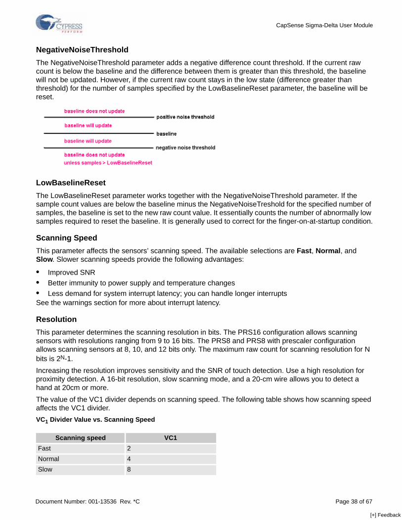
NegativeNoiseThresholdThe NegativeNoiseThreshold parameter adds a negative difference count threshold. If the current raw count is below the baseline and the difference between them is greater than this threshold, the baseline will not be updated. However, if the current raw count stays in the low state (difference greater than threshold) for the number of samples specified by the LowBaselineReset parameter, the baseline will be reset.
LowBaselineResetThe LowBaselineReset parameter works together with the NegativeNoiseThreshold parameter. If the sample count values are below the baseline minus the NegativeNoiseTreshold for the specified number of samples, the baseline is set to the new raw count value. It essentially counts the number of abnormally low samples required to reset the baseline. It is generally used to correct for the finger-on-at-startup condition.
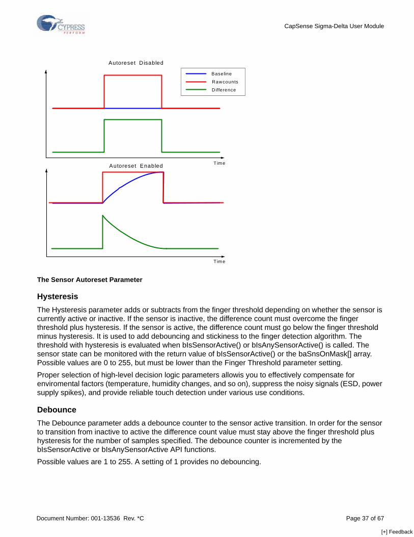
Sensors AutoresetThis parameter determines whether the baseline is updated at all times or only when the signal difference is below the Noise Threshold. When set to Enabled the baseline is updated constantly. This setting limits the maximum time duration of the sensor (typical values are 5 – 10s), but it prevents the sensors from permanently turning on when the raw count suddenly rises without anything touching the sensor. This sudden rise can be caused by a large power supply voltage fluctuation, a high-energy RF noise source, or a very quick temperature change.When the parameter is set to Disabled the baseline is updated only when raw count and baseline difference is below the Noise Threshold parameter. You should leave this parameter Enabled unless there is a demand to keep the sensors in the on state for a long time.The figure below illustrates this parameter’s influence on the baseline update.
[+] Feedback
CapSense Sigma-Delta User Module
Document Number: 001-13536 Rev. *C Page 37 of 67
The Sensor Autoreset Parameter
HysteresisThe Hysteresis parameter adds or subtracts from the finger threshold depending on whether the sensor is currently active or inactive. If the sensor is inactive, the difference count must overcome the finger threshold plus hysteresis. If the sensor is active, the difference count must go below the finger threshold minus hysteresis. It is used to add debouncing and stickiness to the finger detection algorithm. The threshold with hysteresis is evaluated when bIsSensorActive() or bIsAnySensorActive() is called. The sensor state can be monitored with the return value of bIsSensorActive() or the baSnsOnMask[] array. Possible values are 0 to 255, but must be lower than the Finger Threshold parameter setting.Proper selection of high-level decision logic parameters allowis you to effectively compensate for enviromental factors (temperature, humidity changes, and so on), suppress the noisy signals (ESD, power supply spikes), and provide reliable touch detection under various use conditions.
DebounceThe Debounce parameter adds a debounce counter to the sensor active transition. In order for the sensor to transition from inactive to active the difference count value must stay above the finger threshold plus hysteresis for the number of samples specified. The debounce counter is incremented by the bIsSensorActive or bIsAnySensorActive API functions.Possible values are 1 to 255. A setting of 1 provides no debouncing.
Autoreset D isabled
Baseline
Rawcounts
D ifference
Autoreset Enabled
Time
Time
[+] Feedback
CapSense Sigma-Delta User Module
Document Number: 001-13536 Rev. *C Page 38 of 67
NegativeNoiseThresholdThe NegativeNoiseThreshold parameter adds a negative difference count threshold. If the current raw count is below the baseline and the difference between them is greater than this threshold, the baseline will not be updated. However, if the current raw count stays in the low state (difference greater than threshold) for the number of samples specified by the LowBaselineReset parameter, the baseline will be reset.
LowBaselineResetThe LowBaselineReset parameter works together with the NegativeNoiseThreshold parameter. If the sample count values are below the baseline minus the NegativeNoiseTreshold for the specified number of samples, the baseline is set to the new raw count value. It essentially counts the number of abnormally low samples required to reset the baseline. It is generally used to correct for the finger-on-at-startup condition.
Scanning SpeedThis parameter affects the sensors’ scanning speed. The available selections are Fast, Normal, and Slow. Slower scanning speeds provide the following advantages:
• Improved SNR• Better immunity to power supply and temperature changes• Less demand for system interrupt latency; you can handle longer interruptsSee the warnings section for more about interrupt latency.
ResolutionThis parameter determines the scanning resolution in bits. The PRS16 configuration allows scanning sensors with resolutions ranging from 9 to 16 bits. The PRS8 and PRS8 with prescaler configuration allows scanning sensors at 8, 10, and 12 bits only. The maximum raw count for scanning resolution for N bits is 2N-1. Increasing the resolution improves sensitivity and the SNR of touch detection. Use a high resolution for proximity detection. A 16-bit resolution, slow scanning mode, and a 20-cm wire allows you to detect a hand at 20cm or more.The value of the VC1 divider depends on scanning speed. The following table shows how scanning speed affects the VC1 divider.VC1 Divider Value vs. Scanning Speed
Scanning speed VC1Fast 2Normal 4Slow 8
[+] Feedback
CapSense Sigma-Delta User Module
Document Number: 001-13536 Rev. *C Page 39 of 67
.
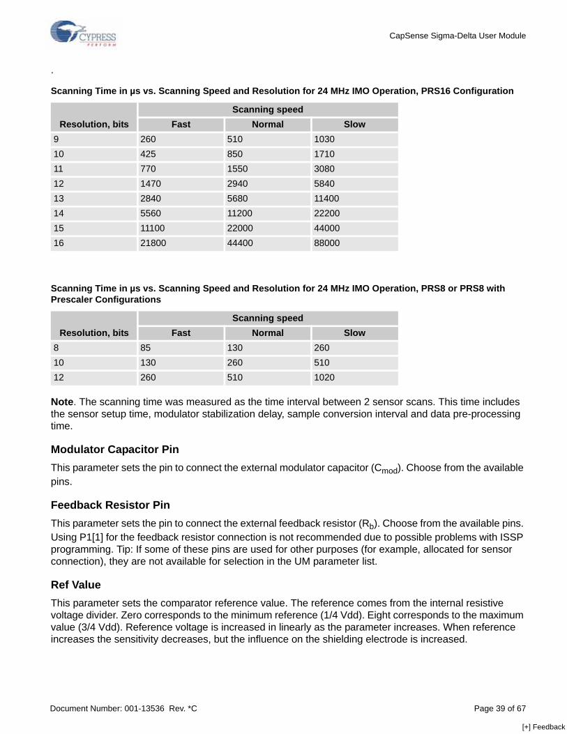
Note. The scanning time was measured as the time interval between 2 sensor scans. This time includes the sensor setup time, modulator stabilization delay, sample conversion interval and data pre-processing time.
Modulator Capacitor PinThis parameter sets the pin to connect the external modulator capacitor (Cmod). Choose from the available pins.
Feedback Resistor PinThis parameter sets the pin to connect the external feedback resistor (Rb). Choose from the available pins. Using P1[1] for the feedback resistor connection is not recommended due to possible problems with ISSP programming. Tip: If some of these pins are used for other purposes (for example, allocated for sensor connection), they are not available for selection in the UM parameter list.
Ref ValueThis parameter sets the comparator reference value. The reference comes from the internal resistive voltage divider. Zero corresponds to the minimum reference (1/4 Vdd). Eight corresponds to the maximum value (3/4 Vdd). Reference voltage is increased in linearly as the parameter increases. When reference increases the sensitivity decreases, but the influence on the shielding electrode is increased.
Scanning Time in µs vs. Scanning Speed and Resolution for 24 MHz IMO Operation, PRS16 Configuration
Resolution, bitsScanning speed
Fast Normal Slow9 260 510 103010 425 850 171011 770 1550 308012 1470 2940 584013 2840 5680 1140014 5560 11200 2220015 11100 22000 4400016 21800 44400 88000
Scanning Time in µs vs. Scanning Speed and Resolution for 24 MHz IMO Operation, PRS8 or PRS8 with Prescaler Configurations
Resolution, bitsScanning speed
Fast Normal Slow8 85 130 26010 130 260 51012 260 510 1020
[+] Feedback
CapSense Sigma-Delta User Module
Document Number: 001-13536 Rev. *C Page 40 of 67
If the design has sensors with noticeable capacitance differences (for example, sensors with different sized squares), you can balance raw counts by setting a higher reference for the sensors with larger capacitance using an API function.
Prescaler PeriodThis parameter sets the prescaler period register and determines the precharge switch output frequency. This parameter is available for PRS8 configuration with prescaler only. The prescaler period values can range from 1 to 255.
The recommended values are 2n-1 to obtain the maximum signal to noise ratio (SNR).
• 1• 3• 7• 15• 31• 63• 127• 255 Other values can result in more noise, especially at low resolution and high scan speed.
PRS PolynomialThis parameter sets the PRS polynomial in the PRS8 and PRS8 with prescaler configurations. There are two selection options:
• Short – The short polynomial setting yields better SNR, but due to the shorter repeat period, the end device can be more susceptible to external noise sources.
• Long – The long polynomial setting yields worse SNR, but the device is more robust against noise sig-nals.
ShieldElectrodeOutThe shielding electrode signal source can be selected from one of the free digital row buses (Row_0_Output_0 - Row_0_Output_3). The chosen route has signal to any of three pins. Set the selected Row LUT Function to A.
Application Programming InterfaceThe Application Programming Interface (API) functions are provided as part of the user module to allow you to deal with the module at a higher level. This section specifies the interface to each function together with related constants provided by the include files.Note ** In this, as in all user module APIs, the values of the A and X register may be altered by calling an API function. It is the responsibility of the calling function to preserve the values of A and X before the call if those values are required after the call. This "registers are volatile" policy was selected for efficiency reasons and has been in force since version 1.0 of PSoC Designer. The C compiler automatically takes care of this requirement. Assembly language programmers must also ensure their code observes the policy. Though some user module API function may leave A and X unchanged, there is no guarantee they will do so in the future.
[+] Feedback
CapSense Sigma-Delta User Module
Document Number: 001-13536 Rev. *C Page 41 of 67
Entry Points are supplied to initialize the CSD, start it sampling, and stop the CSD. In all cases the instance name of the module replaces the CSD prefix shown in the following entry points. Failure to use the correct instance name is a common cause of syntax errors. API functions use different global arrays. You should not alter these arrays manually. You can inspect these values for debugging purposes, however. For example, you can use a charting tool to display the contents of the arrays. There several global arrays:
• CSD_waSnsBaseline[]• CSD_waSnsResult[]• CSD_waSnsDiff[]• CSD_baSnsOnMask[]
CSD_waSnsBaseline[] – This is an integer array that contains the baseline data of each sensor. The array size is equal to the sensor count. The CSD_waSnsBaseline[] array is updated by these functions:
• CSD_UpdateAllBaselines(); • CSD_UpdateSensorBaseline(); • CSD_InitializeBaselines(). CSD_waSnsResult[] – This is an integer array that contains the raw data of each sensor. The array size is equal to the sensor count. The CSD_waSnsResult[] data is updated by these functions:
• CSD_ScanSensor(); • CSD_ScanAllSensors().CSD_waSnsDiff [] – This is an integer array that contains the difference between the raw data and the baseline data of each sensor. The array size is equal to the sensor count.CSD_baSnsOnMask[] – This is a byte array that holds the sensor on or off state (for buttons or sliders). CSD_baSnsOnMask[0] contains the masked bits for sensors 0 through 7 (sensor 0 is bit 0, sensor 1 is bit 1). CSD_baSnsOnMask[1] contains the masked bits for sensors 8 through 15 (if they are needed), and so on. This byte array contains as many elements as are necessary to contain all the placed sensors. The value of a bit is 1 if the button is on and 0 if the button is off. The CSD_baSnsOnMask[] data is updated by CSD_blsSensorActive(BYTE bSensnor) function or CSD_bIsAnySensorActive() routines.
CSD_Start Description:
Initializes registers and starts the user module. This function should be called prior to calling any other user module functions.
C Prototype: void CSD_Start()
Assembly: call CSD_Start
Parameters: None
Return Value: None
Side Effects: **
[+] Feedback
CapSense Sigma-Delta User Module
Document Number: 001-13536 Rev. *C Page 42 of 67
CSD_Stop Description:
Stops the sensor scanner, disables internal interrupts, and calls CSD_ClearSensors() to reset all sen-sors to an inactive state.
C Prototype: void CSD_Stop()
Assembly: call CSD_Stop
Parameters: None
Return Value: None
Side Effects: **
CSD_ScanSensorDescription:
Scans the selected sensor. Each sensor has a unique number within the sensor array. This number is assigned by the CSD Wizard in sequence. Sw0 is sensor 0, Sw1 is sensor 1, and so on.
C Prototype:void CSD_ScanSensor(BYTE bSensor);
Assembly:mov A, bSensorcall CSD_ScanSensor
Parameters: A => Sensor Number
Return Value: None
Side Effects**
CSD_ScanAllSensorsDescription:
Scans all of the configured sensors by calling CSD_ScanSensor() for each sensor index.C Prototype:
void CSD_ScanAllSensors();
Assembly:call CSD_ScanAllSensors
Parameters: None
Return Value: None
Side Effects**
[+] Feedback
CapSense Sigma-Delta User Module
Document Number: 001-13536 Rev. *C Page 43 of 67
CSD_UpdateSensorBaselineDescription:
The historical count value, calculated independently for each sensor, is called the sensor's baseline. This baseline is updated using the Bucket Method.The Bucket Method uses the following algorithm.1. Each time CSD_UpdateSensorBaseline() is called, a difference count is calculated by subtracting the previous baseline from the raw count value. This difference is stored in the CSD_waSnsDiff[] array and is provided to you.2. If Sensors Autoreset is disabled, each time CSD_UpdateSensorBaseline() is called the difference count is compared to the noise threshold. If the difference is below the noise threshold, it is accumu-lated into a virtual bucket. If the difference is above the noise threshold, the bucket is not updated.
If Sensors Autoreset is enabled, the difference is accumulated into a virtual bucket regardless of the noise threshold parameter.3. Once the accumulated difference counts in the virtual bucket has reached the BaselineUpdateTh-reshold, the baseline is incremented by one and the bucket is reset to 0.4. If the difference count is below the noise threshold, the value held in the waSnsDiff[] array is reset to 0. Therefore, this array does not contain elements with values greater than 0 but below the NoiseTh-reshold.
C Prototype:void CSD_UpdateSensorBaseline(BYTE bSensor)
Assembly:mov A, bSensorcall CSD_UpdateSensorBaseline
Parameter: A => Sensor Number
Return Value:None
Side Effects:**
CSD_UpdateAllBaselinesDescription:
Uses the CSD_bUpdateSensorBaseline() function to update the baselines for all sensorsC Prototype:
void CSD_UpdateAllBaselines()
Assembly:call CSD_UpdateAllBaselines
Parameters:None
Return Value:None
Side Effects:**
[+] Feedback
CapSense Sigma-Delta User Module
Document Number: 001-13536 Rev. *C Page 44 of 67
CSD_bIsSensorActive Description:
Checks the difference count array for the given sensor compared to its finger threshold. Hysteresis is taken into account. The Hysteresis value is added or subtracted from the finger threshold based on whether the sensor is currently on. If it is active, the threshold is lowered. If it is inactive, the threshold is raised. This function also updates the sensor's bit in the CSD_baSnsOnMask[] array.
C Prototype:BYTE CSD_bIsSensorActive(BYTE bSensor)
Assembly:mov A, bSensorcall CSD_bIsSensorActive
Parameters:bSensor A => Sensor Number
Return Value:Return value of 1 if active, 0 if not activeA => 1 – Selected sensor is active, 0 – Selected sensor is not active.
Side Effects:**
CSD_bIsAnySensorActive Description:
Checks the difference count array for all sensors compared to their finger threshold. Calls CSD_bIsSensorActive() for each sensor so the CSD_baSnsOnMask[] array is up to date after calling this function.
C Prototype:BYTE CSD_bIsAnySensorActive()
Assembly:call CSD_bIsAnySensorActive
Parameters:None
Return Value:Return value of 1 if active, 0 if not activeA => 1 – One or more sensors are active, 0 – No sensors are active.
Side Effects:**
CSD_wGetCentroidPosDescription:
Checks a difference array for a centroid. If one exists, the offset and length are stored in temporary variables and the centroid position is calculated to the resolution specified in the CSD Wizard. This function is available only if slider is defined by the CSD Wizard.
C Prototype:WORD CSD_wGetCentroidPos(BYTE bSnsGroup)
[+] Feedback
CapSense Sigma-Delta User Module
Document Number: 001-13536 Rev. *C Page 45 of 67
Assembly:mov A, bSnsGroupcall CSD_wGetCentroidPos
Parameters:bSnsGroup A => Group NumberThis parameter is a reference to a specific group of sensors used as a slider. Group 0 is for buttons. Sliders are contained in group 1 and higher.
Return Value:Position value of the slider, LSB in A and MSB in X.
Side Effects:This routine modifies the difference counts by subtracting the noise threshold value. The routine should be called only once after each scan to avoid getting negative difference values. If your applica-tion monitors difference count signals, call this routine after difference count data transmission.If any slider sensor is active, the function returns values from zero to the Resolution value set in the CSD Wizard. If no sensors are active, the function returns –1 (FFFFh). If an error occurs during execu-tion of the centroid/diplexing algorithm, the function returns –1 (FFFFh). You can use the CSD_blsSensorActive() routine to determine which slider segments are touched, if required.Note: If noise counts on the slider segments are greater than the noise threshold, this subroutine may generate a false centroid result. The noise threshold should be set carefully (high enough above the noise level) so that noise will not generate a false centroid.
CSD_InitializeSensorBaseline Description:
Loads the CSD_waSnsBaseline[bSensor] array element with an initial value by scanning the selected sensor. The raw count value is copied in to the baseline array element for the selected sensor. This function can be used for resetting the baseline of an individual sensor.
C Prototype:void CSD_InitializeSensorBaseline(BYTE bSensor)
Assembly:mov A, bSensorcall CSD_InitializeSensorBaseline
Parameters:A => Sensor Number
Return Value:None
Side Effects:**
CSD_InitializeBaselines Description:
Loads the CSD_waSnsBaseline[] array with initial values by scanning each sensor. The raw count val-ues are copied in to baseline array for each sensor.
C Prototype:void CSD_InitializeBaselines()
Assembly:call CSD_InitializeBaselines
[+] Feedback

CapSense Sigma-Delta User Module
Document Number: 001-13536 Rev. *C Page 46 of 67
Parameters:None
Return Value:None
Side Effects:**
CSD_SetDefaultFingerThresholds Description:
Loads the CSD_baBtnFThreshold[] array with the FingerThreshold parameter value. This function must be called prior to scanning if the CSD_baBtnFThreshold[] array is not manually loaded with cus-tom values.
C Prototype:void CSD_SetDefaultFingerThresholds()
Assembly:call CSD_SetDefaultFingerThresholds
Parameters:None
Return Value:None
Side Effects:**
CSD_SetScanModeDescription:
Sets scanning speed and resolution. This function can be called at runtime to change the scanning speed and resolution. The function overwrites the user module parameter settings. This function is effective when some sensors need to be scanned with different scanning speed and resolution, for example, regular buttons and a proximity detector. The regular buttons can be scanned with 9-bit res-olution and 300 μs scan time. The proximity detector can be scanned less often with 16-bit resolution and scanning time of more than 12 ms for long-range detection. This function can be used in conjunc-tion with CSD_ScanSensor() function.
C Prototype: void CSD_SetScanMode(BYTE bSpeed, BYTE bResolution);
Assembly:mov A, bSpeedmov X, bResolutioncall CSD_SetScanMode
Parameters:bSpeedbResolution
Return Value:None
Side Effects:**
[+] Feedback
CapSense Sigma-Delta User Module
Document Number: 001-13536 Rev. *C Page 47 of 67
CSD_SetRefValueDescription:
Sets scanning reference value. Valid only when reference is supplied from the analog modulator (ASE11 in the Reference parameter) or from externally filtered PWM/PRSPWM signals. Accepted val-ues are 0..8. Value 0 corresponds to the minimum reference voltage that provides the maximum sensi-tivity. The value 8 sets the maximum reference voltage and results in lower sensitivity. This function can be used in conjunction with CSD_ScanSensor().
C Prototype: void CSD_SetRefValue(BYTE bRefValue);
Assembly: mov A, bRefValuecall CSD_SetRefValue
Parameters: bRefValue - sets the scanning reference vale. Accepted values are 0..8.
Return Value: None
Side Effects: **
CSD_ClearSensors Description:
Clears all sensors to the non-sampling state by sequentially calling CSD_wGetPortPin() and CSD_DisableSensor() for each of the sensors.
C Prototype: void CSD_ClearSensors()
Assembly: call CSD_ClearSensors
Parameters: None
Return Value: None
Side Effects: **
CSD_wReadSensor Description:
Returns the key Raw scan value in A (LSB) and X (MSB). C Prototype:
WORD CSD_wReadSensor(BYTE bSensor)
Assembly: mov A, bSensor call CSD_wReadSensor
Parameters: A => Sensor Number
[+] Feedback
CapSense Sigma-Delta User Module
Document Number: 001-13536 Rev. *C Page 48 of 67
Return Value: Scan value of sensor, LSB in A and MSB in X.
Side Effects: **
CSD_wGetPortPin Description: Returns the port number and pin mask for a given sensor. The passed parameter indexes and selects the data from the CSD_Sensor_Table[]. The return value can be passed to the CSD_EnableSensor(), CSD_DisableSensor().
C Prototype: WORD CSD_wGetPortPin(BYTE bSensorNum)
Assembly: mov A, bSensorNumber call CSD_wGetPortPin
Parameters: bSensorNumber – The range is 0 to (n – 1) where n is the total of the number of sensors set in the CSD Wizard plus the number of sensors included in sliders. The sensor number is used by CSD_wGetPortPin() to determine port and bit mask for the selected active sensor.
Return Value: A => Sensor Bitmap X => Port Number
Side Effects: **
CSD_EnableSensor Description:
Configures the selected sensor to measure during the next measurement cycle. The port and sensor can be selected using the CSD_wGetPortPin() function, with the port number and sensor bitmask loaded into X and A, respectively. Drive modes are modified to place the selected port and pin into Analog High-Z mode and to enable the correct Analog Mux Bus input. This also enables the compara-tor function.
C Prototype: void CSD_EnableSensor(BYTE bMask, BYTE bPort)
Assembly: mov X, bPort mov A, bMask call CSD_EnableSensor
Parameters: A => Sensor Bitmap X => Port Number
Return Value: None
Side Effects: **
[+] Feedback
CapSense Sigma-Delta User Module
Document Number: 001-13536 Rev. *C Page 49 of 67
CSD_DisableSensor Description:
Disables the sensor selected by the CSD_wGetPortPin() function. The drive mode is changed to Strong (001) and set to zero. This effectively grounds the sensor. The connection from the port pin to the AnalogMuxBus is turned off. The function parameters are returned by CSD_wGetPortPin() func-tion.
C Prototype: void CSD_DisableSensor(BYTE bMask, BYTE bPort)
Assembly: mov X, bPort mov A, bMask call CSD_DisableSensor
Parameters: A => Sensor Bitmap X => Port Number
Return Value: None
Side Effects: **
Sample CodeExample 1. This code starts the user module and continuously scans the sensors. The communication section can be used to communicate values to a PC charting tool.
//------------------------------------------------------------------------// Sample C code for the CSD module// Scanning all sensors continuously//------------------------------------------------------------------------
#include <m8c.h> // part specific constants and macros#include "PSoCAPI.h" // PSoC API definitions for all User Modules
void main(){ M8C_EnableGInt; CSD_Start(); CSD_InitializeBaselines() ; //scan all sensors first time, init baseline CSD_SetDefaultFingerThresholds() ; // // Loop Forever // while (1) { CSD_ScanAllSensors(); //scan all sensors in array (buttons and sliders) CSD_UpdateAllBaselines(); //Update all baseline levels;
//detect if any sensor is pressedif(CSD_bIsAnySensorActive()){
// Add user code here to proceed the sensor touching}
// now we are ready to send all status variables to chart program // communication here
[+] Feedback
CapSense Sigma-Delta User Module
Document Number: 001-13536 Rev. *C Page 50 of 67
// // OUTPUT CSD_waSnsResult[x] <- Raw Counts // OUTPUT CSD_waSnsDiff[x] <- Difference // OUTPUT CSD_waSnsBaseline[x] <- Baseline // OUTPUT CSD_baSnsOnMask[x] <- Sensor On/Off } }
Example 2.The code below demonstrates the ability to connect the several sensors in parallel and scan them at same time by calling the CSD_ScanSensor() function. This sample is useful when you need to detect sensors touches without separating which sensor has been touched. You can use this for device wake up detection and to minimize scanning time to save battery energy. If a wakeup touch is detected, you can return each of the sensors to conventional scanning individually.
//------------------------------------------------------------------------// Sample C code for the CSD module// Scan several sensors in parallel//------------------------------------------------------------------------
#include <m8c.h> // part specific constants and macros#include "PSoCAPI.h" // PSoC API definitions for all User Modules
void main(){ M8C_EnableGInt;
CSD_Start(); CSD_SetDefaultFingerThresholds();
// Enable the sensor connected to P1[4] CSD_EnableSensor(0x10, 1); // Enable the sensor connected to P1[6] CSD_EnableSensor(0x40, 1); // Enable the sensor connected to P3[0] CSD_EnableSensor(0x01, 3);
// Initialize baseline for sensor number "3" CSD_InitializeSensorBaseline(3);
while (1) { // Scan continuously sensor number "3" which is connected //in parallel to the enabled above sensors CSD_ScanSensor(3); CSD_UpdateSensorBaseline(3); if(CSD_bIsSensorActive(3)){
// Add user code here to proceed the buttons pressing } }}
Example 3. The example below demonstrates the ability to scan different sensors with different scanning parameters using the CSD_SetScanMode() function. Useful when need to performs buttons touch detection and proximity detection. The buttons are scanned with low resolution to reduce the scan time, the proximity is scanned with higher resolution to get maximum sensitivity. You can adapt this code to scan proximity less frequently and only when no button touch is detected.
//------------------------------------------------------------------------
[+] Feedback
CapSense Sigma-Delta User Module
Document Number: 001-13536 Rev. *C Page 51 of 67
// Sample C code for the CSD module// Scanning sensors with different scanning speed and resolution//------------------------------------------------------------------------
#include <m8c.h> // part specific constants and macros#include "PSoCAPI.h" // PSoC API definitions for all User Modules
void main(){
M8C_EnableGInt;
CSD_Start(); CSD_SetDefaultFingerThresholds();
// Set Fast, 9-bit resolution mode for baseline calculations CSD_SetScanMode(1, 9);
// Initialize baselines for all of the sensors which operate in // Fast mode and 9-bit resolution
CSD_InitializeSensorBaseline(0); CSD_InitializeSensorBaseline(1); CSD_InitializeSensorBaseline(2);
// Set Slow, 14-bit resolution mode for baseline calculations CSD_SetScanMode(3, 14); // Initialize baselines for all of the sensors which operate in
// Slow mode and 14-bit resolution CSD_InitializeSensorBaseline(3);
while (1) { // Set Fast, 9-bit resolution mode for the following buttons CSD_SetScanMode(1, 9); // Scan sensor number "0" CSD_ScanSensor(0); // Scan sensor number "1" CSD_ScanSensor(1); // Scan sensor number "2" CSD_ScanSensor(2);
// Set Slow, 14-bit resolution mode for the following sensor CSD_SetScanMode(3, 14); // Scan sensor number "3" CSD_ScanSensor(3);
CSD_UpdateAllBaselines(); //detect if any sensor is pressed if(CSD_bIsAnySensorActive()){ // Add user code here to proceed the buttons pressing } }}
Example 4. The example below demonstrates the ability to set the different Finger Threshold levels for each sensor. Useful when different sensors are placed on different locations and some sensors are more sensitive than others.
//------------------------------------------------------------------------// Sample C code for the CSD module
[+] Feedback
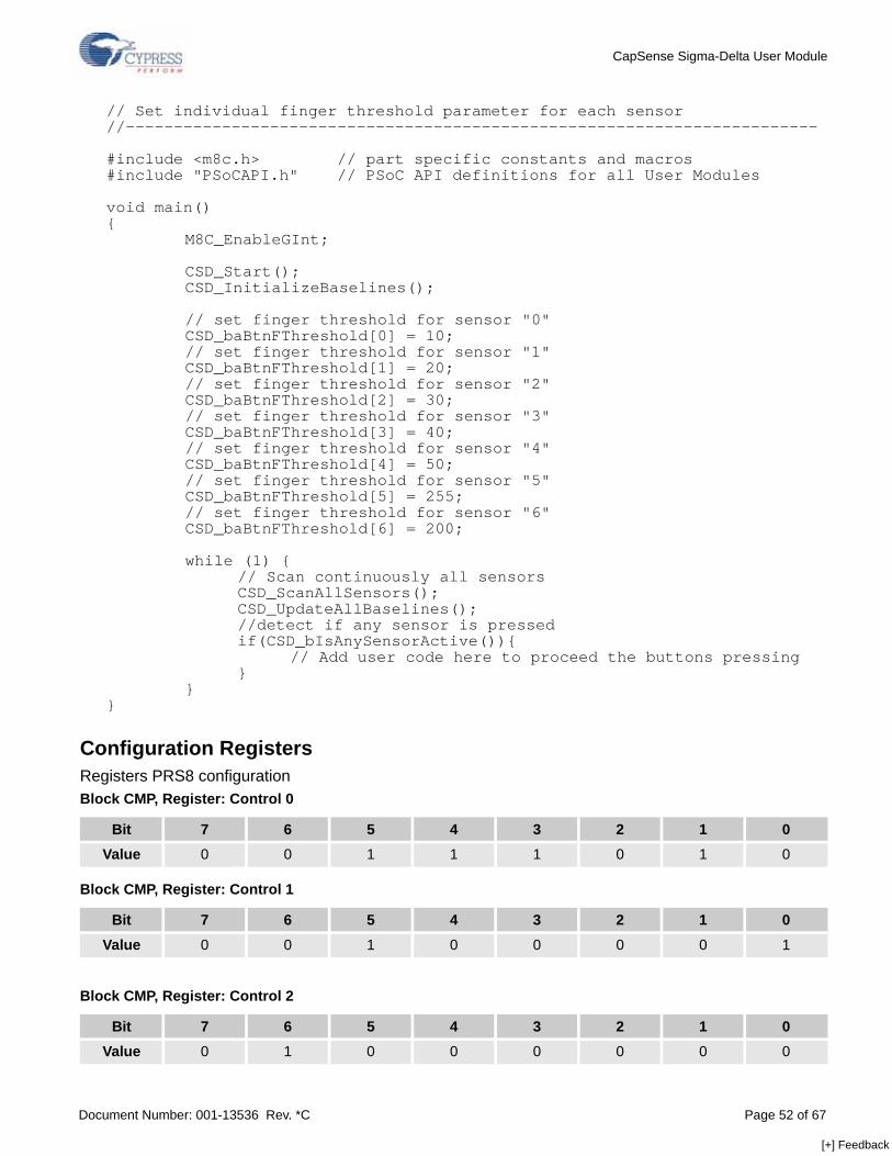
CapSense Sigma-Delta User Module
Document Number: 001-13536 Rev. *C Page 52 of 67
// Set individual finger threshold parameter for each sensor//------------------------------------------------------------------------
#include <m8c.h> // part specific constants and macros#include "PSoCAPI.h" // PSoC API definitions for all User Modules
void main(){
M8C_EnableGInt;
CSD_Start();CSD_InitializeBaselines();
// set finger threshold for sensor "0"CSD_baBtnFThreshold[0] = 10;// set finger threshold for sensor "1"CSD_baBtnFThreshold[1] = 20;// set finger threshold for sensor "2"CSD_baBtnFThreshold[2] = 30;// set finger threshold for sensor "3"CSD_baBtnFThreshold[3] = 40;// set finger threshold for sensor "4"CSD_baBtnFThreshold[4] = 50;// set finger threshold for sensor "5"CSD_baBtnFThreshold[5] = 255;// set finger threshold for sensor "6"CSD_baBtnFThreshold[6] = 200;
while (1) {// Scan continuously all sensorsCSD_ScanAllSensors();CSD_UpdateAllBaselines();//detect if any sensor is pressedif(CSD_bIsAnySensorActive()){
// Add user code here to proceed the buttons pressing}
}}
Configuration RegistersRegisters PRS8 configurationBlock CMP, Register: Control 0
Bit 7 6 5 4 3 2 1 0Value 0 0 1 1 1 0 1 0
Block CMP, Register: Control 1
Bit 7 6 5 4 3 2 1 0Value 0 0 1 0 0 0 0 1
Block CMP, Register: Control 2
Bit 7 6 5 4 3 2 1 0Value 0 1 0 0 0 0 0 0
[+] Feedback
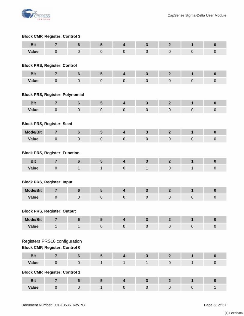
CapSense Sigma-Delta User Module
Document Number: 001-13536 Rev. *C Page 53 of 67
Registers PRS16 configuration
Block CMP, Register: Control 3
Bit 7 6 5 4 3 2 1 0Value 0 0 0 0 0 0 0 0
Block PRS, Register: Control
Bit 7 6 5 4 3 2 1 0Value 0 0 0 0 0 0 0 0
Block PRS, Register: Polynomial
Bit 7 6 5 4 3 2 1 0Value 0 0 0 0 0 0 0 0
Block PRS, Register: Seed
Mode/Bit 7 6 5 4 3 2 1 0Value 0 0 0 0 0 0 0 0
Block PRS, Register: Function
Bit 7 6 5 4 3 2 1 0Value 0 1 1 0 1 0 1 0
Block PRS, Register: Input
Mode/Bit 7 6 5 4 3 2 1 0Value 0 0 0 0 0 0 0 0
Block PRS, Register: Output
Mode/Bit 7 6 5 4 3 2 1 0Value 1 1 0 0 0 0 0 0
Block CMP, Register: Control 0
Bit 7 6 5 4 3 2 1 0Value 0 0 1 1 1 0 1 0
Block CMP, Register: Control 1
Bit 7 6 5 4 3 2 1 0Value 0 0 1 0 0 0 0 1
[+] Feedback
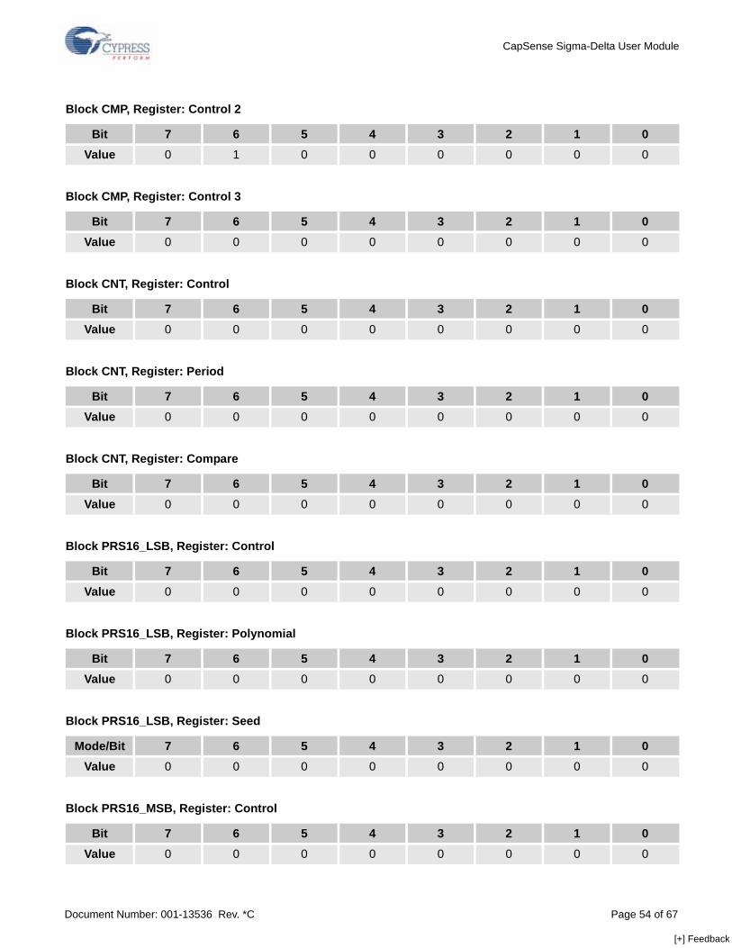
CapSense Sigma-Delta User Module
Document Number: 001-13536 Rev. *C Page 54 of 67
Block CMP, Register: Control 2
Bit 7 6 5 4 3 2 1 0Value 0 1 0 0 0 0 0 0
Block CMP, Register: Control 3
Bit 7 6 5 4 3 2 1 0Value 0 0 0 0 0 0 0 0
Block CNT, Register: Control
Bit 7 6 5 4 3 2 1 0Value 0 0 0 0 0 0 0 0
Block CNT, Register: Period
Bit 7 6 5 4 3 2 1 0Value 0 0 0 0 0 0 0 0
Block CNT, Register: Compare
Bit 7 6 5 4 3 2 1 0Value 0 0 0 0 0 0 0 0
Block PRS16_LSB, Register: Control
Bit 7 6 5 4 3 2 1 0Value 0 0 0 0 0 0 0 0
Block PRS16_LSB, Register: Polynomial
Bit 7 6 5 4 3 2 1 0Value 0 0 0 0 0 0 0 0
Block PRS16_LSB, Register: Seed
Mode/Bit 7 6 5 4 3 2 1 0Value 0 0 0 0 0 0 0 0
Block PRS16_MSB, Register: Control
Bit 7 6 5 4 3 2 1 0Value 0 0 0 0 0 0 0 0
[+] Feedback
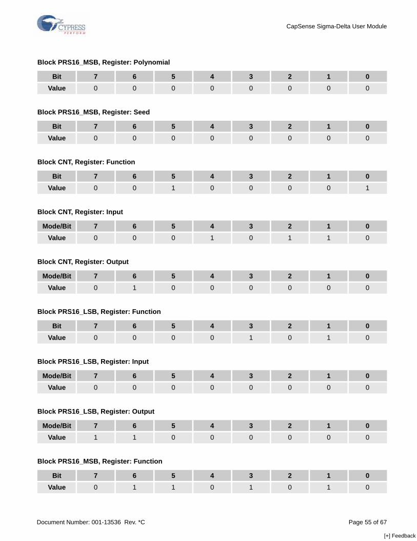
CapSense Sigma-Delta User Module
Document Number: 001-13536 Rev. *C Page 55 of 67
Block PRS16_MSB, Register: Polynomial
Bit 7 6 5 4 3 2 1 0Value 0 0 0 0 0 0 0 0
Block PRS16_MSB, Register: Seed
Bit 7 6 5 4 3 2 1 0Value 0 0 0 0 0 0 0 0
Block CNT, Register: Function
Bit 7 6 5 4 3 2 1 0Value 0 0 1 0 0 0 0 1
Block CNT, Register: Input
Mode/Bit 7 6 5 4 3 2 1 0Value 0 0 0 1 0 1 1 0
Block CNT, Register: Output
Mode/Bit 7 6 5 4 3 2 1 0Value 0 1 0 0 0 0 0 0
Block PRS16_LSB, Register: Function
Bit 7 6 5 4 3 2 1 0Value 0 0 0 0 1 0 1 0
Block PRS16_LSB, Register: Input
Mode/Bit 7 6 5 4 3 2 1 0Value 0 0 0 0 0 0 0 0
Block PRS16_LSB, Register: Output
Mode/Bit 7 6 5 4 3 2 1 0Value 1 1 0 0 0 0 0 0
Block PRS16_MSB, Register: Function
Bit 7 6 5 4 3 2 1 0Value 0 1 1 0 1 0 1 0
[+] Feedback
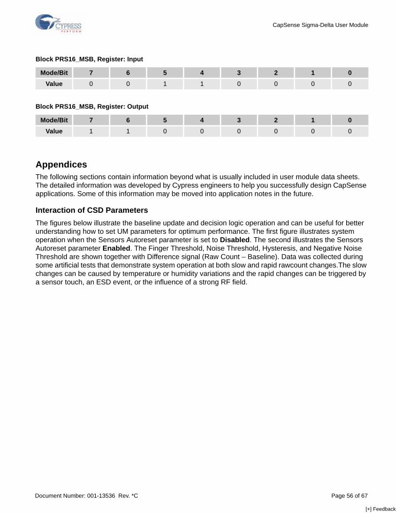
CapSense Sigma-Delta User Module
Document Number: 001-13536 Rev. *C Page 56 of 67
AppendicesThe following sections contain information beyond what is usually included in user module data sheets. The detailed information was developed by Cypress engineers to help you successfully design CapSense applications. Some of this information may be moved into application notes in the future.
Interaction of CSD ParametersThe figures below illustrate the baseline update and decision logic operation and can be useful for better understanding how to set UM parameters for optimum performance. The first figure illustrates system operation when the Sensors Autoreset parameter is set to Disabled. The second illustrates the Sensors Autoreset parameter Enabled. The Finger Threshold, Noise Threshold, Hysteresis, and Negative Noise Threshold are shown together with Difference signal (Raw Count – Baseline). Data was collected during some artificial tests that demonstrate system operation at both slow and rapid rawcount changes.The slow changes can be caused by temperature or humidity variations and the rapid changes can be triggered by a sensor touch, an ESD event, or the influence of a strong RF field.
Block PRS16_MSB, Register: Input
Mode/Bit 7 6 5 4 3 2 1 0Value 0 0 1 1 0 0 0 0
Block PRS16_MSB, Register: Output
Mode/Bit 7 6 5 4 3 2 1 0Value 1 1 0 0 0 0 0 0
[+] Feedback
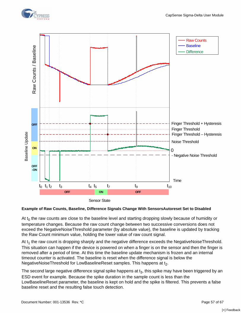
CapSense Sigma-Delta User Module
Document Number: 001-13536 Rev. *C Page 57 of 67
Example of Raw Counts, Baseline, Difference Signals Change With SensorsAutoreset Set to Disabled
At t0 the raw counts are close to the baseline level and starting dropping slowly because of humidity or temperature changes. Because the raw count change between two successive conversions does not exceed the NegativeNoiseThreshold parameter (by absolute value), the baseline is updated by tracking the Raw Count minimum value, holding the lower value of raw count signal.At t1 the raw count is dropping sharply and the negative difference exceeds the NegativeNoiseThreshold. This situation can happen if the device is powered on when a finger is on the sensor and then the finger is removed after a period of time. At this time the baseline update mechanism is frozen and an internal timeout counter is activated. The baseline is reset when the difference signal is below the NegativeNoiseThreshold for LowBaselineReset samples. This happens at t2.
The second large negative difference signal spike happens at t3, this spike may have been triggered by an ESD event for example. Because the spike duration in the sample count is less than the LowBaselineReset parameter, the baseline is kept on hold and the spike is filtered. This prevents a false baseline reset and the resulting false touch detection.
Raw CountsBaselineDifference
Noise Threshold
Finger ThresholdFinger Threshold + Hysteresis
Finger Threshold – Hysteresis
- Negative Noise Threshold
OFF-ON
ON
OFF
Time
Bas
elin
e U
pdat
e
t1 t2 t3 t4 t5 t7 t9t0 t10
Sensor State
OFF ON OFF
0
Raw
Cou
nts
/ Bas
elin
e
[+] Feedback
CapSense Sigma-Delta User Module
Document Number: 001-13536 Rev. *C Page 58 of 67
The sensor is touched at t4. When the difference signal exceeds the FingerThreshold + Hysteresis value, the internal debounce counter is activated. If the signal exceeds this value for more than Debounce samples, the sensor state is set to on. This happens at t5. The sensor state reverts back to the off state immediately when the difference signal drops below the FingerThreshold – Hysteresis level at t7. The short positive spike at t9 is filtered by the debounce counter because the spike duration in sample units does not exceed the Debounce value.The raw count drifts up slowly between t7 and t10. The baseline is updated using the bucket algorithm when the difference signal is below the NoiseThreshold (SensorsAutoreset is set to Disabled), the difference signal is proportional to the drift rate. It is possible to control the baseline update speed using the BaselineUpdate Threshold parameter. Lower parameter values provide faster baseline update speeds.
Example of Raw Counts, Baseline, Difference Signals Change With SensorsAutoreset Set to Enabled
The system operation in the above figure is similar to the operation in the previous case, except for the following differences:
Raw CountsBaselineDifference
Noise Threshold
Finger ThresholdFinger Threshold + Hysteresis
- Negative Noise Threshold
OFF-ON
ON
Time
Bas
elin
e U
pdat
e
t5
Sensor State
OFF ON OFF
0
Raw
Cou
nts
/ Bas
elin
e
t1 t2 t3 t4 t6 t9t0 t10t7 t8
Finger Threshold - Hysteresis
[+] Feedback
CapSense Sigma-Delta User Module
Document Number: 001-13536 Rev. *C Page 59 of 67
• The touch duration is decreased because of the active baseline update algorithm while the sensor is touched, t6.
• After the finger is removed, the baseline is reset after LowBaselineReset samples (t8), which blocks touch detetion for a short time. This serves as an additional debouce mechanism.
CSD Step-By-Step Tuning GuideThe success of capacitive sensing depends on setting the parameters optimally for the given sensing electrodes. Variables that will affect these settings include:
• Geometric dimensions of the electrodes• Overlay thickness and dielectric constant• Electrode connection resistance to the PSoC device• The end application conditions such as
• Presence of a power supply • Temperature• Humidity• Presence of moisture• ESD, EMC, or EMI requirements
The best practices for different tasks (waterproof operation, sensing using high-resistance materials, proximity detection, and operation via thick overlays and recommendations for passing certification tests) are described in separate application notes. Here are basic guidelines for configuring the user module in a typical CapSense application using the CY3214 board as a test example. The sense zone is covered with a 2 mm plastic overlay. Configure the CSD User Module parameters in the following steps:1. Prepare the target board. Assemble the target application PCB and fix the overlay on it. Use glue or
special adhesive tape for this purpose. Avoid air gaps between the PCB and the overlay as it can reduce sensitivity substantially and cause multiple false button triggers because of the arguable shift-ing under your touch.
2. Set up a real-time monitoring tool to monitor data. During CSD configuration use a PC charting tool that allows you to observe one or more data series in real time. The raw count, baseline, and signal differ-ences must be observed during the user module tuning procedures. You can use an I2C-USB bridge for this. One was used to monitor raw count data during our tests. Another good alternative is to use the USBUART User Module to send debug information via an emulated serial port.
Please do not use the LCD or any other numerical displays to monitor counts because they are slow and do not allow you to visualize the data dynamics.
[+] Feedback
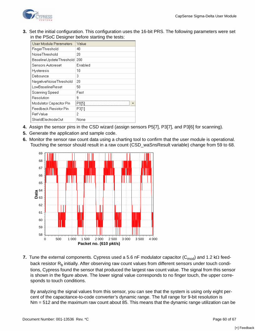
CapSense Sigma-Delta User Module
Document Number: 001-13536 Rev. *C Page 60 of 67
3. Set the initial configuration. This configuration uses the 16-bit PRS. The following parameters were set in the PSoC Designer before starting the tests:
4. Assign the sensor pins in the CSD wizard (assign sensors P5[7], P3[7], and P3[6] for scanning). 5. Generate the application and sample code. 6. Monitor the sensor raw count data using a charting tool to confirm that the user module is operational.
Touching the sensor should result in a raw count (CSD_waSnsResult variable) change from 59 to 68.
7. Tune the external components. Cypress used a 5.6 nF modulator capacitor (Cmod) and 1.2 kΩ feed-back resistor Rb initially. After observing raw count values from different sensors under touch condi-tions, Cypress found the sensor that produced the largest raw count value. The signal from this sensor is shown in the figure above. The lower signal value corresponds to no finger touch, the upper corre-sponds to touch conditions.
By analyzing the signal values from this sensor, you can see that the system is using only eight per-cent of the capacitance-to-code converter’s dynamic range. The full range for 9-bit resolution is Nm = 512 and the maximum raw count about 85. This means that the dynamic range utilization can be
Packet no. (610 pkt/s)4 0003 5003 0002 5002 0001 5001 0005000
Dat
a
69
68
67
66
65
64
63
62
61
60
59
58
[+] Feedback
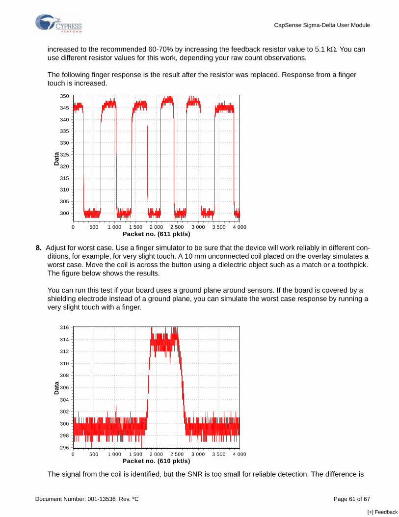
CapSense Sigma-Delta User Module
Document Number: 001-13536 Rev. *C Page 61 of 67
increased to the recommended 60-70% by increasing the feedback resistor value to 5.1 kΩ. You can use different resistor values for this work, depending your raw count observations.
The following finger response is the result after the resistor was replaced. Response from a finger touch is increased.
8. Adjust for worst case. Use a finger simulator to be sure that the device will work reliably in different con-ditions, for example, for very slight touch. A 10 mm unconnected coil placed on the overlay simulates a worst case. Move the coil is across the button using a dielectric object such as a match or a toothpick. The figure below shows the results.
You can run this test if your board uses a ground plane around sensors. If the board is covered by a shielding electrode instead of a ground plane, you can simulate the worst case response by running a very slight touch with a finger.
The signal from the coil is identified, but the SNR is too small for reliable detection. The difference is
Packet no. (611 pkt/s)4 0003 5003 0002 5002 0001 5001 0005000
Dat
a
350
345
340
335
330
325
320
315
310
305
300
Packet no. (610 pkt/s)4 0003 5003 0002 5002 0001 5001 0005000
Dat
a
316
314
312
310
308
306
304
302
300
298
296
[+] Feedback
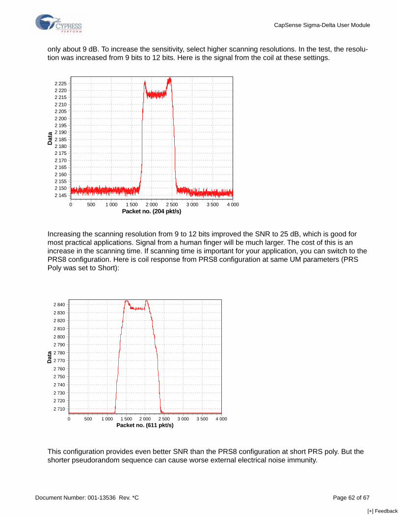
CapSense Sigma-Delta User Module
Document Number: 001-13536 Rev. *C Page 62 of 67
only about 9 dB. To increase the sensitivity, select higher scanning resolutions. In the test, the resolu-tion was increased from 9 bits to 12 bits. Here is the signal from the coil at these settings.
Increasing the scanning resolution from 9 to 12 bits improved the SNR to 25 dB, which is good for most practical applications. Signal from a human finger will be much larger. The cost of this is an increase in the scanning time. If scanning time is important for your application, you can switch to the PRS8 configuration. Here is coil response from PRS8 configuration at same UM parameters (PRS Poly was set to Short):
This configuration provides even better SNR than the PRS8 configuration at short PRS poly. But the shorter pseudorandom sequence can cause worse external electrical noise immunity.
Packet no. (204 pkt/s)4 0003 5003 0002 5002 0001 5001 0005000
Dat
a
2 2252 2202 2152 2102 2052 2002 1952 1902 1852 1802 1752 1702 1652 1602 1552 1502 145
Packet no. (611 pkt/s)4 0003 5003 0002 5002 0001 5001 0005000
Dat
a
2 840
2 830
2 820
2 810
2 800
2 790
2 780
2 770
2 760
2 750
2 740
2 730
2 720
2 710
[+] Feedback
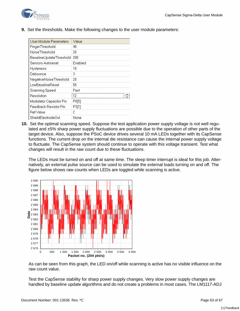
CapSense Sigma-Delta User Module
Document Number: 001-13536 Rev. *C Page 63 of 67
9. Set the thresholds. Make the following changes to the user module parameters:
10. Set the optimal scanning speed. Suppose the test application power supply voltage is not well regu-lated and ±5% sharp power supply fluctuations are possible due to the operation of other parts of the target device. Also, suppose the PSoC device drives several 10 mA LEDs together with its CapSense functions. The current drop on the internal die resistance can cause the internal power supply voltage to fluctuate. The CapSense system should continue to operate with this voltage transient. Test what changes will result in the raw count due to these fluctuations.
The LEDs must be turned on and off at same time. The sleep timer interrupt is ideal for this job. Alter-natively, an external pulse source can be used to simulate the external loads turning on and off. The figure below shows raw counts when LEDs are toggled while scanning is active.
As can be seen from this graph, the LED on/off while scanning is active has no visible influence on the raw count value.
Test the CapSense stability for sharp power supply changes. Very slow power supply changes are handled by baseline update algorithms and do not create a problems in most cases. The LM1117-ADJ
Packet no. (204 pkt/s)4 0003 5003 0002 5002 0001 5001 0005000
Dat
a
2 690
2 689
2 688
2 687
2 686
2 685
2 684
2 683
2 682
2 681
2 680
2 679
2 678
2 677
2 676
[+] Feedback
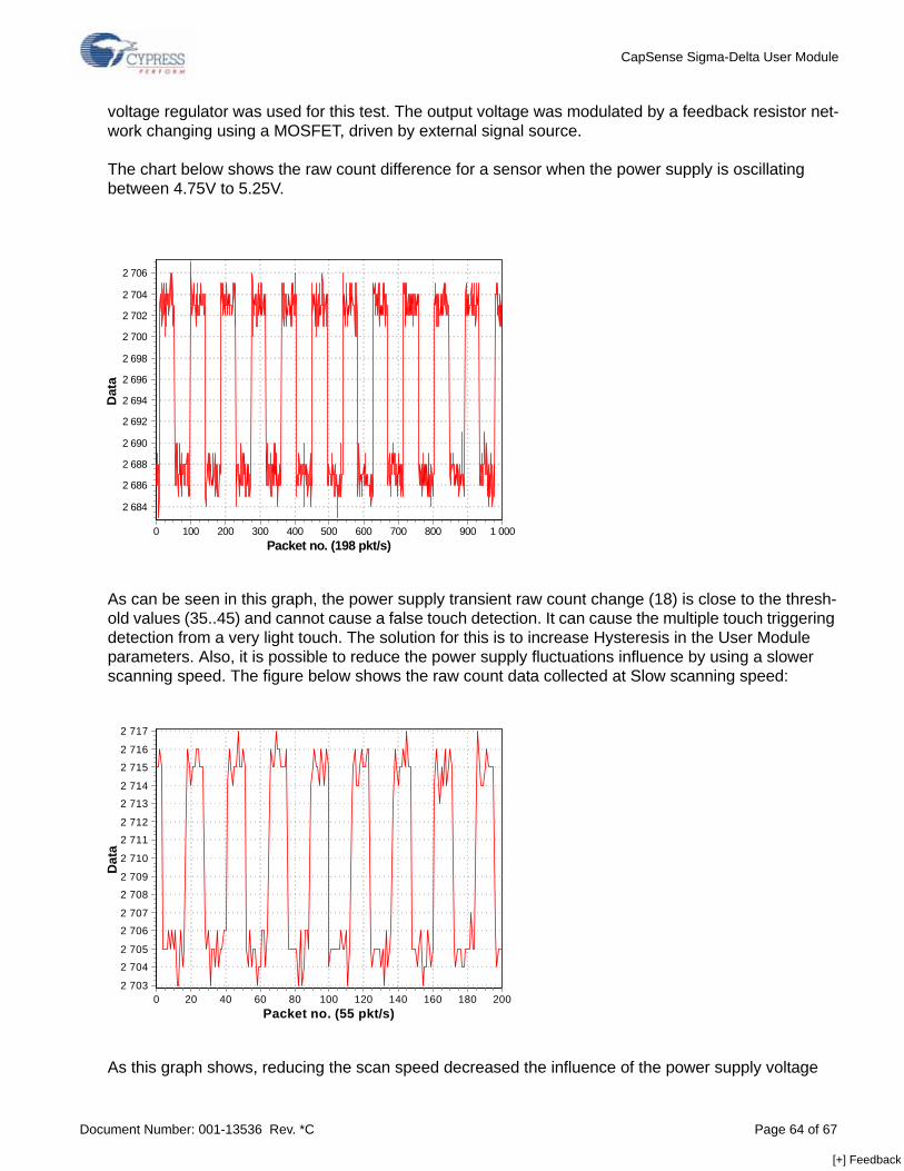
CapSense Sigma-Delta User Module
Document Number: 001-13536 Rev. *C Page 64 of 67
voltage regulator was used for this test. The output voltage was modulated by a feedback resistor net-work changing using a MOSFET, driven by external signal source.
The chart below shows the raw count difference for a sensor when the power supply is oscillating between 4.75V to 5.25V.
As can be seen in this graph, the power supply transient raw count change (18) is close to the thresh-old values (35..45) and cannot cause a false touch detection. It can cause the multiple touch triggering detection from a very light touch. The solution for this is to increase Hysteresis in the User Module parameters. Also, it is possible to reduce the power supply fluctuations influence by using a slower scanning speed. The figure below shows the raw count data collected at Slow scanning speed:
As this graph shows, reducing the scan speed decreased the influence of the power supply voltage
Packet no. (198 pkt/s)1 0009008007006005004003002001000
Dat
a
2 706
2 704
2 702
2 700
2 698
2 696
2 694
2 692
2 690
2 688
2 686
2 684
Packet no. (55 pkt/s)200180160140120100806040200
Dat
a
2 717
2 716
2 715
2 714
2 713
2 712
2 711
2 710
2 709
2 708
2 707
2 706
2 705
2 704
2 703
[+] Feedback
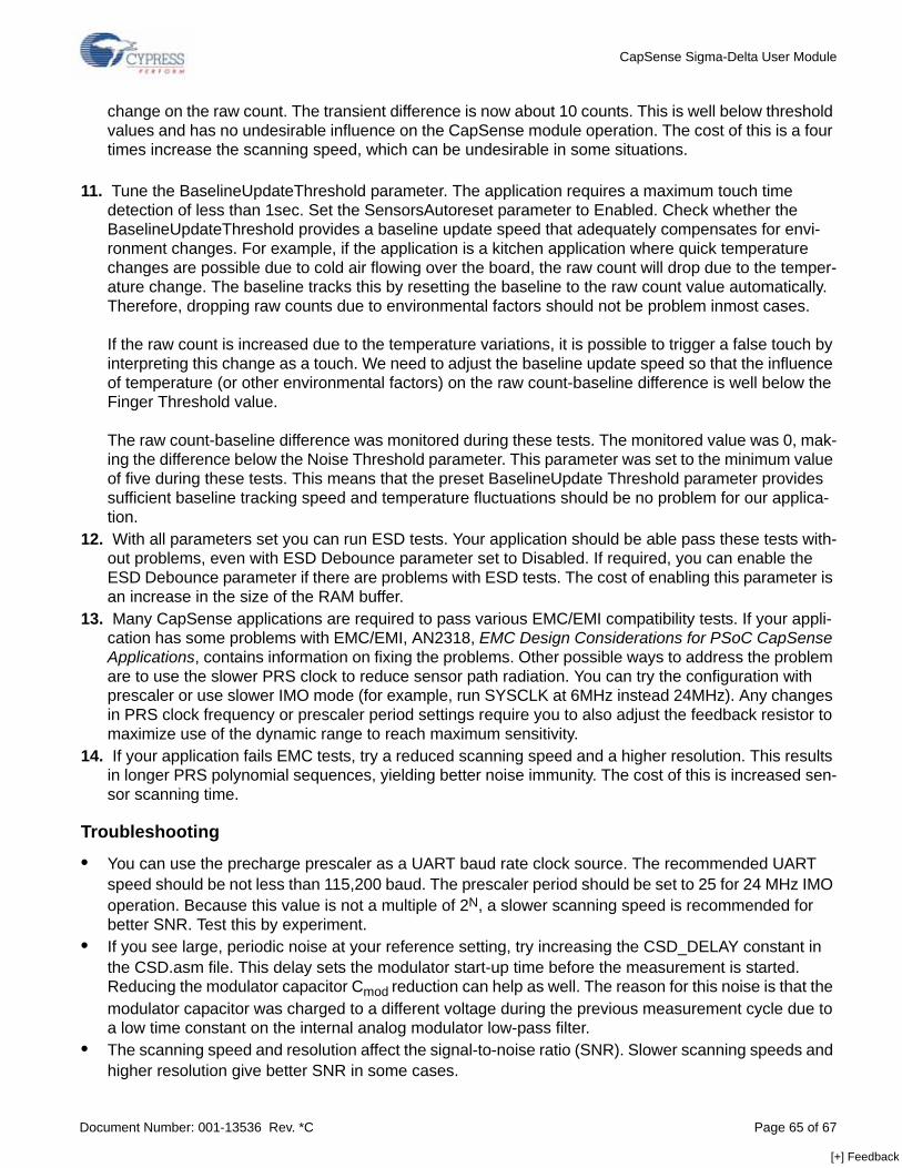
CapSense Sigma-Delta User Module
Document Number: 001-13536 Rev. *C Page 65 of 67
change on the raw count. The transient difference is now about 10 counts. This is well below threshold values and has no undesirable influence on the CapSense module operation. The cost of this is a four times increase the scanning speed, which can be undesirable in some situations.
11. Tune the BaselineUpdateThreshold parameter. The application requires a maximum touch time detection of less than 1sec. Set the SensorsAutoreset parameter to Enabled. Check whether the BaselineUpdateThreshold provides a baseline update speed that adequately compensates for envi-ronment changes. For example, if the application is a kitchen application where quick temperature changes are possible due to cold air flowing over the board, the raw count will drop due to the temper-ature change. The baseline tracks this by resetting the baseline to the raw count value automatically. Therefore, dropping raw counts due to environmental factors should not be problem inmost cases.
If the raw count is increased due to the temperature variations, it is possible to trigger a false touch by interpreting this change as a touch. We need to adjust the baseline update speed so that the influence of temperature (or other environmental factors) on the raw count-baseline difference is well below the Finger Threshold value.
The raw count-baseline difference was monitored during these tests. The monitored value was 0, mak-ing the difference below the Noise Threshold parameter. This parameter was set to the minimum value of five during these tests. This means that the preset BaselineUpdate Threshold parameter provides sufficient baseline tracking speed and temperature fluctuations should be no problem for our applica-tion.
12. With all parameters set you can run ESD tests. Your application should be able pass these tests with-out problems, even with ESD Debounce parameter set to Disabled. If required, you can enable the ESD Debounce parameter if there are problems with ESD tests. The cost of enabling this parameter is an increase in the size of the RAM buffer.
13. Many CapSense applications are required to pass various EMC/EMI compatibility tests. If your appli-cation has some problems with EMC/EMI, AN2318, EMC Design Considerations for PSoC CapSense Applications, contains information on fixing the problems. Other possible ways to address the problem are to use the slower PRS clock to reduce sensor path radiation. You can try the configuration with prescaler or use slower IMO mode (for example, run SYSCLK at 6MHz instead 24MHz). Any changes in PRS clock frequency or prescaler period settings require you to also adjust the feedback resistor to maximize use of the dynamic range to reach maximum sensitivity.
14. If your application fails EMC tests, try a reduced scanning speed and a higher resolution. This results in longer PRS polynomial sequences, yielding better noise immunity. The cost of this is increased sen-sor scanning time.
Troubleshooting
• You can use the precharge prescaler as a UART baud rate clock source. The recommended UART speed should be not less than 115,200 baud. The prescaler period should be set to 25 for 24 MHz IMO operation. Because this value is not a multiple of 2N, a slower scanning speed is recommended for better SNR. Test this by experiment.
• If you see large, periodic noise at your reference setting, try increasing the CSD_DELAY constant in the CSD.asm file. This delay sets the modulator start-up time before the measurement is started. Reducing the modulator capacitor Cmod reduction can help as well. The reason for this noise is that the modulator capacitor was charged to a different voltage during the previous measurement cycle due to a low time constant on the internal analog modulator low-pass filter.
• The scanning speed and resolution affect the signal-to-noise ratio (SNR). Slower scanning speeds and higher resolution give better SNR in some cases.
[+] Feedback
CapSense Sigma-Delta User Module
Document Number: 001-13536 Rev. *C Page 66 of 67
• When the electrode overlay is thick, higher resolution and slower scanning speed may be required.• The PRS polynomial is automatically adjusted depending on the scanning speed and resolution so
that the PRS sequence repeat period is close to the sample conversion cycle count. Slower scanning rates and higher resolutions provide better noise immunity during EMC tests because it produces longer PRS sequences.
• Slower scanning speeds results in lower modulator operation frequency, making readings less depen-dent on the comparator dynamic characteristics. When you need good raw count stability despite power supply fluctuations or when the PSoC device controls high-current loads, use the analog modu-lator to form the comparator reference internally. The recommended scanning speed in this situation is Normal or Slow.
• The Sigma-Delta conversion method belongs to the class of integrating methods. It demonstrates the best performance at higher resolutions. Use the longest scanning time possible. Use 1 ms for sensor scanning for best results.
• The shield elecrode can be used effectively to reduce the stray capacitance influence even in applica-tions that do not need to be water resistant. In this case the shield electrode can be located on the bot-tom layer of the PCB under the capacitive sensor zone. A hatch filling pattern is recommended in this case to decrease the capacitance of the shielding electrode.
Use Warnings
Eliminate Possible Resource Use Conflicts Be careful not to alter the hardware configurations used by this user module. This includes:
• The GlobalOutEven_1 or GlobalOutEven_5 (depending on your modulator feedback resistor pin selec-tion) buses are used internally to pass comparator output signal to the output bus. Do not connect any sources to these buses.
• Do not change the Comparator Bus 1 LUT functions. The Comparator Bus_1 should be set to ~A.• The analog column one clock source should be set to VC1.• The VC1 are set internally by the user module. The value entered in the Global Resources are over-
written at runtime.• When using a shield electrode, please set the row LUT function to A.
Interrupt Duration ManagementManage your Interrupt Service Routine (ISR) duration when sensor scanning is active for the PRS16 configuration. The 8-bit timer is clocked from VC2. The worse-case overflow interval for timer is:
Equation 25
FIMO – IMO frequency, VC1 = 2, 4,or 8 for Fast, Normal, or Slow scanning speeds respectively
VC2 – This value is set to four at all times.
This interval does not cause problems in the most cases. In some cases it needs to be checked.
ISSP Pins Possible Conflicts Permanent connection of a low-resistance feedback resistor to the P1[1] pin can cause ISSP programming faults. Use another pin for this.
Towf VC2 VC1256
FIMO--------------⋅=
[+] Feedback
CapSense Sigma-Delta User Module
Document Number: 001-13536 Rev. *C Revised February 12, 2009 Page 67 of 67© Cypress Semiconductor Corporation, 2007-2009. The information contained herein is subject to change without notice. Cypress Semiconductor Corporation assumes no responsibility for theuse of any circuitry other than circuitry embodied in a Cypress product. Nor does it convey or imply any license under patent or other rights. Cypress products are not warranted nor intended to beused for medical, life support, life saving, critical control or safety applications, unless pursuant to an express written agreement with Cypress. Furthermore, Cypress does not authorize its productsfor use as critical components in life-support systems where a malfunction or failure may reasonably be expected to result in significant injury to the user. The inclusion of Cypress products in life-support systems application implies that the manufacturer assumes all risk of such use and in doing so indemnifies Cypress against all charges.
PSoC Designer™, Programmable System-on-Chip™, and PSoC Express™ are trademarks and PSoC® is a registered trademark of Cypress Semiconductor Corp. All other trademarks or registeredtrademarks referenced herein are property of the respective corporations.
Any Source Code (software and/or firmware) is owned by Cypress Semiconductor Corporation (Cypress) and is protected by and subject to worldwide patent protection (United States and foreign),United States copyright laws and international treaty provisions. Cypress hereby grants to licensee a personal, non-exclusive, non-transferable license to copy, use, modify, create derivative worksof, and compile the Cypress Source Code and derivative works for the sole purpose of creating custom software and or firmware in support of licensee product to be used only in conjunction witha Cypress integrated circuit as specified in the applicable agreement. Any reproduction, modification, translation, compilation, or representation of this Source Code except as specified above isprohibited without the express written permission of Cypress.
Disclaimer: CYPRESS MAKES NO WARRANTY OF ANY KIND, EXPRESS OR IMPLIED, WITH REGARD TO THIS MATERIAL, INCLUDING, BUT NOT LIMITED TO, THE IMPLIED WARRANTIESOF MERCHANTABILITY AND FITNESS FOR A PARTICULAR PURPOSE. Cypress reserves the right to make changes without further notice to the materials described herein. Cypress does notassume any liability arising out of the application or use of any product or circuit described herein. Cypress does not authorize its products for use as critical components in life-support systemswhere a malfunction or failure may reasonably be expected to result in significant injury to the user. The inclusion of Cypress' product in a life-support systems application implies that the manufacturerassumes all risk of such use and in doing so indemnifies Cypress against all charges.
Use may be limited by and subject to the applicable Cypress software license agreement.
Clock SpeedThe CPU speed for CY8C24x94 devices should be SysClk/32 or faster for proper functionality..
[+] Feedback