1. d & e frame.pdf
TRANSCRIPT

7/16/2019 1. D & E Frame.pdf
http://slidepdf.com/reader/full/1-d-e-framepdf 1/197
Contents
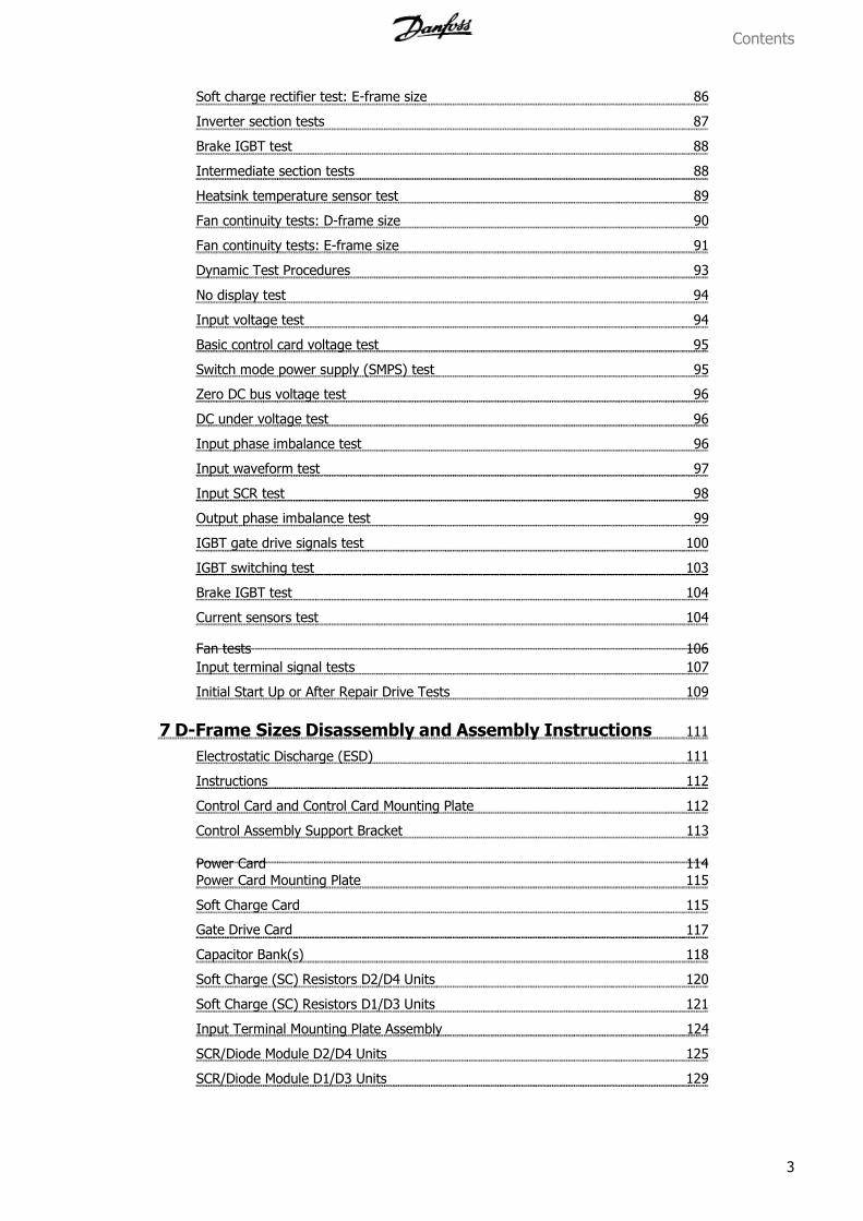
1 Introduction 11
Purpose 11
VLT FC Product Overview 11
For Your Safety 11Electrostatic Discharge (ESD) 12
Frame Size Definitions 12
Tools Required 14
General Torque Tightening Values 14
Exploded Views 15
Ratings Tables 19
2 Operator Interface and Drive Control 25
Introduction 25User Interface 25
Numeric Local Control Panel (NLCP) 30
Tips and tricks 30
Status Messages 30
Status Messages 30
Service Functions 33
Drive Inputs and Outputs 35
Input signals 35
Output signals 36
Control Terminals 36
Control Terminal Functions 38
Grounding Shielded Cables 40
3 Internal Drive Operation 41
General 41
Description of Operation 41
Logic section 41
Logic to power interface 43
Power section 44
Sequence of Operation 45
Rectifier section 45
Intermediate section 47
Inverter section 49
Brake option 51
Cooling fans 53
Fan speed control 53
Load Sharing 54
Contents
1

7/16/2019 1. D & E Frame.pdf
http://slidepdf.com/reader/full/1-d-e-framepdf 2/197
Specific card connections 54
4 Troubleshooting 55
Troubleshooting Tips 55
Exterior Fault Troubleshooting 55
Fault Symptom Troubleshooting 55 Visual Inspection 55
Fault Symptoms 57
No display 57
Intermittent display 57
Motor will not run 57
Incorrect motor operation 58
Warning/Alarm Messages 59
Warning/alarm code list 59
After Repair Tests 67
5 Drive and Motor Applications 69
Torque Limit, Current Limit, and Unstable Motor Operation 69
Overvoltage trips 69
Mains phase loss trips 70
Control logic problems 70
Programming problems 71
Motor/load problems 71
Internal Drive Problems 71
Overtemperature faults 71
Current sensor faults 72
Signal and power wiring considerations for drive electromagnetic compatibility 72
Effect of EMI 72
Sources of EMI 73
EMI propagation 73
Preventive measures 74
Proper EMC installation 75
6 Test Procedures 77
Introduction 77
Tools required for testing 77
Signal test board 78
Test cables 78
Static Test Procedures 79
Soft charge and rectifier circuits test: D-frame size 80
Soft charge rectifier test: D-frame size 81
Soft charge and rectifier circuits test: E-frame sizes 84
Contents
2
7/16/2019 1. D & E Frame.pdf
http://slidepdf.com/reader/full/1-d-e-framepdf 3/197
Soft charge rectifier test: E-frame size 86
Inverter section tests 87
Brake IGBT test 88
Intermediate section tests 88
Heatsink temperature sensor test 89
Fan continuity tests: D-frame size 90
Fan continuity tests: E-frame size 91
Dynamic Test Procedures 93
No display test 94
Input voltage test 94
Basic control card voltage test 95
Switch mode power supply (SMPS) test 95
Zero DC bus voltage test 96
DC under voltage test 96
Input phase imbalance test 96
Input waveform test 97
Input SCR test 98
Output phase imbalance test 99
IGBT gate drive signals test 100
IGBT switching test 103
Brake IGBT test 104
Current sensors test 104
Fan tests 106
Input terminal signal tests 107
Initial Start Up or After Repair Drive Tests 109
7 D-Frame Sizes Disassembly and Assembly Instructions 111
Electrostatic Discharge (ESD) 111
Instructions 112
Control Card and Control Card Mounting Plate 112
Control Assembly Support Bracket 113
Power Card 114
Power Card Mounting Plate 115
Soft Charge Card 115
Gate Drive Card 117
Capacitor Bank(s) 118
Soft Charge (SC) Resistors D2/D4 Units 120
Soft Charge (SC) Resistors D1/D3 Units 121
Input Terminal Mounting Plate Assembly 124
SCR/Diode Module D2/D4 Units 125
SCR/Diode Module D1/D3 Units 129
Contents
3

7/16/2019 1. D & E Frame.pdf
http://slidepdf.com/reader/full/1-d-e-framepdf 4/197
Current Sensor 133
Heatsink Fan Assembly 134
AC Input Terminals 136
IGBT Modules D2/D4 Units 137
IGBT modules D1/D3 units 140
8 E-Frame Sizes Disassembly and Assembly Instructions 143
Electrostatic Discharge (ESD) 143
Instructions 144
Control Card and Control Card Mounting Plate 144
Control Assembly Support Bracket 145
Power Card 146
Soft Charge Card 147
Gate Drive Card 148
Capacitor Banks 149
Input Terminal Mounting Plate Assy Option 151
Soft Charge Resistor 152
SCR and Diode Modules 153
Current Sensor 156
Heatsink Fan Assembly 157
AC Input, Motor, Load Sharing or Regen Terminals 158
IGBT Modules 159
9 Special Test Equipment 165
Test Equipment 165
Test cables and SCR shorting plug kit p/n 176F8439 165
Signal test board (p/n 176F8437) 166
Signal test board pin outs: Description and voltage levels 166
10 Spare Parts List 169
Spare Parts List 169
General Notes 169
Spare Parts Lists 170
11 Block Diagrams 191
Block Diagrams for D-Frames 191
D1/D3 380 - 500 VAC 191
D2/D4 380 - 500 VAC 192
D1/D3 525 - 690 VAC 193
D2/D4 525 - 690 VAC 194
Block Diagrams for E-Frames 194
E 380 - 500 VAC 195
Contents
4

7/16/2019 1. D & E Frame.pdf
http://slidepdf.com/reader/full/1-d-e-framepdf 5/197
E 525 - 690 VAC 196
Index 197
Contents
5
7/16/2019 1. D & E Frame.pdf
http://slidepdf.com/reader/full/1-d-e-framepdf 6/197
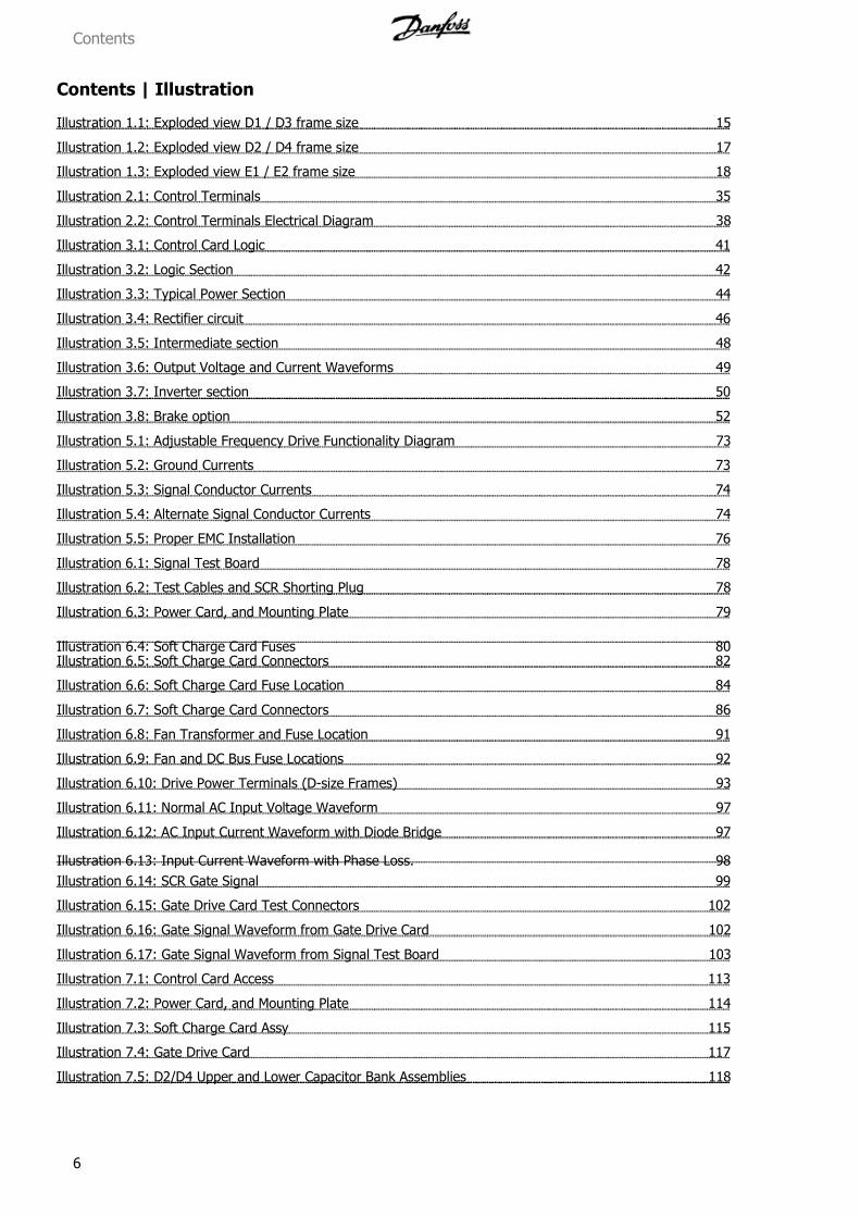
Contents | Illustration
Illustration 1.1: Exploded view D1 / D3 frame size 15
Illustration 1.2: Exploded view D2 / D4 frame size 17
Illustration 1.3: Exploded view E1 / E2 frame size 18
Illustration 2.1: Control Terminals 35
Illustration 2.2: Control Terminals Electrical Diagram 38
Illustration 3.1: Control Card Logic 41
Illustration 3.2: Logic Section 42
Illustration 3.3: Typical Power Section 44
Illustration 3.4: Rectifier circuit 46
Illustration 3.5: Intermediate section 48
Illustration 3.6: Output Voltage and Current Waveforms 49
Illustration 3.7: Inverter section 50
Illustration 3.8: Brake option 52
Illustration 5.1: Adjustable Frequency Drive Functionality Diagram 73
Illustration 5.2: Ground Currents 73
Illustration 5.3: Signal Conductor Currents 74
Illustration 5.4: Alternate Signal Conductor Currents 74
Illustration 5.5: Proper EMC Installation 76
Illustration 6.1: Signal Test Board 78
Illustration 6.2: Test Cables and SCR Shorting Plug 78
Illustration 6.3: Power Card, and Mounting Plate 79
Illustration 6.4: Soft Charge Card Fuses 80Illustration 6.5: Soft Charge Card Connectors 82
Illustration 6.6: Soft Charge Card Fuse Location 84
Illustration 6.7: Soft Charge Card Connectors 86
Illustration 6.8: Fan Transformer and Fuse Location 91
Illustration 6.9: Fan and DC Bus Fuse Locations 92
Illustration 6.10: Drive Power Terminals (D-size Frames) 93
Illustration 6.11: Normal AC Input Voltage Waveform 97
Illustration 6.12: AC Input Current Waveform with Diode Bridge 97
Illustration 6.13: Input Current Waveform with Phase Loss. 98
Illustration 6.14: SCR Gate Signal 99
Illustration 6.15: Gate Drive Card Test Connectors 102
Illustration 6.16: Gate Signal Waveform from Gate Drive Card 102
Illustration 6.17: Gate Signal Waveform from Signal Test Board 103
Illustration 7.1: Control Card Access 113
Illustration 7.2: Power Card, and Mounting Plate 114
Illustration 7.3: Soft Charge Card Assy 115
Illustration 7.4: Gate Drive Card 117
Illustration 7.5: D2/D4 Upper and Lower Capacitor Bank Assemblies 118
Contents
6
7/16/2019 1. D & E Frame.pdf
http://slidepdf.com/reader/full/1-d-e-framepdf 7/197
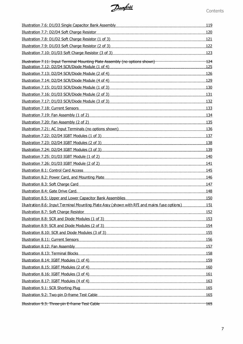
Illustration 7.6: D1/D3 Single Capacitor Bank Assembly 119
Illustration 7.7: D2/D4 Soft Charge Resistor 120
Illustration 7.8: D1/D2 Soft Charge Resistor (1 of 3) 121
Illustration 7.9: D1/D3 Soft Charge Resistor (2 of 3) 122
Illustration 7.10: D1/D3 Soft Charge Resistor (3 of 3) 123
Illustration 7.11: Input Terminal Mounting Plate Assembly (no options shown) 124
Illustration 7.12: D2/D4 SCR/Diode Module (1 of 4) 125
Illustration 7.13: D2/D4 SCR/Diode Module (2 of 4) 126
Illustration 7.14: D2/D4 SCR/Diode Module (4 of 4) 129
Illustration 7.15: D1/D3 SCR/Diode Module (1 of 3) 130
Illustration 7.16: D1/D3 SCR/Diode Module (2 of 3) 131
Illustration 7.17: D1/D3 SCR/Diode Module (3 of 3) 132
Illustration 7.18: Current Sensors 133
Illustration 7.19: Fan Assembly (1 of 2) 134
Illustration 7.20: Fan Assembly (2 of 2) 135
Illustration 7.21: AC Input Terminals (no options shown) 136
Illustration 7.22: D2/D4 IGBT Modules (1 of 3) 137
Illustration 7.23: D2/D4 IGBT Modules (2 of 3) 138
Illustration 7.24: D2/D4 IGBT Modules (3 of 3) 139
Illustration 7.25: D1/D3 IGBT Module (1 of 2) 140
Illustration 7.26: D1/D3 IGBT Module (2 of 2) 141
Illustration 8.1: Control Card Access 145
Illustration 8.2: Power Card, and Mounting Plate 146
Illustration 8.3: Soft Charge Card 147
Illustration 8.4: Gate Drive Card. 148
Illustration 8.5: Upper and Lower Capacitor Bank Assemblies 150
Illustration 8.6: Input Terminal Mounting Plate Assy (shown with RFI and mains fuse options) 151
Illustration 8.7: Soft Charge Resistor 152
Illustration 8.8: SCR and Diode Modules (1 of 3) 153
Illustration 8.9: SCR and Diode Modules (2 of 3) 154
Illustration 8.10: SCR and Diode Modules (3 of 3) 155
Illustration 8.11: Current Sensors 156
Illustration 8.12: Fan Assembly 157
Illustration 8.13: Terminal Blocks 158
Illustration 8.14: IGBT Modules (1 of 4) 159
Illustration 8.15: IGBT Modules (2 of 4) 160
Illustration 8.16: IGBT Modules (3 of 4) 161
Illustration 8.17: IGBT Modules (4 of 4) 163
Illustration 9.1: SCR Shorting Plug 165
Illustration 9.2: Two-pin D-frame Test Cable 165
Illustration 9.3: Three-pin E-frame Test Cable 165
Contents
7

7/16/2019 1. D & E Frame.pdf
http://slidepdf.com/reader/full/1-d-e-framepdf 8/197
Illustration 9.4: Signal Test Board 166
Contents
8
7/16/2019 1. D & E Frame.pdf
http://slidepdf.com/reader/full/1-d-e-framepdf 9/197
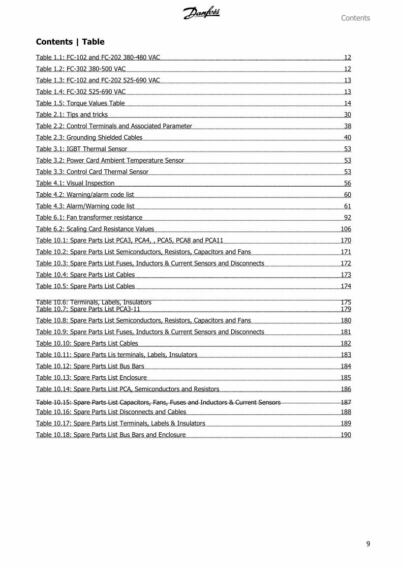
Contents | Table
Table 1.1: FC-102 and FC-202 380-480 VAC 12
Table 1.2: FC-302 380-500 VAC 12
Table 1.3: FC-102 and FC-202 525-690 VAC 13
Table 1.4: FC-302 525-690 VAC 13
Table 1.5: Torque Values Table 14
Table 2.1: Tips and tricks 30
Table 2.2: Control Terminals and Associated Parameter 38
Table 2.3: Grounding Shielded Cables 40
Table 3.1: IGBT Thermal Sensor 53
Table 3.2: Power Card Ambient Temperature Sensor 53
Table 3.3: Control Card Thermal Sensor 53
Table 4.1: Visual Inspection 56
Table 4.2: Warning/alarm code list 60
Table 4.3: Alarm/Warning code list 61
Table 6.1: Fan transformer resistance 92
Table 6.2: Scaling Card Resistance Values 106
Table 10.1: Spare Parts List PCA3, PCA4, , PCA5, PCA8 and PCA11 170
Table 10.2: Spare Parts List Semiconductors, Resistors, Capacitors and Fans 171
Table 10.3: Spare Parts List Fuses, Inductors & Current Sensors and Disconnects 172
Table 10.4: Spare Parts List Cables 173
Table 10.5: Spare Parts List Cables 174
Table 10.6: Terminals, Labels, Insulators 175Table 10.7: Spare Parts List PCA3-11 179
Table 10.8: Spare Parts List Semiconductors, Resistors, Capacitors and Fans 180
Table 10.9: Spare Parts List Fuses, Inductors & Current Sensors and Disconnects 181
Table 10.10: Spare Parts List Cables 182
Table 10.11: Spare Parts Lis terminals, Labels, Insulators 183
Table 10.12: Spare Parts List Bus Bars 184
Table 10.13: Spare Parts List Enclosure 185
Table 10.14: Spare Parts List PCA, Semiconductors and Resistors 186
Table 10.15: Spare Parts List Capacitors, Fans, Fuses and Inductors & Current Sensors 187
Table 10.16: Spare Parts List Disconnects and Cables 188
Table 10.17: Spare Parts List Terminals, Labels & Insulators 189
Table 10.18: Spare Parts List Bus Bars and Enclosure 190
Contents
9

7/16/2019 1. D & E Frame.pdf
http://slidepdf.com/reader/full/1-d-e-framepdf 10/197
1 Introduction
10
1

7/16/2019 1. D & E Frame.pdf
http://slidepdf.com/reader/full/1-d-e-framepdf 11/197
1 Introduction
1.1 Purpose
The purpose of this manual is to provide detailed technical information and instructions to enable a qualified technician to identify faults and perform
repairs on VLT FC series adjustable frequency drives of 125/150 hp to 650 hp.
It provides the reader with a general view of the unit's main assemblies and a description of the internal processing. With this information, technicians
should have a better understanding of the drive's operation to assist in troubleshooting and repair.
This manual provides instructions for the drive models and voltage ranges described in the tables on the following page.
1.2 VLT FC Product Overview
VLT HVAC FC 102 series drives are designed for the HVAC markets. They operate in variable torque mode or constant torque down to 15 Hz and include
special features and options well suited for fan and pump applications within the HVAC market.
VLT AQUA FC 202 series drives are designed for water and waste water markets. They can operate in either constant torque or variable torque with
limited overload capabilities. They include specific features and options which make them well suited for use on a variety of water pumping and processing
applications.
VLT AutomationDrive FC 302 series drives are fully programmable for either constant torque or variable torque industrial applications. They are full-
featured drives capable of operating a myriad of applications and incorporating a wide variety of control and communication options.
These models are available in Chassis/IP00, NEMA 1/IP21 or NEMA 12/IP54 enclosures.
1.3 For Your Safety
Drives contain dangerous voltages when connected to line voltage. Only a competent technician should carry out service.
For dynamic test procedures, main input power is required and all line powered devices and power supplies are energized at rated
voltage. Use extreme caution when conducting tests in a powered drive. Contact with powered components could result in electrical
shock and personal injury.
1 Introduction
11
1

7/16/2019 1. D & E Frame.pdf
http://slidepdf.com/reader/full/1-d-e-framepdf 12/197
1. DO NOT touch electrical parts of drive when AC line is connected. After AC line is disconnected wait 20 minutes before touching any components
in D-frame size units or 40 minutes for E-frame size units. See the label on the front of the drive door for specific discharge time.
2. When repair or inspection is made, AC line must be disconnected.
3. STOP key on control panel does not disconnect AC line.
4. During operation and while programming parameters, motor may start without warning. Activate STOP key when changing data.
When performing service, use proper ESD procedures to prevent damage to sensitive components.
1.4 Electrostatic Discharge (ESD)
Many electronic components within the adjustable frequency drive are sensitive to static electricity. Voltages so low that they cannot be felt, seen or
heard can reduce the life, affect performance, or completely destroy sensitive electronic components.
1.5 Frame Size Definitions
NB!
Frame size is used throughout this manual where ever procedures or components differ between drives based upon the unit's physical
size. Refer to these tables to determine frame size definitions.
380-480 VAC PowerModel FC-102 VLT HVAC Drive andFC-202 VLT AQUA Drive
kW @400 VAC HP @460 VAC Frame SizeP110 110 150 D1 / D3P132 132 200 D1 / D3P160 160 250 D2 / D4P200 200 300 D2 / D4P250 250 350 D2 / D4
P315 315 450 E1 / E2P355 355 500 E1 / E2P400 400 550 E1 / E2P450 450 600 E1 / E2
Table 1.1: FC-102 and FC-202 380-480 VAC
380-500 VAC PowerModel FC-302 VLT AutomationDrive High / Normal Overload
kW @400 VAC HP @460 VAC kW @500 VAC Frame SizeP90K 90 / 110 125 / 150 110 / 132 D1 / D3P110 110 / 132 150 / 200 132 / 160 D1 / D3P132 132 / 160 200 / 250 160 / 200 D2 / D4P160 160 / 200 250 / 300 200 / 250 D2 / D4
P200 200 / 250 300 / 350 250 / 315 D2 / D4P250 250 / 315 350 / 450 315 / 355 E1 / E2P315 315 / 355 450 / 500 355 / 400 E1 / E2P355 355 / 400 500 / 550 400 / 500 E1 / E2P400 400 / 450 550 / 600 500 / 530 E1 / E2
Table 1.2: FC-302 380-500 VAC
1 Introduction
12
1

7/16/2019 1. D & E Frame.pdf
http://slidepdf.com/reader/full/1-d-e-framepdf 13/197
525-690 VAC PowerModel FC-102 VLT HVAC Driveand FC-202 VLT AQUA Drive
kW @550 VAC HP @575 VAC kW @690 VAC Frame SizeP45K 37 50 45 D1 / D3P55K 45 60 55 D1 / D3P75K 55 75 75 D1 / D3P90K 75 100 90 D1 / D3P110 90 125 110 D1 / D3P132 110 150 132 D1 / D3P160 132 200 160 D1 / D3P200 160 250 200 D2 / D4P250 200 300 250 D2 / D4P315 250 350 315 D2 / D4P400 315 400 400 D2 / D4P450 355 450 450 E1 / E2P500 400 500 500 E1 / E2P560 450 600 560 E1 / E2P630 500 650 630 E1 / E2
Table 1.3: FC-102 and FC-202 525-690 VAC
525-690 VAC PowerModel FC-302 VLT AutomationDrive High / Normal Overload
kW @550 VAC HP @575 VAC kW @690 VAC Frame SizeP37k 30 / 37 40 / 50 37 / 45 D1 / D3P45k 37 / 45 50 / 60 45 / 55 D1 / D3P55k 45 / 55 60 / 75 55 / 75 D1 / D3P75k 55 / 75 75 / 100 75 / 90 D1 / D3P90k 75 / 90 100 / 125 90 / 110 D1 / D3P110 90 / 110 125 / 150 110 / 132 D1 / D3P132 110 / 132 150 / 200 132 / 160 D1 / D3P160 132 / 160 200 / 250 160 / 200 D2 / D4P200 160 / 200 250 / 300 200 / 250 D2 / D4P250 200 / 250 300 / 350 250 / 315 D2 / D4P315 250 / 315 350 / 400 315 / 400 D2 / D4P355 315 / 355 400 / 450 355 / 450 E1 / E2P400 315 / 400 400 / 500 400 / 500 E1 / E2P500 400 / 450 500 / 600 500 / 560 E1 / E2P560 450 / 500 600 / 650 560 / 630 E1 / E2
Table 1.4: FC-302 525-690 VAC
1 Introduction
13
1
7/16/2019 1. D & E Frame.pdf
http://slidepdf.com/reader/full/1-d-e-framepdf 14/197
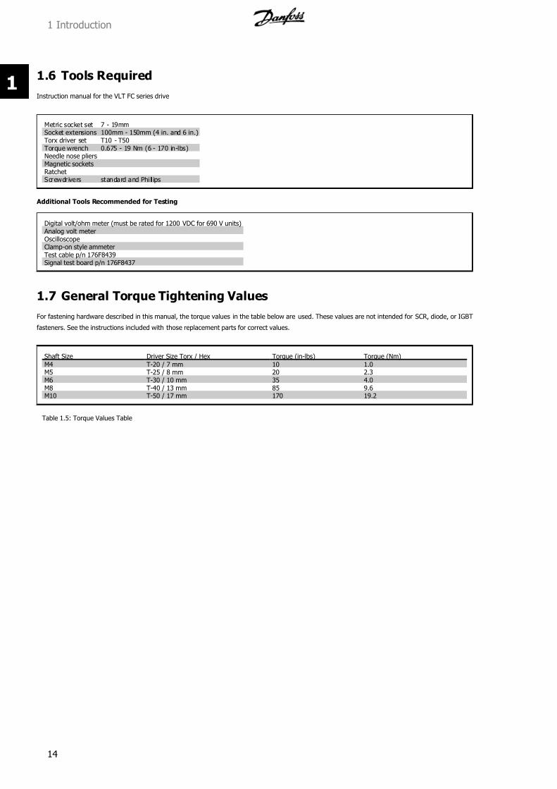
1.6 Tools Required
Instruction manual for the VLT FC series drive
Metric socket set 7 - 19mmSocket extensions 100mm - 150mm (4 in. and 6 in.)Torx driver set T10 - T50Torque wrench 0.675 - 19 Nm (6 - 170 in-lbs)Needle nose pliersMagnetic socketsRatchetScrewdrivers standard and Phill ips
Additional Tools Recommended for Testing
Digital volt/ohm meter (must be rated for 1200 VDC for 690 V units) Analog volt meterOscilloscopeClamp-on style ammeterTest cable p/n 176F8439Signal test board p/n 176F8437
1.7 General Torque Tightening Values
For fastening hardware described in this manual, the torque values in the table below are used. These values are not intended for SCR, diode, or IGBT
fasteners. See the instructions included with those replacement parts for correct values.
Shaft Size Driver Size Torx / Hex Torque (in-lbs) Torque (Nm)
M4 T-20 / 7 mm 10 1.0M5 T-25 / 8 mm 20 2.3M6 T-30 / 10 mm 35 4.0M8 T-40 / 13 mm 85 9.6M10 T-50 / 17 mm 170 19.2
Table 1.5: Torque Values Table
1 Introduction
14
1

7/16/2019 1. D & E Frame.pdf
http://slidepdf.com/reader/full/1-d-e-framepdf 15/197
1.8 Exploded Views
1 3 0
B X 1 6 7 . 1 0
1
19 13
12
25
5
4
22
21
20
18
17
3
16
15
14
11
24
2
10
9
8
76
23
Illustration 1.1: Exploded view D1 / D3 frame size
1 Introduction
15
1

7/16/2019 1. D & E Frame.pdf
http://slidepdf.com/reader/full/1-d-e-framepdf 16/197
1 Control card PCA1 14 SCR/Diode module SCR 1, 2, 32 Control input terminals 15 IGBT output bus bar3 Local Control Panel (LCP) 16 Output motor terminals TB24 Control card C option 17 Current sensor L2, L3, L45 Mounting bracket 18 Fan assembly F1 + C1 +CBL116 Power card mounting plate 19 Fan transformer TR17 Power card PCA 3 20 Main AC power input terminals TB18 Capacitor bank assembly CBANK1 + PCA9 21 AC input bus bar9 Soft charge fuses 22 Input terminal mounting plate assembly10 Soft charge card PCA11 23 Fan fuse FU411 DC inductor L1 24 Capacitor bank cover plate12 Soft charge module R1 + CBL26 25 IGBT gate driver card PCA513 IGBT module IGBT 1
1 Introduction
16
1
7/16/2019 1. D & E Frame.pdf
http://slidepdf.com/reader/full/1-d-e-framepdf 17/197
1 3 0 B X 1 6 6 . 1 0
4
1
2
3
5
6 7
11
10
9
8
12
15
14
13
16
20
19
18
17
21
22
28
27
26
25
24
23
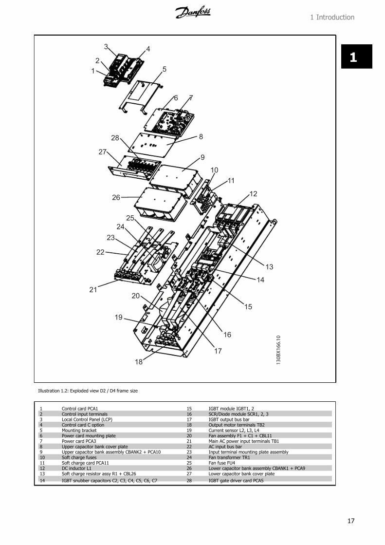
Illustration 1.2: Exploded view D2 / D4 frame size
1 Control card PCA1 15 IGBT module IGBT1, 22 Control input terminals 16 SCR/Diode module SCR1, 2, 33 Local Control Panel (LCP) 17 IGBT output bus bar4 Control card C option 18 Output motor terminals TB25 Mounting bracket 19 Current sensor L2, L3, L46 Power card mounting plate 20 Fan assembly F1 + C1 + CBL117 Power card PCA3 21 Main AC power input terminals TB18 Upper capacitor bank cover plate 22 AC input bus bar9 Upper capacitor bank assembly CBANK2 + PCA10 23 Input terminal mounting plate assembly10 Soft charge fuses 24 Fan transformer TR111 Soft charge card PCA11 25 Fan fuse FU412 DC inductor L1 26 Lower capacitor bank assembly CBANK1 + PCA913 Soft charge resistor assy R1 + CBL26 27 Lower capacitor bank cover plate
14 IGBT snubber capacitors C2, C3, C4, C5, C6, C7 28 IGBT gate driver card PCA5
1 Introduction
17
1

7/16/2019 1. D & E Frame.pdf
http://slidepdf.com/reader/full/1-d-e-framepdf 18/197
1 3 0 B X 1 6 8 . 1 0
3
20
19 18
17
16
15
1
14
13
12
1110
2
9
8
76
5
4
25
2423
2221
Illustration 1.3: Exploded view E1 / E2 frame size
1 Control card PCA1 14 SCR and Diode SCR1, SCR2, SCR3 and D1, D2, D32 Control input terminals 15 Fan inductor (not on all units)3 Local Control Panel (LCP) 16 Soft charge resistor assy R14 Control card C option 17 IGBT output bus bar5 Mounting bracket 18 Fan assembly F1 + C16 Power card mounting plate 19 Output motor terminals TB27 Power card PCA3 20 Current sensor L2, L3, L48 IGBT gate driver card PCA5 21 Main AC power input terminals TB19 Upper capacitor bank assembly CBANK2 + PCA11 22 Input terminal mounting plate assembly10 Soft charge fuses 23 AC input bus bar11 DC inductor L1 24 Soft charge card PCA1212 Fan transformer TR1 25 Lower capacitor bank assembly CBANK1 + PCA1013 IGBT module IGBT1, 2, 3
1 Introduction
18
1
7/16/2019 1. D & E Frame.pdf
http://slidepdf.com/reader/full/1-d-e-framepdf 19/197
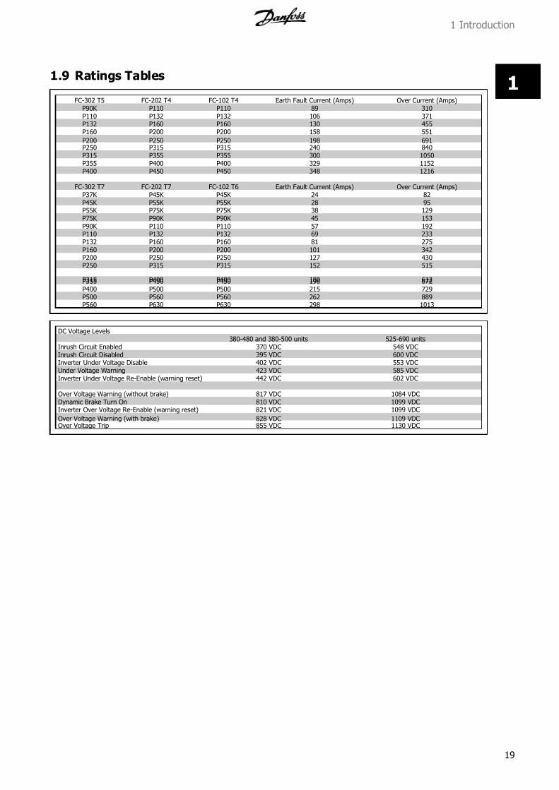
1.9 Ratings Tables
FC-302 T5 FC-202 T4 FC-102 T4 Earth Fault Current (Amps) Over Current (Amps)P90K P110 P110 89 310P110 P132 P132 106 371P132 P160 P160 130 455P160 P200 P200 158 551
P200 P250 P250 198 691P250 P315 P315 240 840P315 P355 P355 300 1050P355 P400 P400 329 1152P400 P450 P450 348 1216
FC-302 T7 FC-202 T7 FC-102 T6 Earth Fault Current (Amps) Over Current (Amps)
P37K P45K P45K 24 82P45K P55K P55K 28 95P55K P75K P75K 38 129P75K P90K P90K 45 153P90K P110 P110 57 192P110 P132 P132 69 233P132 P160 P160 81 275P160 P200 P200 101 342P200 P250 P250 127 430P250 P315 P315 152 515
P315 P400 P400 180 612P355 P450 P450 198 672P400 P500 P500 215 729P500 P560 P560 262 889P560 P630 P630 298 1013
DC Voltage Levels380-480 and 380-500 units 525-690 units
Inrush Circuit Enabled 370 VDC 548 VDCInrush Circuit Disabled 395 VDC 600 VDCInverter Under Voltage Disable 402 VDC 553 VDCUnder Voltage Warning 423 VDC 585 VDCInverter Under Voltage Re-Enable (warning reset) 442 VDC 602 VDC Over Voltage Warning (without brake) 817 VDC 1084 VDCDynamic Brake Turn On 810 VDC 1099 VDCInverter Over Voltage Re-Enable (warning reset) 821 VDC 1099 VDC
Over Voltage Warning (with brake) 828 VDC 1109 VDCOver Voltage Trip 855 VDC 1130 VDC
1 Introduction
19
1
7/16/2019 1. D & E Frame.pdf
http://slidepdf.com/reader/full/1-d-e-framepdf 20/197
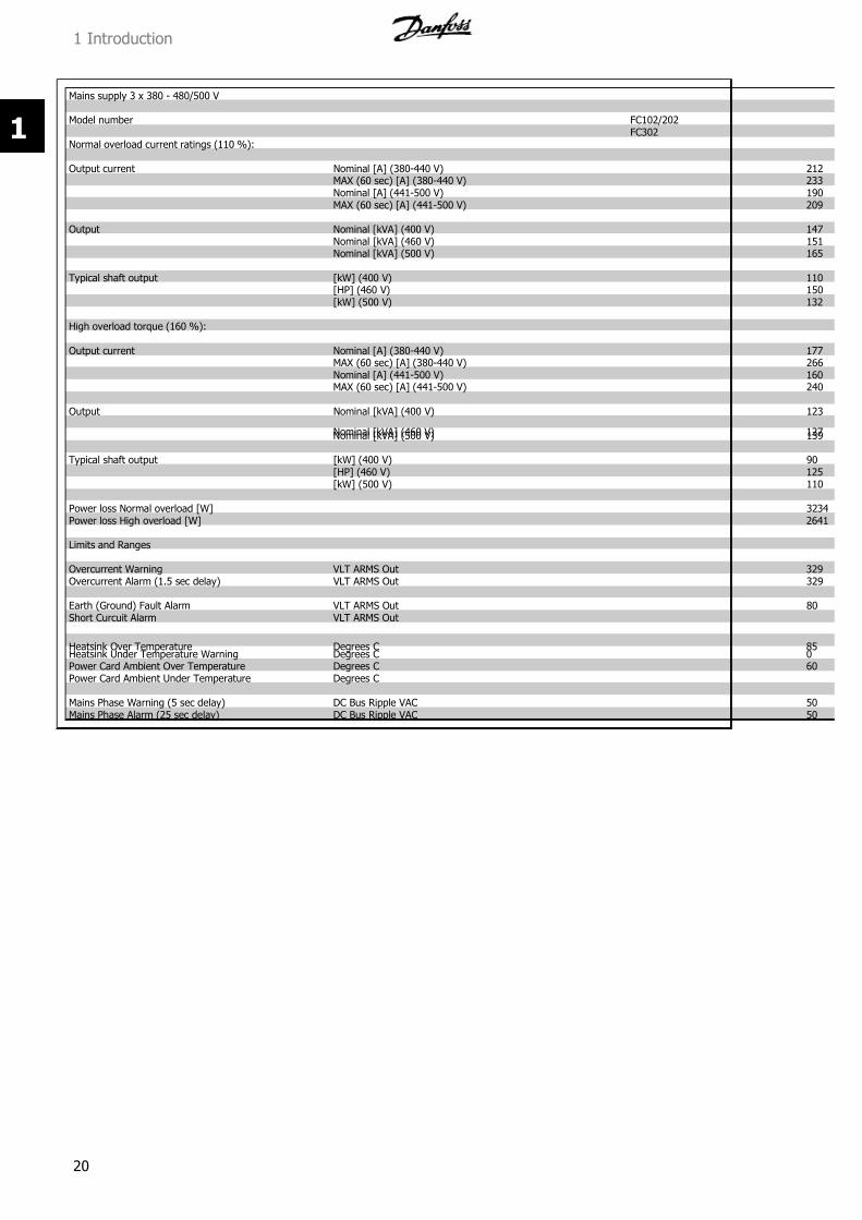
Mains supply 3 x 380 - 480/500 V
Model number FC102/202FC302
Normal overload current ratings (110 %):
Output current Nominal [A] (380-440 V) 212MAX (60 sec) [A] (380-440 V) 233Nominal [A] (441-500 V) 190MAX (60 sec) [A] (441-500 V) 209
Output Nominal [kVA] (400 V) 147
Nominal [kVA] (460 V) 151Nominal [kVA] (500 V) 165
Typical shaft output [kW] (400 V) 110
[HP] (460 V) 150[kW] (500 V) 132
High overload torque (160 %):
Output current Nominal [A] (380-440 V) 177MAX (60 sec) [A] (380-440 V) 266Nominal [A] (441-500 V) 160MAX (60 sec) [A] (441-500 V) 240
Output Nominal [kVA] (400 V) 123
Nominal [kVA] (460 V) 127Nominal [kVA] (500 V) 139 Typical shaft output [kW] (400 V) 90
[HP] (460 V) 125[kW] (500 V) 110
Power loss Normal overload [W] 3234Power loss High overload [W] 2641
Limits and Ranges
Overcurrent Warning VLT ARMS Out 329Overcurrent Alarm (1.5 sec delay) VLT ARMS Out 329
Earth (Ground) Fault Alarm VLT ARMS Out 80Short Curcuit Alarm VLT ARMS Out
Heatsink Over Temperature Degrees C 85Heatsink Under Temperature Warning Degrees C 0Power Card Ambient Over Temperature Degrees C 60Power Card Ambient Under Temperature Degrees C
Mains Phase Warning (5 sec delay) DC Bus Ripple VAC 50Mains Phase Alarm (25 sec delay) DC Bus Ripple VAC 50
1 Introduction
20
1

7/16/2019 1. D & E Frame.pdf
http://slidepdf.com/reader/full/1-d-e-framepdf 21/197
Mains supply 3 x 380 - 480/500 V
Model number
Normal overload current ratings (110 %):
Output current Nominal [A]
(380-440 V)
MAX (60 sec) [A]
(380-440 V)
Nominal [A]
(441-500 V)
MAX (60 sec) [A]
(441-500 V)
Output Nominal [kVA]
(400 V)
Nominal [kVA]
(460 V)
Nominal [kVA]
(500 V)
Typical shaft output [kW] (400 V)
[HP] (460 V)
[kW] (500 V)
High overload torque (160 %):
Output current Nominal [A]
(380-440 V)
MAX (60 sec) [A]
(380-440 V)
Nominal [A]
(441-500 V)
MAX (60 sec) [A]
(441-500 V)
Output Nominal [kVA]
(400 V)
Nominal [kVA]
(460 V)
Nominal [kVA]
(500 V)
Typical shaft output [kW] (400 V)
[HP] (460 V)
[kW] (500 V)
Power loss Normal overload [W]
Power loss High overload [W]
Limits and Ranges
Overcurrent Warning VLT ARMS Out
Overcurrent Alarm (1.5 sec delay) VLT ARMS Out
Earth (Ground) Fault Alarm VLT ARMS OutShort Curcuit Alarm VLT ARMS Out
Heatsink Over Temperature Degrees C
Heatsink Under Temperature Warning Degrees C
Power Card Ambient Over Temperature Degrees C
Power Card Ambient Under Temperature Degrees C
Mains Phase Warning (5 sec delay) DC Bus Ripple VAC
1 Introduction
21
1

7/16/2019 1. D & E Frame.pdf
http://slidepdf.com/reader/full/1-d-e-framepdf 22/197
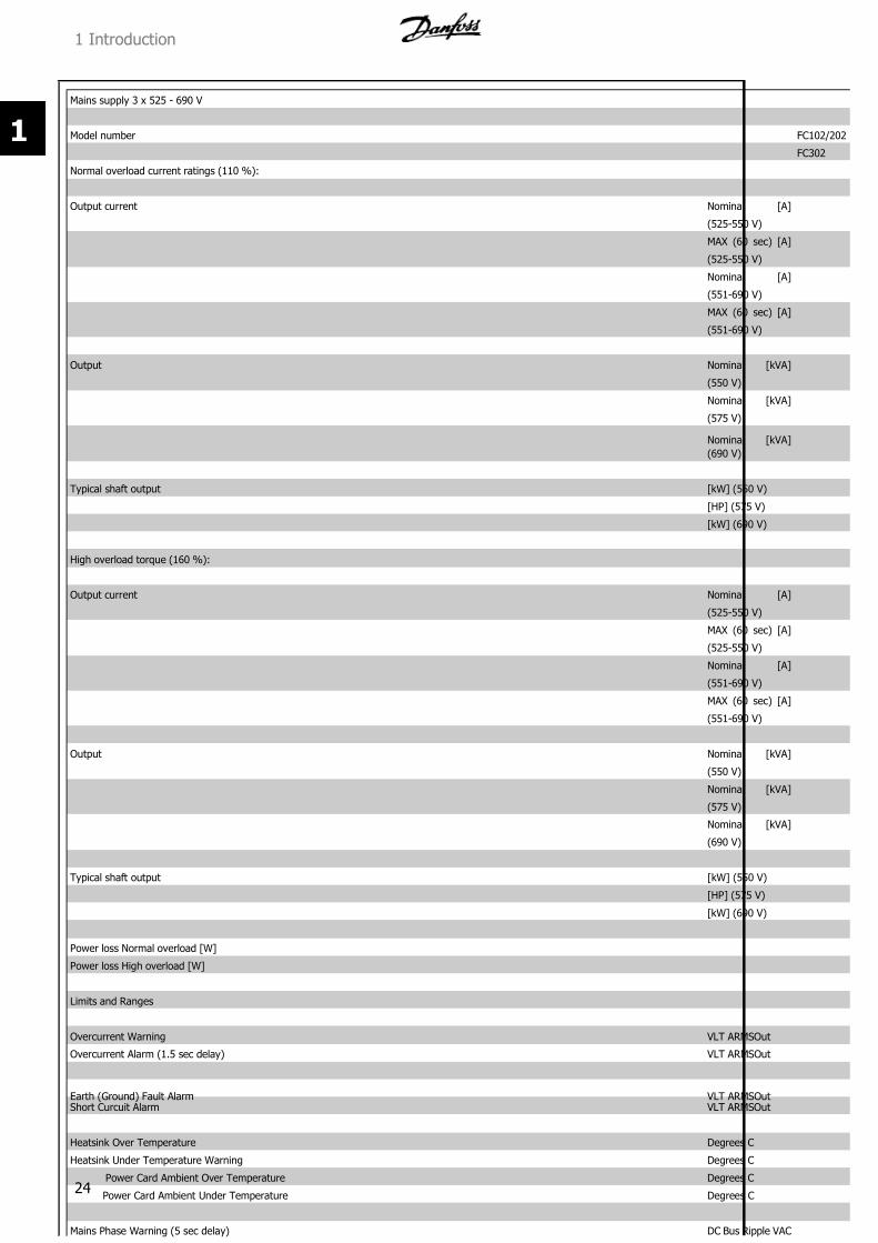
Mains supply 3 x 525 - 690 V
Model number
Normal overload current ratings (110 %):
Output current Nominal [A]
(525-550 V)
MAX (60 sec) [A]
(525-550 V)
Nominal [A]
(551-690 V)
MAX (60 sec) [A]
(551-690 V)
Output Nominal [kVA]
(550 V)
Nominal [kVA]
(575 V)
Nominal [kVA]
(690 V)
Typical shaft output [kW] (550 V)
[HP] (575 V)
[kW] (690 V)
High overload torque (160 %):
Output current Nominal [A]
(525-550 V)
MAX (60 sec) [A]
(525-550 V)
Nominal [A]
(551-690 V)
MAX (60 sec) [A]
(551-690 V)
Output Nominal [kVA]
(550 V)
Nominal [kVA]
(575 V)
Nominal [kVA]
(690 V)
Typical shaft output [kW] (550 V)
[HP] (575 V)
[kW] (690 V)
Power loss Normal overload [W]
Power loss High overload [W]
Limits and Ranges
Overcurrent Warning VLT ARMS Out
Overcurrent Alarm (1.5 sec delay) VLT ARMS Out
Earth (Ground) Fault Alarm VLT ARMS OutShort Curcuit Alarm VLT ARMS Out
Heatsink Over Temperature Degrees C
Heatsink Under Temperature Warning Degrees C
Power Card Ambient Over Temperature Degrees C
Power Card Ambient Under Temperature Degrees C
Mains Phase Warning (5 sec delay) DC Bus Ripple VAC
1 Introduction
22
1

7/16/2019 1. D & E Frame.pdf
http://slidepdf.com/reader/full/1-d-e-framepdf 23/197
Mains supply 3 x 525-690 V
Model number
Normal overload current ratings (110 %):
Output current Nominal [A]
(525-550 V)
MAX (60 sec) [A]
(525-550 V)
Nominal [A]
(551-690 V)
MAX (60 sec) [A]
(551-690 V)
Output Nominal [kVA]
(550 V)
Nominal [kVA]
(575 V)
Nominal [kVA]
(690 V)
Typical shaft output [kW] (550 V)
[HP] (575 V)
[kW] (690 V)
High overload torque (160 %):
Output current Nominal [A]
(525-550 V)
MAX (60 sec) [A]
(525-550 V)
Nominal [A]
(551-690 V)
MAX (60 sec) [A]
(551-690 V)
Output Nominal [kVA]
(550 V)
Nominal [kVA]
(575 V)
Nominal [kVA]
(690 V)
Typical shaft output [kW] (550 V)
[HP] (575 V)
[kW] (690 V)
Power loss Normal overload [W]
Power loss High overload [W]
Limits and Ranges
Overcurrent Warning VLT ARMS Out
Overcurrent Alarm (1.5 sec delay) VLT ARMS Out
Earth (Ground) Fault Alarm VLT ARMS Out
Short Curcuit Alarm VLT ARMS Out
Heatsink Over Temperature Degrees C
Heatsink Under Temperature Warning Degrees C
Power Card Ambient Over Temperature Degrees C
Power Card Ambient Over Temperature Degrees C
1 Introduction
23
1
7/16/2019 1. D & E Frame.pdf
http://slidepdf.com/reader/full/1-d-e-framepdf 24/197
Mains supply 3 x 525 - 690 V
Model number FC102/202
FC302
Normal overload current ratings (110 %):
Output current Nominal [A]
(525-550 V)
MAX (60 sec) [A]
(525-550 V)
Nominal [A]
(551-690 V)
MAX (60 sec) [A]
(551-690 V)
Output Nominal [kVA]
(550 V)
Nominal [kVA]
(575 V)
Nominal [kVA]
(690 V)
Typical shaft output [kW] (550 V)
[HP] (575 V)
[kW] (690 V)
High overload torque (160 %):
Output current Nominal [A]
(525-550 V)
MAX (60 sec) [A]
(525-550 V)
Nominal [A]
(551-690 V)
MAX (60 sec) [A]
(551-690 V)
Output Nominal [kVA]
(550 V)
Nominal [kVA]
(575 V)
Nominal [kVA]
(690 V)
Typical shaft output [kW] (550 V)
[HP] (575 V)
[kW] (690 V)
Power loss Normal overload [W]
Power loss High overload [W]
Limits and Ranges
Overcurrent Warning VLT ARMSOut
Overcurrent Alarm (1.5 sec delay) VLT ARMSOut
Earth (Ground) Fault Alarm VLT ARMSOutShort Curcuit Alarm VLT ARMSOut
Heatsink Over Temperature Degrees C
Heatsink Under Temperature Warning Degrees C
Power Card Ambient Over Temperature Degrees C
Power Card Ambient Under Temperature Degrees C
Mains Phase Warning (5 sec delay) DC Bus Ripple VAC
1 Introduction
24
1

7/16/2019 1. D & E Frame.pdf
http://slidepdf.com/reader/full/1-d-e-framepdf 25/197
2 Operator Interface and Drive Control
2.1 Introduction
VLT drives are designed with self-diagnostic circuitry to isolate fault conditions and activate display messages which greatly simplify troubleshooting and
service. The operating status of the drive is displayed in real-time. Virtually every command given to the drive results in some indication on the local
control panel (LCP) display. Fault logs are maintained within the drive for fault history.
The drive monitors supply and output voltages along with the operational condition of the motor and load. When the drive issues a warning or alarm, it
cannot be assumed that the fault lies within the drive itself. In fact, for most service calls, the fault condition will be found outside of the drive. Most of
the warnings and alarms that the drive displays are generated by response to faults outside of the drive. This service manual provides techniques and
test procedures to help isolate a fault condition whether in the drive or elsewhere.
Familiarity with the information provided on the display is important. Additional diagnostic data can be accessed easily through the LCP.
2.2 User Interface
2.2.1 How to operate the graphic local control panel (LCP)
The LCP keypad is divided into four functional groups:
1. Graphical display with Status lines.
2. Menu keys and indicator lights (LEDs) - selecting mode, changing parameters and switching between display functions.
3. Navigation keys and indicator lights (LEDs).
4. Operation keys and indicator lights (LEDs).
Graphical display:
The LCD display is back-lit with a total of 6 alpha-numeric lines. All data is displayed on the LCP which can show up to five operating variables while in
[Status] mode.
2 Operator Interface and Drive Control
25
2

7/16/2019 1. D & E Frame.pdf
http://slidepdf.com/reader/full/1-d-e-framepdf 26/197
Display lines:
a. Status line: Status messages displaying icons and graphics.
b. Line 1-2: Operator data lines displaying data and variables de-
fined or chosen by the user. By pressing the [Status] key, up to
one extra line can be added.
c. Status line: Status messages displaying text.
The display is divided into three sections:
Top section (a) shows the status when in status mode or up to two variables when not in status mode and in the case of Alarm/Warning.
The number of the Active Set-up (selected as the Active Set-up in par. 0-10) is shown. When programming in another Set-up than the Active Set-up, the
number of the Set-up being programmed appears to the right in brackets.
The Middle section (b) shows up to 5 variables with related unit, regardless of status. In case of alarm/warning, the warning is shown instead of the
variables.
It is possible to toggle between three status readout displays by pressing the [Status] key.
Operating variables with different formatting are shown in each status screen - see below.
Several values or measurements can be linked to each of the displayed operating variables. The values / measurements to be displayed can be defined
via par. 0-20, 0-21, 0-22, 0-23, and 0-24, which can be accessed via [QUICK MENU], "Q3 Function Setups", "Q3-1 General Settings", "Q3-13 Display
Settings".
Each value / measurement readout parameter selected in par. 0-20 to par. 0-24 has its own scale and number of digits after a possible decimal point.
Larger numeric values are displayed with few digits after the decimal point.
Ex.: Current readout
5.25 A; 15.2 A 105 A.
2 Operator Interface and Drive Control
26
2

7/16/2019 1. D & E Frame.pdf
http://slidepdf.com/reader/full/1-d-e-framepdf 27/197
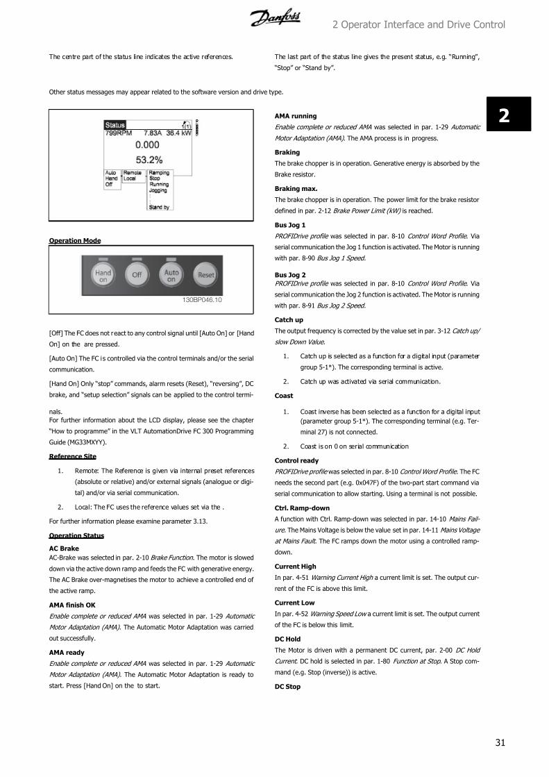
Status display I:
This readout state is standard after start-up or initialization.
Use [INFO] to obtain information about the value/measurement linked to
the displayed operating variables (1.1, 1.2, 1.3, 2, and 3).
See the operating variables shown in the display in this illustration. 1.1,
1.2 and 1.3 are shown in small size. 2 and 3 are shown in medium size. 1 3 0 B P 0 4 1
. 1 0
1.1
1.3
2
1.2
3
Status display II:
See the operating variables (1.1, 1.2, 1.3, and 2) shown in the display in
this illustration.
In the example, Speed, Motor current, Motor power and Frequency are
selected as variables in the first and second lines.
1.1, 1.2 and 1.3 are shown in small size. 2 is shown in large size.
1 3 0 B P 0 6 2
. 1 0
2
1.2
1.31.1
Status display III:
This state displays the event and action of the Smart Logic Control.
1 3 0 B
P 0 6 3
. 1 0
The Bottom section always shows the state of the drive in Status mode.
Display contrast adjustment
Press [status] and [] for darker display
Press [status] and [] for brighter display
1 3 0 B P 0 7 4
. 1 0
Top section
Middle section
Bottom section
2 Operator Interface and Drive Control
27
2

7/16/2019 1. D & E Frame.pdf
http://slidepdf.com/reader/full/1-d-e-framepdf 28/197
Indicator lights (LEDs):
If certain threshold values are exceeded, the alarm and/or warning LED lights up. A status and alarm text appear on the control panel.
The On LED is activated when the drive receives power from mains voltage, a DC bus terminal, or an external 24 V supply. At the same time, the back
light is on.
• Green LED/On: Control section is working.
• Yellow LED/Warn.: Indicates a warning.
• Flashing Red LED/Alarm: Indicates an alarm.
LCP keys
Menu keys
The menu keys are divided into functions. The keys below the display and
indicator lamps are used for parameter set-up, including choice of display
indication during normal operation.130BP045.10
[Status]
indicates the status of the drive and/or the motor. Three different readouts can be chosen by pressing the [Status] key:
5 line readouts, 4 line readouts or Smart Logic Control.
Use [Status] for selecting the mode of display or for changing back to Display mode from either the Quick Menu mode, the Main Menu mode or Alarm
mode. Also use the [Status] key to toggle single or double read-out mode.
[Quick Menu]
allows quick set-up of the drive. The most common functions can be programmed here.
The [Quick Menu] consists of:
- My Personal Menu
- Quick Set-up
- Function set-up
- Changes Made
- Loggings
The Function set-up provides quick and easy access to all parameters required for the majority of applications. Among other features it also includes
parameters for selecting which variables to display on the LCP.
[Main Menu]
is used for programming all parameters. The Main Menu parameters can be accessed immediately unless a password has been created via par. 0-60,
0-61, 0-65 or 0-66.
Parameter shortcut can be carried out by pressing down the [Main Menu] key for 3 seconds. The parameter shortcut allows direct access to any
parameter.
2 Operator Interface and Drive Control
28
2

7/16/2019 1. D & E Frame.pdf
http://slidepdf.com/reader/full/1-d-e-framepdf 29/197
[Alarm Log]
displays an Alarm list of the five latest alarms (numbered A1-A5). To obtain additional details about an alarm, use the arrow keys to find the alarm number
and press [OK]. Information is displayed about the condition of the drive before it enters the alarm mode.
The Alarm log button on the LCP allows access to both Alarm log and Maintenance log.
[Back]
reverts to the previous step or layer in the navigation structure.
[Cancel]
last change or command will be cancelled as long as the display has not been changed.
[Info]
displays information about a command, parameter, or function in any display window. [Info] provides detailed information when needed.
Exit Info mode by pressing either [Info], [Back], or [Cancel].
Navigation keys
The four navigation arrows are used to navigate between the different
choices available in [Quick Menu], [Main Menu] and [Alarm Log].
Use the keys to move the cursor.
[OK] is used for choosing a parameter marked by the cursor and for
enabling the change of a parameter.
Operation keys for local control are found at the bottom of the control
panel.
130BP046.10
[Hand On]
enables control of the drive via the LCP. [Hand on] also starts the motor, and it is now possible to enter the motor speed data by means of the arrow
keys. The key can be selected as Enable [1] or Disable [0] via par. 0-40 [Hand on] key on LCP.
The following control signals will still be active when [Hand on] is activated:
• [Hand on] - [Off] - [Auto on]
• Reset
2 Operator Interface and Drive Control
29
2
7/16/2019 1. D & E Frame.pdf
http://slidepdf.com/reader/full/1-d-e-framepdf 30/197
• Coasting stop inverse
• Reversing
• Set-up select lsb - Set-up select msb
• Stop command from serial communication
• Quick stop
• DC brake
NB!
External stop signals activated by means of control signals or a serial bus will override a “start” command via the LCP.
[Off]
stops the connected motor. The key can be selected as Enable [1] or Disable [0] via par. 0-41 [Off] key on LCP. If no external stop function is selected
and the [Off] key is inactive the motor can only be stopped by disconnecting the mains supply.
[Auto On]
enables the drive to be controlled via the control terminals and/or serial communication. When a start signal is applied on the control terminals and/orthe bus, the drive will start. The key can be selected as Enable [1] or Disable [0] via par. 0-42 [Auto on] key on LCP.
NB!
An active HAND-OFF-AUTO signal via the digital inputs has higher priority than the control keys [Hand on] – [Auto on].
[Reset]
is used for resetting the drive after an alarm (trip). It can be selected as Enable [1] or Disable [0] via par. 0-43 Reset Keys on LCP .
The parameter shortcut can be carried out by holding down the [Main Menu] key for 3 seconds. The parameter shortcut allows direct access to any
parameter.
2.2.2 Numeric Local Control Panel (NLCP)
See the operator's manual for instructions for using the numeric LCP.
2.2.3 Tips and tricks
* For the majority of applications the Quick Menu, Quick Set-up and Function Set-up provides the simplest and quickest accessto all the typical parameters required.
* Whenever possible, performing an AMA, will ensure best shaft performance* Contrast of the display can be adjusted by pressing [Status] and [] for darker display or by pressing [Status] and [] for
brighter dispaly* Under [Quick Menu] and [Changes Made] all parameters that have been changed from factory settings are displayed* Press and hold [Main Menu] key for 3 seconds for access to any parameter* For service purposes it is recommended to copy all parameters to the , see par. for further information
Table 2.1: Tips and tricks
2.3 Status Messages
2.3.1 Status Messages
Status messages appear in the bottom of the display - see example below. The left part of the status line indicates the active type of control of thefrequency converter.
2 Operator Interface and Drive Control
30
2
7/16/2019 1. D & E Frame.pdf
http://slidepdf.com/reader/full/1-d-e-framepdf 31/197
The centre part of the status line indicates the active references. The last part of the status line gives the present status, e.g. “Running”,
“Stop” or “Stand by”.
Other status messages may appear related to the software version and drive type.
Operation Mode
130BP046.10
[Off] The FC does not react to any control signal until [Auto On] or [Hand
On] on the are pressed.
[Auto On] The FC is controlled via the control terminals and/or the serial
communication.
[Hand On] Only “stop” commands, alarm resets (Reset), “reversing”, DC
brake, and “setup selection” signals can be applied to the control termi-
nals.
For further information about the LCD display, please see the chapter
“How to programme” in the VLT AutomationDrive FC 300 Programming
Guide (MG33MXYY).
Reference Site
1. Remote: The Reference is given via internal preset references
(absolute or relative) and/or external signals (analogue or digi-
tal) and/or via serial communication.
2. Local: The FC uses the reference values set via the .
For further information please examine parameter 3.13.
Operation Status
AC Brake
AC-Brake was selected in par. 2-10 Brake Function . The motor is slowed
down via the active down ramp and feeds the FC with generative energy.
The AC Brake over-magnetises the motor to achieve a controlled end of
the active ramp.
AMA finish OK
Enable complete or reduced AMA was selected in par. 1-29 Automatic
Motor Adaptation (AMA) . The Automatic Motor Adaptation was carried
out successfully.
AMA ready
Enable complete or reduced AMA was selected in par. 1-29 Automatic
Motor Adaptation (AMA) . The Automatic Motor Adaptation is ready to
start. Press [Hand On] on the to start.
AMA running
Enable complete or reduced AMA was selected in par. 1-29 Automatic
Motor Adaptation (AMA) . The AMA process is in progress.
Braking
The brake chopper is in operation. Generative energy is absorbed by the
Brake resistor.
Braking max.
The brake chopper is in operation. The power limit for the brake resistor
defined in par. 2-12 Brake Power Limit (kW) is reached.
Bus Jog 1
PROFIDrive profile was selected in par. 8-10 Control Word Profile . Via
serial communication the Jog 1 function is activated. The Motor is running
with par. 8-90 Bus Jog 1 Speed .
Bus Jog 2
PROFIDrive profile was selected in par. 8-10 Control Word Profile . Via
serial communication the Jog 2 function is activated. The Motor is running
with par. 8-91 Bus Jog 2 Speed .
Catch up
The output frequency is corrected by the value set in par. 3-12 Catch up/
slow Down Value .
1. Catch up is selected as a function for a digital input (parameter
group 5-1*). The corresponding terminal is active.
2. Catch up was activated via serial communication.
Coast
1. Coast inverse has been selected as a function for a digital input
(parameter group 5-1*). The corresponding terminal (e.g. Ter-
minal 27) is not connected.
2. Coast is on 0 on serial communication
Control ready
PROFIDrive profile was selected in par. 8-10 Control Word Profile . The FC
needs the second part (e.g. 0x047F) of the two-part start command via
serial communication to allow starting. Using a terminal is not possible.
Ctrl. Ramp-down
A function with Ctrl. Ramp-down was selected in par. 14-10 Mains Fail-
ure . The Mains Voltage is below the value set in par. 14-11 Mains Voltage
at Mains Fault . The FC ramps down the motor using a controlled ramp-
down.
Current High
In par. 4-51 Warning Current High a current limit is set. The output cur-
rent of the FC is above this limit.
Current Low
In par. 4-52 Warning Speed Low a current limit is set. The output current
of the FC is below this limit.
DC Hold
The Motor is driven with a permanent DC current, par. 2-00 DC Hold
Current . DC hold is selected in par. 1-80 Function at Stop . A Stop com-
mand (e.g. Stop (inverse)) is active.
DC Stop
2 Operator Interface and Drive Control
31
2
7/16/2019 1. D & E Frame.pdf
http://slidepdf.com/reader/full/1-d-e-framepdf 32/197
The Motor is momentarily driven with a DC current, par. 2-01 DC Brake
Current , for a specified time, par. 2-02 DC Braking Time .
1. DC-Brake is activated (OFF) in par. 2-03 DC Brake Cut In Speed
[RPM] and a Stop command (e.g. Stop (inverse)) is active.
2. DC Brake (inverse) is selected as a function for a digital input
(parameter group 5-1*). The corresponding terminal is not ac-
tive.
3. The DC Brake is activated via serial communication.
DC Voltage U0
In par. 1-01 Motor Control Principle U/f and in par. 1-80 Function at
Stop DC-Voltage U0 is selected. A Stop command (e.g. Stop (inverse)) is
activated. The Voltage selected according to the par. 1-55 U/f Charac-
teristic - U [0] (U/f-Characteristic – U[V]) is applied to the Motor.
Feedback high
In par. 4-57 Warning Feedback High an upper Feedback limit is set. The
sum of all active feedbacks (parameter group 7-2*) is above the feedback
limit.
Feedback low
In par. 4-56 Warning Feedback Low a lower Feedback limit is set. The
sum of all active feedbacks (parameter group 7-2*) is below the feedback
limit.
Flying start
In par. 1-73 Flying Start the Flying start function is activated. The FC is
testing if the connected Motor is running with a speed that is in the ad-
justed speed range. The process was started by connecting a digital input
(parameter group 5-1*) programmed as Coast inverse or by connecting
the Mains.
Freeze output
The remote reference is active and the momentarily given speed is saved.
1. Freeze output was selected as a function for a digital input(Group 5-1*). The corresponding terminal is active. Speed con-
trol is only possible via the terminal functions Speed up and
Speed down.
2. Hold ramp is activated via serial communication.
Freeze output request
A freeze output command has been given, but the motor will remain
stopped until a Run permissive signal is received via a digital input.
Freeze Ref.
Freeze Ref. was chosen as a function for a digital input (parameter group
5-1*). The corresponding terminal is controlled. The FC saves the actual
reference. Changing the reference is now only possible via terminal func-
tions Speed up and Speed down.
Jog request
A JOG command has been given, bur the motor will be stopped until a
Run permissive signal is received via a digital input.
Jogging
The Motor is running with par. 3-19 Jog Speed [RPM] .
1. Jog was selected as function for a digital input (parameter group
5-1*). The corresponding terminal (e.g. Terminal 29) is active.
2. The Jog function is activated via the serial communication.
3. The Jog function was selected as a reaction for a monitoring
function (e.g. No signal). The monitoring function is active.
Kinetic back-up
In par. 14-10 Mains Failure a function was set as Kinetic back-up. The
Mains Voltage is below the value set in par. 14-11 Mains Voltage at Mains
Fault . The FC is running the motor momentarily with kinetic energy from
the inertia of the load.
Motor check (FC 100/200 only)
In par. 1-80 Function at Stop the function Motor check was selected. A
stop command (e.g. Stop inverse) is active. To ensure, that a Motor is
connected to the FC a permanent test current is applied to the Motor.
Off1
PROFIDrive profile was selected in par. 8-10 Control Word Profile . Via
serial communication the OFF 1 function is activated. The Motor is stop-
ped via the ramp.
Off2
PROFIDrive profile was selected in par. 8-10 Control Word Profile . Via
serial communication the OFF 2 function is activated. The output of the
FC is disabled immediately and the motor coasted.
Off3
PROFIDrive profile was selected in par. 8-10 Control Word Profile . Via
serial communication the OFF 3 function is activated. The Motor is stop-
ped via the ramp.
OVC control
Over Voltage Control is activated in par. 2-17 Over-voltage Control . The
connected Motor is supplying the FC with generative energy. The Over
Voltage Control is adjusting the U/f ratio, to run the motor in controlled
mode and to prevent the FC from tripping.
PowerUnit Off
Only with drives with installed Option (ext. 24 V supply). The mains supply
to the drive is cut off, but the control card is still supplied with 24 V.
Premagnetise
Pre-magnetisation is selected in par. 1-80 Function at Stop . A stop com-
mand (e.g. Stop inverse) is activated. A suitable constant magnetising
current is applied to the Motor.
Protection md
The FC 100/200/300 has detected a critical status (e.g. an over current,
over voltage). To avoid the drive to trip (Alarm) the Protection Mode was
activated, which among others reduces the switching frequency to 4 kHz.
If possible, the protection mode ends after approximately 10 s. Activation
of the Protection Mode can be restricted by adjusting the par. 14-26 Trip
Delay at Inverter Fault .
QStop
The motor is stopped using a Quick stop ramp par. 3-81 Quick Stop Ramp
Time .
1. Quick stop inverse was chosen as a function for a digital input
(parameter group 5-1*). The corresponding terminal (e.g. Ter-
minal 27) is not active.
2. The Quick stop function was activated via serial communication.
Ramping
The motor is accelerating/decelerating using the active Up/Down ramp.
The reference, a limit value or a standstill is not yet reached.
Ref. high
In par. 4-55 Warning Reference High a reference high limit is set. The
sum of all active references is above the reference limit.
Ref. low
2 Operator Interface and Drive Control
32
2

7/16/2019 1. D & E Frame.pdf
http://slidepdf.com/reader/full/1-d-e-framepdf 33/197
In par. 4-55 Warning Reference High a reference low limit is set. The sum
of all active references is below the reference limit.
Run on ref.
The FC is running in the reference range. The feedback value matches
the set reference value.
Run request (FC 100/200 only)
A start command has been given, but the motor will be stopped until a
Run permissive signal is received via digital input.
Running
The Motor is driven by the FC, the ramping phase is done and the motor
revolutions are outside the "On Reference" range. Occurs when one of
the motor speed limits (Par. 4-11 / 4-12 / 4-13 or 4-14) is set, but the
maximum reference is outside this range.
Sleep Boost (FC 100/200 only)
The boost function in parameter 406Boost setpoint is enabled. This func-
tion is only possible in Closed loop operation.
Sleep Mode (FC 100/200 only)
The energy saving function in parameter 403Sleep mode timer is enabled.
This means that at present the motor has stopped, but that it will restartautomatically when required.
Slow down
The output frequency is corrected by the value set in par. 3-12 Catch up/
slow Down Value .
1. Slow down was selected as a function for a digital input (pa-
rameter group 5-1*). The corresponding terminal is active.
2. Slow down was activated via serial communication.
Speed high
In par. 4-53 Warning Speed High a value is set. The speed of the motor
is above this value.
Speed low
In par. 4-52 Warning Speed Low a value is set. The speed of the motor
is below this value.
Standby
[Auto On] The FC starts the motor at a start signal on a digital input (if
the parameter is programmed accordingly) or via serial communication.
Start delay
In par. 1-71 Start Delay , the delay of the starting time was set. A Start
command was activated and the delay time is still running. The Motor will
start after the delay time has expired.
Start fwd/rev
Enable start forward and Enable start reverse were selected as functions
for two different digital inputs (parameter group 5-1*). To start the motor
a direction dependent start signal has to be given and the corresponding
terminal has to be active.
Start inhibit
PROFIDrive profile was selected in par. 8-10 Control Word Profile . The
start inhibition is active. The FC needs the first part (e.g. 0x047E) of the
two-part start command via serial communication to allow starting. See
also operation status control ready.
Stop
[Off] was pressed on the or Stop inverse was selected as a function for
a digital input (Group 5-1*). The corresponding terminal is not active.
Trip
An alarm occurred. It is possible, provided the cause of the alarm is
cleared, to reset the alarm via a Reset signal ([Reset]-Key on the , a
control terminal or serial communication).
Trip lock
A serious alarm occurred. It is possible, provided the cause of the alarm
was cleared, to reset the alarm after the mains have been switched off
and on again. This can be done via a reset signal ([Reset] on the , a
control terminal or serial communication).
Unit/Drive not ready
PROFIDrive profile was selected in par. 8-10 Control Word Profile . A Con-
trol word is sent to the FC via serial communication with Off 1, Off 2 and
Off 3 active. Start inhibit is active. To enable start see operation status
Start inhibit.
2.4 Service Functions
Service information for the drive can be shown on display lines 3 and 4.
Included in the data are counters that tabulate operating hours, power
ups and trips; fault logs that store drive status values present at the 20
most recent events that stopped the drive; and drive nameplate data.
The service information is accessed by displaying items in the drive's
15-00 parameter group.
Parameter settings are displayed by pressing the [MAIN MENU] key on
the LCP keypad.
2 Operator Interface and Drive Control
33
2
7/16/2019 1. D & E Frame.pdf
http://slidepdf.com/reader/full/1-d-e-framepdf 34/197
130BP045.10
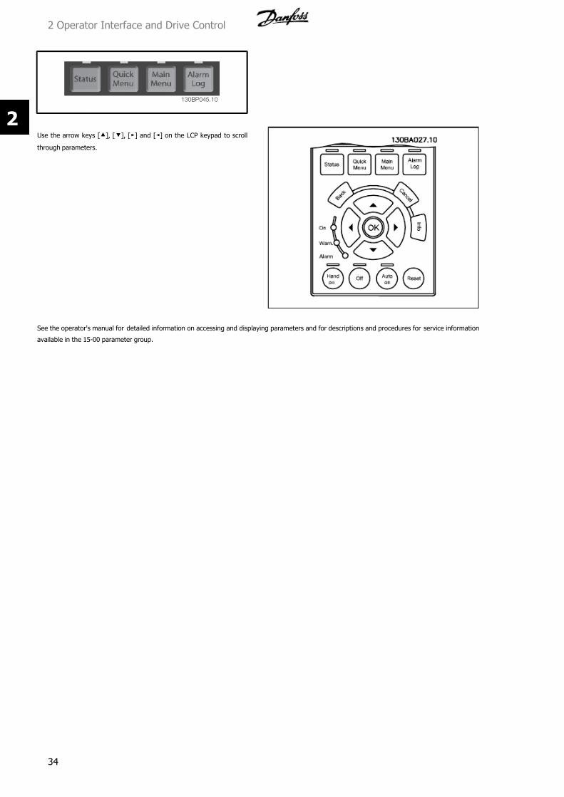
Use the arrow keys [], [], [] and [] on the LCP keypad to scroll
through parameters.
See the operator's manual for detailed information on accessing and displaying parameters and for descriptions and procedures for service information
available in the 15-00 parameter group.
2 Operator Interface and Drive Control
34
2
7/16/2019 1. D & E Frame.pdf
http://slidepdf.com/reader/full/1-d-e-framepdf 35/197
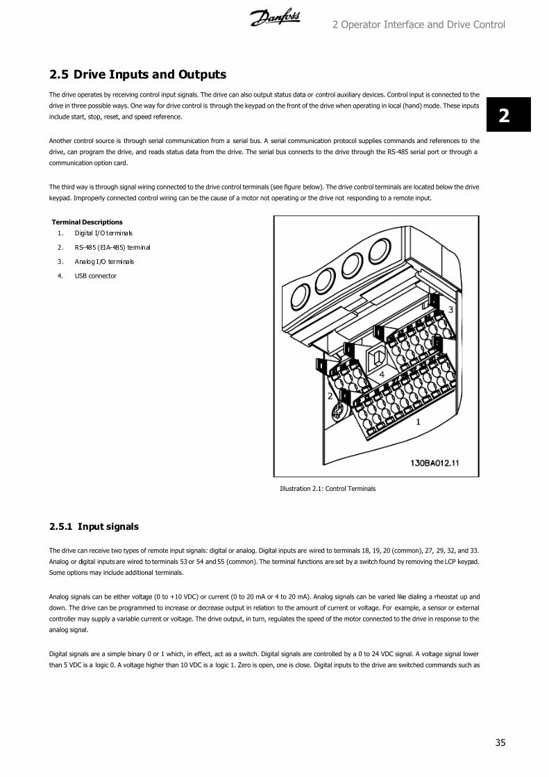
2.5 Drive Inputs and Outputs
The drive operates by receiving control input signals. The drive can also output status data or control auxiliary devices. Control input is connected to the
drive in three possible ways. One way for drive control is through the keypad on the front of the drive when operating in local (hand) mode. These inputs
include start, stop, reset, and speed reference.
Another control source is through serial communication from a serial bus. A serial communication protocol supplies commands and references to the
drive, can program the drive, and reads status data from the drive. The serial bus connects to the drive through the RS-485 serial port or through a
communication option card.
The third way is through signal wiring connected to the drive control terminals (see figure below). The drive control terminals are located below the drive
keypad. Improperly connected control wiring can be the cause of a motor not operating or the drive not responding to a remote input.
Terminal Descriptions
1. Digital I/O terminals
2. RS-485 (EIA-485) terminal
3. Analog I/O terminals
4. USB connector
Illustration 2.1: Control Terminals
2.5.1 Input signals
The drive can receive two types of remote input signals: digital or analog. Digital inputs are wired to terminals 18, 19, 20 (common), 27, 29, 32, and 33.
Analog or digital inputs are wired to terminals 53 or 54 and 55 (common). The terminal functions are set by a switch found by removing the LCP keypad.
Some options may include additional terminals.
Analog signals can be either voltage (0 to +10 VDC) or current (0 to 20 mA or 4 to 20 mA). Analog signals can be varied like dialing a rheostat up and
down. The drive can be programmed to increase or decrease output in relation to the amount of current or voltage. For example, a sensor or external
controller may supply a variable current or voltage. The drive output, in turn, regulates the speed of the motor connected to the drive in response to the
analog signal.
Digital signals are a simple binary 0 or 1 which, in effect, act as a switch. Digital signals are controlled by a 0 to 24 VDC signal. A voltage signal lower
than 5 VDC is a logic 0. A voltage higher than 10 VDC is a logic 1. Zero is open, one is close. Digital inputs to the drive are switched commands such as
2 Operator Interface and Drive Control
35
2

7/16/2019 1. D & E Frame.pdf
http://slidepdf.com/reader/full/1-d-e-framepdf 36/197
start, stop, reverse, coast, reset, and so on. (Do not confuse these digital inputs with serial communication formats where digital bytes are grouped into
communication words and protocols.)
The RS-485 serial communication connector is wired to terminals (+) 68 and (-) 69. Terminal 61 is common and may be used for terminating shields
only when the control cable run between VLT drives, not between drives and other devices. See Grounding Shielded Cables in this section for correct
methods for terminating shielded control cable.
2.5.2 Output signals
The drive also produces output signals that are carried through either the RS-485 serial bus or terminal 42. Output terminal 42 operates in the same
manner as the inputs. The terminal can be programmed for either a variable analog signal in mA or a digital signal (0 or 1) in 24 VDC. In addition, a pulse
reference can be provided on terminals 27 and 29. Output analog signals generally indicate the drive frequency, current, torque and so on to an external
controller or system. Digital outputs can be control signals used to open or close a damper, for example, or send a start or stop command to auxiliary
equipment.
Additional terminals are Form C relay outputs on terminals 01, 02, and 03, and terminals 04, 05, and 06.
Terminals 12 and 13 provide 24 VDC low voltage power, often used to supply power to the digital input terminals (18-33). Those terminals must be
supplied with power from either terminal 12 or 13, or from a customer supplied external 24 VDC power source. Improperly connected control wiring is a
common service issue for a motor not operating or the drive not responding to a remote input.
2.6 Control Terminals
Control terminals must be programmed. Each terminal has specific functions it is capable of performing and a numbered parameter associated with it.
See table below. The setting selected in the parameter enables the function of the terminal.
It is important to confirm that the control terminal is programmed for the correct function.
Parameter settings are displayed by pressing the [MAIN MENU] key on
the LCP keypad.
130BP045.10
2 Operator Interface and Drive Control
36
2

7/16/2019 1. D & E Frame.pdf
http://slidepdf.com/reader/full/1-d-e-framepdf 37/197
Use the arrow keys [], [], [] and [] on the LCP keypad to scroll
through parameters.
See the operator’s manual for details on changing parameters and the functions available for each control terminal.
In addition, the input terminal must be receiving a signal. Confirm that the control and power sources are wired to the terminal. Then check the signal.
Signals can be checked in two ways. Digital Input can be selected for display by pressing [DISPLAY MODE] key as discussed previously, or a voltmeter
may be used to check for voltage at the control terminal. See procedure details at Input Terminal Test in Section 6.
In summary, for proper drive functioning, the drive input control terminals must be:
1. wired properly
2. powered
3. programmed correctly for the intended function
4. receiving a signal
2 Operator Interface and Drive Control
37
2

7/16/2019 1. D & E Frame.pdf
http://slidepdf.com/reader/full/1-d-e-framepdf 38/197
2.7 Control Terminal Functions
The following describes the functions of the control terminals. Many of these terminals have multiple functions determined by parameter settings. Some
options provide additional terminals. See Figure 2-2.
Terminal No. Function
01, 02, 03 and 04, 05, 06 Two Form C output relays. Maximum 240 VAC, 2 A. Minimum 24 VDC, 10 mA or 24 VAC, 100 mA. Can be used for
indicating status and warnings. Physically located on power card.
12, 13 24 VDC power supply to digital inputs and external transducers. The maximum output current is 200 mA.
18, 19, 27, 29, 32, 33 Digital inputs for controlling the drive. R = 2 kohm. Less than 5 V = logic 0 (open). Greater than 10 V = logic 1
(closed). Terminals 27 and 29 are programmable as digital/pulse outputs.
20 Common for digital inputs.
37 0-24 VDC input for safety stop (some units).
39 Common for analog and digital outputs.
42 Analog and digital outputs for indicating values such as frequency, reference, current and torque. The analog signal
is 0/4 to 20 mA at a maximum of 500 Ω. The digital signal is 24 VDC at a minimum of 500 Ω.
50 10 VDC, 15 mA maximum analog supply voltage for potentiometer or thermistor.
53, 54 Selectable for 0 to 10 VDC voltage input, R = 10 k Ω, or analog signals 0/4 to 20 mA at a maximum of 200 Ω. Used
for reference or feedback signals. A thermistor can be connected here.
55 Common for terminals 53 and 54.
61 RS-485 common.
68, 69 RS-485 interface and serial communication.
Term 18 19 27 29 32 33 37 53 54 42 1-3 4-6
Para 5-10 5-11 5-12 5-13 5-14 5-15 5-19 6-1* 6-2* 6-5* 5-4* 5-4*
Table 2.2: Control Terminals and Associated Parameter
2 Operator Interface and Drive Control
38
2

7/16/2019 1. D & E Frame.pdf
http://slidepdf.com/reader/full/1-d-e-framepdf 39/197
Control terminals must be programmed. Each terminal has specific functions it is capable of performing and a numbered parameter associated with it.
The setting selected in the parameter enables the function of the terminal. See the Operator's Manual for details.
Illustration 2.2: Control Terminals Electrical Diagram
2 Operator Interface and Drive Control
39
2
7/16/2019 1. D & E Frame.pdf
http://slidepdf.com/reader/full/1-d-e-framepdf 40/197
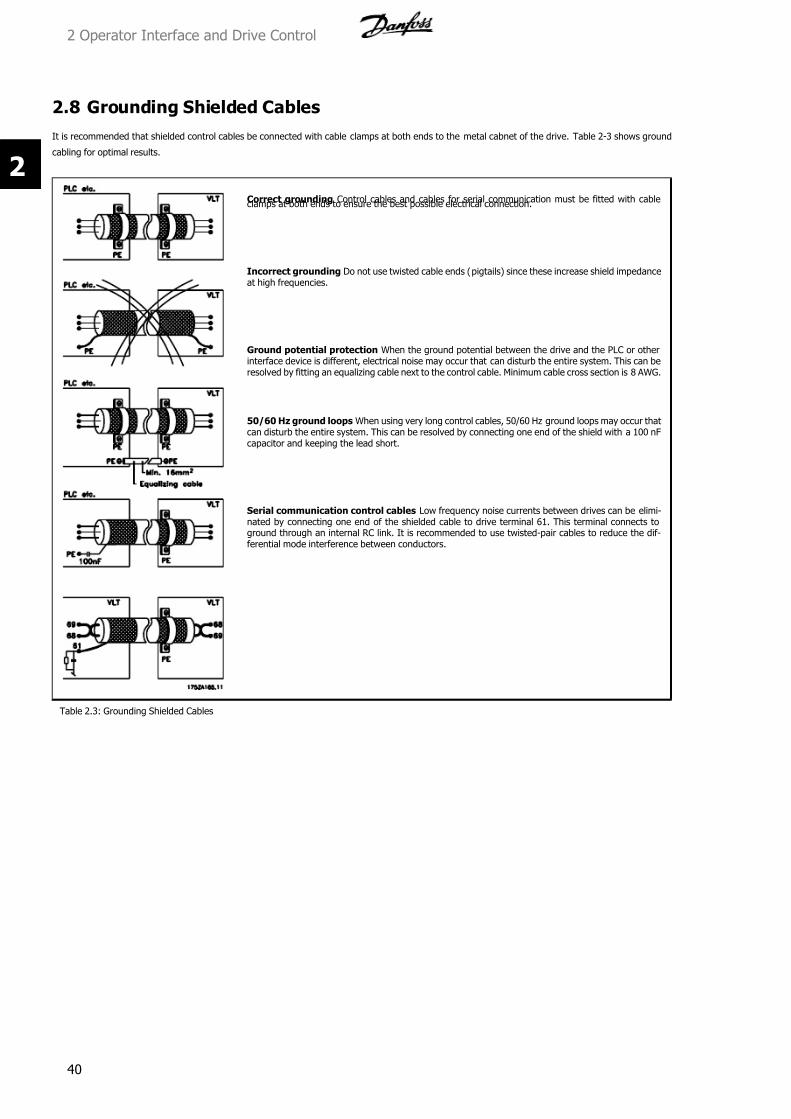
2.8 Grounding Shielded Cables
It is recommended that shielded control cables be connected with cable clamps at both ends to the metal cabnet of the drive. Table 2-3 shows ground
cabling for optimal results.
Correct grounding Control cables and cables for serial communication must be fitted with cableclamps at both ends to ensure the best possible electrical connection.
Incorrect grounding Do not use twisted cable ends (pigtails) since these increase shield impedanceat high frequencies.
Ground potential protection When the ground potential between the drive and the PLC or otherinterface device is different, electrical noise may occur that can disturb the entire system. This can beresolved by fitting an equalizing cable next to the control cable. Minimum cable cross section is 8 AWG.
50/60 Hz ground loops When using very long control cables, 50/60 Hz ground loops may occur thatcan disturb the entire system. This can be resolved by connecting one end of the shield with a 100 nFcapacitor and keeping the lead short.
Serial communication control cables Low frequency noise currents between drives can be elimi-nated by connecting one end of the shielded cable to drive terminal 61. This terminal connects toground through an internal RC link. It is recommended to use twisted-pair cables to reduce the dif-ferential mode interference between conductors.
Table 2.3: Grounding Shielded Cables
2 Operator Interface and Drive Control
40
2

7/16/2019 1. D & E Frame.pdf
http://slidepdf.com/reader/full/1-d-e-framepdf 41/197
3 Internal Drive Operation
3.1 General
This section is intended to provide an operational overview of the drive’s main assemblies and circuitry. With this information, a repair technician should
have a better understanding of the drive's operation and aid in the troubleshooting process.
3.2 Description of Operation
An adjustable frequency drive is an electronic controller that supplies a regulated amount of AC power to a three phase induction motor in order to control
the speed of the motor. By supplying variable frequency and voltage to the motor, the drive controls the motor speed, or maintains a constant speed as
the load on the motor changes. The drive can also stop and start a motor without the mechanical stress associated with a line start.
In its basic form, the drive can be divided into four main sections: rectifier, intermediate circuit, inverter, and control (see Figure 3-1).
Illustration 3.1: Control Card Logic
To provide an overview, the main drive components will be grouped into three categories consisting of the control logic section, logic to power interface,
and power section. In the sequence of operation description, these three sections will be covered in greater detail while describing how power and control
signals move throughout the drive.
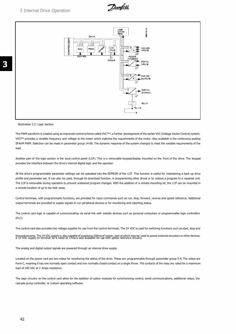
3.2.1 Logic section
The control card contains most of the logic section (see Figure 3-2). The primary logic element of the control card is a microprocessor, which supervises
and controls all functions of drive operation. In addition, separate PROMs contain the parameters to provide the user with programmable options. These
parameters are programmed to enable the drive to meet specific application requirements. This data is then stored in an EEPROM which provides security
during power-down and also allows the flexibility to change the operational characteristics of the drive.
A custom integrated circuit generates a pulse width modulation (PWM) waveform which is then sent to the interface circuitry located on the power card.
3 Internal Drive Operation
41
3
7/16/2019 1. D & E Frame.pdf
http://slidepdf.com/reader/full/1-d-e-framepdf 42/197
Illustration 3.2: Logic Section
The PWM waveform is created using an improved control scheme called VVCplus, a further development of the earlier VVC (Voltage Vector Control) system.
VVCplus provides a variable frequency and voltage to the motor which matches the requirements of the motor. Also available is the continuous pulsing
SFAVM PWM. Selection can be made in parameter group 14-00. The dynamic response of the system changes to meet the variable requirements of the
load.
Another part of the logic section is the local control panel (LCP). This is a removable keypad/display mounted on the front of the drive. The keypad
provides the interface between the drive's internal digital logic and the operator.
All the drive's programmable parameter settings can be uploaded into the EEPROM of the LCP. This function is useful for maintaining a back up drive
profile and parameter set. It can also be used, through its download function, in programming other drives or to restore a program to a repaired unit.
The LCP is removable during operation to prevent undesired program changes. With the addition of a remote mounting kit, the LCP can be mounted in
a remote location of up to ten feet away.
Control terminals, with programmable functions, are provided for input commands such as run, stop, forward, reverse and speed reference. Additional
output terminals are provided to supply signals to run peripheral devices or for monitoring and reporting status.
The control card logic is capable of communicating via serial link with outside devices such as personal computers or programmable logic controllers
(PLC).
The control card also provides two voltage supplies for use f rom the control terminals. The 24 VDC is used for switching functions such as start, stop and
forward/reverse. The 24 VDC supply is also capable of supplying 200ma of power, part of which may be used to power external encoders or other devices. A 10 VDC supply on terminal 50 is rated at 17ma is also available for use with speed reference circuitry.
The analog and digital output signals are powered through an internal drive supply.
Located on the power card are two relays for monitoring the status of the drive. These are programmable through parameter group 5-4. The relays are
Form C, meaning it has one normally open contact and one normally closed contact on a single throw. The contacts of the relay are rated for a maximum
load of 240 VAC at 2 Amps resistance.
The logic circuitry on the control card allow for the addition of option modules for synchronizing control, serial communications, additional relays, the
cascade pump controller, or custom operating software.
3 Internal Drive Operation
42
3

7/16/2019 1. D & E Frame.pdf
http://slidepdf.com/reader/full/1-d-e-framepdf 43/197
3.2.2 Logic to power interface
The logic to power interface isolates the high voltage components of the power section from the low voltage signals of the logic section. The interface
section consists of the power card and gate driver card.
Much of the fault processing for output short circuit and ground fault conditions is handled by the control card. The power card provides conditioning of
these signals. Scaling of current feedback and voltage feedback is accomplished by the control card.
The power card contains a switch mode power supply (SMPS) which provides the unit with 24 VDC, +18 VDC, –18 VDC and 5 VDC operating voltage.
The logic and interface circuitry is powered by the SMPS. The SMPS is supplied by the DC bus voltage. The drives can be purchased with an optional
secondary SMPS which is powered from a customer supplied 24 VDC source. This secondary SMPS provides power to the logic circuitry with main input
disconnected. It can keep units with communication options live on a network when the drive is not powered from the mains.
Circuitry for controlling the speed of the cooling fans is also provided on the power card.
The gate drive signals from the control card to the output transistors (IGBTs) are isolated and buffered on the gate driver card. In units that have the
dynamic brake option, the driver circuits for the brake transistors are also located on this card.
3 Internal Drive Operation
43
3
7/16/2019 1. D & E Frame.pdf
http://slidepdf.com/reader/full/1-d-e-framepdf 44/197
3.2.3 Power section
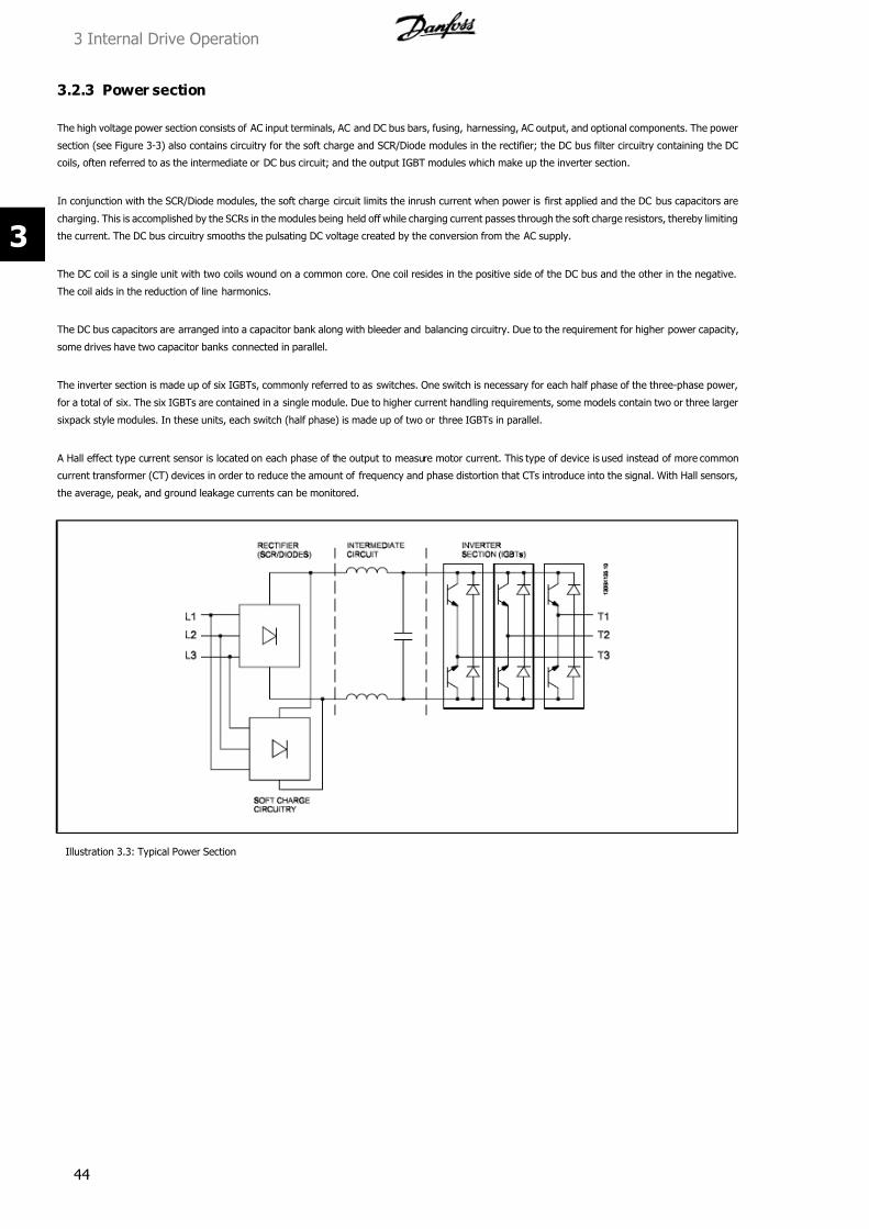
The high voltage power section consists of AC input terminals, AC and DC bus bars, fusing, harnessing, AC output, and optional components. The power
section (see Figure 3-3) also contains circuitry for the soft charge and SCR/Diode modules in the rectifier; the DC bus filter circuitry containing the DC
coils, often referred to as the intermediate or DC bus circuit; and the output IGBT modules which make up the inverter section.
In conjunction with the SCR/Diode modules, the soft charge circuit limits the inrush current when power is first applied and the DC bus capacitors are
charging. This is accomplished by the SCRs in the modules being held off while charging current passes through the soft charge resistors, thereby limiting
the current. The DC bus circuitry smooths the pulsating DC voltage created by the conversion from the AC supply.
The DC coil is a single unit with two coils wound on a common core. One coil resides in the positive side of the DC bus and the other in the negative.
The coil aids in the reduction of line harmonics.
The DC bus capacitors are arranged into a capacitor bank along with bleeder and balancing circuitry. Due to the requirement for higher power capacity,
some drives have two capacitor banks connected in parallel.
The inverter section is made up of six IGBTs, commonly referred to as switches. One switch is necessary for each half phase of the three-phase power,
for a total of six. The six IGBTs are contained in a single module. Due to higher current handling requirements, some models contain two or three larger
sixpack style modules. In these units, each switch (half phase) is made up of two or three IGBTs in parallel.
A Hall effect type current sensor is located on each phase of the output to measure motor current. This type of device is used instead of more common
current transformer (CT) devices in order to reduce the amount of frequency and phase distortion that CTs introduce into the signal. With Hall sensors,
the average, peak, and ground leakage currents can be monitored.
Illustration 3.3: Typical Power Section
3 Internal Drive Operation
44
3

7/16/2019 1. D & E Frame.pdf
http://slidepdf.com/reader/full/1-d-e-framepdf 45/197
3.3 Sequence of Operation
3.3.1 Rectifier section
When input power is first applied to the drive, it enters through the input terminals (L1, L2, L3) and on to the disconnect or/and RFI option, depending
on the unit's configuration (see Figure 3-4). If equipped with optional fuses, these fuses (FU1, FU2, FU3) limit damage caused by a short circuit in the
power section. The SCRs, in the combined SCR/Diode modules, are not gated so current can travel to the rectifier on the soft charge card. In E drive
models, the SCR and diode modules are separate. Additional fuses located on the soft charge card provide protection in the event of a short in the soft
charge or fan circuits. Three phase power is also branched off and sent to the power card. It provides the power card with a reference of the main supply
voltage and provides a supply voltage for the cooling fans.
During the charging process, the top diodes of the soft charge rectifier conduct and rectify during the positive half cycle. The diodes in the main rectifier
conduct during the negative half cycle. The DC voltage is applied to the bus capacitors through the soft charge resistor. The purpose of charging the DC
bus through this resistor is to limit the high inrush current that would otherwise be present.
Positive temperature coefficient (PTC) resistors located on the soft charge card are in series with the soft charge resistor. Frequent cycling of the input
power or the DC bus charging over an extended time can cause the PTC resistors to heat up due to the current flow. Resistance of the PTC device
increases with temperature, eventually adding enough resistance to the circuit to prevent significant current flow. This protects the soft charge resistor
from damage along with any other components that could be damaged by continuous attempts to charge the DC bus.
The low voltage power supplies are activated when the DC bus reaches approximately 50 VDC less than the alarm voltage low for the DC bus. After a
short delay, an inrush enable signal is sent from the control card to the power card SCR gating circuit. The SCRs are automatically gated when forward
biased, as a result acting similar to an uncontrolled rectifier.
When the DC bus capacitors are fully charged, the voltage on the DC bus will be equal to the peak voltage of the input AC line. Theoretically, this can be
calculated by multiplying the AC line value by 1.414 (VAC x 1.414). However, since AC ripple voltage is present on the DC bus, the actual DC value will
be closer to VAC x 1.38 under unloaded conditions and may drop to VAC x 1.32 while running under load. For example, a drive connected to a nominal
460 V line, while sitting idle, the DC bus voltage will be approximately 635 VDC (460 x 1.38).
As long as power is applied to the drive, this voltage is present in the intermediate circuit and the inverter circuit. It is also fed to the Switch Mode Power
Supply (SMPS) on the power card and is used for generating all other low voltage supplies.
3 Internal Drive Operation
45
3

7/16/2019 1. D & E Frame.pdf
http://slidepdf.com/reader/full/1-d-e-framepdf 46/197
1 3 0 B X 1 8 7 . 1 0
No RFI relay on 525 - 690V
Units. E1 units have 2 RFI
cards
PCA6
PCA12
PCA13
190843
190848
190835 190836 190836
190812
190817
190847
190815
190820
190830
190832
190833
190834
190846
190813
190812
190848
190820
202073x
20203
20203190808
ASSY 175L9471
16150
Assy 175L9472
20202
90kW=175L9426
292
ASSY 175L9421
90kW=175L9433
16005
16005
16005
90kW=16000
2379 2379 2379
10312 1031210312
10313
27653
27651
130B6865
130B6866
130B6868(Coated)
130B6885
130B6870
90kW=130B6858
130B6857130B6856 (COATED W/BRAKE)
90kW = 130B6805
FC-102/202-130B7213COATED,NO SAFESTOP
FC-102/202-130B7207COATED,WITH SAFESTOP
FC-102/202-130B7226NO SAFESTOP
FC-102/202-130B7206WITH SAFESTOP
FC-302-130B7205COATED
FC-302-130B7204
CONTROL CARD VARIANTS
130B6893130B6895-COATED
175L0109-GRAPHIC
175L0110-NUMERIC
130B0057
130B0096
IP54/NEMA12
PCA 12:
130B6872-RFI ONLY
130B6873-COATED,RFI ONLY130B6874-USEDWITH DISCSW ANDFUSES130B6875-COATED,USEDWITH DISCSW ANDFUSES
ASSY175L8314
ASSY 175L8314
LEGEND:
90kW = FC-302P90KT5
FC-202P100T4
FC-102P110T4
110kW = FC-302P110T5
FC-202P132T4
FC-102P132T4
110kW = 130B6806
110kW=130B6859
110kW=16001
110kW=175L9405
110kW=175L9427
175L9400
DCINDUCTOR
GND
L1R
MK103
RS-485
MK102
DIGITALINPUTS
MK101
ANALOG I/O
37203332292719181312
696861555453504239
1
F K 1 0 2
44
CONTROL
LCP1
PANEL
CONTROL
DISPLAY
SL2
TL3
-M+
IU
IV
+ M -
GND
U
V
W
-M
IW
+
M A I N S
IW'
IV'
IU'
S E N S O R S
C U R R E N T
T
S
R
SCRGATE DRIVER
R S T
R'
RFI OPTION
S + -
UN
UP
VN
VP
WN
WP
-
+
-
+
S'
T'
R
S
T
-SCR
+SCR
POWER CARD
SOFTCHARGE BOARD
DISC/FUSEOPTION
R S T
A
-DC
B
+DC
+DC
-DC
+
-
HF CARD
+
-
C NCNO
(DISABLEMAINS RECTIFIER)
105 106104
EXTERNALBRAKE
TEMP SWITCH
HF SWVDD
RL2+
-
AUXFAN
FANS
R ' S ' T'
R'
S'
T'
- +
-
+
DC CAP BANK ASSY
ECONOPACK+ MODULE
CURRENTSCALINGCARD
L1 L2 L 1 L 2
CCFAN
101AUX_T T
103AUX_S
100S
102X 2 X 1
L1 L1
A U X_ T
A U X_ S
A U X_ T
A U X_ S
MK103
FK102 FK103
MK100
MK105
MK107MK106
MK102
M K 1 1 1
A
-DC
C
MK400
91
92
93
94
95
98
97
96
89
88
FANO
VDD
UDC+
UDC-
M K 1 0 0
M K 1
C
B
A
BALCKT
FK1
FK2
FK3
FK4
FK5
FK6
MK1
M K 1
MK2A
C
A
B
RS+
RS-
M K 3
M K 4
NTC
-
+
GATE RESISTOR CARD
EUP1C U P1 G U P1 G L O1 EL O1
O U T
I N
MK103
NTC
MK104MK650MK450MK250 MK350
PRETEST
MK550
GATE DRIVE CARDRFI SW
RL2
VDD
MK101
MK850MK750 MK103
UMK102
MK106
MK100
M K 1 0 5
MK109
EUP2GUP2C UP 2 G LO 2 E LO 2 E UP 3GUP3CUP3 GLO3 ELO3
HF SWITCH
RFISWITCH
HF SWITCH
RFI SWITCH
18PULSENTC
FU1
FU2
FU3
PCA1
CBL2
PCA3
CBL5
PCA5
PCA8
PCA11
L1
CBANK1
SCR1 SCR2 SCR3
IGBT1
C2 C3 C4
L2
L3
L4
R1
SW1
RFI CARD
BRAKEOPTION
UDC- UDC+
M K 1
BRAKE GATE
RES CARD
G A T E
E M
C O L
BRAKE IGBT
EXT BRAKE
R+82
81 R-
RESISTOR
IGBT4
+DC
PCA9
F2
DOOR FAN1 1
3
2
3
2
CN4
GND
FAN-
FAN+
1 1
2
3
2
3
CN2
FU4
COM
FANTRANSFORMER
HEATSINK/DOOR
1
TR1
IN
OUT
3
2
CBL13
CBL14
CBL8
CBL9
CBL12
CBL15
CBL16
CBL17CBL20
CBL21
CBL23
CBL22
CBL5
CBL15
CBL24CBL9
CBL25
PCA4
CBL18 CBL19
LOADSHAREOPTION
TB3
TB1
TB2
TB4
FU5
3 6 2 5 1 4
21 3
T M P
G N D
3 2 1 6 5 4 3 2 1 3 5 4 13 11 12 9 8 1 6
10
5
8
3
6
1
GND
VPOS
SENS
DET
IU1
VNEG
VPOS
IV1
VNEG
VPOS
IW1
VNEG
10
11
12
3
4
5
6
7
8
16
14
15
12
13
9
CUR
115
3 2 1
1
2
3
3
2
1
G U P
G U N
E U P
E U N
1 5 6 1 0
E V P
G V N
G V P
1 65
V
E V N
10
E W P
G W N
G W P
1 65
W
E W N
10
G L O1
E U P 1
E L O1
U
G U P 1
4 5 8 1
MK100
VMK100
G U P 2
4E U P 2
G L O2
85E L O2
1
WMK100
G U P 3
4E U P 3
G L O 3
85E L O 3
1
T M P +
T M P -
NTC
1 2 3
N T C 1
N T C 2
NTC
1 2 3
E U N
G U N
1 32
GUN GUP
E U P
2
G U P
1 3
GVN
E V N
2
G V N
1
GVP
E V P
G V P
3 1 2 3
GWN
E W N
2
G W N
1
GWP
E W P
G W P
3 1 2 3
BRK
B R N
G B P
21 3
G2
E1/C24
6
1
1
5
6 B R K
B R K
BRC
BRN
GBP
E2
CN3
5
4
3
2
1
GRN
BLK
BLK
WHT
GRN4
C1
BLK
BLK
6 6
5HEATSINK
FANCAPACITOR
FANHEATSINK
HSFANASSEMBLY
ORN
BLU
WHT
3
2
1
F1
NCNOC
1 2 3
MK112
RELAY1
44
1
M K 1 1 0FC-X02
CARD
RELAY2
4 5 6
C N O N C
M K 1 0 4
TEST CONNECTOR
1
30
NEMA 1,
UNITS ONLY.
FAN+
FAN-
F4
F5
11
2
3
2
3
FAN-
FAN+
2
3
1
2
3
1TOPFANUSED ONCHASSIS ANDIP00UNITSONLY.
CBL1
CN5
CN6
3x190831
27Ohms
TOPFANUSED ONCHASSIS ANDIP00UNITSONLY.
NEMA 12,IP 21,IP 54
Illustration 3.4: Rectifier circuit
3 Internal Drive Operation
46
3

7/16/2019 1. D & E Frame.pdf
http://slidepdf.com/reader/full/1-d-e-framepdf 47/197
3.3.2 Intermediate section
Following the rectifier section, voltage passes to the intermediate section. (see Figure 3-5). This rectified voltage is smoothed by an LC filter circuit
consisting of the DC bus inductor and the DC bus capacitor bank.
The DC bus inductor provides series impedance to changing current. This aids the filtering process while reducing harmonic distortion to the input AC
current waveform normally inherent in rectifier circuits.
The DC capacitor bank assembly consists of up to eight capacitors arranged in series/parallel configuration. Higher power units have two capacitor banks
assemblies. Also contained within the assembly is the bleeder/balance circuitry. This circuitry maintains equal voltage drops across each capacitor and
provides a current path for discharging the capacitors once power has been removed from the drive.
Also located in the intermediate section is the high frequency (HF) filter card. It contains a high frequency filter circuit to reduce naturally occurring
currents in the HF range to prevent interference with other sensitive equipment in the area. The circuit, as with other RFI filter circuitry, can be sensitive
to unbalanced phase-to-ground voltages in the three-phase AC input line. This can occasionally result in nuisance overvoltage alarms. For this reason,
the high frequency filter card on 380 - 500 V range drives, contains a set of relay contacts in the ground connection of the filter capacitors. The relay is
tied into the RFI/HF switch, which can be switched off or on in parameter 14-50. This disconnects the ground references to all filters should unbalanced
phase-to-ground voltages create nuisance overvoltage conditions.
For 525-690 V drives, there are no relay contacts that disconnect the ground.
3 Internal Drive Operation
47
3

7/16/2019 1. D & E Frame.pdf
http://slidepdf.com/reader/full/1-d-e-framepdf 48/197
1 3 0 B X 1 8 8 . 1 0
No RFI relay on 525 - 690V
units
PCA6
PCA12
PCA13
190843
190848
190835 190836 190836
190812
190817
190847
190815
190820
190830
190832
190833
190834
190846
190813
190812
190848
190820
202073x
20203
20203190808
ASSY175L9471
16150
Assy 175L9472
20202
90kW=175L9426
292
ASSY175L9421
90kW=175L9433
16005
16005
16005
90kW=16000
2379 2379 2379
10312 1031210312
10313
27653
27651
130B6865
130B6866
130B6868(Coated)
130B6885
130B6870
90kW=130B6858
130B6857
130B6856 (COATED W/BRAKE)
90kW = 130B6805
FC-102/202-130B7213COATED,NOSAFE STOP
FC-102/202-130B7207COATED,WITHSAFE STOP
FC-102/202-130B7226NO SAFESTOP
FC-102/202-130B7206WITHSAFE STOP
FC-302-130B7205COATED
FC-302-130B7204
CONTROL CARD VARIANTS
130B6893
130B6895-COATED
175L0109-GRAPHIC
175L0110-NUMERIC
130B0057
130B0096
IP54/NEMA12
PCA 12:
130B6872-RFIONLY
130B6873-COATED,RFIONLY
130B6874-USEDWITH DISCSW ANDFUSES130B6875-COATED,USEDWITHDISCSWANDFUSES
ASSY175L8314
ASSY175L8314
LEGEND:
90kW=FC-302P90KT5
FC-202P100T4
FC-102P110T4
110kW=FC-302P110T5
FC-202P132T4
FC-102P132T4
110kW = 130B6806
110kW=130B6859
110kW=16001
110kW=175L9405
110kW=175L9427
175L9400
DCINDUCTOR
GND
L1R
MK103
RS-485
MK102
DIGITAL INPUTS
MK101
ANALOG I/O
37203332292719181312
696861555453504239
1
F K 1 0 2
44
CONTROL
LCP1
PANEL
CONTROL
DISPLAY
SL2
TL3
-M+
IU
IV
+ M -
GND
U
V
W
-M
IW
+
M A I N S
IW'
IV'
IU'
S E N S O R S
C U R R E N T
T
S
R
SCRGATEDRIVER
R S T
R'
RFIOPTION
S + -
UN
UP
VN
VP
WN
WP-
+
-
+
S'
T'
R
S
T
-SCR
+SCR
POWER CARD
SOFTCHARGE BOARD
DISC/FUSEOPTION
R S T
A
-DC
B
+DC
+DC
-DC
+
-
HF CARD
+
-
C NCNO
(DISABLEMAINS RECTIFIER)
105 106104
EXTERNALBRAKE
TEMPSWITCH
HF SWVDD
RL2+
-
AUX FAN
FANS
R ' S ' T '
R'
S'
T'
- +
-
+
DC CAP BANK ASSY
ECONOPACK+MODULE
CURRENTSCALING
CARD
L1 L2 L1 L2
CCFAN
101AUX_T T
103AUX_S
100S
102 X 2 X 1
L1 L1 A U X_
T
A U X_
S
A U X_
T
A U X_
S
MK103
FK102 FK103
MK100
MK105
MK107MK106
MK102
M K 1 1 1
A
-DC
C
MK400
91
92
93
94
95
98
97
96
89
88
FANO
VDD
UDC+
UDC-
M K 1 0 0
M K 1
C
B
A
BAL CKT
FK1
FK2
FK3
FK4
FK5
FK6
MK1
M K 1
MK2A
C
A
B
RS+
RS-
M K 3
M K 4
NTC
-
+
GATE RESISTOR CARD
EUP1C U P 1 G U P1 G L O 1 E LO 1
O U T
I N
MK103
NTC
MK104MK650MK450MK250 MK350
PRETEST
MK550
GATE DRIVE CARDRFI SW
RL2
VDD
MK101
MK850MK750 MK103
UMK102
MK106
MK100
M K 1 0 5
MK109
EUP2GUP2C U P2 G L O2 E L O2 E U P3GUP3C U P3 G L O3 EL O 3
HF SWITCH
RFISWITCH
HFSWITCH
RFISWITCH
18 PULSE NTC
FU1
FU2
FU3
PCA1
CBL2
PCA3
CBL5
PCA5
PCA8
PCA11
L1
CBANK1
SCR1 SCR2 SCR3
IGBT1
C2 C3 C4
L2
L3
L4
R1
SW1
RFI CARD
BRAKEOPTION
UDC- UDC+
M K 1
BRAKE GATE
RES CARD
G A T E
E M
C O L
BRAKE IGBT
EXTBRAKE
R+82
81 R-
RESISTOR
IGBT4
+DC
PCA9
F2
DOORFAN1 1
3
2
3
2
CN4
GND
FAN-
FAN+
1 1
2
3
2
3
CN2
FU4
COM
FAN TRANSFORMERHEATSINK/DOOR
1
TR1
IN
OUT
3
2
CBL13
CBL14
CBL8
CBL9
CBL12
CBL15
CBL16
CBL17CBL20
CBL21
CBL23
CBL22
CBL5
CBL15
CBL24CBL9
CBL25
PCA4
CBL18 CBL19
LOAD SHARE OPTION
TB3
TB1
TB2
TB4
FU5
3 6 2 5 1 4
21 3
T M P
G N D
3 2 1 6 5 4 3 2 1 3 5 4 13 11 12 9 8 1 6
10
5
8
3
6
1
GND
VPOS
SENS
DET
IU1
VNEG
VPOS
IV1
VNEG
VPOS
IW1
VNEG
1011
123
4
5
6
7
816
14
15
1213
9
CUR
115
3 2 1
1
2
3
3
2
1
G U P
G U N E U P E U N
1 5 6 1 0
E V P
G V N
G V P
1 65
V
E V N
10
E W P
G W N
G W P
1 65
W
E W N
10
G L O1
E U P 1
E L O1
U
G U P 1
4 5 8 1
MK100
VMK100
G U P 2
4E U P 2
G L O2
85E L O2
1
WMK100
G U P 3
4E U P 3
G L O 3
85E L O 3
1
T M P +
T M P -
NTC
1 2 3
N T C 1
N T C 2
NTC
1 2 3
E U N
G U N
1 32
G U N G U P
E U P
2
G U P
1 3
GVN
E V N
2
G V N
1
GVP
E V P
G V P
3 1 2 3
GWN
E W N
2
G W N
1
GWP
E W P
G W P
3 1 2 3
BRK
B R N
G B P
21 3
G2
E1/C2
4
6
1
1
5
6 B R K
B R K
BRC
BRN
GBP
E2
CN3
5
4
3
2
1
GRN
BLK
BLK
WHT
GRN4
C1
BLK
BLK
6 6
5 HEATSINK
FANCAPACITOR
FANHEATSINK
HS FAN ASSEMBLY
ORN
BLU
WHT
3
2
1
F1
NCNOC
1 2 3
MK112
RELAY1
44
1
M K 1 1 0
FC-X02
CARD
RELAY2
4 5 6
C NO NC
M K 1 0 4
TESTCONNECTOR
1
30
NEMA 1,
UNITSONLY.
FAN+
FAN-
F4
F5
11
2
3
2
3
FAN-
FAN+
2
3
1
2
3
1TOPFANUSED ONCHASSIS ANDIP00 UNITSONLY.
CBL1
CN5
CN6
3x190831
27Ohms
TOPFANUSED ONCHASSIS ANDIP00 UNITSONLY.
NEMA12,IP 21,IP 54
Illustration 3.5: Intermediate section
3 Internal Drive Operation
48
3

7/16/2019 1. D & E Frame.pdf
http://slidepdf.com/reader/full/1-d-e-framepdf 49/197
3.3.3 Inverter section
In the inverter section (see Figure 3-7), gate signals are delivered from the control card, through the power card and gate drive card to the gates of the
IGBTs. The series connection of each set of IGBTs is delivered to the output, first passing through the current sensors.
Once a run command and speed reference are present, the IGBTs begin switching to create the output waveform, as shown in Figure 3-6. Looking at
the phase-to-phase voltage waveform with an oscilloscope, it can be seen that the Pulse Width Modulation (PWM) principal creates a series of pulses
which vary in width. Basically, the pulses are narrower as zero crossing is neared and wider the farther from zero crossing. The width is controlled by the
pulse duration of applied DC voltage. Although the voltage waveform is a consistent amplitude, the inductance within the motor windings will serve to
average the voltage delivered and so, as the pulse width of the waveform varies, the average voltage seen by the motor varies as well. This then equates
to the resultant current waveform which takes on the sine wave shape that we expect to see in an AC system. The frequency of the waveform is then
determined by the rate at which the pulses occur. By employing a sophisticated control scheme, the drive is capable of delivering a current waveform
that nearly replicates a true AC sine wave.
This waveform, as generated by the Danfoss VVCplus PWM principle at the control card, provides optimal performance and minimal losses in the motor.
Hall effect current sensors monitor the output current and deliver proportional signals to the power card where they are buffered and delivered to the
control card. These current signals are used by the control card logic to determine proper waveform compensations based on load conditions. They further
serve to detect overcurrent conditions, including ground faults and phase-to-phase shorts on the output.
During normal operation, the power card and control card are monitoring various functions within the drive. The current sensors provide current feedback
information. The DC bus voltage and AC line voltage are monitored as well as the voltage delivered to the motor. A thermal sensor mounted inside one
of IGBT modules provides heatsink temperature feedback.
1 3 0 B X 1 3 6 . 1 0
Illustration 3.6: Output Voltage and Current Waveforms
3 Internal Drive Operation
49
3
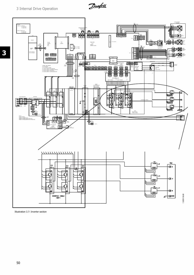
7/16/2019 1. D & E Frame.pdf
http://slidepdf.com/reader/full/1-d-e-framepdf 50/197
1 3 0 B X 1 8 6 . 1 0
PCA6
PCA12
PCA13
190843
190848
190835 190836 190836
190812
190817
190847
190815
190820
190830
190832
190833
190834
190846
190813
190812
190848
190820
202073x
20203
20203190808
ASSY175L9471
16150
Assy 175L9472
20202
90kW=175L9426
292
ASSY175L9421
90kW=175L9433
16005
16005
16005
90kW=16000
2379 2379 2379
10312 1031210312
10313
27653
27651
130B6865
130B6866
130B6868(Coated)
130B6885
130B6870
90kW=130B6858
130B6857130B6856 (COATED W/BRAKE)
90kW = 130B6805
FC-102/202-130B7213 COATED,NO SAFESTOP
FC-102/202-130B7207 COATED,WITH SAFESTOP
FC-102/202-130B7226 NO SAFESTOP
FC-102/202-130B7206 WITH SAFESTOP
FC-302-130B7205 COATED
FC-302-130B7204
CONTROL CARD VARIANTS
130B6893130B6895-COATED
175L0109-GRAPHIC
175L0110-NUMERIC
130B0057
130B0096
IP54/NEMA12
PCA 12:
130B6872-RFI ONLY
130B6873-COATED,RFI ONLY130B6874-USEDWITH DISCSW ANDFUSES130B6875-COATED,USEDWITH DISC SW ANDFUSES
ASSY175L8314
ASSY175L8314
LEGEND:
90kW=FC-302P90KT5
FC-202P100T4
FC-102P110T4
110kW=FC-302P110T5
FC-202P132T4
FC-102P132T4
110kW = 130B6806
110kW=130B6859
110kW=16001
110kW=175L9405
110kW=175L9427
175L9400
DC INDUCTOR
GND
L1R
MK103
RS-485
MK102
DIGITALINPUTS
MK101
ANALOG I/O
37203332292719181312
696861555453504239
1
F K 1 0 2
44
CONTROL
LCP1
PANELCONTROL
DISPLAY
SL2
TL3
-M+
IU
IV
+ M -
GND
U
V
W
-M
IW
+
M A I N S
IW'
IV'
IU'
S E N S O R S
C U R R E N T
T
S
R
SCR
GATE DRIVER
R S T
R'
RFI OPTION
S + -
UN
UP
VN
VP
WN
WP
-
+
-
+
S'
T'
R
S
T
-SCR
+SCR
POWER CARD
SOFTCHARGE BOARD
DISC/FUSEOPTION
R S T
A
-DC
B
+DC
+DC
-DC
+
-
HF CARD
+
-
C NCNO
(DISABLE MAINS RECTIFIER)
105 106104
EXTERNALBRAKE TEMP SWITCH
HF SWVDD
RL2+
-
AUXFAN
FANS
R ' S ' T'
R'
S'
T'
- +
-
+
DC CAP BANK ASSY
ECONOPACK+ MODULE
CURRENT
SCALINGCARD
L1 L2 L1 L2
CC FAN
101AUX_T T
103AUX_S
100
S
102X 2 X 1
L1 L1
A U X_
T
A U X_
S
A U X_
T
A U X_
S
MK103
FK102 FK103
MK100
MK105
MK107MK106
MK102
M K 1 1 1
A
-DC
C
MK400
91
92
93
94
95
98
97
96
89
88
FANO
VDD
UDC+
UDC-
M K 1 0 0
M K 1
C
B
A
BALCKT
FK1
FK2
FK3
FK4
FK5
FK6
MK1
M K 1
MK2A
C
A
B
RS+
RS-
M K 3
M K 4
NTC
-
+
GATE RESISTOR CARD
EUP1C UP1 GUP1 GL O 1 E L O1
O U T
I N
MK103
NTC
MK104MK650MK450MK250 MK350
PRE TEST
MK550
GATE DRIVE CARDRFI SW
RL2
VDD
MK101
MK850MK750 MK103
UMK102
MK106
MK100
M K 1 0 5
MK109
EUP2GUP2CUP2 GLO2 ELO2 EUP3GUP3CUP3 GLO3 ELO3
HFSWITCH
RFISWITCH
HFSWITCH
RFISWITCH
18PULSENTC
FU1
FU2
FU3
PCA1
CBL2
PCA3
CBL5
PCA5
PCA8
PCA11
L1
CBANK1
SCR1 SCR2 SCR3
IGBT1
C2 C3 C4
L2
L3
L4
R1
SW1
RFI CARD
BRAKEOPTION
UDC- UDC+
M K 1
BRAKE GATE
RES CARD
G A T E
E M
C O L
BRAKE IGBT
EXT BRAKE
R+82
81 R-
RESISTOR
IGBT4
+DC
PCA9
F2
DOOR FAN1 1
3
2
3
2
CN4
GND
FAN-
FAN+
1 1
2
3
2
3
CN2
FU4
COM
FAN TRANSFORMERHEATSINK/DOOR
1
TR1
IN
OUT
3
2
CBL13
CBL14
CBL8
CBL9
CBL12
CBL15
CBL16
CBL17CBL20
CBL21
CBL23
CBL22
CBL5
CBL15
CBL24CBL9
CBL25
PCA4
CBL18 CBL19
LOADSHAREOPTION
TB3
TB1
TB2
TB4
FU5
3 6 2 5 1 4
21 3
T M P
G N D
3 2 1 6 5 4 3 2 1 3 5 4 1 3 1 1 12 9 8 1 6
10
5
8
3
6
1
GND
VPOS
SENS
DET
IU1
VNEG
VPOS
IV1
VNEG
VPOS
IW1
VNEG
1011
12
3
4
5
6
7
8
16
1415
12
13
9
CUR
115
3 2 1
1
2
3
3
2
1
G U P
G U N
E U P
E U N
1 5 6 10
E V P
G V N
G V P
1 65
V
E V N
10
E W P
G W N
G W P
1 65
W
E W N
10
G L O1
E U P 1
E L O1
U
G U P 1
4 5 8 1
MK100
VMK100
G U P 2
4E U P 2
G L O2
85E L O2
1
WMK100
G U P 3
4E U P 3
G L O 3
85E L O 3
1
T M P +
T M P -
NTC
1 2 3
N T C 1
N T C 2
NTC
1 2 3
E U N
G U N
1 32
G UN G UP
E U P
2
G U P
1 3
GVN
E V N
2
G V N
1
GVP
E V P
G V P
3 1 2 3
GWN
E W N
2
G W N
1
GWP
E W P
G W P
3 1 2 3
BRK
B R N
G B P
21 3
G2
E1/C24
6
1
1
5
6 B R K
B R K
BRC
BRN
GBP
E2
CN3
5
4
3
2
1
GRN
BLK
BLK
WHT
GRN4
C1
BLK
BLK
6 6
5HEATSINK
FANCAPACITOR
FANHEATSINK
HS FAN ASSEMBLY
ORN
BLU
WHT
3
2
1
F1
NCNOC
1 2 3
MK112
RELAY1
44
1
M K 1 1 0FC-X02
CARD
RELAY2
4 5 6
C N O N C
M K 1 0 4
TEST CONNECTOR
1
30
NEMA 1,
UNITS ONLY.
FAN+
FAN-
F4
F5
11
2
3
2
3
FAN-
FAN+
2
3
1
2
3
1TOP FANUSEDONCHASSIS ANDIP00UNITSONLY.
CBL1
CN5
CN6
3x190831
27Ohms
TOP FANUSEDONCHASSIS ANDIP00UNITSONLY.
NEMA 12,IP21,IP 54
Illustration 3.7: Inverter section
3 Internal Drive Operation
50
3

7/16/2019 1. D & E Frame.pdf
http://slidepdf.com/reader/full/1-d-e-framepdf 51/197
3.3.4 Brake option
For drives equipped with the dynamic brake option, a brake IGBT along with terminals 81(R-) and 82(R+) is included for connecting an external brake
resistor.
The function of the brake IGBT (see Figure 3-8) is to limit the voltage in the intermediate circuit, whenever the maximum voltage limit is exceeded. It
does this by switching the externally mounted resistor across the DC bus to remove excess DC voltage present on the bus capacitors. Excess DC bus
voltage is generally a result of an overhauling load causing regenerative energy to be returned to the DC bus. This occurs, for example, when the load
drives the motor causing the voltage to return to the DC bus circuit.
Placing the brake resistor externally has the advantages of selecting the resistor based on application need, dissipating the energy outside of the control
panel, and protecting the drive from overheating if the brake resistor is overloaded.
The Brake IGBT gate signal originates on the control card and is delivered to the brake IGBT via the power card and gate drive card. Additionally, the
power and control cards monitor the brake IGBT and brake resistor connection for short circuits and overloads.
3 Internal Drive Operation
51
3
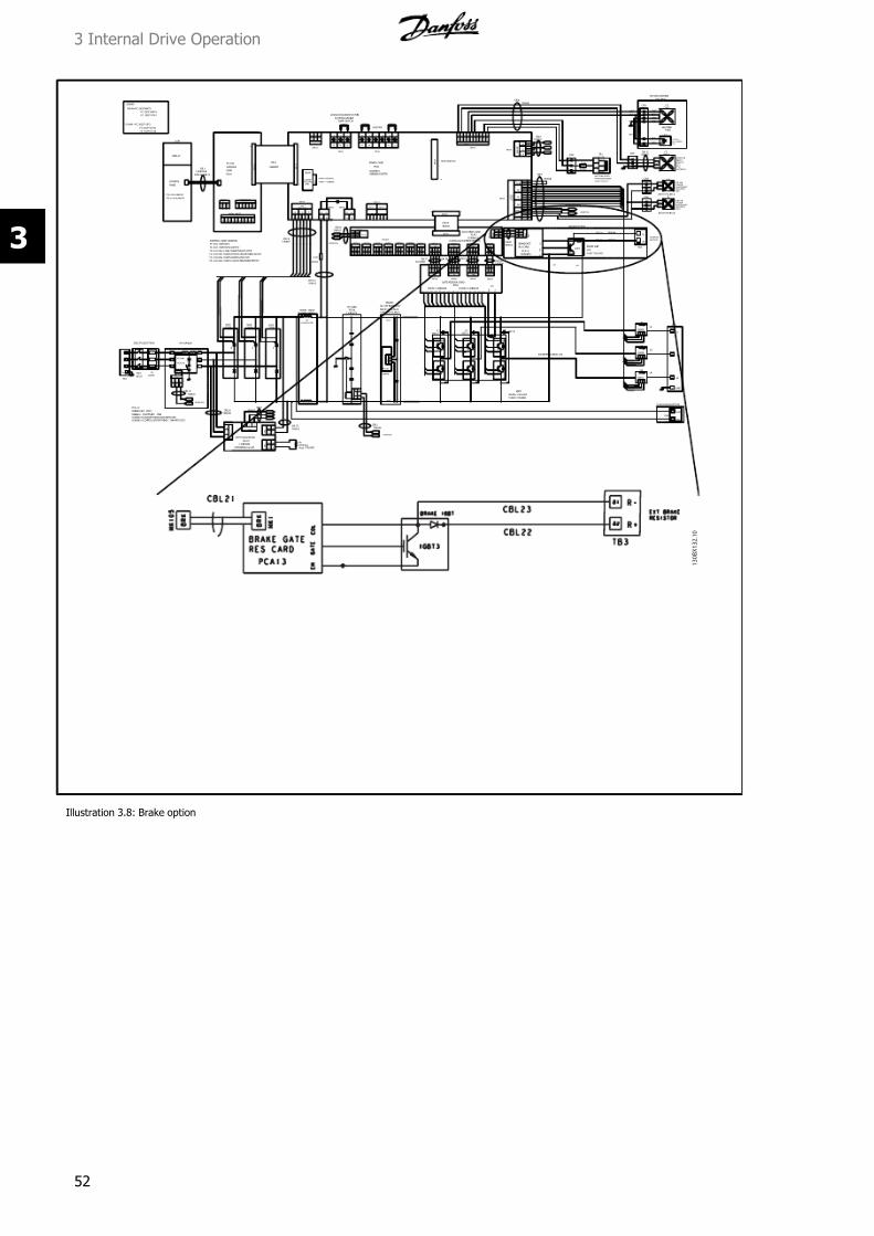
7/16/2019 1. D & E Frame.pdf
http://slidepdf.com/reader/full/1-d-e-framepdf 52/197
1 3 0 B X 1 3 2 . 1 0
PCA6
PCA12
PCA13
190843
190848
190835 190836 190836
190812
190817
190847
190815
190820
190830
190832
190833
190834
190846
190813
190812
190848
190820
202073x
20203
20203190808
ASSY175L9471
16150
Assy 175L9472
20202
90kW=175L9426
292
ASSY175L9421
90kW=175L9433
16005
16005
16005
90kW=16000
2379 2379 2379
10312 1031210312
10313
27653
27651
130B6865
130B6866
130B6868(Coated)
130B6885
130B6870
90kW=130B6858
130B6857130B6856(COATEDW/BRAKE)
90kW = 130B6805
FC-102/202-130B7213COATED,NO SAFESTOP
FC-102/202-130B7207COATED,WITH SAFESTOP
FC-102/202-130B7226NO SAFESTOP
FC-102/202-130B7206WITH SAFESTOP
FC-302-130B7205COATED
FC-302-130B7204CONTROL CARD VARIANTS
130B6893130B6895-COATED
175L0109-GRAPHIC
175L0110-NUMERIC
130B0057
130B0096
IP54/NEMA12
PCA 12:
130B6872-RFI ONLY
130B6873- COATED,RFI ONLY130B6874-USEDWITH DISCSW ANDFUSES130B6875-COATED,USEDWITH DISC SW ANDFUSES
ASSY175L8314
ASSY175L8314
LEGEND:
90kW=FC-302P90KT5
FC-202P100T4
FC-102P110T4
110kW = FC-302P110T5
FC-202P132T4
FC-102P132T4
110kW = 130B6806
110kW=130B6859
110kW=16001
110kW=175L9405
110kW=175L9427
175L9400
DCINDUCTOR
GND
L1
R
MK103
RS-485
MK102
DIGITAL INPUTS
MK101
ANALOGI/O
37203332292719181312
696861555453504239
1
F K 1 0 2
44
CONTROL
LCP1
PANEL
CONTROL
DISPLAY
S
L2
T
L3
-M+
IU
IV
+ M -
GND
U
V
W
-M
IW
+
M A I N S
IW'
IV'
IU'
S E N S O R S
C U R R E N T
T
S
R
SCRGATEDRIVER
R S T
R'
RFI OPTION
S + -
UN
UP
VN
VP
WN
WP-
+
-
+
S'
T'
R
S
T
-SCR
+SCR
POWER CARD
SOFTCHARGE BOARD
DISC/FUSEOPTION
R S T
A
-DC
B
+DC
+DC
-DC
+
-
HF CARD
+
-
C NCNO
(DISABLEMAINSRECTIFIER)
105 106104
EXTERNALBRAKE TEMP SWITCH
HFSWVDD
RL2+
-
AUX FAN
FANS
R ' S ' T'
R'
S'
T'
- +
-
+
DC CAP BANK ASSY
ECONOPACK+MOD ULE
CURRENTSCALINGCARD
L 1 L 2 L 1 L 2
CC FAN
101AUX_T T
103AUX_S
100
S
102X 2 X 1
L1 L1
A U X_ T
A U X_ S
A U X_ T
A U X_ S
MK103
FK102 FK103
MK100
MK105
MK107MK106
MK102
M K 1 1 1
A
-DC
C
MK400
91
92
93
94
95
98
97
96
89
88
FANO
VDD
UDC+
UDC-
M K 1 0 0
M K 1
C
B
A
BALCKT
FK1
FK2
FK3
FK4
FK5
FK6
MK1
M K
1
MK2A
C
A
B
RS+
RS-
M K 3
M K 4
NTC
-
+
GATE RESISTOR CARD
EUP1CUP1 GUP1 GLO1 ELO1
O U T
I N
MK103
NTC
MK104MK650MK450MK250 MK350
PRETEST
MK550
GATE DRIVE CARDRFISW
RL2
VDD
MK101
MK850MK750 MK103
UMK102
MK106
MK100
M K 1 0 5
MK109
EUP2GUP2CUP2 GLO2 ELO2 EUP3GUP3CUP3 GLO3 ELO3
HF SWITCH
RFI SWITCH
HFSWITCH
RFI SWITCH
18PULSENTC
FU1
FU2
FU3
PCA1
CBL2
PCA3
CBL5
PCA5
PCA8
PCA11
L1
CBANK1
SCR1 SCR2 SCR3
IGBT1
C2 C3 C4
L2
L3
L4
R1
SW1
RFI CARD
BRAKEOPTION
UDC- UDC+
M K 1
BRAKEGATE
RES CARD
G A T E
E M
C O L
BRAKE IGBT
EXT BRAKE
R+82
81 R-
RESISTOR
IGBT4
+DC
PCA9
F2
DOOR FAN1 1
3
2
3
2
CN4
GND
FAN-
FAN+
1 1
2
3
2
3
CN2
FU4
COM
FANTRANSFORMER
HEATSINK/DOOR
1
TR1
IN
OUT
3
2
CBL13
CBL14
CBL8
CBL9
CBL12
CBL15
CBL16
CBL17CBL20
CBL21
CBL23
CBL22
CBL5
CBL15
CBL24CBL9
CBL25
PCA4
CBL18 CBL19
LOADSHAREOPTION
TB3
TB1
TB2
TB4
FU5
3 6 2 5 1 4
21 3
T M P
G N D
3 2 1 6 5 4 3 2 1 3 5 4 13 11 12 9 8 1 6
10
5
8
3
6
1
GND
VPOS
SENS
DET
IU1
VNEG
VPOS
IV1
VNEG
VPOS
IW1
VNEG
1011
123
4
5
6
7
816
1415
1213
9
CUR
115
3 2 1
1
2
3
3
2
1
G U P
G U N
E U P
E U N
1 5 6 10
E V P
G V N
G V P
1 65
V
E V N
10
E W P
G W N
G W P
1 65
W
E W N
10
G L O1
E U P 1
E L O1
U
G U P 1
4 5 8 1
MK100
VMK100
G U P 2
4E U P 2
G L O2
85E L O2
1
WMK100
G U P 3
4E U P 3
G L O 3
85E L O 3
1
T M P +
T M P -
NTC
1 2 3
N T C 1
N T C 2
NTC
1 2 3
E U N
G U N
1 32
GUN GUP
E U P
2
G U P
1 3
GVN
E V N
2
G V N
1
GVP
E V P
G V P
3 1 2 3
GWN
E W N
2
G W N
1
GWP
E W P
G W P
3 1 2 3
BRK
B R N
G B P
21 3
G2
E1/C24
6
1
1
5
6 B R K
B R K
BRC
BRN
GBP
E2
CN3
5
4
3
2
1
GRN
BLK
BLK
WHT
GRN4
C1
BLK
BLK
6 6
5HEATSINK
FAN CAPACITOR
FANHEATSINK
HSFANASSEMBLY
ORN
BLU
WHT
3
2
1
F1
NCNOC
1 2 3
MK112
RELAY 1
44
1
M K 1 1 0FC-X02
CARD
RELAY2
4 5 6
C N O N C
M K 1 0 4
TESTCONNECTOR
1
30
NEMA1,
UNITS ONLY.
FAN+
FAN-
F4
F5
11
2
3
2
3
FAN-
FAN+
2
3
1
2
3
1TOP FANUSEDONCHASSIS ANDIP00UNITSONLY.
CBL1
CN5
CN6
3x190831
27Ohms
TOP FANUSEDONCHASSIS ANDIP00UNITSONLY.
NEMA 12,IP 21,IP54
Illustration 3.8: Brake option
3 Internal Drive Operation
52
3

7/16/2019 1. D & E Frame.pdf
http://slidepdf.com/reader/full/1-d-e-framepdf 53/197
3.3.5 Cooling fans
All drives in this size range are equipped with cooling fans to provide airflow along the heatsink. Units in NEMA 1 (IP21) and NEMA 12 (IP54) enclosures
have a fan mounted in the enclosure door to provide additional airflow to the unit. Chassis (IP00) enclosures have a fan or fans mounted to the top of
the unit for additional cooling. Some drives in this size range have a small 24 VDC fan mounted on the input plate. This fan is only mounted on E-frame
size units equipped with both an RFI filter and mains fuses. The fan provides air flow around the main fuses. The fan operates anytime the drive is
powered.
All fans are powered by line voltage which is stepped down by an autotransformer and regulated to 200 or 230 VAC by circuitry provided on the power
card. On/off and high/low speed control of the fans is provided to reduce overall acoustical noise and extend the l ife of the fans.
Fans are activated by the following causes:
60% of nominal current exceeded
Specific heatsink temperature exceeded (power size dependent)
DC hold active
DC brake active
Pre-magnetization of the motor
Automatic motor adaptation in progress
Regardless of the heatsink temperature, the fans are started shortly after main input power is applied to the drive.
Once fans are started, they will run for minimum 10 minutes.
3.3.6 Fan speed control
The cooling fans are controlled with sensor feedback which regulates fan operation and speed control as described below.
1. IGBT thermal sensor measured temperature. The fan can be off, low speed, or high speed based on this temperature.
IGBT Thermal Sensor D Frame Units E Frame UnitsFan Turn On Low Speed 45°C 45°CFan Low Speed to High Speed 50°C 50°CFan High Speed to Low Speed 40°C 40°CFan Turn Off from Low Speed 30°C 30°C
Table 3.1: IGBT Thermal Sensor
2. Power card ambient temperature sensor measured temperature. The fan can be off or high speed based on this temperature.
Power Card Ambient D Frame Units E Frame UnitsFan turn on to High Speed 35°C 45°CFan turn off from High Speed 30°C 40°CFan turn on to High Speed <10°C <10°C
Table 3.2: Power Card Ambient Temperature Sensor
2. Control card thermal sensor measured temperature. The fan can be off or low speed based on this temperature.
Control Card Ambient D Frame Units E Frame UnitsFan turn on to Low Speed 55°C 55°CFan turn off from Low Speed 45°C 45°C
Table 3.3: Control Card Thermal Sensor
2. Output current value. If the output current is greater than 60% of rated current, the fan will turn on low speed.
3 Internal Drive Operation
53
3
7/16/2019 1. D & E Frame.pdf
http://slidepdf.com/reader/full/1-d-e-framepdf 54/197
3.3.7 Load Sharing
Units with the built-in load sharing option contain terminals 89 (+) DC and 88 (-) DC. Within the drive, these terminals connect to the DC bus in front of
the DC link reactor and bus capacitors.
The use of the load sharing terminals can take on two different configurations.
In one method, the terminals are used to tie the DC bus circuits of multiple drives together. This allows for the possibility of one drive that is in a
regenerative mode to share its excess bus voltage with another drive that is in the motoring mode. When applied correctly, this can reduce the need for
external dynamic brake resistors while also saving energy. In theory, the number of drives that can be connected in this way is infinite, however, the
drives must be of the same voltage rating. In addition, depending on the size and number of drives, it may be necessary to install DC reactors and DC
fuses in the DC link connections and AC reactors on the mains. Attempting such a configuration requires specific considerations and should not be
attempted without first consulting Danfoss Application Engineering.
In the second method, the drive is powered exclusively from a DC source. This is a bit more complicated. First, a DC source is required. Second, a means
to soft charge the DC bus at power up is required. Last, a line voltage source is required to power the fans within the drive. Again such a configuration
should not be attempted with out first consulting Danfoss Application Engineering.
3.3.8 Specific card connections
Connector FK102, terminals 104, 105 and 106 located on the power card, provide for the connection of an external temperature switch. The input could
be used to monitor the temperature of an external brake resistor. Two input configurations are possible. A normally closed switch may be connected
between terminals 104 and 106 or a normally open switch between terminals 104 and 105. Should the input change states, the drive would trip on an
Alarm 29, Overtemperature. The input SCRs would also be disabled to prevent further energy from being supplied to the DC bus. If no such input is used,
or the normally open configuration is selected, a jumper must be installed between terminals 104 and 106.
Connector FK103, terminals 100, 101, 102, and 103 located on the power card, provide for the connection of line voltage to allow powering the AC cooling
fans from an external source. This is required when the drive is used in a load sharing application where no AC power is provided to the main input
terminals. To make use of this provision, the jumpers would be removed from terminals 100 and 102, 101 and 103. The auxiliary line voltage power
supply would be connected to terminals 100 and 101.
The power card MK112, terminals 1, 2, and 3, and 4, 5, and 6 provide access to 2 auxiliary relays. These are form C sets of contacts, meaning one
normally open and one normally closed contact on a single throw. The contacts are rated for a maximum of 240 VAC, 2 Amps and a minimum of 24 VDC,
10mA or 24 VAC, 100mA. The relay can be programmed via parameter 5-40 to indicate drive status.
Terminal positions on the power card labeled MK400 and MK103 are reserved for future use.
3 Internal Drive Operation
54
3

7/16/2019 1. D & E Frame.pdf
http://slidepdf.com/reader/full/1-d-e-framepdf 55/197
4 Troubleshooting
4.1 Troubleshooting Tips
Before attempting to repair a drive, here are some tips to follow to make the job easier and possibly prevent unnecessary damage to functional compo-
nents.
1. Note all warnings concerning voltages present in the drive. Always verify the presence of AC input voltage and DC bus voltage before working
on the unit. Some points in the drive are referenced to the negative DC bus and are at bus potential even though it may appear on diagrams
to be a neutral reference.
Remember that voltage may be present for as long as 40 minutes on E-frame size drives or 20 minutes on D-frame size drives
after removing power from the unit. See label on the front of the drive door for specific discharge time.
2. Never apply power to a unit that is suspected of being faulty. Many faulty components within the drive can cause damage to other components
when power is applied. Always perform the procedure for testing the unit after repair as described in Section 5, Test Procedures.
3. Never attempt to defeat any fault protection circuitry within the drive. That will result in unnecessary component damage and may cause personal
injury.
4. Always use factory approved replacement parts. The drive has been designed to operate within certain specifications. Incorrect parts may affect
tolerances and result in further damage to the unit.
5. Read the instruction and service manuals. A thorough understanding of the unit is the best approach. If ever in doubt, consult the factory or
authorized repair center for assistance.
4.2 Exterior Fault Troubleshooting
There may be slight differences in servicing a drive that has been operational for some extended period of time compared to a new installation. With
good troubleshooting techniques, however, it is not safe to make many assumptions. To assume a motor is wired properly because the drive has been
in service for some time may overlook loose connections, improper programming, or added equipment, for example. It is best to develop a detailed
approach, beginning with a physical inspection of the system. See Table 4-1, Visual Inspection, for items to examine.
4.3 Fault Symptom TroubleshootingThis troubleshooting section is divided into sections based on the symptom being experienced. To start Table 4-1 provides a visual inspection check list.
Many times the root cause of the problem may be due to the way the drive has been installed or wired. The check list provides guidance through a variety
of items to inspect during any drive service process.
Next, symptoms are approached as the technician most commonly discovers them: reading an unrecognized drive display, problems with motor operation,
or a warning or alarm displayed by the drive. Remember, the drive processor monitors inputs and outputs as well as internal drive functions, so an alarm
or warning does not necessary indicate a problem within the drive itself.
Each incident has further descriptions on how to troubleshoot that particular symptom. When necessary, further referrals are made to other parts of the
manual for additional procedures. Section 5, Drive and Motor Applications, presents detailed discussions on areas of drive and system troubleshooting
that an experienced repair technician should understand for effective analysis.
Finally, a list of tests called After Repair Tests is provided. These tests should always be performed when first starting a drive, when approaching a drive
that is suspected of being faulty, or anytime following a repair to the drive.
4.4 Visual Inspection
The table below lists a variety of conditions that should be inspected for visually as part of any initial troubleshooting procedure.
4 Troubleshooting
55
4
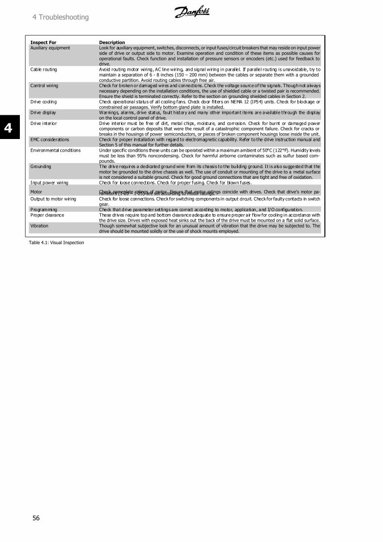
7/16/2019 1. D & E Frame.pdf
http://slidepdf.com/reader/full/1-d-e-framepdf 56/197
Inspect For Description Auxiliary equipment Look for auxiliary equipment, switches, disconnects, or input fuses/circuit breakers that may reside on input power
side of drive or output side to motor. Examine operation and condition of these items as possible causes foroperational faults. Check function and installation of pressure sensors or encoders (etc.) used for feedback todrive.
Cable routing Avoid routing motor wiring, AC line wiring, and signal wiring in parallel. If parallel routing is unavoidable, try tomaintain a separation of 6 - 8 inches (150 – 200 mm) between the cables or separate them with a groundedconductive partition. Avoid routing cables through free air.
Control wiring Check for broken or damaged wires and connections. Check the voltage source of the signals. Though not alwaysnecessary depending on the installation conditions, the use of shielded cable or a twisted pair is recommended.Ensure the shield is terminated correctly. Refer to the section on grounding shielded cables in Section 2.
Drive cool ing Check operational status of al l cool ing fans. Check door fi lters on NEMA 12 (IP54) units. Check for blockage orconstrained air passages. Verify bottom gland plate is installed.
Drive display Warnings, alarms, drive status, fault history and many other important items are available through the displayon the local control panel of drive.
Drive interior Drive interior must be free of dirt, metal chips, moisture, and corrosion. Check for burnt or damaged powercomponents or carbon deposits that were the result of a catastrophic component failure. Check for cracks orbreaks in the housings of power semiconductors, or pieces of broken component housings loose inside the unit.
EMC considerations Check for proper installation with regard to electromagnetic capability. Refer to the drive instruction manual andSection 5 of this manual for further details.
Environmental conditions Under specific conditions these units can be operated within a maximum ambient of 50°C (122°F). Humidity levelsmust be less than 95% noncondensing. Check for harmful airborne contaminates such as sulfur based com-pounds.
Grounding The drive requires a dedicated ground wire from its chassis to the building ground. It is also suggested that themotor be grounded to the drive chassis as well. The use of conduit or mounting of the drive to a metal surfaceis not considered a suitable ground. Check for good ground connections that are tight and free of oxidation.
Input power wiring Check for loose connections. Check for proper fusing. Check for blown fuses.
Motor Check nameplate ratings of motor. Ensure that motor ratings coincide with drives. Check that drive's motor pa-rameters (1-20 – 1-25) are set according to motor ratings.Output to motor wiring Check for loose connections. Check for switching components in output circuit. Check for faulty contacts in switch
gear.Programming Check that drive parameter settings are correct according to motor, application, and I/O configurat ion.Proper clearance These drives require top and bottom clearance adequate to ensure proper air flow for cooling in accordance with
the drive size. Drives with exposed heat sinks out the back of the drive must be mounted on a flat solid surface. Vibration Though somewhat subjective look for an unusual amount of vibration that the drive may be subjected to. The
drive should be mounted solidly or the use of shock mounts employed.
Table 4.1: Visual Inspection
4 Troubleshooting
56
4

7/16/2019 1. D & E Frame.pdf
http://slidepdf.com/reader/full/1-d-e-framepdf 57/197
4.5 Fault Symptoms
4.5.1 No display
The LCP display provides two display indications. One by means of the
backlit LCD alphanumeric display. The other is three LED indicators lights
near the bottom of the LCP. If the green power on LED is illuminated but
the backlit display is dark, this indicates that the LCP itself is defective
and must be replaced.
Be certain, however, that the display is completely dark. Having a single character in the upper corner of the LCP or just a dot indicates that communications
may have failed with the control card. This is typically seen when a serial bus communication option has been installed in the drive and is either not
connected properly or is malfunctioning.
If neither indication is available, then the source of the problem may be elsewhere. Proceed to the No Display test (6.3.1) to carry out further trouble-
shooting steps.
4.5.2 Intermittent display
Cutting out or flashing of the entire display and power LED indicates that the power supply (SMPS) is shutting down as a result of being overloaded. This
may be due to improper control wiring or a fault within the drive itself.
The first step is to rule out a problem in the control wiring. To do this, disconnect all control wiring by unplugging the control terminal blocks from the
control card.
If the display stays lit, then the problem is in the control wiring (external to the drive). All control wiring should be checked for shorts or incorrect
connections.
If the display continues to cut out, follow the procedure for No Display as though the display were not lit at all.
4.5.3 Motor will not run
In the event that this symptom is detected, first verify that the unit is properly power up (display is lit) and that there are no warning or alarm messages
displayed. The most common cause of this is ei ther incorrect control logic or an incorrectly programmed drive. Such occurrences will result in one or more
of the following status messages being displayed.
LCP Stop
The “OFF key has been pressed. Line 2 of the display will also be flashing when this occurs.
Press the AUTO ON or HAND ON key.
Standby
This indicates that there is no start signal at terminal 18.
Ensure that a start command is present at terminal 18. Refer to the Input Terminal Signal Test (6.3.16).
Unit ready
Terminal 27 is low (no signal).
Ensure that terminal 27 is logic “1”. Refer to the Input Terminal Signal Test (6.3.16).
4 Troubleshooting
57
4
7/16/2019 1. D & E Frame.pdf
http://slidepdf.com/reader/full/1-d-e-framepdf 58/197
Run OK, 0 Hz
This indicates that a run command has been given to the drive but the reference (speed command) is zero or missing.
Check control wiring to ensure that the proper reference signal is present at the drive input terminals and that the unit is properly programmed to accept
the signal provided. Refer to the Input Terminal Signal Test (6.3.16).
Off 1 (2 or 3)
This indicates that bit #1 (or #2, or #3) in the control word is logic “0”. This will only occur when the drive is being controlled via the serial communication
bus.
A correct control word must be transmitted to the drive over the communication bus to correct this.
STOP
One of the digital input terminals 18, 19, 27, 29, 32, or 33 (parameter 5-1) is programmed for “Stop Inverse” and the corresponding terminal is low (logic
“0”).
Ensure that the above parameters are programmed correctly and that any digital input programmed for “Stop Inverse” is high (logic “1”).
Display Indication That the Unit is Functioning, but No Output
Check that parameter 14-22 is not set to “Run With Inverter Disabled”.
If the unit is equipped with external 24 VDC option, check that the main power is applied to the drive.
Note: In this case, the display will alternately flash Warning 8.
4.5.4 Incorrect motor operation
Occasionally, a fault can occur where the motor will continue to run, but not in the correct manner. The symptoms and causes may vary considerably.
Many of the possible problems are listed below by symptom along with recommended procedures for determining their causes.
Wrong speed/unit will not respond to command
Possible incorrect reference (speed command).
Ensure that the unit is programmed correctly according to the reference signal being used, and that all reference limits are set correctly as well. Perform
Input Terminal Signal Test (6.3.16) to check for faulty reference signals.
Motor speed unstable
Possible incorrect parameter settings, faulty current feedback circuit, loss of motor (output) phase.
Check settings of all motor parameters, including all motor compensation settings (Slip Compensation, Load Compensation, etc.) For Closed Loop oper-
ation, check PID settings. Perform Input Terminal Signal Test (6.3.16) to check for faulty reference signals. Perform Output Phase Imbalance Test (6.3.10)
to check for loss of motor phase.
Motor runs rough
Possible over magnetization (incorrect motor settings), or an IGBT misfiring. Note: Motor may also stall when loaded or the drive may trip occasionally
on Alarm 13.
Check setting of all motor parameters. Perform Output Phase Imbalance Test (6.3.10).
If output voltage is unbalanced, perform Gate Drive Signal Test (6.3.11).
4 Troubleshooting
58
4
7/16/2019 1. D & E Frame.pdf
http://slidepdf.com/reader/full/1-d-e-framepdf 59/197
Motor draws high current but cannot start
Possible open winding in motor or open phase in connection to motor.
Perform Output Phase Imbalance Test (6.3.10) to ensure drive is providing correct output (see Motor Runs Rough above).
Run AMA to check motor for open windings and unbalanced resistance. Inspect all motor wiring connections.
Motor will not brake
Possible fault in brake circuit. Possible incorrect setting in brake parameters. Ramp down time too short. Note: May be accompanied by an alarm or
warning message.
Check all brake parameters and ramp down time (parameters 2-0 and 3-4).
Perform Brake Check (6.3.13).
4.6 Warning/Alarm Messages
4.6.1 Warning/alarm code list
A warning or an alarm is signalled by the LEDs on the front of the frequency converter and by a code on the display.
A warning indicates a condition that may require attention or a trend that may eventually require attention. A warning remains active until the cause is
no longer present. Under some circumstances motor operation may continue.
A trip is the action when an alarm has appeared. The trip removes power to the motor and can be reset after the condition has been cleared by pressing
the reset button or through a digital input (parameter 5-1). The event that caused an alarm cannot damage the drive or cause a dangerous condition.
Alarms must be reset to restart operation once their cause has been rectified.
This may be done in three ways:
1. Pressing the reset button on the control panel keypad.
2. A digital reset input.
3. Serial communication/optional fieldbus reset signal.
NB! After a manual reset using the [RESET] button on the , the [AUTO ON] button must be pressed to restart the motor.
A trip lock is an action when an alarm occurs which may cause damage to the frequency converter or connected equipment. Power is removed from
the motor. A trip lock can only be reset after the condition is cleared by cycling power. Once the problem has been rectified, only the alarm continues
flashing until the frequency converter is reset.
4 Troubleshooting
59
4

7/16/2019 1. D & E Frame.pdf
http://slidepdf.com/reader/full/1-d-e-framepdf 60/197
An X marked in the table below means that action occurs. A warning precedes an alarm.
No. Description Warning Alarm/Trip Alarm/Trip Lock
1 10 volts low X2 Live zero error (X) (X)3 No motor (X)4 Mains phase loss (X) (X) (X)5 DC link voltage high X6 DC link voltage low X7 DC overvoltage X X8 DC under voltage X X9 Inverter overloaded X X10 Motor over temperature (X) (X)11 Motor thermistor over temperature (X) (X)12 Torque limit X X13 Over current X X X14 Earth (ground) fault X X X15 Hardware mismatch X X16 Short circuit X X17 Control word timeout (X) (X)22 Hoist mechanical brake X23 Internal fan fault X24 External fan fault X25 Brake resistor short circuit X26 Brake resistor power limit (X) (X)27 Brake chopper fault X X
28 Brake check failed (X) (X)29 Heatsink temp X X X30 Motor phase U missing (X) (X) (X)31 Motor phase V missing (X) (X) (X)32 Motor phase W missing (X) (X) (X)33 Inrush fault X X34 Fieldbus communication fault X X36 Mains failure X X38 Internal fault X X39 Heatsink sensor X X40 Overload of Digital Output Terminal 27 (X)41 Overload of Digital Output Terminal 29 (X)42 Overload of Digital Output on X30/6 or Overload of Digital
Output on X30/7(X)
46 Power card supply X X47 24 V supply low X X X48 1.8 V supply low X X49 Speed limit X
50 AMA calibration failed X51 AMA check Unom and Inom X
52 AMA low Inom X
53 AMA motor too big X
Table 4.2: Warning/alarm code list
4 Troubleshooting
60
4

7/16/2019 1. D & E Frame.pdf
http://slidepdf.com/reader/full/1-d-e-framepdf 61/197
No. Description Warning Alarm/Trip Alarm/Trip Lock
54 AMA motor too small X55 AMA parameter out of range X56 AMA interrupted by user X57 AMA timeout X58 AMA internal fault X X59 Current limit X60 External interlock X61 Encoder loss (X) (X)62 Output frequency at maximum limit X X
63 Mechanical brake low (X)64 Voltage limit X
65 Control board over temperature X X X66 Heat sink temperature low X67 Option configuration has changed X68 Safe stop activated (X) (X)1)
69 Power card temperature X X70 Illegal FC configuration X71 PTC 1 safe stop X X72 Dangerous failure X X X73 Safe stop auto restart X79 Illegal PS config X X80 Drive initialized to default value X81 CSIV corrupt X82 CSIV parameter error X90 Encoder loss (X) (X)
91 Analogue input 54 wrong settings X92 No flow (X) (X)
93 Dry pump (X) (X)94 End of curve (X) (X)95 Broken belt (X) (X)96 Start delayed (X)97 Stop delayed (X)98 Clock fault X100-199 See Operating Instructions for MCO 305200 Fire mode (X)201 Fire mode was active (X)202 Fire mode limits exceeded (X)243 Brake IGBT X X244 Heatsink temperature X X X245 Heatsink sensor X X246 Power card supply X X247 Power card temperature X X248 Illegal PS config X X
250 New spare part X251 New type code X X
Table 4.3: Alarm/Warning code list
(X) Programmable: dependent on parameter setting.
1) Cannot be Auto reset via parameter selection.
LED indication
Warning yellow
Alarm flashing red
Trip locked yellow and red
4 Troubleshooting
61
4

7/16/2019 1. D & E Frame.pdf
http://slidepdf.com/reader/full/1-d-e-framepdf 62/197
WARNING 1, 10 volts low
The control card voltage is below 10 V from terminal 50.
Remove some of the load from terminal 50, as the 10 V supply is over-
loaded. Max. 15 mA or minimum 590 Ω.
This condition can be caused by a short in a connected potentiometer or
improper wiring of the potentiometer.
Troubleshooting: Remove the wiring from terminal 50. If the warning
clears, the problem is with the customer wiring. If the warning does not
clear, replace the control card.
WARNING/ALARM 2, Live zero error
This warning or alarm will only appear if programmed by the user in pa-
rameter 6-01, Live Zero Timeout Function. The signal on one of the
analog inputs is less than 50% of the minimum value programmed for
that input. This condition can be caused by broken wiring or faulty device
sending the signal.
Troubleshooting:
Check connections on all the analog input terminals. Control
card terminals 53 and 54 for signals, terminal 55 common. MCB
101 terminals 11 and 12 for signals, terminal 10 common. MCB
109 terminals 1, 3, 5 for signals, terminals 2, 4, 6 common).
Check that the drive programming and switch settings match
the analog signal type.
Perform the Input Terminal Signal Test in Section 6.3.16.
WARNING/ALARM 3, No motor
No motor has been connected to the output of the frequency converter.
This warning or alarm will only appear if programmed by the user in pa-
rameter 1-80, Function at Stop.
Troubleshooting: Check the connection between the drive and the mo-
tor.
WARNING/ALARM 4, Mains phase loss A phase is missing on the supply side, or the mains voltage imbalance is
too high. This message also appears for a fault in the input rectifier on
the frequency converter. Options are programmed at parameter
14-12, Function at Mains Imbalance
Troubleshooting: Check the supply voltage and supply currents to the
frequency converter. See Section 5.1.2 for troubleshooting details.
WARNING 5, DC link voltage high
The intermediate circuit voltage (DC) is higher than the high voltage
warning limit. The limit is dependent on the drive voltage rating. The
frequency converter is still active.
See ratings table in Section 1.9 for the voltage limits.
WARNING 6, DC link voltage low
The intermediate circuit voltage (DC) is lower than the low voltage warn-
ing limit. The limit is dependent on the drive voltage rating. The frequency
converter is still active.
See ratings table in Section 1.9 for the voltage limits.
WARNING/ALARM 7, DC overvoltage
If the intermediate circuit voltage exceeds the limit, the frequency con-
verter trips after a time.
Troubleshooting:
Connect a brake resistor
Extend the ramp time
Change the ramp type
Activate functions in par. 2-10 Brake Function
Increase par. 14-26 Trip Delay at Inverter Fault
See ratings table in Section 1.9 for the voltage limits. See Section 5.1.1
for troubleshooting details.
WARNING/ALARM 8, DC under voltage
If the intermediate circuit voltage (DC) drops below the under voltage
limit, the frequency converter checks if a 24 V backup supply is connec-
ted. If no 24 V backup supply is connected, the frequency converter trips
after a fixed time delay. The time delay varies with unit size.
See ratings table in Section 1.9 for the voltage limits.
Troubleshooting:
Check that the supply voltage matches the frequency converter
voltage.
Perform Input voltage test (Section 6.3.2)
Perform soft charge and rectifier circuit test (Section 6.2.1 or
6.2.3)
WARNING/ALARM 9, Inverter overloaded
The frequency converter is about to cut out because of an overload (too
high current for too long). The counter for electronic, thermal inverter
protection gives a warning at 98% and trips at 100%, while giving an
alarm. The frequency converter cannot be reset until the counter is below
90%.
The fault is that the frequency converter is overloaded by more than
100% for too long.
Troubleshooting:
Compare the output current shown on the LCP keypad with the
drive rated current.
Compare the output current shown on the LCP keypad with
measured motor current.
Display the Thermal Drive Load on the keypad and monitor the
value. When running above the drive continuous current rating,
the counter should increase. When running below the drive con-
tinuous current rating, the counter should decrease.
Note: See the derating section in the Design Guide for more details if a
high switching frequency is required.
WARNING/ALARM 10, Motor overload temperature
According to the electronic thermal protection (ETR), the motor is too hot.
Select whether the frequency converter gives a warning or an alarm when
the counter reaches 100% in par. 1-90 Motor Thermal Protection . The
fault is that the motor is overloaded by more than 100% for too long.
Troubleshooting:
Check if motor is over heating.
If the motor is mechanically overloaded
That the motor par. 1-24 Motor Current is set correctly.
Motor data in parameters 1-20 through 1-25 are set correctly.
The setting in parameter 1-91, Motor External Fan.
Run AMA in parameter 1-29.
WARNING/ALARM 11, Motor thermistor over temp
The thermistor or the thermistor connection is disconnected. Select
whether the frequency converter gives a warning or an alarm when the
counter reaches 100% in par. 1-90 Motor Thermal Protection .
4 Troubleshooting
62
4
7/16/2019 1. D & E Frame.pdf
http://slidepdf.com/reader/full/1-d-e-framepdf 63/197
Troubleshooting:
Check if motor is over heating.
Check if the motor is mechanically overloaded.
Check that the thermistor is connected correctly between ter-
minal 53 or 54 (analog voltage input) and terminal 50 (+10 V
supply), or between terminal 18 or 19 (digital input PNP only)
and terminal 50.
If a KTY sensor is used, check for correct connection between
terminal 54 and 55.
If using a thermal switch or thermistor, check the programming
of parameter 1-93 matches sensor wiring.
If using a KTY sensor, check the programming of parameters
1-95, 1-96, and 1-97 match sensor wiring.
WARNING/ALARM 12, Torque limit
The torque is higher than the value in par. 4-16 Torque Limit Motor
Mode (in motor operation) or the torque is higher than the value in par.
4-17 Torque Limit Generator Mode (in regenerative operation). Parame-
ter 14-25 can be used to change this from a warning only condition to a
warning followed by an alarm.
See section 5.1 for troubleshooting.
WARNING/ALARM 13, Over Current
The inverter peak current limit (approx. 200% of the rated current) is
exceeded. The warning lasts about 1.5 sec., then the frequency converter
trips and issues an alarm. If extended mechanical brake control is selec-
ted, trip can be reset externally.
Troubleshooting:
This fault may be caused by shock loading or fast acceleration
with high inertia loads.
Turn off the frequency converter. Check if the motor shaft can
be turned.
Check that the motor size matches the frequency converter.
Incorrect motor data in parameters 1-20 through 1-25.
See section 1.9 for current trip points.
ALARM 14, Earth (ground) fault
There is a discharge from the output phases to earth, either in the cable
between the frequency converter and the motor or in the motor itself.
See section 1.9 for trip levels.
Troubleshooting:
Turn off the frequency converter and remove the earth fault.
Measure the resistance to ground of the motor leads and the
motor with a megohmmeter to check for earth faults in the mo-
tor.
Perform the current sensor test (section 6.3.14).
See section 5.2 for more details.
ALARM 15, Hardware mismatch
A fitted option is not operational with the present control board hardware
or software.
Record the value of the following parameters and contact your Danfoss
supplier:
15-40 FC Type
15-41 Power Section
15-42 Voltage
15-43 Software Version
15-45 Actual Typecode String
15-49 SW ID Control Card
15-50 SW ID Power Card
15-60 Option Mounted (for each option slot)
15-61 Option SW Version (for each option slot)
ALARM 16, Short circuit
There is short-circuiting in the motor or on the motor terminals.
Turn off the frequency converter and remove the short-circuit.
See section 1.9 for trip levels.
WARNING/ALARM 17, Control word timeout
There is no communication to the frequency converter.
The warning will only be active when par. 8-04 Control Word Timeout
Function is NOT set to OFF.
If par. 8-04 Control Word Timeout Function is set to Stop and Trip , a
warning appears and the frequency converter ramps down until it trips,
while giving an alarm.
Troubleshooting:
Check connections on the serial communication cable.
Increasepar. 8-03 Control Word Timeout Time
Check operation of the communication equipment.
Verify proper installation based on EMC requirements. See sec-
tion 5.
WARNING 22, Hoist mechanical brake
Report value will show what kind it is.
0 = The torque reference was not reached before timeout.
1 = There was no brake feedback before timeout.
WARNING 23, Internal fan fault
The fan warning function is an extra protection function that checks if the
fan is running / mounted. The fan warning can be disabled in par.
14-53 Fan Monitor ([0] Disabled).
For the D, E, and F Frame drives, the regulated voltage to the fans is
monitored.
Troubleshooting:
Check fan resistance (see section 6.2.9 or 6.2.10).
Check soft charge fuses (see section 6.2.1 or 6.2.3).
WARNING 24, External fan fault
The fan warning function is an extra protection function that checks if the
fan is running / mounted. The fan warning can be disabled in par.
14-53 Fan Monitor ([0] Disabled).
For the D, E, and F Frame drives, the regulated voltage to the fans is
monitored.
Troubleshooting:
Check fan resistance (see section 6.2.9 or 6.2.10).
Check soft charge fuses (see section 6.2.1 or 6.2.3).
WARNING 25, Brake resistor short circuit
The brake resistor is monitored during operation. If it short circuits, the
brake function is disconnected and the warning appears. The frequency
converter still works, but without the brake function. Turn off the fre-
quency converter and replace the brake resistor (see par. 2-15 Brake
Check ).
4 Troubleshooting
63
4
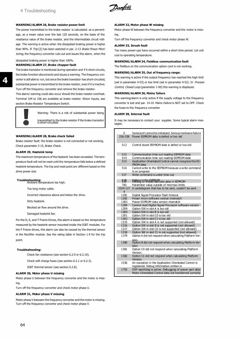
7/16/2019 1. D & E Frame.pdf
http://slidepdf.com/reader/full/1-d-e-framepdf 64/197
WARNING/ALARM 26, Brake resistor power limit
The power transmitted to the brake resistor is calculated: as a percent-
age, as a mean value over the last 120 seconds, on the basis of the
resistance value of the brake resistor, and the intermediate circuit volt-
age. The warning is active when the dissipated braking power is higher
than 90%. If Trip [2] has been selected in par. 2-13 Brake Power Moni-
toring , the frequency converter cuts out and issues this alarm, when the
dissipated braking power is higher than 100%.
WARNING/ALARM 27, Brake chopper fault
The brake transistor is monitored during operation and if it short-circuits,
the brake function disconnects and issues a warning. The frequency con-
verter is still able to run, but since the brake transistor has short-circuited,
substantial power is transmitted to the brake resistor, even if it is inactive.
Turn off the frequency converter and remove the brake resistor.
This alarm/ warning could also occur should the brake resistor overheat.
Terminal 104 to 106 are available as brake resistor. Klixon inputs, see
section Brake Resistor Temperature Switch.
Warning: There is a risk of substantial power being
transmitted to the brake resistor if the brake transistoris short-circuited.
WARNING/ALARM 28, Brake check failed
Brake resistor fault: the brake resistor is not connected or not working.
Check parameter 2-15, Brake Check.
ALARM 29, Heatsink temp
The maximum temperature of the heatsink has been exceeded. The tem-
perature fault will not be reset until the temperature falls below a defined
heatsink temperature. The trip and reset point are different based on the
drive power size.
Troubleshooting: Ambient temperature too high.
Too long motor cable.
Incorrect clearance above and below the drive.
Dirty heatsink.
Blocked air flow around the drive.
Damaged heatsink fan.
For the D, E, and F Frame Drives, this alarm is based on the temperature
measured by the heatsink sensor mounted inside the IGBT modules. For
the F Frame drives, this alarm can also be caused by the thermal sensor
in the Rectifier module. See the rating table in Section 1.9 for the trip
point.
Troubleshooting:
Check fan resistance (see section 6.2.9 or 6.2.10).
Check soft charge fuses (see section 6.2.1 or 6.2.3).
IGBT thermal sensor (see section 6.2.8).
ALARM 30, Motor phase U missing
Motor phase U between the frequency converter and the motor is miss-
ing.
Turn off the frequency converter and check motor phase U.
ALARM 31, Motor phase V missing
Motor phase V between the frequency converter and the motor is missing.
Turn off the frequency converter and check motor phase V.
ALARM 32, Motor phase W missing
Motor phase W between the frequency converter and the motor is miss-
ing.
Turn off the frequency converter and check motor phase W.
ALARM 33, Inrush fault
Too many power-ups have occurred within a short time period. Let unit
cool to operating temperature.
WARNING/ALARM 34, Fieldbus communication fault
The fieldbus on the communication option card is not working.
WARNING/ALARM 35, Out of frequency range:
This warning is active if the output frequency has reached the high limit
(set in parameter 4-53) or low limit (set in parameter 4-52). In Process
Control, Closed Loop (parameter 1-00) this warning is displayed.
WARNING/ALARM 36, Mains failure
This warning/alarm is only active if the supply voltage to the frequency
converter is lost and par. 14-10 Mains Failure is NOT set to OFF. Check
the fuses to the frequency converter
ALARM 38, Internal fault
It may be necessary to contact your supplier. Some typical alarm mes-sages:
0 Serial port cannot be initialized. Serious hardware failure256-258 Power EEPROM data is defect or too old
512 Control board EEPROM data is defect or too old
513 Communication time out reading EEPROM data514 Communication time out reading EEPROM data515 Application Orientated Control cannot recognize the EE-
PROM data516 Cannot write to the EEPROM because a write command
is on progress517 Write command is under time out
518 Failure in the EEPROM519 Missing or invalid Barcode data in EEPROM783 Parameter value outside of min/max limits
1024-1279
A cantelegram that has to be sent, couldn't be sent
1281 Digital Signal Processor flash timeout1282 Power micro software version mismatch1283 Power EEPROM data version mismatch1284 Cannot read Digital Signal Processor software version1299 Option SW in slot A is too old1300 Option SW in slot B is too old1301 Option SW in slot C0 is too old1302 Option SW in slot C1 is too old1315 Option SW in slot A is not supported (not allowed)1316 Option SW in slot B is not supported (not allowed)1317 Option SW in slot C0 is not supported (not allowed)1318 Option SW in slot C1 is not supported (not allowed)1379 Option A did not respond when calculating Platform Ver-
sion.1380 Option B did not respond when calculating Platform Ver-
sion.1381 Option C0 did not respond when calculating Platform
Version.1382 Option C1 did not respond when calculating Platform
Version.1536 An exception in the Application Orientated Control is
registered. Debug information written in1792 DSP watchdog is active. Debugging of power part data
Motor Orientated Control data not transferred correctly
4 Troubleshooting
64
4

7/16/2019 1. D & E Frame.pdf
http://slidepdf.com/reader/full/1-d-e-framepdf 65/197
2049 Power data restarted2064-2072 H081x: option in slot x has restarted2080-2088 H082x: option in slot x has issued a powerup-wait2096-2104 H083x: option in slot x has issued a legal powerup-wait
2304 Could not read any data from power EEPROM2305 Missing SW version from power unit2314 Missing power unit data from power unit2315 Missing SW version from power unit2316 Missing io_statepage from power unit2324 Power card configuration is determined to be incorrect
at power up2325 A power card has stopped communicating while main
power is applied2326 Power card configuration is determined to be incorrect
after the delay for power cards to register2327 Too many power card locations have been registered
as present2330 Power size information between the power cards does
not match2561 No communication from DSP to ATACD2562 No communication from ATACD to DSP (state running)2816 Stack overflow Control board module2817 Scheduler slow tasks2818 Fast tasks2819 Parameter thread2820 Stack overflow2821 Serial port overf low
2822 USB port overflow2836 cfListMempool to small3072-5122 Parameter value is outside its limits
5123 Option in slot A: Hardware incompatible with Controlboard hardware
5124 Option in slot B: Hardware incompatible with Controlboard hardware
5125 Option in slot C0: Hardware incompatible with Controlboard hardware
5126 Option in slot C1: Hardware incompatible with Controlboard hardware
5376-6231 Out of memory
ALARM 39, Heatsink sensor
No feedback from the heatsink temperature sensor.
The signal from the IGBT thermal sensor is not available on the power
card. The problem could be on the power card, on the gate drive card,
or the ribbon cable between the power card and gate drive card.
WARNING 40, Overload of Digital Output Terminal 27
Check the load connected to terminal 27 or remove short-circuit connec-
tion. Check par. 5-00 Digital I/O Mode and par. 5-01 Terminal 27 Mode .
WARNING 41, Overload of Digital Output Terminal 29
Check the load connected to terminal 29 or remove short-circuit connec-
tion. Check par. 5-00 Digital I/O Mode and par. 5-02 Terminal 29 Mode .
WARNING 42, Overload of Digital Output on X30/6 or Overload
of Digital Output on X30/7
For X30/6, check the load connected to X30/6 or remove short-circuit
connection. Check par. 5-32 Term X30/6 Digi Out (MCB 101) .
For X30/7, check the load connected to X30/7 or remove short-circuit
connection. Check par. 5-33 Term X30/7 Digi Out (MCB 101) .
ALARM 46, Power card supply
The supply on the power card is out of range.
There are three power supplies generated by the switch mode power
supply (SMPS) on the power card: 24 V, 5V, +/- 18V. When powered with
24 VDC with the MCB 107 option, only the 24 V and 5 V supplies are
monitored. When powered with three phase mains voltage, all three sup-
plied are monitored.
WARNING 47, 24 V supply low
The 24 VDC is measured on the control card. The external 24 VDC backup
power supply may be overloaded, otherwise contact your supplier.
WARNING 48, 1.8 V supply low
The 1.8 Volt DC supply used on the control card is outside of allowable
limits. The power supply is measured on the control card.
WARNING 49, Speed limit
The speed is not within the specified range in par. 4-11 Motor Speed Low
Limit [RPM] and par. 4-13 Motor Speed High Limit [RPM] .
ALARM 50, AMA calibration failed
Contact your supplier.
ALARM 51, AMA check Unom and Inom
The setting of motor voltage, motor current, and motor power is pre-
sumably wrong. Check the settings.
ALARM 52, AMA low Inom
The motor current is too low. Check the settings.
ALARM 53, AMA motor too big
The motor is too big for the AMA to be carried out.
ALARM 54, AMA motor too small
The motor is too big for the AMA to be carried out.
ALARM 55, AMA parameter out of range
The parameter values found from the motor are outside acceptable
range.
ALARM 56, AMA interrupted by user
The AMA has been interrupted by the user.
ALARM 57, AMA timeout
Try to start the AMA again a number of times, until the AMA is carried
out. Please note that repeated runs may heat the motor to a level where
the resistance Rs and Rr are increased. In most cases, however, this is
not critical.
ALARM 58, AMA internal fault
Contact your supplier.
WARNING 59, Current limit
The current is higher than the value in par. 4-18, Current Limit .
WARNING 60, External interlock
External interlock has been activated. To resume normal operation, apply
24 VDC to the terminal programmed for external interlock and reset the
frequency converter (via serial communication, digital I/O, or by pressing
reset button on keypad).
WARNING 61, Tracking error
An error has been detected between calculated motor speed and speed
measurement from feedback device. The function for Warning/Alarm/
Disable is set in par 4-30, Motor Feedback Loss Function , error setting in
par 4-31, Motor Feedback Speed Error , and the allowed error time in par
4-32, Motor Feedback Loss Timeout . During a commissioning procedure
the function may be effective.
WARNING 62, Output frequency at maximum limit
The output frequency is higher than the value set in par. 4-19 Max Output
Frequency
ALARM 63, mechanical brake Low
The actual motor current has not exceeded the release-brake current
within the start-delay time window.
WARNING 64, Voltage limit
The load and speed combination demands a motor voltage higher than
the actual DC link voltage.
4 Troubleshooting
65
4
7/16/2019 1. D & E Frame.pdf
http://slidepdf.com/reader/full/1-d-e-framepdf 66/197
WARNING/ALARM/TRIP 65, Control card over temperature
Control card over temperature: The cutout temperature of the control
card is 80° C.
WARNING 66, Heatsink temperature low
This warning is based on the temperature sensor in the IGBT module.
See the ratings table in Section 1.9 for the temperature reading that will
trigger this warning.
Troubleshooting:
The heatsink temperature measured as 0° C could indicate that the tem-
perature sensor is defective causing the fan speed to increase to the
maximum. If the sensor wire between the IGBT and the gate drive card
is disconnected, this warning would result. Also, check the IGBT thermal
sensor (see section 6.2.8).
ALARM 67, Option module configuration has changed
One or more options have either been added or removed since the last
power-down.
ALARM 68, Safe stop activated
Safe stop has been activated. To resume normal operation, apply 24 VDC
to terminal 37, then send a reset signal (via Bus, Digital I/O, or by press-ing the reset key. See parameter 5-19, Terminal 37 Safe Stop.
ALARM 69, Power card temperature
The temperature sensor on the power card is either too hot or too cold.
See the ratings table in Section 1.9 for the high and low temperatures
that can cause this alarm.
Troubleshooting:
Check the operation of the door fans.
Check that the filters for the door fans are not blocked.
Check that the gland plate is properly installed on IP 21 and IP
54 (NEMA 1 and NEMA 12) drives.
ALARM 70, Illegal FC Configuration
Actual combination of control board and power board is illegal.
WARNING/ALARM 71, PTC 1 safe stop
Safe Stop has been activated from the MCB 112 PTC Thermistor Card
(motor too warm). Normal operation can be resumed when the MCB 112
applies 24 V DC to T-37 again (when the motor temperature reaches an
acceptable level) and when the Digital Input from the MCB 112 is deac-
tivated. When that happens, a reset signal must be is be sent (via serial
communication, digital I/O, or by pressing reset button on keypad). Note
that if automatic restart is enabled, the motor may start when the fault
is cleared.
ALARM 72, Dangerous failure
Safe stop with trip lock. Unexpected signal levels on safe stop and digital
input from the MCB 112 PTC thermistor card.
Warning 73, Safe stop auto restart
Safe stopped. Note that with automatic restart enabled, the motor may
start when the fault is cleared.
ALARM 79, Illegal power section configuration
The scaling card is the incorrect part number or not installed. Also MK102
connector on the power card is not installed.
ALARM 80, Drive initialized to default value
Parameter settings are initialized to default settings after a manual reset.
WARNING 81, CSIV corrupt
CSIV file has syntax errors.
WARNING 82, CSIV parameter error
CSIV has failed to record a parameter.
ALARM 91, Analog input 54 wrong settings
Switch S202 has to be set in position OFF (voltage input) when a KTY
sensor is connected to analog input terminal 54.
ALARM 92, No flow
A no-load situation has been detected in the system. See parameter
group 22-2.
ALARM 93, Dry pump
A no-flow situation and high speed indicates that the pump has run dry.
See parameter group 22-2.
ALARM 94, End of curve
Feedback stays lower than the set point which may indicate leakage in
the pipe system. See parameter group 22-5.
ALARM 95, Broken belt
Torque is below the torque level set for no load, indicating a broken belt.
See parameter group 22-6.
ALARM 96, Start delayed
Motor start has been delayed due to short-cycle protection active. See
parameter group 22-7.
WARNING 97, Stop delayed
Stopping the motor has been delayed due to short cycle protection is
active. See parameter group 22-7.
WARNING 98, Clock fault
Clock Fault. Time is not set or RTC clock (if mounted) has failed. See
parameter group 0-7.
WARNING 200, Fire mode
The input command fire mode is active. See parameter group 24-0.
WARNING 201, Fire mode was active
Fire mode has been active. See parameter group 0-7.
WARNING 202, Fire mode limits exceeded
One or more warranty voiding alarms have been suppressed during fire
mode operation. See parameter group 0-7.
ALARM 243, Brake IGBT
This alarm is only for F Frame drives. It is equivalent to Alarm 27. The
report value in the alarm log indicates which power module generated
the alarm:
1 = left most inverter module.
2 = middle inverter module in F2 or F4 drive.
2 = right inverter module in F1 or F3 drive.
3 = right inverter module in F2 or F4 drive.
5 = rectifier module.
ALARM 244, Heatsink temperature
This alarm is only for F Frame drives. It is equivalent to Alarm 29. The
report value in the alarm log indicates which power module generated
the alarm:
1 = left most inverter module.
2 = middle inverter module in F2 or F4 drive.
2 = right inverter module in F1 or F3 drive.
3 = right inverter module in F2 or F4 drive.
5 = rectifier module.
4 Troubleshooting
66
4
7/16/2019 1. D & E Frame.pdf
http://slidepdf.com/reader/full/1-d-e-framepdf 67/197
ALARM 245, Heatsink sensor
This alarm is only for F Frame drives. It is equivalent to Alarm 39. The
report value in the alarm log indicates which power module generated
the alarm:
1 = left most inverter module.
2 = middle inverter module in F2 or F4 drive.
2 = right inverter module in F1 or F3 drive.
3 = right inverter module in F2 or F4 drive.
5 = rectifier module.
ALARM 246, Power card supply
This alarm is only for F Frame drives. It is equivalent to Alarm 46. The
report value in the alarm log indicates which power module generated
the alarm:
1 = left most inverter module.
2 = middle inverter module in F2 or F4 drive.
2 = right inverter module in F1 or F3 drive.
3 = right inverter module in F2 or F4 drive.
5 = rectifier module.
ALARM 247, Power card temperature
This alarm is only for F Frame drives. It is equivalent to Alarm 69. The
report value in the alarm log indicates which power module generated
the alarm:
1 = left most inverter module.
2 = middle inverter module in F2 or F4 drive.
2 = right inverter module in F1 or F3 drive.
3 = right inverter module in F2 or F4 drive.
5 = rectifier module.
ALARM 248, Illegal power section configuration
This alarm is only for F-frame drives. It is equivalent to Alarm 79. The
report value in the alarm log indicates which power module generated
the alarm:
1 = left most inverter module.
2 = middle inverter module in F2 or F4 drive.
2 = right inverter module in F1 or F3 drive.
3 = right inverter module in F2 or F4 drive.
5 = rectifier module.
ALARM 250, New spare part
The power or switch mode power supply has been exchanged. The fre-
quency converter type code must be restored in the EEPROM. Select thecorrect type code in par. 14-23 Typecode Setting according to the label
on the unit. Remember to select ‘Save to EEPROM’ to complete.
ALARM 251, New type code
The frequency converter has a new type code.
4.7 After Repair Tests
Following any repair to a drive or testing of a drive suspected of being faulty, the following procedure must be followed to ensure that all circuitry in the
drive is functioning properly before putting the unit into operation.
1. Perform visual inspection procedures as described in Table 3-1.
2. Perform static test procedures 6.2.1., 6.2.2 and 6.2.5 for D-frame size units or 6.2.3, 6.2.4 and 6.2.5 for E-frame size units to ensure drive is
safe to start.
3. Disconnect motor leads from output terminals (U, V, W) of drive.
4. Apply AC power to drive.
5. Give drive a run command and slowly increase reference (speed command) to approximately 40 Hz.
6. Using an analog volt meter or a DVM capable of measuring true RMS, measure phase-to-phase output voltage on all three phases: U to V, U to
W, V to W. Al l voltages must be balanced within 8 volts. If unbalanced voltage is measured, refer to Input Voltage Test (6.3.2).
7. Stop drive and remove input power. Allow 40 minutes for DC capacitors to fully discharge for E-frame size drives or 20 minutes for D-frame size
drives.
8. Reconnect motor leads to drive output terminals (U, V, W).
9. Reapply power and restart drive. Adjust motor speed to a nominal level.
10. Using a clamp-on style ammeter, measure output current on each output phase. All currents should be balanced. If unbalanced current is
measured, refer to Current Sensor Test (6.3.14).
4 Troubleshooting
67
4

7/16/2019 1. D & E Frame.pdf
http://slidepdf.com/reader/full/1-d-e-framepdf 68/197
5 Drive and Motor Applications
68
5

7/16/2019 1. D & E Frame.pdf
http://slidepdf.com/reader/full/1-d-e-framepdf 69/197
5 Drive and Motor Applications
5.1 Torque Limit, Current Limit, and Unstable Motor Operation
Excessive loading of the drive may result in warning or tripping on torque limit, over current, or inverter time. This is not a concern if the drive is properly
sized for the application and intermittent load conditions cause anticipated operation in torque limit or an occasional trip. However, nuisance or unexplained
occurrences may be the result of improperly setting specific parameters. The following parameters are important in matching the drive to the motor for
optimum operation. These setting need careful attention.
Parameter 1-03 sets the mode in which the drive will operate.
Parameters 1-20 through 1-29 match the drive to the motor and adapt to the motor characteristics.
Parameters 4-17 and 14-25 set the torque control features of the drive for the application.
Parameter 1-00, Configuration, sets the drive for open or closed loop operation or torque mode operation. In a closed loop configuration, a feedback
signal controls the drive speed. The settings for the PID controller play a key role for stable operation in closed loop, as described in the operator's manual.
In open loop, the drive calculates the torque requirement based on current measurements of the motor.
Parameter 1-03, Torque Characteristics, sets the drive for constant or variable torque operation. It is imperative that the correct torque characteristic is
selected, based on the application. If, for example, the load type is constant torque, such as a conveyor, and variable torque is selected, the drive may
have great difficulty starting the load, if started at all. Consult the factory if uncertain about the torque characteristics of an application.
Parameters 1-20 through 1-25 configure the drive for the connected motor. These are motor power, voltage, frequency, current, and rated motor speed.
Accurate setting of these parameters is very important. Enter the motor data required as listed on the motor nameplate. For effective and efficient load
control, the drive relies on this information for calculating the output waveform in response to the changing demands of the application.
Parameter 1-29 activates the automatic motor adaptation (AMA) function. When AMA is performed, the drive measures the electrical characteristics of
the motor and sets various drive parameters based on the findings. Two key parameter values set by this function are stator resistance and main reactance,
parameters 1-30 and 1-35. If unstable motor operation is experienced and AMA has not been performed, it should be done. AMA can only be performed
on single motor applications within the programming range of the drive. Consult the instruction manual for more on this function.
Parameters 1-30 and 1-35, as stated, should be set by the AMA function, values supplied by the motor manufacturer, or left at the factory default values.
Never adjust these parameters to random values even though it may seem to improve operation. Such adjustments can result in unpredictable operation
under changing conditions.
Parameter 4-17, Torque Limit, sets the limit for drive torque. The factory setting is 160% for FC 302 series and 110% for FC 102/202 series and will vary
with motor power setting. For example, a drive programmed to operate a smaller rated motor will yield a higher torque limit value than the same drive
programmed to operate a larger size motor. It is important that this value not be set too low for the requirements of the application. In some cases, i t
may be desirable to have a torque limit set at a lesser value. This offers protection for the application in that the drive will limit the torque. It may,
however, require higher torque at initial start up. Under these circumstances, nuisance tripping may occur.
Parameter 14-25, Trip Delay at Torque Limit, works in conjunction with torque limit. This parameter selects the length of time the drive operates in torque
limit prior to a trip. The factory default value is off. This means that the drive will not trip on torque limit, but it does not mean it will never trip from an
overload condition. Built into the drive is an internal inverter thermal protection circuit. This circuit monitors the output load on the inverter. If the load
exceeds 100% of the continuous rating of the drive, a timer is activated. If the load remains excessive long enough, the drive will trip on inverter time.
Adjustments cannot be made to alter this circuit. Improper parameter settings effecting load current can result in premature trips of this type. The timer
can be displayed.
5.1.1 Overvoltage trips
This trip occurs when the DC bus voltage reaches its DC bus alarm voltage high (see ratings tables in introductory section). Prior to the trip, the drive
will display a high voltage warning. Most times an over voltage condition is due to fast deceleration ramps with respect to the inertia of the load. During
deceleration of the load, inertia of the system acts to sustain the running speed. Once the motor frequency drops below the running speed, the load
begins overhauling the motor. At this point the motor becomes a generator and starts returning energy to the drive. This is called regenerative energy.
5 Drive and Motor Applications
69
5
7/16/2019 1. D & E Frame.pdf
http://slidepdf.com/reader/full/1-d-e-framepdf 70/197
Regeneration occurs when the speed of the load is greater than the commanded speed. This return voltage is rectified by the diodes in the IGBT modules
and raises the DC bus. If the amount of returned voltage is too high, the drive will trip.
There are a few ways to overcome this situation. One method is to reduce the deceleration rate so it takes longer for the drive to decelerate. A general
rule of thumb is that the drive can only decelerate the load slightly faster than it would take for the load to naturally coast to a stop. A second method
is to allow the overvoltage control circuit to take care of the deceleration ramp. When enabled the overvoltage control circuit regulates deceleration at a
rate that maintains the DC bus voltage at an acceptable level. One caution with overvoltage control is that it will not make corrections to unrealistic ramp
rates. For example, if the deceleration ramp needs to be 100 seconds due to the inertia, and the ramp rate is set at 3 seconds, overvoltage control will
initially engage and then disengage and allow the drive to trip. This is purposely done so the units operation is not misinterpreted. A third method in
controlling regenerated energy is with a dynamic brake. The drive monitors the level of the DC bus. Should the level become too high, the drive switches
the resistor across the DC bus and dissipates the unwanted energy into the external resistor bank mounted outside of the drive. This will actually increase
the rate of deceleration.
Less often is the case that the overvoltage condition is caused by the load while it is running at speed. In this case the dynamic brake option can be used
or the overvoltage control circuit. It works with the load in this way. As stated earlier, regeneration occurs when the speed of the load is greater than
the commanded speed. Should the load become regenerative while the drive is running at a steady state speed, the overvoltage circuit will increase the
frequency to match the speed of the load. The same restriction on the amount of influence applies. The drive will add about 10% to the base speed
before a trip occurs. Otherwise, the speed could continue to rise to potentially unsafe levels.
5.1.2 Mains phase loss trips
The drive actually monitors phase loss by monitoring the amount of ripple voltage on the DC bus. Ripple voltage on the DC bus is a product of a phase
loss. The main concern is that ripple voltage causes overheating in the DC bus capacitors and the DC coil. Left unchecked, the lifetime of the capacitors
and DC coil would be drastically reduced.
When the input voltage becomes unbalanced or a phase disappears completely, the ripple voltage increases causing the drive to trip and issue an Alarm
4. In addition to missing phase voltage, increased bus ripple can be caused by a line disturbance or imbalance. Line disturbances may be caused by line
notching, defective transformers or other loads that may be effecting the form factor of the AC waveform. Line imbalances which exceed 3% cause
sufficient DC bus ripple to initiate a trip.
Output disturbances can have the same effect of increased ripple voltage on the DC bus. A missing or lower than normal output voltage on one phasecan cause increased ripple on the DC bus. Should a mains imbalance trip occur, it is necessary to check both the input and output voltage of the drive.
Severe phase imbalance or phase loss can easily be detected with a volt meter. Line disturbances most likely need to be viewed on an oscilloscope.
Conduct tests for input phase imbalance, input waveform, and output phase imbalance as described in the chapter Troubleshooting .
5.1.3 Control logic problems
Problems with control logic can often be difficult to diagnose, since there is usually no associated fault indication. The typical complaint is simply that the
drive does not respond to a given command. There are two basic commands that must be given to any drive in order to obtain an output. First, the drive
must be told to run (start command). Second, the drive must be told how fast to run (reference or speed command).
The drives are designed to accept a variety of signals. First determine what types of signals the drive is receiving. There are six digital inputs (terminals
18, 19, 27, 29, 32, 33), two analog inputs (53 and 54), and the serial communication bus (68, 69). The presence of a correct reading will indicate that
the desired signal has been detected by the microprocessor of the drive. See the chapter Drive Inputs and Outputs .
Using the status information displayed by the drive is the best method of locating problems of this nature. By selecting within parameter group 0-2 LCP
Display, line 2 or 3 of the display can be set to indicate the signals coming in. The presence of a correct reading indicates that the desired signal is
detected by the microprocessor of the drive. This data also may be read in parameter group 16-6.
If there is not a correct indication, the next step is to determine whether the signal is present at the input terminals of the drive. This can be performed
with a voltmeter or oscilloscope in accordance with the 6.3.16, Input Terminal Signal Test.
If the signal is present at the terminal, the control card is defective and must be replaced. If the signal is not present, the problem is external to the drive.The circuitry providing the signal along with its associated wiring must then be checked.
5 Drive and Motor Applications
70
5

7/16/2019 1. D & E Frame.pdf
http://slidepdf.com/reader/full/1-d-e-framepdf 71/197
5.1.4 Programming problems
Difficulty with drive operation can be a result of improper programming of the drive parameters. Three areas where programming errors may affect drive
and motor operation are motor settings, references and limits, and I/O configuration. See Drive Inputs and Outputs in Section 2.
The drive must be setup correctly for the motor(s) connected to it. Parameters 1-20 – 1-25 must have data from the motor nameplate entered into thedrive. This enables the drive processor to match the drive to power characteristics of the motor. The most common result of inaccurate motor data is the
motor drawing higher than normal amounts of current to perform the task expected of it. In such cases, setting the correct values to these parameters
and performing the automatic motor adaptation (AMA) function will usually solve the problem.
Any references or limits set incorrectly will result in less than acceptable drive performance. For instance, if maximum reference is set too low, the motor
will be unable to reach full speed. These parameters must be set according to the requirements of the particular installation. References are set in the
3-0 parameter group.
Incorrectly set I/O configuration usually results in the drive not responding to the function as commanded. It must be remembered that for every control
terminal input or output there are corresponding parameters settings. These determine how the drive responds to an input signal or the type of signal
present at that output. Utilizing an I/O function must be thought of as a two step process. The desired I/O terminal must be wired properly, and the
corresponding parameter must be set accordingly. Control terminals are programmed in the 5-0 and 6-0 parameter groups. 5.1.5 Motor/load problems
Problems with the motor, motor wiring or mechanical load on the motor can develop in a number of ways. The motor or motor wiring can develop a
phase-to-phase or phase-to-ground short resulting in an alarm indication. Checks must be made to determine whether the problem is in the motor wiring
or the motor itself.
A motor with unbalanced, or non-symmetrical, impedances on all three phases can result in uneven or rough operation, or unbalanced output currents.
Measurements should be made with a clamp-on style ammeter to determine whether the current is balanced on the three output phases. See Output
Phase Imbalance Test procedure.
An incorrect mechanical load will usually be indicated by a torque limit alarm or warning. Disconnecting the motor from the load, if possible, can determine
if this is the case.
Quite often, the indications of motor problems are similar to those of a defect in the drive itself. To determine whether the problem is internal or external
to the drive, disconnect the motor from the drive output terminals. Perform the output phase imbalance test procedure (6.3.10) on all three phases with
an analog voltmeter. If the three voltage measurements are balanced, the drive is functioning correctly. The problem therefore is external to the drive.
If the voltage measurements are not balanced, the drive is malfunctioning. This typically means that one or more output IGBT is not switching on and
off correctly. This can be a result of a defective IGBT or gate signal from the gate driver card. Perform the IGBT gate signal test (6.3.11).
5.2 Internal Drive Problems
The vast majority of problems related to failed drive power components can be identified by performing a visual inspection and the static tests as described
in the test section. There are, however, a number of possible problems that must be diagnosed in a different manner. The following discusses many of
the most common of these problems.
5.2.1 Overtemperature faults
In the event that an overtemperature indication is displayed, determine whether this condition actually exists within the drive or whether the thermal
sensor is defective. Of course, this can easily be detected by feeling the outside of the unit, if the overtemperature condition is still present. If not, the
temperature sensor must be checked. This can be done with the use of an ohmmeter in accordance with the thermal sensor test procedure.
5 Drive and Motor Applications
71
5
7/16/2019 1. D & E Frame.pdf
http://slidepdf.com/reader/full/1-d-e-framepdf 72/197
5.2.2 Current sensor faults
When a current sensor fails, it is indicated sometimes by an overcurrent alarm that cannot be reset, even with the motor leads disconnected. Most often,
however, the drive will experience frequent false earth fault trips. This is due to the DC offset failure mode of the sensors.
To explain this it is necessary to investigate the internal makeup of a Hall effect type current sensor. Included inside the device is an op-amp to amplify
the signal to usable levels in the receiving circuitry. Like any op-amp, the output at zero input level (zero current flow being measured) should be zero
volts, exactly half way between the plus and minus power supply voltages. A tolerance of +/- 15mv is acceptable. In a three phase system that is operating
correctly, the sum of the three output currents should always be zero.
When the sensor becomes defective, the output voltage level varies by more than the 15mv allowed. The defective current sensor in that phase indicates
current flow when there is none. This results in the sum of the three output currents being a value other than zero, an indication of leakage current
flowing. If the deviation from zero (current amplitude) approaches a specific level, the drive assumes an earth fault and issues an alarm.
The simplest method of determining whether a current sensor is defective is to disconnect the motor from the drive, then observe the current in the
display of the drive. With the motor disconnected, the current should, of course, be zero. A drive with a defective current sensor will indicate some current
flow. Because the current sensors for the higher horsepower drives have less resolution, an indication of a fraction of an amp on a drive is tolerable.
However, that value should be considerably less than one amp. Therefore, if the display shows more than one amp of current, there is a defective current
sensor.
To determine which current sensor is defective, measure the voltage offset at zero current of each current sensor. See the current sensor test procedure.
5.2.3 Signal and power wiring considerations for drive electromagnetic compatibility
Following is an overview of general signal and power wiring considerations when addressing the Electromagnetic Compatibility (EMC) concerns for typical
commercial and industrial equipment. Only certain high-frequency phenomena (RF emissions, RF immunity) are discussed. Low-frequency phenomena
(harmonics, line voltage imbalance, notching) are not covered. Special installations or compliance to the European CE EMC directives will require strict
adherence to relevant standards and is not presented here.
5.2.4 Effect of EMI
While Electromagnetic Interference (EMI) related disturbances to drive operation are uncommon, the following detrimental EMI effects may be seen:
Motor speed fluctuations
Serial communication transmission errors
Drive CPU exception faults
Unexplained drive trips
A disturbance to other nearby equipment is more common. Generally, other industrial control equipment has a high level of EMI immunity. However,
non-industrial, commercial, and consumer equipment is often susceptible to lower levels of EMI. Detrimental effects to these systems may include the
following:
Pressure/flow/temperature signal transmitter signal distortion or aberrant behavior
Radio and TV interference
Telephone interference
Computer network data loss
Digital control system faults
5 Drive and Motor Applications
72
5
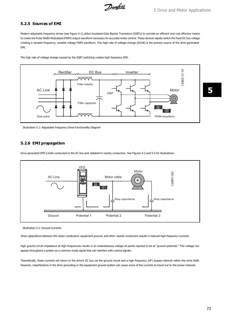
7/16/2019 1. D & E Frame.pdf
http://slidepdf.com/reader/full/1-d-e-framepdf 73/197
5.2.5 Sources of EMI
Modern adjustable frequency drives (see Figure 5-1) utilize Insulated-Gate Bipolar Transistors (IGBTs) to provide an efficient and cost effective means
to create the Pulse Width Modulated (PWM) output waveform necessary for accurate motor control. These devices rapidly switch the fixed DC bus voltage
creating a variable frequency, variable voltage PWM waveform. This high rate of voltage change [dV/dt] is the primary source of the drive generated
EMI.
The high rate of voltage change caused by the IGBT switching creates high frequency EMI.
1 3 0 B X 1 3 7 . 1 0
AC Line
Rectifier DC Bus Inverter
Motor
Filter reactor
IGBT
Filter capacitor
PWM waveformSine wave
Illustration 5.1: Adjustable Frequency Drive Functionality Diagram
5.2.6 EMI propagation
Drive generated EMI is both conducted to the AC line and radiated to nearby conductors. See Figures 5-2 and 5-3 for illustrations.
1 3 0 B X 1 3 8 . 1 1
elbacr otoMeniLC A
Ground Potential 1 Potential 2 Potential 3
VFD
Motor
Stray capacitance Stray capacitance
Illustration 5.2: Ground Currents
Stray capacitance between the motor conductors, equipment ground, and other nearby conductors results in induced high frequency currents.
High ground circuit impedance at high frequencies results in an instantaneous voltage at points reputed to be at “ground potential.” This voltage can
appear throughout a system as a common mode signal that can interfere with control signals.
Theoretically, these currents will return to the drive’s DC bus via the ground circuit and a high frequency (HF) bypass network within the drive itself.
However, imperfections in the drive grounding or the equipment ground system can cause some of the currents to travel out to the power network.
5 Drive and Motor Applications
73
5

7/16/2019 1. D & E Frame.pdf
http://slidepdf.com/reader/full/1-d-e-framepdf 74/197
1 3 0 B X 1 3 9 . 1 1
elbacr otoMeniLC A
VFDMotor
Stray capacitance
Signal wiring to BMS
Illustration 5.3: Signal Conductor Currents
Unprotected or poorly routed signal conductors located close to or in parallel to motor and AC line conductors are susceptible to EMI.
Signal conductors are especially vulnerable when they are run parallel to the power conductors for any distance. EMI coupled into these conductors can
affect either the drive or the interconnected control device. See Figure 5-4.
While these currents will tend to travel back to the drive, imperfections in the system will cause some current to flow in undesirable paths thus exposing
other locations to the EMI.
1 3 0 B X 1 4 0 . 1 1
elbacr otoMeniLC A
VFDMotor
Stray capacitance
AC Line
Illustration 5.4: Alternate Signal Conductor Currents
High frequency currents can be coupled into the AC line supplying the drive when the AC line conductors are located close to the motor cables.
5.2.7 Preventive measures
EMI related problems are more effectively alleviated during the design and installation phases rather then after the system is in service. Many of the steps
listed here can be implemented at a relatively low cost when compared to the cost to later identify and fix the problem in the f ield.
Grounding
The drive and motor should be solidly grounded to the equipment frame. A good high frequency connection is necessary to allow the high frequency
currents to return back to the drive rather than to travel thorough the power network. The ground connection will be ineffective if it has high impedance
to high frequency currents, therefore it should be as short and direct as practical. Flat braided cable has lower high frequency impedance than round
cable. Simply mounting the drive or motor onto a painted surface will not create an effective ground connection. In addition, running a separate ground
conductor directly between the drive and the driven motor is recommended.
Cable routing
Avoid routing motor wiring, AC line wiring, and signal wiring in parallel. If parallel routing is unavoidable, try to maintain a separation of 200mm (6 - 8
inches) between the cables or separate them with a grounded conductive partition. Avoid routing cables through free air.
5 Drive and Motor Applications
74
5
7/16/2019 1. D & E Frame.pdf
http://slidepdf.com/reader/full/1-d-e-framepdf 75/197
Signal cable selection
Signal cable selection. Single conductor 600 volt rated wires provide the least protection from EMI. Twisted-pair and shielded twist-pair cables are available
which are specifically designed to minimize the effects of EMI. While unshielded twisted-pair cables are often adequate, shielded twisted-pair cables
provide another degree of protection. The signal cable’s shield should be terminated in a manner that is appropriate for the connected equipment. Avoid
terminating the shield through a pigtail connection as this increases the high frequency impedance and spoils the effectiveness of the shield. Refer to
Section 1, Grounding Shielded Cables.
A simple alternative is to twist the existing single conductors to provide a balanced capacitive and inductive coupling thus canceling out differential-mode
interference. While not as effective as true twisted-pair cable, it can be implemented in the field using the materials on hand.
Motor cable selection
The management of the motor conductors has the greatest influence on the EMI characteristics of the system. These conductors should receive the
highest attention whenever EMI is a problem. Single conductor wires provide the least protection from EMI emissions. Often if these conductors are
routed separately from the signal and AC line wiring then no further consideration is needed. If the conductors are routed close to other susceptible
conductors, or if the system is suspected of causing EMI problems then alternate motor wiring methods should be considered.
Installing shielded power cable is the most effective means to alleviate EMI problems. The cable’s shield forces the noise current to flow directly back to
the drive before it gets back into the power network or takes other undesirable and unpredictable high frequency paths. Unlike most signal wiring, the
shielding on the motor cable should be terminated at both ends.
If shielded motor cable is not available, then 3 phase conductors plus ground in a conduit will provide some degree of protection. This technique will not
be as effective as shielded cable due to the unavoidable contact of the conduit with various points within the equipment.
Serial communications cable selectionThere are various serial communication interfaces and protocols on the market. Each of these recommends one or more specific types of twisted-pair,
shielded twisted-pair, or proprietary cables. Refer to the manufacturer’s documentation when selecting these cables. Similar recommendations apply to
serial communication cables as to other signal cables. Using twisted-pair cables and routing them away from power conductors is encouraged. While
shielded cable provides additional EMI protection, the shield capacitance may reduce the maximum allowable cable length at high data rates.
5.2.8 Proper EMC installation
Shown in the figure below is a correct installation with EMC considerations in mind. Although most installations will not follow all the recommended
practices the closer an installation resembles this example the better immunity the network will have against EMI. Should EMI problems arise in an
installation, refer to this example. Attempt to replicate this installation recommendation as closely as possible to alleviate such problems.
5 Drive and Motor Applications
75
5
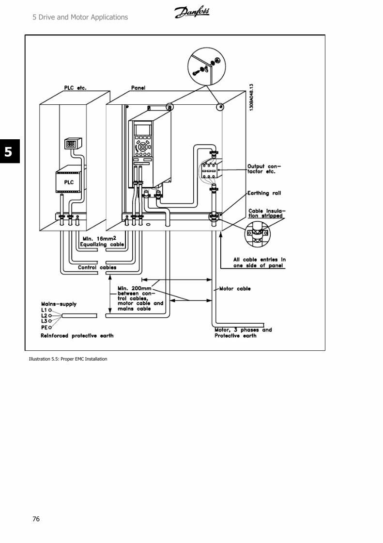
7/16/2019 1. D & E Frame.pdf
http://slidepdf.com/reader/full/1-d-e-framepdf 76/197
Illustration 5.5: Proper EMC Installation
5 Drive and Motor Applications
76
5

7/16/2019 1. D & E Frame.pdf
http://slidepdf.com/reader/full/1-d-e-framepdf 77/197
6 Test Procedures
6.1 Introduction
Touching electrical parts of drive may be fatal even after equipment has been disconnected from AC power. Wait 20 minutes for D-
frame sizes or 40 minutes for E-frame sizes after power has been removed before touching any internal components to ensure that
capacitors have fully discharged. See label on front of drive door for specific discharge time.
This section contains detailed procedures for testing VLT drives. Previous sections of this manual provide symptoms, alarms and other conditions which
require additional test procedures to further diagnose the drive. The results of these tests indicate the appropriate repair actions. Again, because the
drive monitors input and output signals, motor conditions, AC and DC power and other functions, the source of fault conditions may exist outside of the
drive itself. Testing described here will isolate many of these conditions as well. Sections 7 and 8, Disassembly and Assembly Instructions, describes
detailed procedures for removing and replacing drive components, as required (D- or E-sized drives, respectively).
Drive testing is divided into Static Tests , Dynamic Tests , and Initial Start Up or After Repair Drive Tests . Static tests are conducted without power applied
to the drive. Most drive problems can be diagnosed simply with these tests. Static tests are performed with little or no disassembly. The purpose of static
testing is to check for shorted power components. Perform these tests on any unit suspected of containing faulty power components prior to applyingpower.
For dynamic test procedures, main input power is required. All line powered devices and power supplies are energized at rated voltage.
Use extreme caution when conducting tests on a powered drive. Contact with powered components could result in electrical shock and
personal injury.
Dynamic tests are performed with power applied to the drive. Dynamic testing traces signal circuitry to isolate faulty components.
Both D-frame and E-frame size drives are covered here. Differences in the procedures are noted, as required. However, the Soft Charge and Rectifier
Circuit Test, Soft Charge Rectifier Test, and Fan Continuity Test sections are independent for D-frame and E-frame drives.
Replace any defective component and retest the drive with the new component before applying power to the drive as described in Initial Start Up or After
Repair Drive Tests .
6.1.1 Tools required for testing
Digital volt/ohm meter capable of reading real RMS
Analog volt meter
Oscilloscope
Clamp-on style ammeter
Signal test board p/n 176F8437
Test cable p/n 176F8439
6 Test Procedures
77
6

7/16/2019 1. D & E Frame.pdf
http://slidepdf.com/reader/full/1-d-e-framepdf 78/197
6.1.2 Signal test board
The signal test board can be used to test circuitry within the drive and provides easy access to test points. The test board plugs into connector MK104
on the power card. Its use is described in the procedures where called out. See Signal Test Board in Section 9, Special Test Equipment , for detailed pin
descriptions.
1 3 0 B X 6 6 . 1 0
Illustration 6.1: Signal Test Board
6.1.3 Test cables
The test cables bypass the main DC bus and supply DC voltage to the power card from the soft charge card. This provides voltage for testing the power
card without the drive circuitry being powered. The SCR shorting plug ensures that the SCRs do not fire. There are two cable types. For D-frame drives,
use the 3-pin cable; for E-frame drives, use the 2-pin cable (see Figure 6-2). The cable connects between the soft charge connector MK3 and the power
card connector MK105.
1 3 0 B X 6 4 . 1 0
Illustration 6.2: Test Cables and SCR Shorting Plug
6 Test Procedures
78
6

7/16/2019 1. D & E Frame.pdf
http://slidepdf.com/reader/full/1-d-e-framepdf 79/197
6.2 Static Test Procedures
All tests should be made with a meter capable of testing diodes. Use a digital volt/ohm meter (VOM) set on the diode scale or an analog ohmmeter set
on Rx100 scale. Before making any checks disconnect all input, motor and brake resistor connections.
Figure 6-3 Power Card PCA Connector Identification is provided as a reference for finding the appropriate connectors described in the test procedures in
this section. Some connectors are optional and not on all drive configurations.
NB!
For best troubleshooting results, it is recommended that static test procedures described in this section be performed in the order
presented.
Diode Drop
A diode drop reading will vary depending on the model of ohmmeter. Whatever the ohmmeter displays as a typical forward bias diode is defined as a
"diode drop" in these procedures. With a typical DVM, the voltage drop across most components will be around .300 to .500. The opposite reading is
referred to as infinity and most DMVs will display the value OL for overload.
1
2
34
5
6
7
8
9
10
11
12
13
14
15
16
130BX172.10
Illustration 6.3: Power Card, and Mounting Plate
380-480/500V: Yellow tape on Main SMPS transformer in upper right corner.
525-690V: White tape on Main SMPS transformer in upper right corner.
1 Power card PCA3 9 MK1062 Mounting plate 10 MK1003 MK110 11 MK1094 MK102 12 FK1025 MK104 13 MK112 terminals 1, 2, 36 MK105 14 MK112 terminals 4, 5, 67 MK107 15 Scaling card8 FK103 16 Scaling card standoff
6 Test Procedures
79
6
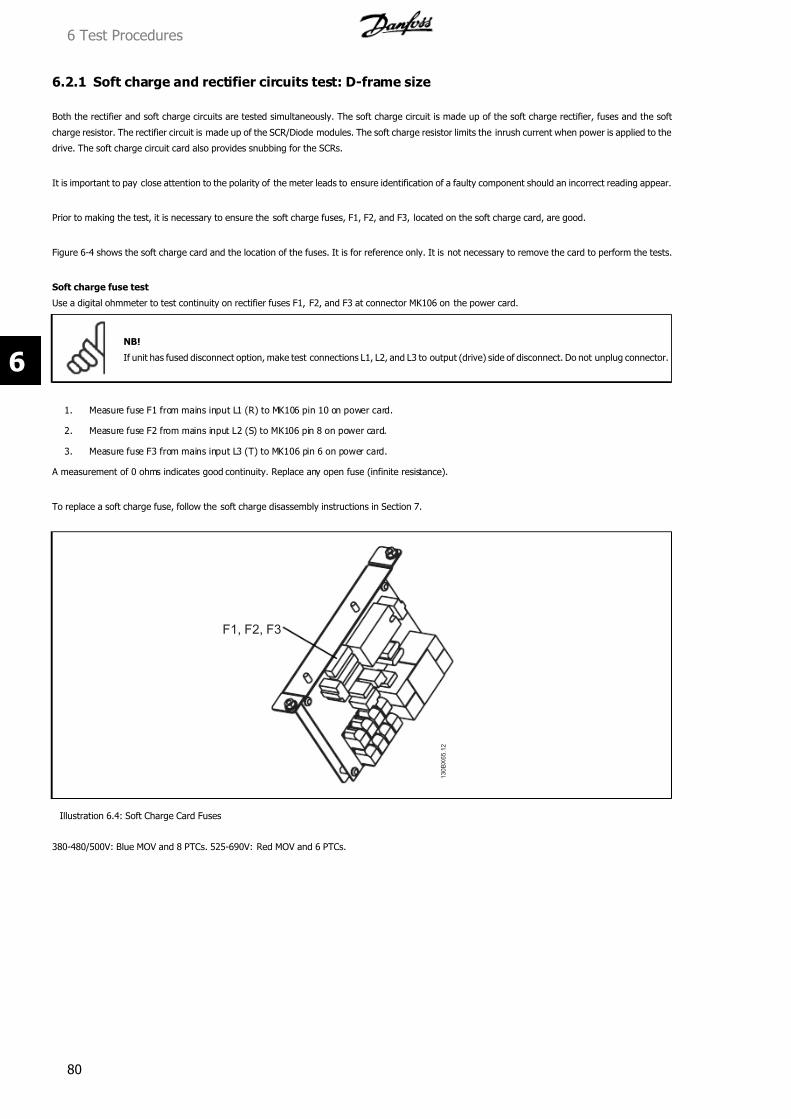
7/16/2019 1. D & E Frame.pdf
http://slidepdf.com/reader/full/1-d-e-framepdf 80/197
6.2.1 Soft charge and rectifier circuits test: D-frame size
Both the rectifier and soft charge circuits are tested simultaneously. The soft charge circuit is made up of the soft charge rectifier, fuses and the soft
charge resistor. The rectifier circuit is made up of the SCR/Diode modules. The soft charge resistor limits the inrush current when power is applied to the
drive. The soft charge circuit card also provides snubbing for the SCRs.
It is important to pay close attention to the polarity of the meter leads to ensure identification of a faulty component should an incorrect reading appear.
Prior to making the test, it is necessary to ensure the soft charge fuses, F1, F2, and F3, located on the soft charge card, are good.
Figure 6-4 shows the soft charge card and the location of the fuses. It is for reference only. It is not necessary to remove the card to perform the tests.
Soft charge fuse test
Use a digital ohmmeter to test continuity on rectifier fuses F1, F2, and F3 at connector MK106 on the power card.
NB!
If unit has fused disconnect option, make test connections L1, L2, and L3 to output (drive) side of disconnect. Do not unplug connector.
1. Measure fuse F1 from mains input L1 (R) to MK106 pin 10 on power card.
2. Measure fuse F2 from mains input L2 (S) to MK106 pin 8 on power card.
3. Measure fuse F3 from mains input L3 (T) to MK106 pin 6 on power card.
A measurement of 0 ohms indicates good continuity. Replace any open fuse (infinite resistance).
To replace a soft charge fuse, follow the soft charge disassembly instructions in Section 7.
1 3 0 B X 6 5 . 1
2
F1, F2, F3
Illustration 6.4: Soft Charge Card Fuses
380-480/500V: Blue MOV and 8 PTCs. 525-690V: Red MOV and 6 PTCs.
6 Test Procedures
80
6

7/16/2019 1. D & E Frame.pdf
http://slidepdf.com/reader/full/1-d-e-framepdf 81/197
Main rectifier circuit test part I
1. Connect positive (+) meter lead to positive (+) DC bus connector MK105 (A) on power card.
2. Connect negative (–) meter lead to terminals L1, L2, and L3 in turn.
Each reading should show infinity. The meter will start at a low value and slowly climb towards infinity due to capacitance within the drive being charged
by the meter.
Incorrect reading
With the Part I test connection, the SCRs in the SCR/Diode modules are reverse biased so they are blocking current flow. If a short circuit exists, it wouldbe possible that either the SCRs or the diodes in the soft charge rectifier are shorted. To isolate between SCRs or the soft charge rectifier, perform the
Soft Charge Rectifier Test.
Main rectifier circuit test part II
1. Reverse meter leads by connecting negative (–) meter lead to positive (+) DC bus connector MK105 (A) on power card.
2. Connect positive (+) meter lead to L1, L2, and L3 in turn. Each reading should show a diode drop.
Incorrect reading
With the Part II test connection, even though the SCRs in the SCR/Diode modules are forward biased by the meter, current will not flow through the
SCRs without providing a signal to their gates. The upper diodes in the soft charge rectifier are forward biased so the meter reads the voltage drop across
those diodes.
If an open reading were present, it would indicate the upper diodes in the soft charge rectifier are open. It could also indicate that one or more of the
soft charge fuses are open. It could further indicate that the soft charge resistor is open. To isolate between the three possibilities, perform the Soft
Charge Fuse Test and Soft Charge Rectifier Test.
A short circuit reading indicates either one or more of the upper soft charge rectifier diodes are shorted or the SCRs are shorted in the SCR/Diode module.
To isolate between SCRs or the soft charge rectifier, perform the Soft Charge Rectifier Test.
Main rectifier circuit test part III
1. Connect positive (+) meter lead to negative (-) DC bus connector MK105 (B) on power card.
2. Connect negative (–) meter lead to terminals L1, L2 and L3 in turn. Each reading should show a diode drop.
Incorrect reading With the Part III test connection, the diodes in the SCR/Diode modules are forward biased as well as the lower diodes in the soft
charge rectifier. The meter reads the diode drops. If a short circuit exists it would be possible that either the diodes in the SCR/Diode modules or the
lower diodes in the soft charge rectifier are shorted. To isolate between SCRs or the soft charge rectifier, perform the Soft Charge Rectifier Test.
Although an open reading is possible, it is unlikely since that indicates that both the diodes in the SCR/diode modules and the lower diodes in the soft
charge rectifier are open. Should that occur, replace both diodes.
Main rectifier circuit test part IV
1. Reverse meter leads by connecting negative (–) meter lead to negative (-) DC bus connector MK105 (B) on power card.
2. Connect positive (+) meter lead to L1, L2 and L3 in turn. Each reading should show infinity.
Each reading should show infinity. The meter will start at a low value and slowly climb toward infinity due to capacitance within the drive being charged
by the meter.
Incorrect reading
With the Part IV test connection, the diodes in the SCR/Diode modules are reversed biased as well as the lower diodes in the soft charge rectifier. If a
short circuit exists it would be possible that either the diodes in the SCR/Diode modules or the lower diodes in the soft charge rectifier are shorted. Toisolate between SCRs or the soft charge rectifier, perform the Soft Charge Rectifier Test, 6.2.2.
6.2.2 Soft charge rectifier test: D-frame size
Testing the soft charge rectifier requires access to the soft charge card connectors. It requires removing the control card and power card mounting plate.
Refer to removal instructions for soft charge card in Section 7.
Do not remove the soft charge card completely or unplug any connectors not called out. Doing so will break the continuity path of these measurements
and may result in a false interpretation of a failure. Although an open reading is possible, it is unlikely since that indicates that both the diodes in the
SCR/diode modules and the lower diodes in the soft charge rectifier are open. Should that occur, replace both diodes.
6 Test Procedures
81
6
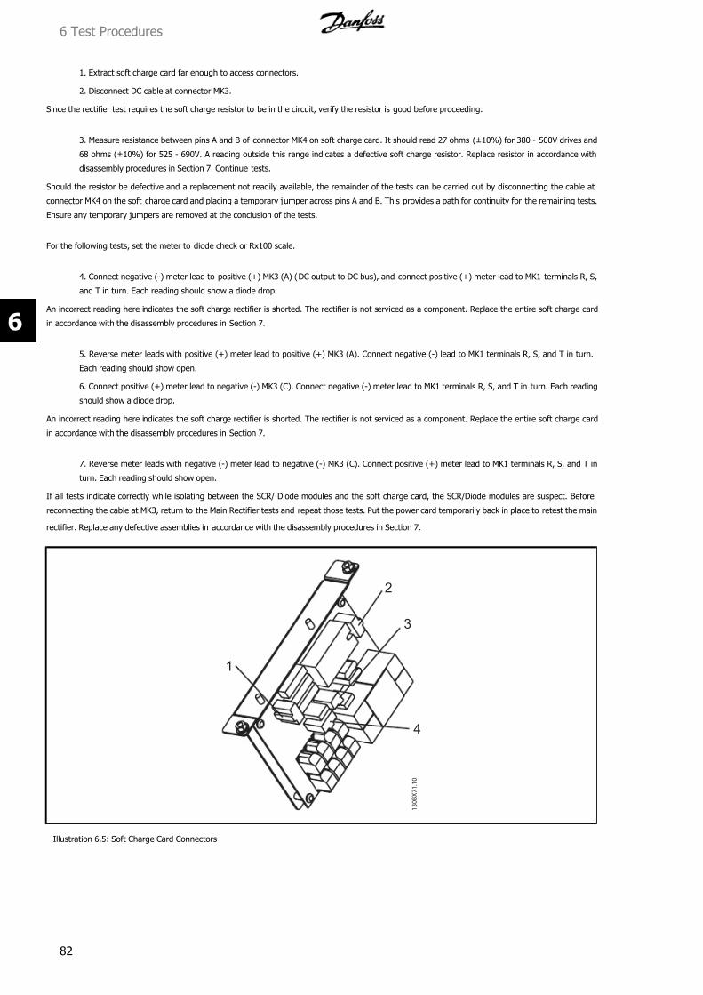
7/16/2019 1. D & E Frame.pdf
http://slidepdf.com/reader/full/1-d-e-framepdf 82/197
1. Extract soft charge card far enough to access connectors.
2. Disconnect DC cable at connector MK3.
Since the rectifier test requires the soft charge resistor to be in the circuit, verify the resistor is good before proceeding.
3. Measure resistance between pins A and B of connector MK4 on soft charge card. It should read 27 ohms (±10%) for 380 - 500V drives and
68 ohms (±10%) for 525 - 690V. A reading outside this range indicates a defective soft charge resistor. Replace resistor in accordance with
disassembly procedures in Section 7. Continue tests.
Should the resistor be defective and a replacement not readily available, the remainder of the tests can be carried out by disconnecting the cable at
connector MK4 on the soft charge card and placing a temporary jumper across pins A and B. This provides a path for continuity for the remaining tests.
Ensure any temporary jumpers are removed at the conclusion of the tests.
For the following tests, set the meter to diode check or Rx100 scale.
4. Connect negative (-) meter lead to positive (+) MK3 (A) (DC output to DC bus), and connect positive (+) meter lead to MK1 terminals R, S,
and T in turn. Each reading should show a diode drop.
An incorrect reading here indicates the soft charge rectifier is shorted. The rectifier is not serviced as a component. Replace the entire soft charge card
in accordance with the disassembly procedures in Section 7.
5. Reverse meter leads with positive (+) meter lead to positive (+) MK3 (A). Connect negative (-) lead to MK1 terminals R, S, and T in turn.
Each reading should show open.
6. Connect positive (+) meter lead to negative (-) MK3 (C). Connect negative (-) meter lead to MK1 terminals R, S, and T in turn. Each reading
should show a diode drop.
An incorrect reading here indicates the soft charge rectifier is shorted. The rectifier is not serviced as a component. Replace the entire soft charge card
in accordance with the disassembly procedures in Section 7.
7. Reverse meter leads with negative (-) meter lead to negative (-) MK3 (C). Connect positive (+) meter lead to MK1 terminals R, S, and T in
turn. Each reading should show open.
If all tests indicate correctly while isolating between the SCR/ Diode modules and the soft charge card, the SCR/Diode modules are suspect. Before
reconnecting the cable at MK3, return to the Main Rectifier tests and repeat those tests. Put the power card temporarily back in place to retest the main
rectifier. Replace any defective assemblies in accordance with the disassembly procedures in Section 7.
1 3 0 B X 7 1 . 1 0
1
2
3
4
Illustration 6.5: Soft Charge Card Connectors
6 Test Procedures
82
6
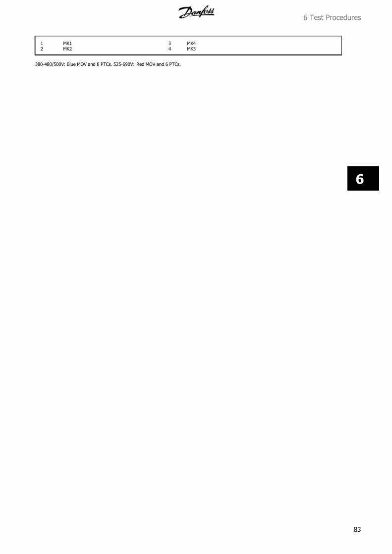
7/16/2019 1. D & E Frame.pdf
http://slidepdf.com/reader/full/1-d-e-framepdf 83/197
1 MK1 3 MK42 MK2 4 MK3
380-480/500V: Blue MOV and 8 PTCs. 525-690V: Red MOV and 6 PTCs.
6 Test Procedures
83
6
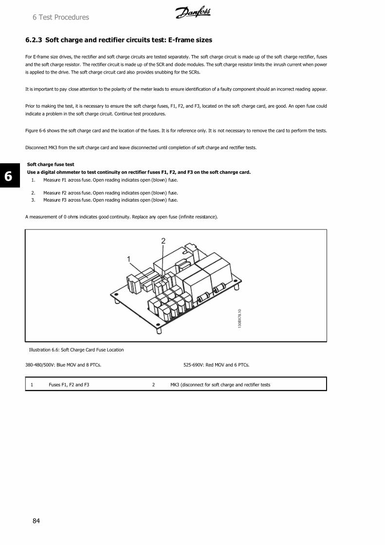
7/16/2019 1. D & E Frame.pdf
http://slidepdf.com/reader/full/1-d-e-framepdf 84/197
6.2.3 Soft charge and rectifier circuits test: E-frame sizes
For E-frame size drives, the rectifier and soft charge circuits are tested separately. The soft charge circuit is made up of the soft charge rectifier, fuses
and the soft charge resistor. The rectifier circuit is made up of the SCR and diode modules. The soft charge resistor limits the inrush current when power
is applied to the drive. The soft charge circuit card also provides snubbing for the SCRs.
It is important to pay close attention to the polarity of the meter leads to ensure identification of a faulty component should an incorrect reading appear.
Prior to making the test, it is necessary to ensure the soft charge fuses, F1, F2, and F3, located on the soft charge card, are good. An open fuse could
indicate a problem in the soft charge circuit. Continue test procedures.
Figure 6-6 shows the soft charge card and the location of the fuses. It is for reference only. It is not necessary to remove the card to perform the tests.
Disconnect MK3 from the soft charge card and leave disconnected until completion of soft charge and rectifier tests.
Soft charge fuse test
Use a digital ohmmeter to test continuity on rectifier fuses F1, F2, and F3 on the soft chanrge card.
1. Measure F1 across fuse. Open reading indicates open (blown) fuse.
2. Measure F2 across fuse. Open reading indicates open (blown) fuse.
3. Measure F3 across fuse. Open reading indicates open (blown) fuse.
A measurement of 0 ohms indicates good continuity. Replace any open fuse (infinite resistance).
1 3 0 B X 7 8 . 1 0
1
2
Illustration 6.6: Soft Charge Card Fuse Location
380-480/500V: Blue MOV and 8 PTCs. 525-690V: Red MOV and 6 PTCs.
1 Fuses F1, F2 and F3 2 MK3 (disconnect for soft charge and rectifier tests
6 Test Procedures
84
6

7/16/2019 1. D & E Frame.pdf
http://slidepdf.com/reader/full/1-d-e-framepdf 85/197
Main rectifier circuit test E-frames part I
1. Connect positive (+) meter lead to positive (+) DC bus connector MK105 (A) on power card.
2. Connect negative (–) meter lead to terminals L1, L2, and L3 in turn. If a disconnect option is used, measure on top side of fuses.
Each reading should show infinity. The meter will start at a low value and slowly climb towards infinity due to capacitance within the drive being charged
by the meter.
Incorrect reading
With the Part I test connection, the SCR modules are blocking current flow. A short indicates a shorted SCR module.
Main rectifier circuit test E-frames part II
1. Reverse meter leads by connecting negative (–) meter lead to positive (+) DC bus connector MK105 (A) on power card.
2. Connect positive (+) meter lead to L1, L2, and L3 in turn. Each reading should show open.
Incorrect reading
With the Part II test connection, the SCR modules are blocking current flow. A short indicates a shorted SCR module.
Main rectifier circuit test E-frames part III
1. Connect positive (+) meter lead to negative (-) DC bus connector MK105 (B) on power card.
2. Connect negative (–) meter lead to terminals L1, L2 and L3 in turn. Each reading should show a diode drop.
Incorrect reading
With the Part III test connection, the diodes in the main rectifier diode modules are forward biased. The meter reads the diode drops. If a short circuit
or an open circuit exists, the diode module is damaged.
Main rectifier circuit test E-frames part IV
1. Reverse meter leads by connecting negative (–) meter lead to negative (-) DC bus connector MK105 (B) on power card.
2. Connect positive (+) meter lead to L1, L2 and L3 in turn. Each reading should show infinity.
Each reading should show infinity. The meter will start at a low value and slowly climb toward infinity due to capacitance within the drive being charged
by the meter.
Incorrect reading
With the Part IV test connection, the diodes in the main diode modules are reversed biased. If a short circuit exists, the diode module is damaged.
Continue to Soft Charge Rectifier Tests: E-frames.
6 Test Procedures
85
6
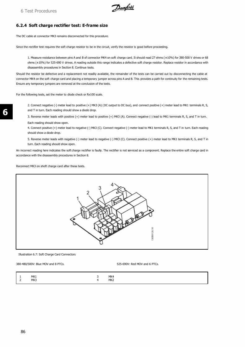
7/16/2019 1. D & E Frame.pdf
http://slidepdf.com/reader/full/1-d-e-framepdf 86/197
6.2.4 Soft charge rectifier test: E-frame size
The DC cable at connector MK3 remains disconnected for this procedure.
Since the rectifier test requires the soft charge resistor to be in the circuit, verify the resistor is good before proceeding.
1. Measure resistance between pins A and B of connector MK4 on soft charge card. It should read 27 ohms (±10%) for 380-500 V drives or 68
ohms (±10%) for 525-690 V drives. A reading outside this range indicates a defective soft charge resistor. Replace resistor in accordance with
disassembly procedures in Section 8. Continue tests.
Should the resistor be defective and a replacement not readily available, the remainder of the tests can be carried out by disconnecting the cable at
connector MK4 on the soft charge card and placing a temporary jumper across pins A and B. This provides a path for continuity for the remaining tests.
Ensure any temporary jumpers are removed at the conclusion of the tests.
For the following tests, set the meter to diode check or Rx100 scale.
2. Connect negative (-) meter lead to positive (+) MK3 (A) (DC output to DC bus), and connect positive (+) meter lead to MK1 terminals R, S,
and T in turn. Each reading should show a diode drop.
3. Reverse meter leads with positive (+) meter lead to positive (+) MK3 (A). Connect negative (-) lead to MK1 terminals R, S, and T in turn.
Each reading should show open.
4. Connect positive (+) meter lead to negative (-) MK3 (C). Connect negative (-) meter lead to MK1 terminals R, S, and T in turn. Each reading
should show a diode drop.
5. Reverse meter leads with negative (-) meter lead to negative (-) MK3 (C). Connect positive (+) meter lead to MK1 terminals R, S, and T in
turn. Each reading should show open.
An incorrect reading here indicates the soft charge rectifier is faulty. The rectifier is not serviced as a component. Replace the entire soft charge card in
accordance with the disassembly procedures in Section 8.
Reconnect MK3 on shoft charge card after these tests.
1 3 0 B X 1 2 0 . 1 0
1
23
4
Illustration 6.7: Soft Charge Card Connectors
380-480/500V: Blue MOV and 8 PTCs. 525-690V: Red MOV and 6 PTCs.
1 MK1 3 MK42 MK3 4 MK2
6 Test Procedures
86
6

7/16/2019 1. D & E Frame.pdf
http://slidepdf.com/reader/full/1-d-e-framepdf 87/197
6.2.5 Inverter section tests
The inverter section is primarily made up of the IGBTs used for switching the DC bus voltage to create the output to the motor. IGBTs are grouped into
modules comprised of six IGBTs. Depending on the size of the unit, either one, two, or three IGBT modules are present. The drive also has 3 snubber
capacitors on each IGBT module.
Disconnect motor leads when testing inverter section. With leads connected, a short circuit in one phase will read in all phases, making
isolation difficult.
Before starting tests, ensure that meter is set to diode scale. If removed previously, reinstall the soft charge card and power cards. Do not disconnect
the cable to connector MK105 on the power card since the path for continuity would be broken.
Inverter test part
1. Connect positive (+) meter lead to (+) positive DC bus connector MK105 (A) on power card.
2. Connect negative (–) meter lead to terminals U, V, and W in turn.
Each reading should show infinity. The meter will start at a low value and slowly climb toward infinity due to capacitance within the drive being charged
by the meter.
Inverter test part II
1. Reverse the meter leads by connecting negative (–) meter lead to positive (+) DC bus connector MK105 (A) on power card.
2. Connect positive (+) meter lead to U, V, and W in turn. Each reading should show a diode drop.
Incorrect reading
An incorrect reading in any inverter test indicates a failed IGBT module. Replace the IGBT module in accordance with the disassembly instructions in
Section 7or 8. It is further recommended for units with two IGBT modules that both modules be replaced even if the second module tests correctly.
Inverter test part III
1. Connect positive (+) meter lead to the negative (-) DC bus connector MK105 (B) on power card.
2. Connect negative (–) meter lead to terminals U, V, and W in turn. Each reading should show a diode drop.
Inverter test part IV
1. Reverse the meter leads by connecting negative (–) meter lead to negative (-) DC bus connector MK105 (B) on power card.
2. Connect positive (+) meter lead to U, V, and W in turn.
Each reading should show infinity. The meter will start at a low value and slowly climb toward infinity due to capacitance within the drive being charged
by the meter.
Incorrect reading
An incorrect reading in any inverter test indicates a failed IGBT module. Replace the IGBT module in accordance with the disassembly instructions in
Section 7 or 8. It is further recommended for units with two IGBT modules that both modules be replaced even if the second module tests correctly.
Indications of a failure in this circuit
IGBT failures may be caused by the drive being exposed to repeated short circuits or ground faults, or by extended drive operation outside of its normal
operating parameters. Following an IGBT failure, it is important to verify the gate drive signals are present and of the correct waveform. See the dynamic
test section on checking IGBT gate drive signals.
Gate resistor test
Mounted to each IGBT module is an IGBT gate resistor board containing, among other components, the gate resistors for the IGBT transistors. Based on
the nature of the failure, a defective IGBT can produce good readings from the previous tests. In nearly all cases, the failure of an IGBT will result in the
failure of the gate resistors.
Located on the gate drive card near each of the gate signal leads is a 3 pin test connector. These are labeled MK 250, 350, 450, 550, 650, 750, and, if
the drive is equipped with a brake option, 850.
For the sake of clarity, refer to the 3 pins as one, two, and three, reading left to right. Pins 1 and 2 of each connector are in parallel with the gate drive
signal sent to the IGBTs. Pin 1 is the signal and Pin 2 is common.
1. With ohm meter, measure pins 1 and 2 of each test connector. Reading should indicate 7.8K ohms for D1/D3 Frames, 3.9K ohms for D2/D4
Frames, and 2.6K ohms for E1/E2 frames.
6 Test Procedures
87
6
7/16/2019 1. D & E Frame.pdf
http://slidepdf.com/reader/full/1-d-e-framepdf 88/197
Incorrect reading
An incorrect reading indicates that either the gate signal wires are not connected from the gate drive card to the gate resistor board or the gate resistors
are defective. Connect gate signal wires, or if the resistors are defective, the entire IGBT module assembly requires replacement. Replace the IGBT module
in accordance with the disassembly procedures in Section 7 or 8.
6.2.6 Brake IGBT test
This test can only be carried out on units equipped with a dynamic brake option. If a brake resistor is connected to terminals 81 and 82, disconnect it
before proceeding. Use an ohm meter set on diode check or Rx100 scale.
Brake IGBT test part I
1. Connect positive (+) meter lead to brake resistor terminal R+ (82).
2. Connect negative (-) meter lead to brake resistor terminal R- (81).
The reading should indicate infinity. The meter may start out at a value and climb toward infinity as capacitance is charged within the drive.
Brake IGBT test part II
1. Connect positive (+) meter lead to brake resistor terminal R- (81).
2. Connect negative (-) meter lead to brake resistor terminal R+ (82).
The reading should indicate a diode drop.
Brake IGBT test part III
1. Connect positive (+) meter lead to brake resistor terminal R- (81).
2. Connect negative (-) meter lead to negative (-) DC bus connector MK105 (B) on the power card.
The reading should indicate infinity. The meter may start out at a value and climb toward infinity as capacitance is charged within the drive.
Incorrect reading
An incorrect reading on any of the above tests indicates that the brake IGBT is defective. Replace the brake IGBT in accordance with the disassembly
procedures in Section 7 or 8.
The failure of any IGBT may also lead to a failure of the gate drive circuit supplying that device. Following the replacement of an IGBT, always ensure
the gate drive signals are tested in accordance with the procedures in the dynamic test section.
6.2.7 Intermediate section tests
The intermediate section of the drive is made up of the DC bus capacitors, the DC coils, and the balance circuit for the capacitors.
1. Test for short circuits with ohmmeter set on Rx100 scale or, for a digital meter, select diode.
2. Measure across positive (+) DC terminal (A) and negative (–) DC terminal (B) on connector MK105 on power card. Observe meter polarity.
3. Meter will start out with low ohms and then move towards infinity as meter charges capacitors.
4. Reverse meter leads on connector MK105 on power card.
5. Meter will peg at zero while capacitors are discharged by meter. Meter then begins moving slowly toward two diode drops as meter charges
capacitors in reverse direction. Although test does not ensure capacitors are fully functional, it ensures no short circuits exist in intermediate
circuit.
Incorrect reading
A short circuit could be caused by a short in the soft charge, rectifier, or inverter section. Be sure that the test for these circuits have already been
performed successfully. A failure in one of these sections could be read in the intermediate section since they are all across the DC bus.
If a short circuit is present, and the unit is equipped with a brake, perform the brake IGBT test next.
The only other likely cause would be a defective capacitor within the capacitor bank.
There is not an effective test of the capacitor bank when it is fully assembled. Although unlikely that a failure within the capacitor bank would not be
indicated by a physically damaged capacitor, if suspect, the entire capacitor bank must be replaced. Replace the capacitor bank in accordance with the
disassembly procedures in Section 7 or 8.
6 Test Procedures
88
6

7/16/2019 1. D & E Frame.pdf
http://slidepdf.com/reader/full/1-d-e-framepdf 89/197
6.2.8 Heatsink temperature sensor test
The temperature sensor is an NTC (negative temperature coefficient) device. As a result, high resistance means low temperature. As temperature de-
creases, resistance increases. Each IGBT module has a temperature sensor mounted internally. The sensor is wired from the IGBT module to the gate
driver card connector MK100. For drives with two IGBTs, the sensor on the right module is used. For drives with three IGBT modules, the center module
is used.
On the gate drive card, the resistance signal is converted to a frequency
signal. The frequency signal is sent to the power card for processing. The
temperature data is used to regulate fan speed and to monitor for over
and under temperature conditions.
1. Use ohmmeter set to read ohms.
2. Unplug connector MK100 on gate drive card (see Figure 6-15)
and measure resistance across cable leads.
The relationship between temperature and resistance is nonlinear. At 25°C, the resistance will be approximately 5k Ohms. At 0°C, the resistance will be
approximately 13.7k Ohms. At 60°C, the resistance will be approximately 1.5k Ohms. The higher the temperature, the lower the resistance.
6 Test Procedures
89
6
7/16/2019 1. D & E Frame.pdf
http://slidepdf.com/reader/full/1-d-e-framepdf 90/197
6.2.9 Fan continuity tests: D-frame size
Make all continuity checks using an ohmmeter set to Rx1 scale. Digital or analog ohmmeter can be used.
To aid in making the measurements, unplug the connector CN2 from its mate. CN2 terminals correspond to the terminal numbers labeled on the trans-
former.
Checking continuity of connections
For the following tests, read the plug end of connector CN2 that is not connected to the transformer.
1. Measure from L3 (T) to CN2 terminal 1. A reading of <1ohm should be indicated.
2. Measure from L2 (S) to CN2 terminal 3. A reading of <1 ohm should be indicated.
3. Measure from CN2 terminal 2 to terminal 12 of power card connector MK107. A reading of <1 ohm should be indicated.
Incorrect reading
An incorrect reading would indicate a faulty cable connection. Replace the cable assembly.
Ohm test of transformer (380 - 500V)
For the following tests, read the plug end of connector CN2 that is connected to the transformer.
1. Measure between CN2 terminals 1 and 3. Approximately 15 ohms should be read.
2. Measure between CN2 terminals 1 and 2. Approximately 12 ohms should be read.
3. Measure between CN2 terminals 2 and 3. Approximately 4 ohms should be read.
Incorrect reading
An incorrect reading would indicate a defective fan transformer. Replace the fan transformer.
When finished, be sure to reconnect CN2.
Ohm test of transformer (525 - 690V)
For the following tests, read the plug end of connector CN2 that is connected to the transformer.
1. Measure between CN2 terminals 1 and 3. Approximately 20 ohms should be read.
2. Measure between CN2 terminals 1 and 2. Approximately 8 ohms should be read.
3. Measure between CN2 terminals 2 and 3. Approximately 12 ohms should be read.
Incorrect reading
An incorrect reading would indicate a defective fan transformer. Replace the fan transformer.
When finished, be sure to reconnect CN2.
Ohm test of fans
1. Measure between terminals 11 and 13 of power card connector MK107. A reading of 20 ohms should be indicated.
2. Disconnect spade connectors from door fan and repeat measurement. A reading of 21 ohms should be indicated.
3. Read terminals of door fan with wires disconnected. A reading of 400 ohms should be indicated.
4. Reconnect wires to door fan.
Incorrect reading
An incorrect reading of one or both of the fans indicates a defective fan. Replace the defective fan.
6 Test Procedures
90
6
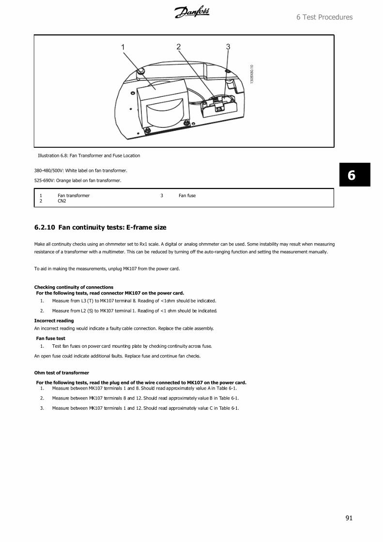
7/16/2019 1. D & E Frame.pdf
http://slidepdf.com/reader/full/1-d-e-framepdf 91/197
1 3 0 B X 8 0 . 1 0
1 2 3
Illustration 6.8: Fan Transformer and Fuse Location
380-480/500V: White label on fan transformer.
525-690V: Orange label on fan transformer.
1 Fan transformer 3 Fan fuse2 CN2
6.2.10 Fan continuity tests: E-frame size
Make all continuity checks using an ohmmeter set to Rx1 scale. A digital or analog ohmmeter can be used. Some instability may result when measuring
resistance of a transformer with a multimeter. This can be reduced by turning off the auto-ranging function and setting the measurement manually.
To aid in making the measurements, unplug MK107 from the power card.
Checking continuity of connections
For the following tests, read connector MK107 on the power card.
1. Measure from L3 (T) to MK107 terminal 8. Reading of <1ohm should be indicated.
2. Measure from L2 (S) to MK107 terminal 1. Reading of <1 ohm should be indicated.
Incorrect reading
An incorrect reading would indicate a faulty cable connection. Replace the cable assembly.
Fan fuse test
1. Test fan fuses on power card mounting plate by checking continuity across fuse.
An open fuse could indicate additional faults. Replace fuse and continue fan checks.
Ohm test of transformer
For the following tests, read the plug end of the wire connected to MK107 on the power card.
1. Measure between MK107 terminals 1 and 8. Should read approximately value A in Table 6-1.
2. Measure between MK107 terminals 8 and 12. Should read approximately value B in Table 6-1.
3. Measure between MK107 terminals 1 and 12. Should read approximately value C in Table 6-1.
6 Test Procedures
91
6

7/16/2019 1. D & E Frame.pdf
http://slidepdf.com/reader/full/1-d-e-framepdf 92/197
AC Voltage Drive Resistance (in Ohms) Heatsink Fan Fan Inductor
FC102 FC202 FC302 A B C D
380-500 P315 P315 P250 15 12 4 21 no380-500 P355 P355 P315 4 3 1 4 yes380-500 P400 P400 P355 4 3 1 4 yes380-500 P450 P450 P400 4 3 1 4 yes525-690 P400 P400 P355 20 8 12 21 no525-690 P500 P500 P400 20 8 12 21 no525-690 P560 P560 P500 7.4 3.6 3.2 4 yes525-690 P630 P630 P560 7.4 3.6 3.2 4 yes
Table 6.1: Fan transformer resistance
Incorrect reading
An incorrect reading would indicate a defective fan transformer. Replace the fan transformer.
When finished reconnect MK107.
Ohm test of fans
1. Measure between terminals 3 and 5 of power card connector MK107. Should read approximately value D in Table 6-1.
Incorrect reading
For fans without an inductor, replace the fan. For drives with a fan and inductor, isolate the fault between the fan and the
inductor as follows.
1a Disconnect CN3 and measure resistance between pins 1 and 2 on fan side of connector. Reading should be approx 4 ohms. If incorrect,
replace fan.
1b Disconnect CN4 and CN5. Measure resistance across inductor. Reading should be less than 1 ohm. If incorrect, replace inductor.
2. Measure between terminals 11 and 13 of power card connector MK107. For units with one top mounted fan, a reading of 400 ohms is expected.
For units with two door mounted fans, a reading of 200 ohms is expected.
Incorrect reading
For units with one top mounted fan, replace the fan. For units with two door mounted fans, isolate the faulty fan as follows.
a. Disconnect wiring from fan terminals.
b. Read across fan terminals on each fan. A reading of 400 ohms is expected. Replace any defective fans.
Illustration 6.9: Fan and DC Bus Fuse Locations
1 Power card 4 Mounting plate2 DC bus fuse 5 MK1073 Fan fuse
6 Test Procedures
92
6

7/16/2019 1. D & E Frame.pdf
http://slidepdf.com/reader/full/1-d-e-framepdf 93/197
6.3 Dynamic Test Procedures
Refer to terminal locations in Figure 6-10 for performing dynamic test procedures.
NB!
Test procedures in this section are numbered for reference only. Tests do not need to be performed in this order. Perform tests only
as necessary.
Never disconnect input cabling to drive with power applied due to danger of severe injury or death.
Take all necessary safety precautions for system start up prior to applying power to drive.
1 3 0 B X 7 9 . 1 0
1
2
34
Illustration 6.10: Drive Power Terminals (D-size Frames)
1 Main 3-phase AC power to drive 3 Brake resistor connection2 DC bus/loadsharing connections 4 3-phase output to motor
6 Test Procedures
93
6
7/16/2019 1. D & E Frame.pdf
http://slidepdf.com/reader/full/1-d-e-framepdf 94/197
6.3.1 No display test
A drive with no display can be the result of several causes. Verify first that there is no display whatsoever. A single character in the display or a dot in
the upper corner of the display indicates a communication error and is typically caused by an option card not properly installed. Under this condition the
green power-on LED is illuminated.
If the LCD display is completely dark and the green power-on LED is not lit, proceed with the following tests.
First test for proper input voltage.
6.3.2 Input voltage test
1. Apply power to drive.
2. Use DVM to measure input line voltage between drive input terminals in turn:
L1 to L2
L1 to L3
L2 to L3
For 380 - 500 V drives, all measurements must be within the range of 342 to 550 VAC. Readings of less than 342 VAC indicate problems with the input
AC line voltage. For 525 - 690 V drives, all measurements must be within the range of 446 to 759 VAC. Readings of less than 446 VAC indicate problems
with the input AC line voltage.
In addition to the actual voltage reading, the balance of the voltage between the phases is also important. The drive can operate within specifications as
long as the phase imbalance is not more than 3%.
Danfoss calculates line imbalance per an IEC specification.
Imbalance = 0.67 X (Vmax – Vmin) / Vavg
For example, if three phase readings were taken and the results were 500 VAC, 478.5 VAC, and 478.5 VAC; then 500 VAC is Vmax, 478.5 VAC is Vmin,
and 485.7 VAC is Vavg, resulting in an imbalance of 3%.
Although the drive can operate at higher line imbalances, the lifetime of components, such as DC bus capacitors, will be shortened.
Incorrect reading
An incorrect reading here requires that the main supply be investigated further. Typical items to check would be:
Open (blown) input fuses or tripped circuit breakers
Open disconnects or line side contactors
Problems with the power distribution system
6 Test Procedures
94
6

7/16/2019 1. D & E Frame.pdf
http://slidepdf.com/reader/full/1-d-e-framepdf 95/197
Open (blown) input fuses or tripped circuit breakers usually indicate a more serious problem. Prior to replacing fuses or resetting
breakers, perform static tests described in section 6.2.
If the Input Voltage Test was successful check for voltage to the control card.
6.3.3 Basic control card voltage test
1. Measure control voltage at terminal 12 with respect to terminal 20. Meter should read between 21 and 27 VDC.
An incorrect reading here could indicate the supply is being loaded down by a fault in the customer connections. Unplug the terminal strip and repeat
the test. If this test is successful then continue. Remember to check out the customer connections. If still unsuccessful proceed to the Switch Mode Power
Supply (SMPS) test.
2. Measure 10 V DC control voltage at terminal 50 with respect to terminal 55. Meter should read between 9.2 and 11.2 VDC.
An incorrect reading here could indicate the supply is being loaded down by a fault in the customer connections. Unplug the terminal strip and repeat
the test. If this test is successful than continue. Remember to check out the customer connections. If still unsuccessful proceed to the SMPS test.
A correct reading of both control card voltages would indicate the LCP or the control card is defective. Replace the LCP with a known good one. If the
problem persists replace the control card in accordance with the disassembly procedures in Section 7 or 8.
6.3.4 Switch mode power supply (SMPS) test
The SMPS derives its power from the DC bus. The first indication that the DC bus is charged is the DC bus charge indicator light located on the power
card being lit. This LED however can be lit at a voltage still to low to enable the power supplies.
First test for the presence of the DC bus.
1. Using a voltmeter, read DC bus voltage at power card connector MK105 (A) with respect to MK105 (B). Meter should indicate approximately
1.35 x AC input voltage to drive.
2. If voltage is correct proceed to set 3. If voltage is present but out of range, proceed to DC Under Voltage test. If voltage is at zero, proceed to
Zero DC Bus Voltage test.
3. Test remaining power supplies. Insert signal test board into power card connector MK104
4. Connect negative (-) meter lead to terminal 4 (common) of signal board. With positive (+) meter lead check the following terminals on signal
board.
Terminal Supply Voltage Range
11 +18V 16.5 to 19.5 VDC12 -18V -16.5 to -19.5 VDC23 +24V 23 to 25 VDC
24 +5V 4.75 to 5.25 VDC
In addition, the signal test board contains three LED indicators that indicate the presence of voltage as follows:
Red LED +/- 18VDC supplies present
Yellow LED +24VDC supply present
Green LED +5VDC supply present
The lack of any one of these power supplies indicates the low voltage supplies on the power card are defective. This assumes of course that the proper
DC bus voltage was read at power card connector MK105 (A) and (B). Replace the power card in accordance with the disassembly procedures in Section
7 or 8.
6 Test Procedures
95
6
7/16/2019 1. D & E Frame.pdf
http://slidepdf.com/reader/full/1-d-e-framepdf 96/197
6.3.5 Zero DC bus voltage test
If no voltage is present at power card connector MK105 (A) and (B), check the condition of the DC power supply fuse. The fuse is located on the power
card mounting plate next to the power card. It can be tested without disassembling the unit.
1. Remove power to drive and ensure DC bus is fully discharged by measuring voltage at power card connector MK105 (A) with respect to MK105
(B).
If DC power supply fuse is open (blown), it is not possible to detect the presence of bus voltage at these terminals. If uncertain, wait
20 minutes for D-frame sizes or 40 minutes for E-frame sizes to allow DC bus to fully discharge. See label on front of drive door for
specific discharge time.
.
2. With ohmmeter set on diode scale or Rx100, measure from power card connector MK105 (A) to any bus bars coming from DC inductor. Bus
bars are visible at lower edge and beneath power card mounting bracket. Depending on bus bar read, look for a diode drop or complete short.
In either case this indicates a fuse is in the circuit providing a path for continuity. An open reading indicates open fuse.
If the fuse is open, it indicates a failure of the power supplies on the power card. The power card and fuse require replacement. If the fuse checks good,
there may be a problem with the soft charge circuitry. Proceed to the static checks of the soft charge and rectifier circuits earlier in this section.
6.3.6 DC under voltage test
The initial charge of the DC bus is accomplished by the soft charge circuit. If the DC bus voltage is below normal it would indicate that either the line
voltage is out of tolerance or the soft charge circuit is restricting the DC bus from charging. Conduct the input voltage test (6.3.2) to ensure the line
voltage is correct.
If excessive input power cycling has occurred, the PTC resistors on the soft charge card may be restricting the bus from charging. If this is the case,
expect to read a DC bus voltage in the area of 50 VDC.
1. Check DC bus voltage by reading power card connector MK105 (A) with respect to MK105 (B). If verified, remove power from drive and allow
it to cool for approximately 20 minutes.
2. Reapply power to drive after 20 minutes and recheck DC bus voltage. If voltage remains, a short circuit may exist within the intermediate circuit
preventing it from charging. Proceed to static checks (6.2) earlier in this section.
6.3.7 Input phase imbalance test
Theoretically, the current drawn on all three input phases should be equal. Some imbalance may be seen, however, due to variations in the phase to
phase input voltage and, to some degree, single phase loads within the drive itself.
A current measurement of each phase will reveal the balanced condition of the line. To obtain an accurate reading, it will be necessary for the drive to
run at its rated load or not less than 40% load.
1. Perform input voltage test prior to checking current in accordance with procedure. Voltage imbalances will automatically result in a corresponding
current imbalance.
2. Apply power to drive and place it in run.
3. Using a clamp-on amp meter (analog preferred), read current on each of three input lines at L1(R), L2(S), and L3(T).
Typically, the current should not vary from phase to phase by more than 5%. Should a greater current variation exist, it would indicate a possible problem
with the main supply to the drive or a problem within the drive itself.
One way to determine if the mains supply is at fault is to swap two of the incoming phases. This assumes that two phases read one current while the
third is more than 5% different. If all three phases are different from one another, swap the phase with the highest current with the phase with the
lowest current.
4. Remove power to drive.
6 Test Procedures
96
6
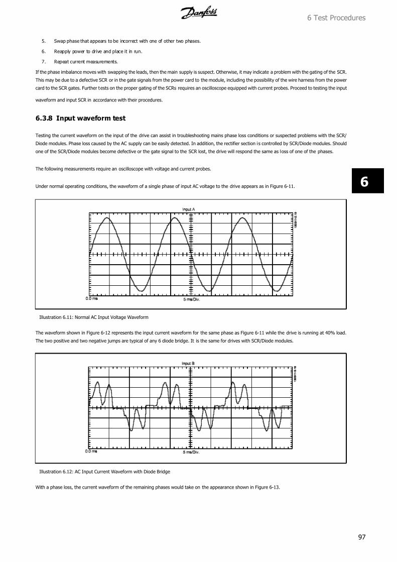
7/16/2019 1. D & E Frame.pdf
http://slidepdf.com/reader/full/1-d-e-framepdf 97/197
5. Swap phase that appears to be incorrect with one of other two phases.
6. Reapply power to drive and place it in run.
7. Repeat current measurements.
If the phase imbalance moves with swapping the leads, then the main supply is suspect. Otherwise, it may indicate a problem with the gating of the SCR.
This may be due to a defective SCR or in the gate signals from the power card to the module, including the possibility of the wire harness from the power
card to the SCR gates. Further tests on the proper gating of the SCRs requires an oscilloscope equipped with current probes. Proceed to testing the input
waveform and input SCR in accordance with their procedures. 6.3.8 Input waveform test
Testing the current waveform on the input of the drive can assist in troubleshooting mains phase loss conditions or suspected problems with the SCR/
Diode modules. Phase loss caused by the AC supply can be easily detected. In addition, the rectifier section is controlled by SCR/Diode modules. Should
one of the SCR/Diode modules become defective or the gate signal to the SCR lost, the drive will respond the same as loss of one of the phases.
The following measurements require an oscilloscope with voltage and current probes.
Under normal operating conditions, the waveform of a single phase of input AC voltage to the drive appears as in Figure 6-11.
Illustration 6.11: Normal AC Input Voltage Waveform
The waveform shown in Figure 6-12 represents the input current waveform for the same phase as Figure 6-11 while the drive is running at 40% load.
The two positive and two negative jumps are typical of any 6 diode bridge. It is the same for drives with SCR/Diode modules.
Illustration 6.12: AC Input Current Waveform with Diode Bridge
With a phase loss, the current waveform of the remaining phases would take on the appearance shown in Figure 6-13.
6 Test Procedures
97
6
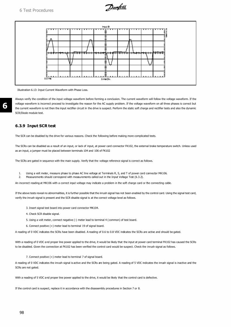
7/16/2019 1. D & E Frame.pdf
http://slidepdf.com/reader/full/1-d-e-framepdf 98/197
Illustration 6.13: Input Current Waveform with Phase Loss.
Always verify the condition of the input voltage waveform before forming a conclusion. The current waveform will follow the voltage waveform. If the
voltage waveform is incorrect proceed to investigate the reason for the AC supply problem. If the voltage waveform on all three phases is correct but
the current waveform is not then the input rectifier circuit in the drive is suspect. Perform the static soft charge and rectifier tests and also the dynamic
SCR/Diode module test.
6.3.9 Input SCR test
The SCR can be disabled by the drive for various reasons. Check the following before making more complicated tests.
The SCRs can be disabled as a result of an input, or lack of input, at power card connector FK102, the external brake temperature switch. Unless used
as an input, a jumper must be placed between terminals 104 and 106 of FK102
The SCRs are gated in sequence with the main supply. Verify that the voltage reference signal is correct as follows.
1. Using a volt meter, measure phase to phase AC line voltage at Terminals R, S, and T of power card connector MK106.
2. Measurements should correspond with measurements called out in the Input Voltage Test (6.3.2).
An incorrect reading at MK106 with a correct input voltage may indicate a problem in the soft charge card or the connecting cable.
If the above tests reveal no abnormalities, it is further possible that the inrush signal has not been enabled by the control card. Using the signal test card,
verify the inrush signal is present and the SCR disable signal is at the correct voltage level as follows.
3. Insert signal test board into power card connector MK104.
4. Check SCR disable signal.
5. Using a volt meter, connect negative (-) meter lead to terminal 4 (common) of test board.
6. Connect positive (+) meter lead to terminal 19 of signal board.
A reading of 0 VDC indicates the SCRs have been disabled. A reading of 0.6 to 0.8 VDC indicates the SCRs are active and should be gated.
With a reading of 0 VDC and proper line power applied to the drive, it would be likely that the input at power card terminal FK102 has caused the SCRs
to be disabled. Given the connection at FK102 has been verified the control card would be suspect. Check the inrush signal as follows.
7. Connect positive (+) meter lead to terminal 7 of signal board.
A reading of 0 VDC indicates the inrush signal is active and the SCRs are being gated. A reading of 5 VDC indicates the inrush signal is inactive and the
SCRs are not gated.
With a reading of 5 VDC and proper line power applied to the drive, it would be likely that the control card is defective.
If the control card is suspect, replace it in accordance with the disassembly procedures in Section 7 or 8.
6 Test Procedures
98
6
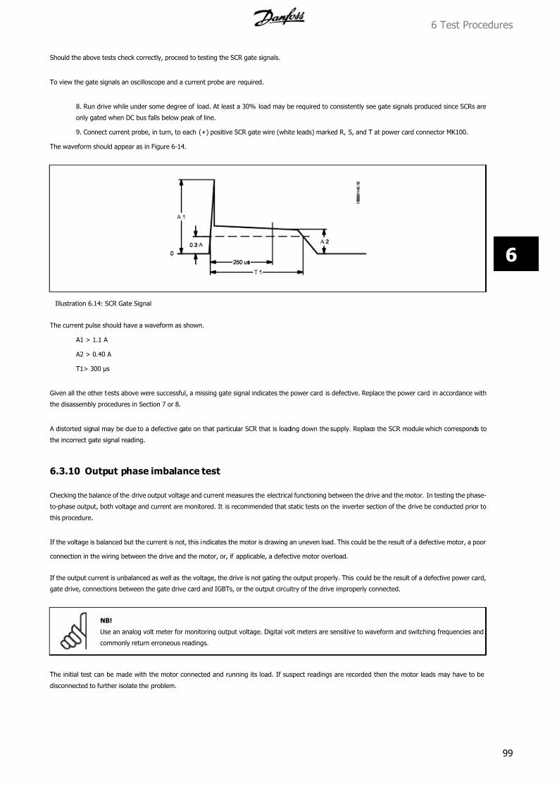
7/16/2019 1. D & E Frame.pdf
http://slidepdf.com/reader/full/1-d-e-framepdf 99/197
Should the above tests check correctly, proceed to testing the SCR gate signals.
To view the gate signals an oscilloscope and a current probe are required.
8. Run drive while under some degree of load. At least a 30% load may be required to consistently see gate signals produced since SCRs are
only gated when DC bus falls below peak of line.
9. Connect current probe, in turn, to each (+) positive SCR gate wire (white leads) marked R, S, and T at power card connector MK100.
The waveform should appear as in Figure 6-14.
Illustration 6.14: SCR Gate Signal
The current pulse should have a waveform as shown.
A1 > 1.1 A
A2 > 0.40 A
T1> 300 μs
Given all the other tests above were successful, a missing gate signal indicates the power card is defective. Replace the power card in accordance with
the disassembly procedures in Section 7 or 8.
A distorted signal may be due to a defective gate on that particular SCR that is loading down the supply. Replace the SCR module which corresponds to
the incorrect gate signal reading.
6.3.10 Output phase imbalance test
Checking the balance of the drive output voltage and current measures the electrical functioning between the drive and the motor. In testing the phase-
to-phase output, both voltage and current are monitored. It is recommended that static tests on the inverter section of the drive be conducted prior to
this procedure.
If the voltage is balanced but the current is not, this indicates the motor is drawing an uneven load. This could be the result of a defective motor, a poor
connection in the wiring between the drive and the motor, or, if applicable, a defective motor overload.
If the output current is unbalanced as well as the voltage, the drive is not gating the output properly. This could be the result of a defective power card,
gate drive, connections between the gate drive card and IGBTs, or the output circuitry of the drive improperly connected.
NB!
Use an analog volt meter for monitoring output voltage. Digital volt meters are sensitive to waveform and switching frequencies and
commonly return erroneous readings.
The initial test can be made with the motor connected and running its load. If suspect readings are recorded then the motor leads may have to be
disconnected to further isolate the problem.
6 Test Procedures
99
6
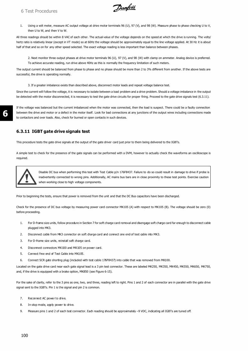
7/16/2019 1. D & E Frame.pdf
http://slidepdf.com/reader/full/1-d-e-framepdf 100/197
1. Using a volt meter, measure AC output voltage at drive motor terminals 96 (U), 97 (V), and 98 (W). Measure phase to phase checking U to V,
then U to W, and then V to W.
All three readings should be within 8 VAC of each other. The actual value of the voltage depends on the speed at which the drive is running. The volts/
hertz ratio is relatively linear (except in VT mode) so at 60Hz the voltage should be approximately equal to the line voltage applied. At 30 Hz it is about
half of that and so on for any other speed selected. The exact voltage reading is less important than balance between phases.
2. Next monitor three output phases at drive motor terminals 96 (U), 97 (V), and 98 (W) with clamp on ammeter. Analog device is preferred.
To achieve accurate reading, run drive above 40Hz as this is normally the frequency limitation of such meters.
The output current should be balanced from phase to phase and no phase should be more than 2 to 3% different from another. If the above tests are
successful, the drive is operating normally.
3. If a greater imbalance exists than described above, disconnect motor leads and repeat voltage balance test.
Since the current will follow the voltage, it is necessary to isolate between a load problem and a drive problem. Should a voltage imbalance in the output
be detected with the motor disconnected, it is necessary to test the gate drive circuits for proper firing. Proceed to the gate drive signals test (6.3.11).
If the voltage was balanced but the current imbalanced when the motor was connected, then the load is suspect. There could be a faulty connection
between the drive and motor or a defect in the motor itself. Look for bad connections at any junctions of the output wires including connections made
to contactors and over loads. Also, check for burned or open contacts in such devices.
6.3.11 IGBT gate drive signals test
This procedure tests the gate drive signals at the output of the gate driver card just prior to them being delivered to the IGBTs.
A simple test to check for the presence of the gate signals can be performed with a DVM, however to actually check the waveforms an oscilloscope is
required.
Disable DC bus when performing this test with Test Cable p/n 176F8437. Failure to do so could result in damage to drive if probe is
inadvertently connected to wrong pins. Additionally, AC mains bus bars are in close proximity to these test points. Exercise caution
when working close to high voltage components.
Prior to beginning the tests, ensure that power is removed from the unit and that the DC Bus capacitors have been discharged.
Check for the presence of DC bus voltage by measuring power card connector MK105 (A) with respect to MK105 (B). The voltage should be zero (0)
before proceeding.
1. For D-frame size units, follow procedure in Section 7 for soft charge card removal and disengage soft charge card far enough to disconnect cable
plugged into MK3.
2. Disconnect cable from MK3 connector on soft charge card and connect one end of test cable into MK3.
3. For D-frame size units, reinstall soft charge card.
4. Disconnect connectors MK100 and MK105 on power card.
5. Connect free end of Test Cable into MK105.
6. Connect SCR gate shorting plug (included with test cable 176F8437) into cable that was removed from MK100.
Located on the gate drive card near each gate signal lead is a 3 pin test connector. These are labeled MK250, MK350, MK450, MK550, MK650, MK750,
and, if the drive is equipped with a brake option, MK850 (see Figure 6-15).
For the sake of clarity, refer to the 3 pins as one, two, and three, reading left to right. Pins 1 and 2 of each connector are in parallel with the gate drive
signal sent to the IGBTs. Pin 1 is the signal and pin 2 is common.
7. Reconnect AC power to drive.
8. In stop mode, apply power to drive.
9. Measure pins 1 and 2 of each test connector. Each reading should be approximately –9 VDC, indicating all IGBTs are tuned off.
6 Test Procedures
100
6

7/16/2019 1. D & E Frame.pdf
http://slidepdf.com/reader/full/1-d-e-framepdf 101/197
10. Apply run command to drive and 30 Hz reference.
11. If using a DVM, measure pins 1 and 2 of each connector. Waveform to IGBTs is a square wave that goes positive to 14 VDC and negative to -9
VDC. Average voltage read by DVM should be 2.2 to 2.5 VDC.
6 Test Procedures
101
6
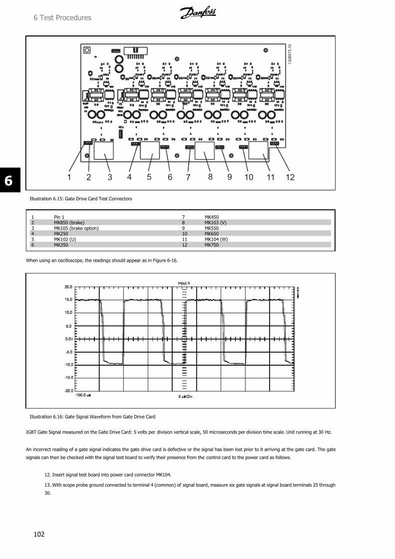
7/16/2019 1. D & E Frame.pdf
http://slidepdf.com/reader/full/1-d-e-framepdf 102/197
1 3 0 B X 7 5 . 1 0
1 2 3 4 5 6 7 8 9 10 11 12
Illustration 6.15: Gate Drive Card Test Connectors
1 Pin 1 7 MK4502 MK850 (brake) 8 MK103 (V)3 MK105 (brake option) 9 MK5504 MK250 10 MK6505 MK102 (U) 11 MK104 (W)6 MK350 12 MK750
When using an oscilloscope, the readings should appear as in Figure 6-16.
Illustration 6.16: Gate Signal Waveform from Gate Drive Card
IGBT Gate Signal measured on the Gate Drive Card: 5 volts per division vertical scale, 50 microseconds per division time scale. Unit running at 30 Hz.
An incorrect reading of a gate signal indicates the gate drive card is defective or the signal has been lost prior to it arriving at the gate card. The gate
signals can then be checked with the signal test board to verify their presence from the control card to the power card as follows.
12. Insert signal test board into power card connector MK104.
13. With scope probe ground connected to terminal 4 (common) of signal board, measure six gate signals at signal board terminals 25 through
30.
6 Test Procedures
102
6
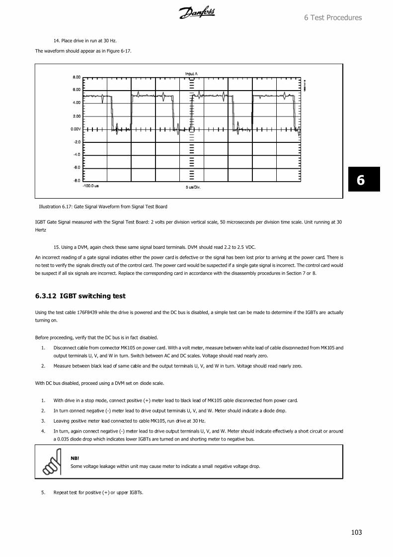
7/16/2019 1. D & E Frame.pdf
http://slidepdf.com/reader/full/1-d-e-framepdf 103/197
14. Place drive in run at 30 Hz.
The waveform should appear as in Figure 6-17.
Illustration 6.17: Gate Signal Waveform from Signal Test Board
IGBT Gate Signal measured with the Signal Test Board: 2 volts per division vertical scale, 50 microseconds per division time scale. Unit running at 30
Hertz
15. Using a DVM, again check these same signal board terminals. DVM should read 2.2 to 2.5 VDC.
An incorrect reading of a gate signal indicates either the power card is defective or the signal has been lost prior to arriving at the power card. There is
no test to verify the signals directly out of the control card. The power card would be suspected if a single gate signal is incorrect. The control card would
be suspect if all six signals are incorrect. Replace the corresponding card in accordance with the disassembly procedures in Section 7 or 8.
6.3.12 IGBT switching test
Using the test cable 176F8439 while the drive is powered and the DC bus is disabled, a simple test can be made to determine if the IGBTs are actually
turning on.
Before proceeding, verify that the DC bus is in fact disabled.
1. Disconnect cable from connector MK105 on power card. With a volt meter, measure between white lead of cable disconnected from MK105 and
output terminals U, V, and W in turn. Switch between AC and DC scales. Voltage should read nearly zero.
2. Measure between black lead of same cable and the output terminals U, V, and W in turn. Voltage should read nearly zero.
With DC bus disabled, proceed using a DVM set on diode scale.
1. With drive in a stop mode, connect positive (+) meter lead to black lead of MK105 cable disconnected from power card.
2. In turn connect negative (-) meter lead to drive output terminals U, V, and W. Meter should indicate a diode drop.
3. Leaving positive meter lead connected to cable MK105, run drive at 30 Hz.
4. In turn, again connect negative (-) meter lead to drive output terminals U, V, and W. Meter should indicate effectively a short circuit or around
a 0.035 diode drop which indicates lower IGBTs are turned on and shorting meter to negative bus.
NB!
Some voltage leakage within unit may cause meter to indicate a small negative voltage drop.
5. Repeat test for positive (+) or upper IGBTs.
6 Test Procedures
103
6
7/16/2019 1. D & E Frame.pdf
http://slidepdf.com/reader/full/1-d-e-framepdf 104/197
6. With drive in a stop mode, connect negative (-) meter lead to white lead of MK105 cable disconnected from power card.
7. In turn, connect positive (+) meter lead to drive output terminals U, V, and W. Meter should indicate a diode drop.
8. Leaving negative meter lead connected to cable MK105, run drive at 30 Hz.
9. In turn, again connect positive (+) meter lead to drive output terminals U, V, and W. Meter should indicate effectively a short circuit or around
a 0.035 diode drop which indicates upper IGBTs are turned on and shorting meter to positive bus.
NB!
Some voltage leakage within unit may cause meter to indicate a small negative voltage drop.
Incorrect Reading
An incorrect reading indicates some of the IGBTs are not turning on. Replace the IGBT module in accordance with the disassembly instructions in Section
7 or 8.
6.3.13 Brake IGBT test
Use the signal test board to test the operation of the dynamic brake IGBT and gate drive circuitry. The following procedure can be used to force the brake
circuit to activate for testing.
1. Connect signal test board to connector MK104 on control card.
2. Set voltage test switch labeled Over V to ON position.
3. Turn potentiometer on test board until brake circuit activates. This causes brake IGBT to turn on and off at approximately 1.2 KHz. Duty cycle
(pulse width) increases as potentiometer is increased.
4. Measure with oscilloscope or DVM at terminal 13. Terminal 13 represents gate signal to brake IGBT. This should be 4.04 VDC when brake is
OFF and drop to zero when brake is ON.
5. Measure with oscilloscope or DVM at terminal 14. Terminal 14 is a logic level (5V) signal representing voltage across brake IGBT. This should
measure 5.1 VDC when brake is OFF and drop to zero when brake is ON.
Incorrect Reading
If the signal on terminal 13 is not correct, first check that the drive is correctly programmed for dynamic braking (parameter 2-10). If the programming
is correct, replace the control card in accordance with procedures in Section 7 or 8.
If the signal on terminal 13 is correct but the signal on terminal 14 is not, the brake IGBT gate signal must be checked to determine whether the fault
lies in the IGBT or the gate driver card. See Gate Drive Signal Tests.
6.3.14 Current sensors test
The current sensors are Hall effect devices that send a signal proportional to the actual output current waveform to the power card. The current scaling
card, attached to the power card, scales the signals from the current sensors to the proper level for monitoring and processing motor control data. A
defective current sensor can cause erroneous ground faults and over current trips. In such instances, the fault will usually only occur at higher loads. If
the incorrect current scaling card is installed, the current signals will be improperly scaled. This could cause erroneous over current trips. If the current
scaling card is not installed, the drive will trip.
A couple of simple checks can be made to determine the status of the sensors.
1. Apply power to drive.
2. Ensure that motor check, pre-magnetizing, DC hold, DC brake, or other parameter setups are disabled that create a holding torque while at zero
speed. Current displayed will exceed 1 to 2 amps if such parameters are not disabled.
3. Run drive with a zero speed reference. Note output current reading in display. Display should indicate approximately 1 to 2 amps.
If the current is greater than 1 to 2 amps and a current producing parameter is not active, the test will need to be made again with the motor leads
disconnected.
6 Test Procedures
104
6

7/16/2019 1. D & E Frame.pdf
http://slidepdf.com/reader/full/1-d-e-framepdf 105/197
4. Remove power from drive. Monitor DC bus voltage at power card connector MK105 (A) and (B) to ensure bus is fully discharged.
5. Remove output motor leads from terminals U, V, and W.
6. Apply power to drive.
7. Run drive with a zero speed reference. Note output current reading in display. Display should indicate less than 1 amp.
If an incorrect reading was obtained from the above tests, further tests of the current feedback signals are required using the signal test board.
Testing current feedback with the signal test board.
8. Remove power to drive. Ensure DC bus is fully discharged.
9. Install signal test board into power card connector MK104.
10. Using a DVM, measure resistance between terminals 1 and 4, 2 and 4, and 3 and 4 of signal test board. Resistance should be the same for
all three readings. Table 6-2 shows approximate resistance readings based on drive power and voltage rating. Note that values listed are values
at the current scaling card. When measuring with signal test board, actual reading may be higher due to meter lead resistance. Absence of
resistance indicates a missing scaling card.
11. Reapply power to drive.
12. Using a DVM, connect negative (-) meter lead to terminal 4 (common) of signal test board.
13. Run drive with a zero speed reference.
14. In turn measure AC voltage at terminals 1, 2, and 3 of signal test board. These terminals correspond with current sensor outputs U, V, and
W, respectively. Expect a reading near zero volts but no greater than 15mv.
If the control card parameters are setup to provide holding torque while at zero speed, the current displayed will be greater than expected. To make this
test disable such parameters.
The current sensor feedback signal at this point in the circuit will read approximately 400mv at 100% drive load so any reading above 15mv while the
drive is at zero speed has a negative effect on the way the drive interprets the feedback signal.
A reading of greater than 15mv suggests that the corresponding current sensor be replaced. See the disassembly instructions in Section 7 or 8.
6 Test Procedures
105
6

7/16/2019 1. D & E Frame.pdf
http://slidepdf.com/reader/full/1-d-e-framepdf 106/197
Voltage (AC) FC102 FC202 FC302 CT Resistance (Ohms)
380-500 P110 P110 P90 4.5
380-500 P132 P132 P110 3.8
380-500 P160 P160 P132 3.1
380-500 P200 P200 P160 2.6
380-500 P250 P250 P200 5.1
380-500 P315 P315 P250 4.2
380-500 P355 P355 P315 2.6
380-500 P400 P400 P355 2.6
380-500 P450 P450 P400 2.3
525-690 P45k P45k P37K 5.9
525-690 P55k P55k P45k 5.9
525-690 P75k P75k P55k 5.9
525-690 P90k P90k P75k 5.9
525-690 P110 P110 P90k 5.9
525-690 P132 P132 P110 5.9
525-690 P160 P160 P132 4.5
525-690 P200 P200 P160 3.1
525-690 P250 P250 P200 3.1
525-690 P315 P315 P250 2.6
525-690 P400 P400 P315 5.1
525-690 P450 P450 P355 4.5
525-690 P500 P500 P400 4.5
525-690 P560 P560 P500 3.8
525-690 P630 P630 P560 2.6
Table 6.2: Scaling Card Resistance Values
6.3.15 Fan tests
The fan control circuit is made up of the fan transformer and the control circuitry located on the power card along with control signals for ON, OFF, andspeed control from the control card. Since the fans do not necessarily run at all times, see the description of cooling fans operation under sequence of
operation in Section 3.3.5.
Supply voltage
Supply voltage for the fans is from the soft charge card to power card connector MK106. First verify the supply voltage is present as
follows.
1. With a voltmeter, measure AC phase to phase voltage at R, S, and T of power card connector MK106. It should equal main supply voltage applied
to drive.
2. If voltage is not present, ensure proper line voltage is applied to drive. Conduct Input Voltage test (6.3.2).
3. If line voltage is present at input of drive but not at MK106 of power card, conduct static test of soft charge fuses (6.2.1).
4. If voltage is present at MK106, check voltage at fan transformer read from connector CN2 located near transformer. With a volt meter, read AC
voltage at CN2 pins 1 and 3. Voltage should correspond to main AC line voltage applied to drive.
5. If voltage is not present, ensure jumpers are in place at power card connector FK103. Otherwise connect an external source of power to terminal
FK103 for fan supply voltage.
If the jumpers are in place or an auxiliary supply is connected and powered but no voltage is present at the fan transformer connector CN2, the power
card is likely defective. Replace the power card in accordance with the disassembly instructions in Section 7 or 8.
Transformer output
If the appropriate voltage is present at CN2 pins 1 and 3, next check the output of the transformer. Prior to making this test, ensure the fan transformer
fuse is good.
1. With a volt meter, measure AC voltage from CN2 terminal 1 to terminal 2. Voltage should equal 66% of main AC supply voltage (48% for drives
525-690 VAC) applied to drive (or that of auxiliary supply). If voltage is incorrect, replace fan transformer.
6 Test Procedures
106
6

7/16/2019 1. D & E Frame.pdf
http://slidepdf.com/reader/full/1-d-e-framepdf 107/197
2. If voltage is correct, check fan voltage being supplied to fans themselves. Voltage can be read at power card connector MK107 pins 8 and 11
with respect to pin 1. Voltage at pins 8 and 11 correspond to fan's commanded speed: 200 VAC for low speed and 230 VAC for high speed.
If the correct voltage is available but the fan is not running, that fan is defective. If no voltage is available, verify that the fans should be running. If so,
the power card is defective. Replace the fan or power card in accordance with the disassembly instructions in Section 7 or 8.
Fan control circuit
To verify that the fan control circuit is receiving appropriate commands from the control card, the signal test board can be used to verify those signals.
1. Remove power from drive and allow DC bus to fully discharge.
2. Install signal test board into power connector MK104.
3. Reapply power to drive.
4. Connect negative (-) meter lead of a voltmeter to signal board terminal 4 (common).
5. With positive (+) meter lead check signal at terminal 6 of signal board. Meter should read zero (0) volts with fans commanded to run, 5 VDC if
control card commands fans off.
6. Verify cooling fans sequence of operation to ensure they should be running. In addition, signal board contains a fan test switch. When switched
on fans should start and run at high speed.
The signals at terminals 5 and 10 of the signal board determine fan speed. See Section 9 for more on those signals. In addition, if a heat sink overtem-
perature trip has occurred, the fans will automatically be switched to high speed.
Given the fact that the fans should be running, if the signal at terminal 6 is correct and the fan test switch activates the fan, the control card is defective.
Otherwise the power card is defective. Replace the appropriate assembly in accordance with the disassembly instructions in Section 7 or 8.
6.3.16 Input terminal signal tests
The presence of signals on either the digital or analog input terminals of the drive can be verified on the drive display. Digital or analog input status can
be selected in the display using the [DISPLAY MODE] key and the [+] and [-] keys on the keypad.
6 Test Procedures
107
6
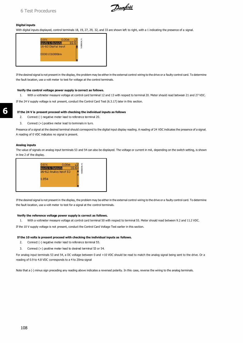
7/16/2019 1. D & E Frame.pdf
http://slidepdf.com/reader/full/1-d-e-framepdf 108/197
Digital inputs
With digital inputs displayed, control terminals 18, 19, 27, 29, 32, and 33 are shown left to right, with a 1 indicating the presence of a signal.
If the desired signal is not present in the display, the problem may be either in the external control wiring to the drive or a faulty control card. To determine
the fault location, use a volt meter to test for voltage at the control terminals.
Verify the control voltage power supply is correct as follows.
1. With a voltmeter measure voltage at control card terminal 12 and 13 with respect to terminal 20. Meter should read between 21 and 27 VDC.
If the 24 V supply voltage is not present, conduct the Control Card Test (6.3.17) later in this section.
If the 24 V is present proceed with checking the individual inputs as follows
2. Connect (-) negative meter lead to reference terminal 20.
3. Connect (+) positive meter lead to terminals in turn.
Presence of a signal at the desired terminal should correspond to the digital input display reading. A reading of 24 VDC indicates the presence of a signal.
A reading of 0 VDC indicates no signal is present.
Analog inputs
The value of signals on analog input terminals 53 and 54 can also be displayed. The voltage or current in mA, depending on the switch setting, is shown
in line 2 of the display.
If the desired signal is not present in the display, the problem may be either in the external control wiring to the drive or a faulty control card. To determine
the fault location, use a volt meter to test for a signal at the control terminals.
Verify the reference voltage power supply is correct as follows.
1. With a voltmeter measure voltage at control card terminal 50 with respect to terminal 55. Meter should read between 9.2 and 11.2 VDC.
If the 10 V supply voltage is not present, conduct the Control Card Voltage Test earlier in this section.
If the 10 volts is present proceed with checking the individual inputs as follows.
2. Connect (-) negative meter lead to reference terminal 55.
3. Connect (+) positive meter lead to desired terminal 53 or 54.
For analog input terminals 53 and 54, a DC voltage between 0 and +10 VDC should be read to match the analog signal being sent to the drive. Or a
reading of 0.9 to 4.8 VDC corresponds to a 4 to 20ma signal
Note that a (-) minus sign preceding any reading above indicates a reversed polarity. In this case, reverse the wiring to the analog terminals.
6 Test Procedures
108
6
7/16/2019 1. D & E Frame.pdf
http://slidepdf.com/reader/full/1-d-e-framepdf 109/197
6.4 Initial Start Up or After Repair Drive Tests
Following any repair to a drive or testing of a drive suspected of being faulty, the following procedure must be followed to ensure that all circuitry in the
drive is functioning properly before putting the unit into operation.
1. Perform visual inspection procedures as described in Table 4-1.
2. Perform static test procedures 6.2.1, 6.2.2 and 6.2.5 for D-frame size units or 6.2.3, 6.2.4 and 6.2.5 for E-frame size units to ensure drive is
safe to start.
3. Disconnect motor leads from output terminals (U, V, W) of drive.
4. Apply AC power to drive.
5. Give drive a run command and slowly increase reference (speed command) to approximately 40 Hz.
6. Using an analog volt meter or a DVM capable of measuring true RMS, measure phase-to-phase output voltage on all three phases: U to V, U to
W, V to W. Al l voltages must be balanced within 8 volts. If unbalanced voltage is measured, refer to Input Voltage Test (6.3.2).
7. Stop drive and remove input power. Allow 40 minutes for DC capacitors to fully discharge for E-frame size drives or 20 minutes for D-frame size
drives.
8. Reconnect motor leads to drive output terminals (U, V, W).
9. Reapply power and restart drive. Adjust motor speed to a nominal level.
10. Using a clamp-on style ammeter, measure output current on each output phase. All currents should be balanced. If unbalanced current is
measured, refer to Current Sensor Test (6.3.14).
6 Test Procedures
109
6

7/16/2019 1. D & E Frame.pdf
http://slidepdf.com/reader/full/1-d-e-framepdf 110/197
7 D-Frame Sizes Disassembly and AssemblyInstructions
110
7

7/16/2019 1. D & E Frame.pdf
http://slidepdf.com/reader/full/1-d-e-framepdf 111/197
7 D-Frame Sizes Disassembly and Assembly Instructions
7.1 Electrostatic Discharge (ESD)
Drives contain dangerous voltages when connected to line voltage. No disassembly should be attempted with power applied. Remove
power to drive and wait at least 20 minutes to let drive capacitors fully discharge. Only a competent technician should carry out service.
ELECTROSTATIC DISCHARGE (ESD)
Many electronic components within the adjustable frequency drive are sensitive to static electricity. Voltages so low that they cannot be felt, seen or
heard can reduce the life, affect performance, or completely destroy sensitive electronic components.
Use proper electrostatic discharge (ESD) procedures when servicing drive to prevent damage to sensitive components.
NB!
Frame size is used throughout this manual where ever procedures or components differ between drives based upon the unit's physical
size. Refer to tables in the Introduction Section to determine frame size definitions. See Section 8 for E-frame sizes disassembly and
assembly instructions.
7 D-Frame Sizes Disassembly and AssemblyInstructions
111
7

7/16/2019 1. D & E Frame.pdf
http://slidepdf.com/reader/full/1-d-e-framepdf 112/197
7.2 Instructions
7.2.1 Control Card and Control Card Mounting Plate
1. Open front panel door or remove front cover, depending on unit type.
2. (See Figure 7-1) Unplug LCP keypad ribbon cable (not shown) from control card or remove LCP, depending on unit type. LCP removes by hand.
3. Remove LCP cradle. LCP cradle removes by hand.
4. Remove any customer control wiring from control card terminal blocks.
5. Remove 4 screws (T20 Torx) securing control card mounting plate to control assembly support bracket.
6. Unplug ribbon cable from back of control card.
Reinstall in reverse order of this procedure. The red conductor on the ribbon cable between the control card and the power card should be on the bottom
of the connector. Tighten control card mounting plate screws to 1 Nm (8 in-lb).
7 D-Frame Sizes Disassembly and AssemblyInstructions
112
7

7/16/2019 1. D & E Frame.pdf
http://slidepdf.com/reader/full/1-d-e-framepdf 113/197
Illustration 7.1: Control Card Access
380-480/500V: Yellow tape on Main SMPS transformer in upper right cor-
ner.
525-690V: White tape on Main SMPS transformer in upper right corner.
1 Local control panel (LCP) (Step 2) 8 Power card PCA32 LCP cradle (Step 3) 9 MK102 ring lug connection3 C-option (if installed) 10 DC bus fuse4 Mounting screws (Step 5) 11 Control card mounting plate
5 Control assembly support bracket 12 Control card terminal block 6 Attaching hardware 13 Control card (under LCP)7 Power card mounting plate
7.2.2 Control Assembly Support Bracket
1. Remove control card mounting plate in accordance with procedure.
2. Remove 6 mounting nuts (10mm), see Figure 7-1.
3. Remove control assembly support bracket.
Reinstall in reverse order of this procedure. Tighten mounting screws to 4 Nm (35 in-lbs).
7 D-Frame Sizes Disassembly and AssemblyInstructions
113
7
7/16/2019 1. D & E Frame.pdf
http://slidepdf.com/reader/full/1-d-e-framepdf 114/197
7.2.3 Power Card
1. Remove control assembly support bracket in accordance with procedure.
2. Unplug power card connectors MK100, MK102, MK105, MK106, and MK107.
3. If customer connections are present, unplug connectors FK102, FK103, and MK112.
4. Remove 7 mounting screws (T25 Torx) from power card.
5. Remove power card from plastic standoff at top right of power card.
6. Remove current scaling card from power card by pushing in retaining clips on standoffs. KEEP THIS SCALING CARD TO REINSTALL ON ANY
REPLACEMENT POWER CARD. Scaling card controls signals operating with this specific VLT drive. Scaling card is not part of replacement power
card.
Reinstall in reverse order of this procedure. When installing the power card, ensure that the insulator sheet is installed behind the power card. Tighten
mounting screws to 2.5 Nm (20 in-lbs).
1
2
34
5
6
7
8
9
10
11
12
13
14
15
16
130BX172.10
Illustration 7.2: Power Card, and Mounting Plate
380-480/500V: Yellow tape on Main SMPS transformer in upper right cor-
ner.
525-690V: White tape on Main SMPS transformer in upper right corner.
1 Power card PCA3 9 MK1062 Mounting plate 10 MK1003 MK110 11 MK1094 MK102 12 FK1025 MK104 13 FK1016 MK105 14 FK1007 MK107 15 Current scaling card PCA48 FK103 16 Current scaling card standoff
7 D-Frame Sizes Disassembly and AssemblyInstructions
114
7
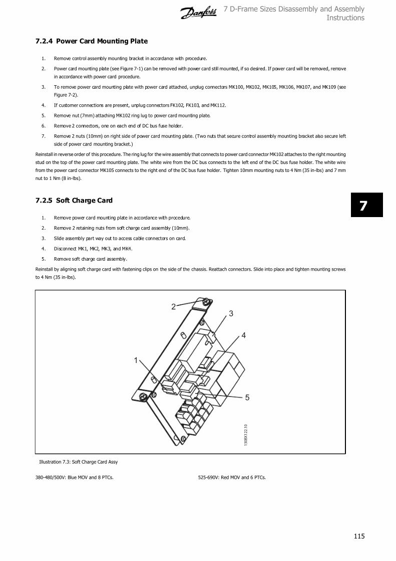
7/16/2019 1. D & E Frame.pdf
http://slidepdf.com/reader/full/1-d-e-framepdf 115/197
7.2.4 Power Card Mounting Plate
1. Remove control assembly mounting bracket in accordance with procedure.
2. Power card mounting plate (see Figure 7-1) can be removed with power card still mounted, if so desired. If power card will be removed, remove
in accordance with power card procedure.
3. To remove power card mounting plate with power card attached, unplug connectors MK100, MK102, MK105, MK106, MK107, and MK109 (see
Figure 7-2).
4. If customer connections are present, unplug connectors FK102, FK103, and MK112.
5. Remove nut (7mm) attaching MK102 ring lug to power card mounting plate.
6. Remove 2 connectors, one on each end of DC bus fuse holder.
7. Remove 2 nuts (10mm) on right side of power card mounting plate. (Two nuts that secure control assembly mounting bracket also secure left
side of power card mounting bracket.)
Reinstall in reverse order of this procedure. The ring lug for the wire assembly that connects to power card connector MK102 attaches to the right mounting
stud on the top of the power card mounting plate. The white wire from the DC bus connects to the left end of the DC bus fuse holder. The white wire
from the power card connector MK105 connects to the right end of the DC bus fuse holder. Tighten 10mm mounting nuts to 4 Nm (35 in-lbs) and 7 mm
nut to 1 Nm (8 in-lbs).
7.2.5 Soft Charge Card
1. Remove power card mounting plate in accordance with procedure.
2. Remove 2 retaining nuts from soft charge card assembly (10mm).
3. Slide assembly part way out to access cable connectors on card.
4. Disconnect MK1, MK2, MK3, and MK4.
5. Remove soft charge card assembly.
Reinstall by aligning soft charge card with fastening clips on the side of the chassis. Reattach connectors. Slide into place and tighten mounting screws
to 4 Nm (35 in-lbs).
1 3 0 B X 1 2 2 . 1 0
1
23
5
4
Illustration 7.3: Soft Charge Card Assy
380-480/500V: Blue MOV and 8 PTCs. 525-690V: Red MOV and 6 PTCs.
7 D-Frame Sizes Disassembly and AssemblyInstructions
115
7
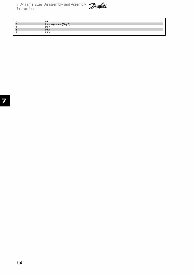
7/16/2019 1. D & E Frame.pdf
http://slidepdf.com/reader/full/1-d-e-framepdf 116/197
1 MK12 Retaining screw (Step 2)3 MK24 MK45 MK3
7 D-Frame Sizes Disassembly and AssemblyInstructions
116
7
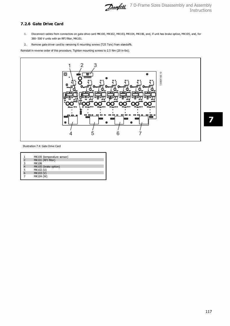
7/16/2019 1. D & E Frame.pdf
http://slidepdf.com/reader/full/1-d-e-framepdf 117/197
7.2.6 Gate Drive Card
1. Disconnect cables from connectors on gate drive card MK100, MK102, MK103, MK104, MK106, and, if unit has brake option, MK105, and, for
380- 500 V units with an RFI filter, MK101.
2. Remove gate driver card by removing 6 mounting screws (T25 Torx) from standoffs.
Reinstall in reverse order of this procedure. Tighten mounting screws to 2.5 Nm (20 in-lbs).
1 3 0 B X 1 6 0 . 1
0
2 3
4 5 6 7
1
Illustration 7.4: Gate Drive Card
1 MK100 (temperature sensor)2 MK101 (RFI filter)3 MK1064 MK105 (brake option)5 MK102 (U)6 MK103 (V)7 MK104 (W)
7 D-Frame Sizes Disassembly and AssemblyInstructions
117
7

7/16/2019 1. D & E Frame.pdf
http://slidepdf.com/reader/full/1-d-e-framepdf 118/197
7.2.7 Capacitor Bank(s)
Some D2/D4 size units have 2 capacitor bank assemblies mounted one above the other. Separate disassembly instructions are given
for upper and lower capacitor banks. For units with one capacitor bank assembly only, disassemble in accordance with instructions for
Single capacitor bank D1/D3 units .
Upper capacitor bank D2/D4 units
1. Remove control assembly support bracket in accordance with instructions.
2. Capacitor bank connection to DC bus bars can be seen recessed in the gap between upper and lower cap banks. Remove left most 2 nuts (10mm)
from DC bus bars. A minimum 100mm (4 in) extension is required.
3. Remove 4 retaining nuts (10 mm) from cap bank cover plate and remove cover plate.
4. Note that weight of cap bank is approximately 9 kg (20 lbs). Remove cap bank by pulling free from mounting studs.
Reinstall in reverse order of this procedure. Tighten mounting screws to 4 Nm (35 in-lbs).
1 3 0 B X 7 3 . 1 0
2 3
4 5
1
6
Illustration 7.5: D2/D4 Upper and Lower Capacitor Bank Assemblies
380-480/500V: Blue wire leads. 525-690V: Black wire leads.
1 Upper cap bank assy retaining nuts (step 2) 4 Lower cover plate retaining nut (step 3)2 Upper cover plate 5 Gate drive card3 Upper cover plate retaining nut (step 3) 6 Lower cap bank assy retaining nuts (step 1)
Lower capacitor bank D2/D4 units
1. Capacitor bank connection to DC bus bars can be seen recessed in the gap between upper and lower cap banks. Remove right most 2 cap bank
retaining nuts (10mm) from DC bus bars. A minimum 100mm (4 in) extension is required.
2. Note that IGBT gate drive card can remain attached to cap bank cover plate. Disconnect MK100, MK102, MK103, MK104, and MK106 from gate
drive card. Also remove MK105, for units with brake, and MK101 for units with RFI filter.
7 D-Frame Sizes Disassembly and AssemblyInstructions
118
7

7/16/2019 1. D & E Frame.pdf
http://slidepdf.com/reader/full/1-d-e-framepdf 119/197
3. Remove 4 retaining nuts (10mm) from cap bank cover plate and remove plate.
4. Note that weight of cap bank is approximately 9 kg (20 lbs). Remove cap bank by pulling free from mounting studs.
Reinstall in reverse order of this procedure. Tighten mounting screws to 4 Nm (35 in-lbs).
Single capacitor bank D1/D3 units
1. Remove control assembly support bracket in accordance with instructions.
2. Remove 2 capacitor bank retaining nuts (10mm) from DC bus bars. A minimum 100mm (4 in) extension is required.
3. Note that IGBT gate drive card can remain attached to cap bank cover plate. Disconnect MK100, MK102, MK103, MK104, and MK106 from gate
drive card. Also remove MK105, for units with brake, and MK101 for units with RFI filter.
4. Remove 4 retaining nuts (10mm) from cap bank cover plate and remove plate.
5. Note that weight of cap bank is approximately 9 kg (20 lbs). Remove cap bank by pulling free from mounting studs.
Reinstall in reverse order of this procedure. Tighten mounting screws to 4 Nm (35 in-lbs).
1 3 0 B X
7 2 . 1 0
1
2 3
Illustration 7.6: D1/D3 Single Capacitor Bank Assembly
380-480/500V: Blue wire leads. 525-690V: Black wire leads.
1 Retaining nuts (step 2)2 Retaining nuts (step 4)
3 Gate drive card (step 3)
7 D-Frame Sizes Disassembly and AssemblyInstructions
119
7
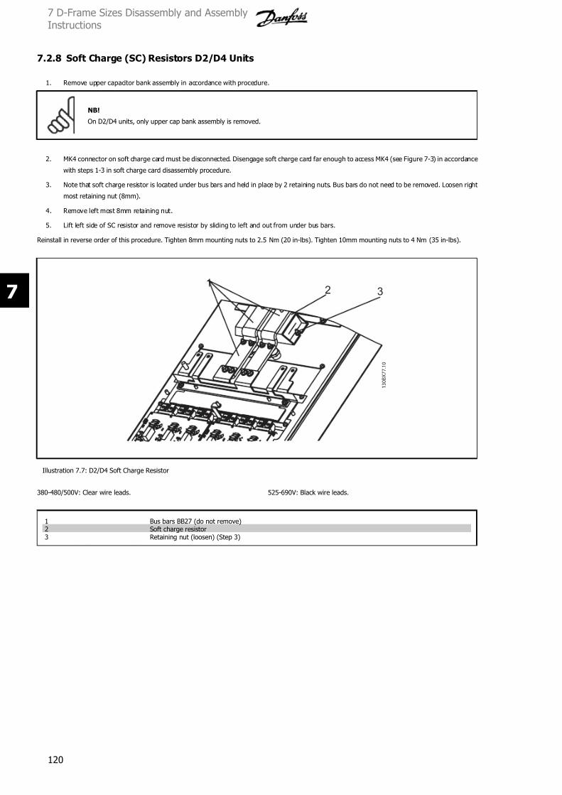
7/16/2019 1. D & E Frame.pdf
http://slidepdf.com/reader/full/1-d-e-framepdf 120/197
7.2.8 Soft Charge (SC) Resistors D2/D4 Units
1. Remove upper capacitor bank assembly in accordance with procedure.
NB!
On D2/D4 units, only upper cap bank assembly is removed.
2. MK4 connector on soft charge card must be disconnected. Disengage soft charge card far enough to access MK4 (see Figure 7-3) in accordance
with steps 1-3 in soft charge card disassembly procedure.
3. Note that soft charge resistor is located under bus bars and held in place by 2 retaining nuts. Bus bars do not need to be removed. Loosen right
most retaining nut (8mm).
4. Remove left most 8mm retaining nut.
5. Lift left side of SC resistor and remove resistor by sliding to left and out from under bus bars.
Reinstall in reverse order of this procedure. Tighten 8mm mounting nuts to 2.5 Nm (20 in-lbs). Tighten 10mm mounting nuts to 4 Nm (35 in-lbs).
1 3 0 B X 7 7 . 1 0
12 3
Illustration 7.7: D2/D4 Soft Charge Resistor
380-480/500V: Clear wire leads. 525-690V: Black wire leads.
1 Bus bars BB27 (do not remove)2 Soft charge resistor3 Retaining nut (loosen) (Step 3)
7 D-Frame Sizes Disassembly and AssemblyInstructions
120
7

7/16/2019 1. D & E Frame.pdf
http://slidepdf.com/reader/full/1-d-e-framepdf 121/197
7.2.9 Soft Charge (SC) Resistors D1/D3 Units
1. Remove capacitor bank per instruction.
2. Remove input terminal mounting plate per instructions.
3. Note the color coding for each of three wires attached to terminal 1 for each SCR/Diode module. Ensure that correct wire is attached to applicable
stud upon reassembling. Remove wiring from studs. Remove retaining screw (T25) from terminal 1 of each of 3 SCR/Diode modules and remove
bus bar.
CONTINUED ON NEXT PAGE
1 3 0 B X 8 7 . 1 0
1
2
3
Illustration 7.8: D1/D2 Soft Charge Resistor (1 of 3)
380-480/500V: Clear wire leads. 525-690V: Black wire leads.
1 Soft charge resistor2 Bus bar BB2 (Step 3)3 Retaining screw (Step 3)
7 D-Frame Sizes Disassembly and AssemblyInstructions
121
7
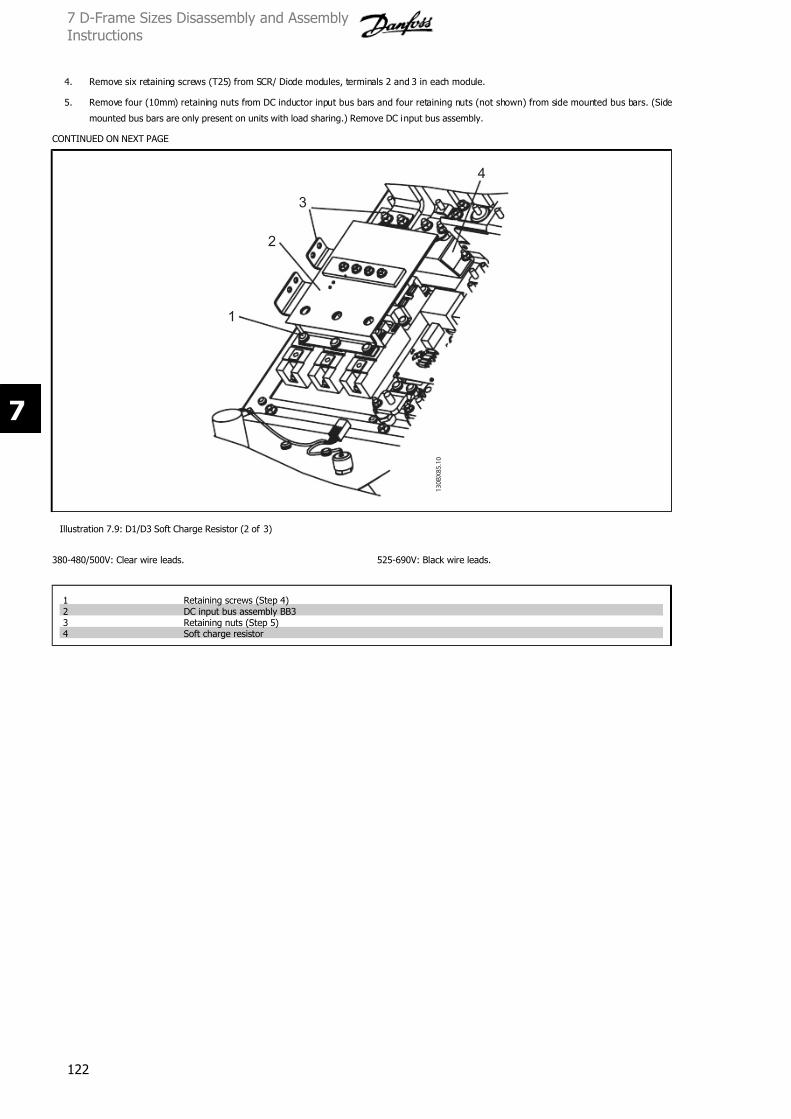
7/16/2019 1. D & E Frame.pdf
http://slidepdf.com/reader/full/1-d-e-framepdf 122/197
4. Remove six retaining screws (T25) from SCR/ Diode modules, terminals 2 and 3 in each module.
5. Remove four (10mm) retaining nuts from DC inductor input bus bars and four retaining nuts (not shown) from side mounted bus bars. (Side
mounted bus bars are only present on units with load sharing.) Remove DC input bus assembly.
CONTINUED ON NEXT PAGE
1 3 0 B X 8 5 . 1 0
1
2
3
4
Illustration 7.9: D1/D3 Soft Charge Resistor (2 of 3)
380-480/500V: Clear wire leads. 525-690V: Black wire leads.
1 Retaining screws (Step 4)2 DC input bus assembly BB33 Retaining nuts (Step 5)4 Soft charge resistor
7 D-Frame Sizes Disassembly and AssemblyInstructions
122
7

7/16/2019 1. D & E Frame.pdf
http://slidepdf.com/reader/full/1-d-e-framepdf 123/197
6. Remove soft charge resistor by removing two mounting screws.
Reassembly
1. Clean heatsink surface with mild solvent or alcohol solution.
2. Reassemble remaining parts in reverse order of their removal. Tighten T25 and 8mm mounting screws to 2.5 Nm (20 in-lbs) and T30 and 10
mm to 4 Nm (35 in-lbs).
1 3 0 B X 8 3 . 1 0
1
2
Illustration 7.10: D1/D3 Soft Charge Resistor (3 of 3)
380-480/500V: Clear wire leads. 525-690V: Black wire leads.
1 Soft charge resistor2 Mounting screws (Step 6)
7 D-Frame Sizes Disassembly and AssemblyInstructions
123
7

7/16/2019 1. D & E Frame.pdf
http://slidepdf.com/reader/full/1-d-e-framepdf 124/197
7.2.10 Input Terminal Mounting Plate Assembly
1. Disconnect input power wiring from L1, L2, L3, and ground connection.
2. Remove upper most bus bar retaining nuts (13mm) from AC power input bus bars L1, L2, and L3.
3. Disconnect fan autotransformer cable at in-line connector.
4. Remove 4 or 5 (10mm) retaining nuts (varies with size) from mounting plate.
Input terminal mounting plate weighs approximately 7 - 27 kg lbs (15 - 60), depending on mounted options.
5. Remove entire assembly from mounting studs.
Reinstall in reverse order of this procedure. Tighten 10mm mounting nuts to 4 Nm (35 in-lbs). and 13mm nuts to 9.5 Nm (85 in-lb).
1 3 0 B X 8 1 . 1 0
1
2
34
Illustration 7.11: Input Terminal Mounting Plate Assembly (no options shown)
380-480/500V: White label on fan transformer. 525-690V: Orange label on fan transformer.
1 Input power connector (Step 1)2 Bus bar retaining nuts (shown removed) (Step 2)3 Transformer connector (Step 3)4 Retaining nuts (Step 4)
7 D-Frame Sizes Disassembly and AssemblyInstructions
124
7
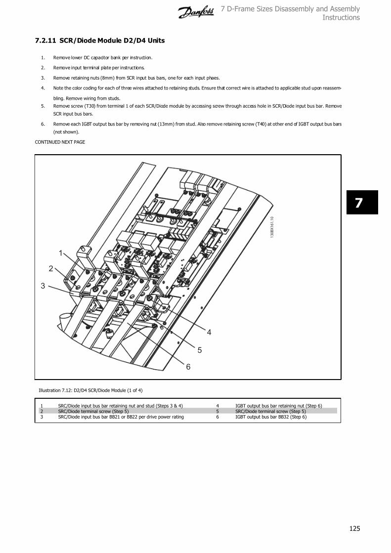
7/16/2019 1. D & E Frame.pdf
http://slidepdf.com/reader/full/1-d-e-framepdf 125/197
7.2.11 SCR/Diode Module D2/D4 Units
1. Remove lower DC capacitor bank per instruction.
2. Remove input terminal plate per instructions.
3. Remove retaining nuts (8mm) from SCR input bus bars, one for each input phaes.
4. Note the color coding for each of three wires attached to retaining studs. Ensure that correct wire is attached to applicable stud upon reassem-
bling. Remove wiring from studs.
5. Remove screw (T30) from terminal 1 of each SCR/Diode module by accessing screw through access hole in SCR/Diode input bus bar. Remove
SCR input bus bars.
6. Remove each IGBT output bus bar by removing nut (13mm) from stud. Also remove retaining screw (T40) at other end of IGBT output bus bars
(not shown).
CONTINUED NEXT PAGE
1 3 0 B X 1 6 1 . 1 0
1
2
3
4
5
6
Illustration 7.12: D2/D4 SCR/Diode Module (1 of 4)
1 SRC/Diode input bus bar retaining nut and stud (Steps 3 & 4) 4 IGBT output bus bar retaining nut (Step 6)2 SRC/Diode terminal screw (Step 5) 5 SRC/Diode terminal screw (Step 5)3 SRC/Diode input bus bar BB21 or BB22 per drive power rating 6 IGBT output bus bar BB32 (Step 6)
7 D-Frame Sizes Disassembly and AssemblyInstructions
125
7
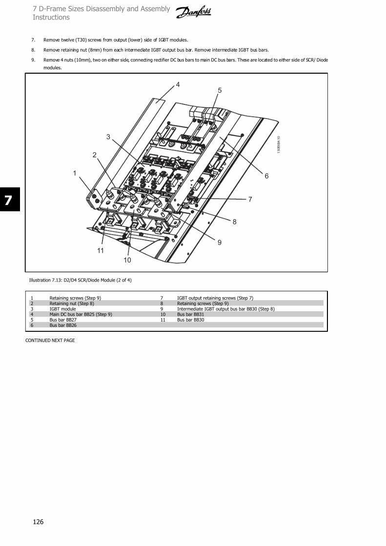
7/16/2019 1. D & E Frame.pdf
http://slidepdf.com/reader/full/1-d-e-framepdf 126/197
7. Remove twelve (T30) screws from output (lower) side of IGBT modules.
8. Remove retaining nut (8mm) from each intermediate IGBT output bus bar. Remove intermediate IGBT bus bars.
9. Remove 4 nuts (10mm), two on either side, connecting rectifier DC bus bars to main DC bus bars. These are located to either side of SCR/ Diode
modules.
1 3 0 B X 8 4 . 1 0
1
2
3
45
6
7
8
9
10
11
Illustration 7.13: D2/D4 SCR/Diode Module (2 of 4)
1 Retaining screws (Step 9) 7 IGBT output retaining screws (Step 7)2 Retaining nut (Step 8) 8 Retaining screws (Step 9)3 IGBT module 9 Intermediate IGBT output bus bar BB30 (Step 8)4 Main DC bus bar BB25 (Step 9) 10 Bus bar BB315 Bus bar BB27 11 Bus bar BB306 Bus bar BB26
CONTINUED NEXT PAGE
7 D-Frame Sizes Disassembly and AssemblyInstructions
126
7

7/16/2019 1. D & E Frame.pdf
http://slidepdf.com/reader/full/1-d-e-framepdf 127/197
7 D-Frame Sizes Disassembly and AssemblyInstructions
127
7
7/16/2019 1. D & E Frame.pdf
http://slidepdf.com/reader/full/1-d-e-framepdf 128/197
1 Bus bar BB272 Bus bar BB283 Retaining screws (Step 10)4 Rectifier DC bus bars BB23 or BB24 per drive power rating (Step 10)
7 D-Frame Sizes Disassembly and AssemblyInstructions
128
7
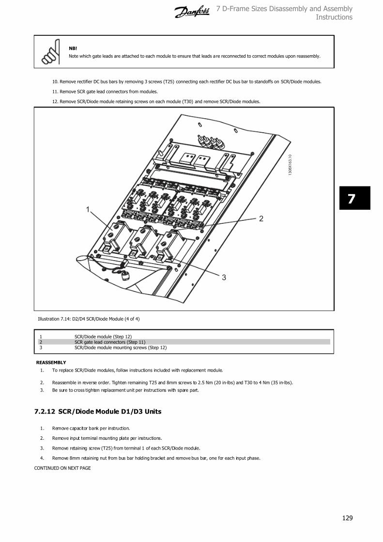
7/16/2019 1. D & E Frame.pdf
http://slidepdf.com/reader/full/1-d-e-framepdf 129/197
NB!
Note which gate leads are attached to each module to ensure that leads are reconnected to correct modules upon reassembly.
10. Remove rectifier DC bus bars by removing 3 screws (T25) connecting each rectifier DC bus bar to standoffs on SCR/Diode modules.
11. Remove SCR gate lead connectors from modules.
12. Remove SCR/Diode module retaining screws on each module (T30) and remove SCR/Diode modules.
1 3 0 B X 1 6 3 . 1 0
1
2
3
Illustration 7.14: D2/D4 SCR/Diode Module (4 of 4)
1 SCR/Diode module (Step 12)2 SCR gate lead connectors (Step 11)3 SCR/Diode module mounting screws (Step 12)
REASSEMBLY
1. To replace SCR/Diode modules, follow instructions included with replacement module.
2. Reassemble in reverse order. Tighten remaining T25 and 8mm screws to 2.5 Nm (20 in-lbs) and T30 to 4 Nm (35 in-lbs).
3. Be sure to cross tighten replacement unit per instructions with spare part.
7.2.12 SCR/Diode Module D1/D3 Units
1. Remove capacitor bank per instruction.
2. Remove input terminal mounting plate per instructions.
3. Remove retaining screw (T25) from terminal 1 of each SCR/Diode module.
4. Remove 8mm retaining nut from bus bar holding bracket and remove bus bar, one for each input phase.
CONTINUED ON NEXT PAGE
7 D-Frame Sizes Disassembly and AssemblyInstructions
129
7

7/16/2019 1. D & E Frame.pdf
http://slidepdf.com/reader/full/1-d-e-framepdf 130/197
1 3 0 B X 1 6 5 . 1 0
1
2
3
4
5
Illustration 7.15: D1/D3 SCR/Diode Module (1 of 3)
1 Bus bar BB2 (Step 4)2 Retaining screw access (Step 3)3 Retaining nut (Step 4)4 Bus bar BB15 SCR/Diode module
7 D-Frame Sizes Disassembly and AssemblyInstructions
130
7

7/16/2019 1. D & E Frame.pdf
http://slidepdf.com/reader/full/1-d-e-framepdf 131/197
5. Remove six retaining screws (T25) from SCR/ Diode modules, terminals 2 and 3 in each module.
6. Remove four (10mm) retaining nuts from DC inductor input bus bars and four retaining nuts (not shown) from side mounted bus bars. (Side
mounted bus bars are only present on units with load sharing.) Remove DC input bus assembly.
CONTINUED ON NEXT PAGE
1 3 0 B X 9 3 . 1 0
1
2
3
4
5
Illustration 7.16: D1/D3 SCR/Diode Module (2 of 3)
1 Bus bar BB42 Retaining nuts (Step 6)3 DC input bus assembly BB3 (Step 6)4 Retaining screws (Step 5)5 SCR/Diode module
7 D-Frame Sizes Disassembly and AssemblyInstructions
131
7

7/16/2019 1. D & E Frame.pdf
http://slidepdf.com/reader/full/1-d-e-framepdf 132/197
7. Note which gate leads attach to which module for reasembly. Remove SCR/Diode gate lead connectors from modules (not shown).
8. If unit is equipped with brake option, remove two bus bars attaching brake IGBT module to IGBT bus assy. Remove SCR/Diode mounting
screws.
REASSEMBLY
1. To replace SCR/Diode modules, follow instructions included with replacement module.
2. Reinstall module and mounting screws. Tighten remaining T25 and 8mm screws to 2.5 Nm (20 in-lbs) and T30 and 10 mm to 4 Nm (35 in-lbs).
3. Reassemble remaining parts in reverse order of their removal.
1 3 0 B X 9 2 . 1 0
1
2
Illustration 7.17: D1/D3 SCR/Diode Module (3 of 3)
1 SCR/Diode module2 Mounting screws (Step 8)
7 D-Frame Sizes Disassembly and AssemblyInstructions
132
7
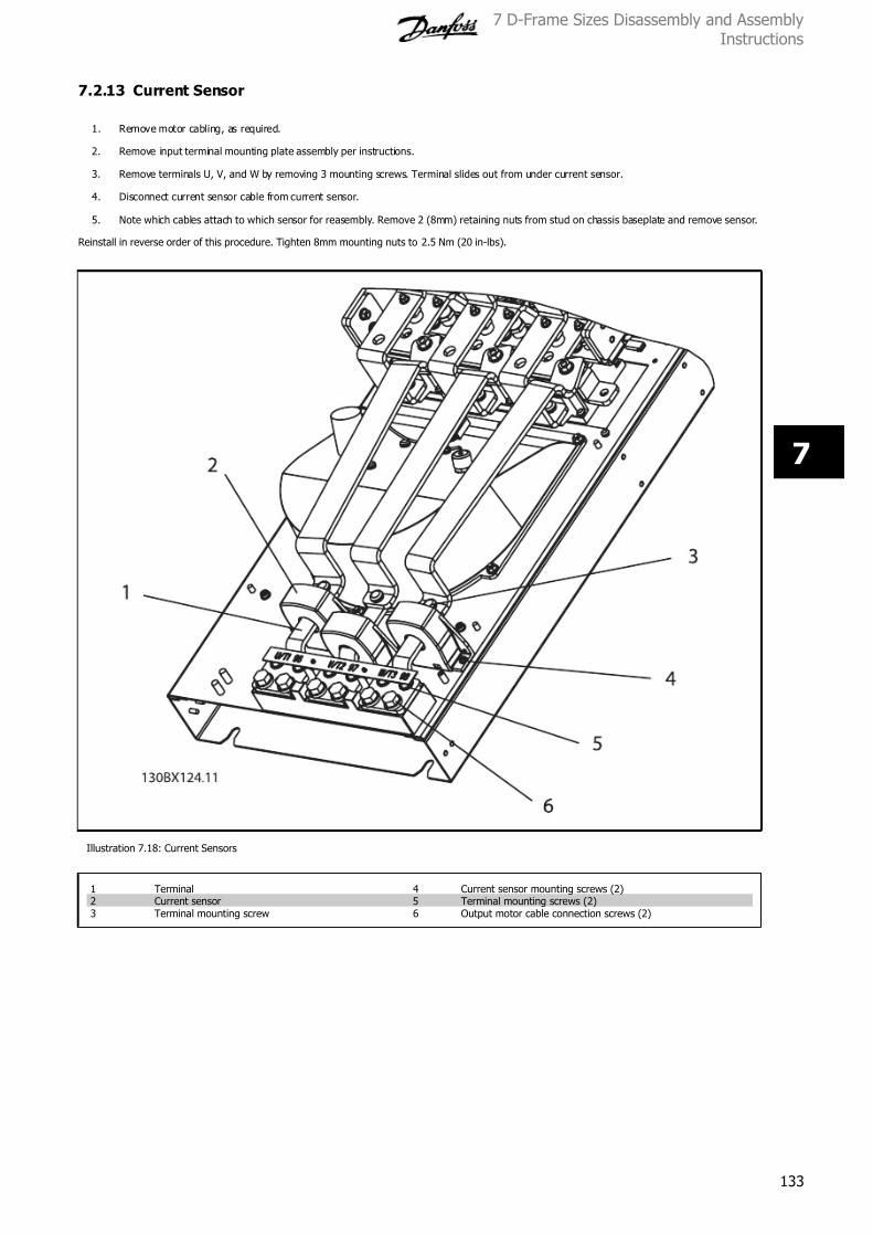
7/16/2019 1. D & E Frame.pdf
http://slidepdf.com/reader/full/1-d-e-framepdf 133/197
7.2.13 Current Sensor
1. Remove motor cabling, as required.
2. Remove input terminal mounting plate assembly per instructions.
3. Remove terminals U, V, and W by removing 3 mounting screws. Terminal slides out from under current sensor.
4. Disconnect current sensor cable from current sensor.
5. Note which cables attach to which sensor for reasembly. Remove 2 (8mm) retaining nuts from stud on chassis baseplate and remove sensor.
Reinstall in reverse order of this procedure. Tighten 8mm mounting nuts to 2.5 Nm (20 in-lbs).
Illustration 7.18: Current Sensors
1 Terminal 4 Current sensor mounting screws (2)2 Current sensor 5 Terminal mounting screws (2)3 Terminal mounting screw 6 Output motor cable connection screws (2)
7 D-Frame Sizes Disassembly and AssemblyInstructions
133
7
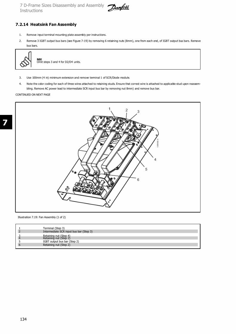
7/16/2019 1. D & E Frame.pdf
http://slidepdf.com/reader/full/1-d-e-framepdf 134/197
7.2.14 Heatsink Fan Assembly
1. Remove input terminal mounting plate assembly per instructions.
2. Remove 3 IGBT output bus bars (see Figure 7-19) by removing 6 retaining nuts (8mm), one from each end, of IGBT output bus bars. Remove
bus bars.
NB!Omit steps 3 and 4 for D2/D4 units.
3. Use 100mm (4 in) minimum extension and remove terminal 1 of SCR/Diode module.
4. Note the color coding for each of three wires attached to retaining studs. Ensure that correct wire is attached to applicable stud upon reassem-
bling. Remove AC power lead to intermediate SCR input bus bar by removing nut 8mm) and remove bus bar.
CONTINUED ON NEXT PAGE
1 3 0 B X 8 8 . 1 0
1 213
4
6
5
Illustration 7.19: Fan Assembly (1 of 2)
1 Terminal (Step 3)2 Intermediate SCR input bus bar (Step 3)
3 Retaining nut (Step 4)4 Retaining nut (Step 2)5 IGBT output bus bar (Step 2)6 Retaining nut (Step 2)
7 D-Frame Sizes Disassembly and AssemblyInstructions
134
7
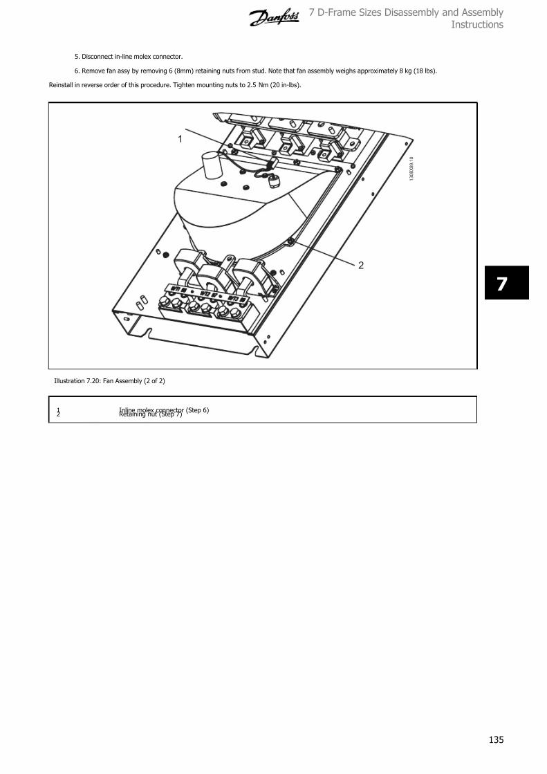
7/16/2019 1. D & E Frame.pdf
http://slidepdf.com/reader/full/1-d-e-framepdf 135/197
5. Disconnect in-line molex connector.
6. Remove fan assy by removing 6 (8mm) retaining nuts f rom stud. Note that fan assembly weighs approximately 8 kg (18 lbs).
Reinstall in reverse order of this procedure. Tighten mounting nuts to 2.5 Nm (20 in-lbs).
1 3 0 B X 8 9 . 1 0
1
2
Illustration 7.20: Fan Assembly (2 of 2)
1 Inline molex connector (Step 6)2 Retaining nut (Step 7)
7 D-Frame Sizes Disassembly and AssemblyInstructions
135
7
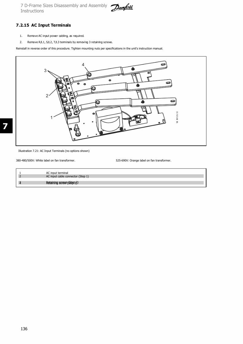
7/16/2019 1. D & E Frame.pdf
http://slidepdf.com/reader/full/1-d-e-framepdf 136/197
7.2.15 AC Input Terminals
1. Remove AC input power cabling, as required.
2. Remove R/L1, S/L2, T/L3 terminals by removing 3 retaining screws.
Reinstall in reverse order of this procedure. Tighten mounting nuts per specifications in the unit's instruction manual.
1 3 0
B X 1 2 5 . 1 0
1
2
3
4
Illustration 7.21: AC Input Terminals (no options shown)
380-480/500V: White label on fan transformer. 525-690V: Orange label on fan transformer.
1 AC input terminal2 AC input cable connector (Step 1)
3 Retaining screws (Step 2)4 Retaining screw (Step 2)
7 D-Frame Sizes Disassembly and AssemblyInstructions
136
7

7/16/2019 1. D & E Frame.pdf
http://slidepdf.com/reader/full/1-d-e-framepdf 137/197
7.2.16 IGBT Modules D2/D4 Units
1. Remove capacitor banks per instructions.
2. Note IGBT gate signal cables connected between gate drive card connectors MK100 (temperature sensor), MK102 (U), MK103 (V), and MK104
(W) and IGBTs. These will need to be reconnected in same locations during reassembly. Units with brake option will have brake cabling from
MK105 in addition. Disconnect cables at connectors on IGBT modules.
3. Remove retaining nuts (8mm) from SCR input bus bars.
4. Note the color coding for each of three wires attached to retaining studs. Ensure that correct wire is attached to applicable stud upon reassem-
bling. Remove wiring from studs.
5. Remove screw (T25) from terminal 1 of each SCR/Diode module by accessing screw through access hole in SCR/Diode input bus bar. Remove
SCR input bus bars.
6. Remove each IGBT output bus bar by removing nut (10mm) from stud. Also remove retaining screw (T30) at other end of IGBT output bus bars
(not shown).
CONTINUED ON NEXT PAGE
1 3 0 B X 9 1 . 1 0
1
2
3
4
5
61
1
7
8
Illustration 7.22: D2/D4 IGBT Modules (1 of 3)
1 SCR/Diode input bus bar BB21 or BB22 per drive power rating 5 Snubber capacitor2 SCR/Diode terminal screw (Step 5) 6 IGBT output bus bar retaining nut (Step 6)3 SCR/Diode input bus bar retaining nut and stud (Steps 3 & 4) 7 SCR/Diode terminal screw (Step 5)4 IGBT gate signal input terminal (Step 2) 8 IGBT output bus bar BB32 (Step 6)
7 D-Frame Sizes Disassembly and AssemblyInstructions
137
7
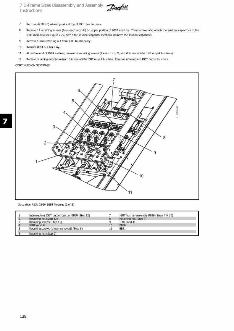
7/16/2019 1. D & E Frame.pdf
http://slidepdf.com/reader/full/1-d-e-framepdf 138/197
7. Remove 4 (10mm) retaining nuts at top of IGBT bus bar assy.
8. Remove 12 retaining screws (6 on each module) on upper portion of IGBT modules. These screws also attach the snubber capacitors to the
IGBT modules (see Figure 7-22, item 5 for snubber capacitor location). Remove the snubber capacitors.
9. Remove 10mm retaining nut from IGBT bus bar assy.
10. Remove IGBT bus bar assy.
11. At bottom end of IGBT module, remove 12 retaining screws (4 each for U, V, and W intermediate IGBT output bus bars).
12. Remove retaining nut (8mm) from 3 intermediate IGBT output bus bars. Remove intermediate IGBT output bus bars.
CONTINUED ON NEXT PAGE
1
3 0 B X 9 8 . 1 0
2
3
4
5
6
7
8
9
10
11
Illustration 7.23: D2/D4 IGBT Modules (2 of 3)
1 Intermediate IGBT output bus bar BB30 (Step 12) 7 IGBT bus bar assembly BB29 (Steps 7 & 10)2 Retaining nut (Step 12) 8 Retaining nut (Step 7)3 Retaining screws (Step 11) 9 IGBT module4 IGBT module 10 BB305 Retaining screws (shown removed) (Step 8) 11 BB31
6 Retaining nut (Step 9)
7 D-Frame Sizes Disassembly and AssemblyInstructions
138
7
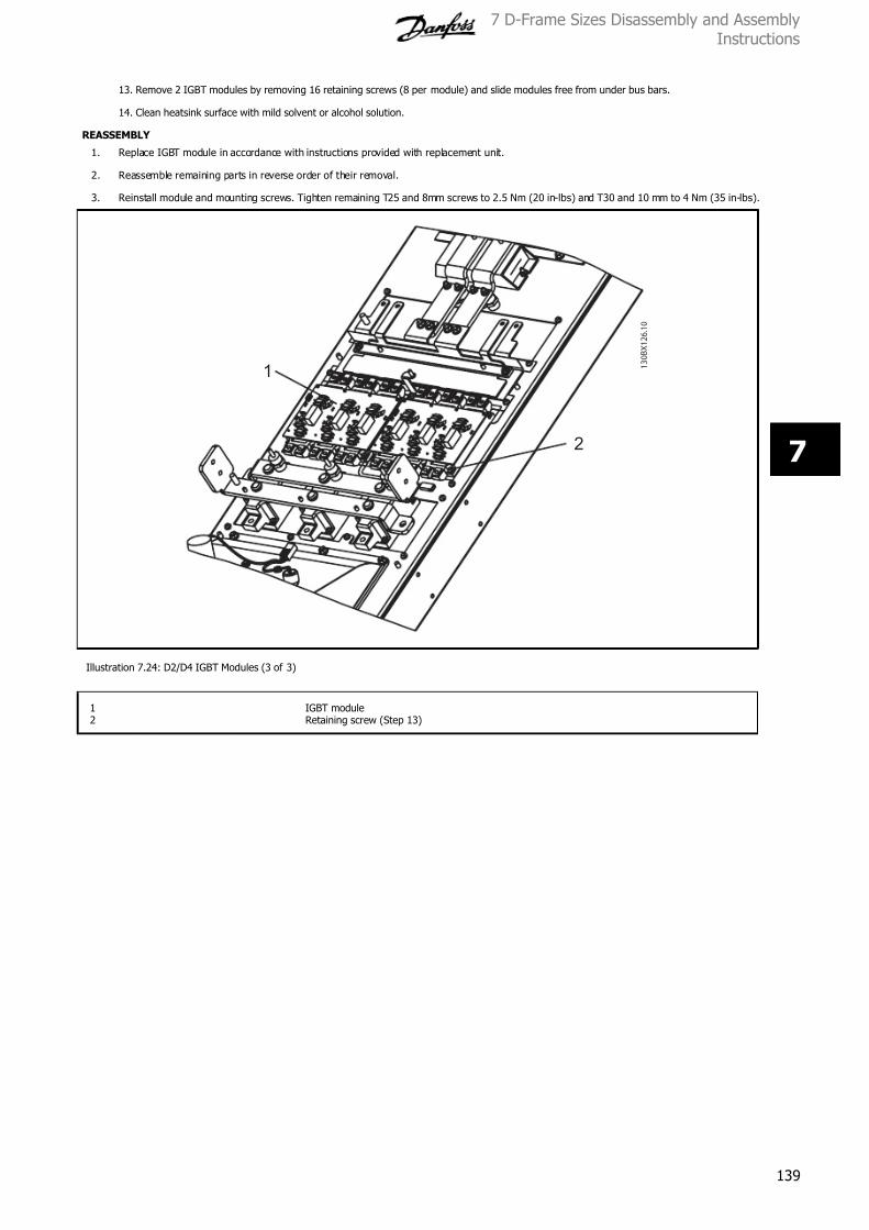
7/16/2019 1. D & E Frame.pdf
http://slidepdf.com/reader/full/1-d-e-framepdf 139/197
13. Remove 2 IGBT modules by removing 16 retaining screws (8 per module) and slide modules free from under bus bars.
14. Clean heatsink surface with mild solvent or alcohol solution.
REASSEMBLY
1. Replace IGBT module in accordance with instructions provided with replacement unit.
2. Reassemble remaining parts in reverse order of their removal.
3. Reinstall module and mounting screws. Tighten remaining T25 and 8mm screws to 2.5 Nm (20 in-lbs) and T30 and 10 mm to 4 Nm (35 in-lbs).
1 3 0 B X 1 2 6 . 1 0
1
2
Illustration 7.24: D2/D4 IGBT Modules (3 of 3)
1 IGBT module2 Retaining screw (Step 13)
7 D-Frame Sizes Disassembly and AssemblyInstructions
139
7

7/16/2019 1. D & E Frame.pdf
http://slidepdf.com/reader/full/1-d-e-framepdf 140/197
7.2.17 IGBT modules D1/D3 units
1. Remove control card cassette per instructions.
2. Remove input terminal mounting plate per instructions.
3. Note IGBT gate signal cables connected between gate drive card connectors MK100 (temperature sensor), MK102 (U), MK103 (V), and MK104
(W) and IGBT module connectors. These will need to be reconnected in same locations during reassembly. Units with brake option will have
brake cabling from MK105 in addition. Remove capacitor bank per instructions.
4. Disconnect gate drive cables at connectors on IGBT modules.
5. Disconnect cable connected to connector MK100 on high frequency card.
6. Remove high frequency card by removing 2 retaining screws and 1 retaining nut.
6a For units with brake option, DC input bus assembly must be removed to access and remove bus bars between IGBT bus bar assembly
and brake IGBT. Remove DC input bus bar assembly per steps 3 - 5 of SCR/Diode Module Removal (D1 units).
6b For units with brake option, remove bus bars between IGBT bus bar assembly and brake IGBT by removing two T25 retaining screws
on brake IGBT (not shown) and two 8mm retaining nuts on IGBT bus bar assembly (not shown).
7. Remove 3 IGBT output bus bars by removing nut (10mm) from stud. Also remove retaining screw (T30) at other end of IGBT output bus bars
(not shown).
CONTINUED ON NEXT PAGE
1 3 0 B X 9 0 . 1 0
1
2
3 4 5
6
7
8
9
10
Illustration 7.25: D1/D3 IGBT Module (1 of 2)
1 IGBT output bus bar BB9 (Step 7) 6 Retaining nut (Step 6)2 DC input bus bar assembly BB3 (Step 6A) 7 Do not remove (Step 6)3 Retaining screw (Step 6) 8 Gate drive cable connectors (Steps 3 & 4)4 High frequency card 9 IGBT module5 Connector MK100 (Step 5) 10 IGBT output bus bar retaining nut (Step 7)
7 D-Frame Sizes Disassembly and AssemblyInstructions
140
7
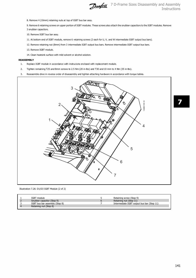
7/16/2019 1. D & E Frame.pdf
http://slidepdf.com/reader/full/1-d-e-framepdf 141/197
8. Remove 4 (10mm) retaining nuts at top of IGBT bus bar assy.
9. Remove 6 retaining screws on upper portion of IGBT modules. These screws also attach the snubber capacitors to the IGBT modules. Remove
3 snubber capacitors.
10. Remove IGBT bus bar assy.
11. At bottom end of IGBT module, remove 6 retaining screws (2 each for U, V, and W intermediate IGBT output bus bars).
12. Remove retaining nut (8mm) from 3 intermediate IGBT output bus bars. Remove intermediate IGBT output bus bars.
13. Remove IGBT module.
14. Clean heatsink surface with mild solvent or alcohol solution.
REASSEMBLY
1. Replace IGBT module in accordance with instrucions enclosed with replacement module.
2. Tighten remaining T25 and 8mm screws to 2.5 Nm (20 in-lbs) and T30 and 10 mm to 4 Nm (35 in-lbs).
3. Reassemble drive in reverse order of disassembly and tighten attaching hardware in accordance with torque tables.
1 3 0 B X 1 5 9 . 1 0
1
2
3
4
5
6
7
Illustration 7.26: D1/D3 IGBT Module (2 of 2)
1 IGBT module 5 Retaining screw (Step 9)2 Snubber capacitor (Step 9) 6 Retaining nut (Step 11)3 IGBT bus bar assembly (Step 8) 7 Intermediate IGBT output bus bar (Step 11)4 Retaining nut (Step 8)
7 D-Frame Sizes Disassembly and AssemblyInstructions
141
7

7/16/2019 1. D & E Frame.pdf
http://slidepdf.com/reader/full/1-d-e-framepdf 142/197
8 E-Frame Sizes Disassembly and AssemblyInstructions
142
8

7/16/2019 1. D & E Frame.pdf
http://slidepdf.com/reader/full/1-d-e-framepdf 143/197
8 E-Frame Sizes Disassembly and Assembly Instructions
8.1 Electrostatic Discharge (ESD)
Drives contain dangerous voltages when connected to line voltage. No disassembly should be attempted with power applied. Remove
power to drive and wait at least 40 minutes to let drive capacitors fully discharge. Only a competent technician should carry out service.
ELECTROSTATIC DISCHARGE (ESD)
Many electronic components within the adjustable frequency drive are sensitive to static electricity. Voltages so low that they cannot be felt, seen or
heard can reduce the life, affect performance, or completely destroy sensitive electronic components.
Use proper electrostatic discharge (ESD) procedures when servicing drive to prevent damage to sensitive components.
NB!
Frame size is used throughout this manual where ever procedures or components differ between drives based upon the unit's physical
size. Refer to tables in the Introduction Section to determine E-frame size definitions.
8 E-Frame Sizes Disassembly and AssemblyInstructions
143
8

7/16/2019 1. D & E Frame.pdf
http://slidepdf.com/reader/full/1-d-e-framepdf 144/197
8.2 Instructions
8.2.1 Control Card and Control Card Mounting Plate
1. Open front panel door or remove front cover, depending on unit type.
2. (See Figure 8-1) Unplug LCP keypad ribbon cable (not shown) from control card or remove LCP, depending on unit type. LCP removes by hand.
3. Remove LCP cradle. LCP cradle removes by hand.
4. Remove any customer control wiring from control card terminal blocks.
5. Remove 4 screws (T20 Torx) securing control card mounting plate to control assembly support bracket.
6. Unplug ribbon cable from back of control card.
Reinstall in reverse order of this procedure. The red conductor on the ribbon cable between the control card and the power card should be on the bottom
of the connector. Tighten control card mounting plate screws to 1 Nm (8 in-lb).
8 E-Frame Sizes Disassembly and AssemblyInstructions
144
8
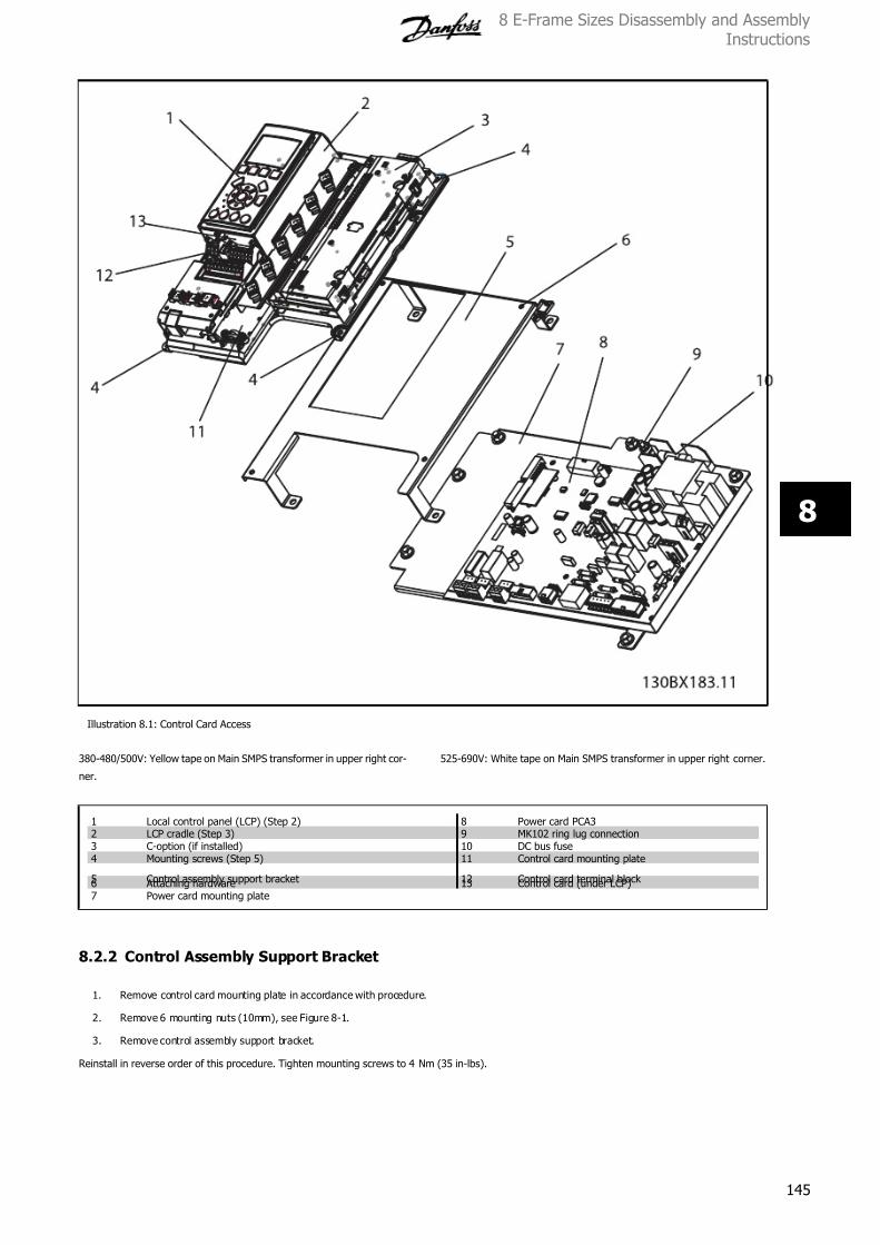
7/16/2019 1. D & E Frame.pdf
http://slidepdf.com/reader/full/1-d-e-framepdf 145/197
Illustration 8.1: Control Card Access
380-480/500V: Yellow tape on Main SMPS transformer in upper right cor-
ner.
525-690V: White tape on Main SMPS transformer in upper right corner.
1 Local control panel (LCP) (Step 2) 8 Power card PCA32 LCP cradle (Step 3) 9 MK102 ring lug connection3 C-option (if installed) 10 DC bus fuse4 Mounting screws (Step 5) 11 Control card mounting plate
5 Control assembly support bracket 12 Control card terminal block 6 Attaching hardware 13 Control card (under LCP)7 Power card mounting plate
8.2.2 Control Assembly Support Bracket
1. Remove control card mounting plate in accordance with procedure.
2. Remove 6 mounting nuts (10mm), see Figure 8-1.
3. Remove control assembly support bracket.
Reinstall in reverse order of this procedure. Tighten mounting screws to 4 Nm (35 in-lbs).
8 E-Frame Sizes Disassembly and AssemblyInstructions
145
8

7/16/2019 1. D & E Frame.pdf
http://slidepdf.com/reader/full/1-d-e-framepdf 146/197
8.2.3 Power Card
1. Remove control assembly support bracket in accordance with procedure.
2. Unplug power card connectors MK100, MK102, MK105, MK106, and MK107.
3. If customer connections are present, unplug connectors FK102, FK103, and MK112.
4. Remove 7 mounting screws (T25 Torx) from power card.
5. Remove power card from plastic standoff at top right of power card.
6. Remove current scaling card from power card by pushing in retaining clips on standoffs. KEEP THIS SCALING CARD TO REINSTALL ON ANY
REPLACEMENT POWER CARD. Scaling card controls signals operating with this specific VLT drive. Scaling card is not part of replacement power
card.
Reinstall in reverse order of this procedure. When installing the power card, ensure that the insulator sheet is installed behind the power card. Tighten
mounting screws to 2.5 Nm (20 in-lbs).
1
2
34
5
6
7
8
9
10
11
12
13
14
15
16
130BX172.10
Illustration 8.2: Power Card, and Mounting Plate
380-480/500V: Yellow tape on Main SMPS transformer in upper right cor-
ner.
525-690V: White tape on Main SMPS transformer in upper right corner.
1 Power card PCA3 9 MK1062 Mounting plate 10 MK1003 MK110 11 MK1094 MK102 12 FK1025 MK104 13 FK1016 MK105 14 FK1007 MK107 15 Current scaling card PCA48 FK103 16 Current scaling card standoff
8 E-Frame Sizes Disassembly and AssemblyInstructions
146
8

7/16/2019 1. D & E Frame.pdf
http://slidepdf.com/reader/full/1-d-e-framepdf 147/197
8.2.4 Soft Charge Card
1. Disconnect MK1, MK2, MK3, and MK4.
2. Remove 4 mounting screws (T25) from standoffs.
3. Remove soft charge card. Note insulation sheet below soft charge card. Remove and keep insulation with card for reinstallation.
Reinstall by mounting insulation onto standoffs. Mount soft charge card and tighten mounting screws to 2.5 Nm (20 in-lbs).
1 3 0 B X
1 5 5 . 1 0
3
4
2
5
1
Illustration 8.3: Soft Charge Card
380-480/500V: Blue MOV and 8 PTCs. 525-690V: Red MOV and 6 PTCs.
1 MK3 4 MK42 Mounting screw (Step 2) 5 MK23 MK1
8 E-Frame Sizes Disassembly and AssemblyInstructions
147
8

7/16/2019 1. D & E Frame.pdf
http://slidepdf.com/reader/full/1-d-e-framepdf 148/197
8.2.5 Gate Drive Card
1. Disconnect cables from connectors on gate drive card MK100, MK102, MK103, MK104, MK106, and, if unit has brake option, MK105, and, for
380-500 V units with an RFI filter, MK101.
2. Remove gate driver card by removing 6 mounting screws (T25 Torx) from standoffs.
Reinstall in reverse order of this procedure. Tighten mounting screws to 2.5 Nm (20 in-lbs).
1 3 0 B X 1 6 0 . 1
0
2 3
4 5 6 7
1
Illustration 8.4: Gate Drive Card.
1 MK100 5 MK102 (U)2 MK101 (RFI filter) 6 MK103 (V)3 MK106 7 MK104 (W)4 MK105 (brake option)
8 E-Frame Sizes Disassembly and AssemblyInstructions
148
8
7/16/2019 1. D & E Frame.pdf
http://slidepdf.com/reader/full/1-d-e-framepdf 149/197
8.2.6 Capacitor Banks
Upper Capacitor Banks
1. Remove control assembly support bracket and gate drive card in accordance with instructions.
2. Capacitor bank connection to DC bus bars can be seen recessed in gap between upper and lower capacitor banks. Minimum 6 inch (150 mm)
extension required. Remove 6 electrical connection nuts (8 mm) for upper capacitor bank from DC bus bars.
3. Remove 4 retaining nuts (10 mm) from capacitor bank and remove air dam.
4. Note that the weight of capacitor bank is approximately 20 pounds (9 kg). Remove capacitor bank by pulling free from mounting studs.
Reinstall in reverse order of this procedure. Tighten electrical connection nuts (8 mm) to 2.5 Nm (20 in-lbs) and mechanical connection nuts (10 mm) to
4 Nm (35 in-lbs).
Lower Capacitor Banks
1. Remove soft charge card in accordance with procedures.
2. Capacitor bank connection to DC bus bars can be seen recessed in gap between upper and lower capacitor banks. Minimum 150 mm (6 in)
extension is required. Remove 6 electrical connection nuts (8 mm) for lower capacitor bank from DC bus bars.
3. Remove 4 retaining nuts (10 mm) from capacitor bank.
4. Note that the weight of the capacitor bank is approximately 9 kg (20 lbs). Remove capacitor bank by pulling free from mounting studs.
Reinstall in reverse order of this procedure. Note: DO NOT over torque. Tighten electrical connection nuts (8 mm) to 2.5 Nm (20 in-lbs) and mechanical
connection nuts (10 mm) to 4 Nm (35 in-lbs).
8 E-Frame Sizes Disassembly and AssemblyInstructions
149
8

7/16/2019 1. D & E Frame.pdf
http://slidepdf.com/reader/full/1-d-e-framepdf 150/197
Illustration 8.5: Upper and Lower Capacitor Bank Assemblies
1* Upper capacitor bank assy 5* Lower capacitor bank assy2 Upper cap bank assy electrical connection nuts (Step 2) 6 Gate drive card3 Lower cap bank assy electrical connection nuts (Step 2) 7 Upper cap bank assy retaining nut (Step 4)
4 Lower cap bank assy retaining nut (Step 3) 8** Soft charge card
*380-480/500V: Blue DC Link Capacitors.
525-690V: Black DC Link Capacitors.
**380-480/500V: Blue MOV and 8 PTCs.
525-690V: Red MOV and 6 PTCs.
8 E-Frame Sizes Disassembly and AssemblyInstructions
150
8
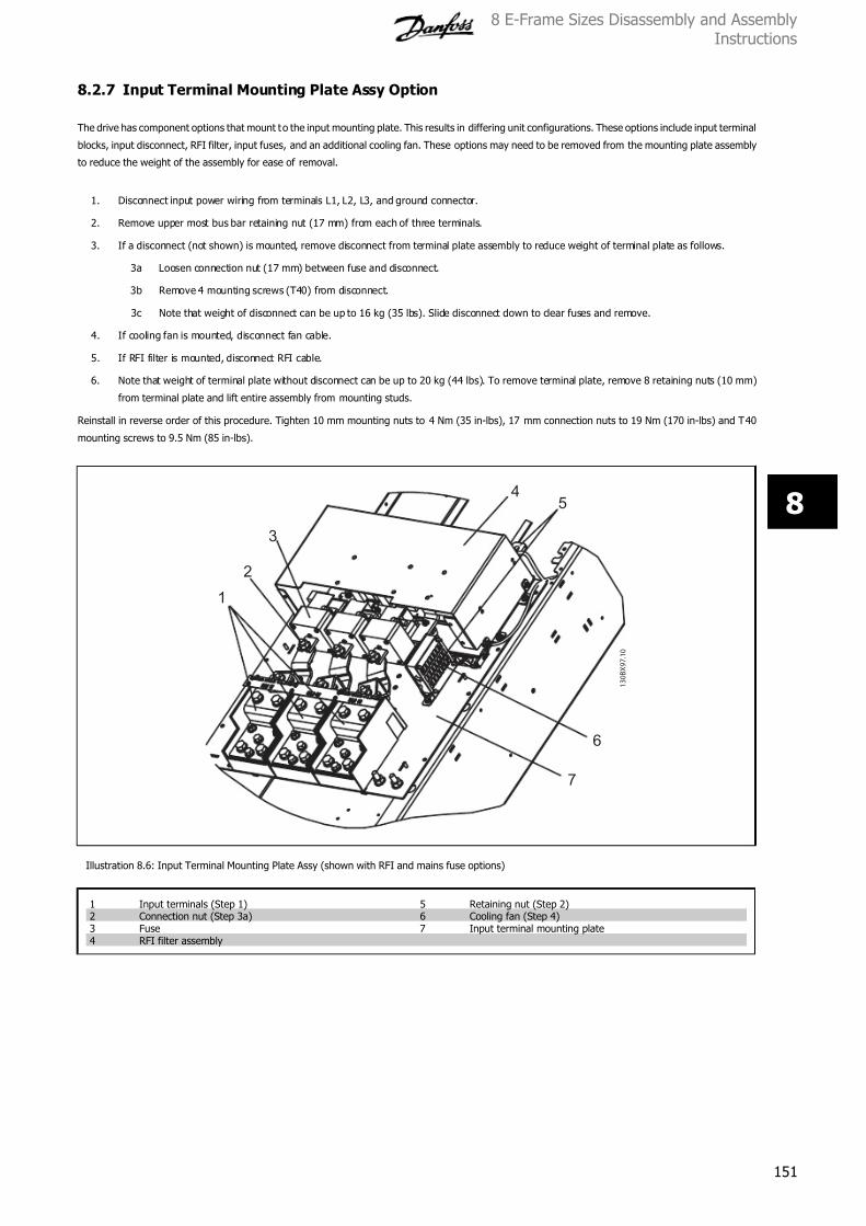
7/16/2019 1. D & E Frame.pdf
http://slidepdf.com/reader/full/1-d-e-framepdf 151/197
8.2.7 Input Terminal Mounting Plate Assy Option
The drive has component options that mount to the input mounting plate. This results in differing unit configurations. These options include input terminal
blocks, input disconnect, RFI filter, input fuses, and an additional cooling fan. These options may need to be removed from the mounting plate assembly
to reduce the weight of the assembly for ease of removal.
1. Disconnect input power wiring from terminals L1, L2, L3, and ground connector.
2. Remove upper most bus bar retaining nut (17 mm) from each of three terminals.
3. If a disconnect (not shown) is mounted, remove disconnect from terminal plate assembly to reduce weight of terminal plate as follows.
3a Loosen connection nut (17 mm) between fuse and disconnect.
3b Remove 4 mounting screws (T40) from disconnect.
3c Note that weight of disconnect can be up to 16 kg (35 lbs). Slide disconnect down to clear fuses and remove.
4. If cooling fan is mounted, disconnect fan cable.
5. If RFI filter is mounted, disconnect RFI cable.
6. Note that weight of terminal plate without disconnect can be up to 20 kg (44 lbs). To remove terminal plate, remove 8 retaining nuts (10 mm)
from terminal plate and lift entire assembly from mounting studs.
Reinstall in reverse order of this procedure. Tighten 10 mm mounting nuts to 4 Nm (35 in-lbs), 17 mm connection nuts to 19 Nm (170 in-lbs) and T40
mounting screws to 9.5 Nm (85 in-lbs).
1 3 0 B X 9 7 . 1 0
1
2
3
45
6
7
Illustration 8.6: Input Terminal Mounting Plate Assy (shown with RFI and mains fuse options)
1 Input terminals (Step 1) 5 Retaining nut (Step 2)2 Connection nut (Step 3a) 6 Cooling fan (Step 4)3 Fuse 7 Input terminal mounting plate4 RFI filter assembly
8 E-Frame Sizes Disassembly and AssemblyInstructions
151
8

7/16/2019 1. D & E Frame.pdf
http://slidepdf.com/reader/full/1-d-e-framepdf 152/197
8.2.8 Soft Charge Resistor
1. Remove input terminal plate assembly in accordance with procedure.
2. Disconnect MK4 connector on soft charge card.
3. Loosen top retaining nut (8 mm) on soft charge resistor.
4. Remove bottom retaining nut (8 mm) on soft charge resistor.
5. Lift bottom of soft charge resistor and remove resistor by sliding down.
Reinstall in reverse order of this procedure. Tighten 8 mm retaining nuts to 2.3 Nm (20 in-lbs).
1 3 0 B X 1 0 1 . 1 0
1 2
3
4
5
Illustration 8.7: Soft Charge Resistor
1 Soft charge card 4* Soft charge resistor2 MK4 connector (Step 2) 5 Bottom retaining nut (Step 4)3 Top retaining nut (Step 3)
*380-480/500V: Clear wire leads.
525-690V: Black wire leads.
8 E-Frame Sizes Disassembly and AssemblyInstructions
152
8
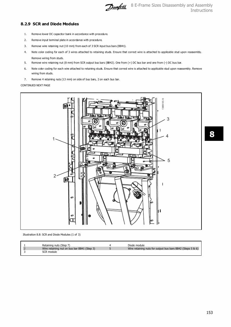
7/16/2019 1. D & E Frame.pdf
http://slidepdf.com/reader/full/1-d-e-framepdf 153/197
8.2.9 SCR and Diode Modules
1. Remove lower DC capacitor bank in accordance with procedure.
2. Remove input terminal plate in accordance with procedure.
3. Remove wire retaining nut (10 mm) from each of 3 SCR input bus bars (BB41).
4. Note color coding for each of 3 wires attached to retaining studs. Ensure that correct wire is attached to applicable stud upon reassembly.
Remove wiring from studs.
5. Remove wire retaining nut (8 mm) from SCR output bus bars (BB42). One from (+) DC bus bar and one from (–) DC bus bar.
6. Note color coding for each wire attached to retaining studs. Ensure that correct wire is attached to applicable stud upon reassembly. Remove
wiring from studs.
7. Remove 4 retaining nuts (13 mm) on side of bus bars, 2 on each bus bar.
CONTINUED NEXT PAGE
1 3 0 B X 1 0 5 . 1
0
1
2
3
4
5
Illustration 8.8: SCR and Diode Modules (1 of 3)
1 Retaining nuts (Step 7) 4 Diode module2 Wire retaining nut on bus bar BB41 (Step 3) 5 Wire retaining nuts for output bus bars BB42 (Steps 5 & 6)3 SCR module
8 E-Frame Sizes Disassembly and AssemblyInstructions
153
8

7/16/2019 1. D & E Frame.pdf
http://slidepdf.com/reader/full/1-d-e-framepdf 154/197
8. If unit is not equipped with load sharing option, proceed to step 9. If unit is equipped with load sharing, load share minus (-) bus bar must be
removed as follows.
8a. Remove 2 retaining nuts (13 mm) connecting load share bus bar to the SCR output bus bar.
8b. Remove retaining nut (17 mm) connecting load share bus bar to load share terminal on opposite end of bus bar (not shown).
8c. Remove load share bus bar.
9. Remove both positive (+) and negative (-) SCR output bus bars by removing 6 connection screws (T50). There are 3 screws per bus bar.
10. Remove three SCR and Diode input bus bars by removing 6 connection screws (T50). There are 2 screws per bus bar.
CONTINUED NEXT PAGE
1 3 0 B X 1 2 9 . 1 0
1
2
3
4
5
6
Illustration 8.9: SCR and Diode Modules (2 of 3)
1 Load sharing option retaining stud (Step 8) 4 Positive (+) output bus bar connecting screw (Step 9)2 SCR and Diode input bus bar BB41 (Step 10) 5 Negative (-) output bus bar BB42 (Step 9)3 Positive (+) output bus bar BB42 (Step 9) 6 Negative (-) output bus bar connecting screw (Step 9)
8 E-Frame Sizes Disassembly and AssemblyInstructions
154
8

7/16/2019 1. D & E Frame.pdf
http://slidepdf.com/reader/full/1-d-e-framepdf 155/197
11. Note which gate lead connects to each SCR module. Ensure that correct wire is attached to applicable SCR upon reassembly. Remove wiring
from each SCR modules. Connector is keyed for proper reinstallation. DO NOT force connection.
12. Remove SCR or diode module by removing 4 retaining screws (T25) from each module.
REASSEMBLY
Equipment Damage!
Do not reverse SCR and diode modules during installation. Reversing SCR and diode modules can result in equipment damage.
NB!
For each AC input phase there is one SCR module and one diode module. The SCR is on the left, diode on the right (as seen facing
upright unit). There are three pair. Only the SCR module has a connection pin for the gate signals.
1. Replace SCR and diode modules in accordance with instructions included with replacement modules.
2. Reassemble in reverse order.
Attaching Hardware Tightening Torque
T50 Per spare part instructionT25 Per spare part instruction17 mm 19 Nm (170 in-lbs)13 mm 9.5 Nm (85 in-lbs)
10 mm 4 Nm (35 in-lbs)8 mm 2.5 Nm (20 in-lbs)
1 3 0 B X 1 0 7 . 1 0
1
2
3
4
5 6 7
8
Illustration 8.10: SCR and Diode Modules (3 of 3)
1 SCR module SCR2 5 Diode module D12 Retaining screw (Step 12) 6 Diode module D23 SCR module SCR1 7 Diode module D34 SCR gate lead connection (Step 11) 8 SCR module SCR3
8 E-Frame Sizes Disassembly and AssemblyInstructions
155
8
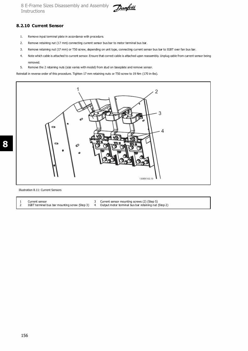
7/16/2019 1. D & E Frame.pdf
http://slidepdf.com/reader/full/1-d-e-framepdf 156/197
8.2.10 Current Sensor
1. Remove input terminal plate in accordance with procedure.
2. Remove retaining nut (17 mm) connecting current sensor bus bar to motor terminal bus bar.
3. Remove retaining nut (17 mm) or T50 screw, depending on unit type, connecting current sensor bus bar to IGBT over fan bus bar.
4. Note which cable is attached to current sensor. Ensure that correct cable is attached upon reassembly. Unplug cable from current sensor being
removed.
5. Remove the 2 retaining nuts (size varies with model) from stud on baseplate and remove sensor.
Reinstall in reverse order of this procedure. Tighten 17 mm retaining nuts or T50 screw to 19 Nm (170 in-lbs).
130BX102.10
1 2
3
4
Illustration 8.11: Current Sensors
1 Current sensor 3 Current sensor mounting screws (2) (Step 5)2 IGBT terminal bus bar mounting screw (Step 3) 4 Output motor terminal bus bar retaining nut (Step 2)
8 E-Frame Sizes Disassembly and AssemblyInstructions
156
8

7/16/2019 1. D & E Frame.pdf
http://slidepdf.com/reader/full/1-d-e-framepdf 157/197
8.2.11 Heatsink Fan Assembly
1. Remove input terminal plate in accordance with procedure.
2. Remove retaining nut (17 mm) or T50 Torx screw, depending on unit type, connecting each of 3 IGBT over-fan bus bars to 3 current sensor
bus bars.
3. Remove retaining nut (17 mm) connecting each of three IGBT over-fan bus bars to three IGBT output bus bars.
4. Disconnect in-line Molex connector in fan wiring. Cut tie wrap to free wiring from frame.
5. Remove fan assembly by removing 6 retaining nuts (10 mm). Note that fan assembly weights approximately 11 kg (25 pounds).
Reinstall in reverse order of this procedure. Tighten 10 mm retaining nuts to 4 Nm (35 in-lbs) and 17 mm connecting nuts or T50 screw to 19 Nm (170
in-lbs).
1 3 0 B X 1 0 3 . 1 0
3
2
1
6
5
4
Illustration 8.12: Fan Assembly
1 IGBT output bus bar BB49 4 Retaining nut (Step 3)2 Fan housing 5 Molex connector (Step 4)3 Retaining nut (Step 5) 6 Retaining nut (Step 2)
8 E-Frame Sizes Disassembly and AssemblyInstructions
157
8
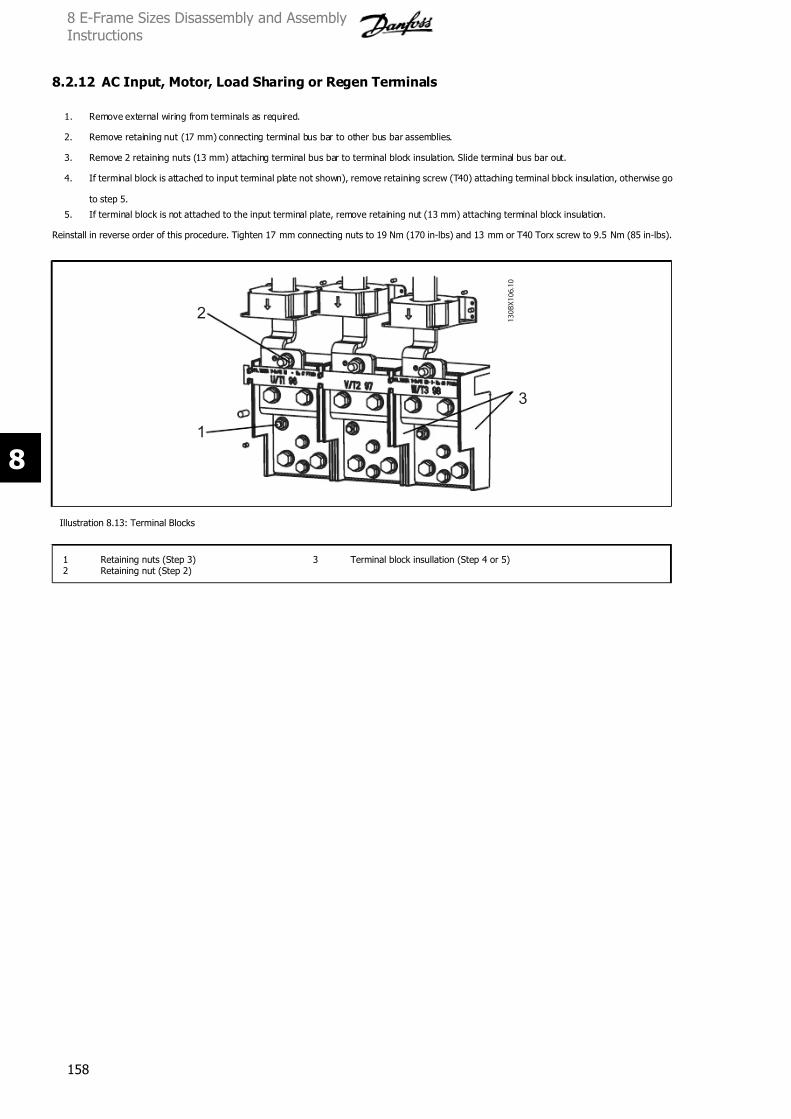
7/16/2019 1. D & E Frame.pdf
http://slidepdf.com/reader/full/1-d-e-framepdf 158/197
8.2.12 AC Input, Motor, Load Sharing or Regen Terminals
1. Remove external wiring from terminals as required.
2. Remove retaining nut (17 mm) connecting terminal bus bar to other bus bar assemblies.
3. Remove 2 retaining nuts (13 mm) attaching terminal bus bar to terminal block insulation. Slide terminal bus bar out.
4. If terminal block is attached to input terminal plate not shown), remove retaining screw (T40) attaching terminal block insulation, otherwise go
to step 5.
5. If terminal block is not attached to the input terminal plate, remove retaining nut (13 mm) attaching terminal block insulation.
Reinstall in reverse order of this procedure. Tighten 17 mm connecting nuts to 19 Nm (170 in-lbs) and 13 mm or T40 Torx screw to 9.5 Nm (85 in-lbs).
1 3 0 B X 1 0 6 . 1 0
1
2
3
Illustration 8.13: Terminal Blocks
1 Retaining nuts (Step 3) 3 Terminal block insullation (Step 4 or 5)2 Retaining nut (Step 2)
8 E-Frame Sizes Disassembly and AssemblyInstructions
158
8

7/16/2019 1. D & E Frame.pdf
http://slidepdf.com/reader/full/1-d-e-framepdf 159/197
8.2.13 IGBT Modules
1. Remove both DC capacitor banks in accordance with procedure.
2. Remove Input Terminal Plate in accordance with procedure.
3. Remove wire retaining nut (10 mm) from each of 3 SCR input bus bars.
4. Note color coding for each of 3 wires attached to retaining studs. Ensure that correct wire is attached to applicable stud upon reassembly.
Remove wiring from studs.
5. Remove wire retaining nut (8 mm) from SCR output bus bars. One from (+) DC bus bar and one from (–) DC bus bar.
6. Note color coding for each wire attached to retaining studs. Ensure that correct wire is attached to applicable stud upon reassembly. Remove
wiring from studs.
7. Remove 4 retaining nuts (13 mm) on side of bus bars, 2 on each bus bar.
CONTINUED NEXT PAGE
1 3 0 B X 1 3 0 . 1 0
1
2
3
4
Illustration 8.14: IGBT Modules (1 of 4)
1 Retaining nuts (Step 7) 3 IGBT board2 Wire retaining nut on bus bar BB41 (Step 3) 4 Wire retaining nuts for output bus bars BB42
(Steps 5 & 6)
8 E-Frame Sizes Disassembly and AssemblyInstructions
159
8

7/16/2019 1. D & E Frame.pdf
http://slidepdf.com/reader/full/1-d-e-framepdf 160/197
8. If unit is not equipped with load sharing option, proceed to step 9. If unit is equipped with load sharing, load share minus (-) bus bar must be
removed as follows.
8a.Remove 2 retaining nuts (13 mm) connecting load share bus bar to the SCR output bus bar.
8b.Remove retaining nut (17 mm) connecting load share bus bar to load share terminal on opposite end of bus bar (not shown).
8c.Remove load share bus bar.
9. Remove both positive (+) and negative (-) SCR output bus bars by removing 6 connection screws (T50). There are 3 screws per bus bar.
10. Remove three SCR and Diode input bus bars by removing 6 connection screws (T50). There are 2 screws per bus bar.
CONTINUED NEXT PAGE
1 3 0 B X 1 2 9 . 1 0
1
2
3
4
5
6
Illustration 8.15: IGBT Modules (2 of 4)
1 Load sharing option retaining studs (Step 8) 4 Positive (+) output bus bar connecting screw (Step 9)2 SCR and Diode input bus bar BB41 (Step 10) 5 Negative (-) output bus bar BB42 (Step 9)3 Positive (+) output bus bar BB42 (Step 9) 6 Negative (-) output bus bar connecting screw (Step 9)
8 E-Frame Sizes Disassembly and AssemblyInstructions
160
8
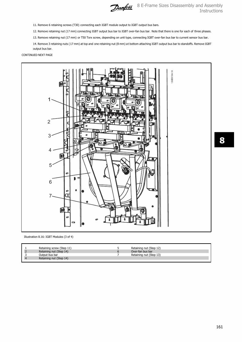
7/16/2019 1. D & E Frame.pdf
http://slidepdf.com/reader/full/1-d-e-framepdf 161/197
11. Remove 6 retaining screws (T30) connecting each IGBT module output to IGBT output bus bars.
12. Remove retaining nut (17 mm) connecting IGBT output bus bar to IGBT over-fan bus bar. Note that there is one for each of three phases.
13. Remove retaining nut (17 mm) or T50 Torx screw, depending on unit type, connecting IGBT over-fan bus bar to current sensor bus bar.
14. Remove 3 retaining nuts (17 mm) at top and one retaining nut (8 mm) at bottom attaching IGBT output bus bar to standoffs. Remove IGBT
output bus bar.
CONTINUED NEXT PAGE
1 3 0 B X 1 0 4 . 1 0
1
2
3
4
5
1
6
7
Illustration 8.16: IGBT Modules (3 of 4)
1 Retaining screw (Step 11) 5 Retaining nut (Step 12)2 Retaining nut (Step 14) 6 Over-fan bus bar3 Output bus bar 7 Retaining nut (Step 13)4 Retaining nut (Step 14)
8 E-Frame Sizes Disassembly and AssemblyInstructions
161
8
7/16/2019 1. D & E Frame.pdf
http://slidepdf.com/reader/full/1-d-e-framepdf 162/197
15. Remove 18 retaining screws (T30) on IGBT input terminals. Note snubber capacitors come off when screws are removed. There are 6 screws
for each IGBT module.
16. Remove 2 retaining nuts (8 mm) connecting each IGBT-Cap bus bar assemblies to IGBT-Ind bus bar assembly and remove the IGBT-Cap
bus bar assembly. There are three IGBT-Cap bus bar assemblies.
17. Remove retaining nut (8 mm) from high frequency board.
18. Remove 2 retaining screws (T25) f rom high frequency board.
19. Disconnect wire assembly from high frequency board and remove board.
20. If unit has Brake IGBTs, remove the 4 retaining screws (T30) connecting IGBT-Ind bus bar assembly to Brake IGBT. Note that there are 2
screws per Brake IGBT module.
21. Remove 4 retaining nuts (13 mm) connecting IGBT-Ind bus bar assembly to two DC bus bars from inductor. Remove IGBT-Ind bus bar
assembly.
22. Remove 8 retaining screws (T25) mounting each IGBT module.
REASSEMBLY
1. Replace IGBT modules in accordance with instructions included with replacement modules.
2. Reassemble in reverse order.
Attaching Hardware Tightening Torque
8 mm / T25 2.5 Nm (20 in-lbs)10 mm / T30 4 Nm (35 in-lbs)13 mm 9.5 Nm (85 in-lbs)17 mm / T50 19 Nm (170 in-lbs)
8 E-Frame Sizes Disassembly and AssemblyInstructions
162
8

7/16/2019 1. D & E Frame.pdf
http://slidepdf.com/reader/full/1-d-e-framepdf 163/197
130BX131.10
1
2
3
4
5
6
7
8
9
10
11
Illustration 8.17: IGBT Modules (4 of 4)
1 Snubber capacitor 7 Retaining screw (Step 16)2 Retaining screw (brake IGBT option) (Step 20) 8 Retaining screw (Step 15)3 Retaining nut (Step 17) 9 IGBT-Cap bus bar BB474 Retaining nut (Step 21) 10 IGBT board5 High Frequency board 11 IGBT retaining screw (Step 22)6 Retaining screw (Step 18)
8 E-Frame Sizes Disassembly and AssemblyInstructions
163
8

7/16/2019 1. D & E Frame.pdf
http://slidepdf.com/reader/full/1-d-e-framepdf 164/197
9 Special Test Equipment
164
9
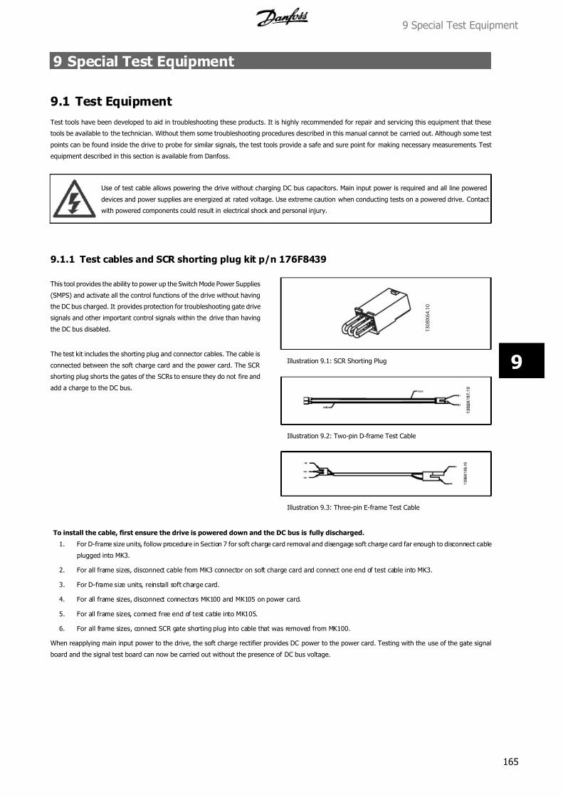
7/16/2019 1. D & E Frame.pdf
http://slidepdf.com/reader/full/1-d-e-framepdf 165/197
9 Special Test Equipment
9.1 Test Equipment
Test tools have been developed to aid in troubleshooting these products. It is highly recommended for repair and servicing this equipment that these
tools be available to the technician. Without them some troubleshooting procedures described in this manual cannot be carried out. Although some test
points can be found inside the drive to probe for similar signals, the test tools provide a safe and sure point for making necessary measurements. Test
equipment described in this section is available from Danfoss.
Use of test cable allows powering the drive without charging DC bus capacitors. Main input power is required and all line powered
devices and power supplies are energized at rated voltage. Use extreme caution when conducting tests on a powered drive. Contact
with powered components could result in electrical shock and personal injury.
9.1.1 Test cables and SCR shorting plug kit p/n 176F8439
This tool provides the ability to power up the Switch Mode Power Supplies
(SMPS) and activate all the control functions of the drive without having
the DC bus charged. It provides protection for troubleshooting gate drive
signals and other important control signals within the drive than having
the DC bus disabled.
The test kit includes the shorting plug and connector cables. The cable is
connected between the soft charge card and the power card. The SCR
shorting plug shorts the gates of the SCRs to ensure they do not fire and
add a charge to the DC bus.
1 3 0 B X 6 4 . 1 0
Illustration 9.1: SCR Shorting Plug
Illustration 9.2: Two-pin D-frame Test Cable
Illustration 9.3: Three-pin E-frame Test Cable
To install the cable, first ensure the drive is powered down and the DC bus is fully discharged.
1. For D-frame size units, follow procedure in Section 7 for soft charge card removal and disengage soft charge card far enough to disconnect cable
plugged into MK3.
2. For all frame sizes, disconnect cable from MK3 connector on soft charge card and connect one end of test cable into MK3.
3. For D-frame size units, reinstall soft charge card.
4. For all frame sizes, disconnect connectors MK100 and MK105 on power card.
5. For all frame sizes, connect free end of test cable into MK105.
6. For all frame sizes, connect SCR gate shorting plug into cable that was removed from MK100.
When reapplying main input power to the drive, the soft charge rectifier provides DC power to the power card. Testing with the use of the gate signal
board and the signal test board can now be carried out without the presence of DC bus voltage.
9 Special Test Equipment
165
9
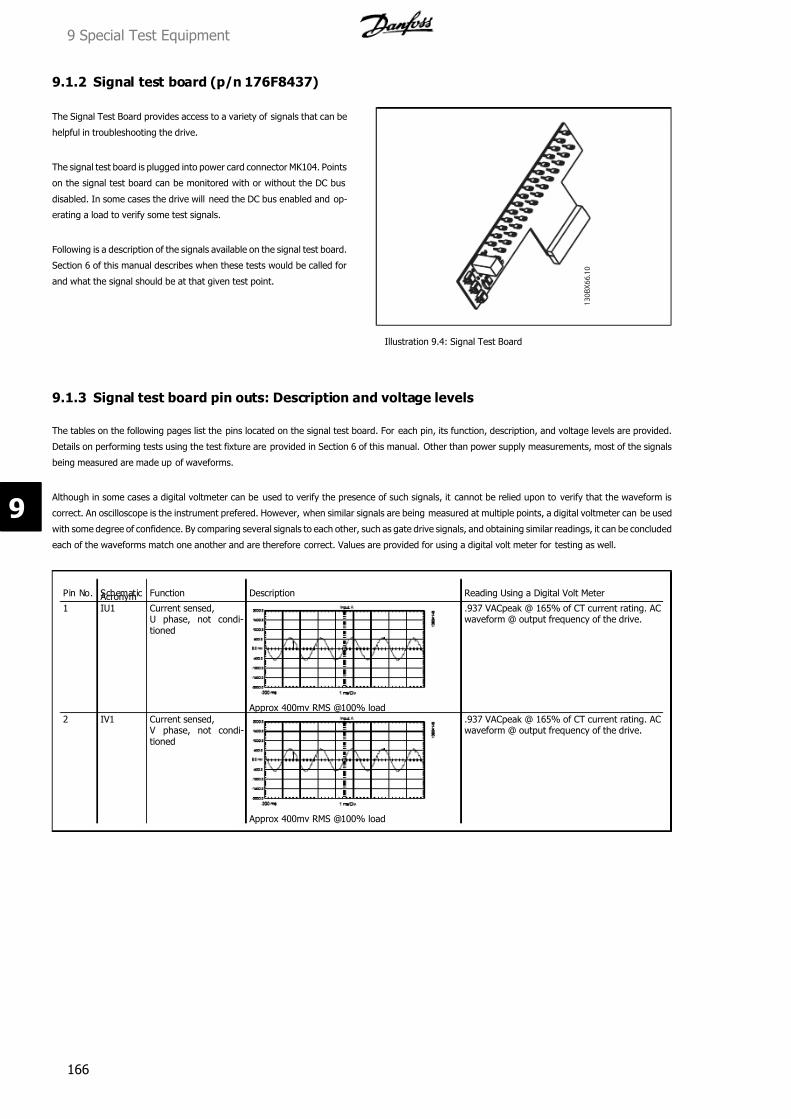
7/16/2019 1. D & E Frame.pdf
http://slidepdf.com/reader/full/1-d-e-framepdf 166/197
9.1.2 Signal test board (p/n 176F8437)
The Signal Test Board provides access to a variety of signals that can be
helpful in troubleshooting the drive.
The signal test board is plugged into power card connector MK104. Points
on the signal test board can be monitored with or without the DC bus
disabled. In some cases the drive will need the DC bus enabled and op-
erating a load to verify some test signals.
Following is a description of the signals available on the signal test board.
Section 6 of this manual describes when these tests would be called for
and what the signal should be at that given test point.
1 3 0 B X 6 6 . 1 0
Illustration 9.4: Signal Test Board
9.1.3 Signal test board pin outs: Description and voltage levels
The tables on the following pages list the pins located on the signal test board. For each pin, its function, description, and voltage levels are provided.
Details on performing tests using the test fixture are provided in Section 6 of this manual. Other than power supply measurements, most of the signals
being measured are made up of waveforms.
Although in some cases a digital voltmeter can be used to verify the presence of such signals, it cannot be relied upon to verify that the waveform is
correct. An oscilloscope is the instrument prefered. However, when similar signals are being measured at multiple points, a digital voltmeter can be used
with some degree of confidence. By comparing several signals to each other, such as gate drive signals, and obtaining similar readings, it can be concluded
each of the waveforms match one another and are therefore correct. Values are provided for using a digital volt meter for testing as well.
Pin No. Schematic Acronym Function Description Reading Using a Digital Volt Meter
1 IU1 Current sensed,U phase, not condi-tioned
Approx 400mv RMS @100% load
.937 VACpeak @ 165% of CT current rating. ACwaveform @ output frequency of the drive.
2 IV1 Current sensed, V phase, not condi-tioned
Approx 400mv RMS @100% load
.937 VACpeak @ 165% of CT current rating. ACwaveform @ output frequency of the drive.
9 Special Test Equipment
166
9

7/16/2019 1. D & E Frame.pdf
http://slidepdf.com/reader/full/1-d-e-framepdf 167/197
Pin No. Schematic Acronym
Function Description Reading Using a Digital Volt Meter
3 IW1 Current sensed,W phase, not condi-tioned
Approx 400mv RMS @100% load
.937 VACpeak @ 165% of CT current rating. ACwaveform @ output frequency of the drive.
4 COMMON Logic common This common is for all signals.
5 AMBT Ambient temp. Used to control FAN high and low fan speeds. 1 VDC approximately equal to 25C
6 FANO Control Card signal Signal from Control Card to turn fans on and off. 0 VDC – ON command
5 VDC – OFF command
7 INRUSH Control Card signal Signal f rom Control Card to start gating SCR frontend
5 VDC – SCRs disabled
0 VDC – SCRs enabled
8 RL1 Control Card signal Signal from Control Card to provide status of Relay01
0 VDC – Relay active
0.7 VDC – inactive
9 Not used
10 Not used
11 VPOS +18 VDC regulated
supply +16.5 to 19.5 VDC
Red LED indicates voltage is present between VPOS
and VNEG terminals.
+18 VDC regulated supply +16.5 to 19.5 VDC
12 VNEG -18 VDC regulated sup-ply
-16.5 to 19.5 VDC
Red LED indicates voltage is present between VPOSand VNEG terminals.
-18 VDC regulated supply-16.5 to 19.5 VDC
13 DBGATE Brake IGBT gate pulsetrain
Varies w/ brake duty cycle
Voltage drops to zero when brake is turned off. Voltage increases to 4.04 VDC as brake duty cy-cle reaches max.
14 BRT_ON Brake IGBT 5V logiclevel signal.
Varies w/ brake duty cycle
5.10 VDC level with the brake turned off. Voltagedecreases to zero as brake duty cycle reachesmax.
15 Not used
16 FAN_TST Control signal for fans Indicates Fan Test switch is activated to force thefans on high
+5VDC – disabled
0VDC – fans on high
17 FAN_ON Pulse train to gateSCR’s for fan voltagecontrol. In sync withline freq.
7 trigger pulses at 3Khz
5VDC - fans off
18 HI_LOW Control signal from
Power Card
Signal to switch fan speeds between high and low +5VDC = fans on high,
Otherwise 0VDC.19 SCR_DIS Control signal for SCR
front endIndicates SCR front end is enabled or disabled. 0.6 to 0.8 VDC – SCRs enabled
0VDC – SCR disabled
20 INV_DIS Control signal fromPower Card
Disables IGBT gate voltages 5VDC – inverter disabled
0VDC – inverter enabled
21 Not used
22 UINVEX Bus Voltage scaleddown
Signal proportional to UDC 1VDC = 262 VDC OV switch must be off.
23 VDD +24 VDC power supply Yellow LED indicates voltage is present. +24 VDC regulated supply
+23 to 25 VDC
24 VCC +5.0 VDC regulatedsupply. +4.75-5.25
VDC
Green LED indicates voltage is present. +5.0 VDC regulated supply +4.75 to 5.25 VDC
9 Special Test Equipment
167
9

7/16/2019 1. D & E Frame.pdf
http://slidepdf.com/reader/full/1-d-e-framepdf 168/197
Pin No. Schematic Acronym
Function Description Reading Using a Digital Volt Meter
25 GUP_T IGBT gate signal, buf-fered, U phase, posi-tive. Signal originateson Control Card.
2v/div 100us/div Run@10Hz
2.2 - 2.5 VDCEqual on all phasesTP25-TP30
26 GUN_T IGBT gate signal, buf-fered, U phase, nega-tive. Signal originateson Control Card.
2v/div 100us/div Run@10Hz
2.2 - 2.5 VDCEqual on all phasesTP25-TP30
27 GVP_T IGBT gate signal, buf-fered, V phase, posi-tive. Signal originateson Control Card.
2v/div 100us/div Run@10Hz
2.2 - 2.5 VDCEqual on all phasesTP25-TP30
28 GVN_T IGBT gate signal, buf-fered, V phase, nega-tive. Signal originateson Control Card.
2v/div 100us/div Run@10Hz
2.2 - 2.5 VDCEqual on all phasesTP25-TP30
29 GWP_T IGBT gate signal, buf-fered, W phase, posi-tive. Signal originates
on Control Card.
2v/div 100us/div Run@10Hz
2.2 - 2.5 VDCEqual on all phasesTP25-TP30
30 GWN_T IGBT gate signal, buf-fered, W phase, nega-tive. Signal originateson Control Card.
2v/div 100us/div Run@10Hz
2.2 - 2.5 VDCEqual on all phases TP25-TP30
9 Special Test Equipment
168
9

7/16/2019 1. D & E Frame.pdf
http://slidepdf.com/reader/full/1-d-e-framepdf 169/197
10 Spare Parts List
10.1 Spare Parts List
10.1.1 General Notes
General Notes:
All spare parts are suitable for conformal coated drives and can be used in either coated or non-conformal coated drives.
Bus bars used in some units are aluminum. Spare part bus bars are always plated copper. Plated copper bus bars are useable for all units.
For the latest spare parts list, visit the Danfoss website at www.danfoss-
drives.com
10 Spare Parts List
169
10
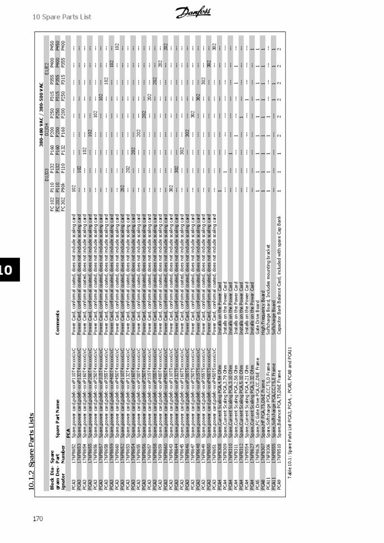
7/16/2019 1. D & E Frame.pdf
http://slidepdf.com/reader/full/1-d-e-framepdf 170/197

7/16/2019 1. D & E Frame.pdf
http://slidepdf.com/reader/full/1-d-e-framepdf 171/197

7/16/2019 1. D & E Frame.pdf
http://slidepdf.com/reader/full/1-d-e-framepdf 172/197
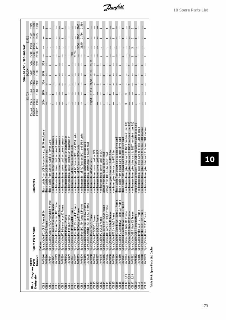
7/16/2019 1. D & E Frame.pdf
http://slidepdf.com/reader/full/1-d-e-framepdf 173/197
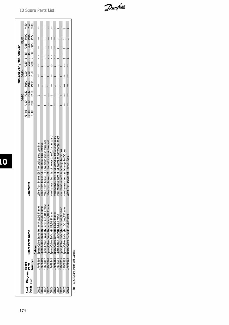
7/16/2019 1. D & E Frame.pdf
http://slidepdf.com/reader/full/1-d-e-framepdf 174/197
3 8 0 - 4 8 0 V A C / 3 8 0 - 5 0 0 V A C
D 1 / D 3
D 2 / D 4
E 1 / E 2
B l o c k
D i a g r a m
D e s i g n
a t o r
S p a r e
P a r t s
N u m b e r
S p a r e P a r t s N a m e
C o m m e n t s
F C 1
0 2
P 1 1 0
P 1 3 2
P 1 6 0
P 2 0 0
P 2 5 0
P 3
1 5
P 3 5 5
P 4 0 0
P 4 5 0
F C 2
0 2
P 1 1 0
P 1 3 2
P 1 6 0
P 2 0 0
P 2 5 0
P 3
1 5
P 3 5 5
P 4 0 0
P 4 5 0
F C 3
0 2
P 9 0 K
P 1 1 0
P 1 3 2
P 1 6 0
P 2 0 0
P 2
5 0
P 3 1 5
P 3 5 5
P 4 0 0
C a b l e s
C B L 2 2
1 7 6 F 8 3 6 6
S p a r e , C a b l e , B r a k e P o w
e r P l u s , D 1 F r a m e
c a b l e f r o m b r a k e I G B T t o b r a k e p l u s t e r m i n a l
1
1
- - -
- - -
- - -
- - -
- - -
- - -
- - -
C B L 2 2
1 7 6 F 8 3 6 9
S p a r e , C a b l e , B r a k e P o w
e r P l u s , D 2 F r a m e
c a b l e f r o m b r a k e I G B T
t o b r a k e p l u s t e r m i n a l
- - -
- - -
1
1
1
- - -
- - -
- - -
- - -
C B L 2 3
1 7 6 F 8 3 6 7
S p a r e , C a b l e , B r a k e P o w
e r M i n u s , D 1 F r a m e
c a b l e f r o m b r a k e I G B T t o b r a k e m i n u s t e r m i n a l
1
1
- - -
- - -
- - -
- - -
- - -
- - -
- - -
C B L 2 3
1 7 6 F 8 3 7 0
S p a r e , C a b l e , B r a k e P o w
e r M i n u s , D 2 F r a m e
c a b l e f r o m b r a k e I G B T
t o b r a k e m i n u s t e r m i n a l
- - -
- - -
1
1
1
- - -
- - -
- - -
- - -
C B L 2 4
1 7 6 F 8 5 4 3
S p a r e , C a b l e , S o f t c h g R S T , D
1 F r a m e
w i r e h a r n e s s f r o m i n p u t p o w e r t o s o f t c h a r g e b o a r d
1
1
- - -
- - -
- - -
- - -
- - -
- - -
- - -
C B L 2 4
1 7 6 F 8 3 5 3
S p a r e , C a b l e , S o f t c h g R S T , D
2 F r a m e
w i r e h a r n e s s f r o m i n p u t p o w e r t o s o f t c h a r g e b o a r d
- - -
- - -
1
1
1
- - -
- - -
- - -
- - -
C B L 2 4
1 7 6 F 8 5 8 4
S p a r e , C a b l e , S o f t c h g R S T , E
F r a m e
w i r e h a r n e s s f r o m i n p u t p o w e r t o s o f t c h a r g e b o a r d
- - -
- - -
- - -
- - -
- - -
1
1
1
1
C B L 2 5
1 7 6 F 8 3 5 5
S p a r e , C a b l e , S o f t c h g t o
D C b u s , D F r a m e
w i r e h a r n e s s f r o m s o f t c h a r g e t o D C b u s
1
1
1
1
1
- - -
- - -
- - -
- - -
C B L 2 5
1 7 6 F 8 5 8 5
S p a r e , C a b l e , S o f t c h g t o
D C b u s , E F r a m e
w i r e h a r n e s s f r o m s o f t c h a r g e t o D C b u s
- - -
- - -
- - -
- - -
- - -
1
1
1
1
C B L 2 6
1 7 6 F 8 6 1 3
S p a r e , C a b l e , F
C F u s e F a n , E
F r a m e
c a b l e f r o m p o w e r c a r d
t o f a n f u s e
- - -
- - -
- - -
- - -
- - -
1
1
1
1
T a b l e
1 0 . 5 : S p a r e P a r t s L i s t C a b l e s
10 Spare Parts List
174
10
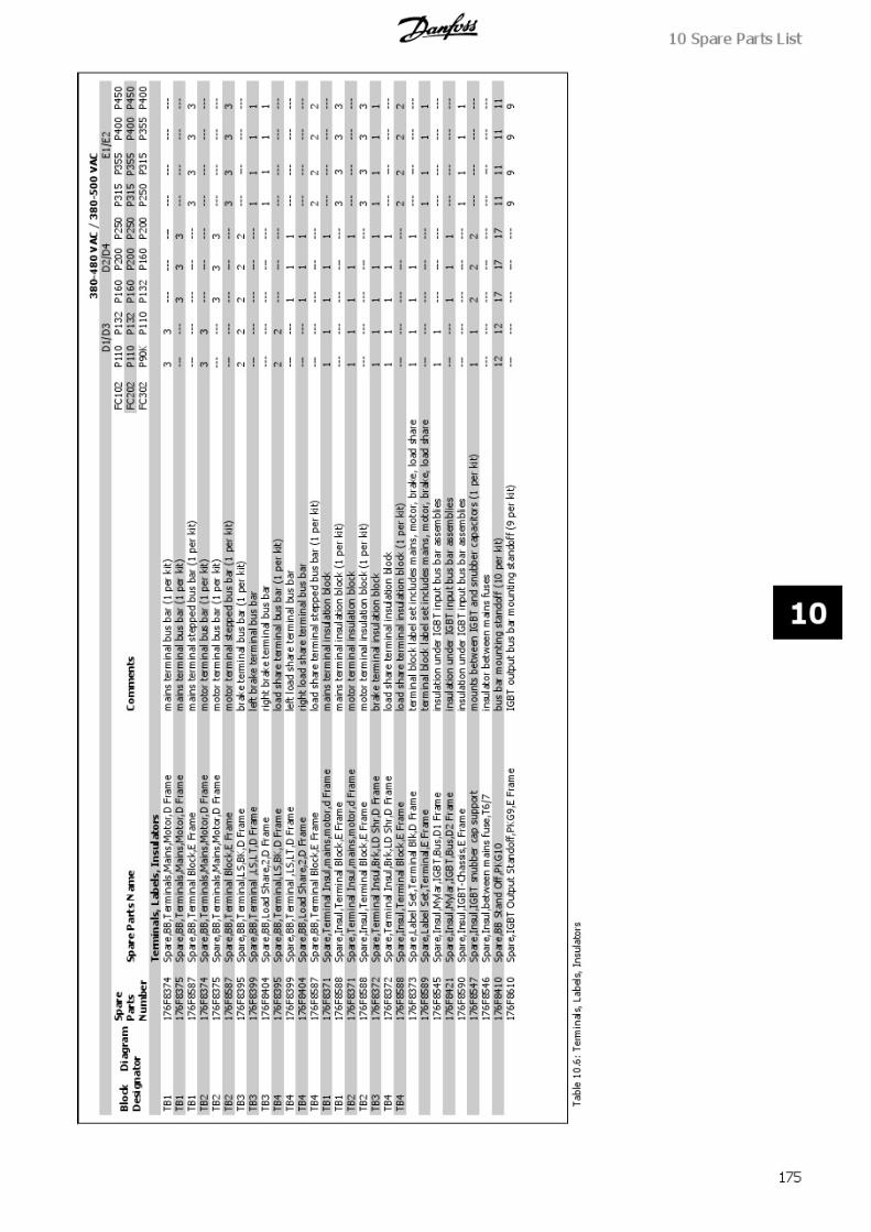
7/16/2019 1. D & E Frame.pdf
http://slidepdf.com/reader/full/1-d-e-framepdf 175/197

7/16/2019 1. D & E Frame.pdf
http://slidepdf.com/reader/full/1-d-e-framepdf 176/197

7/16/2019 1. D & E Frame.pdf
http://slidepdf.com/reader/full/1-d-e-framepdf 177/197
3 8 0 - 4 8 0 V A C / 3 8 0 - 5 0 0 V A C
D 1 / D 3
D 2 / D 4
E 1 / E 2
B l o c k
D i a g r a m
D e s i g n
a t o r
S p a r e
P a r t s
N u m b e r
S p a r e P a r t s N a m e
C o m m e n t s
F C 1 0 2
P 1 1 0
P 1 3 2
P 1 6 0
P 2 0 0
P 2 5 0
P 3 1 5
P 3 5 5
P 4 0 0
P 4 5 0
F C 2 0 2
P 1 1 0
P 1 3 2
P 1 6 0
P 2 0 0
P 2 5 0
P 3 1 5
P 3 5 5
P 4 0 0
P 4 5 0
F C 3 0 2
P 9 0 K
P 1 1 0
P 1 3 2
P 1 6 0
P 2 0 0
P 2 5 0
P 3 1 5
P 3 5 5
P 4 0 0
B u s B a r s
1 7 6 F 8 4 0 1
S p a r e , B
B , L
S , P
l u s , D F r
a m e
c o n n e c t s p l u s l o a d
s h a r e t e r m i n a l t o S C R o u t p u t b u s b a r a s s e m b l y
1
1
- - -
- - -
- - -
- - -
- - -
- - -
- - -
1 7 6 F 8 4 0 0
S p a r e , B
B , L
S , M
i n u s , D F r a m e
c o n n e c t s m i n u s l o a d s h a r e t e r m i n a l t o S C R o u t p u t b u s b a r a s s e m b l y
1
1
- - -
- - -
- - -
- - -
- - -
- - -
- - -
1 7 6 F 8 4 0 3
S p a r e , B
B , L
S , P
l u s , D F r
a m e
c o n n e c t s S C R b u s
b a r t o p l u s l o a d s h a r e t e r m i n a l
- - -
- - -
1
1
1
- - -
- - -
- - -
- - -
1 7 6 F 8 4 0 2
S p a r e , B
B , L
S , M
i n u s , D F r a m e
c o n n e c t s S C R b u s
b a r t o m i n u s l o a d s h a r e t e r m i n a l
- - -
- - -
1
1
1
- - -
- - -
- - -
- - -
1 7 6 F 8 6 0 7
S p a r e , B
B , L o a d S h a r e P l u s , E F r a m e
l o a d s h a r e p l u s b u
s b a r
- - -
- - -
- - -
- - -
- - -
1
1
1
1
1 7 6 F 8 6 0 8
S p a r e , B
B , L o a d S h a r e M i n u s , E F r a m e
l o a d s h a r e m i n u s b u s b a r
- - -
- - -
- - -
- - -
- - -
1
1
1
1
1 7 6 F 8 4 0 5
S p a r e , B
B , S
C R , I n p u t 2
, D F r a m e
l o c a t e d o n i n p u t p
l a t e ( 1 p e r k i t )
3
3
- - -
- - -
- - -
- - -
- - -
- - -
- - -
1 7 6 F 8 4 0 6
S p a r e , B
B , S
C R , T , 1 , D F
r a m e
l o c a t e d o n i n p u t p
l a t e ( 1 p e r k i t )
- - -
- - -
3
3
3
- - -
- - -
- - -
- - -
1 7 6 F 8 4 0 7
S p a r e , B
B , D
i s c , D
F r a m
e
l o c a t e d o n i n p u t p
l a t e ( 1 p e r k i t )
3
3
- - -
- - -
- - -
- - -
- - -
- - -
- - -
1 7 6 F 8 4 0 8
S p a r e , B
B , D
i s c , R , S , D F
r a m e
l o c a t e d o n i n p u t p
l a t e ( 1 p e r k i t )
- - -
- - -
2
2
2
- - -
- - -
- - -
- - -
1 7 6 F 8 4 0 9
S p a r e , B
B , D
i s c , T , D
F r a
m e
l o c a t e d o n i n p u t p
l a t e ( 1 p e r k i t )
- - -
- - -
1
1
1
- - -
- - -
- - -
- - -
10 Spare Parts List
177
10

7/16/2019 1. D & E Frame.pdf
http://slidepdf.com/reader/full/1-d-e-framepdf 178/197
3 8 0 - 4 8 0 V A C / 3 8 0 - 5 0 0 V A C
D 1 / D 3
D 2 / D 4
E 1 / E 2
B l o c k
D i a g r a m
D e s i g n
a t o r
S p a r e
P a r t s
N u m b e r
S p a r e P a r t s N a m e
C o m m e n t s
F C 1 0 2
P 1 1 0
P 1 3 2
P 1 6 0
P 2 0 0
P 2 5 0
P 3 1 5
P 3 5 5
P 4 0 0
P 4 5 0
F C 2 0 2
P 1 1 0
P 1 3 2
P 1 6 0
P 2 0 0
P 2 5 0
P 3 1 5
P 3 5 5
P 4 0 0
P 4 5 0
F C 3 0 2
P 9 0 K
P 1 1 0
P 1 3 2
P 1 6 0
P 2 0 0
P 2 5 0
P 3 1 5
P 3 5 5
P 4 0 0
E n c l o s u r e
1 7 6 F 8 4 3 0
S p a r e , C a b l e C l a m p , 6 0
m m
6 0 m m p o w e r
c a b l e c l a m p
- - -
- - -
- - -
- - -
- - -
- - -
- - -
- - -
- - -
1 7 6 F 8 4 9 0
S p a r e , B r k t , H F , b o a r d , g
n d , D
F r a m e
m o u n t i n g b r a c
k e t f o r h i g h f r e q u e n c y b o a r d
1
1
- - -
- - -
- - -
- - -
- - -
- - -
- - -
1 7 6 F 8 4 9 1
S p a r e , B r k t , H F , b o a r d , g
n d , D
F r a m e
m o u n t i n g b r a c
k e t f o r h i g h f r e q u e n c y b o a r d
- - -
- - -
1
1
1
- - -
- - -
- - -
- - -
1 7 6 F 8 4 2 7
I P 0 0 ,
D 3 ,
S i d e P a n e l
I P 0 0
I P 0 0
1 7 6 F 8 4 2 8
I P 0 0 ,
D 4 ,
S i d e P a n e l
I P 0 0
I P 0 0
I P 0 0
10 Spare Parts List
178
10

7/16/2019 1. D & E Frame.pdf
http://slidepdf.com/reader/full/1-d-e-framepdf 179/197
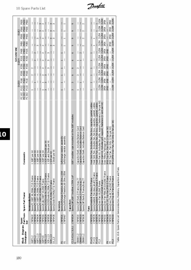
7/16/2019 1. D & E Frame.pdf
http://slidepdf.com/reader/full/1-d-e-framepdf 180/197
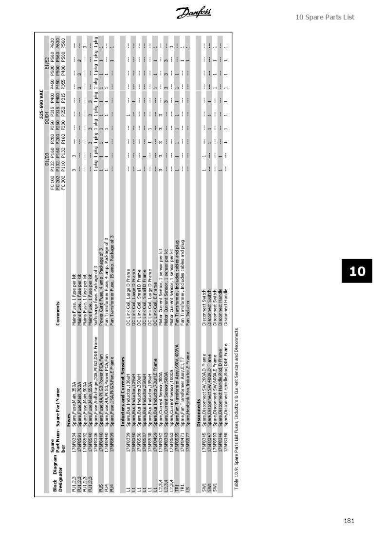
7/16/2019 1. D & E Frame.pdf
http://slidepdf.com/reader/full/1-d-e-framepdf 181/197

7/16/2019 1. D & E Frame.pdf
http://slidepdf.com/reader/full/1-d-e-framepdf 182/197

7/16/2019 1. D & E Frame.pdf
http://slidepdf.com/reader/full/1-d-e-framepdf 183/197
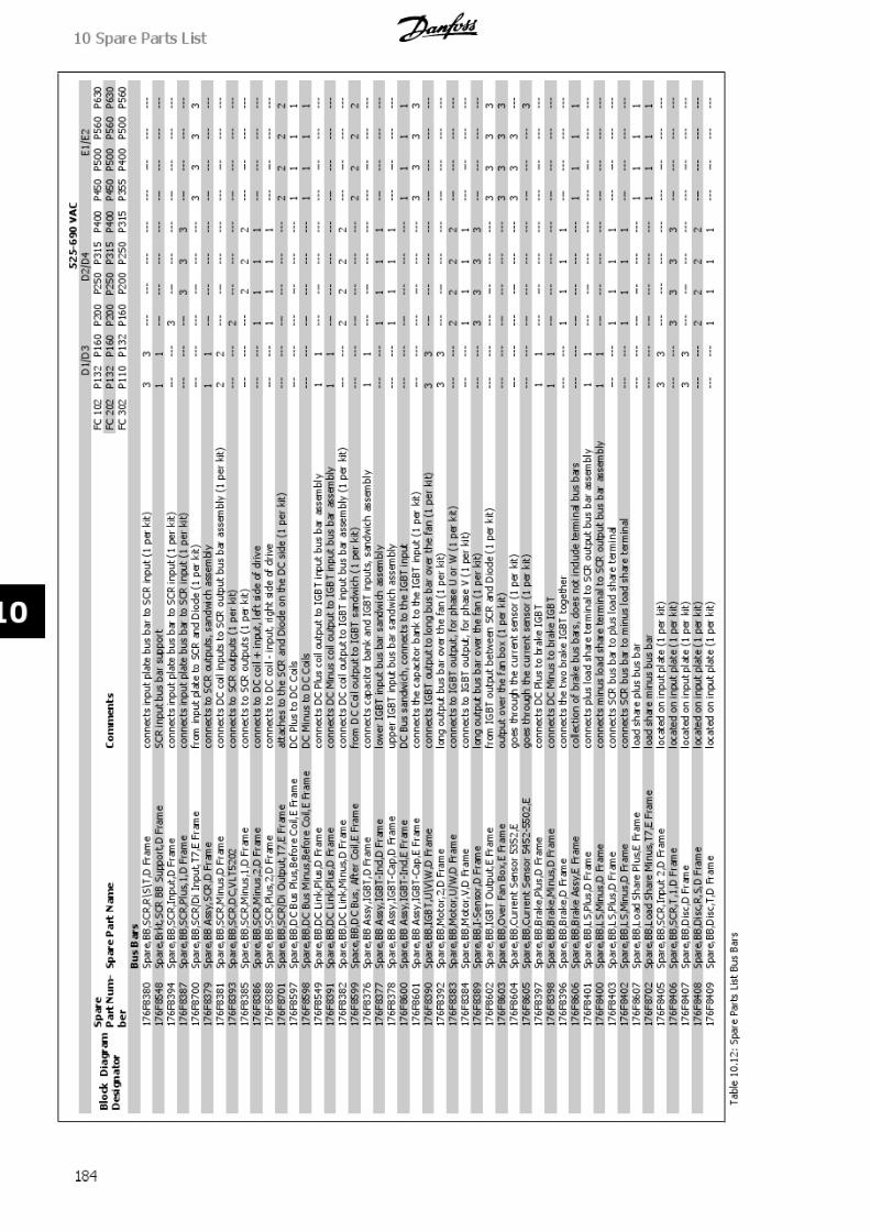
7/16/2019 1. D & E Frame.pdf
http://slidepdf.com/reader/full/1-d-e-framepdf 184/197

7/16/2019 1. D & E Frame.pdf
http://slidepdf.com/reader/full/1-d-e-framepdf 185/197
5 2 5 - 6 9 0 V A
C
D 1 / D 3
D 2 / D 4
E 1 / E 2
B l o c k
D i a g r a m
D e s i g n
a t o r
S p a r e
P a r t N u m -
b e r
S p a r e P a r t N a m e
C o m m e n t s
F C 1 0 2
P 1 3 2
P 1 6 0
P 2 0 0
P 2 5 0
P 3 1 5
P 4 0 0
P 4 5 0
P 5 0 0
P 5 6 0
P 6 3 0
F C 2 0 2
P 1 3 2
P 1 6 0
P 2 0 0
P 2 5 0
P 3 1 5
P 4 0 0
P 4 5 0
P 5 0 0
P 5 6 0
P 6 3 0
F C 3 0 2
P 1 1 0
P 1 3 2
P 1 6 0
P 2 0 0
P 2 5 0
P 3 1 5
P 3 5 5
P 4 0 0
P 5 0 0
P 5 6 0
E n c l o s u r e
1 7 6 F 8 4 3 0
S p a r e , C a b l e C l a m p , 6 0
m m
6 0 m m p o w e r c a b l e
c l a m p
- - -
- - -
- - -
- - -
- - -
- - -
- - -
- - -
- - -
- - -
1 7 6 F 8 4 9 0
S p a r e , B r k t , H F , b o a r d , g n d , D
F r a m e
m o u n t i n g b r a c k e t f o
r h i g h f r e q u e n c y b o a r d
1
1
- - -
- - -
- - -
- - -
- - -
- - -
- - -
- - -
1 7 6 F 8 4 9 1
S p a r e , B r k t , H F , b o a r d , g n d , D
F r a m e
m o u n t i n g b r a c k e t f o
r h i g h f r e q u e n c y b o a r d
- - -
- - -
1
1
1
1
- - -
- - -
- - -
- - -
1 7 6 F 8 4 2 7
I P 0 0 ,
D 3 ,
S i d e P a n e l
I P 0 0
I P 0 0
1 7 6 F 8 4 2 8
I P 0 0 ,
D 4 ,
S i d e P a n e l
I P 0 0
I P 0 0
I P 0 0
I P 0 0
T a b l e
1 0 . 1
3 : S p a r e P a r t s L i s t E n c l o s u r e
10 Spare Parts List
185
10
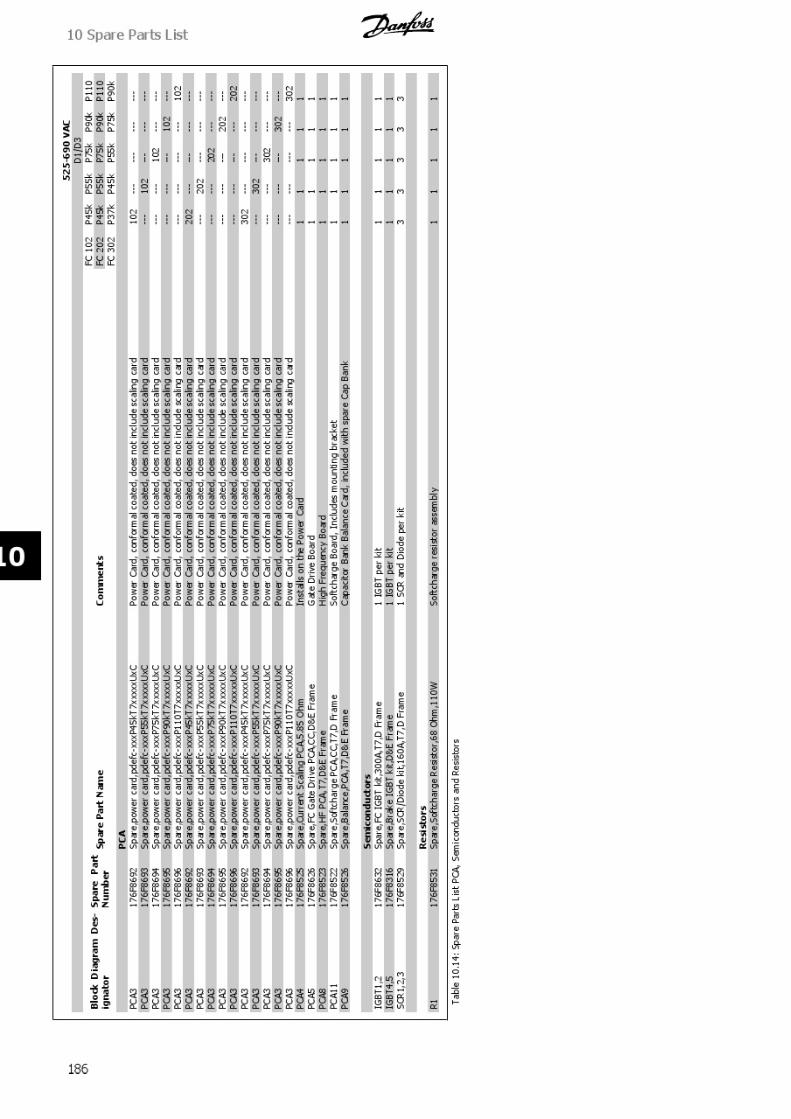
7/16/2019 1. D & E Frame.pdf
http://slidepdf.com/reader/full/1-d-e-framepdf 186/197

7/16/2019 1. D & E Frame.pdf
http://slidepdf.com/reader/full/1-d-e-framepdf 187/197
5 2 5 - 6 9 0 V A C
D 1 / D 3
B l o c k
D i a g r a m
D e s -
i g n a t o
r
S p a r e
P a r t
N u m b e r
S p a r e P a r t N a m e
C o m
m e n t s
F C 1 0 2
P 4 5 k
P 5 5 k
P 7 5 k
P 9 0 k
P 1 1 0
F C 2 0 2
P 4 5 k
P 5 5 k
P 7 5 k
P 9 0 k
P 1 1 0
F C 3 0 2
P 3 7 k
P 4 5 k
P 5 5 k
P 7 5 k
P 9 0 k
C a p a c i t o r s
C 2 , 3 , 4 ,
5 , 6 , 7 , 8 , 9 , 1
0
1 7 6 F 8 5 3 4
S p a r e , C
A P , I G
B T
S n u b b e r , 1 2 5 0 V , 1 u F
I G B T
s n u b b e r c a p s m o u n t e d o n t h e I G B T m o d u l e s
3
3
3
3
3
C B A N K 1 , 2
1 7 6 F 8 5 3 2
S p a r e , C
A P B a n k , D
F r a m e , 4 c a p , T
7
C a p a
c i t o r B a n k ,
i n c l u d e s B a l a n c e C a r d
1
1
1
1
1
F a n s
F 1 + C 1
1 7 6 F 8 3 2 9
S p a r e , H e a t s i n k F a n A s s y , D
F r a m e
H e a t
S i n k F a n .
I n c l u d e s f a n ,
f a n b o x , c a p a c i t o r , g a s k
e t , c a b l e s
1
1
1
1
1
F 2 , 3
1 7 6 F 8 3 3 0
S p a r e , D o o r F a n
K i t , D & E F r a m e
D o o r
F a n K i t . I n c l u d e s f a n , g r i l l s , s u p p o r t , f a s t e n e r s ( 1 f a n p e r k i t )
2 1 / 5 4
2 1 / 5 4
2 1 / 5 4
2 1 / 5 4
2 1 / 5 4
1 7 6 F 8 3 3 1
S p a r e , D o o r V e n t K i t , D % E F r a m e
D o o r
V e n t K i t . I n c l u d e s g r i l l , s u p p o r t , f a s t e n e r s ( 1 v e
n t p e r k i t )
2 1 / 5 4
2 1 / 5 4
2 1 / 5 4
2 1 / 5 4
2 1 / 5 4
1 7 6 F 8 3 3 2
S p a r e , D o o r F a n
F i l t e r , P K G 1 0 , D
& E F r a m e
D o o r
F i l t e r s ,
P a c k a g e o f 1 0
I P 5 4
I P 5 4
I P 5 4
I P 5 4
I P 5 4
F 4
1 7 6 F 8 6 3 9
S p a r e , F
C D C T o p F a n , I P
0 0 D F r a m e
I P 0 0
T o p F a n ,
F a n O n l y ( 1 f a n p e r k i t )
I P 0 0
I P 0 0
I P 0 0
I P 0 0
I P 0 0
F 2 , 3
1 7 6 F 8 3 3 3
S p a r e , D o o r / T o p
A C F a n , D
& E F r a m e
I P 2 1 / I P 5 4 D o o r F a n ,
F a n O n l y ( 1 f a n p e r k i t )
2 1 / 5 4
2 1 / 5 4
2 1 / 5 4
2 1 / 5 4
2 1 / 5 4
F u s e s
F U 1 , 2 , 3
1 7 6 F 8 3 3 4
S p a r e , F u s e , M a i n
, 3 5 0 A
M a i n
s F u s e .
1 f u s e p e r k i t
- - -
- - -
- - -
- - -
3
F U 1 , 2 , 3
1 7 6 F 8 5 3 9
S p a r e , F u s e , M a i n
, 2 0 0 A
M a i n
s F u s e .
1 f u s e p e r k i t
3
3
3
3
- - -
1 7 6 F 8 3 3 6
S p a r e , F u s e , S o f t c h a r g e , 2
0 A , P
K G 3 , D
& E F r a m e
S o f t c
h a r g e f u s e .
P a c k a g e o f 3
1 p k g
1 p k g
1 p k g
1 p k g
1 p k g
F U 5
1 7 6 F 8 4 4 0
S p a r e , F u s e , 4
A , P
K G 3 , P o w e r P C A , F a n
P o w e r C a r d F u s e ,
4 a m p .
P a c k a g e o f 3
1
1
1
1
1
F U 4
1 7 6 F 8 4 4 0
S p a r e , F u s e , 4
A , P
K G 3 , P o w e r P C A , F a n
F a n T r a n s f o r m e r F u s e ,
4 a m p .
P a c k a g e o f 3
1
1
1
1
1
I n d u c t o r s a n d
C u r r e n t S e n s o r s
L 1
1 7 6 F 8 5 3 6
S p a r e , B u s I n d u c
t o r , 3 5 0 u H
D C L
i n k C o i l , S m a l l D F r a m e
1
1
1
1
1
L 2 , 3 , 4
1 7 6 F 8 3 4 2
S p a r e , C u r r e n t S e n s o r , 3 0 0 A
M o t o
r C u r r e n t S e n s o r , 1 s e n s o r p e r k i t
3
3
3
3
3
T R 1
1 7 6 F 8 5 3 5
S p a r e , F a n T r a n s
f o r m e r A s s y , 6
9 0 V , 4
0 0 V A
F a n T r a n s f o r m e r . I n c l u d e s c a b l e s a n d p l u g
1
1
1
1
1
T a b l e
1 0 . 1
5 : S p a r e P a r t s L i s t C a p a c i t o r s ,
F a n s , F u s e s a n d I n d u c t o r s & C u r r e n t S e n s o r s
10 Spare Parts List
187
10

7/16/2019 1. D & E Frame.pdf
http://slidepdf.com/reader/full/1-d-e-framepdf 188/197
5 2 5 - 6 9 0 V A C
D 1 / D 3
B l o c k
D i a g r a m
D e s -
i g n a t o
r
S p a r e
P a r t
N u m b e r
S p a r e P a r t N a m e
C o m
m e n t s
F C 1 0 2
P 4 5 k
P 5 5 k
P 7 5 k
P 9 0 k
P 1 1 0
F C 2 0 2
P 4 5 k
P 5 5 k
P 7 5 k
P 9 0 k
P 1 1 0
F C 3 0 2
P 3 7 k
P 4 5 k
P 5 5 k
P 7 5 k
P 9 0 k
D i s c o n n e c t s
S W 1
1 7 6 F 8 3 4 5
S p a r e , D
i s c o n n e c
t S W , 2
0 0 A , D
F r a m e
D i s c o
n n e c t S w i t c h
1
1
1
1
1
1 7 6 F 8 3 4 6
S p a r e , D
i s c o n n e c
t H a n d l e , R o d , D
F r a m e
D i s c o
n n e c t H a n d l e
1
1
1
1
1
C a b l e s
C B L 1
1 7 6 F 8 6 4 0
S p a r e , C a b l e , F C
L C P , D
F r a m e , I P
5 4
r i b b o
n c a b l e f r o m L C P t o c o n t r o l c a r d ,
I P 5 4 e n c l o s u r e
I P 5 4
I P 5 4
I P 5 4
I P 5 4
I P 5 4
C B L 2
1 7 6 F 8 6 4 1
S p a r e , C a b l e , C o n
t r o l P C A , 4
4 p i n , D
& E F r a m e
r i b b o
n c a b l e f r o m C o n t r o l C a r d t o P o w e r C a r d
1
1
1
1
1
C B L 5
1 7 6 F 8 5 4 1
S p a r e , C a b l e , F C
C u r r e n t S e n s o r , D F r a m e
w i r e
h a r n e s s f r o m p o w e r c a r d t o c u r r e n t s e n s o r s
1
1
1
1
1
C B L 8
1 7 6 F 8 5 4 2
S p a r e , C a b l e , H S
F a n , D
1 F r a m e
w i r e
h a r n e s s f r o m p o w e r c a r d t o f a n t r a n s f o r m e r
1
1
1
1
1
C B L 9
1 7 6 F 8 3 5 4
S p a r e , C a b l e , S o f
t c h g R S T p r i m e , D
F r a m e
w i r e
h a r n e s s f r o m s o f t c h a r g e t o p o w e r c a r d
1
1
1
1
1
C B L 1 2
1 7 6 F 8 3 5 8
S p a r e , C a b l e , D o o
r F a n , D
F r a m e
w i r e
h a r n e s s f o r A C d o o r f a n s
2 1 / 5 4
2 1 / 5 4
2 1 / 5 4
2 1 / 5 4
2 1 / 5 4
C B L 1 3
1 7 6 F 8 5 4 4
S p a r e , C a b l e , F C
S C R , D
1 F r a m e
w i r e
h a r n e s s f r o m p o w e r c a r d t o S C R
1
1
1
1
1
C B L 1 4
1 7 6 F 8 3 5 6
S p a r e , C a b l e , D C
t o P o w e r P C A , D
F r a m e
v o l t a
g e f r o m D C b u s t o p o w e r c a r d
1
1
1
1
1
C B L 1 6
1 7 6 F 8 3 6 3
S p a r e , C a b l e , F C
G a t e D r i v e , 1
6 p i n , D
1 F r a m e
r i b b o
n c a b l e f r o m p o w e r c a r d t o g a t e d r i v e c a r d
1
1
1
1
1
C B L 1 7 , 1 8 , 1
9
1 7 6 F 8 3 6 4
S p a r e , C a b l e , I G B
T G a t e , D
1 F r a m e
w i r e
h a r n e s s f r o m g a t e d r i v e c a r d t o I G B T m o d u l e ( 1
p e r k i t )
3
3
3
3
3
C B L 2 0
1 7 6 F 8 3 5 2
S p a r e , C a b l e , I G B
T T e m p e r a t u r e
t e m p
e r a t u r e c o n e c t i o n f r o m I G B T m o d u l e t o g a t e d r i v e c a r d
1
1
1
1
1
C B L 2 1
1 7 6 F 8 3 6 5
S p a r e , C a b l e , B r a
k e I G B T , D
1 F r a m e
w i r e
h a r n e s s f r o m g a t e d r i v e c a r d t o b r a k e I G B T m o d u l e
1
1
1
1
1
C B L 2 2
1 7 6 F 8 3 6 6
S p a r e , C a b l e , B r a
k e P o w e r P l u s , D 1 F r a m e
c a b l e
f r o m b r a k e I G B T t o b r a k e p l u s t e r m i n a l
1
1
1
1
1
C B L 2 3
1 7 6 F 8 3 6 7
S p a r e , C a b l e , B r a
k e P o w e r M i n u s , D 1 F r a m e
c a b l e
f r o m b r a k e I G B T t o b r a k e m i n u s t e r m i n a l
1
1
1
1
1
C B L 2 4
1 7 6 F 8 5 4 3
S p a r e , C a b l e , S o f
t c h g R S T , D
1 F r a m e
w i r e
h a r n e s s f r o m i n p u t p o w e r t o s o f t c h a r g e b o a r d
1
1
1
1
1
C B L 2 5
1 7 6 F 8 3 5 5
S p a r e , C a b l e , S o f
t c h g t o D C b u s , D F r a m e
w i r e
h a r n e s s f r o m s o f t c h a r g e t o D C b u s
1
1
1
1
1
T a b l e
1 0 . 1
6 : S p a r e P a r t s L i s t D i s c o n n e c t s a n d C a b l e s
10 Spare Parts List
188
10
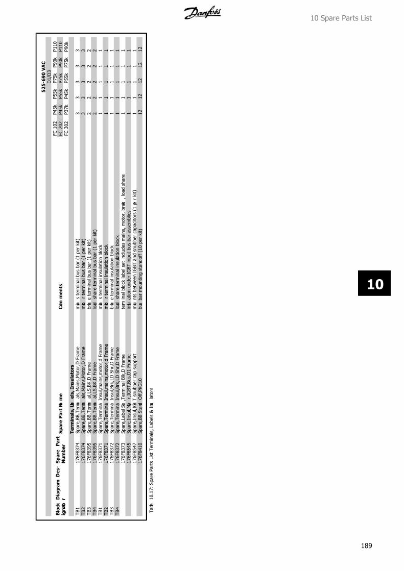
7/16/2019 1. D & E Frame.pdf
http://slidepdf.com/reader/full/1-d-e-framepdf 189/197
5 2 5 - 6 9 0 V A C
D 1 / D 3
B l o c k
D i a g r a m
D e s -
i g n a t o
r
S p a r e
P a r t
N u m b e r
S p a r e P a r t N a m e
C o m
m e n t s
F C 1 0 2
P 4 5 k
P 5 5 k
P 7 5 k
P 9 0 k
P 1 1 0
F C 2 0 2
P 4 5 k
P 5 5 k
P 7 5 k
P 9 0 k
P 1 1 0
F C 3 0 2
P 3 7 k
P 4 5 k
P 5 5 k
P 7 5 k
P 9 0 k
T e r m i n a l s ,
L a b
e l s ,
I n s u l a t o r s
T B 1
1 7 6 F 8 3 7 4
S p a r e , B
B , T e r m i n
a l s , M a i n s , M o t o r , D F r a m e
m a i n
s t e r m i n a l b u s b a r ( 1 p e r k i t )
3
3
3
3
3
T B 2
1 7 6 F 8 3 7 4
S p a r e , B
B , T e r m i n
a l s , M a i n s , M o t o r , D F r a m e
m o t o
r t e r m i n a l b u s b a r ( 1 p e r k i t )
3
3
3
3
3
T B 3
1 7 6 F 8 3 9 5
S p a r e , B
B , T e r m i n
a l , L S , B
K , D
F r a m e
b r a k e t e r m i n a l b u s b a r ( 1 p e r k i t )
2
2
2
2
2
T B 4
1 7 6 F 8 3 9 5
S p a r e , B
B , T e r m i n
a l , L S , B
K , D
F r a m e
l o a d
s h a r e t e r m i n a l b u s b a r ( 1 p e r k i t )
2
2
2
2
2
T B 1
1 7 6 F 8 3 7 1
S p a r e , T e r m i n a l I n s u l , m a i n s , m o t o r , d F r a m e
m a i n
s t e r m i n a l i n s u l a t i o n b l o c k
1
1
1
1
1
T B 2
1 7 6 F 8 3 7 1
S p a r e , T e r m i n a l I n s u l , m a i n s , m o t o r , d F r a m e
m o t o
r t e r m i n a l i n s u l a t i o n b l o c k
1
1
1
1
1
T B 3
1 7 6 F 8 3 7 2
S p a r e , T e r m i n a l I n s u l , B r k , L
D S h r , D F r a m e
b r a k e t e r m i n a l i n s u l a t i o n b l o c k
1
1
1
1
1
T B 4
1 7 6 F 8 3 7 2
S p a r e , T e r m i n a l I n s u l , B r k , L
D S h r , D F r a m e
l o a d
s h a r e t e r m i n a l i n s u l a t i o n b l o c k
1
1
1
1
1
1 7 6 F 8 3 7 3
S p a r e , L a b e l S e t , T e r m i n a l B l k , D
F r a m e
t e r m i n a l b l o c k l a b e l s e t i n c l u d e s m a i n s , m o t o r , b r a k e ,
l o a d s h a r e
1
1
1
1
1
1 7 6 F 8 5 4 5
S p a r e , I n s u l , M y l a
r , I G B T , B u s , D 1 F r a m e
i n s u l a t i o n u n d e r I G B T i n p u t b u s b a r a s s e m b l i e s
1
1
1
1
1
1 7 6 F 8 5 4 7
S p a r e , I n s u l , I G B T s n u b b e r c a p s u p p o r t
m o u n t s b e t w e e n I G B T a n d s n u b b e r c a p a c i t o r s ( 1 p e r k i t )
1
1
1
1
1
1 7 6 F 8 4 1 0
S p a r e , B
B S t a n d
O f f , P K G 1 0
b u s b a r m o u n t i n g s t a n d o f f ( 1 0 p e r k i t )
1 2
1 2
1 2
1 2
1 2
T a b l e
1 0 . 1
7 : S p a r e P a r t s L i s t T e r m i n a l s ,
L a b e l s & I n s u
l a t o r s
10 Spare Parts List
189
10

7/16/2019 1. D & E Frame.pdf
http://slidepdf.com/reader/full/1-d-e-framepdf 190/197
5 2 5 - 6 9 0 V A C
D 1 / D 3
B l o c k D i a g r a m D
e s -
i g n a t o
r
S p a r e
P a r t
N u m b e r
S p a r e P a r t N a m
e
C o m m e n t s
F C 1 0 2
P 4 5 k P
5 5 k
P 7 5 k
P 9 0 k
P 1 1 0
F C 2 0 2
P 4 5 k P
5 5 k
P 7 5 k
P 9 0 k
P 1 1 0
F C 3 0 2
P 3 7 k P
4 5 k
P 5 5 k
P 7 5 k
P 9 0 k
B u s B a r s
1 7 6 F 8 3 8 0
S p a r e , B
B , S
C R , R \ S
\ T , D
F r a m e
c o n n e c t s i n p u t p l a t e b u s b a r t o S C R i n p u t ( 1 p e r k i t )
3
3
3
3
3
1 7 6 F 8 5 4 8
S p a r e , B r k t , S C R B B S u p p o r t , D F r a m e
S C R i n p u t b u s b a r s u p p o r t
1
1
1
1
1
1 7 6 F 8 3 7 9
S p a r e , B
B A s s y , S C
R , D
F r a m e
c o n n e c t s t o S C R o u t p u t s , s a n d w i c h a s s e m b l y
1
1
1
1
1
1 7 6 F 8 3 8 1
S p a r e , B
B , S
C R , M i n
u s , D F r a m e
c o n n e c t s D C c o i l i n p u t s t o S C R o u t p u t b u s b a r a s s e m b l y ( 1 p e r k i t )
2
2
2
2
2
1 7 6 F 8 5 4 9
S p a r e , B
B , D
C L i n k , P
l u s , D F r a m e
c o n n e c t s D C P l u s c o i l o u t p u t t o I G B T i n p u t b u s b a r a s
s e m b l y
1
1
1
1
1
1 7 6 F 8 3 9 1
S p a r e , B
B , D
C L i n k , P
l u s , D F r a m e
c o n n e c t s D C M i n u s c o i l o u t p u t t o I G B T i n p u t b u s b a r
a s s e m b l y
1
1
1
1
1
1 7 6 F 8 3 7 6
S p a r e , B
B A s s y , I G
B T , D
F r a m e
c o n n e c t s c a p a c i t o r b a n k a n d I G B T i n p u t s , s a n d w i c h a
s s e m b l y
1
1
1
1
1
1 7 6 F 8 3 9 0
S p a r e , B
B , I G
B T , U \
V \ W , D
F r a m e
c o n n e c t s I G B T o u t p u t t o l o n g b u s b a r o v e r t h e f a n ( 1
p e r k i t )
3
3
3
3
3
1 7 6 F 8 3 9 2
S p a r e , B
B , M o t o r , 2 , D
F r a m e
l o n g o u t p u t b u s b a r o v e r t h e f a n ( 1 p e r k i t )
3
3
3
3
3
1 7 6 F 8 3 9 7
S p a r e , B
B , B r a k e , P l u s , D F r a m e
c o n n e c t s D C P l u s t o b r a k e I G B T
1
1
1
1
1
1 7 6 F 8 3 9 8
S p a r e , B
B , B r a k e , M
i n u s , D F r a m e
c o n n e c t s D C M i n u s t o b r a k e I G B T
1
1
1
1
1
1 7 6 F 8 4 0 1
S p a r e , B
B , L
S , P
l u s ,
D F r a m e
c o n n e c t s p l u s l o a d s h a r e t e r m i n a l t o S C R o u t p u t b u s b a r a s s e m b l y
1
1
1
1
1
1 7 6 F 8 4 0 0
S p a r e , B
B , L
S , M
i n u
s , D F r a m e
c o n n e c t s m i n u s l o a d s h a r e t e r m i n a l t o S C R o u t p u t b u
s b a r a s s e m b l y
1
1
1
1
1
1 7 6 F 8 4 0 5
S p a r e , B
B , S
C R , I n p
u t 2 , D
F r a m e
l o c a t e d o n i n p u t p l a t e ( 1 p e r k i t )
3
3
3
3
3
1 7 6 F 8 4 0 7
S p a r e , B
B , D
i s c , D F
r a m e
l o c a t e d o n i n p u t p l a t e ( 1 p e r k i t )
3
3
3
3
3
E n c l o s u r e
1 7 6 F 8 4 3 0
S p a r e , C a b l e C l a m
p , 6
0 m m
6 0 m m p o w e r c a b l e c l a m p
- - -
-
- -
- - -
- - -
- - -
1 7 6 F 8 4 9 0
S p a r e , B r k t , H F , b o a r d , g n d , D
F r a m e
m o u n
t i n g b r a c k e t f o r h i g h f r e q u e n c y b o a r d
1
1
1
1
1
T a b l e
1 0 . 1
8 : S p a r e P a r t s L i s t B u s B a r s a n d E n c l o s u r e
10 Spare Parts List
190
10
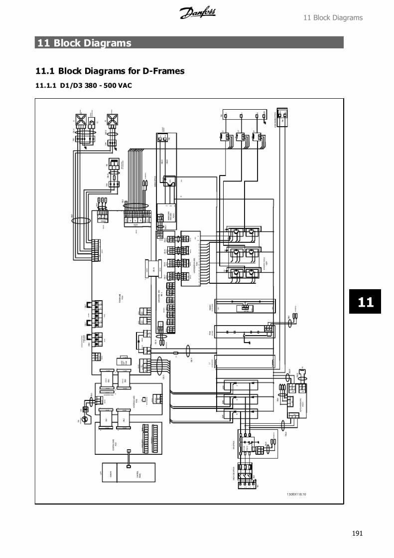
7/16/2019 1. D & E Frame.pdf
http://slidepdf.com/reader/full/1-d-e-framepdf 191/197
11 Block Diagrams
11.1 Block Diagrams for D-Frames
11.1.1 D1/D3 380 - 500 VAC
130BX118.10
D C I N D U C T O R
G N D
L 1 R
M K 1 0 5
R S - 4 8 5
M K 1 0 0
A N A L O G I / O
M K 1 0 1
D I G I T A L I N P U T S
6 0
5 5
5 4
5 3
5 0
4 5
4 2
3 9
1 3
1 2
0 5
0 4
6 9
6 8
6 1
3 3
3 2
2 9
2 7
2 0
1 9
1 8
1 7
1 6
1
M K 1 0 3
2 8 1
2 8
M K 1 0 4
C O N T R O L C A R D
L C P 1
P A N E L
C O N T R O L
D I S P L A Y
S L 2 T L 3
-
M
+ I U I V
+
M
-
G N D
U V W
-
M I W +
M A I N SI W
' I V '
I U '
S E N S O R S
C U R R E N T
T S R
S C R
G A T E D R I V E R
R
S
T
R '
R F I O P T I O N
S
+
-
U N
U P
V N
V P
W N
W P
- + - +
S '
T '
R S T
- S C R
+ S C R
P O W E R C A R D
S O F T C H A R G E B O A R D
D I S C / F U S E O P T I O N
R
S
T
I N T E R F A C E C A R D
N C
N O
C
A
- D C
A U X 1
B
+ D C
+ D C
- D C
C
N O
N C
A U X 2
H E A T S I N K N T C
+ -
H F C A R D
+ -
P 4 0 0 C C
L E G A C Y
T E S T C O N N E C T O R
C
N C
N O
( D I S A B L E M A I N S R E C T I F I E R )
1 0 5
1 0 6
1 0 4
E X T E R N A L B R A K E
T E M P S W I T C H
H F S W
V D D
R L 2
+ -
A U X F A N
E X T 2 4 V
R E L A Y
R E L A Y
F A N S
R '
S '
T '
R '
S ' T
'
-
+
- +
D C C A P B A N K
E C O N O P A C K + M O D U L
E
C U R R E N T
S C A L I N G
C A R D
L 1
L 2
L 1
L 2
C C F A N
M K 1 0 1
M K 1 0 4
M K 1 0 3
M K 1 0 5 M K 1 0 2
M K 1 1 0 M K 1 0 4
M K 1 0 0
F K 1 0 0
-
+
3 5
3 6
1 0 1
A U X
_ T
T 1 0 3
A U X
_ S
1 0 0
S 1 0 2
1
2
3
4
5
6
X 2
X 1
L 1
L 1
A U X _ T
A U X _ S
A U X _ T
A U X _ S
M K 1 0 3
F K 1 0 2
F K 1 0 3
M K 1 0 0
M K 1 0 5
F K 1 0 0
F K 1 0 1
M K 1 0 7
M K 1 0 6
M K 1 0 2
M K 1 1 1
A
- D C C
M K 4 0 0
9 1
9 2
9 3 9
4
9 5
9 8 9
7 9 6 8
9 8 8
F A N O
V D D
U D C +
U D C -
M K 1 0 0
M K 1 C B A
B A L C K T
F K 1
F K 2
F K 3
F K 4
F K 5
F K 6
M K 1
M K 1
M K 2
A C A B
R S +
R S -
M K 3 M K 4
N T C
- +
G A T E R E S I S T O R C A R D
E U P 1
C U P 1
G U P 1
G L O 1
E L O 1
OUT
IN
M K 1 0 3
N T C
M K 1 0 4
M K 6 5 0
M K 4 5 0
M K 2 5 0
M K 3 5 0
P R E T E S T
M K 5 5 0
G A T E D R I V E C
A R D
R F I S W
R L 2
V D D
M K 1 0 1
M K 8 5 0
M K 7 5 0
M K 1 0 3
U M K 1 0 2
M K 1 0 6
M K 1 0 0
M K 1 0 5
M K 1 0 9
E U P 2
G U P 2
C U P 2
G L O 2
E L O 2
E U P 3
G U P 3
C U P 3
G L O 3
E L O 3
H F S W I T C H
R F I S W I T C H
H F S W I T C H
R F I S W I T C H
H S N T C
1 8 P U L S E N T C
F U 1
F U 2
F U 3
1 2
1 2
T M P _ P
T M P _ N
R F I / H F S W I T C H
O N
1 2
P C A 1
T H 1
C B L 1
C B L 2
C B L 3
C B L 4
P C A 2
P C A 3
C N 1
C B L 5
C B L 5
P C A
5
P C A 6
P C A 8
P C A 1 1
L 1
C B A N K 1
S C R 1
S C R 2
S C R 3
I G B T 1
C 2
C 3
C 4
L 2 L 3
L 4
R 1
S W 1
R F I C A R D
B R A K E O P T I O N
U D C -
U D C +
M K 1
B R A K E G A T E
R E S C A R D
G A T E E M C O L
B R A K E I G B T
E X T B R A K E
R +
8 2
8 1
R -
R E S I S T O R
I G B T 3
+ D C
P C A 9
P C A 1 2
P C A 1 3
F 2
D O O R F A N
1
1
3 2
3 2
C N 4
G N D
F A N -
F A N +
F A N C A P A C I T O R
H E A T S I N K
C N 3
5 4 3 1 2
4 5 6
6
2 1 4
C 1
H E A T S I N K
3 2 1
3 2 1
F 1
F A N
1
1
2 3
2 3
C N 2
F U 4
C O M
F A N T R A N S F O R M E R
H E A T S I N K / D O O R
1
T R 1
I N O U T
3 2
C B L 6
C B L 7
C B L 7
C B L 1 3
C B L 1 4
C B L 8
C B L 9
C B L 1 0
C B L 1 1
C B L 1 2
C B L 1 5
C B L 1 6
C B L 1 7
C B L 2 0
C B L 2 1
C B L 2 3
C B L 2 2
C B L 5
C B L 1 5
C B L 2 4
C B L 9
C B L 2 5
C B L 2 6
P C A 4
C B L 1 8
C B L 1 9
L O A D S H A R E O P T I O N
T B 3
T B 1
T B 2
T B 4
S 2 0 1
F U 5
1 2 9
1 2 9
1
2
3
1
1
2 9
2 9
4 3
1
2
4
1
3
3
6
2
5
1
4
1 2 9
4 3 1
2
1
3
T M P
G N D
3
2
1
6
5
4
3
2
1
3
5
4
1 3
1 1 1 2
9
8
1
6
1 0 5 8 3 6 1
G N D
V P O S
S E N S
D E T
I U 1
V N E G
V P O S
I V 1
V N E G
V P O S
I W 1
V N E G
1 0 1
1 1 2 3 4 5 6 7 8 1 6
1 4
1 5
1 2
1 3 9
C U R
1
1 5
3
2
1 2 3
3 2 1
G U P
G U N
E U P
E U N
1
5
6
1 0
E V P
G V N
G V P 1
6
5 V
E V N
1 0
E W P
G W N
G W P 1
6
5 W
E W N
1 0
GLO1
EUP1
ELO1
UGUP1 4
5
8
1
M K 1 0 0
V M K 1 0 0
GUP2 4
EUP2
GLO2
8
5
ELO2 1
W M K 1 0 0
GUP3 4
EUP3
GLO3
8
5
ELO3 1
T M P +
T M P -
N T C
1
2
3
NTC1
NTC2
N T C
1
2
3
E U N
G U N 1
3
2 G U N
G U P E U P
2 G U P
1
3
G V N E V N
2 G V N
1
G V P E V P
G V P
3
1
2
3
G W N E W N
2 G W N
1
G W P E W P
G W P
3
1
2
3
B R K B R N
G B P 2
1
3
G 2
E 1 / C 2
46 1
1 5 6
B R K
B R K
B R C
B R N
G B P
E 2
11 Block Diagrams
191
11

7/16/2019 1. D & E Frame.pdf
http://slidepdf.com/reader/full/1-d-e-framepdf 192/197
11.1.2 D2/D4 380 - 500 VAC
130BX119.10
D C I N D U C T O R
G N D
L 1
R
M K 1 0 5
R S - 4 8 5
M K 1 0 0
A N A L O G I / O
M K 1 0 1
D I G I T A L I N P U T S
6 0
5 5
5 4
5 3
5 0
4 5
4 2
3 9
1 3
1 2
0 5
0 4
6 9
6 8
6 1
3 3
3 2
2 9
2 7
2 0
1 9
1 8
1 7
1 6
C O N T R O L C A R D
L C P 1
P A N E L
C O N T R O L
D I S P L A Y
S L 2
T L 3
-
M
+ I U I V
+
M
-
G N D
U V W
-
M I W
+
F A N
H E A T S I N K
F A N C A P A C I T O R
R '
S
+
-
U N
U P
U N
U P
V N
V P
- + - +
R +
R -
B R A K E I G B T
R S T
- S C R
+ S C R
S O F T C H A R G E B O A R D
H E A T S I N K
+ D C
- D C
H F C A R D
R '
S '
T '
R '
S ' T
'
N T C
H E A T S I N K / D O O R
F A N T R A N S F O R M E R
D C C A P B A
N K
E C O N O P A C K + M O D U L E
1 2
C O M
O U T
3
I N
9 1
9 2
9 3 9
4
9 5
9 8 9
7 9 6 8
9 8 8
8 1
8 2
U D C +
U D C -
U D C -
U D C +
E X T B R A K E
1 2 3 4 1 2
1 2 3 4 5 6
1 2 3
1 2 3
1 2 3 4 5 6
D O O R F A N
3 2
3 2 1
1
F A N +
F A N -
G N D
M K 1 C B A
B A L C K T
M K 1
M K 2
A C A B
R S +
R S -
M K 3 M K 4
V N
W N
V P
W P
W N
W P
U D C -
- +
B A L C K T
B C M K 1
A
+ -
U D C +
D C C A P B A N K
N T C
E C O N O P A C K + M O D U L E
R E S I S T O R
B R A K E O P T I O N
B R A K E I G B T
P C A 1
C B L 5
2
2 1
1
H E A T S I N K N T C
T H 1
C N 1
C N 2
T R 1
C N 3
F 1
C N 4
F 2
C 1
F U 3
D I S C / F U S E O P T I O N F
U 2
F U 1
F K 3
F K 6
R F I O P T I O N
R F I C A R D
F K 2
F K 1
F K 5
F K 4
S W 1
R
S
T
S C R
1
S C R 2
S C R 3
P C A 8
L 1
C B A N K 1 L O
W E R
C B A N K 2 U P P E R
R 1
I G B T 1
I G B T 2
C 2
C 3
C 4
C 5
C 6
C 7
L 2
L 3 L 4
I G B T 3
I G B T 4
P C A 1 1
P C A 1 2
P C A 9
P C A 1 0
F U 4
C B L 8
C B L 1 1
C B L 1 0
C B L 1 2 C
B L 2 3
C B L 2 2
C B L 2 1
C B L 1 3
C B L 1 4
C B L 2 4
C B L 9
C B L 2 5
C B L 2 6
L O A D S H A R E O P T I O N
T B 3
T B 1
T B 2
T B 4
F U 5
P C A 3
G A T E D R I V E C A R D
P O W E R C A R D
M K 1 0 4 M K 1 0 3
1 2 8
1 2 8
F K 1 0 3
F K 1 0 2
M K 1 0 0
M K 1 0 2
M K 1 0 4
M K 1 0 1
T E S T C O N N E C T O R
4
P C A 4
S C A L I N G
C U R R E N T
T
S
R
4
2 3 5 -
3
1 3 6 +
R F I / H F S W I T C H
F K 1 0 0
E X T 2 4 V
6
3
5
2
1
I N T E R F A C E C A R D
M K 1 0 3 1
S 2 0 1
P C A 2
O N
1 2
2 9
C B L 2
C B L 1
1
2 9
C B L 4
M K 1 1 0
M K 1 0 5 1
G A T E D R I V E R
S C R
M K 1 0 0
1
2 9
4 3
P 4 0 0 C C
C B L 3
L E G A C Y
2 9
4 3
C A R D
M K 1 0 4
+ D C
N C
N O
C
+ D C
C
N O
N C
G U N M
K 1 0 1
V D D
R L 2
M K 2 5 0
R F I S W I T C H
G U N
E U N 2
1
A
B
- +
123
C B L 1 5
A
C
M K 5 5 0
M K 3 5 0
M K 4 5 0
M K 6 5 0
G U P
G U P
E U P
3
1
2
G V N
E V N
3
1
2 G V N
3
G V P
E V P
1
3
2 G V P
G W N
E W N
1
3
2 G W N
R F I S W
2 1
3
4
P R E T E S T
6
5
M K 1 1 1
M K 1 0 5
- D C
M K 4 0 0
- D C
F K 1 0 1
R E L A Y
A U X 2
F K 1 0 0 R
E L A
Y
A U X
1
2 9
H S N T C T M P _ N
T M P _ P
2
1
3
1
1
1
3 1 0 5
N O
1 8 P U L S E N T C
M K 1 0 3 G N D
T M P
2
1
3
1 0 4 C
1 0 6
N C
2
1
1 0
0
A U X
_ S
1 0 2 S 6
5
4
1 0 3 T
A U X
_ T
1 0 1
3
2
1
H F S W I T C H
M A I N S
G B P
G B P
B R N
C B L 1 6
M K 1 0 2
M K 7 5 0
M K 8 5 0
G W P
E W P
1
3
2 G W P
G B P
B R N 2
1
3
B R K
G U N
G U P
G U P 1
6
2
U G U N 7
P C A 5
C B L 1 7
M K 1 0 6
M K 1 0 9
M K 1 0 0
M K 1 0 3
M K 1 0 4
T M P -
T M P + 2
1
3
N T C
C B L 1 9
C B L 1 8
M K 1 0 5 C B L 2 0
1 5
1
C C F A N
1 2 6
G N D
V D D
F A N O
9 1 3
1 2
-
1 0
S E N S
C U R
H F S W
I U '
I W '
M K 1 0 2
C U R R E N T
S E N S O R S
I V '
5
V N E G
R L 2
V D D
1 5 1 4
1 6
I W 1
V P O S
V N E G
8 7 6 2
I U 1
V P O S
V N E G
I V 1
4 3
D E T
V P O S
1 1 1
T
1 6
+
C B L 5 T
'
M K 1 0 7
L 2
L 1
F A N S
L 1
L 1
L 2
5
3
1 3
4
1 1
X 2
A U X _ S
L 1
A U X _ S
A U X _ T
X 1
A U X _ T
9
1 2
1
8
6
C B L 9
M K 1
0 6
R S
3 8 5 1 0
S '
C B L 6
T E M P S W I T C H
( D I S A B L E M A I N S R E C T I F I E R )
E X T E R N A L B R A K E
A U X F A N
C B L 7
C B L 7
M K 1 0 0 -
1
+
3 2
- +
H F S W I T C H
C B L 5
+
-
M K 1
3
2
- +
R F I S W I T C H
C B L 1 5
N T C
V
U
U
G U P 2
G A T E R E S I S T O R C A R D
G U P 1
C U P 1
E U P 1
G L O 1
C U P 2
E L O 1
M K 1 0 0
M K 1 0 0
E U P 3
E L O 2
G L O 2
E U P 2
C U P 3
G U P 3
P C A 6
M K 1 0 0
IN
OUT
G L O 3
E L O 3
N T C
M K 1 0 3
4GUP2
4 GUP1
8
5
EUP1
GLO1
1 ELO1
8EUP2
5GLO2
1 ELO2
5GLO3
4GUP3
1ELO3
8EUP3
3
2
1 NTC1
NTC2
N T C
W
W
V
G U P 2
G A T E R E S I S T O R C A R D
G U P 1
C U P 1
E U P 1
G L O 1
C U P 2
E
L O 1
M K 1 0 0
M K 1 0 0
E U P 3
E L O 2
G L O 2
E U P 2
C U P 3
G U P 3
P C A 7
M K 1 0 0
IN
OUT
G L O 3
E L O 3
N T C
M K 1 0 3
4 GUP2
4GUP1
8
5
EUP1
GLO1
1 ELO1
8EUP2
5GLO2
1ELO2
5GLO3
4 GUP3
1 ELO3
8EUP3
3
2
1 NTC1
NTC2
E U P
E U P
4
5
E U N
E U N
9 1 0
7 G U N
G U N
G U P
G U P 1
2
6
E U N
E U N
E U P
E U P 4
5
9 1 0
U
7 G U N
G U N
G U P
G U P 1
2
6
E U N
E U N
E U P
E U P 4
5
9 1 0
U
C O L
B R A K E G A T E
R E S C A R D
P C A 1 4
E M G A T E
M K 1
B R K
G 2
1
E 2
46
E 1 / C 2
B R A K E G A T E
P C A 1 3
R E S C A R D
E M G A T E
B R K
4
E 2
G 2
1
M K 1
E 1 / C 2
6
C O L
B R K
5
B R C
7
B R N
1 0
B R C
11 Block Diagrams
192
11
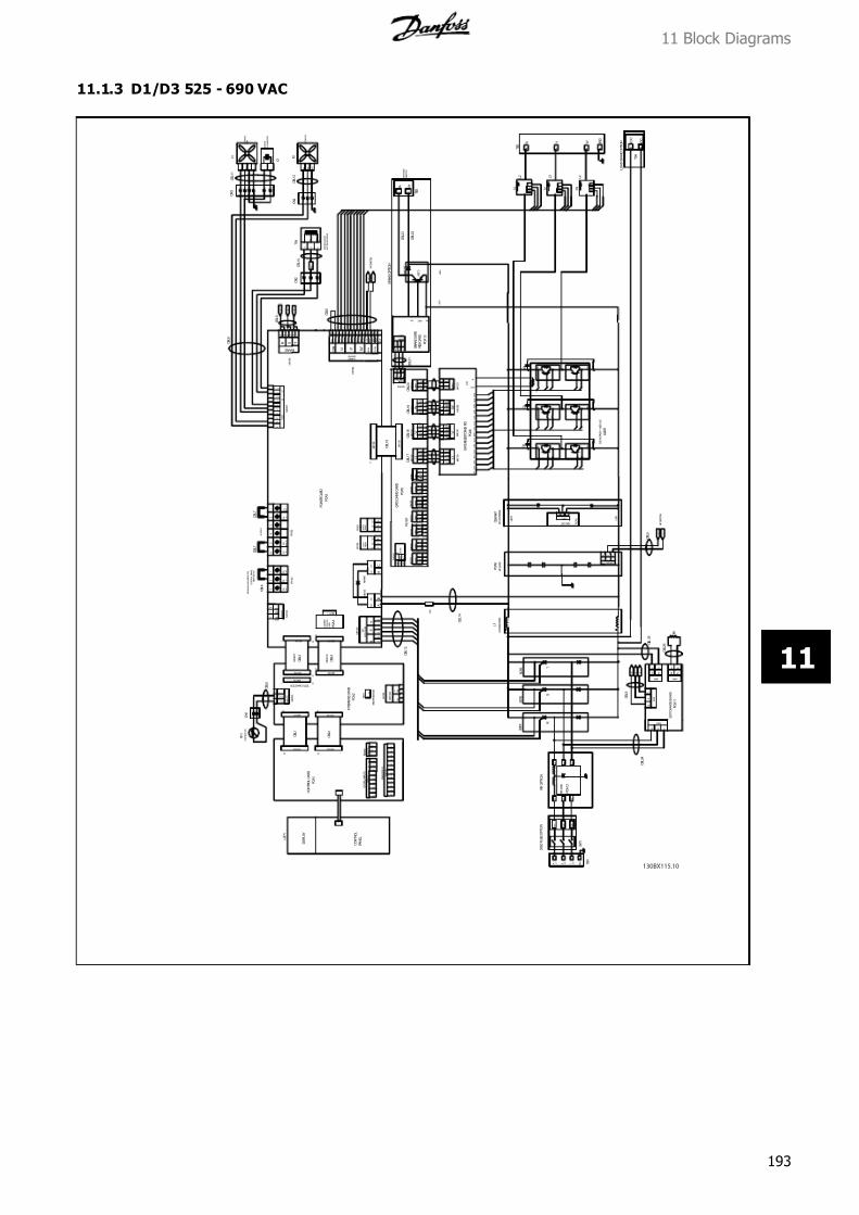
7/16/2019 1. D & E Frame.pdf
http://slidepdf.com/reader/full/1-d-e-framepdf 193/197
11.1.3 D1/D3 525 - 690 VAC
130BX115.10
D C I N D U C T O R
G N D
L 1 R
M K 1 0 5
R S - 4 8
5
M K 1 0 0
A N A L O G I / O
M K 1 0 1
D I G I T A L I N P U T S
6 0
5 5
5 4
5 3
5 0
4 5
4 2
3 9
1 3
1 2
0 5
0 4
6 9
6 8
6 1
3 3
3 2
2 9
2 7
2 0
1 9
1 8
1 7
1 6
1
M K 1 0 3
2 8 1
2 8
M K 1 0 4
C O N T R O L C A R D
L C P 1
P A N E L
C O N T R O L
D I S P L A Y
S L 2 T L 3
-
M
+ I U I V
+
M
-
G N D
U V W
-
M I W +
M A I N SI W
' I V '
I U '
S E N S O R S
C U R R E N T
T S R
S C R
G A T E D R I V E R
R
S
T
R '
R F I O P T I O N
S
+
-
U N
U P
V N
V P
W N
W P
- + - +
S ' T '
R S T
- S C R
+ S C R
P O W E R C A R D
S O F T C H A R G E B O A R D
D I S C / F U S E O P T I O N
R
S
T
I N T E R F A C E C A R D
N C
N O
C
A
- D C
A U X 1
B
+ D C
+ D C
- D C
C
N O
N C
A U X 2
H E A T S I N K N T C
+ -
H F C A R D
+ -
P 4 0 0 C C
L E G A C Y
T E S T C O N N E C T O R
C
N C
N O
( D I S A B L E M A I N S R E C T I F I E R )
1 0 5
1 0 6
1 0 4
E X T E R N A L B R A K E
T E M P S W I T C H
H F S W
V D D
R L 2
+ -
A U X F A N
E X T 2 4 V
R E L A Y
R E L A Y
F A N S
R '
S '
T '
R '
S ' T '
D C C A P B A N K
E C O N O P A C K + M O D U L E
C U R R E N T
S C A L I N G
C A R D
L 1
L 2
L 1
L 2
C C F A N
M K 1 0 1
M K 1 0 4
M K 1 0 3
M K 1 0 5 M K 1 0 2
M K 1 1 0 M K 1 0 4
M K 1 0 0
F K 1 0 0
-
+
3 5
3 6
1 0 1
A U X
_ T
T 1 0 3
A U X
_ S
1 0 0
S 1 0 2
1
2
3
4
5
6
X 2
X 1
L 1
L 1
A U X _ T
A U X _ S
A U X _ T
A U X _ S
M K 1 0 3
F K 1 0 2
F K 1 0 3
M K 1 0 0
M K 1 0 5
F K 1 0 0
F K 1 0 1
M K 1 0 7
M K 1 0 6
M K 1 0 2
M K 1 1 1
A
- D C C
M K 4 0 0
9 1
9 2 9 3 9 4
9 5 9 8 9 7
9 6 8 9
8 8
F A N O
V D D
U D C +
U D C -
M K 1 0 0
M K 1 C B A
B A L C K T
F K 1
F K 2
F K 3
F K 4
F K 5
F K 6
M K 1
M K 2
A C A B
R S +
R S -
M K 3 M K 4
N T C
G A T E R E S I S T O R C A R D
E U P 1
C U P 1
G U P 1
G L O 1
E L O 1
OUT
IN
M K 1 0 3
N T C
M K 1 0 4
M K 6 5 0
M K 4 5 0
M K 2 5 0
M K 3 5 0
P R E T E S T
M K 5 5 0
G A T E D R I V E C A R D
R F I S W
R L 2
V D D
M K 1 0 1
M K 8 5 0
M K 7 5 0
M K 1 0 3
U M K 1 0 2
M K 1 0 6
M K 1 0 0
M K 1 0 5
M K 1 0 9
E U P 2
G U P 2
C U P 2
G L O 2
E L O 2
E U P 3
G U P 3
C U P 3
G L O 3
E L O 3
H F S W I T C H
H F S W I T C H
H S N T C
1 8 P U L S E N T C
F U 1
F U 2
F U 3
1 2
1 2
T M P _ P
T M P _ N
R F I / H F S W I T C H
O N
1 2
P C A 1
T H 1
C B L 1
C B L 2
C B L 3
C B L 4
P C A 2
P C A 3
C N 1
C B L 5
C B L 5
P C A 5
P C A 6
P C A 8
P C A 1 1
L 1
C B A N K 1
S C R 1
S C R 2
S C R 3
I G B T 1
C 2
C 3
C 4
L 2 L 3 L 4
R 1
S W 1
R F I C A R D
B R A K E O P T I O N
U D C -
U D C +
M K 1
B R A K E G A T E
R E S C A R D
G A T E E M C O L
B R A K E I G B T
E X T B R A K E
R +
8 2
8 1
R -
R E S I S T O R
I G B T 3
+ D C
P C A 9
P C A 1 2
P C A 1 3
F 2
D O O R F A N
1
1
3 2
3 2
C N 4
G N D
F A N -
F A N +
F A N C A P A C I T O R
H E A T S I N K
C N 3
5 4 3 1 2
4 5 6
6
2 1 4
C 1
H E A T S I N K
3 2 1
3 2 1
F 1
F A N
1
1
2 3
2 3
C N 2
F U 4
C O M
F A N T R A N S F O R M E R
H E A T S I N K / D O O R
1
T R 1
I N O U T
3 2
C B L 6
C B L 7
C B L 7
C B L 1 3
C B L 1 4
C B L 8
C B L 9
C B L 1 0
C B L 1 1
C B L 1 2
C B L 1 6
C B L 1 7
C B L 2 0
C B L 2 1
C B L 2 3
C B L 2 2
C B L 5
C B L 2 4
C B L 9
C B L 2 5
C B L 2 6
P C A 4
C B L 1 8
C B L 1 9
L O A D S H A R E O P T I O N
T B 3
T B 1
T B 2
T B 4
S 2 0 1
F U 5
1 2 9
1 2 9
1
2
3
1
1
2 9
2 9
4 3
1
2
4
1
3
3
6
2
5
1
4
1 2 9
4 3
1
2
1
3
T M P
G N D
3
2
1
6
5
4
3
2
1
3
5
4
1 3 1 1 1 2
9
8
1
6
1 0 5 8 3 6 1
G N D
V P O S
S E N S
D E T
I U 1
V N E G
V P O S
I V 1
V N E G
V P O S
I W 1
V N E G
1 0 1 1 1 2 3 4 5 6 7 8 1 6
1 4 1 5 1 2 1
3 9
C U R
1
1 5
1 2 3
3 2 1
G U P
G U N
E U P
E U N
1
5
6 1 0
E V P
G V N
G V P 1
6
5 V
E V N
1 0
E W P
G W N
G W P 1
6
5 W
E W N
1 0
GLO1
EUP1
ELO1
U
GUP1 4
5
8
1
M K 1 0 0
V M K 1 0 0
GUP2 4
EUP2
GLO2
8
5
ELO2 1
W M K 1 0 0
GUP3 4
EUP3
GLO3
8
5
ELO3 1
T M P +
T M P -
N T C
1
2
3
NTC1
NTC2
N T C
1
2
3
E U N
G U N 1
3
2 G U N
G U P E U P
2 G U P
1
3
G V N E V N
2 G V N
1
G V P E V P
G V P
3
1
2
3
G W N E W N
2 G W N
1
G W P E W P
G W P
3
1
2
3
B R K B R N
G B P 2
1
3
G 2
E 1 / C 2
46 1
1 5 6
B R K
B R K
B R C
B R N
G B P
E 2
11 Block Diagrams
193
11

7/16/2019 1. D & E Frame.pdf
http://slidepdf.com/reader/full/1-d-e-framepdf 194/197
11.1.4 D2/D4 525 - 690 VAC
130BX116.10
D C I N D U C T O R
G N D
L 1
R
M K 1 0 5
R S - 4 8 5
M K 1 0 0
A N A L O G I / O
M K 1 0 1
D I G I T A L I N P U T S
6
0
5 5
5 4
5 3
5 0
4 5
4 2
3 9
1 3
1 2
0 5
0 4
6 9
6 8
6 1
3 3
3 2
2 9
2 7
2 0
1 9
1 8
1 7
1 6
C O N T R O L C A R D
L C P 1
P A N E L
C O N T R O L
D I S P L A Y
S L 2
T L 3
-
M
+ I U I V
+
M
-
G N D
U V W
-
M I W
+
F A N
H E A T S I N K
F A N C A P A C I T O R
R '
S
+
-
U N
U P
U N
U P
V N
V P
- + - +
R +
R -
B R A K E I G B T
R S T
- S C R
+ S C R
S O F T C H A R G E B O A R D
H E A T S I N K
+ D C
- D C
H F C A R D
R '
S '
T '
R '
S ' T
'
N T C
H E A T S I N K / D O O R
F A N T R A N S F O R M E R
D C C A P B A N K
E C O N O P A C K + M O D U L E
1 2
C O M
O U T
3
I N
9 1
9 2
9 3 9
4
9 5
9 8 9
7 9 6 8
9 8 8
8 1
8 2
U D C +
U D C -
U D C -
U D C +
E X T B R A K E
1 2 3 4 1 2
1 2 3 4 5 6
1 2 3
1 2 3
1 2 3 4 5 6
D O O R F A N
3 2
3 2 1
1
F A N +
F A N -
G N D
M K 1 C B A
B A L C K T
M K 1
M K 2
A C A B
R S +
R S -
M K 3 M K 4
V N
W N
V P
W P
W N
W P
U D C -
- +
B A L C K T
B C M K 1
A
+ -
U D C +
D C C A P B A N K
N T C
E C O N O P A C K + M O D U L E
R E S I S T O R
B R A K E O P T I O N
B R A K E I G B T
P C A 1
C B L 5
2
2 1
1
H E A T S I N K N T C
T H 1
C N 1
C N 2
T R 1
C N 3
F 1
C N
4
F 2
C 1
F U 3
D I S C / F U S E O P T I O N F
U 2
F U 1
F K 3
F K 6
R F I O P T I O N
R F I C A R D
F K 2
F K 1
F K 5
F K 4
S W 1
R
S
T
S C R 1
S C R 2
S C R 3
P C A 8
L 1
C B A N K 1 L O W E R
C B A N K 2 U P P E R
R 1
I G B T 1
I G B T 2
C 2
C 3
C 4
C 5
C 6
C 7
L 2 L 3 L 4
I G B T 3
I G B T 4
P C A 1 1
P C A 1 2
P C A 9
P C A 1 0
F U 4
C B L 8
C B L 1 1
C B L 1 0
C B L 1 2 C
B L 2 3
C B L 2 2
C B L 2 1
C B L 1 3
C B L 1 4
C B L 2 4
C B L 9
C B L 2 5
C B L 2 6
L O A D S H A R E O P T I O N
T B 3
T B 1
T B 2
T B 4
F U 5
P C A 3
G A T E D R I V E C A R D
P O W E R C A R D
M K 1 0 4 M K 1 0 3
1 2 8 1
2 8
F K 1 0 3
F K 1 0 2
M K 1 0 0
M K 1 0 2
M K 1 0 4
M K 1 0 1
T E S T C O N N E C T O R
4
P C A 4
S C A L I N G
C U R R E N T
T
S
R
4
2 3 5 -
3
1 3 6 +
R F I / H F S W I T C H
F K 1 0 0
E X T 2 4 V
6
3
5
2
1
I N T E R F A C E C A R D
M K 1 0 3 1
S 2 0 1
P C A 2
O N
1 2
2 9
C B L 2
C B L 1
1
2 9
C B L 4
M K 1 1 0
M K 1 0 5 1
G A T E D R I V E R
S C R
M K 1 0 0
1
2 9
4 3
P 4 0 0 C C
C B L 3
L E G A C Y
2 9
4 3
C A R D
M K 1 0 4
+ D C
N C
N O
C
+ D C
C
N O
N C
G U N M
K 1 0 1
V D D
R L 2
M K 2 5 0
G U N
E U N 2
1
A
B
123
A
C
M K 5 5 0
M K 3 5 0
M K 4 5 0
M K 6 5 0
G U P
G U P
E U P
3
1
2
G V N
E V N
3
1
2 G V N
3
G V P
E V P
1
3
2 G V P
G W N
E W N
1
3
2 G W N
R F I S W
2
1
3
4
P R E T E S T
6
5
M K 1 1 1
M K 1 0 5
- D C
M K 4 0 0
- D C
F K 1 0 1
R E L A Y
A U X 2
F K 1 0 0
R E L A Y
A U X 1
2 9
H S N T C T M P _ N
T M P _ P
2
1
3
1
1
1
3 1 0 5
N O
1 8 P U L S E N T C
M K 1 0 3 G N D
T M P
2
1
3
1 0 4 C
1 0 6
N C
2
1
1 0 0
A U X
_ S
1 0 2 S 6
5
4
1 0 3 T
A U X
_ T
1 0 1
3
2
1
H F S W I T C H
M A I N S
G B P
G B P
B R N
C B L 1 6
M K 1 0 2
M K 7 5 0
M K 8 5 0
G W P
E W P
1
3
2 G W P
G B P
B R N 2
1
3
B R K
G U N
G U P
G U P 1
6
2
U G U N 7
P C A 5
C B L 1 7
M K 1 0 6
M K 1 0 9
M K 1 0 0
M K 1 0 3
M K 1 0 4
T M P -
T M P + 2
1
3
N T C
C B L 1 9
C B L 1 8
M K 1 0 5 C B L 2 0
1 5
1
C C F A N
1 2 6
G N D
V D D
F A N O
9 1 3
1 2
-
1 0
S E N S
C U R
H F S W
I U '
I W '
M K 1 0 2
C U R R E N T
S E N S O R S
I V '
5
V N E G
R L 2
V D D
1 5
1 4
1 6
I W 1
V P O S
V N E G
8 7 6 2
I U 1
V P O S
V N E G
I V 1
4 3
D E T
V P O S
1 1 1
T
1 6
+
C B L 5 T
'
M K 1 0 7
L 2
L 1
F A N S
L 1
L 1
L 2
5
3
1 3
4
1 1
X 2
A U X _ S
L 1
A U X _ S
A U X _ T
X 1
A U X _ T
9
1 2
1
8
6
C B L 9
M K 1 0 6
R S
3 8 5 1 0
S '
C B L 6
T E M P S W I T C H
( D I S A B L E M A I N S R E C T I F I E R )
E X T E R N A L B R A K E
A U X F A N
C B L 7
C B L 7
N T C
V
U
U
G U P 2
G A T E R E S I S T O R C A R D
G U P 1
C U P 1
E U P 1
G L O 1
C U P 2
E L O 1
M K 1 0 0
M K 1 0 0
E U P 3
E L O 2
G L O 2
E U P 2
C U P 3
G U P 3
P C A 6
M K 1 0 0
IN
OUT
G L O 3
E L O 3
N T C
M K 1 0 3
4GUP2
4 GUP1
8
5
EUP1
GLO1
1 ELO1
8EUP2
5GLO2
1 ELO2
5GLO3
4GUP3
1ELO3
8EUP3
3
2
1 NTC1
NTC2
N T C
W
W
V
G U P 2
G A T E R E S I S T O R C A R D
G U P 1
C U P 1
E U P 1
G L O 1
C U P 2
E L O 1
M K 1 0 0
M K 1 0 0
E U P 3
E L O 2
G L O 2
E U P 2
C U P 3
G U P 3
P C A 7
M K 1 0 0
IN
OUT
G L O 3
E L O 3
N T C
M K 1 0 3
4 GUP2
4GUP1
8
5
EUP1
GLO1
1 ELO1
8EUP2
5GLO2
1ELO2
5GLO3
4 GUP3
1 ELO3
8EUP3
3
2
1 NTC1
NTC2
E U P
E U P
4
5
E U N
E U N
9 1 0
7 G U N
G U N
G U P
G U P 1
2
6
E U N
E U N
E U P
E U P 4
5
9 1 0
U
7 G U N
G U N
G U P
G U P 1
2
6
E U N
E U N
E U P
E U P 4
5
9 1 0
U
C O L
B R A K E G A T E
R E S C A R D
P C A 1 4
E M G A T E
M K 1
B R K
G 2
1
E 2
46
E 1 / C 2
B R A K E G A T E
P C A 1 3
R E S C A R D
E M G A T E
B R K
4
E 2
G 2
1
M K 1
E 1 / C 2
6
C O L
B R K
5
B R C
7
B R N
1 0
B R C
M K 1 0 0 -
1
+
3 2
- +
H F S W I T C H
C B L 5
11 Block Diagrams
194
11

7/16/2019 1. D & E Frame.pdf
http://slidepdf.com/reader/full/1-d-e-framepdf 195/197

7/16/2019 1. D & E Frame.pdf
http://slidepdf.com/reader/full/1-d-e-framepdf 196/197

7/16/2019 1. D & E Frame.pdf
http://slidepdf.com/reader/full/1-d-e-framepdf 197/197
Index
A Alarm Messages 59
Ama 30
BBrake Control 63
CCoasting 30
Communication Option 64
DDc Link 62
GGraphical Display 25
HHow To Operate The Graphic Local Control Panel (lcp) 25
Index