1. photodetectors for silicon photonic integrated...
TRANSCRIPT
1Photodetectors for silicon
photonic integrated circuitsMolly Piels and John E. Bowers
Department of Electrical and Computer Engineering, University of California Santa
Barbara, Santa Barbara, CA, USA
1.1 Introduction
Silicon-based photonic components are especially attractive for realizing low-cost pho-
tonic integrated circuits (PICs) using high-volume manufacturing processes (Heck
et al., 2013). Due to its transparency in the telecommunications wavelength bands near
1310 and 1550 nm, silicon is an excellent material for realizing low-loss passive opti-
cal components. For the same reason, it is not a strong candidate for sources and detec-
tors, and photodetector fabrication requires the integration of either III/V materials or
germanium if high speed and high efficiency are required. Photodetectors used in pho-
nic integrated circuits, like photodetectors used in most other applications, typically
require large bandwidth, high efficiency, and low dark current. In addition, the devices
must be waveguide-integrated (rather than surface-illuminated) and the process used to
fabricate the photodiode must be compatible with the processes used to fabricate other
components on the chip. For many applications where PICs are a promising solution,
for example microwave frequency generation, coherent receivers, and optical intercon-
nects relying on receiverless circuit designs (Assefa et al., 2010b), the maximum out-
put power is also an important figure of merit.
There are numerous design trade-offs between speed, efficiency, and output
power. Designing for high bandwidth favors small devices for low capacitance.
Small devices require abrupt absorption profiles for good efficiency, but design for
high output power favors large devices with dilute absorption. Most of the work on
silicon-based photodiodes to date has focused on PIN diodes. Both ultra-compact
devices with abrupt absorption profiles and devices with larger active areas have
been demonstrated. The results have been consistent with this trade-off: ultra-
compact devices have shown the highest bandwidth-efficiency products (up to
38 GHz (Virot et al., 2013)), while devices utilizing dilute absorption profiles had
better power handling (up to 19 dBm output power at 1 GHz (Piels et al., 2013)).
Recently, photodetectors with decoupled structures, the separate absorption charge
and multiplication (SACM) avalanche structure and the uni-traveling carrier (UTC)
structure, have been used in both germanium (Piels and Bowers, 2014; Dai et al.,
2010, 2014; Duan et al., 2013) and hybrid III/V-silicon (Beling et al., 2013b) to
push performance past the limits imposed by the PIN structure.
Photodetectors.
© 2016 Elsevier Ltd. All rights reserved.
In this chapter, we will review the status of heterogeneous integration of silicon
waveguides and photodetectors. First, we will cover available fabrication technolo-
gies (both Ge and hybrid III/V-silicon). We will then discuss the design constraints
that are common to all waveguide photodiodes on silicon substrates. We will pres-
ent an overview of demonstrated devices, and lastly conclude and show an outlook
for the future.
1.2 Technology
Waveguide photodiodes on silicon broadly fall into one of two categories:
germanium-based and hybrid III/V-silicon. A number of groups have demonstrated
Ge-based photodiodes in mature fabrication technology based on a CMOS pilot line
(Assefa et al., 2010a; Marris-Morini et al., 2014; Galland et al., 2013). In these
works, the photodiodes have been cofabricated with passive optics, modulators, and
in some cases transistors, but not optical sources (lasers or LEDs). On the other
hand, hybrid or InGaAs-based photodiodes have generally been fabricated using
technology that is further from mass-production capabilities, but that has a full
library of components (competitive with InP substrate-based devices) available
(Koch et al., 2013).
1.2.1 Germanium
Germanium is an appealing absorbing material for use in silicon-based PICs
because it can be integrated into a CMOS pilot line relatively easily (Si/Ge alloyed
contacts are already used in CMOS electronics) and because the bulk material is
absorbing in the entire 1310 nm window and much of the C and L bands. There are
a number of ways to integrate germanium and silicon, but selective area growth by
chemical vapor deposition is the most common for waveguide photodiodes (Michel
et al., 2010). The Si/Ge interface is conductive, and for vertical diodes, one contact
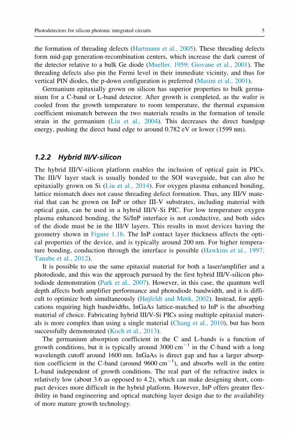
is often composed of silicon. A typical geometry is shown in Figure 1.1a. There is
a 4% lattice mismatch between germanium and silicon, which is relieved through
Substrate
Buried oxideSi rib WG
Substrate
Buried oxideSi rib WG
InPInGaAs absorber
Ge Absorber Side contact
Top contactTop contactSi/Ge waveguide PD
Hybrid III/V-silicon waveguide PD
Side contact
(a) (b)
Figure 1.1 Cross-section schematics of waveguide photodiodes on (a) Si/Ge and (b) hybrid
III/V-silicon. A vertical diode configuration is shown here, but the diode can also be formed
laterally.
4 Photodetectors
the formation of threading defects (Hartmann et al., 2005). These threading defects
form mid-gap generation-recombination centers, which increase the dark current of
the detector relative to a bulk Ge diode (Mueller, 1959; Giovane et al., 2001). The
threading defects also pin the Fermi level in their immediate vicinity, and thus for
vertical PIN diodes, the p-down configuration is preferred (Masini et al., 2001).
Germanium epitaxially grown on silicon has superior properties to bulk germa-
nium for a C-band or L-band detector. After growth is completed, as the wafer is
cooled from the growth temperature to room temperature, the thermal expansion
coefficient mismatch between the two materials results in the formation of tensile
strain in the germanium (Liu et al., 2004). This decreases the direct bandgap
energy, pushing the direct band edge to around 0.782 eV or lower (1599 nm).
1.2.2 Hybrid III/V-silicon
The hybrid III/V-silicon platform enables the inclusion of optical gain in PICs.
The III/V layer stack is usually bonded to the SOI waveguide, but can also be
epitaxially grown on Si (Liu et al., 2014). For oxygen plasma enhanced bonding,
lattice mismatch does not cause threading defect formation. Thus, any III/V mate-
rial that can be grown on InP or other III-V substrates, including material with
optical gain, can be used in a hybrid III/V-Si PIC. For low temperature oxygen
plasma enhanced bonding, the Si/InP interface is not conductive, and both sides
of the diode must be in the III/V layers. This results in most devices having the
geometry shown in Figure 1.1b. The InP contact layer thickness affects the opti-
cal properties of the device, and is typically around 200 nm. For higher tempera-
ture bonding, conduction through the interface is possible (Hawkins et al., 1997;
Tanabe et al., 2012).
It is possible to use the same epitaxial material for both a laser/amplifier and a
photodiode, and this was the approach pursued by the first hybrid III/V-silicon pho-
todiode demonstration (Park et al., 2007). However, in this case, the quantum well
depth affects both amplifier performance and photodiode bandwidth, and it is diffi-
cult to optimize both simultaneously (Højfeldt and Mørk, 2002). Instead, for appli-
cations requiring high bandwidths, InGaAs lattice-matched to InP is the absorbing
material of choice. Fabricating hybrid III/V-Si PICs using multiple epitaxial materi-
als is more complex than using a single material (Chang et al., 2010), but has been
successfully demonstrated (Koch et al., 2013).
The germanium absorption coefficient in the C and L-bands is a function of
growth conditions, but it is typically around 3000 cm21 in the C-band with a long
wavelength cutoff around 1600 nm. InGaAs is direct gap and has a larger absorp-
tion coefficient in the C-band (around 9600 cm21), and absorbs well in the entire
L-band independent of growth conditions. The real part of the refractive index is
relatively low (about 3.6 as opposed to 4.2), which can make designing short, com-
pact devices more difficult in the hybrid platform. However, InP offers greater flex-
ibility in band engineering and optical matching layer design due to the availability
of more mature growth technology.
5Photodetectors for silicon photonic integrated circuits
1.2.3 Other technologies
There are a number of other promising technologies for fabricating photodiodes on
silicon platforms. Photodiodes based on defect-enhanced absorption in silicon have
been demonstrated, and are promising for monitoring purposes (Knights and
Doylend, 2008). To move the Ge band edge toward longer wavelengths, Sn has
been incorporated in the growth (Roucka et al., 2011), but waveguide-integrated
GeSn photodiodes have yet to be demonstrated. InGaAs has been grown epitaxially
on (Feng et al., 2012) and fused to (Black et al., 1997) silicon, resulting in a con-
ductive interface. In both cases, the dark current is increased relative to low-
temperature bonded and native-substrate material. For optical interconnect applica-
tions, InGaAs nanopillars grown on silicon substrates have shown good perfor-
mance as both photodetectors and optical sources (Chen et al., 2011).
1.3 Optical properties of Si-based WGPDs
There are two commonly used schemes for coupling to a waveguide photodiode:
butt-coupling and vertical coupling. In a butt-coupled photodiode, the absorbing
region sits in a recess at the end of the input waveguide. Vertically-coupled photo-
diodes have an absorbing region that lies on top of the input waveguide. The fabri-
cation process for butt-coupled photodiodes is typically more complex than the
fabrication of vertically-coupled photodiodes and most practical when the absorbing
region is grown, rather than bonded. The primary benefit of the butt-coupled photo-
diode is that the confinement of the optical mode in the absorbing region is very
high, and thus ultra-compact devices with high efficiency and low capacitance can
be fabricated. The highest bandwidth-efficiency products for waveguide photo-
diodes on silicon reported to-date have been for butt-coupled devices (Virot et al.,
2013; DeRose et al., 2011). In addition to a less complicated fabrication process,
vertically coupled photodiodes typically have a larger active device area. This
makes it relatively difficult to achieve high bandwidth and low dark current, but is
preferable for applications requiring high saturated output power (e.g., microwave
photonics and coherent communications).
Whereas the optical design of butt-coupled detectors is straightforward (Bowers
and Burrus, 1986), the optical design of vertically coupled photodetectors on silicon
requires careful simulation. Cross-section schematics of both InGaAs and
germanium-based waveguide photodiodes are shown in Figure 1.1. In both cases,
the absorbing region has a real refractive index that is larger than the real refractive
index of silicon, so the fundamental mode in the detector area has low overlap with
the input mode from the input passive waveguide. Thus the coupling from the input
passive waveguide is typically to higher-order modes in the photodiode area. The
absorption profile depends on the confinement factor of the higher-order mode in
the absorbing region and the overlap between it and the input mode, both of which
are functions of the absorber thickness. The end result is that the absorption profile
of the device is a strong function of absorbing region thickness. The efficiency of a
6 Photodetectors
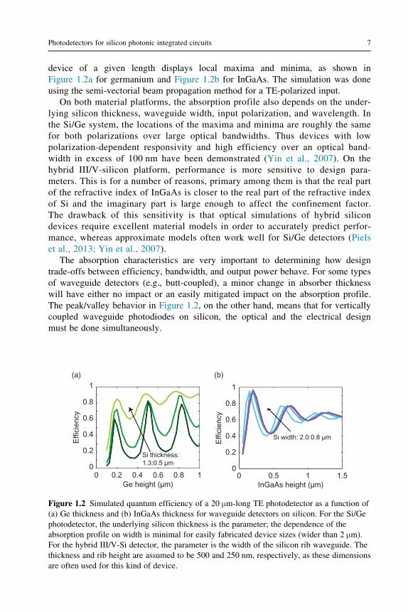
device of a given length displays local maxima and minima, as shown in
Figure 1.2a for germanium and Figure 1.2b for InGaAs. The simulation was done
using the semi-vectorial beam propagation method for a TE-polarized input.
On both material platforms, the absorption profile also depends on the under-
lying silicon thickness, waveguide width, input polarization, and wavelength. In
the Si/Ge system, the locations of the maxima and minima are roughly the same
for both polarizations over large optical bandwidths. Thus devices with low
polarization-dependent responsivity and high efficiency over an optical band-
width in excess of 100 nm have been demonstrated (Yin et al., 2007). On the
hybrid III/V-silicon platform, performance is more sensitive to design para-
meters. This is for a number of reasons, primary among them is that the real part
of the refractive index of InGaAs is closer to the real part of the refractive index
of Si and the imaginary part is large enough to affect the confinement factor.
The drawback of this sensitivity is that optical simulations of hybrid silicon
devices require excellent material models in order to accurately predict perfor-
mance, whereas approximate models often work well for Si/Ge detectors (Piels
et al., 2013; Yin et al., 2007).
The absorption characteristics are very important to determining how design
trade-offs between efficiency, bandwidth, and output power behave. For some types
of waveguide detectors (e.g., butt-coupled), a minor change in absorber thickness
will have either no impact or an easily mitigated impact on the absorption profile.
The peak/valley behavior in Figure 1.2, on the other hand, means that for vertically
coupled waveguide photodiodes on silicon, the optical and the electrical design
must be done simultaneously.
1(a) (b)
0.8
0.6
Effi
cien
cy
0.4
0.2
0
1
0.8
0.6
Effi
cien
cy
0.4
0.2
00 0.2 0.4 0.6
Ge height (µm)
Si thickness:1.3:0.5 µm
Si width: 2.0:0.8 µm
0.8 1 0 0.5InGaAs height (µm)
1 1.5
Figure 1.2 Simulated quantum efficiency of a 20 μm-long TE photodetector as a function of
(a) Ge thickness and (b) InGaAs thickness for waveguide detectors on silicon. For the Si/Ge
photodetector, the underlying silicon thickness is the parameter; the dependence of the
absorption profile on width is minimal for easily fabricated device sizes (wider than 2 μm).
For the hybrid III/V-Si detector, the parameter is the width of the silicon rib waveguide. The
thickness and rib height are assumed to be 500 and 250 nm, respectively, as these dimensions
are often used for this kind of device.
7Photodetectors for silicon photonic integrated circuits
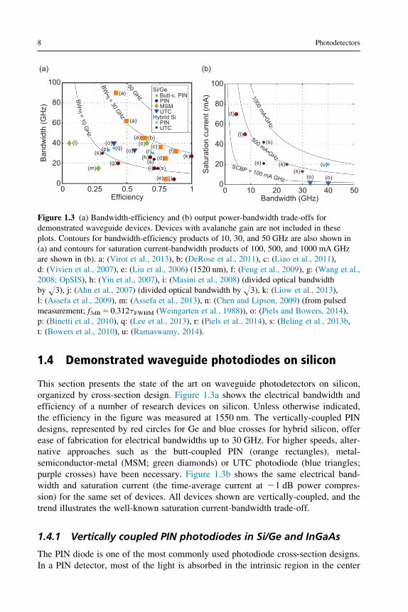
1.4 Demonstrated waveguide photodiodes on silicon
This section presents the state of the art on waveguide photodetectors on silicon,
organized by cross-section design. Figure 1.3a shows the electrical bandwidth and
efficiency of a number of research devices on silicon. Unless otherwise indicated,
the efficiency in the figure was measured at 1550 nm. The vertically-coupled PIN
designs, represented by red circles for Ge and blue crosses for hybrid silicon, offer
ease of fabrication for electrical bandwidths up to 30 GHz. For higher speeds, alter-
native approaches such as the butt-coupled PIN (orange rectangles), metal-
semiconductor-metal (MSM; green diamonds) or UTC photodiode (blue triangles;
purple crosses) have been necessary. Figure 1.3b shows the same electrical band-
width and saturation current (the time-average current at 21 dB power compres-
sion) for the same set of devices. All devices shown are vertically-coupled, and the
trend illustrates the well-known saturation current-bandwidth trade-off.
1.4.1 Vertically coupled PIN photodiodes in Si/Ge and InGaAs
The PIN diode is one of the most commonly used photodiode cross-section designs.
In a PIN detector, most of the light is absorbed in the intrinsic region in the center
100
(a) (b)
80
60
40
Ban
dwid
th (G
Hz)
20
0
100
80
60
40
Sat
urat
ion
curr
ent (
mA
)
20
00 10 20 30
Bandwidth (GHz)40 500 0.25
(l)
(m)
(s)
(g)
(p)(o)
(o)(q)
(a)
(a)
Si/GeButt-c. PINPINMSMUTC
Hybrid SiPINUTC
(a)
(n)
(h)(r)
(c)(b)
(s)(i) (s)
(e) (j)
(d)(f)
(t)
(t)(s)
1000 mA•G
Hz500 mA•GHz
(s)SCBP = 100 mA GHz
(s)(s)
(o) (o)
(u)(k)
0.5Efficiency
0.75 1
BW•η = 10 G
Hz
BW•η = 30 GHz
50 GHz
Figure 1.3 (a) Bandwidth-efficiency and (b) output power-bandwidth trade-offs for
demonstrated waveguide devices. Devices with avalanche gain are not included in these
plots. Contours for bandwidth-efficiency products of 10, 30, and 50 GHz are also shown in
(a) and contours for saturation current-bandwidth products of 100, 500, and 1000 mA GHz
are shown in (b). a: (Virot et al., 2013), b: (DeRose et al., 2011), c: (Liao et al., 2011),
d: (Vivien et al., 2007), e: (Liu et al., 2006) (1520 nm), f: (Feng et al., 2009), g: (Wang et al.,
2008; OpSIS), h: (Yin et al., 2007), i: (Masini et al., 2008) (divided optical bandwidth
by O3), j: (Ahn et al., 2007) (divided optical bandwidth by O3), k: (Liow et al., 2013),
l: (Assefa et al., 2009), m: (Assefa et al., 2013), n: (Chen and Lipson, 2009) (from pulsed
measurement; f3dB5 0.312τFWHM (Weingarten et al., 1988)), o: (Piels and Bowers, 2014),
p: (Binetti et al., 2010), q: (Lee et al., 2013), r: (Piels et al., 2014), s: (Beling et al., 2013b,
t: (Bowers et al., 2010), u: (Ramaswamy, 2014).
8 Photodetectors
of the device. For bandwidth, PIN design involves balancing the RC and the transit
time limit. The RC limit is approximately
fRC 51
2πðRs 1RLÞC(1.1)
where Rs is the diode series resistance, RL is the load resistance (typically 50 Ω),and C is the diode capacitance, and the transit time limit is about (Bowers and
Burrus, 1987)
fτ 50:45v
W(1.2)
where v is the smaller of the saturated electron and hole velocities and W is the
intrinsic region thickness. Since the diode capacitance is approximately εA/W,
where A is the diode area, there is an optimum intrinsic region thickness.
For vertically-coupled PIN photodiodes, the highest bandwidth-efficiency pro-
ducts can be obtained by choosing an absorption region thickness at a peak in
Figure 1.2. This is shown for a Si/Ge PIN as a surface plot in Figure 1.4a. The
calculation includes the transit time and RC limits assuming a 50 Ω load, but
neglects parasitic effects. The capacitance was calculated using a parallel plate
model and a device width of 3 μm. The germanium region was assumed to be
completely depleted for both bandwidth estimates (i.e., the thicknesses of the p-
and n-contact were assumed negligible or had negligible absorption due to larger
bandgap contact layers). The silicon waveguide height was 500 nm. The maxi-
mum values of bandwidth-efficiency product in Figure 1.4a are limited to below
60
(a) (b)
60
50
40
30
20
10
00
0
0.5
Effi
cien
cy
1
0.2 0.4 0.6Ge thickness (µm)
0.8 1
40
20
BW
. η
(GH
z)
BW
. η,
BW
(G
Hz)
40
30
20
10
0 0
0.5
1
0
Ge thickness (µm)
PD length (µm)
Figure 1.4 (a) Bandwidth-efficiency product for a vertically-coupled Si/Ge PIN photodiode
as a function of intrinsic region thickness and device length. The assumed width is 3 μm. (b)
Bandwidth, efficiency, and bandwidth-efficiency product for a 30 μm3 3 μm vertically-
coupled Si/Ge PIN photodiode as a function of intrinsic region thickness.
9Photodetectors for silicon photonic integrated circuits
60 GHz because the optimum thicknesses for fast absorption do not necessarily
correspond to thicknesses where the RC and transit time constants have been care-
fully balanced. This is shown (under the same assumptions used in Figure 1.4a) in
Figure 1.4b for a 30 μm long device. For maximum bandwidth, the optimum ger-
manium region thickness is 300 nm, but for maximum efficiency, 200 and 400 nm
give better performance.
Despite these difficulties, several devices with good performance have been
demonstrated. The largest demonstrated bandwidth of a vertically-coupled PIN pho-
todiode on Si/Ge is 27 GHz (Liow et al., 2013). Two Intel NIP photodiodes (Yin
et al., 2007) had responsivities of 0.89 and 1.16 A/W at 1550 nm and electrical
bandwidths of 26 and 24.1 GHz. A Luxtera device performed similarly, with a
responsivity of 0.85 A/W and bandwidth of 26 GHz (Masini et al., 2008). Finally,
IME demonstrated photodetectors with a 20 GHz bandwidth and 0.54 A/W respon-
sivity (Wang et al., 2008; OpSIS). The same group has recently demonstrated detec-
tors with improved responsivity and the same bandwidth using (low-field)
avalanche multiplication (Liow et al., 2013), and extended the 3 dB bandwidth by
using inductive gain peaking (Novack et al., 2013). It has proven difficult to
increase the bandwidth of a vertically coupled germanium PIN beyond 30 GHz in a
50 Ω environment while maintaining high efficiency.
The design space and results for hybrid III/V-silicon PIN photodetectors are
similar to those for Si/Ge photodetectors. Optically, although the absorption pro-
file can be altered by changing the width of the underlying silicon, achieving a
large change in confinement factor requires a very narrow waveguide, which in
turn requires lithography with higher resolution than what has historically been
used to fabricate this kind of device. Electrically, the transit time-limited band-
width of an InGaAs-based PIN detector is slightly lower and the RC-limited band-
width is slightly higher than the same quantities for an equivalent Si/Ge PIN. This
is because the hole velocity in InGaAs is slower than the carrier velocities in Ge,
increasing the transit time, and the dielectric constant is lower, which decreases
the capacitance. The performance of demonstrated devices is also similar to the
performance of Si/Ge PINs; a number of different devices have been demon-
strated, and the bandwidths were all around 30 GHz (Binetti et al., 2010; Lee
et al., 2013; Piels et al., 2014; Ramaswamy, 2014).
Both Si/Ge and hybrid III/V-silicon PIN detectors have been investigated for use
in high-power applications. The main limitations on output power are the active
area of the device and the maximum current density the cross-section can sustain
before the internal field collapses (Williams and Esman, 1999). In the intrinsic
region of a photodetector, under low-injection conditions, there is a roughly con-
stant electric field due to the applied bias that separates the charge carriers. As the
current density in the intrinsic region increases, the carriers screen the electric field.
Under high injection, the field distribution redistributes with the minimum occur-
ring in the intrinsic region. The maximum current density is reached when the mini-
mum of the electric field drops below the value necessary for the carriers to be able
to maintain their saturation velocities. For a PIN photodetector, this can be
expressed as (Piels, 2013)
10 Photodetectors
Jmax 56εvnvp
W2ðvn 1 vpÞðVbi 1VPD 2EcritWÞ (1.3)
where ε is the dielectric constant of the intrinsic region, vn and vp are the saturated
electron and hole velocities, W is the intrinsic region width, Vbi is the diode built-in
voltage, VPD is the voltage drop across the device due to the load resistance and
applied bias, and Ecrit is the electric field at which the carrier velocities saturate.
The factor 6εvnvp=W2i ðvn 1 vpÞ determines how the saturation current scales with
bias voltage, and should be as large as possible for high-power conversion effi-
ciency (Tulchinsky et al., 2008). In germanium, it is 2.6e2 5 A/V/cm2, while for
InGaAs it is 2.3e2 5 A/V/cm2, and so we expect slightly better power handling
from a Si/Ge PIN than from an InGaAs PIN with the same dimensions at the same
bias voltage. However, the breakdown field of InGaAs is about twice that of Ge, so
in the absence of a system limit on bias voltage (and neglecting thermal effects),
the InGaAs device would have a larger saturated output power.
1.4.2 Butt-coupled PIN photodiodes in Ge
One approach to increasing the bandwidth beyond 30 GHz is to use a butt-coupled
or nearly butt-coupled design (Virot et al., 2013; DeRose et al., 2011; Liao et al.,
2011; Vivien et al., 2007; Feng et al., 2009). The confinement factor in the germa-
nium for these photodiodes is nearly 100% regardless of the total germanium thick-
ness used. As a result, most of the light can be absorbed by very short (less than
10 μm long) devices. The highest bandwidths for waveguide photodiodes on silicon
to date have been reported for ultra-compact butt-coupled PIN detectors.
The optical characteristics of the device are relatively insensitive to the germa-
nium thickness and device width, so a large degree of electrical optimization is pos-
sible. Due to their small size, the capacitance of ultra-compact devices is usually
very small, regardless of the intrinsic region thickness. This enables the use of very
thin intrinsic regions for decreased transit time and operating voltage. There is a
significant fabrication challenge in getting the contact resistance low enough for
high bandwidth in a 50 Ω environment, but in large part these are being advocated
for applications where a larger series resistance may be acceptable. The primary
disadvantage of such ultra-compact designs comes in power handling. Due to the
small active device area, the maximum output power is expected to be low.
1.4.3 MSM photodetectors
Another way to increase the bandwidth is to use a cross-section design with lower
capacitance per unit area. MSM detectors have this property, and have been demon-
strated on Si/Ge. IBM successfully integrated a germanium-based photodiode with
a 38 GHz bandwidth into a CMOS process flow, though the responsivity at
1550 nm was only 0.07 A/W (Assefa et al., 2009). The same group integrated simi-
lar devices with higher responsivity and lower bandwidth with TIAs (Assefa et al.,
11Photodetectors for silicon photonic integrated circuits
2013). They also showed that it is possible to use such a structure in avalanche
mode at low (1.5 V) bias, which yields a significant sensitivity improvement, while
maintaining a 30 GHz bandwidth (Assefa et al., 2010c). Chen and Lipson demon-
strated a device with 40 GHz bandwidth and higher (0.35 A/W) responsivity fabri-
cated using wafer-bonding (Chen and Lipson, 2009). For both devices, because the
germanium is not grown on silicon using CVD, the responsivity begins to roll off at
relatively short wavelengths. In general, MSM devices can have lower capacitance
per unit area than PIN detectors because the depletion region only occupies a frac-
tion of the device area. One consequence of this is that the saturation current den-
sity is also decreased. In addition, the dark current of MSM detectors is often
higher than the dark current of PIN diode-based devices.
1.4.4 SACM avalanche photodiodes
For the lowest noise receivers, photodetectors with gain are attractive, using either
avalanche or photoconductive gain. Silicon is an excellent material for avalanche
gain due to the low electron and hole ionization coefficient ratio (k, 0.1), which
allows for high gain-bandwidth products and low excess noise factors. SACM ava-
lanche photodetectors (APDs) using silicon avalanche regions have been demon-
strated using both III-V (Hawkins et al., 1997) and Ge (Dai et al., 2010) absorbing
regions. In the surface-normal configuration, gain-bandwidth products up to
840 GHz (Sfar Zaoui et al., 2009) have been demonstrated in for Si/Ge devices and
up to 315 GHz (Hawkins et al., 1997) have been demonstrated for III-V/Si ones. As
waveguide detectors, the highest gain-bandwidth product was at least 380 GHz
(Duan et al., 2013) (20 GHz, gain. 19).
1.4.5 Si/Ge UTC photodiodes
The UTC cross-section is an alternative way to push the bandwidth of a waveguide
Si/Ge photodiode beyond 30 GHz in a vertically-coupled configuration without
decreasing the active device area. A UTC is a decoupled structure where the
absorption occurs in a doped layer and carriers are collected through a depleted
layer in the silicon. As a result, the germanium thickness can be chosen for optimal
coupling from the silicon waveguide without affecting the capacitance, and
vertically-coupled devices with relatively large footprints and fast transit times can
be fabricated without sacrificing RC performance. Recently, Si/Ge UTCs with a
bandwidth of 40 GHz and responsivity of 0.5 A/W have been demonstrated (Piels
and Bowers, 2014).
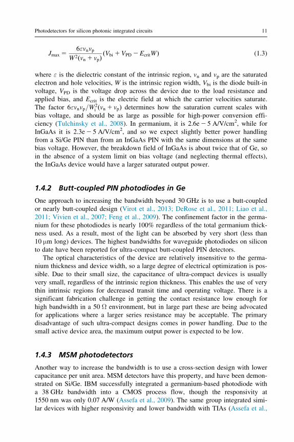
The cross-section and band diagram of the devices in Piels and Bowers (2014)
are shown in Figure 1.5. The transit time is dominated by minority electron trans-
port through the absorber and collector (holes in the absorber move to screen the
minority charges), which is the origin of the term uni-traveling (Ishibashi et al.,
1997). In the absorber, photogenerated carriers move toward the collector by a com-
bination of diffusion and drift; the absorber is doped on a grade to produce a small
electric field and decrease the transit time. In the collector, injected minority
12 Photodetectors
electrons form a drift current (from the electric field due to the bias voltage) and
are collected at the n-contact. Unlike PIN diodes in Si/Ge, UTC detectors perform
better when they are p-side up. The threading defects that form at the Si/Ge hetero-
interface pin the Fermi level in that region, but if the germanium is doped suffi-
ciently highly, this does not result in the formation of a large barrier (Piels and
Bowers, 2014).
UTC photodiodes were first demonstrated in III/V materials, where they have
been shown to have superior bandwidth and power handling due to the large elec-
tron velocity in InP relative to the hole velocity. In group IV materials, electron and
hole velocities are similar, and the benefit of the UTC is instead that it allows us to
choose a capacitance per unit area independently from the absorbing region thick-
ness. For the absorption peak at 200 nm Ge thickness, this results in a higher
bandwidth-efficiency product. In a UTC photodiode, the transit time is dominated
by the electron transport properties and the capacitance is dominated by the collec-
tor thickness. The material constants in Eqs (1.1) and (1.2) change, and Eq. (1.3)
becomes (Mishra and Singh, 2008)
Jmax 52εvnW2
ðVbi 1VPD 2EcritWÞ (1.4)
where ε now refers to the dielectric constant of the silicon collector and W is its
thickness.
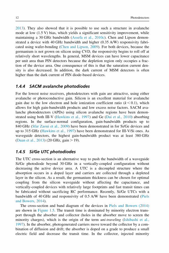
Figure 1.6a shows idealized design curves for bandwidth and efficiency for PIN
and UTC photodiodes assuming a 200 nm thick absorber and a 3 μm wide mesa.
Parasitic effects (e.g., pad capacitance and diode series resistance) are neglected in
the simulation. The collector thickness of the UTC was chosen separately for each
detector length to maximize the bandwidth-efficiency product. As the figure shows,
for even moderate efficiency, the UTC out-performs the PIN. Figure 1.6b shows the
calculated saturation current-bandwidth product for 3 μm3 30 μm PIN and UTC
photodiodes as a function of intrinsic region thickness (Ge for the PIN, Si for the
UTC). The assumed bias voltage is half the breakdown voltage of the diode, and
the illumination profile was assumed uniform (this will result in an optimistic
Figure 1.5 (a) Band diagram and (b) cross-section schematic of a waveguide Si/Ge uni-
traveling carrier photodetector.
Source: Reprinted with permission from Piels and Bowers (2014).
13Photodetectors for silicon photonic integrated circuits
estimate of the saturation current). Parasitic effects were again ignored. The UTC
has both higher saturation current and higher bandwidth, which leads to higher esti-
mated saturation-current bandwidth products.
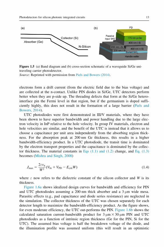
In Piels and Bowers (2014), high-speed (.33 GHz) waveguide-type Ge/Si UTC
photodiodes with dilute absorption profiles were demonstrated with high responsiv-
ities (.0.5 A/W) and high 1 dB-compression (.1.5 mA). Figure 1.7a shows the fre-
quency responses of a 3 μm3 90 μm and a 4 μm3 13 μm device at 22 and 25 V
bias. The frequency response was measured with an Agilent lightwave component
analyzer at 1550 nm and includes the effect of the probe pad impedance. At 25 V
bias, the 3 dB electrical bandwidth of the 3 μm3 90 μm detector was 33 GHz while
for the 4 μm3 13 μm detector, it was 40 GHz. The corresponding optical bandwidths
(i.e., 10 log10(S21)) of the two devices are 54 and 56 GHz, respectively.
Figure 1.6 (a) BW-efficiency product and (b) saturation current-bandwidth product (SCBP)
for ideal PIN and UTC photodiodes assuming 200 nm Ge thickness and a 3 μm wide mesa.
2 0
–10
–20
–30
–40
–5010–4 10–3
Photocurrent (A)10–2
Out
put p
ower
(dB
m)
(a) (b)
0
2 V5 V 5 V
5 V
3 V
3 V
1 V
1 V
4 X 13
3 X 90
3 X 90
4 X 13
–2
Res
pons
e (d
B)
–4
–6
–80 20 40
Frequency (GHz)60
Figure 1.7 (a) Bandwidth and (b) power handling of Si/Ge UTC photodetectors at 30 GHz.
Source: Reprinted with permission from Piels and Bowers (2014).
14 Photodetectors
The large-signal saturation characteristics of the 40 GHz 4 μm3 13 μm and the
33 GHz 3 μm3 90 μm devices discussed above are shown in Figure 1.7b. An 80%
modulation depth tone fixed at 30 GHz was generated using the standard hetero-
dyne technique with two free-running lasers at 1537 nm. The RF power was mea-
sured on an electrical spectrum analyzer. The loss of the cables was measured with
a network analyzer and subtracted from the data. In both cases, the 21 dB
compression current is around 2 mA, which corresponds to an output power around
220 dBm. However, the longer device has larger maximum output power since the
output power continues to increase after the 21 dB compression current is reached.
This is because the back of the device continues to operate in the linear regime
even when the front of the device is compressed, whereas for the shorter device, the
current is more uniformly distributed. This leads to a sharp decrease in output
power beyond the 21 dB compression current for the shorter device, in contrast to
a slow increase in output power for the longer one. The maximum output power of
the 4 μm3 13 μm detector at 30 GHz is 221.4 dBm, while it is 211.7 dBm for the
longer one. Si/Ge UTCs are thus promising for use in high-power high-speed appli-
cations. At present, the primary limitation to both bandwidth and power handling is
carrier transport through the heterojunction; improved performance can be expected
as the growth technology matures.
1.4.6 Hybrid III/V-silicon UTC photodiodes
UTC designs can also be used to increase the bandwidth and output power of
hybrid III/V-silicon photodiodes. Figure 1.8 shows a cross-section of a fabricated
P-contact P-contact
Si rib WG
Buried oxide
N-contact
InP, n.i.d, <5.0 x 10¹⁵, 700 nm
InGaAs, C, 8 x 10¹⁹ – 5 x 10¹⁸, 250 nm
InGaAs, n.i.d, <5.0 x 10¹⁵, 50 nm
InP Matching Layer, p+, Be, 8 x 10¹⁸, 100 nm
InP, n+, Si, 3.0 x 10¹⁹, 100 nm
InP, Si, 1 x 10¹⁷, 10 nmInGaAs/InAIAs chirped Superlattice,
n.i.d, <5.0 x 10¹⁵, 24 nm
Figure 1.8 Layer stack and cross-section schematic of the hybrid III/V-silicon MUTC
photodiode. Doping concentrations are in cm23.
Source: Reprinted with permission from Beling et al. (2013a).
15Photodetectors for silicon photonic integrated circuits
device (Beling et al., 2013b); it is based on a surface-normal structure that had
high bandwidth and high saturated output power (Li et al., 2011). The modified
uni-traveling carrier (MUTC) differs from the UTC in that part of the absorbing
region closest to the collector is left undoped. The bias voltage thus induces an
electric field in the area of the heterojunction, which improves the carrier trans-
port properties, increasing linearity and bandwidth. The ability to do band engi-
neering is a strong difference between the hybrid III/V-Si platform and Si/Ge
platform, and we see much better performance for HSP UTCs than for Si/Ge
UTCs.
Beling et al. (2013a,b) report on high-speed high-power waveguide MUTC PDs
on the hybrid silicon platform with internal responsivities up to 0.85 A/W.
Figure 1.9a shows the measured bandwidths of three devices with different lengths
(25, 50, and 100 μm) and a 14 μm wide mesa. The bandwidth was measured using
an optical heterodyne setup with a modulation depth close to 100%. For the shortest
(25 μm) device, the 3 dB bandwidth was 30 GHz. Figure 1.9b shows the RF output
power and compression of this device as a function of time-average photocurrent
for the shortest device at 30 GHz. The maximum at 30 GHz was 3.9 dBm, while at
20 GHz it was 5.6 dBm.
To increase the RF output power, photodiode arrays were designed and fab-
ricated. Optically, the input was distributed to multiple diodes via a multimode
interferometer as shown in Figure 1.10a. Electrically, the signals were summed
in parallel at the probe pads. At 20 GHz, a two-photodiode array achieved an
RF output power of 9.3 dBm, while a four-detector array achieved an RF out-
put power of 10.2 dBm. The performance was limited by the available input
power; in principle, higher output power is possible. For both arrays, the RF
output power exceeded that of the single photodiodes discussed above, which
indicates the promise of this approach for increasing the output power avail-
able from a PIC.
3
(a) (b)
0
–3
–6
–9
–12
–150 10
2550100
20Frequency (GHz)
30 40
RF
out
put p
ower
(dB
m)
RF
com
pres
sion
(dB
)
5 543210–1–2–3–4
0–5
–10–15–20–25–30–35–40
0.1 1
Vbias=3 VVbias=4 VVbias=5 VVbias=6 VVbias=7 V
Average photocurrent (mA)10
Rel
ativ
e re
spon
se (
dB)
Figure 1.9 (a) Bandwidth and (b) RF output power for hybrid III/V-silicon modified UTCs.
Source: Reprinted with permission from Beling et al. (2013a).
16 Photodetectors
1.5 Conclusions and future outlook
We have presented an overview of photodetectors heterogeneously integrated on
silicon-on-insulator. For very high-speed applications where output power is not of
great concern, ultra-compact butt-coupled Si/Ge PINs have the best bandwidth and
efficiency. For microwave photonics and coherent communication applications
requiring large photocurrents, vertically-coupled UTC detectors, either on the
hybrid III/V-silicon platform or in Si/Ge, are preferable. Both of these technologies
are in their initial stages of development, and can be further improved. The band
engineering currently available in III/V (that has been critical to enhancing III/V
MUTC performance) can be applied to the Si/Ge UTC as germanium-on-silicon
growth technology matures. Advanced optical designs (Beling et al., 2013a,b) can
be applied to both platforms, further increasing output power.
References
Ahn, D., Hong, C.-Y., Liu, J., Giziewicz, W., Beals, M., Kimerling, L.C., et al., 2007. High
performance, waveguide integrated Ge photodetectors. Opt. Express. 15 (7), 3916�3921.
Assefa, S., Xia, F., Bedell, S.W., Zhang, Y., Topuria, T., Rice, P.M., et al., 2009. CMOS-
integrated 40 GHz germanium waveguide photodetector for on-chip optical intercon-
nects. In: Optical Fiber Communication Conference and National Fiber Optic Engineers
Conference, San Diego, CA.
Assefa, S., Xia, F., Bedell, S.W., Zhang, Y., Topuria, T., Rice, P.M., et al., 2010a. CMOS-
integrated high-speed MSM germanium waveguide photodetector. Opt. Express. 18 (5),
4986�4999.
Assefa, S., Xia, F., Green, W., Schow, C., Rylyakov, A., Vlasov, Y., 2010b. CMOS-
integrated optical receivers for on-chip interconnects. IEEE J. Sel. Top. Quantum
Electron. 16 (5), 1376�1385.
15
10
5
0(c)
(a) (b)
–5
–101 10
Average photocurrent (mA)
2.3 mm long MMI splitter
2-PD array4-PD array
100
RF
out
put p
ower
(dB
m)
Figure 1.10 MMI-fed photodiode array (a) operating principle and (b) RF output power at
20 GHz as a function of average photocurrent for arrays of 10 μm3 37 μm photodetectors.
Source: Reprinted with permission from Beling et al. (2013a).
17Photodetectors for silicon photonic integrated circuits
Assefa, S., Xia, F., Vlasov, Y.A., 2010c. Reinventing germanium avalanche photodetector
for nanophotonic on-chip optical interconnects. Nature. 464, 80�84.
Assefa, S., Pan, H., Shank, S., Green, W., Rylyakov, A., Schow, C., et al., 2013.
Monolithically integrated silicon nanophotonics receiver in 90 nm CMOS technology
node. In: Optical Fiber Communication Conference/National Fiber Optic Engineers
Conference, Anaheim, CA.
Beling, A., Cross, A.S., Piels, M., Peters, J., Fu, Y., Zhou, Q., et al., 2013a. High-power
high-speed waveguide photodiodes and photodiode arrays heterogeneously integrated on
silicon-on-insulator. In: Optical Fiber Communication Conference/National Fiber Optic
Engineers Conference, Anaheim, CA.
Beling, A., Cross, A., Piels, M., Peters, J., Zhou, Q., Bowers, J., et al., 2013b. InP-based
waveguide photodiodes heterogeneously integrated on silicon-on-insulator for photonic
microwave generation. Opt. Express. 21 (22), 25901�25906.
Binetti, P., Leitjens, X.J.M., de Vries, T., Oei, Y.S., Di Cioccio, L., Fedeli, J.M., et al., 2010.
InP/InGaAs photodetector on SOI photonic circuitry. IEEE Photonics J. 2 (3), 299�305.
Black, A., Hawkins, A.R., Margalit, N.M., Babic, D.I., Holmes Jr., A.L., Chang, Y.-L., et al.,
1997. Wafer fusion: materials issues and device results. IEEE J. Sel. Top. Quantum
Electron. 3 (3), 943�951.
Bowers, J.E., Burrus, C.A., 1986. High speed zero bias waveguide photodetectors. Electron.
Lett. 22 (17), 905.
Bowers, J.E., Burrus, C., 1987. Ultrawide-band long-wavelength p-i-n photodetectors.
J. Lightwave Technol. LT-5 (10), 1339�1350.
Bowers, J.E., Piels, M., Ramaswamy, A., Yin, T., 2010. High power waveguide Ge/Si photo-
diodes. In: Annual Meeting of the Electrochemical Society, Las Vegas, NV.
Chang, H., Kuo, Y., Jones, R., Barkai, A., Bowers, J.E., 2010. Integrated hybrid silicon
triplexer. Opt. Express. 18 (23), 23891�23899.
Chen, L., Lipson, M., 2009. Ultra-low capacitance and high speed germanium photodetectors
on silicon. Opt. Express. 17 (10), 7901�7906.
Chen, R., Tran, T.-T.D., Ng, K.W., Ko, S.W., Chuang, L.C., Sedgwick, F.G., et al., 2011.
Nanolasers grown on silicon. Nat. Photonics. 5, 170�175.
Dai, D., Chen, H.-W., Bowers, J.E., Kang, Y., Morse, M., Paniccia, M., 2010. Equivalent
circuit model of a waveguide-type Ge/Si avalanche photodetector. Phys. Status Solidi C.
7 (10), 2532�2535.
Dai, D., Piels, M., Bowers, J.E., 2014. Monolithic Germanium/Silicon photodetectors with
decoupled structures: resonant APDs and UTC photodiodes. J. Sel. Top. Quantum
Electron. 20 (6), 3802214.
DeRose, C.T., Trotter, D.C., Zortman, W.A., Starbuck, A.L., Fisher, M., Watts, M.R., et al.,
2011. Ultra compact 45 GHz CMOS compatible germanium waveguide photodiode with
low dark current. Opt. Express. 19 (25), 24897�24904.
Duan, N., Liow, T.-Y., Lim, A., Ding, L., Lo, G., 2013. High speed waveguide-integrated
Ge/Si avalanche photodetector. In: Optical Fiber Communication Conference, Anaheim,
CA, United States.
Feng, D., Liao, S., Dong, P., Feng, N.-N., Liang, H., Zheng, D., et al., 2009. High-speed Ge
photodetector monolithically integrated with large cross-section silicon-on-insulator
waveguide. Appl. Phys. Lett. 95 (26), 261105�261105-3.
Feng, S., Geng, Y., Lau, K.M., Poon, A.W., 2012. Epitaxial III-V-on-silicon waveguide butt-
coupled photodetectors. Opt. Lett. 37 (19), 4035�4037.
Galland, C., Novack, A., Liu, Y., Ding, R., Gould, M., Baehr-Jones, T., et al., 2013.
A CMOS-compatible silicon photonic platform for high-speed integrated opto-
electronics, 87670G-1. Proc. SPIE, 8767.
18 Photodetectors
Giovane, L.M., Luan, H.-C., Agarwal, A., Kimerling, L.C., 2001. Correlation between leak-
age current density and threading dislocation density in SiGe p-i-n diodes grown on
relaxed graded buffer layers. Appl. Phys. Lett. 78, 541�543.
Hartmann, J., Damlencourt, J.-F., Bogumilowicz, Y., Holliger, P., Rolland, G., Billon, T., 2005.
Reduced pressure-chemical vapor deposition of intrinsic and doped Ge layers on Si(001)
for microelectronics and optoelectronics purposes. J. Cryst. Growth. 274 (1�2), 90�99.
Hawkins, A.R., Wu, W., Abraham, P., Streubel, K., Bowers, J.E., 1997. High gain-
bandwidth-product silicon heterointerface photodetector. Appl. Phys. Lett. 70, 303�305.
Heck, M.J.R., Bauters, J.F., Davenport, M.L., Doylend, J.K., Jain, S., Kurczveil, G., et al.,
2013. Hybrid silicon photonic integrated circuit technology. IEEE J. Sel Top. Quantum
Electron. 19 (4), 6100117.
Højfeldt, S., Mørk, J., 2002. Modeling of carrier dynamics in quantum-well electroabsorption
modulators. IEEE J. Sel. Top. Quantum Electron. 8 (6), 1265�1276.
Ishibashi, T., Shimizu, N., Kodama, S., Ito, H., Nagatsuma, T., Furuta, T., 1997. Uni-traveling-
carrier photodiodes. In: Ultrafast Electronics and Optoelectronics, Incline Village, NV.
Knights, A.P., Doylend, J.K., 2008. Silicon photonics � recent advances in device develop-
ment. Advances in Information Optics and Photonics. SPIE Press, pp. 633�656.
Koch, B., Norberg, E., Kim, B., Hutchinson, J., Shin, J., Fish, G., et al., 2013. Integrated sili-
con photonic laser sources for telecom and datacom. In: Optical Fiber Communication
Conference/National Fiber Optic Engineers Conference, Anaheim, CA.
Lee, B., Rylyakov, A., Proesel, J., Baks, C., Rimolo-Donadio, R., Schow, C., et al., 2013.
60-Gb/s receiver employing heterogeneously integrated silicon waveguide coupled
photodetector. In: CLEO: 2013 Postdeadline, San Jose, CA.
Li, Z., Fu, Y., Piels, M., Pan, H., Beling, A., Bowers, J.E., et al., 2011. High-power high-lin-
earity flip-chip bonded modified uni-traveling carrier photodiode. Opt. Express. 19 (26),
B385�B390.
Liao, S., Feng, N.-N., Feng, D., Dong, P., Shafiiha, R., Kung, C.-C., et al., 2011. 36 GHz
submicron silicon waveguide germanium photodetector. Opt. Express. 19 (11),
10967�10972.
Liow, T.-Y., Lim, A.E., Duan, N., Yu, M., Lo, G., 2013. Waveguide germanium photodetec-
tor with high bandwidth and high L-band responsivity. In: Optical Fiber Communication
Conference/National Fiber Optic Engineers Conference, Anaheim, CA.
Liu, J., Cannon, D.D., Wada, K., Ishikawa, Y., Danielson, D.T., Jongthammanurak, S., et al.,
2004. Deformation potential constants of biaxially tensile stressed Ge epitaxial films on
Si(100). Phys. Rev. B. 70 (15), 155309.
Liu, J., Ahn, D., Hong, C.Y., Pan, D., Jongthammanurak, S., Beals, M., et al., 2006.
Waveguide integrated Ge p-i-n photodetectors on a silicon-oninsulator platform. In:
Optics Valley of China International Symposium on Optoelectronics.
Liu, A.Y., Zhang, C., Norman, J., Snyder, A., Lubyshev, D., Fastenau, J.M., et al., 2014.
High performance continuous wave 1.3 μm quantum dot lasers on silicon. Appl. Phys.
Lett. 104, 041104.
Marris-Morini, D., Virot, L., Baudot, C., Fedeli, J., Rasigade, G., Perez-Galacho, D., et al.,
2014. A 40 Gbit/s optical link on a 300-mm silicon platform. Opt. Express. 22 (6),
6674�6679.
Masini, C., Colace, L., Assanto, G., Luan, H.-C., Kimerling, L.C., 2001. High performance
p-i-n Ge on Si photodetectors for the near infrared: from model to demonstration. IEEE
Trans. Electron Devices. 48 (6), 1092�1096.
Masini, G., Sahni, S., Capellini, G., Witzens, J., Gunn, C., 2008. High-speed near infrared
optical receivers based on Ge waveguide photodetectors integrated in a CMOS process.
Adv. Opt. Technol. 2008, 196572.
19Photodetectors for silicon photonic integrated circuits
Michel, J., Liu, J., Kimerling, L.C., 2010. High-performance Ge-on-Si photodetectors. Nat.
Photonics. 4 (8), 527�534.
Mishra, U.K., Singh, J., 2008. Semiconductor Device Physics and Design. Springer-Verlag,
AA Dordrecht, the Netherlands.
Mueller, R.K., 1959. Dislocation acceptor levels in germanium. J. Appl. Phys. 30 (12),
2015�2016.
Novack, A., Gould, M., Yang, Y., Xuan, Z., Streshinsky, M., Liu, Y., et al., 2013.
Germanium photodetector with 60 GHz bandwidth using inductive gain peaking. Opt.
Express. 21 (23), 28387�28393.
OpSIS, OpSIS-IME O150 process performance summary.
Park, H., Fang, A., Jones, R., Cohen, O., Raday, O., Sysak, M., et al., 2007. A hybrid
AlGaInAs-silicon evanescent waveguide photodetector. Opt. Express. 15 (6), 6044�6052.
Piels, M., 2013. Si/Ge Photodiodes for Coherent and Analog Communication. University of
California, Santa Barbara, CA.
Piels, M., Bowers, J., 2014. 40 GHz Si/Ge uni-traveling carrier waveguide photodiode.
J. Lightwave Technol. 32 (20), 3502�3508.
Piels, M., Ramaswamy, A., Bowers, J., 2013. Nonlinear modeling of waveguide photodetec-
tors. Opt. Express. 21, 15634�15644.
Piels, M., Bauters, J.F., Davenport, M.L., Heck, M.J.R., Bowers, J.E., 2014. Low-loss silicon
nitride AWG demultiplexer heterogeneously integrated with hybrid III-V/Silicon photo-
detectors. J. Lightwave Technol. 32 (4), 817�823.
Ramaswamy, A., 2014. Private communication.
Roucka, R., Mathews, J., Weng, C., Beeler, R., Tolle, J., Menendez, J., et al., 2011.
Development of high performance near IR photodiodes: a novel chemistry based approach
to Ge-Sn devices integrated on silicon. IEEE J. Quantum Electron. 47 (2), 213�222.
Sfar Zaoui, W., Chen, H.-W., Bowers, J.E., Bowers, J.E., Kang, Y., Morse, M., et al., 2009.
Frequency response and bandwidth enhancement in Ge/Si avalanche photodiodes with
over 840 GHz gain-bandwidth-product. Opt. Express. 17 (15), .
Tanabe, K., Watanabe, K., Arakawa, Y., 2012. III-V/Si hybrid photonic devices by direct
fusion bonding. Sci. Rep. 2, 349.
Tulchinsky, D.A., Boos, J.B., Park, D., Goetz, P.G., Rabinovich, W.S., Williams, K.J., 2008.
High-current photodetectors as efficient, linear, and high-power RF output stages.
J. Lightwave Technol. 26 (4), 408�416.
Virot, L., Vivien, L., Fedeli, J., Bogumilowicz, Y., Hartmann, J., Boeuf, F., et al., 2013.
High-performance waveguide-integrated germanium PIN photodiodes for optical com-
munication applications. Photonics Res. 1, 140�147.
Vivien, L., Rouviere, M., Fedeli, J.-M., Marris-Morini, D., Damlencourt, J.F., Mangeney, J.,
et al., 2007. High speed and high responsivity germanium photodetector integrated in a
silicon-on-insulator microwaveguide. Opt. Express. 15 (15), 9843�9848.
Wang, J., Loh, W.-Y., Chua, K., Zhang, H., Xiong, Y., Loh, T.H., et al., 2008. Evanescent-
coupled Ge p-i-n photodetectors on Si-waveguide with SEG-Ge and comparative study
of lateral and vertical p-i-n configurations. IEEE Electron Device Lett. 29 (5), 445�448.
Weingarten, K., Rodwell, M., Bloom, D., 1988. Picosecond optical sampling of GaAs inte-
grated circuits. IEEE J. Quantum Electron. 24 (2), 198�220.
Williams, K.J., Esman, R., 1999. Design considerations for high-current photodetectors.
J. Lightwave Technol. 17 (8), 1443�1454.
Yin, T., Cohen, R., Morse, M.M., Sarid, G., Chetrit, Y., Rubin, D., et al., 2007. 31 GHz Ge
n-i-p waveguide photodetectors on silicon-on-insulator substrate. Opt. Express. 15 (21),
13965�13971.
20 Photodetectors