1 · web viewbecause the mixer system was specified as a late addition to a previously...
TRANSCRIPT

Fermi National Accelerator Laboratory
D-Zero Detector Central Fiber Tracker (CFT) Axial ProjectReadout Electronics
Central Tracker Trigger (CTT) Mixer System
Date: April 1st, 2000Revision Date: February 28th, 2003
N. George Wilcer, S. Marco Rapisarda
Document # ESE-D0-000401

Central Tracker Trigger (CTT) Mixer System February 28th, 2003
Page 1

Central Tracker Trigger (CTT) Mixer System February 28th, 2003
Table of contents
1. People and acknowledgements...........................................................................................................72. Introduction........................................................................................................................................8
Figure 2.1, picture of the mixer system subrack...........................................................................................8Figure 2.2, Data flow..................................................................................................................................10
3. DAQ System Components................................................................................................................123.1 Front End Data Flow.................................................................................................................14
Figure 3.1, Front End data flow..................................................................................................................143.2 Supersector and Mixer Board Data Flow..................................................................................15
Figure 3.2, Supersector data flow...............................................................................................................16Figure 3.3, Mixer Board data flow.............................................................................................................17
3.3 Data frame structure and timing................................................................................................18Figure 3.4, Master clock, data timing and frame structure at the output of the LVDS receivers...............18
3.4 Mixer Board Block Diagram......................................................................................................19Figure 3.5, Mixer Board Block Diagram....................................................................................................21
4. Interfaces ........................................................................................................................................224.1 LVDS Links Inputs from AFEs....................................................................................................22
Figure 4.1, LVDS Input links logic block..................................................................................................22Table 4.1, Signal assignments for the LVDS inputs connector..................................................................23
4.2 LVDS Links Outputs to DFEs.....................................................................................................24Figure 4.2, LVDS Output links logic block................................................................................................24Table 4.2, Signal assignments for the LVDS outputs connector................................................................25
4.3 LVDS Cabling.............................................................................................................................26Figure 4.3, LVDS cabling.for a 28 bit wide link........................................................................................26Figure 4.4, 28 bit link (3x5) LVDS cable...................................................................................................26
4.4 Mixer System Backplane.............................................................................................................27Figure 4.5, Mixer System backplane..........................................................................................................28
4.5 Mixer Board - Subrack Controller General Purpose Bus interface...........................................29Figure 4.6, Address bits..............................................................................................................................29Table 4.3, Mixer System Subrack slot addressing......................................................................................29
4.5.1 Bus Signals.................................................................................................................................................30Figure 4.7, General Purpose Bus signals....................................................................................................30Table 4.4, General Purpose Bus signals.....................................................................................................30
4.5.2 Write and Read Cycles...............................................................................................................................31Figure 4.8, Write operation timing.............................................................................................................31Figure 4.9, Read operation timing..............................................................................................................32
4.5.3 Data Space Description...............................................................................................................................33Table 4.5, Data space address map.............................................................................................................33
4.5.4 Board Status/Control register.....................................................................................................................34Figure 4.10, Board Status/Control Register................................................................................................34Table 4.6, Board Status/Control Register...................................................................................................34
4.5.5 Device Status/Control register....................................................................................................................35Figure 4.11, Device Status/Control Register..............................................................................................35Table 4.7, Device Status/Control Register.................................................................................................36
4.5.6 Device Configuration Data register............................................................................................................36Figure 4.12, Device Configuration Data Register......................................................................................36
4.5.7 Device Firmware ID register......................................................................................................................36Figure 4.13, Firmware ID Register.............................................................................................................36Table 4.8, Device Firmware ID Register....................................................................................................37
4.5.8 Mode of Operation register.........................................................................................................................37Figure 4.14, Mode of Operation register....................................................................................................37Table 4.9, Mode of Operation Register......................................................................................................37
4.5.9 Input Links Error Status registers...............................................................................................................38Figure 4.15, Input Links Error Status Registers.........................................................................................38
Page 2

Central Tracker Trigger (CTT) Mixer System February 28th, 2003
Table 4.10, Input Links Error Status Low Register....................................................................................38Table 4.11, Input Links Error Status High Register...................................................................................38
4.5.10 Device Access-Address register.................................................................................................................39Figure 4.16, Device Access-Address register.............................................................................................39Table 4.12, Device Access-Address register..............................................................................................39
4.5.11 Device Access-Data register.......................................................................................................................39Figure 4.17, Device Access Data register...................................................................................................39Table 4.13, Device Access register.............................................................................................................39
4.5.12 Device Access Structure.............................................................................................................................40Figure 4.18, Device Access Structure.........................................................................................................40
4.5.13 Output Links Test Mode registers..............................................................................................................41Figure 4.19, DFE0 and DFE1 Output Links Test Mode Registers.............................................................41Table 4.14, DFE0 Output Links Test Mode Register.................................................................................41Table 4.15, DFE1 Output Links Test Mode Register.................................................................................41
4.5.14 Monitoring Mode register...........................................................................................................................42Figure 4.20, Monitoring Mode Register.....................................................................................................42Table 4.16, Monitoring Mode Register......................................................................................................42
4.5.15 Monitoring Status registers.........................................................................................................................43Figure 4.21, Monitoring Status Registers...................................................................................................43Table 4.17, Monitoring Status Low Register..............................................................................................43Table 4.18, Monitoring Status High Register.............................................................................................43
4.5.16 Monitoring Status History registers............................................................................................................44Figure 4.22, Monitoring Status History Registers......................................................................................44Table 4.19, Monitoring Status Low History Register.................................................................................44Table 4.20, Monitoring Status High History Register................................................................................44
4.5.17 Board Status/Control register B..................................................................................................................45Figure 4.23, Board Status/Control Register B............................................................................................45Table 4.21, Board Status/Control Register B.............................................................................................45
4.5.18 FIFO Trigger Control register....................................................................................................................45Figure 4.24, FIFO Trigger Control Register...............................................................................................45Table 4.22, FIFO Trigger Control Register................................................................................................46
4.5.19 Read/Write Test register.............................................................................................................................464.5.20 Firmware Revision Date registers..............................................................................................................464.5.21 Board Serial Number register.....................................................................................................................46
4.6 Mixer Board - Subrack Controller Slow Monitoring Serial Bus interface.................................47Figure 4.25, Slow Monitoring Bus signals.................................................................................................47Figure 4.26, Slow Monitoring Bus register................................................................................................47Table 4.23, Slow Monitoring Bus Register................................................................................................48
4.7 JTAG Interface...........................................................................................................................49Figure 4.27, JTAG Connectors pinout........................................................................................................49Table 4.24, JTAG Chain#1 Devices...........................................................................................................49Table 4.25, JTAG Chain#2 Devices...........................................................................................................50Table 4.26, Boundary Scan Description Language (BSDL) Files..............................................................50
4.8 Logic Analyzer Connectors........................................................................................................51Table 4.27, HP Logic Analyzer connector J3 (suggested analyzer pods: 1 and 2)....................................51Table 4.28, HP Logic Analyzer connector J5 (suggested analyzer pods: 3 and 4)....................................52Table 4.29, HP Logic Analyzer connector J7 (suggested analyzer pods: 5 and 6)....................................53Table 4.30, HP Logic Analyzer connector J7 preset configuration 0 (default, 21 bit link monitoring).....54Table 4.31, HP Logic Analyzer connector J7 preset configuration 1 (28 bit link monitoring)..................55
4.9 Power Supply and safety features...............................................................................................565. Mixer Board Configuration..............................................................................................................57
5.1 Configuration through JTAG......................................................................................................575.2 Configuration through the subrack general purpose bus...........................................................58
Table 5.1, Configuration Files denomination.............................................................................................58Table 5.2, Mixer# and Subrack slot#..........................................................................................................58
6. Monitoring and Debugging features.................................................................................................606.1 Front Panel LEDs.......................................................................................................................60
Page 3

Central Tracker Trigger (CTT) Mixer System February 28th, 2003
The front panel accommodates sixteen bicolor LEDs numbered from 0 to 15 and two red LEDs (see... .60Figure 6.1, Front panel LEDs and LEDs monitoring mode.......................................................................60Table 6.1, LED's set #0 (input links clock and DLLs status).....................................................................61Table 6.2, LED's set #1 (input links SYNC bit status)...............................................................................61Table 6.2, LED's set #2 (input links Walking 1 test pattern detection)......................................................61Table 6.3, LED's set #3 (input links Walking 0 test pattern detection)......................................................61Table 6.2, LED's set #4 (input links SYNC bit status after synchronization)............................................61Table 6.4, LED's set #5 (input links frame synchronization status)...........................................................61Table 6.5, LED's set #6 (Output links test pattern detection).....................................................................62Table 6.6, LED's set #7 (Input links control bits stream monitoring)........................................................62Table 6.7, LED's set #8 (Mixer Board local bus monitoring)....................................................................62Table 6.8, LED's set #9 (Backplane serial bus and A16:D8 bus control signals monitoring)....................63Table 6.5, LED's set #10 (Backplane A16:D8 general purpose bus address signals monitoring).............63Table 6.5, LED's set #11 (A16:D8 general purpose bus data and slot address signals monitoring)..........64Table 6.6, LED's set #12 (Default mode, FPGA configuration status)......................................................64Table 6.7, LED's set #13 (Output Links Test Mode Enable status)...........................................................65Table 6.7, LED's set #14 .(Input Links Error Status).................................................................................65Table 6.7, LED's set #15 (LED Test).........................................................................................................65
7. Appendix A – Devices registers.......................................................................................................667.1 FrontEnd Devices.......................................................................................................................66
Table 7.1, Front-End devices registers.......................................................................................................677.1.1 Device Firmware Register..........................................................................................................................68
Figure 7.1, Device Firmware register.........................................................................................................687.1.2 Link pointer register...................................................................................................................................68
Figure 7.2, Link Pointer register.................................................................................................................687.1.3 Input Link Status registers..........................................................................................................................69
Figure 7.3, Input Link Status register.........................................................................................................697.1.4 Input Link Control register.........................................................................................................................69
Figure 7.4, Input Link Control register.......................................................................................................69Figure 7.5, Data synchronization and link controls....................................................................................69
7.1.5 Frame Sync Status register.........................................................................................................................70Figure 7.6, Frame Synchronization Status register.....................................................................................70Figure 7.7, Frame Synchronization Status register content........................................................................70
7.1.6 Frame Sync Status History register............................................................................................................71Figure 7.8, Frame Synchronization Status History register........................................................................71
7.1.7 Input Link Control Bits Mask register........................................................................................................71Figure 7.9, Input Link Control Bits Mask register.....................................................................................71
7.1.8 Input Link Control Bits Status registers.....................................................................................................72Figure 7.10, Input Link Control Bits Status register..................................................................................72
7.1.9 Input Link Control Bits Status at Link#0 FPGA register...........................................................................72Figure 7.11, Input Link Control Bits Status register..................................................................................72
7.1.10 Embedded Command Bits status register...................................................................................................73Figure 7.12, Embedded Command Bits Status Register.............................................................................73
7.1.11 Embedded Command Status Bits status register........................................................................................73Figure 7.13, Embedded Command Status Bits Status Register..................................................................73
7.1.12 Monitoring Mode 7 Mask register..............................................................................................................74Figure 7.14, Monitoring Mode 7 Mask register.........................................................................................74
7.2 Backplane Devices......................................................................................................................75Table 7.2, Backplane Devices registers......................................................................................................75
7.2.1 Device Firmware Register..........................................................................................................................767.2.2 Device Control register...............................................................................................................................76
Figure 7.15, Device Control register..........................................................................................................767.2.3 Clock DLL Error register............................................................................................................................76
Figure 7.16, Clock DLL Error register.......................................................................................................767.2.4 Clock Frequency Error register..................................................................................................................76
Figure 7.17, Clock Frequency Error register..............................................................................................767.2.5 SYNC Error register...................................................................................................................................77
Figure 7.18, SYNC Error register...............................................................................................................77
Page 4

Central Tracker Trigger (CTT) Mixer System February 28th, 2003
7.2.6 Clock/SYNC Select Status register............................................................................................................77Figure 7.19, Clock/SYNC Select Status register........................................................................................77
7.2.7 Backplane Driver Status register................................................................................................................787.2.8 Backplane Driver Control register..............................................................................................................787.2.9 Backplane Receiver Status register............................................................................................................787.2.10 Backplane Receiver Control register..........................................................................................................78
7.3 BackEnd Devices........................................................................................................................79Table 7.3, BackEnd Devices registers........................................................................................................79
7.3.1 Device Firmware Register..........................................................................................................................797.3.2 Device Control Register.............................................................................................................................797.3.3 Output Link Status register.........................................................................................................................807.3.4 Output Link Control register......................................................................................................................80
Figure 7.20, Link Control register..............................................................................................................807.3.5 Output Link Embedded Command Bits Mask register...............................................................................80
Figure 7.21, Embedded Command Bits Mask register...............................................................................807.3.6 Output Link FIFO.......................................................................................................................................81
Figure 7.22, Output Link FIFO...................................................................................................................81Figure 7.23, Output Link FIFO Access/Control Structure.........................................................................81
7.3.7 Output Link FIFO Memory Pointer register...............................................................................................82Figure 7.24, Output Link FIFO Memory Pointer register..........................................................................82
7.3.8 Output Link FIFO Control register.............................................................................................................83Figure 7.25, Output Link FIFO Control register........................................................................................83Table 7.4, Output Link FIFO Control Register..........................................................................................83
7.3.9 Output Link FIFO Data Access register.....................................................................................................83Figure 7.26, Output Link FIFO Data Access register.................................................................................83
8. Appendix B – Mixer Board detailed block diagrams.......................................................................848.1 Mixer Board data flow from LVDS receivers to LVDS transmitters..........................................84
Figure 8.1, Mixer Board simplified data flow............................................................................................858.2 Mixer Board Front-End FPGAs.................................................................................................86
Figure 8.2, Mixer Board Front-End FPGAs...............................................................................................868.3 Mixer Board Back End FPGAs..................................................................................................87
Figure 8.3, Mixer Board Back-End FPGAs................................................................................................878.4 Mixer Board Backplane FPGAs.................................................................................................88
Figure 8.4, Mixer Board Backplane FPGAs...............................................................................................888.5 Control bits (inputs) and command bits (outputs)......................................................................89
Figure 8.5, Command bits generation, timing and denomination..............................................................898.6 Mixer Board Board-Controller..................................................................................................90
Figure 8.6, Mixer Board Controller............................................................................................................908.7 Mixer System Timing Signals Distribution.................................................................................91
Figure 8.7, Mixer Master clock selection...................................................................................................91Figure 8.8, Mixer Slave clock selection.....................................................................................................91Figure 8.9, Mixer System Clock Distribution............................................................................................93
8.8 Mixer System Data Synchronization...........................................................................................94Figure 8.10, Mixer System Data Synchronization......................................................................................94
8.9 Mixer Board Frame Synchronization.........................................................................................95Figure 8.11, Mixer Board Frame Synchronization signals.........................................................................95
8.10 Mixer Board spare connections..................................................................................................96Figure 8.12, Mixer Board spare connections..............................................................................................96Table 8.1, Spare connections usage............................................................................................................98
9. Appendix C - Mixer Board Printed Circuit Board Interconnection Matrix.....................................99Figure 9.1, Link #0 (CPS) Interconnection Matrix.....................................................................................99Figure 9.2, Link #1 Interconnection Matrix.............................................................................................100Figure 9.3, Link #2 Interconnection Matrix.............................................................................................100Figure 9.4, Link #3 Interconnection Matrix.............................................................................................101Figure 9.5, Link #4 Interconnection Matrix.............................................................................................101Figure 9.6, Link #5 Interconnection Matrix.............................................................................................102
Page 5

Central Tracker Trigger (CTT) Mixer System February 28th, 2003
Figure 9.7, Link #6 Interconnection Matrix.............................................................................................102Figure 9.8, Link #7 Interconnection Matrix.............................................................................................103Figure 9.9, Link #8 Interconnection Matrix.............................................................................................103Figure 9.10, Link #9 Interconnection Matrix...........................................................................................104Figure 9.11, Link #10 Interconnection Matrix.........................................................................................104Figure 9.12, Link #11 Interconnection Matrix.........................................................................................105Figure 9.13, Link #12 Interconnection Matrix.........................................................................................105Figure 9.14, Link #13 Interconnection Matrix.........................................................................................106Figure 9.15, Link #14 Interconnection Matrix.........................................................................................106Figure 9.16, Link #15 Interconnection Matrix.........................................................................................107Figure 9.17, Backplane DFE0 Receiver Interconnection Matrix.............................................................108Figure 9.18, Backplane DFE1 Receiver Interconnection Matrix.............................................................109
10. Appendix D - Mixer System Backplane connectors pinout...........................................................110Table 10.1, Pin/Signal assignments for the backplane top section connector..........................................110Table 10.2, Pin/Signal assignments for the backplane bottom section connector....................................111
11. Appendix E - Test Patterns specification.......................................................................................11211.1 Input links test patterns.............................................................................................................112
Table 11.1, Input Links walking 1 test pattern.........................................................................................11311.2 Output links test patterns..........................................................................................................114
Table 11.2, Output Links test patterns......................................................................................................114Table 11.3, Link relative sector and color encoding in the output links test pattern................................115
12. Appendix F – Mixer Board Components and Layout....................................................................116Table 12.1, Mixer Board component list..................................................................................................117Table 12.2, Printed Circuit Board stacking..............................................................................................118Figure 12.1, Mixer Board.........................................................................................................................119
13. Appendix G – Input and Output Links cabling..............................................................................12013.1 Mixer System Input Links cabling map.....................................................................................120
Table 13.1, Slot#2 and Slot#3 (Supersector#4)........................................................................................120Table 13.2, Slot#4 and Slot#5 (Supersector#4)........................................................................................120Table 13.3, Slot#6 and Slot#7 (Supersector#5)........................................................................................121Table 13.4, Slot#8 and Slot#9 (Supersector#5)........................................................................................121Table 13.5, Slot#10 and Slot#11 (Supersector#1)....................................................................................122Table 13.6, Slot#12 and Slot#13 (Supersector#1)....................................................................................122Table 13.7, Slot#14 and Slot#15 (Supersector#2)....................................................................................123Table 13.8, Slot#16 and Slot#17 (Supersector#2)....................................................................................123Table 13.9, Slot#18 and Slot#19 (Supersector#3)....................................................................................124Table 13.10, Slot#20 and Slot#21 (Supersector#3)..................................................................................124
13.2 Mixer System Input Links cabling map organized by cassette.................................................125Table 13.11, AFE Cassettes 26 (CPS) and 28 (CPS)...............................................................................125Table 13.12, AFE Cassettes 29 and 30.....................................................................................................125Table 13.13, AFE Cassettes 31 and 32.....................................................................................................125Table 13.14, AFE Cassettes 33 and 34.....................................................................................................126Table 13.15, AFE Cassettes 35 and 36.....................................................................................................126Table 13.16, AFE Cassettes 37 and 38.....................................................................................................126Table 13.17, AFE Cassettes 39 and 40.....................................................................................................127Table 13.18, AFE Cassettes 41 and 42.....................................................................................................127Table 13.19, AFE Cassettes 43 and 44.....................................................................................................127Table 13.20, AFE Cassettes 45 and 46.....................................................................................................128Table 13.21, AFE Cassettes 47 and 48.....................................................................................................128Table 13.22, AFE Cassettes 49 and 50.....................................................................................................128Table 13.23, AFE Cassettes 51 and 52.....................................................................................................129Table 13.24, AFE Cassettes 53 and 54.....................................................................................................129Table 13.25, AFE Cassettes 55 and 56.....................................................................................................129Table 13.26, AFE Cassettes 57 and 58.....................................................................................................130Table 13.27, AFE Cassettes 59 and 60.....................................................................................................130Table 13.28, AFE Cassettes 61 and 62.....................................................................................................130Table 13.29, AFE Cassettes 63 and 64.....................................................................................................131
Page 6

Central Tracker Trigger (CTT) Mixer System February 28th, 2003
Table 13.30, AFE Cassettes 65 and 66.....................................................................................................131Table 13.31, AFE Cassettes 68 (CPS) and 70 (CPS)...............................................................................131Table 13.32, AFE Cassette 72 (CPS)........................................................................................................132Table 13.33, Relative and Absolute Cassette numbers.............................................................................132
13.3 Mixer System Output Links cabling map..................................................................................133Table 13.34, Mixer Board output links and DFE input links arrangements on the front panels..............133Table 13.35, Slot#2 and Slot#3 (Supersector#4)......................................................................................134Table 13.36, Slot#4 and Slot#5 (Supersector#4)......................................................................................134Table 13.37, Slot#6 and Slot#7 (Supersector#5)......................................................................................135Table 13.38, Slot#8 and Slot#9 (Supersector#5)......................................................................................135Table 13.39, Slot#10 and Slot#11 (Supersector#1)..................................................................................136Table 13.40, Slot#12 and Slot#13 (Supersector#1)..................................................................................136Table 13.41, Slot#14 and Slot#15 (Supersector#2)..................................................................................137Table 13.42, Slot#16 and Slot#17 (Supersector#2)..................................................................................137Table 13.43, Slot#18 and Slot#19 (Supersector#3)..................................................................................138Table 13.44, Slot#20 and Slot#21 (Supersector#3)..................................................................................138
14. Appendix H – Subrack Controller..................................................................................................13914.1 Subrack Controller...................................................................................................................139
Figure 14.1, Subrack controller simplified block diagram.......................................................................140Figure 14.2, Subrack Controller (DFEC) Status Word.............................................................................140
14.2 CompactFlash™ card..............................................................................................................141Figure 14.3, CompactFlash card...............................................................................................................141
14.2.1 General information about Compact Flash cards [Ref. 15]......................................................................14114.2.2 Standard subrack controller commands (autoexec) files..........................................................................141
Table 14.1, content of file "autoexec.000"...............................................................................................143Table 14.2, content of file "autoexec.001"...............................................................................................144
14.3 Subrack Controller Commands................................................................................................14514.3.1 Examples of command usage...................................................................................................................146
Table 14.3, Example of mixer board reset operation................................................................................146Table 14.4, Example of change LED monitoring mode operation...........................................................146Table 14.5, Example of device access operations....................................................................................146
14.4 Test procedures information.....................................................................................................14714.5 Diagnostic procedures information..........................................................................................147
15. Appendix I – CPS re-mapping conversion tables...........................................................................148Table 15.1, Mixer 1 CPS data bits re-mapping........................................................................................148Table 15.2, Mixer 2 CPS data bits re-mapping........................................................................................149Table 15.3, Mixer 3 CPS data bits re-mapping........................................................................................150Table 15.4, Mixer 4 CPS data bits re-mapping........................................................................................151
16. Appendix L - Notes about Input Links swapping...........................................................................152Table 16.1, Link swapping information...................................................................................................152
17. Glossary ......................................................................................................................................153Figure 17.1, Switching standards..............................................................................................................156Figure 17.2, Comparison of switching standards.....................................................................................156
18. References......................................................................................................................................158
Page 7

Central Tracker Trigger (CTT) Mixer System February 28th, 2003
1. People and acknowledgements
S. Marco Rapisarda, responsibilities: project leader, system design, VHDL firmware, system commissioning, and system documentation.E-mail: [email protected]: (630) 840-6559.
N. George Wilcer, responsibilities: electrical schematics, printed circuit board layouts, test software, system testing and quality control. E-mail: [email protected]: (630) 840-2749.
Major and fundamental contributions to the design of the mixer system came from the following people:
John Anderson [Ref. 7], Bob Angstadt [Ref. 6], Fred Borcherding [Ref. 4], Bill Haynes, Don Husby, Jamieson Olsen [Ref. 5], John Smith, Mario Vaz.
Invaluable help to the assembly, debugging and commissioning of the mixer system came from the following people:
Stewart Bledsoe, John Chramowicz, Stefan Gruenendahl, George Ginther, Stephen Lynn, Paul Rubinov, Makoto Tomoto [Ref. 8b].
Page 8

Central Tracker Trigger (CTT) Mixer System February 28th, 2003
2. Introduction
This document describes the mixer system, part of the readout electronics of the D-Zero detector Central Fiber Tracker (CFT) at Fermilab. More information on the experiments performed at Fermilab is available on the laboratory web page: http://www.fnal.gov/
More information on the D0 Detector is available on: http://www-d0.fnal.gov/
The designers welcome suggestions and corrections [Ref. 41], which can be addressed directly to the engineer responsible of the project. Contact information is available on the Electronics System Engineering Department (ESE) web page: http://www-ese.fnal.gov/
More information and documentation on the Mixer Project are available on:
http://www-ese.fnal.gov/D0_CTT_MIXER/
Figure 2.1, picture of the mixer system subrack.
A custom digital data Mixer System has been designed to reorganize, in real time, the data produced by the Fermilab D0 Scintillating Fiber Detector. The data is used for the level 1 trigger generation. The Mixer System receives the data from the front-end digitization electronics over 320 Low Voltage Differential Signaling (LVDS) links running at 371 MHz. The input data is de-serialized down to 53 MHz by the LVDS receivers, clock/frame re-synchronized and multiplexed in Field Programmable Gate Arrays (FPGAs). The data is then re-serialized at 371 MHz by LVDS transmitters over 320 LVDS output links and sent to the electronics responsible for level 1 trigger decisions. The Mixer System processes 311 Gigabits per second of data with an input to output delay of 200 nanoseconds.
Page 9

Central Tracker Trigger (CTT) Mixer System February 28th, 2003
To find a conceptual design solution that would comply with the design specification a software tool was designed and implemented. The tool allowed us to graphically visualize and analyze the data information and investigate possible design architectures. The tool was also used to generate the portion of VHDL code defining data multiplexing.
The Mixer System diagnostics allow monitoring input links, clock frequency, frame markers, control bits, clock synchronization, frame realignment and detecting/sending test patterns. The input links test pattern recognition and output links test pattern transmission is used by the trigger system diagnostic to verify the integrity and correctness of the cabling. The Mixer System diagnostic is remotely accessible. A simplified version of the diagnostic using bi-color LEDs on the Mixer board's front panel allow the user to view in real-time the status of signals and flags.
A component of the D0 Detector at Fermilab is the Central Fiber Tracker (CFT). The CFT is constructed of scintillating fibers that are organized together in a very precise array of ribbons, placed onto a structure formed by eight co-axial cylinders. The energy deposited into the scintillating fibers by particle interactions is transformed into visible light. The light travels through the scintillating fiber and through an optical (clear) fiber connected to it, reaching a very sensitive light detector, the Visible Light Photon Counter (VLPC), hosted in a liquid helium cryostat. The VLPCs are a derivative of solid-state photomultipliers and are used to convert the scintillation light into electrical signals. These are discriminated and digitized by the Analog Front-End boards (AFEs). The Mixer System receives the digitized data from the AFEs, then processes and re-organizes it in real-time with minimal delay from cylindrical geometry into 80 azimuthal wedges or sectors. The restructured data are transmitted to the Digital Front End (DFE) board system. The DFE system uses the data to contribute to level 1 and level 2 trigger decisions.
Because the Mixer System was specified as a late addition to a previously designed system, there were many design constraints forced on the system. The most challenging constraints were the limited space available, the restricted access location, the system timing requiring minimal input to output delay, the number of input/output links, the clock/frame resynchronization of the input links data streams. A particular demanding constraint was the already fixed throughput of the Mixer System I/O links, just barely sufficient for the detector's data throughput. Due to limited budget and time available for the project, the specification also called for a custom design with minimal flexibility. Furthermore, the possible flavors of the Mixer board had to be based on the same hardware, so that only one board design would be needed. The fact that the system was to be installed in a limited access area also suggested a need for the capability to remotely run diagnostics and remotely update the system firmware.
Page 10

S cin tilla tin g F ib e r D e tec to r(C en tra l F ib er T rack e r)
Vis ib le L ig h t P h o to n C o un te rs (V L P C s) c asse tte sO p tic al to e le c trica l s ig n a l co n v e rs io n
4 0 9 6 0 c le a r f ib e rs (cy lind rica l sy m m e try )
A n a lo g F ro n t-E n d b o a rd s sy s temT h resh o ld d isc rim ina tio n (a n a lo g to d ig ita l co n v ers io n)
an d tim e m u ltip lex in g o f d a ta .
M ix er sy s temR e a rran g m en t of d ig ita l da ta
D ig ita l F ron t-E n d b o ard s sy s temT rig g er g en e ra tio n
M ix er S y stem
32 0 LV D S S E R D E S 3 7 1M H z L IN K S L in k s T h ro ug h pu t: 3 47 G ig ab its pe r seco ndD a ta T h ro u gh p u t: 3 11 G ig ab its p er seco n d
32 0 LV D S S E R D E S 3 7 1M H z L IN K SL in k s T h ro ug h pu t: 4 54 G ig ab its pe r seco ndD a ta T h ro u gh p u t: 3 11 G ig ab its p er seco n d
E v en t freq u ency (b u nc h c ro ssin g ) o f 7 .6 M H z
M IL -S T D 1 5 53LV D S S E R D E S R ece iv ers
D a ta S y nch ron iza tio n
B ackp laneda ta R X s/T X s
D a ta m ix in g
LV D S S E R D E S Tra nsm itte rs
B o a rdC o n tro l
D iagn o s tic
S ub rackC o n tro lle r
T im in gC o n tro l
BACKPLANE
24 n sec
24 n sec
15 2 nsec
L is t o f fou n d tra cks to th e D 0 tr igg e r fram ew o rk
(a z im u th a l sy m m e try )
Central Tracker Trigger (CTT) Mixer System February 28th, 2003
Figure 2.2, Data flow
The Mixer System consists of a 21-slot 6U subrack with a custom backplane. The subrack type was an initial constraint resulting from limited rack space available for a new component of the trigger system. The Mixer subrack first slot hosts a custom subrack controller, and the remaining slots host twenty Mixer boards. These twenty Mixer boards can be logically partitioned in five subsystems of four boards. This partitioning matches the fiber detector partitioning in five 72° wide sections or supersectors. This mechanical symmetry allows each supersector to be considered identical from the Mixer System's point of view. Each Mixer subsystem exclusively handles the data of one supersector, and because of detector symmetry, all five subsystems can use the same firmware. A portion of the data received by each of the Mixer boards, needs to be routed to another board in order to be part of the output data stream to which it belongs. The input links to the Mixer System have been arranged in such a way as to limit each Mixer board's data exchange to only the two adjacent boards. Furthermore, the five Mixer subsystems can be considered independent, because no data exchange is needed between them.
The Mixer System receives the data from the Analog Front-End boards over 320 Low Voltage Differential Signaling (LVDS) serializer/deserializer (SERDES) links, running at 371 MHz. The input links are of two types. 300 are 21 bits wide and 20 are 28 bits wide. The input data is de-serialized down to 53 MHz by the LVDS receivers, clock/frame re-synchronized and multiplexed in Field Programmable Gate Arrays (FPGAs), and then re-serialized at 371 MHz by the LVDS transmitters. The system has 320 LVDS SERDES output links, all are running at 371 MHz and all are 28 bits wide. Of the 320 output links only 240 carry unique data. The remaining 80 links have replicated data, and are needed to transmit some of the data to more than one DFE system's module. The Mixer System processes 311 Gigabits per second of data, with an input to output delay of 200 nanoseconds. Of this, 48 nanoseconds are used for data de-serialization/serialization, and 152 nanoseconds are used for data synchronization and mixing.
To find a conceptual design solution that would comply with the design specification, a software tool was designed and implemented. The tool is based on Microsoft Excel™ software package and makes extensive use of routines written in Visual Basic™ for Applications (VBA). The
Page 11

Central Tracker Trigger (CTT) Mixer System February 28th, 2003
tool allows graphical visualization and analysis of the data. It also permits arranging of the data in order to minimize the required number of interconnections between inner elements of the Mixer System to reorganize the data into azimuthal trigger sectors. The tool was also used to decide between possible hardware architectures, and after the architecture was chosen, to generate the portion of VHDL code defining how the system's FPGAs should "mix" data.
The Mixer board uses a total of 17 FPGAs. One FPGA is used as the board controller and is programmed at power-up by an on-board EEPROM. It implements the interface with the custom subrack controller, providing access to board's controls, diagnostics and a means to configure the remaining 16 FPGAs. The FPGA configuration files are stored on a CompactFlash™ memory card hosted by the subrack controller. The system firmware can be updated by replacing the memory card, or when the system in not accessible, downloading the configuration files to the memory card using the subrack controller MIL-STD-1553 interface. Of the 16 remaining FPGAs, 6 are used as the board front-end to perform data clock synchronization and frame realignment, 4 are used to exchange data through the backplane, and 6 as the board back-end to perform the data mixing and drive the output link transmitters. One of the 4 backplane FPGAs is also used as clock controller, and handles the board's clock and frame timing signals. One of the four Mixer boards in each subsystem acts as a timing master, and propagates clock and frame marker signals through the subsystem, allowing synchronous operations.
One critical component of a Mixer board is the diagnostic firmware. It allows monitoring input links, clock frequency, frame markers, control bits, clock synchronization, frame alignment and detecting/sending test patterns. The input links test pattern recognition and output links test pattern transmission is used by the trigger system diagnostic to verify the integrity and correctness of the cabling. The Mixer diagnostic is remotely accessible through the MIL-STD-1553 system interface. A simplified version of the diagnostic uses the reset push-button and 16 bi-color LEDs on the Mixer board front panel. This allows the user to view, in real-time, the status of 256 signals and flags, by scrolling through 16 "monitoring modes". The front panel accessible diagnostic has proven to be extremely useful during system testing and installation.
The Mixer System was comprehensively exercised before the commissioning phase using a test system which, aside from a limited data throughput, emulates closely the real data environment.
The system commissioning phase ended in February of 2002, support for system integration is ongoing at D0, and at this time only minor firmware changes are foreseen.
Page 12

Central Tracker Trigger (CTT) Mixer System February 28th, 2003
3. DAQ System Components
Scintillating Fiber Detector
Scintillating fibers are organized together in a very precise array of ribbons, placed onto a structure formed by eight co-axial cylinders (or layers). When a particle passes through a scintillating fiber, a brief flash of light occurs. The light travels through the scintillating fiber and through an optical (clear) fiber connected to it, reaching a very sensible light detector, a Visible Light Photon Counter (VLPC). The light generated in each of the 40960 detector's scintillating fibers goes to an independent VLPC.
Visible Light Photon Counters (VLPCs)
The VLPCs are a derivative of solid-state photomultipliers (SSPM) but different than their predecessor in that they are blind in the infrared region. VLPCs are solid-state detectors capable of detecting single photons having wavelength of 0.4 to 28 um. Their operational temperature is between 6 and 14 K, requiring a cryogenic environment to operate. They are used in the CTT system to convert the scintillation light into an electrical signal, which is discriminated and digitized by the Analog Front-End boards (AFEs).
Analog Front-End Boards (AFEs) [Ref. 7]
The AFEs, process the analog signals from the VLPC channels, and supply the generated data to the mixer system. Originally the Central Fiber Tracker system was supposed to have two flavors of Analog Front-End (AFE) boards, one with 8 Multichip Modules (MCMs) to read the axial fiber and a 12 MCMs board flavor to readout the preshower fibers. Due to technical issues the final system uses only 8 MCMs boards. The mixer system design started with the assumption of a CTT system having two types of AFEs and even if this is no more the case, that assumption affected design decisions and is the reason for choices that may not look clear in today's light. Being that the mixer system design was already completed at the time the decision to use only 8MCM AFEs was made, this document will still reflect in several parts the original assumption of two types of AFE boards.
The digital data generated by the analog front-end will be used by the logic responsible for the level 1 trigger decisions. But before the data can be used for trigger generation it needs to be reorganized into trigger sectors, this is done by the mixer system.
Mixer system [Ref. 8]
The mixer system was conceived well after all the other CTT system components. The reasons for its existence are:
a) The need for the logic generating the level 1 trigger (Digital Front-End boards) to receive the data organized in "trigger sectors".
b) The difficulties arise in reorganizing the optical fiber in "trigger sectors" before the VLPCs. The mechanical design of the detector did not allow for the fiber ribbons to be arranged as desired/needed and the best option was the reorganization of the data after the digitizing process (AFEs).
Page 13

Central Tracker Trigger (CTT) Mixer System February 28th, 2003
Being the mixer system part of the electronics handling data used to generate a trigger, the data must be processed (re-organized) in real-time and with the minimum possible delay. The mixer system consists of a 21 slot 6U VME type subrack with custom backplane. Slot 1 is occupied by a custom subrack controller, slot 2 to slot 21 hosts twenty mixer boards.
Digital Front-End Boards (DFEs) [Ref. 5]
The "trigger sector organized" data produced by the mixer system is passed to the Digital Front End boards (DFEs) system that does the triggering. Following the Digital Front End, there is other electronics that concentrate the information, look for trigger information and send/broadcast it up to the framework (collectors and broadcasters).
Page 14

C F T A n a lo g F ro n t E n d b o ard
4 LV D S 2 1 b it w id e l in k s ru n n in g a t 5 3 M H z(o n e b it o f e ach lin k u sed fo r f ram e sy n c s ig n al)
5 1 2
1 2 8
1 2 8
1 2 8
1 2 8 b its@ 7 .5 M H z 1 2 8 /7 b its@ 5 3 M H z
1 8 .3
Tim e M U X
Tim e M U X
Tim e M U X
Tim e M U X
C P S A n a lo g F ro n t E n d b o a rd
1 LV D S 2 8 b it w id e lin k ru n n in g a t 5 3 M H z(o n e b it u sed fo r fram e sy n c s ig n a l)1 6
1 6
D o u b le th re sh o ld d isc rim in ato r
7 2 º
4 .5 º
S u p e rsec to r
S e cto r
9 º
S e cto r P a ir
A na lo g F ro n t E nd b o a rd s
Visu a l L ig h t P h o to n C o u n ters (V L P C s) casse tte s
M ix e r S y stem
D o u b le th re sh o ld d isc rim in ato r
O R
C P S da ta fro m 1 sec to r
C P S da ta fro m 4 sec to rs
Tim e M U X1 2 8 /7 b its @ 5 3 M H z
1 8 .3
1 8 .3
L a yer H
L a yer G
L ayer F
L a ye r E
L a yer D
L a yer C
L a yer B
L a yer A
C P S L owC P S H ig h
R igh t H a nd S ecto rL eft H a nd S ecto rC F T /C P S A x ia l Secto r P a ir
18 8 g reen b its
13 6 o ran g e bits18 8 p u rp le b its
18 8 red b its
13 6 b lu e b its18 8 y e llow b its
8 0 S ec to rsa se c to r is 4 .5 º w id e an d co n ta in s 4 8 0 C F T (F ib e r Trac k er) A x ia l s in g le ts an d 3 2 C P S (P re-S h o w er) ax ia l s in g le ts . T h e C P S s in g le ts a re d isc rim in ate d w ith d o u b le th re sh o ld b u t a re then , g en e ra tin g th en 3 2 b its .A sec to r g e n e ra te a to ta l o f 4 8 0 [C F T ] + 3 2 [C P S ] = 5 1 2 b its .
4 0 S ec to r P a irs .T h e 4 .5 º w id e sec to rs can b e d iv id ed in tw o t ip e s , le f t-h an d (L H ) and r ig h t-h an d (R H ), a d o u b le sec to r is 9 º w id e a n d fo rm e d b y tw o ad ja cen t L H a n d R H sec to rs .
5 S u p e r-S e c to rsa su p e r-se c to r is 1 6 x 4 .5 º= 7 2 º w id e an d g en era te a to ta l o f 1 6 x 4 8 0 [C F T ] + 1 6 x 3 2 [C P S ] = 7 6 8 0 [C F T ] + 5 1 2 [C P S ] = 8 1 92 b its .
D e tec to rg en e ra te a to ta l o f 8 0 x 4 8 0 [C F T ] + 8 0 x 3 2 [C P S ] = 8 0 x 5 1 2 = 4 0 9 6 0 b its .
a re O R -ed in 3 2
A d o u b le se c to r g e n e ra te a to ta l o f 2 x 4 8 0 [C F T ] + 2 x 3 2 [C P S ] = 2 x 5 1 2 = 1 0 2 4 b its .
D 0 C en tra l F ib er Tra ck er
y ello w p u rple
red gree n
b lue or an ge (17 6 fib ers)
(16 0 fib ers)
(14 4 fib ers)
(12 8 fib ers)
(11 2 fib e rs)
(96 fib er s)
(80 fib er s)
(64 fib er s)
Trig g e r sec to rs
Central Tracker Trigger (CTT) Mixer System February 28th, 2003
3.1 Front End Data Flow
Figure 3.3 shows the D0 Central Fiber Tracker (CTT) structure organized in angular sectors and trigger sectors.
Figure 3.3, Front End data flow.
Page 15

Central Tracker Trigger (CTT) Mixer System February 28th, 2003
The fiber detector can be partitioned in five 72° wide "supersectors". Each supersector can be partitioned into forty 9° wide "sector pairs" or eighty 4.5° wide "sectors". Each sector pair is split in
six "trigger sectors" identified by a color (blue ●, red ●, yellow ●, orange ●, green ●, purple ●).
The trigger sectors represent the data grouping done by the mixer system before the data is sent to the Digital Front-End boards system for trigger generation.
The Analog Front-End board block diagram in Figure 3.3 still shows the two types of AFE boards originally planned for the CTT system. In the current system only the type labeled "CFT Analog Front-End board" is used.
3.2 Supersector and Mixer Board Data Flow
From the mixer system point of view, the five supersectors look exactly the same. This is the reason for having the mixer system partitioned in five subsystems of four boards each. Every mixer subsystem handles the data from one supersector. Each of the five supersectors can be considered independent because no data exchange is needed between mixer subsystems.
This partitioning allowed concentrating the mixer system design effort on just a fifth of the detector and then replicating the subsystem for the other four supersectors.
Each Mixer board handles the data generated by two sector pairs. Because the data belonging to a particular set of two sector pairs is not necessarily received by the mixer board handling those sector pairs, there is the need of a board to board data exchange inside a mixer subsystem (four mixer boards). Thanks to the front-end system design, a mixer board needs to exchange data only with adjacent boards belonging to the same mixer subsystem.
The data from the Analog Front-End board system is received on Low Voltage Differential Signaling (LVDS) links. Two types of LVDS links are used, 21 bit wide to transmit CFT data and the 28 bit wide for CPS data. The data clock is, as it is for several systems at Fermilab, the Tevatron clock, which has a frequency of approximately 53 MHz. The LVDS transmitters on the AFEs serialize the data over balanced-pair conductors transmitting it with a clock seven times faster than the data clock (53MHz x 7= 371MHz). The LVDS receivers on the Mixer boards de-serialize the data received on the balanced pairs from 371 MHz LVDS back to 53 MHz Low Voltage TTL (LVTTL).
In a mixer subsystem (4 mixer boards) the data is reorganized and serialized again by LVDS transmitters and sent to the Digital Front-End boards system that is responsible for trigger generation. Aside from LVDS components, the mixer board operates in LVTTL. The board-to-board data exchange is also performed in LVTTL.
Each Mixer board has sixteen LVDS receivers; fifteen of them are the 21 bit wide type (CFT data, input link# 1 to 15) and one is the 28 bit wide type (CPS data, input link#0). There are also sixteen LVDS transmitters, all of them are the 28 bit wide type, and are used to send the reorganized data to the DFEs. The output links are divided into two groups. This division is reflected in the numbering scheme, the first group has link numbers from 00 to 07, the second group link# 10 to 17. Throughout the mixer project documentation the two groups of output links are referred to as DFE0 and DFE1 links (because most of them go to two different DFE boards), plain color links and striped color links (to avoid confusion between links having the same trigger sector color and belonging to different groups).
Page 16

Central Tracker Trigger (CTT) Mixer System February 28th, 2003
The DFE boards need to share some of the data sent by the mixer system. This is achieved by duplicating some of the output links. In each of the two groups of 8 output links of a mixer board six links are unique and two of the links (green and red) are duplicates.
Figure 3.4, Supersector data flow.
Page 17
T x-0 1T x-0 2T x-0 3T x-0 4T x-0 5T x-0 7
T x-11T x-1 2T x-1 3T x-1 4T x-1 5T x-1 7
from C F T A x ia l A F B s
from a C P S A x ia l A F B
C F T /C P SA xia l
D ig ita lF ro n t-E n d
B oa rd
C F T /C P SA xia l
D ig ita lF ro n t-E n d
B oa rd
M ix e r B oa rd
C F T /C P SA xia l
D ig ita lF ro n t-E n d
B oa rd
C F T /C P SA xia l
D ig ita lF ro n t-E n d
B oa rd
C F T /C P SA xia l
D ig ita lF ro n t-E n d
B oa rd
C F T /C P SA xia l
D ig ita lF ro n t-E n d
B oa rd
C F T /C P SA xia l
D ig ita lF ro n t-E n d
B oa rd
C F T /C P SA xia l
D ig ita lF ro n t-E n d
B oa rd
2 se c to rs (1 sec to r pa ir )
b ac k p la n e (b o a rd to b oa rd c o m m u n ica tio n s)
da ta fro m 1 su p e rsec to r(1 6 s ec to rs o r 8 se c to r pa irs )
1 5 x4 = 6 0 LV D S L in k s fro m C F T A x ia l A F B s1 x 4= 4 LV D S L in ks from C P S A x ia l A F B s
LV D S 2 8 b it w id e lin ksTo ta l o f 4 8 + 1 6 (d u p lica ted ) = 6 4 LV D S 2 8 b it w id e lin k s
1 su pe rsec to r(1 6 sec to rs ,
8 sec to r p a irs)
A n alo gF ro n t-E n d
B o ard s
4 M ix e r B o a rd s D ig ita l F ro n t E n d B o ard s
fro m C F T A x ia l A F B s
fro m a C P S A x ia l A F B
fro m C F T A x ia l A F B s
fro m a C P S A x ia l A F B
fro m C F T A x ia l A F B s
fro m a C P S A x ia l A F B
b ac k p lan e (b o a rd to b o ard co m m un ica tio n s)
bac kp la n e (b oa rd to bo a rd c o m m u n ica tio n s)
M ixe r B o a rd
M ixe r B o a rd
M ixe r B o a rd
T x-0 0
T x-0 6
T x-1 0
T x-1 6
C P S d a ta LV D S lin k re ce iv e rC F T d a ta LV D S link rec eive rs
T x-0 1T x-0 2T x-0 3T x-0 4T x-0 5T x-0 7
T x-11T x-1 2T x-1 3T x-1 4T x-1 5T x-1 7
T x-0 0
T x-0 6
T x-1 0
T x-1 6
T x-0 1T x-0 2T x-0 3T x-0 4T x-0 5T x-0 7
T x-11T x-1 2T x-1 3T x-1 4T x-1 5T x-1 7
T x-0 0
T x-0 6
T x-1 0
T x-1 6
T x-0 1T x-0 2T x-0 3T x-0 4T x-0 5T x-0 7
T x-11T x-1 2T x-1 3T x-1 4T x-1 5T x-1 7
T x-0 0
T x-0 6
T x-1 0
T x-1 6
423675
0
9
423675
0
9
423675
0
9
423675
0
9
423675
0
9
423675
0
9
423675
0
9
423675
0
9
R x -0
R x -1
R x -2
R x -3
R x -4
R x -5
R x -6
R x -7
R x -8
R x -9
R x -1 0
R x -11
R x -1 2
R x -1 3
R x -1 4
R x -1 5
R x -0
R x -1
R x -2
R x -3
R x -4
R x -5
R x -6
R x -7
R x -8
R x -9
R x -1 0
R x -11
R x -1 2
R x -1 3
R x -1 4
R x -1 5
R x -0
R x -1
R x -2
R x -3
R x -4
R x -5
R x -6
R x -7
R x -8
R x -9
R x -1 0
R x -11
R x -1 2
R x -1 3
R x -1 4
R x -1 5
R x -0
R x -1
R x -2
R x -3
R x -4
R x -5
R x -6
R x -7
R x -8
R x -9
R x -1 0
R x -11
R x -1 2
R x -1 3
R x -1 4
R x -1 5

Central Tracker Trigger (CTT) Mixer System February 28th, 2003
Figure 3.5, Mixer Board data flow.
Page 18
fro m C F T A x ia l A F B s
fro m a C P S A x ia l A F B
C F T /C P SA x ia l
D ig ita lF ron t-E nd
B oard
C F T /C P SA x ia l
D ig ita lF ron t-E nd
B oard
2 sec to rs (1 sec to r pa ir )
b ack p lane (b o a rd to b oa rd co m m un ic a tion s)
da ta f rom 4 sec to rs(2 sec to r p a irs)
A n alo gF ro n t-E n d
B o ard s
M ix e r B o ard D ig ita l F ro n t E n d B o a rd s
1 5 LV D S L in ks d ata fram e an d tim e s lo ts f rom C F T A F B so ne b it o f e ach link is u sed fo r a f ram e sy n ch ro n iza tio n s ign a l.To ta l C F T d a ta fra m e s ize to a m ix er b o a rd : 2 0 b its x 7 c lo ck s x 1 5 lin k s = 2 1 00 b itsTo ta l # o f C F T d a ta b its a lloc a ted in a f ra m e (d a ta fro m 4 se c to rs C F T f ib ers ) = 4 sec to rs x 4 80 b its = 1 92 0 b its
(2 1 b it w id e )
7 1 3 4 5 65 6 7 1tim e s lo t#
1 tim e slo t1 8 .9 ns ec
1 fram e , 7 tim e slo ts , 1 3 2 n se c
2 1 b its (C F T R x ) o r 2 8 b its (C P S R x , T x ) (o n e o f w h ich is u sed fo r a f ram e s y n ch ron iza tio n s ig n al)in each tim e s lo t
1 LV D S L in k da ta fram e an d tim e s lo ts
1 2 + 4 (d u p lic a te s) LV D S L in k s (2 8 b it w id e )o ne b it in e ach lin k is use d fo r a f ram e s yn ch ro n iza tion s ig n a lD ata fra m e s ize :2 7 b its x 7 c lo c ks x 1 2 l in k s = 2 2 6 8 b itsD up lic a te s d a ta fra m e size : 2 7 b its x 7 c lo ck s x 4 l in k s = 7 5 6 d up lic a te d _b itsD ata b its a llo cate d in a d a ta fram e : (d a ta fro m 4 sec to rs C F T & C P S f ib e rs ) = 4 se c to rs x 51 2 b its = 2 0 4 8 b its
3 4 5 6 7 1
1 tim e slo t1 8 .9 n s ec
1 fram e , 7 t im e s lo ts , 1 3 2 n sec , 3 0 0 x7 = 21 0 0 b its
2 0 x 1 5 = 3 0 0 b itsin eac h tim e s lo t
7 15 6
tim e s lo t#
1 LV D S L in k d a ta fra m e an d tim e s lo ts fro m C P S A F B so n e b it o f th e l in k is u sed fo r f ra m e sy n chro n iza tio n s ig n a l.C P S d a ta fra m e s ize : 2 7b its x 7 c loc ks = 18 9 b itsC P S d a ta b its a llo ca ted in a f ra m e (d a ta from 4 sec to rs C P S f ibe rs ) : 4 se c to rs x 3 2 b its = 1 2 8 b its
(2 8 b it w ide )
3 4 5 6 7 1
1 tim e slo t1 8 .9 n s ec
1 fram e , 7 t im e slo ts , 1 3 2 n se c
2 7 b itsin eac h tim e s lo t
7 15 6
tim e s lo t#
7 1 3 4 5 65 6 7 1tim e s lo t#
1 tim e slo t1 8 .9 ns ec
1 fram e , 7 t im e slo ts , 1 3 2 n se c
2 7 x 1 2 = 3 2 4 b its2 7 x 4 (du p lic a te s ) = 1 08 d u p lica ted _ b its
in eac h tim e slo t
T x -0 1T x -0 2T x -0 3T x -0 4T x -0 5T x -0 7
T x -11T x -1 2T x -1 3T x -1 4T x -1 5T x -1 7
T x -0 0
T x -0 6
T x -1 0
T x -1 6
423675
0
9
423675
0
9
R x -0
R x-1
R x-2
R x-3
R x -4
R x-5
R x -6
R x-7
R x-8
R x-9
R x-1 0
R x -11
R x-1 2
R x-1 3
R x-1 4
R x-1 5

Central Tracker Trigger (CTT) Mixer System February 28th, 2003
3.3 Data frame structure and timing
The data of a specific particle interaction event (or bunch crossing) is received and sent by the Mixer System over seven 53MHz clock cycles or seven "time slots", this group of seven time slots defines a "data frame". In order to separate data from different bunch crossings a frame synchronization signal is needed.
The Analog Front-End board (AFE) has a signal derived from the 7.6 MHz bunch crossing clock called LD_SHFT. The equivalent signal on the Mixer System is called SYNC. The AFE sends this signal to the Mixer System on the Least Significative bit (LSb) of each LVDS link.
The Mixer System is expecting the SYNC signal to be high in the last time slot of each frame. Figure 3.6 shows the default frame structure at the output of the Mixer board LVDS receivers.
Figure 3.6, Master clock, data timing and frame structure at the output of the LVDS receivers
The correct SYNC timing is critical to the functioning of the mixer system. The position of the SYNC bit lets the mixer logic know at each clock tick (or time slot) which data bits are being received and how they should be reorganized to generate the output links data stream.
The SYNC bit is regenerated by each mixer board and used as a frame marker for the output data stream sent by the Mixer System to the Digital Front-End boards. The SYNC bit for the input LVDS links from the AFEs and the output LVDS links to the DFEs is located on the least significative bit and is high in the last time slot of a data frame.
Page 19
3 4 5 6 7 1 2 3 4 5 6 7 1 2 3 4 5 6 7M aste r C lo ck p h ase
5 3M H z M aster C lock
C F T lin ks : C P S lin k s: D a ta [2 7 ..1 ]
D a ta [21 ..1 ]
F ram e sy n ch ro n iza tio n b it,is th e L S b o f each lin k :S Y N C o r D ata [0 ]
0 ns 10 0 ns 20 0 ns 30 0 ns
1 8 .8 n s c lo c k p e rio d(a ) (b ) (a ) (b ) (a )
S ign a ls
F ram e c ha n ge s on S Y N C fa llin g e d ge
(c )
c u rre n t da ta fra m e
D a ta F ra m e (7 tim e s lo ts)
(c )(c )
tim e s lo t #
p rev iou s da ta fra m e n e x t d a ta fram e1 2 3 4 5 6 7
D a ta c h a n g e s o n C lo c k fa l lin g e dg e

Central Tracker Trigger (CTT) Mixer System February 28th, 2003
3.4 Mixer Board Block Diagram
The mixer board can be logically partitioned in several logic blocks (see Figure 3.7):
a) LVDS receivers. There are sixteen LVDS SERDES (serializer/deserializer) receivers on a mixer board. Fifteen receivers (link#1 to 15) are of the 21 bit wide type; they use the Texas Instrument SN65LVDS96 chip. One of the receiver (link#0) is of the 28 bit wide type and use the SN65LVDS94 chip. The output and the synthesized clock of the LVDS receivers is send to the Front-End FPGAs.
b) Front-End FPGAs.There are six Xilinx Virtex 50 series FPGAs used to receive the data and clocks from the input links. Five FPGAs handle the data of three links each, one FPGA handle only the data of link#0. The FPGAs logic performs diagnostic functions like clock and frame synchronization (SYNC bit) detection, but its main purpose is the input links data synchronization to a "global clock". After the data is synchronized it is sent to the Back-End FPGAs and the Backplane FPGAs that perform the data reorganization in "trigger sectors". The Front-End FPGA handling the data from link#0 also perform the function of collecting the control bits from all input links and using them to generate the two "Embedded Command Bits" which are forwarded to four Back-End FPGA and inserted in some of the output links data streams.
b) Interconnection Matrix.The interconnection matrix is made by all the connections used to forward the data from the Front-End FPGAs to the Back-End and Backplane FPGAs. The interconnection matrix is hardwired in the mixer printed circuit board and cannot be changed. The mixer board can be considered a custom digital data switch. The custom design allowed the designer to minimize the number of interconnections, fit the design in tight mechanical constraints, and to use quad flat packages for the FPGAs. One level of design complexity was added because of the requirement of having a unique mixer board design that fitted four different firmware versions, one for each of the four boards (mixer subsystem) handling the data from a supersector. The unpleasant side of a custom design is the very limited flexibility and this is particularly true for the mixer system. Minimal changes in the system specification may demand a different interconnection matrix that will require redesigning the printed circuit board.
c) Backplane FPGAs.Four Xilinx Virtex 50 series FPGAs are used to handle the data exchange with the adjacent mixer boards inside a mixers subsystem. Two FPGAs are used as "backplane drivers", one to send data to the board to the right and one for the board to the left. The two other FPGAs are used as "backplane receivers". Both receive the same data and each of them handle the data for a different "sector pair". This mean that each of the backplane receivers forward the received data to only three of the six Back-End FPGAs.
d) Back-End FPGAs.There are six Xilinx Spartan 40XL series FPGAs used to reorganize the data before sending it to the output link’s LDVS transmitters. They can be divided in two subsets of three FPGAs, each of them handling the data belonging to a different sector pair. These two subsets of chips will be often referred as DFE0 and DFE1 FPGAs or plain color FPGAs and striped color FPGAs. The four backplane FPGAs receive two Embedded Command Bits from the link#0 Front-End FPGA. These bits are inserted in some of the output data streams.
Page 20

Central Tracker Trigger (CTT) Mixer System February 28th, 2003
e) LVDS transmitters.There are sixteen LVDS SERDES (serializer/deserializer) transmitters on a mixer board. All of them are of the 28 bit wide type and are the Texas Instrument SN65LVDS93. The data inputs of the LVDS transmitters are driven by the Back-End FPGAs. As for the Front-End FPGAs the transmitters can be divided in two subsets referred to as DFE0 (or plain color) and DFE1 (or striped color). The DFE0 transmitters and links are numbered from 00 to 07, the DFE1 ones are numbered from 10 to 17. The color naming of the transmitters and links refer to the color assigned to the "trigger sector" in a "sector pair". Each transmitter/link handle the data belonging to one trigger sector. The DFE boards need to share some of the data sent by the mixer system. This is achieved with the duplication of some of the output links. In each of the two subsets of 8 output links of a mixer board six links are unique and two of the links (green and red) are duplicates.
f) Control logic. One of the seventeen FPGAs on a mixer board is used as "board controller" and is automatically configured at power-up by an on board EEPROM. The board controller performs several functions:1) Handles backplane communication with the subrack controller (slot 1 of the subrack).
Read/Write operations are supported on a data space of several 8 bit-wide "registers". The board controller manages the configuration data download (from the subrack controller) to the other sixteen FPGAs.
2) Acts as central point of collection of information on board status and control of board behavior.3) Relays FPGAs communications from/to the subrack controller.
An important block of the control logic is the "clock controller". Unlike the board controller it is not an individual FPGA. It is instead hosted by one of the backplane FPGAs, the backplane right driver. The clock controller supervises the distribution of the frame synchronization signal (SYNC) and clock on the mixer board. In particular it decides which clock the mixer board should use as "global clock" and which frame synchronization signal should be used as "global SYNC". The leftmost board in a mixer subsystem (four boards handling the data from a supersector) is used as clock/SYNC "master" board; it distributes the clock/SYNC signals to the other three ("slave") boards in the subsystem. This allows for clock and frame synchronized operations and data exchange inside a mixer subsystem. The clock controller has the capability to detect the presence of the link#0 clock and the backplane clock. The local clock (53MHz on-board oscillator) is always available. The clock controller on a slave board will use the backplane clock as first choice, the link#0 clock as second choice and the local clock as third. The clock controller on a master board has only the last two options.
Page 21

D a taS y n c h ro n iz a tio n
D ataM ultip lex in g
(M ix ing )
D ataM ultip lex in g
(M ix ing )
D ataM ultip lex in g
(M ix ing )
D ataM ultip lex in g
(M ix ing )
D ataM ultip lex in g
(M ix ing )
D ataM ultip lex in g
(M ix ing )
Backplane
D a taS y n c h ro n iz a tio n
D a taS y n c h ro n iz a tio n
D a taS y n c h ro n iz a tio n
D a taS y n c h ro n iz a tio n
D a taS y n c h ro n iz a tio n
Central Tracker Trigger (CTT) Mixer System February 28th, 2003
Figure 3.7, Mixer Board Block Diagram
Page 22
LV D S L in k R x (C F T D a ta )
P ar t# : S N 6 5 LV D S 9 6
S e ria lized d a ta fro m A n a lo g F ro n t E n d B o ard s4 LV D S sig n als a t 53 M H z x 7 = 37 1 M H z
F ro n t p an el h ea d e r co n n ec to rP a rt# : A M P 1 -1 0 6 0 1 4 -1
Z 0 s in g le en d ed : 4 9 -58 O h mZ 0 d iffe ren tia l: 86 -8 9 O h m
LV D S L in k R x (C P S D a ta )
P ar t# : S N 6 5 LV D S 9 4
S e ria lized d a ta fro m A n a lo g F ro n t E n d B o ard s5 LV D S sig n als a t 5 3M H z x 7 = 37 1 M H z
L in k # 1 to L in k # 1 5
L in k # 0
Z 0 S ing le e n d ed : 5 0 O h mZ 0 d iffe ren tia l: 1 0 0 O hm
Z 0 S ing le e n d ed : 5 0 O h mZ 0 d iffe ren tia l: 1 0 0 O hm
1 0 0 O h m te rm in a tio n(S M T res is to r: 1 0 0 O h m + /-5 % , 1 /2 0 W att)
to M ix e r B oa rd F ro n t-E n d F P G A s
LV T T L D ata
5 3 M H z c lo ck
2 1
to M ix e r B oa rd F ro n t-E n d L in k # 0 F P G A
LV T T L D ata
5 3 M H z c lo ck
2 8
1 0 0 O h m te rm in a tio n(S M T res is to r: 1 0 0 O h m + /-5 % , 1 /2 0 W att)
D ig ita l G N DE arth G N D
Ju m p e r
Central Tracker Trigger (CTT) Mixer System February 28th, 2003
4. Interfaces
4.1 LVDS Links Inputs from AFEs
The Mixer Board receives the data from the AFEs on two types of LVDS Links, 21 bits wide for the CFT fiber data and 28 bits wide for the CPS fiber data. On the 21 bit links the data is transmitted along four differential pair (three data and one clock), and on the 28 bit links the data is transmitted on five differential pair (four data and one clock). The Analog Front-End board uses the Texas Instrument serializers [Ref. 38] SN65LVDS95 and the SN65LVDS93 as transmitters and the Mixer Board uses the deserializers SN65LVDS96 and SN65LVDS94 as receivers which provide the 21 and 28 bits outputs of 3.3 V TTL data and clock.
The high-speed LVDS links interfacing the Analog Front End Boards with the Mixer System use 100 controlled-impedance custom parallel cables. The front panel connectors are the AMP 1-1064-1 [Ref. 13] which have a 50 single ended (signal to ground) and an 89 differential (signal to signal) impedance.
Special care was taken on the Mixer Board design to ensure that the highest signal integrity was maintained. To achieve this, the board's impedance was controlled to 50 single ended and 100 differential for the high-speed LVDS serial connections. The board's impedance was controlled to 50 for the slower parallel data. The quantity of vias was minimized and, when necessary, placed as close as possible to the device drivers. Since this is a combined serial and parallel interface, care was taken to control both impedance and trace length mismatch (board skew) [Ref. 38]. All traces from the connector to the receivers are as short as possible and matched in length. The 100 LVDS interconnecting media is matched with a 100 termination at the inputs of the receivers.
Figure 4.8, LVDS Input links logic block.
Page 23

Central Tracker Trigger (CTT) Mixer System February 28th, 2003
Table 4.1 shows the pinout of the input links front panel connector. Each input link has three differential signal pairs for data and one pair for the clock. Link #0 is an exception and has four differential pairs for data and one pair for the clock. On the LVDS cables the center column is connected to the cable shield. The center column of the board connector and all the pins labeled as "IS_GND" are connected to a copper pour that can be left floating, connected to the earth ground (front panel, chassis), or to the mixer board digital ground. The connection between the input links shield ground copper pour and the earth or digital ground can be done placing a solder bridge between two pads on the bottom front corner (solder side) of the mixer board (see Figure 12.92).
Link# Pin # Row ‘a’ Row ‘b’ Row ‘c’ Row ‘d’ Row ‘e’
158 D1 /D1 IS_GND D2 /D27 /D0 D0 IS_GND CLK /CLK
146 D1 /D1 IS_GND D2 /D25 /D0 D0 IS_GND CLK /CLK
134 D1 /D1 IS_GND D2 /D23 /D0 D0 IS_GND CLK /CLK
122 D1 /D1 IS_GND D2 /D21 /D0 D0 IS_GND CLK /CLK
1125 D1 /D1 IS_GND D2 /D2
24 /D0 D0 IS_GND CLK /CLK
1023 D1 /D1 IS_GND D2 /D222 /D0 D0 IS_GND CLK /CLK
921 D1 /D1 IS_GND D2 /D220 /D0 D0 IS_GND CLK /CLK
819 D1 /D1 IS_GND D2 /D218 /D0 D0 IS_GND CLK /CLK
717 D1 /D1 IS_GND D2 /D216 /D0 D0 IS_GND CLK /CLK
615 D1 /D1 IS_GND D2 /D214 /D0 D0 IS_GND CLK /CLK
513 D1 /D1 IS_GND D2 /D212 /D0 D0 IS_GND CLK /CLK
411 D1 /D1 IS_GND D2 /D210 /D0 D0 IS_GND CLK /CLK
39 D1 /D1 IS_GND D2 /D28 /D0 D0 IS_GND CLK /CLK
27 D1 /D1 IS_GND D2 /D26 /D0 D0 IS_GND CLK /CLK
15 D1 /D1 IS_GND D2 /D24 /D0 D0 IS_GND CLK /CLK3 D1 /D1 IS_GND D2 /D2
0 2 /D0 D0 IS_GND CLK /CLK(CPS) 1 IS_GND IS_GND IS_GND D3 /D3
Table 4.1, Signal assignments for the LVDS inputs connector.
Page 24

F ro n t p an e l h e ad e r c o n n e c to rP a rt# : A M P 1 -1 0 6 0 1 4 -1
Z 0 s in g le e n d e d : 4 9 -5 8 O h mZ 0 d iffe ren tia l: 8 6 -8 9 O h m
LV D S L in k T x P a rt# : S N 6 5 LV D S 9 3
S e ria l iz ed d a ta to D ig ita l F ro n t E n d B o ard s5 LV D S s ig n a ls a t 5 3 M H z x 7 = 3 7 1 M H z
O u tp u t L in k s
Z 0 S in g le en d e d : 5 0 O h mZ 0 d iffe ren tia l: 1 0 0 O h m
F ro m M ix e r B o ard B ack -E n d F P G A san d c lo c k d riv e rs .
LV T T L D a ta
5 3 M H z c lo ck
2 8
D ig ita l G N DE arth G N D
Ju m p er
o u tp u t lin k s g ro u n d (sh ie ld )
Central Tracker Trigger (CTT) Mixer System February 28th, 2003
4.2 LVDS Links Outputs to DFEs
The Mixer Board sends the data to the DFE boards over sixteen 28 bit wide LVDS links. The data is transmitted along five differential pair (four data and one clock) on each link. The Mixer Board uses the Texas Instrument [Ref. 38] SN65LVDS93 serializers as transmitters which provide 28 bits of 3.3 V TTL data and clock outputs. The Digital Front-End Board uses the SN65LVDS94 deserializers as receivers.
As was done for the LVDS links’ inputs, special care was taken on the Mixer Board design to ensure that the highest signal integrity is maintained on the LVDS outputs. All traces from the transmitters to the connector are as short as possible and matched in length.
Figure 4.9, LVDS Output links logic block.
Table 4.2 shows the pinout of the output links’ front panel connector. Each output link has four differential signal pairs for data and one differential signal pair for the clock. On the LVDS cables the center column of the connector is connected to the cable shield. The center column of the board connector and all the pins labeled as "OS_GND" are connected to a copper pour that can be left floating, connected to the earth ground (front panel, chassis), or can be connected to the mixer board digital ground. The connection between the output links shield ground copper pour and the earth or digital ground can be done by placing a solder bridge between two pads on the top front corner (solder side) of the mixer board (see Figure 12.92).
The top row of the connector was used in an "after manufacturing" hardware modification to allow front panel access to one of the two programmable logic JTAG chains. This modification allows reprogramming the board controller EEPROM without removing the board from the mixer subrack.
Page 25

Central Tracker Trigger (CTT) Mixer System February 28th, 2003
Link# Color Pin # Row ‘a’ Row ‘b’ Row ‘c’ Row ‘d’ Row ‘e’Board
Controller JTAG
N.A. 25 TMS TCK Board digital GND(JTAG cable shield) TDI TDO
Striped 24 D1 /D1 OS_GND D2 /D217 red 23 /D0 D0 OS_GND CLK /CLK
(DFE1) 22 OS_GND OS_GND OS_GND D3 /D3Striped 21 D1 /D1 OS_GND D2 /D2
16 red 20 /D0 D0 OS_GND CLK /CLK(DFE1) 19 OS_GND OS_GND OS_GND D3 /D3Striped 18 D1 /D1 OS_GND D2 /D2
15 blue 17 /D0 D0 OS_GND CLK /CLK(DFE1) 16 OS_GND OS_GND OS_GND D3 /D3Striped 15 D1 /D1 OS_GND D2 /D2
14 yellow 14 /D0 D0 OS_GND CLK /CLK(DFE1) 13 OS_GND OS_GND OS_GND D3 /D3Striped 12 D1 /D1 OS_GND D2 /D2
13 purple 11 /D0 D0 OS_GND CLK /CLK(DFE1) 10 OS_GND OS_GND OS_GND D3 /D3Striped 9 D1 /D1 OS_GND D2 /D2
12 orange 8 /D0 D0 OS_GND CLK /CLK(DFE1) 7 OS_GND OS_GND OS_GND D3 /D3Striped 6 D1 /D1 OS_GND D2 /D2
11 green 5 /D0 D0 OS_GND CLK /CLK(DFE1) 4 OS_GND OS_GND OS_GND D3 /D3Striped 3 D1 /D1 OS_GND D2 /D2
10 green 2 /D0 D0 OS_GND CLK /CLK(DFE1) 1 OS_GND OS_GND OS_GND D3 /D3
25 OS_GND OS_GND OS_GND OS_GND OS_GND
Plain 24 D1 /D1 OS_GND D2 /D207 red 23 /D0 D0 OS_GND CLK /CLK
(DFE0) 22 OS_GND OS_GND OS_GND D3 /D3Plain 21 D1 /D1 OS_GND D2 /D2
06 red 20 /D0 D0 OS_GND CLK /CLK(DFE0) 19 OS_GND OS_GND OS_GND D3 /D3Plain 18 D1 /D1 OS_GND D2 /D2
05 blue 17 /D0 D0 OS_GND CLK /CLK(DFE0) 16 OS_GND OS_GND OS_GND D3 /D3Plain 15 D1 /D1 OS_GND D2 /D2
04 yellow 14 /D0 D0 OS_GND CLK /CLK(DFE0) 13 OS_GND OS_GND OS_GND D3 /D3Plain 12 D1 /D1 OS_GND D2 /D2
03 purple 11 /D0 D0 OS_GND CLK /CLK(DFE0) 10 OS_GND OS_GND OS_GND D3 /D3Plain 9 D1 /D1 OS_GND D2 /D2
02 orange 8 /D0 D0 OS_GND CLK /CLK(DFE0) 7 OS_GND OS_GND OS_GND D3 /D3Plain 6 D1 /D1 OS_GND D2 /D2
01 green 5 /D0 D0 OS_GND CLK /CLK(DFE0) 4 OS_GND OS_GND OS_GND D3 /D3Plain 3 D1 /D1 OS_GND D2 /D2
00 green 2 /D0 D0 OS_GND CLK /CLK(DFE0) 1 OS_GND OS_GND OS_GND D3 /D3
Table 4.2, Signal assignments for the LVDS outputs connector.
Page 26

H O U S IN G
S T R A IN R E L IE F
K E Y IN G F E AT U R E
T IE TA P E
L A B E L :A M P PA RT N U M B E RR E V IS IO N C O D ED AT E C O D E
123
A B C D E
123
A B C D E
P O L A R IZ AT IO N F E AT U R E
Central Tracker Trigger (CTT) Mixer System February 28th, 2003
4.3 LVDS Cabling
The high-speed LVDS links interfacing the Analog Front End Boards with the Mixer System and the Mixer System with Digital Front End Boards use differential pairs parallel custom cables having 100 differential impedance. These cables are terminated with lead assemblies to connect to the Mixer Board front panel connectors. The Mixer Board front panel connectors have a 50 single ended (signal to ground) and an 89 differential (signal to signal) impedance.
Cable characteristics:
Individually Shielded Twisted Pairs. Signal and drain conductor size: 28 AWG
Propagation delay: 1.3 ns/ft [4.265 ns/m] Propagation Velocity: 0.769 ft/ns [0.234 m/ns]
Figure 4.10, LVDS cabling.for a 28 bit wide link.
Figure 4.11, 28 bit link (3x5) LVDS cable.
Page 27
M ix e r B o ard fro n t p ane l h e a de r co n n ec to rP a r t# : A M P 1 -1 0 6 0 14 -1
Z 0 sing le e nd ed : 4 9 -5 8 O h mZ 0 d iffe ren t ia l: 8 6 -8 9 O hm
C a b le : 1 0 0 O h m b a lanc ed in d iv id u a lly sh ie ld ed tw is ted p airs
A M P Z -P a ck 2m m H ard M etric ca b le co n n ec to r
D ig ita l G N DE arth G N D
Jum p er
S ig n al 1 +S ign a l 1 sh ie ld
S ign a l 2 sh ie ld
S ign a l 3 sh ie ld
S ign a l 4 sh ie ld
S p are sh ie ld
S ig n al 1 sh ie ld
S ig n al 2 sh ie ld
S ig n al 3 sh ie ld
S ig n al 4 sh ie ld
S p are sh ie ld
S ig na l 1 +
S ig na l 3 +
S ig na l 3 -
S ig na l 4 +
S ig na l 4 -
S ig na l 1 -
S ig na l 2 +
S ig na l 2 -
S p are+
S p are-
S ig n al 1 -
S ig n al 2 +
S ig n al 2 -
S ig n al 3 +
S ig n al 3 -
S p are+
S p are-
S ig n al 4 +
S ig n al 4 -
C lo ck sh ie ldC lo ck sh ie ldC lock +
C lock -
C lo ck +
C lock -
M ix e r B o a rd

Central Tracker Trigger (CTT) Mixer System February 28th, 2003
4.4 Mixer System Backplane
The D0 Mixer System Backplane was developed as an interconnect and power distribution bus for the D0 Mixer Board set. It resembles the VME J1/J2 backplane form, but does not adhere to VME backplane specifications.
The mechanical and electrical specifications are available in separate documents [Ref. 8].
Figure 4.12 shows a sketch of the mixer system backplane.
The backplane supports the following interfaces:
Subrack controller general-purpose bus interface.
Used for configuration download and for remote access to the mixer boards. More details on the bus in paragraph 4.5 (page 30). More information about the Subrack Controller is provided in Paragraph 14.1 (page 140) and in a separate document [Ref. 5e].
Subrack controller slow monitoring serial bus interface.
During data acquisition, due to the proximity of the mixer system to detector components, noise considerations suggested avoiding accessing the mixer system over the "general purpose bus interface". The slow monitoring serial bus provides a way to readback status information from the mixer boards. More details in paragraph 4.6 (page 48).
Subrack controller 1553 interface.
The subrack controller is remotely accessible through a MIL-STD-1553 serial bus. The MIL-STD-1553 is a networking standard used for integration of military platforms [Ref. 42]. The backplane hosts the two 1553 triaxial connectors needed by the subrack controller to implement the 1553 interface.
Board to board buses.
Mixer boards need to exchange part of the data they receive over the LVDS input links with the adjacent boards belonging to the same mixer subsystem (four boards). This is accomplished with two LVTTL parallel buses 41 bit wide, one to the next backplane slot to the left and one to the next backplane slot to the right.
Timing signals distribution
In a mixer subsystem (group of four boards), the leftmost board is used as "master" for distribution of global clock and global SYNC signals to the other three boards (slaves). The clock is distributed over three (one for each slave board) point-to-point LVDS connections. The SYNC is distributed over three point-to-point LVTTL connections.
Power supply.
A mixer board is powered through a backplane connection to the 3.3Volts 240 Ampere subrack power supply. A small brick power supply is used to provide 5 Volts power needed by the subrack controller (slot 1). Two green LEDs, one for each supply voltage are on when the backplane is powered. Three polyfuses are used as over-current protection. Each mixer board has its own over-current/over-voltage protection.
Page 28

Central Tracker Trigger (CTT) Mixer System February 28th, 2003
Figure 4.12, Mixer System backplane
Page 29
s lo t#123456789
1 0111 21 31 41 51 61 71 81 92 02 1
“M od _Id ”is h a rd w ire d
M o d _ Idn /a
b 0 0 0 0 0b 0 0 0 0 1b 0 0 0 1 0b 0 0 0 11b 0 0 1 0 0b 0 0 1 0 1b 0 0 11 0b 0 0 111b 0 1 0 0 0b 0 1 0 0 1b 0 1 0 1 0b 0 1 0 11b 0 11 0 0b 0 11 0 1b 0 111 0b 0 1111b 1 0 0 0 0b 1 0 0 0 1b 1 0 0 1 0b 1 0 0 11
S TAT _ R S TS TAT _ C L K
S TAT _ D AT [2 1 ..1 ]
A D D R [1 5 ..0 ]
S Y S R S TS Y S C L K
A SW R IT E
D ATA [7 ..0 ]/D TA C K
S lo w m o n ito r in g b u s
A 1 6 :D 8 G e n e ra l P u rp o se b u s
/B E R R
Te rm in a t io n s
P o w e rG N D
E A RT H G N DD ig ita l G N D
S e n se c o n n e c to r
p o ly fu ses
S TAT _ R S TS TAT _ C L K
S TAT _ D AT [n ]
A D D R [1 5 ..0 ]
S Y S R S TS Y S C L K
A SW R IT E
D ATA [7 ..0 ]/D TA C K
S lo w m o n ito rin g b u s
/B E R R
P o w e r G N D
M O D _ID [4 ..0 ] P u ll-u p
D a ta in /ou t L E F TD ATA IN _ L E F T [4 1 ..1 ]
D ATA IN _ R IG H T [41 ..1 ]
D ATA O U T _ L E F T [4 1 ..1 ]
D ATA O U T _ R IG H T [41 ..1 ]D a ta in /ou t R IG H T
G lo b a l C L O C K [0 ]
G lo b a l S Y N C [0 ]
S u b ra ck C o n tro l le r
M ix e r B o a rd s
G lo b a l C L O C KG lo b a l S Y N C
G lo b a l C L O C K [1 ] G lo b a l C L O C K [2 ]
G lo b a l S Y N C [1 ]G lo b a l S Y N C [2 ]
G lo b a l C lo c k an d S Y N C d is trib u tio n
d iffe re n tia l LV D S ap p lic ab le to M ix e r B o a rd # 1
(su b ra ck s lo ts 2 , 6 , 10 , 1 4 , 1 8 )ap p lic ab le to M ix e r B o a rd # 2(su b ra ck s lo ts 3 , 7 , 11 , 1 5 , 1 9 )ap p lic ab le to M ix e r B o a rd # 3 (su b ra ck s lo ts 4 , 8 , 12 , 1 6 , 2 0 )ap p lic ab le to M ix e r B o a rd # 4(su b ra ck s lo ts 5 , 9 , 13 , 1 7 , 2 1 )
(s lo t n )
(slo t n+ 1 )(slo t n+ 2 )(slo t n+ 3 )
( to s lo t n + 1 )
(to s lo t n + 3 )(to s lo t n + 2 )(to s lo t n + 1 )( to s lo t n + 3 )( to s lo t n + 2 )
to /fro mn ex t s lo t to th e le ft
to /f ro mn ex t s lo t to th e rig h t
1 8 0
3 9 0 2 2 0
4 7 p F
sig n a l
1 5 5 3
Ju m p e rs
5 V P o w er S u p p ly
3 .3 V P o w er S u p p ly
1 + 5 V g n d+ 3 .3 V g n dN C
N C
1 5 5 3 tr iax ia lco n n e c to rs
M ix e r S y s te mB a ck p la n e
S u p e rsec to r# 4
m as te rsla v esla v esla v e
S u p e rsec to r# 5
m as te rs la v es la v es la v e
S u p e rsec to r# 1
m as te rsla v esla v esla v e
S u p e rsec to r# 2
m as te rsla v esla v esla v e
S u p e rsec to r# 3
m as te rsla v esla v esla v e
11 0 o r 2 2 0 V ~
A 1 6 :D 8 G e n e ra l P u rp o se b u s
G e o g ra ph ica lA d d re ss in g

Central Tracker Trigger (CTT) Mixer System February 28th, 2003
4.5 Mixer Board - Subrack Controller General Purpose Bus interface
A general-purpose address/data bus connects the 20 Mixer Boards to the Subrack Controller. The bus has 16 address and 8 data bits. The Subrack Controller is the same used for Digital Front End Subrack [Ref. 5]. Each slot in the Mixer System Subrack is uniquely identified by the 5 bits address provided in Table 4.3. The address bits are hardwired into the backplane (Geographical Addressing) using 5 bits (MOD_ID) allowing each board to be addressed by is location in the subrack.
Title:AddressBits.epsCreator:CorelDRAW 9Preview:This EPS picture was not savedwith a preview included in it.Comment:This EPS picture will print to aPostScript printer, but not toother types of printers.
Title:AddressBits.epsCreator:CorelDRAW 9Preview:This EPS picture was not savedwith a preview included in it.Comment:This EPS picture will print to aPostScript printer, but not toother types of printers.
Figure 4.13, Address bits.
Slot #
Base Address
Slot
MOD_ID
Mixer Board # Supersector # Notes
[DFE subrack name and slot# on the D0 detector platform]
1 n/a n/a - - Subrack Controller slot.
2 0x02 b00000 1 4 (Sectors #1, 2) Master slot. Feeds DFE #0 [PC03-3 Slot2], DFE#1 [PC03-3 Slot3].
3 0x03 b00001 2 4 (Sectors #3, 4) Slave slot. Feeds DFE #2 [PC03-3 Slot4], DFE#3 [PC03-3 Slot5].
4 0x04 b00010 3 4 (Sectors #5, 6) Slave slot. Feeds DFE #4 [PC03-3 Slot6], DFE#5 [PC03-3 Slot7].
5 0x05 b00011 4 4 (Sectors #7, 8). Slave slot. Feeds DFE #6 [PC03-3 Slot8], DFE#7 [PC03-3 Slot9].
6 0x06 b00100 1 5 (Sectors #1, 2) Master slot. Feeds DFE #8 [PC03-3 Slot10], DFE#9 [PC03-3 Slot11].
7 0x07 b00101 2 5 (Sectors #3, 4) Slave slot. Feeds DFE #10 [PC03-3 Slot12], DFE#11 [PC03-3 Slot13].
8 0x08 b00110 3 5 (Sectors #5, 6) Slave slot. Feeds DFE #12 [PC03-3 Slot14], DFE#13 [PC03-3 Slot15].
9 0x09 b00111 4 5 (Sectors #7, 8) Slave slot. Feeds DFE #14 [PC03-3 Slot16], DFE#15 [PC03-3 Slot17].
10 0x0A b01000 1 1 (Sectors #1, 2) Master slot. Feeds DFE #16 [PC03-3 Slot18], DFE#17 [PC03-3 Slot19].
11 0x0B b01001 2 1 (Sectors #3, 4) Slave slot. Feeds DFE #18 [PC03-3 Slot20], DFE#19 [PC03-3 Slot21].
12 0x0C b01010 3 1 (Sectors #5, 6) Slave slot. Feeds DFE #20 [PC03-2 Slot2], DFE#21 [PC03-2 Slot3].
13 0x0D b01011 4 1 (Sectors #7, 8) Slave slot. Feeds DFE #22 [PC03-2 Slot4], DFE#23 [PC03-2 Slot5].
14 0x0E b01100 1 2 (Sectors #1, 2) Master slot. Feeds DFE #24 [PC03-2 Slot6], DFE#25 [PC03-2 Slot7].
15 0x0F b01101 2 2 (Sectors #3, 4) Slave slot. Feeds DFE #26 [PC03-2 Slot8], DFE#27 [PC03-2 Slot9].
16 0x10 b01110 3 2 (Sectors #5, 6) Slave slot. Feeds DFE #28 [PC03-2 Slot10], DFE#29 [PC03-2 Slot11].
17 0x11 b01111 4 2 (Sectors #7, 8) Slave slot. Feeds DFE #30 [PC03-2 Slot12], DFE#31 [PC03-2 Slot13].
18 0x12 b10000 1 3 (Sectors #1, 2) Master slot. Feeds DFE #32 [PC03-2 Slot14], DFE#33 [PC03-2 Slot15].
19 0x13 b10001 2 3 (Sectors #3, 4) Slave slot. Feeds DFE #34 [PC03-2 Slot16], DFE#35 [PC03-2 Slot17].
20 0x14 b10010 3 3 (Sectors #5, 6) Slave slot. Feeds DFE #36 [PC03-2 Slot18], DFE#37 [PC03-2 Slot19].
21 0x15 b10011 4 3 (Sectors #7, 8) Slave slot. Feeds DFE #38 [PC03-2 Slot20], DFE#39 [PC03-2 Slot21].
Table 4.3, Mixer System Subrack slot addressing
Page 30
1 5 1 4 1 3 1 2 | 11 1 0 9 8 | 7 6 5 4 | 3 2 1 0
B a se A d d ress(s lo t ad d ress )
R eg is te r A d d re ssN o t u sed
A d d ress B its
B ro ad castin g co n tro l

Central Tracker Trigger (CTT) Mixer System February 28th, 2003
All signals used in the Subrack Controller General Purpose Bus interface are pulled to a logic high level on the backplane (see block "termination" in Figure 4.12).
The following description of the backplane General Purpose Bus protocol is partially derived and compliant with specifications in [Ref. 5c].
4.5.1 Bus Signals
Figure 4.14, General Purpose Bus signals.
The Bus protocol is a simplification of a VME A16D8 bus [Ref. 3].
Signal
ADDR[15..0] 16 bit Address bus.
ADDR[15..13] unused
ADDR[12..8] Base address (slot address)
ADDR[7..5] Broadcasting control (write operations only)
"000" normal addressing (one board at the time)"001" Subsystem/Super Sector Broadcasting (all board belonging to the Subsystem/Super Sector)"010" Mixer Board # Broadcasting (all boards having the same position in the five Subsystems/Super Sectors)"100" Subrack broadcasting (all boards)
Any other set is not recognized (boards will not respond).
ADDR[4..0] Register address
/SYSRST Active low signal. Force all the Mixer boards in a power-up reset state if asserted for more then 2 seconds. NOT IMPLEMENTED.
SYSCLK Free running clock with a maximum frequency of 12 MHz. Can be shut down by the subrack controller.
AS Address Valid signal. Indicate that the address on the bus is valid on the next rising edge of SYSCLK.
WRITE Active high (controller writing data to a Mixer Board).
DATA[7..0] 8 bit Data bus.
/DTACK Data Transfer Acknowledge. Active low, open drain signal.
/BERR Bus Error. Active low, open drain signal. NOT IMPLEMENTED.
Table 4.4, General Purpose Bus signals.
Page 31
A D D R [1 5 ..0 ]/S Y S R S TS Y S C L K
A SW R IT E
D ATA [7 ..0 ]D TA C K
B ack p lan e M ix e r B o a rd s
S u b rac kC o n tro lle r

Central Tracker Trigger (CTT) Mixer System February 28th, 2003
The Subrack Controller general purpose A16:D8 bus is synchronous, all the signals are registered using SYSCLK. To comply with timing specifications the logic on the mixer board uses both the rising and the falling edge of SYSCLK to register signals.
4.5.2 Write and Read Cycles
The mixer board latchs the address and data lines on the rising edge of SYSCLK when the Address Strobe (AS) signal is high. The address is then compared with the geographical address of the board. For write operations, the address comparison will take into account the content of the value of the three bits (ADDR[7..5]) used for broadcasting operations (see Table 4.4). If the address is recognized as valid (i.e. as belonging to the board addressable space) the mixer board will respond on the next SYSCLK falling edge driving the Data Transfer Acknoledge (DTACK) signal low for one clock cycle. During broadcasting operations every board addressed by the broadcast will respond.
The mixer board addressable space is larger than the actual space used for data registers, and some of the data registers and register bits are read-only. The write operation will have an effect only if the data register addressed exists inside the addressable space, and only on the bits of this register which are writable.
Figure 4.15, Write operation timing
Page 32
S Y S C L K
A S
Tim in g o f W rite o p era tio n s
8 3 n s c lo ck p e rio dS ign a l n am es
A D D R [1 5 ..0 ] X X X X va lid ad d ress X X X X
D ATA [7 ..0 ] X X va lid d a ta X X
W R IT E
D TA C K

Central Tracker Trigger (CTT) Mixer System February 28th, 2003
For read operations the data is made available for the duration of one clock cycle on the first SYSCLK falling edge after a valid address has been received. At the same time, and still for one clock cycle the board will pull down the Data Transfer Acknowledge. Read operations to parts of the addressable space that is not implemented will return invalid data. Read operation addressing vacant subrack slots will return 0x00. Read operations do not support broadcasting.
Figure 4.16, Read operation timing
Page 33
S Y S C L K
A S
Tim in g o f R ead o p era tion s
8 3 n s c lo ck p erio dS ig n a l n a m es
A D D R [1 5 ..0 ] X X X X va lid a d d re ss X X X X
D ATA [7 ..0 ] X X va lid da ta X X
W R IT E
D TA C K

Central Tracker Trigger (CTT) Mixer System February 28th, 2003
4.5.3 Data Space Description
The Mixer Board provides 32 8-bit wide register locations in data space as described in the following subsections. Some register locations of the data space are not currently implemented. Table4.5 shows the data space address map. The following description of the data space is in part derived from [Ref.5a].
Register AccessRegister Address (5 bits)
(0) Board Status/Control register Read/Write 0x00
(1) Device Status Control register Read/Write 0x01
(2) Device Configuration Data register ☼ Read/Write 0x02
(3) Device Firmware ID register Read/Write 0x03
(4) Mode of Operation register Read/Write 0x04
(5) Input Links Error Status Low register Read 0x05
(6) Input Links Error Status High register Read 0x06
(7) Device Access-Address register ☼ Read/Write 0x07
(8) Device Access-Data register ☼ Read/Write 0x08
(9) DFE0 Output Links (00, 01, 02, 03, 04, 05, 06, 07) Test Mode register Read/Write 0x09
(10) DFE1 Output Links (10, 11, 12, 13, 14, 15, 16, 17) Test Mode register Read/Write 0x0A
(11) Monitoring Mode register Read/Write 0x0B
(12) Monitoring Status Low (Green LEDs 0..7) register Read 0x0C
(13) Monitoring Status High (Green LEDs 8..15) register Read 0x0D
(14) Monitoring Status Low History (Green LEDs 0..7) register Read 0x0E
(15) Monitoring Status High History (Green LEDs 8..15) register Read 0x0F
(16) Board Status/Control register B Read/Write 0x10
(17) FIFO Trigger Control register Read/Write 0x11
(18 to 21) -- not implemented -- -- 0x20..0x15
(23) MMode Control Read/Write 0x16
(23) MMode GL Read/Write 0x17
(24) MMode GH Read/Write 0x18
(25) MMode RL Read/Write 0x19
(26) MMode RH Read/Write 0x1A
(27) Read/Write Test register Read/Write 0x1B
(28) Firmware revision date DAY register Read 0x1C
(29) Firmware revision date MONTH register Read 0x1D
(30) Firmware revision date YEAR register Read 0x1E
(31) Board serial number register Read 0x1F
☼ writing operations need to be enabled through setting the appropriate bit in the Mode of Operation register.
Table 4.5, Data space address map.Page 34

Central Tracker Trigger (CTT) Mixer System February 28th, 2003
4.5.4 Board Status/Control register
Relative address 0x00 (5 bits) is the Board Status/Control register, a read/write register.
Figure 4.17, Board Status/Control Register.
Bit# Name (Type) Interpretation
7..4 BOARD TYPE CODE (read only) Used by the DAQ system to recognize the type of board. The mixer board type is "b1101" or "0xD".
3 Global Clock/SYNC Error history
(read only) Latched version of Global Clock/SYNC Error. It is reset to '0' thorough the Board Status/Control register B (0x10). The bit is not cleared by a board reset because of the time taken by the clock controller logic to re-establish normal operations after a board reset. The bit is reset by writing to the appropriate bit in the “Board Status/Control register B” (0x10).
2 Global Clock/SYNC Error (read only) The mixer board automatically chooses most appropriate clock to be used, but for correct operations the mixer subsystem master boards must use the link#0 clock and the mixer subsystem slave boards must use the backplane clock. Furthermore, the link#0 SYNC on the master boards and the backplane SYNC on the slave boards must respect the correct protocol (one and only one high pulse in a seven clock cycles wide window). If these conditions are not satisfied the Global Clock/SYNC Error bit is set.
1 RESET (read/write) Writing a “1” will force the board to be reset and to stay in the reset status till the bit is deasserted. Reset will not cause devices to lose their configuration. Reset should be “0” while devices are configured.
0 READY (read only) This bit is set if all devices are configured.
Table 4.6, Board Status/Control Register.
Page 35
| 7 6 5 4 | 3 2 1 0 |
B o ard S ta tu s /C o n tro l R e g is te r A d d ress : o x 0 0 (R E A D /W R IT E )
B O A R D T Y P E C O D E (read o n ly )T h e M ix er B o a rd ty p e co d e is 11 0 1
R E A D Y (read o n ly )
G lo b a l C lo ck /S Y N C erro r (read o n ly )

Central Tracker Trigger (CTT) Mixer System February 28th, 2003
4.5.5 Device Status/Control register
Relative address 0x01 (5 bits) is the Device Status/Control register, a read/write register. This register allows setting a pointer to one of sixteen FPGAs on the mixer board (not includng the board controller). This pointer is used during device configuration together with the Device Configuration Data register. The pointer is also used in the device access structure (see 4.5.12) to perform read/write operations on registers located inside the FPGAs. This register allow the user to erase/verify devices configuration.
Figure 4.18, Device Status/Control Register.
Bit# Name (Type) Interpretation
7 DONE (Read only) Goes high when the selected device (through DEVICE SELECT bits) has received all its configuration data.
6 PROG (read/write) Used to assert the Mixer Board program bit. Each FPGA has its own program bit. The bit PROG on device #0 (the first device in the programming chain, is Back-End FPGA DFE1 Yellow-Purple) is used to force all the 16 devices of the Mixer Board to erase their configuration memories and preparing to accept new configuration data. This is achieved in two steps:
a) Writing a '1' will erase the configuration memories of all 16 devices/FPGAs,
b) Writing a '0' will make the devices/FPGAs available to receive configuration data.
When all devices are configured this bit is no longer accessible for writing unless the appropriate bit is set in the Mode of Operation Register. This is a protection feature to prevent mistakenly erasing the devices configuration memories.
5 INIT (Read only) NOT IMPLEMENTED. Read back always ‘1’.
4 REG (read only) NOT IMPLEMENTED. Read back always ‘0’.
3..0 DEVICE SELECT (Read/Write) Allow selection of one of the 16 Mixer Board's devices:b0000 (0x0) [Device#0] Back End FPGA DFE1 Yellow Purpleb0001 (0x1) [Device#1] Back End FPGA DFE1 Blue Redb0010 (0x2) [Device#2] Back End FPGA DFE1 Green Orangeb0011 (0x3) [Device#3] Back End FPGA DFE0 Blue Redb0100 (0x4) [Device#4] Back End FPGA DFE0 Green Orangeb0101 (0x5) [Device#5] Back End FPGA DFE0 Yellow Purple
Page 36
| 7 6 5 4 | 3 2 1 0 |
D e vice S ta tu s /C o n tro l R e g iste r A d d re ss: o x 01 (R E A D /W R IT E )
R E GD ev ic e O p era tin g S ta tu s
D E V IC E S E L E C T (read /w rite )d ev ice# | d e v ic e # b in ary | d ev ice n am e : 0 0000 1 0001 2 0010 3 0011 4 0100 5 0101 6 0110 7 0111 8 1000 9 1
FPGA DFE1 Yellow-PurpleFPGA DFE1 Blue-RedFPGA DFE1 Green-OrangeFPGA DFE0 Blue-RedFPGA DFE0 Green-Orange FPGA DFE0 Yellow-PurpleFPGA IN 13..15FPGA IN 4..6FPGA IN 1..3
001 FPGA IN 10..12 10 1010 FPGA IN 0 11 1011 FPGA Backplane Left Driver 12 1100 FPGA IN 7..9 13 1101 FPGA Backplane DFE0 Receiver 14 1110 FPGA Backplane DFE1 Receiver 15 1111 FPGA Backplane Right Driver
Virte x
S p a rta n X L
IN ITD ev ic e C o n fig u ra tio n S ta tu s
D O N ED ev ic e C o n fig u ra tio n D o n e
P R O GD ev ice P ro g ram L in e S ta tu s

Central Tracker Trigger (CTT) Mixer System February 28th, 2003
Bit# Name (Type) Interpretation
b0110 (0x6) [Device#6] Front End FPGA Input Links #13..15b0111 (0x7) [Device#7] Front End FPGA Input Links #4..6b1000 (0x8) [Device#8] Front End FPGA Input Links #1..3b1001 (0x9) [Device#9] Front End FPGA Input Links #10..12b1010 (0xA) [Device#10] Front End FPGA Input Link #0b1011 (0xB) [Device#11] Back End FPGA Backplane Left Driverb1100 (0xC) [Device#12] Front End FPGA Input Links #7..9b1101 (0xD) [Device#13] Back End FPGA Backplane DFE0 Receiverb1110 (0xE) [Device#14] Back End FPGA Backplane DFE1 Receiverb1111 (0xF) [Device#15] Back End FPGA Backplane Right Driver
Table 4.7, Device Status/Control Register.
4.5.6 Device Configuration Data register
Relative address 0x02 (5 bits) is the Device Configuration Data register, a read/write register.
| 7 6 5 4 | 3 2 1 0 |
D e v ice C on fig u ra tio n D ata R e g is te r A d dress : o x 02 (R E A D /W R IT E )
C o n fig u ra tio n D a taM S b L S b
Figure 4.19, Device Configuration Data Register
Configuration data bytes are written to this register. Bit 7 is the most significant bit (MSb) and bit 0 is the Least Significant bit (LSb). The board controller will route the configuration data to the device selected as "current device" using the Device Status/Control register. Device configurations is lost if the board is powered down or the PROG bit of the Device Status/Control Register is set high for device#0 (Back-End FPGA DFE1 Yellow-Purple). When all devices are configured, the Device Configuration Register is no longer accessible for writing unless the appropriate bit is set in the Mode of Operation Register.
4.5.7 Device Firmware ID register
Relative address 0x03 (5 bits) is the Device Firmware ID register, a read/write register.
Figure 4.20, Firmware ID Register.
This register is used to store the firmware id assigned to each of the fifteen devices during the configuration process. This register provides the firmware id of the device pointed to by the Device Status/Control Register. The firmware id is specified in the "Configure Device" DFE Controller command used to download the configuration file to each FPGA. The only time when this register is writable is when the device is not configured (DONE signal low).
Page 37
| 7 6 5 4 | 3 2 1 0 |
D ev ice F irm w a re ID R eg iste r A d d ress : o x 0 3 (R E A D /W R IT E )
F irm w are ID
Central Tracker Trigger (CTT) Mixer System February 28th, 2003
The device firmware id information, as is devices configuration, is lost if the board is powered down or if the PROG bit of the Device Status/Control register is set high for device#0.
Bit# Name (Type) Interpretation
7..0 Device Firmware ID ID byte assigned to the device when it was configured. It can only be written before the configuration process when the device is not yet configured. After device configuration the register is read only.
Table 4.8, Device Firmware ID Register.
4.5.8 Mode of Operation register
Relative address 0x04 (5 bits) is the Mode of Operation register, a read/write register.
The Mode of Operation register allows for activation/control of some of the board features.
Figure 4.21, Mode of Operation register
Bit# Name (Type) Interpretation
7 -- Not used.
6 -- Not used.
5 -- Not used.
4 Enable LVDS TXs Clock Turns ON the PLL driving the clock to the LVDS Transmitters. Default is enabled ('1').
3 Enable Erasing of Device Configuration
Default is disabled ('0'). Independently from the value of this bit devices configuration/erasing is always possible until all the devices have been configured. When all device are configured, the only way to reconfigure them is to set this bit to '1' and erase their configuration using the PROG bit in the Device Status/Control register.
2 Enable Device Access Registers Enable the Device Access Registers. Default is disabled ('0').
1 LED Monitoring Mode Enable LEDs to display the monitoring mode when the mode is changed. Default is enabled ('1').
0 Enable latching in the Input Links Error Status registers
Enable to latch the errors in the Input Links Error Status registers (0x05 and 0x06). Default is disabled (‘0’).
Table 4.9, Mode of Operation Register.
Page 38
| 7 6 5 4 | 3 2 1 0 |
M od e o f O p era tio n R e g is te r A d d re ss : o x 0 4 (R E A D /W R IT E )
E n ab le L E D s to sh o w M o n ito rin g M o d eE n ab le D e v ic e A cce ss R eg is te rsE n a b le E ra s in g D ev ice C o n fig u ra tio nE n ab le LV D S T X s c lo ck
E n a b le L a tch in g in th e In p u t L in k s E rro r S ta tu s R eg is te rs

| 7 6 5 4 | 3 2 1 0 |
In p u t L in k s E rro r S ta tu s H ig h R eg is te r A d d ress: o x 0 6 (R E A D O N LY )
L in k # 8 s ta tu sL in k # 9 s ta tu sL in k # 1 0 s ta tu sL in k # 11 s ta tu sL in k # 1 2 s ta tu sL in k # 1 3 s ta tu sL in k # 1 4 s ta tu sL in k # 1 5 s ta tu s
Central Tracker Trigger (CTT) Mixer System February 28th, 2003
4.5.9 Input Links Error Status registers
Relative address 0x05 (5 bits) is the Input Links Error Status Low register, relative address 0x06 (5 bits) is the Input Links Error Status High register, both are read only registers. These two registers provide an easy way to monitor the status of the LVDS input links. The error information reported by these two registers can be latched setting the "Enable latching in the Input Links Error Status registers" bit to ‘1’ in the Mode of Operation register (Paragraph 4.5.8).
The status of the input links can also be monitored selecting monitoring mode #14 in the Monitoring Mode register (Paragraph 4.5.14). Monitoring Mode #14 utilize the same signals used by the Input Links Status registers but is not affected by the "enable latching" feature.
Figure 4.22, Input Links Error Status Registers
Bit# Name (Type) Interpretation
7..0 Link Status
Status of the input links #7 (bit 7) to #0 (bit 0). A high value ('1') indicates that the corresponding input link has one of the following critical errors:
1) Link clock: missing or out of frequency range (45MHZ to 55MHz) or Delay Locked Loop not locked;
2) Link frame marker (SYNC) before synchronization: missing or not respecting the protocol (one and only one high bit every seven clock cycles);
3) Link frame marker (SYNC) after synchronization: missing or not respecting the protocol (one and only one high bit every seven clock cycles);
4) Link frame synchronization: the frames are not synchronized with those of the reference link (usually link#0 on the first board (master) in the mixer subsystem (group of four boards handling the data from one supersector)).
Table 4.10, Input Links Error Status Low Register
Bit# Name (Type) Interpretation
7..0 Link Status Status of the input links #15 (bit 7) to #8 (bit 0). A high value ('1') indicates that the corresponding input link has one of the critical errors mentioned in the input links status high register description.
Table 4.11, Input Links Error Status High Register
Page 39
| 7 6 5 4 | 3 2 1 0 |
In p u t L in ks E rro r S ta tu s L o w R eg is te r A dd ress: ox 0 5 (R E A D O N LY )
L in k # 0 s ta tu sL in k # 1 s ta tu sL in k # 2 s ta tu sL in k # 3 s ta tu sL in k # 4 s ta tu sL in k # 5 s ta tu sL in k # 6 s ta tu sL in k # 7 s ta tu s

| 7 6 5 4 | 3 2 1 0 |
D ev ice A cce ss A d d ress R e g is te r. A d d ress : o x 0 7 (R E A D /W R IT E )
D ev ic e A cce ss A d d re ss
Central Tracker Trigger (CTT) Mixer System February 28th, 2003
4.5.10 Device Access-Address register
Relative address 0x07 (5 bits) is the Device Access-Address register, a read/write register. Operations on this register are disabled until all devices are configured ("READY" signal from Board Status/Control register is active). Furthermore, the Device Access feature needs to be enabled by setting the appropriate bit in the Mode of Operation register.
Figure 4.23, Device Access-Address register
The Device Access-Address register is part of the structure that allows access to advanced diagnostic features of the Mixer Board. This register contains the pointer to the device's registers (device's register address). Each time the Device Access-Address register is accessed in writing, the value is also written in each device internal register's pointer. The register pointed to by the Device Access-Address register is accessible thorough the Device Access Data register.
Bit# Name (Type) Interpretation
7..0 Device Access-Address Pointer to device's registers.
Table 4.12, Device Access-Address register.
4.5.11 Device Access-Data register
Relative address 0x08 (5 bits) is the Device Access Data register, a read/write register. Operations on this register are disabled until all devices are configured ("READY" signal from Board Status/Control register is active). Furthermore, the Device Access feature needs to be enabled by setting the appropriate bit in the Mode of Operation register.
Figure 4.24, Device Access Data register
The Device Access-Data register is part of the structure that allows access to advanced diagnostic features of the Mixer Board. It contains the data of read/write operations performed on device's registers. To access a particular register, two pointers are needed; the device accessed is the one pointed by the Device Status/Control register, the register on the accessed device is the one pointed to by the Device Access Address register.
Bit# Name (Type) Interpretation
7..0 Device Access Data Device's internal register data.
Table 4.13, Device Access register.
Page 40
| 7 6 5 4 | 3 2 1 0 |
D ev ic e A cc ess D ata A d dre ss : ox 08 (R E A D /W R IT E )
D e v ic e A ccess D a ta

| 7 6 5 4 | 3 2 1 0 |
D e v ice S ta tu s /C on tro l R eg is te rA d d re ss : o x 0 1 (R E A D /W R IT E )
D E V IC E S E L E C T (read /w rite )
| 7 6 5 4 | 3 2 1 0 |
D e v ice A cc e ss A d d re ss R eg is te r. A dd re ss : o x 0 7 (R E A D /W R IT E )
D ev ice A ccess A d d re ss
| 7 6 5 4 | 3 2 1 0 |
D e vic e A c c ess D a taA d d re ss: o x0 8 (R E A D /W R IT E )
D ev ic e A c ce ss D a ta
D ev ic e 0
D ev ic e 1
D ev ic e N
D ev ice 1 5
S E L
M
N
R eg is te r1
R eg is te rM
R eg is te r0
| 7 6 5 4 | 3 2 1 0 |
M o d e o f O p era tio n R eg is te rA d d re ss :o x0 4 (R E A D /W R IT E )
E n ab le D e v ice A c cess R eg is te rs
Central Tracker Trigger (CTT) Mixer System February 28th, 2003
4.5.12 Device Access Structure
The Device Access-Address and Device Access-Data registers allow for access to advanced diagnostic features of the Mixer Board. In order to access these features a good understanding of the mixer board/system operation is required.
Each mixer board has 17 devices, one of them is the board controller which is the device hosting the backplane interface. There are two type of board registers, one is located on the board controller; the second type of registers are residing in all the other devices. The procedure to access the two types of registers is different. The board controller registers are accessible with a single (write or read) subrack controller command.
The way to operate on registers not residing on the board controller is different. The procedure includes the use of three support registers on the board controller itself. A register is used to point to the device to be accessed (Device Status/Control register), one to point to the location to be accessed inside the desired device (Device Access Address register) and one as data register (Device Access Data register). As safety precaution the device access features need to be enabled by setting the appropriate bit in the Mode of Operation register.
Figure 4.25, Device Access Structure
The multiplexer shown in Figure 4.25 is actually part of each device, so when writing to the Device Access Address register the device register pointer data is automatically written through the board’s local bus to a register in each of the sixteen devices and is used in each of them to control the multiplexer. This implies that when changing the Device Select (Device Status/Control register) to point to a different device there is no need to change the device register pointer (Device Access Address register) if the register pointed is the same in both devices. The devices internal registers are listed and described in Paragraph 7.
Page 41

Central Tracker Trigger (CTT) Mixer System February 28th, 2003
4.5.13 Output Links Test Mode registers
Relative address 0x09 (5 bits) is the DFE0 Output Links Test Mode register. Relative address 0x0A (5 bits) is the DFE1 Output Links Test Mode register. Both are read/write registers. These two registers allow the enabling of test pattern transmission on the output LVDS links. The test pattern consists of a walking one sequence followed by a coded word containing information that uniquely identifies the link in a mixer subsystem (4 mixer boards). The test pattern used is specified in Paragraph 11 (Page 113). The pattern is repeated continuously and its starting point is synchronized on the sixteen output links of a mixer board. The status of an output link (test pattern enabled or disabled) can be monitored selecting monitoring mode #13 in the Monitoring Mode register (Paragraph 4.5.14).
Figure 4.26, DFE0 and DFE1 Output Links Test Mode Registers
Bit# Name (Type) Interpretation
7..6 -- Not used.
5 Links 06, 07 TM Enable Enable test pattern transmission on the DFE0 Red Links (06, 07)
4 Link 05 TM Enable Enable test pattern transmission on the DFE0 Blue Link (05)
3 Link 04 TM Enable Enable test pattern transmission on the DFE0 Yellow Link (04)
2 Link 03 TM Enable Enable test pattern transmission on the DFE0 Purple Link (03)
1 Link 02 TM Enable Enable test pattern transmission on the DFE0 Orange Link (02)
0 Links 00, 01 TM Enable Enable test pattern transmission on the DFE0 Green Links (00, 01)
Table 4.14, DFE0 Output Links Test Mode Register
Bit# Name (Type) Interpretation
7..6 -- Not used.
5 Links 16, 17 TM Enable Enable test pattern transmission on the DFE1 Red Links (16, 17)
4 Link 15 TM Enable Enable test pattern transmission on the DFE1 Blue Link (15)
3 Link 14 TM Enable Enable test pattern transmission on the DFE1 Yellow Link (14)
2 Link 13 TM Enable Enable test pattern transmission on the DFE1 Purple Link (13)
1 Link 12 TM Enable Enable test pattern transmission on the DFE1 Orange Link (12)
0 Links 10, 11 TM Enable Enable test pattern transmission on the DFE1 Green Links (10, 11)
Table 4.15, DFE1 Output Links Test Mode Register
Page 42
| 7 6 5 4 | 3 2 1 0 |
D F E 0 O u tp u t L in k s Te st M o d e R eg iste r A d d ress : o x 0 9 (R E A D /W R IT E )
D F E 0 G reen L in k s (0 0 , 0 1 )D F E 0 O ran g e L in k (0 2 )D F E 0 P u rp le L in k (0 3 )D F E 0 Ye llo w L in k (0 4 )
D F E 0 R ed L in k s (0 6 , 0 7 )
| 7 6 5 4 | 3 2 1 0 |
D F E 1 O u tp u t L in k s Tes t M o d e R eg is te r A d d ress : o x 0 A (R E A D /W R IT E )
D F E 1 G reen L in k s (1 0 , 11 )D F E 1 O ran g e L in k (1 2 )D F E 1 P u rp le L in k (1 3 )D F E 1 Ye llo w L in k (1 4 )
D F E 1 R ed L in k s (1 6 , 1 7 )

| 7 6 5 4 | 3 2 1 0 |
M o n ito rin g M o d e R eg is te r A d d re ss : o x 0 B (R E A D /W R IT E )
se lec t L E D M o n ito rin g M o d e0 0 0 0 M o d e 0 : in p u t lin k s c lo c k an d D L L s ta tu s0 0 0 1 M o d e 1 : in p u t lin k s S Y N C b it s ta tu s0 0 1 0 M o d e 2 : in p u t lin k s w a lk in g 1 p a tte rn d e tec tio n0 0 11 M o d e 3 : in p u t lin k s w a lk in g 0 p a tte rn d e tec tio n0 1 0 0 M o d e 4 : in p u t lin k s S Y N C b it s ta tu s a fte r sy n ch ro n iza tio n0 1 0 1 M o d e 5 : in p u t lin k s fram e sy n ch ro n iza tio n s ta tu s0 11 0 M o d e 6 : o u tp u t lin k s test p a tte rn d e tec tio n ( lin k # 0 o n ly )0 111 M o d e 7 : in p u t lin k s co n tro l b its s tre am m o n ito rin g1 0 0 0 M o d e 8 : lo ca l b u s m o n ito r in g1 0 0 1 M o d e 9 : b ack p lan e co n tro l s ig n a ls an d se r ia l b u s m o n ito r in g1 0 1 0 M o d e 1 0 : b ack p lan e p a ra lle l b u s ad d res s m o n ito r in g1 0 11 M o d e 11 : b a ck p lan e p a ra lle l b u s d a ta m o n ito rin g11 0 0 M o d e 1 2 : F P G A s co n fig u ra tio n s ta tu s11 0 1 M o d e 1 3 : o u tp u t lin k s tes t m o d e en a b le s ta tu s111 0 M o d e 1 4 : in p u t lin k s s ta tu s1111 M o d e 1 5 : L E D s tes t (a ll L E D s O N )
E n ab le L E D L a tc h M o d eL E D m on ito r se t (G reen /R ed )M o d e# 1 5 L E D s O N /O F F
Central Tracker Trigger (CTT) Mixer System February 28th, 2003
4.5.14 Monitoring Mode register
Relative address 0x0B (5 bits) is the Monitoring Mode register, a read/write register. This register allows changing of the monitoring mode, which allows the user to select the set of signals that are driving the front panel LEDs (see Paragraph 6.1 for a description of the monitoring modes). The status of these signals can also be remotely read by accessing the Monitoring Status register (Paragraph 4.5.15). Information about whether the monitored signals are changing or have changed are stored in the Monitoring Mode Status History registers (Paragraph 4.5.16). Accessing the Monitoring Mode register in writing will reset the two Monitoring Status History registers. It should be noted that the monitoring mode can also be changed using the front panel reset button. Each time the button is pressed for less then two seconds, the board switches to the next monitoring mode. This change is automatically reflected in the content of the Monitoring Mode register.
Each front panel LED consists of a green and a red LED in the same package. The LED latch mode feature allows latching the LED in the ON position when they get driven.
The LED monitor set feature is used to select between the green and the red sets of LED as trigger signals for the Monitoring Status and Monitoring Status History registers (Paragraphs 4.5.15 and 4.5.16).
Figure 4.27, Monitoring Mode Register
Bit# Name (Type) Interpretation
7 -- Not used.
6 Mode 15 LEDs ON/OFF In Monitoring Mode #15 all LEDs are on by default ('0'). When this bit is set high ('1') all the LEDs will be forced to be OFF in Monitoring Mode #15.
5 LED monitor set Used to select the set of led to monitor through the monitoring status registers. '0': green LEDs set (default). '1' red LEDs set.
4 Enable LED Latch Mode
When enabled will force the LEDs (both red and green) to remain ON when they are turned ON even by a short transition. This "LED latching" is reset every time the Monitoring mode is changed (through the monitoring mode register or using the front panel reset button) or when the monitoring mode register is accessed in writing. Default is disabled ('0').
3..0 Monitoring Mode Select Allows for selection of the monitoring mode
Table 4.16, Monitoring Mode Register
Page 43

| 7 6 5 4 | 3 2 1 0 |
M o n ito rin g S ta tu s H ig h R eg is te r A d d re ss: o x 0 D (R E A D O N LY )
G ree n L E D # 8 s ta tu sG ree n L E D # 9 s ta tu sG ree n L E D # 1 0 sta tu sG ree n L E D # 11 s ta tu sG ree n L E D # 1 2 sta tu sG ree n L E D # 1 3 sta tu sG ree n L E D # 1 4 sta tu sG ree n L E D # 1 5 sta tu s
Central Tracker Trigger (CTT) Mixer System February 28th, 2003
4.5.15 Monitoring Status registers
Relative address 0x0C (5 bits) is the Monitoring Status Low register, and relative address 0x0D (5 bits) is the Monitoring Status High register. Both are read only registers. These registers allow for reading the current status of the front panel LEDs. The default set of LEDs read is the green one. The Monitoring Mode register (Paragraph 4.5.14) allows switching to the red LED set. The front panel LEDs reflect the status of different groups of signals on the mixer board depending of which is the current monitoring mode. The monitoring mode can be changed using the front panel reset button (pressing it for less then 2 seconds) or remotely by accessing the Monitoring Mode register. The sixteen available monitoring modes are described in Paragraph 6.1.
Figure 4.28, Monitoring Status Registers
Bit# Name (Type) Interpretation
7..0 Green/Red LEDs #7 to #0 status Status of the Green/Red LEDs #7 to #0. LED ON is '1', LED OFF is '0'.
Table 4.17, Monitoring Status Low Register
Bit# Name (Type) Interpretation
7..0 Green/Red LEDs #15 to #8 status Status of the Green/Red LEDs #15 to #8. LED ON is '1', LED OFF is '0'.
Table 4.18, Monitoring Status High Register
Page 44
| 7 6 5 4 | 3 2 1 0 |
M on ito rin g S ta tu s L o w R eg is te r A d dress : ox 0 C (R E A D O N LY )
G reen /R ed L E D # 0 sta tu sG reen /R ed L E D # 1 sta tu sG reen /R ed L E D # 2 sta tu sG reen /R ed L E D # 3 sta tu sG reen /R ed L E D # 4 sta tu sG reen /R ed L E D # 5 sta tu sG reen /R ed L E D # 6 sta tu sG reen /R ed L E D # 7 sta tu s

Central Tracker Trigger (CTT) Mixer System February 28th, 2003
4.5.16 Monitoring Status History registers
Relative address 0x0E (5 bits) is the Monitoring Status Low History register, and relative address 0x0F (5 bits) is the Monitoring Status High History register. Both are read only registers. The bits in these registers are set if the signal driving the corresponding LED has changed status (high to low or low to high) since the last time the registers were reset. The registers are reset each time the Monitoring Mode register is accessed in writing.
Figure 4.29, Monitoring Status History Registers
Bit# Name (Type) Interpretation
7..0 Green-Red LED #7 to #0 status historyStatus history of the Green-Red LEDs #7 to #0. '1' mean that the signal driving the corresponding Green-Red LEDs changed status since last reset of the register, '0' otherwise.
Table 4.19, Monitoring Status Low History Register
Bit# Name (Type) Interpretation
7..0 Green-Red LED #15 to #8 status historyStatus history of the Green-Red LEDs #15 to #8. '1' mean that the corresponding Green-Red LED changed status since last reset of the register, '0' otherwise.
Table 4.20, Monitoring Status High History Register
Page 45
| 7 6 5 4 | 3 2 1 0 |
M on ito ring S ta tu s L o w H is to ry R e g is te r A d d re ss : o x 0 E (R E A D O N LY )
G reen /R e d L E D # 0 h is to ryG reen /R e d L E D # 1 h is to ryG reen /R e d L E D # 2 h is to ryG reen /R e d L E D # 3 h is to ryG reen /R e d L E D # 4 h is to ryG reen /R e d L E D # 5 h is to ryG reen /R e d L E D # 6 h is to ryG reen /R e d L E D # 7 h is to ry
| 7 6 5 4 | 3 2 1 0 |
M o n ito r in g S ta tu s H ig h H is to ry R eg is te r A d d ress : o x 0 F (R E A D O N LY )
G re en /R ed L E D # 8 h is to ryG re en /R ed L E D # 9 h is to ryG re en /R ed L E D # 1 0 h is to ryG re en /R ed L E D # 11 h is to ryG re en /R ed L E D # 1 2 h is to ryG re en /R ed L E D # 1 3 h is to ryG re en /R ed L E D # 1 4 h is to ryG re en /R ed L E D # 1 5 h is to ry

Central Tracker Trigger (CTT) Mixer System February 28th, 2003
4.5.17 Board Status/Control register B
Relative address 0x10 (5 bits) is the Device Status/Control register B, a read/write register. This register is used to erase the Clock/SYNC error history bit in the Device Status Control register (0x00).
Figure 4.30, Board Status/Control Register B.
Bit# Name (Type) Interpretation
7..1 -- Not used.
0 Reset Global Clock/SYNC error
history.
(read/write) Used to reset the Global Clock/SYNC Error History in the Board Status/Control register A (0x00). This is achieved in one step operation, writing a ‘1’ will reset the history bit in the Board Status/Control register A. The bit always readback ‘0’.
Table 4.21, Board Status/Control Register B.
4.5.18 FIFO Trigger Control register
Relative address 0x11 (5 bits) is the FIFO Trigger Control register, a read/write register. This register is used to trigger the Output Links FIFOs. The trigger signal operates simultaneously on all the FIFOs on a Mixer Board. FIFO behavior (FIFO enable, FIFO deepness, content, ..) is controlled by registers in the back end devices (see paragraph 7.3). The trigger signal is internally synchronized with the frame marker of the output link data in order to last only an integer number of frames.
Figure 4.31, FIFO Trigger Control Register.
Page 46
| 7 6 5 4 | 3 2 1 0 |
B o ard S ta tu s /C o n tro l R eg is te r B A d d re ss : o x 1 0 (R E A D /W R IT E )
R e se t G lo b a l C lo ck /S Y N C E rro r H isto ryX XX X X X X
| 7 6 5 4 | 3 2 1 0 |
F IF O T rig g e r C o n tro l R e g is te r A d d re ss : o x 11 (R E A D /W R IT E )
Trig g e r L en g th (n u m b er o f fram es)
Trig g e r O u tp u t L in k s F IF O sXX

Central Tracker Trigger (CTT) Mixer System February 28th, 2003
Bit# Name (Type) Interpretation
7..4 Trigger Length The number of frames (one frame is seven 53MHz clock cycles long) the trigger should last.
3..2 -- Not used.
1 Continuous Trigger Used to have a trigger that will last as long as the FIFO Trigger bit is active (high).
0 FIFO Trigger
A transition from ‘0’ to ‘1’ of this bit will internally latch the other bits in the register and generate a trigger signal for the output links FIFOs. If the “Continuous Trigger” bit is ‘1’ the trigger will last until the “FIFO Trigger” bit is set back to ‘0’. If the “Continuous Trigger” bit is ‘0’ the trigger will last the number of frames specified by the “Trigger Length” bits. For a new trigger to be produced the “FIFO Trigger” bit should be set back to ‘0’ and then to ‘1’ to generate a new ‘0’ to ‘1’ transition.
Table 4.22, FIFO Trigger Control Register.
4.5.19 Read/Write Test register
Relative address 0x1B is the read/write test register. This register doesn't affect/reflect the status of the board. Its only purpose is to allow test of read/write operations.
4.5.20 Firmware Revision Date registers
Relative addresses 0x1C, 0x1D, and 0x1E (5 bits) are the firmware revision date registers; all three are read only registers. These registers contain the Binary Coded Decimal of the day (0x1C), the month (0x1D) and the year (0x1E) of the board controller firmware revision.
4.5.21 Board Serial Number register
Relative address 0x1F (5 bits) is the board serial number register. It contains the Binary Coded Decimal serial number of the board. As of today, 25 boards have been manufactured. 0x00 is used for boards on which the serial number has not been encoded in the firmware. Board #01 and 02 are the two mixer board prototypes. Because their difference with the production boards are minimal there are no restriction for their use in the mixer system.
The serial number is also marked on the solder side of each board.
Page 47

Central Tracker Trigger (CTT) Mixer System February 28th, 2003
4.6 Mixer Board - Subrack Controller Slow Monitoring Serial Bus interface
The following description of the slow monitoring custom serial bus is partially derived from [Ref.5d].
The Mixer system uses several components and signal protocols designed/used by the Digital Front-End Board system. The slow monitoring custom serial bus is one of them.
To reduce noise injection in sensible detector parts located close to the Mixer System the custom general purpose A16:D8 bus is not used during data taking. Status information can be collected from the Mixer Board using a custom serial bus and the information is made accessible trough a MIL-STD-1553 Remote Terminal in the Subrack Controller.
Figure 4.32, Slow Monitoring Bus signals
The subrack controller continuously collect sixteen bits of data from each Mixer Board slow monitoring register.
Figure 4.33, Slow Monitoring Bus register
Page 48
S TAT _ R S TS TAT _ C L K
S Y S C L K
S TAT _ D AT [2 1 ..1 ]
B ack p lan e
M ix e r B o ard
S u b ra ckC o n tro lle r
S TAT _ D AT [1 ]
M ix e r B o ard
S TAT _ D AT [2 0 ]
s lo t2 s lo t2 1
| 1 5 1 4 1 3 1 2 | 11 1 0 9 8 | 7 6 5 4 | 3 2 1 0 |
S lo w M o n ito r in g B u s R e g is te r: (R E A D )
L E D s M o n ito rin g M o d e (fro m M o n ito rin g M o d e reg is te r)
G lo b a l C lo ck /S Y N C E rro r ( )fro m B o a rd S ta tu s /C o ntro l re g is te r
B o a rd Ty p e ( )fro m B o a rd S ta tu s /C o ntro l re g is te rG lo b a l C lo ck /S Y N C E rro r h is to ry ( )fro m B o a rd S ta tu s /C o ntro l re g is te r

Central Tracker Trigger (CTT) Mixer System February 28th, 2003
Bit# Name (Type) Interpretation
15..12 Board TypeFrom Board Status/Control Register. Used by the DAQ system to recognize the type of board. The mixer board type is "b1101" or "0xD".
11 Global Clock./SYNC Error history
From Board Status/Control Register. Latched version of Global Clock./SYNC Error.
10 Global Clock./SYNC Error
From Board Status/Control Register.
The mixer board automatically most appropriate clock to be used, but for correct operations the mixer subsystem master boards must use the link#0 clock and the mixer subsystem slave boars must use the backplane clock. Furthermore the link#0 SYNC on the master boards and the backplane SYNC on the slave boards must respect the correct protocol (one and only one high pulse in a seven clock cycles wide window). If these conditions are not satisfied the Global Clock/SYNC bit is set.
9 Ready From Board Status/Control Register. This bit is set if all devices are configured.
8 Input Links Error Logic OR of all the bits of the Input Links Error Status registers.
7 Not Standard Mode
Set when the board is not operating in the standard mode. Is the logic OR of the following signals:
not READY (from Board Status/Control Register)
not Enable LVDS TXs Clock (from Mode of Operation register)
Enable Erasing of Device Configuration (from Mode of Operation register)
Enable Device Access Register (from Mode of Operation register)
bits 5..0 of the DFE0 Output Links Test Mode register
bits 5..0 of the DFE1 Output Links Test Mode register
6 LED History Status Logic OR of all the bits of the two LEDs Status History Registers.
5 LED Status Logic AND of all the bits of the two LEDs Status Registers.
4 LED Latch Mode Enable From Monitoring Mode Register. LED Latch Mode Enable.
3..0 LED Monitoring Mode From Monitoring Mode Register. Shows the current LED monitoring mode.
Table 4.23, Slow Monitoring Bus Register
Page 49

1 23 45 67 89 1 0
T C KT D OT M S
N . C . N . C .N . C .
T D I
G N D+ 3 . 3 V
G N D
T C K : T e s t C l o c kT M S : T e s t M o d e S e l e c tT D I : T e s t D a t a I n p u tT D O : T e s t D a t a O u t p u t+ 3 . 3 V : 3 . 3 V o l t B o a r d P o w e rG N D : B o a r d G r o u n dN . C . N o t C o n n e c t e d
Central Tracker Trigger (CTT) Mixer System February 28th, 2003
4.7 JTAG Interface
See a description of JTAG in Paragraph 16. Two four pin Test Access Ports (TAP) are provided on the Mixer Board, the first (Table 4.24) accesses the Board Controller FPGA and its configuration EEPROM, the second (Table 4.25) accesses the chain formed by the remaining sixteen FPGAs.
Figure 4.34, JTAG Connectors pinout
The JTAG Chain#1 TAP has been wired to the front panel top row of pins of the output links connector with a hardware modification. This change allows for board controller EEPROM reprogramming in-system without the need to disconnect the LVDS cabling and to remove the board from the mixer subrack. The front panel pinout is shown in Table 4.2. The JTAG ports have been extensively used during the initial board testing to program the board FPGAs without the need for using the backplane A16:D8 General Purpose bus.
JTAG Chain#1, connector CON3
Device # Device Type Notes
1 XC18V01SO20C In-System-Programmable Configuration PROM.
2 XCS40XL-5PQ240C Spartan-XL FPGA used as Board Controller.
Table 4.24, JTAG Chain#1 Devices
Page 50

Central Tracker Trigger (CTT) Mixer System February 28th, 2003
JTAG Chain#2, connector CON1
Device # Device Type Notes
1 XCS40XL-5PQ240C U2, Spartan-XL FPGA used as DFE1 Yellow Purple (Outlink 5).
2 XCS40XL-5PQ240C U1, Spartan-XL FPGA used as DFE1 Red Blue (Outlink 6).
3 XCS40XL-5PQ240C U10, Spartan-XL FPGA used as DFE1 Orange Green (Outlink 4).
4 XCS40XL-5PQ240C U11, Spartan-XL FPGA used as DFE0 Red Blue (Outlink 3).
5 XCS40XL-5PQ240C U19, Spartan-XL FPGA used as DFE0 Orange Green (Outlink 1).
6 XCS40XL-5PQ240C U18, Spartan-XL FPGA used as DFE0 Yellow Purple (Outlink 2).
7 XCV50-6PQ240C U31, Virtex FPGA used as LINK_IN 13-15.
8 XCV50-6PQ240C U45, Virtex FPGA used as LINK_IN 4-6.
9 XCV50-6PQ240C U46, Virtex FPGA used as LINK_IN 1-3.
10 XCV50-6PQ240C U32, Virtex FPGA used as LINK_IN 10-12.
11 XCV50-6PQ240C U47, Virtex FPGA used as LINK_IN 0.
12 XCV50-6PQ240C U48, Virtex FPGA used as Backplane Left Driver.
13 XCV50-6PQ240C U33, Virtex FPGA used as LINK_IN 7-9.
14 XCV50-6PQ240C U12, Virtex FPGA used as Backplane DFE0 receiver.
15 XCV50-6PQ240C U5, Virtex FPGA used as Backplane DFE1 receiver.
16 XCV50-6PQ240C U6, Virtex FPGA used as Backplane Right Driver.
Table 4.25, JTAG Chain#2 Devices
The JTAG ports also allow the performing of a boundary scan [Ref. 17] of the mixer board. The boundary scan testing has proven to be an invaluable resource in the detection of board defects or assembly problems [Ref. 8c]. Table 4.26 lists the Boundary Scan Description Language (BSDL) files for the devices used on the mixer board, which are compatible with JTAG/IEEE 1149.1. The files in Table 4.26 are available from Xilinx [Ref. 40].
Device Description BSDL File
XCS40XL Spartan-XL FPGA xcs40xl_pq240.bsd
XCV50 Virtex FPGA xcv50_pq240.bsd
XC18V512 In-System-Programmable Configuration PROM. xc18v512_so20.bsd
Table 4.26, Boundary Scan Description Language (BSDL) Files
Page 51

Central Tracker Trigger (CTT) Mixer System February 28th, 2003
4.8 Logic Analyzer Connectors
For debugging/diagnostic purposes the Mixer Board has three Amp "Mictor 38" connectors (AMP 2-767004-2) to fit the Agilent (formerly HP) [Ref. 11] High Density adapter cables (Agilent E5346A). Each adapter cable fits two test pods of an Agilent 16550A Logic Analyzer allowing monitoring of 32 signals. The following three tables list the signals connected to each mixer board's logic analyzer connector. There are several spare connections that can be assigned in the FPGA hardware description (VHDL code) to monitor specific signals. These spare connections are marked with .
Notes Schematic name
Pin # Pin name
Pin name
Pin # Schematic name
Notes
N.C. 1 ▬ +5VDC SCL ▬ 2 N.C.
GND 3 ▬ GND SDA ▬ 4 N.C.
N.C. 5 ▬ CLK1 CLK2 ▬ 6 N.C.
A16:D8 bus SYStem CLocK SYSCLK 7 ▬ P1.15 P2.15 ▬ 8 BADDR15 A16:D8 bus Address bit
A16:D8 busAddress Strobe AS 9 ▬ P1.14 P2.14 ▬ 10 BADDR14 A16:D8 bus Address bit
A16:D8 bus/SYStem RESET /SYSRESET 11 ▬ P1.13 P2.13 ▬ 12 BADDR13 A16:D8 bus Address bit
A16:D8 bus WRITE WRITE 13 ▬ P1.12 P2.12 ▬ 14 BADDR12 A16:D8 bus Address bit
A16:D8 bus Data Transfer ACKnoledge DTACK 15 ▬ P1.11 P2.11 ▬ 16 BADDR11 A16:D8 bus Address bit
A16:D8 bus Bus Error BERR 17 ▬ P1.10 P2.10 ▬ 18 BADDR10 A16:D8 bus Address bit
Serial Bus Data In STAT 19 ▬ P1.09 P2.09 ▬ 20 BADDR9 A16:D8 bus Address bit
Serial Bus Clock IN_STAT-CLK 21 ▬ P1.08 P2.08 ▬ 22 BADDR8 A16:D8 bus Address bit
A16:D8 bus Data bit BDAT7 23 ▬ P1.07 P2.07 ▬ 24 BADDR7 A16:D8 bus Address bit
A16:D8 bus Data bit BDAT6 25 ▬ P1.06 P2.06 ▬ 26 BADDR6 A16:D8 bus Address bit
A16:D8 bus Data bit BDAT5 27 ▬ P1.05 P2.05 ▬ 28 BADDR5 A16:D8 bus Address bit
A16:D8 bus Data bit BDAT4 29 ▬ P1.04 P2.04 ▬ 30 BADDR4 A16:D8 bus Address bit
A16:D8 bus Data bit BDAT3 31 ▬ P1.03 P2.03 ▬ 32 BADDR3 A16:D8 bus Address bit
A16:D8 bus Data bit BDAT2 33 ▬ P1.02 P2.02 ▬ 34 BADDR2 A16:D8 bus Address bit
A16:D8 bus Data bit BDAT1 35 ▬ P1.01 P2.01 ▬ 36 BADDR1 A16:D8 bus Address bit
A16:D8 bus Data bit BDAT0 37 ▬ P1.00 P2.00 ▬ 38 BADDR0 A16:D8 bus Address bit
Table 4.27, HP Logic Analyzer connector J3 (suggested analyzer pods: 1 and 2)
Page 52

Central Tracker Trigger (CTT) Mixer System February 28th, 2003
Notes Schematic name Pin # Pin name
Pin name Pin # Schematic name Notes
N.C. 1 ▬ +5VDC SCL ▬ 2 N.C.
GND 3 ▬ GND SDA ▬ 4 N.C.
N.C. 5 ▬ CLK1 CLK2 ▬ 6 N.C.
A16:D8 bus Data Buffer Direction VDAT_DIR 7 ▬ P1.15 P2.15 ▬ 8 FPGACLK10 Board Controller
Global Clock
A16:D8 bus Data Buffer Enable /VDAT_EN 9 ▬ P1.14 P2.14 ▬ 10 53CLK0 Local Oscillator
53MHz Clock
Board Controller Master Reset to FPGAs /MRESET 11 ▬ P1.13 P2.13 ▬ 12 ASTRB Local Bus
Address Strobe
FE FPGA IN0 SPFE0_2 13 ▬ P1.12 P2.12 ▬ 14 DSTRB Local Bus Data Strobe
FE FPGA IN0 SPFE0_1 15 ▬ P1.11 P2.11 ▬ 16 /WRITE Local Bus /WRITE
FE FPGA IN0 SPFE0_0 17 ▬ P1.10 P2.10 ▬ 18 /CONFIGDAT_EN Local Bus Buffer enable
Backplane DFE1 Rx SP1RX1 19 ▬ P1.09 P2.09 ▬ 20 CONFIGDAT_DIR Local Bus Buffer Direction
Backplane DFE1 Rx SP1RX0 21 ▬ P1.08 P2.08 ▬ 22 CONFIGCLKFPGAs
Configuration Clock
Backplane DFE0 Rx SP0RX1 23 ▬ P1.07 P2.07 ▬ 24 FDAT7 Local Bus Data bit
Backplane DFE0 Rx SP0RX0 25 ▬ P1.06 P2.06 ▬ 26 FDAT6 Local Bus Data bit
Backplane Left Driver SPLDR1 27 ▬ P1.05 P2.05 ▬ 28 FDAT5 Local Bus Data bit
Backplane Left Driver SPLDR0 29 ▬ P1.04 P2.04 ▬ 30 FDAT4 Local Bus Data bit
Backplane Right Driver SPRDR3 31 ▬ P1.03 P2.03 ▬ 32 FDAT3 Local Bus Data bit
Backplane Right Driver SPRDR2 33 ▬ P1.02 P2.02 ▬ 34 FDAT2 Local Bus Data bit
Backplane Right Driver SPRDR1 35 ▬ P1.01 P2.01 ▬ 36 FDAT1 Local Bus Data bit
Backplane Right Driver SPRDR0 37 ▬ P1.00 P2.00 ▬ 38 FDAT0 Local Bus Data bit
Table 4.28, HP Logic Analyzer connector J5 (suggested analyzer pods: 3 and 4)
Page 53

Central Tracker Trigger (CTT) Mixer System February 28th, 2003
Notes Schematic name
Pin # Pin name
Pin name
Pin # Schematic name
Notes
N.C. 1 ▬ +5VDC SCL ▬ 2 N.C.
GND 3 ▬ GND SDA ▬ 4 N.C.
N.C. 5 ▬ CLK1 CLK2 ▬ 6 N.C.
LinkIn0 FE FPGA & DFE0 Blue Red FPGAs
Analyzer15 7 ▬ P1.15 P2.15 ▬ 8 Analyzer31 LinkIn0 FE FPGA & DFE1 Blue Red FPGA
LinkIn0 FE FPGA & DFE0 Blue Red FPGA
Analyzer14 9 ▬ P1.14 P2.14 ▬ 10 Analyzer30 LinkIn0 FE FPGA & DFE1 Blue Red FPGA
LinkIn0 FE FPGA & DFE0 Blue Red FPGA
Analyzer13 11 ▬ P1.13 P2.13 ▬ 12 Analyzer29 LinkIn0 FE FPGA & DFE1 Blue Red FPGA
LinkIn0 FE FPGA & DFE0 Blue Red FPGA
Analyzer12 13 ▬ P1.12 P2.12 ▬ 14 Analyzer28 LinkIn0 FE FPGA & DFE1 Blue Red FPGA
LinkIn0 FE FPGA & DFE0 Blue Red FPGA
Analyzer11 15 ▬ P1.11 P2.11 ▬ 16 Analyzer27 LinkIn0 FE FPGA & DFE1 Blue Red FPGA
LinkIn0 FE FPGA & DFE0 Blue Red FPGA
Analyzer10 17 ▬ P1.10 P2.10 ▬ 18 Analyzer26 LinkIn0 FE FPGA & DFE1 Blue Red FPGA
LinkIn0 FE FPGA & DFE0 Blue Red FPGA
Analyzer9 19 ▬ P1.09 P2.09 ▬ 20 Analyzer25 LinkIn0 FE FPGA & DFE1 Blue Red FPGA
LinkIn0 FE FPGA & DFE0 Yellow Purple FPGA
Analyzer8 21 ▬ P1.08 P2.08 ▬ 22 Analyzer24 LinkIn0 FE FPGA & DFE1 Blue Red FPGA
LinkIn0 FE FPGA & DFE0 Yellow Purple FPGA
Analyzer7 23 ▬ P1.07 P2.07 ▬ 24 Analyzer23 LinkIn0 FE FPGA & DFE1 Green Orange FPGA
LinkIn0 FE FPGA & DFE0 Green Orange FPGA
Analyzer6 25 ▬ P1.06 P2.06 ▬ 26 Analyzer22 LinkIn0 FE FPGA & DFE1 Green Orange FPGA
LinkIn0 FE FPGA & DFE0 Green Orange FPGA
Analyzer5 27 ▬ P1.05 P2.05 ▬ 28 Analyzer21 LinkIn0 FE FPGA & DFE1 Green Orange FPGA
LinkIn0 FE FPGA & DFE0 Green Orange FPGA
Analyzer4 29 ▬ P1.04 P2.04 ▬ 30 Analyzer20 LinkIn0 FE FPGA & DFE1 Green Orange FPGA
LinkIn0 FE FPGA & DFE0 Green Orange FPGA
Analyzer3 31 ▬ P1.03 P2.03 ▬ 32 Analyzer19 LinkIn0 FE FPGA & DFE1 Green Orange FPGA
LinkIn0 FE FPGA & DFE0 Green Orange FPGA
Analyzer2 33 ▬ P1.02 P2.02 ▬ 34 Analyzer18 LinkIn0 FE FPGA & DFE1 Green Orange FPGA
LinkIn0 FE FPGA & DFE0 Green Orange FPGA
Analyzer1 35 ▬ P1.01 P2.01 ▬ 36 Analyzer17 LinkIn0 FE FPGA & DFE1 Green Orange FPGA
LinkIn0 FE FPGA & DFE0 Green Orange FPGA
Analyzer0 37 ▬ P1.00 P2.00 ▬ 38 Analyzer16 LinkIn0 FE FPGA & DFE1 Green Orange FPGA
Table 4.29, HP Logic Analyzer connector J7 (suggested analyzer pods: 5 and 6)
Page 54

Central Tracker Trigger (CTT) Mixer System February 28th, 2003
The signals monitored through connector J7 can be remotely changed to two preset configurations without the need of changing the firmware. The active configuration is determined by a bit in the Input Link Control register (Paragraph 7.1.4).
The LVDS receiver used for the input link#0 is a 28-bit receiver. This type of receiver can also be used as a 21-bit receiver. The two preset configuration for analyzer connector J7 allows monitoring the outputs of the LVDS receiver in both cases, allowing analyzer access to both the 21-bit and the 28-bit LVDS transmissions.
Notes [schematic name of monitored signal]
Schematic name
Pin # Pin name
Pin name
Pin # Schematic name
Notes [schematic name of monitored signal]
N.C. 1 ▬ +5VDC SCL ▬ 2 N.C.
GND 3 ▬ GND SDA ▬ 4 N.C.
N.C. 5 ▬ CLK1 CLK2 ▬ 6 N.C.
Link0 Data bit 15 [Link0_in(20)] Analyzer15 7 ▬ P1.15 P2.15 ▬ 8 Analyzer31 Link#0 clock [RXCLK0]
Link0 Data bit 14 [Link0_in(19)] Analyzer14 9 ▬ P1.14 P2.14 ▬ 10 Analyzer30 Global clock [CLK]
Link0 Data bit 13 [Link0_in(18)] Analyzer13 11 ▬ P1.13 P2.13 ▬ 12 Analyzer29 Global SYNC [GSYNC]
Link0 Data bit 12 [Link0_in(15)] Analyzer12 13 ▬ P1.12 P2.12 ▬ 14 Analyzer28 Link#0 Clock Fail [LK0CLK_FAIL]
Link0 Data bit 11 [Link0_in(14)] Analyzer11 15 ▬ P1.11 P2.11 ▬ 16 Analyzer27Link#0 SYNC protocol OK
[LK0_SYNC_OK] and SYNC protocol OK after synchronization.
Link0 Data bit 10 [Link0_in(13)] Analyzer10 17 ▬ P1.10 P2.10 ▬ 18 Analyzer26 Link#0 Frame Synchronization OK
Link0 Data bit 9 [Link0_in(12)] Analyzer9 19 ▬ P1.09 P2.09 ▬ 20 Analyzer25 Link#0 Clock Internal DLL Locked signal [LK0CLK_DLLI_LOCKED]
Link0 Data bit 8 [Link0_in(9)] Analyzer8 21 ▬ P1.08 P2.08 ▬ 22 Analyzer24Link#0 Clock External DLL enable
signal from Clock Controller [nIDLL_EN]
Link0 Data bit 7 [Link0_in(8)] Analyzer7 23 ▬ P1.07 P2.07 ▬ 24 Analyzer23 Global Clock FAIL signal from Clock Controller [GCLK_FAIL]
Link0 Data bit 6 [Link0_in(7)] Analyzer6 25 ▬ P1.06 P2.06 ▬ 26 Analyzer22 Link#0 Walking 1 pattern OK [LK0_W1pattern_OK]
Link0 Data bit 5 [Link0_in(6)] Analyzer5 27 ▬ P1.05 P2.05 ▬ 28 Analyzer21 Link#0 Walking 0 pattern OK [LK0_W0pattern_OK]
Link0 Data bit 4 [Link0_in(4)] Analyzer4 29 ▬ P1.04 P2.04 ▬ 30 Analyzer20 Link0 Data bit 20 [Link0_in(26)]
Link0 Data bit 3 [Link0_in(3)] Analyzer3 31 ▬ P1.03 P2.03 ▬ 32 Analyzer19 Link0 Data bit 19 [Link0_in(25)]
Link0 Data bit 2 [Link0_in(2)] Analyzer2 33 ▬ P1.02 P2.02 ▬ 34 Analyzer18 Link0 Data bit 18 [Link0_in(24)]
Link0 Data bit 1 [Link0_in(1)] Analyzer1 35 ▬ P1.01 P2.01 ▬ 36 Analyzer17 Link0 Data bit 17 [Link0_in(22)]
Link0 Data bit 0 [Link0_in(0)] Analyzer0 37 ▬ P1.00 P2.00 ▬ 38 Analyzer16 Link0 Data bit 16 [Link0_in(21)]
Table 4.30, HP Logic Analyzer connector J7 preset configuration 0 (default, 21 bit link monitoring)
Page 55

Central Tracker Trigger (CTT) Mixer System February 28th, 2003
Notes [schematic name of monitored signal]
Schematic name
Pin # Pin name
Pin name
Pin # Schematic name
Notes [schematic name of monitored signal]
N.C. 1 ▬ +5VDC SCL ▬ 2 N.C.
GND 3 ▬ GND SDA ▬ 4 N.C.
N.C. 5 ▬ CLK1 CLK2 ▬ 6 N.C.
Link0 Data bit 15 [Link0_in(15)] Analyzer15 7 ▬ P1.15 P2.15 ▬ 8 Analyzer31 Link#0 clock [RXCLK0]
Link0 Data bit 14 [Link0_in(14)] Analyzer14 9 ▬ P1.14 P2.14 ▬ 10 Analyzer30 Global clock [CLK]
Link0 Data bit 13 [Link0_in(13)] Analyzer13 11 ▬ P1.13 P2.13 ▬ 12 Analyzer29 Global SYNC [GSYNC]
Link0 Data bit 12 [Link0_in(12)] Analyzer12 13 ▬ P1.12 P2.12 ▬ 14 Analyzer28 Link#0 Clock Fail [LK0CLK_FAIL]
Link0 Data bit 11 [Link0_in(11)] Analyzer11 15 ▬ P1.11 P2.11 ▬ 16 Analyzer27 Link0 Data bit 27 [Link0_in(27)]
Link0 Data bit 10 [Link0_in(10)] Analyzer10 17 ▬ P1.10 P2.10 ▬ 18 Analyzer26 Link0 Data bit 26 [Link0_in(26)]
Link0 Data bit 9 [Link0_in(9)] Analyzer9 19 ▬ P1.09 P2.09 ▬ 20 Analyzer25 Link0 Data bit 25 [Link0_in(25)]
Link0 Data bit 8 [Link0_in(8)] Analyzer8 21 ▬ P1.08 P2.08 ▬ 22 Analyzer24 Link0 Data bit 24 [Link0_in(24)]
Link0 Data bit 7 [Link0_in(7)] Analyzer7 23 ▬ P1.07 P2.07 ▬ 24 Analyzer23 Link0 Data bit 23 [Link0_in(23)]
Link0 Data bit 6 [Link0_in(6)] Analyzer6 25 ▬ P1.06 P2.06 ▬ 26 Analyzer22 Link0 Data bit 22 [Link0_in(22)]
Link0 Data bit 5 [Link0_in(5)] Analyzer5 27 ▬ P1.05 P2.05 ▬ 28 Analyzer21 Link0 Data bit 21 [Link0_in(21)]
Link0 Data bit 4 [Link0_in(4)] Analyzer4 29 ▬ P1.04 P2.04 ▬ 30 Analyzer20 Link0 Data bit 20 [Link0_in(20)]
Link0 Data bit 3 [Link0_in(3)] Analyzer3 31 ▬ P1.03 P2.03 ▬ 32 Analyzer19 Link0 Data bit 19 [Link0_in(19)]
Link0 Data bit 2 [Link0_in(2)] Analyzer2 33 ▬ P1.02 P2.02 ▬ 34 Analyzer18 Link0 Data bit 18 [Link0_in(18)]
Link0 Data bit 1 [Link0_in(1)] Analyzer1 35 ▬ P1.01 P2.01 ▬ 36 Analyzer17 Link0 Data bit 17 [Link0_in(17)]
Link0 Data bit 0 [Link0_in(0)] Analyzer0 37 ▬ P1.00 P2.00 ▬ 38 Analyzer16 Link0 Data bit 16 [Link0_in(16)]
Table 4.31, HP Logic Analyzer connector J7 preset configuration 1 (28 bit link monitoring)
Page 56

Central Tracker Trigger (CTT) Mixer System February 28th, 2003
4.9 Power Supply and safety features
The Mixer Boards are powered through the backplane connectors (see Paragraph 10, page 111 for connectors pinout). The backplane is powered by a Vicor [Ref. 39] Mini PFC power supply using three 80 Amperes modules in parallel for a total of 240 Amperes @ +3.3Volt. The backplane is also connected to a +5V “brick” style supply to provide power to the subrack controller. A sketch of the mixer backplane is provided in Figure 4.12, detailed backplane description is available in separate documents [Ref. 8]. The two mixer board backplane connectors provide a total of 25 3.3Volt pins and 175 ground pins. The Mixer board 3.3Volt input is protected from both over-current and over-voltage with a 10 Amperes fuse and a 1N5908 zener transient voltage suppressor [Ref. 35].
Xilinx Virtex FPGAs need to be powered with two voltages, 3.3Volt (I/Os) and 2.5Volt (core). The 2.5Volt is generated from the 3.3Volt with a Micrel 39500 low dropout 5 Amperes regulator [Ref. 32]. The input of the Micrel regulator is protected from over-current with a 4 Amperes fuse.
Page 57

Central Tracker Trigger (CTT) Mixer System February 28th, 2003
5. Mixer Board Configuration
The Mixer Board uses a total of 17 FPGAs, 7 Xilinx Spartan XCS40XL and 10 Xilinx Virtex XCV50. The XCS40XL has 330,647 configuration bits (PROM size: 330,696), the XCV50 has 559,232 configuration bits. One of the Spartan devices is used as the Board Controller and a Xilinx XC18V01 In-System-Programmable PROM automatically configures it at power-up. This PROM has a capacity of 1,048,576 bits and can be reprogrammed using JTAG. [Ref.40].
The top row of the LVDS input connector (see Table 4.2) allows access from the front panel to the board controller JTAG chain. This permits the reprogramming of the board controller EEPROM without removing the board from the mixer subrack
After being configured (at power up) the board controller is ready to handle the configuration data for the remaining 16 FPGAs. This data is fed to the board controller through the A16:D8 general-purpose backplane bus [Paragraph 4.5] by the subrack controller located in slot 1 or alternatively by mean of one of the board JTAG ports.
A note of caution: The download of a wrong configuration file to a device can cause not only a system malfunction but also irreversible hardware damage.
5.1 Configuration through JTAG
As was already mentioned the board controller FPGA firmware can be changed by reprogramming its configuration EEPROM through one of the two JTAG chains (see paragraph 4.7). The remaining sixteen FPGAs can be programmed through the second JTAG chain. But contrary to the board controller, which is reprogrammed at power-up with the configuration data stored in the EEPROM, the other FPGAs will need to be reconfigure after each power-up.
The JTAG configuration method has been extensively used during the initial mixer board testing and debugging and has proved itself to be a very valuable feature.
The software used to configure/program devices through the JTAG ports is the "Xilinx JTAG Programmer" [Ref. 40]. The software Help Menu provides thorough instructions for configuration and program operations. In order to perform configuration correctly the devices part of a JTAG chain needs to be specified in the right order (refer to paragraph 4.7) and each device definition should point to its "bit" file. The JTAG chain information is usually stored in a Chain Description File (extension "cdf").
The hardware needed for this procedure, beside a PC is one of the Xilinx JTAG cables:
Parallel cable, connects to any PC using the standard IEEE-1284 compliant parallel port.
MultiLINX cable, takes advantage of the USB port found on newer PCs and the serial port (RS232) on most PCs & work stations.
It should be noted that the files for JTAG configuration are different than those used for configuration through the A16:D8 backplane bus using the Subrack Controller. The files need to be generated with the configuration option set to JTAG in the "Xilinx Design Manager tool".
Page 58

Central Tracker Trigger (CTT) Mixer System February 28th, 2003
5.2 Configuration through the subrack general purpose bus.
The Subrack Controller [Paragraph 14.1] has the FPGAs configuration information stored in a removable CompactFlash™ memory card [Paragraph 14.2]. The CompactFlash™ can be easily inserted/removed from the subrack controller front panel. This memory card allows the storage of multiple configuration sets for the FPGAs of the 20 Mixer Boards inside the Mixer System Subrack. Having more than one set of FPGAs configurations available allow for more reliable/efficient FPGAs firmware updates with the ability to return almost immediately to the previously used firmware version if the new one doesn't perform as expected.
Device # Device Type
Schematic device#, device name Mixer#1 files Mixer#2 files Mixer#3 files Mixer#4 files
0 Spartan XL U2, DFE1 YP (Outlink 5). 0200_PC.bin 0300_PC.bin 0400_PC.bin 0500_PC.bin
1 Spartan XL U1, DFE1 RB (Outlink 6). 0201_PC.bin 0301_PC.bin 0401_PC.bin 0501_PC.bin
2 Spartan XL U10, DFE1 OG (Outlink 4). 0202_PC.bin 0302_PC.bin 0402_PC.bin 0502_PC.bin
3 Spartan XL U11, DFE0 RB (Outlink 3). 0203_PC.bin 0303_PC.bin 0403_PC.bin 0503_PC.bin
4 Spartan XL U19, DFE0 OG (Outlink 1). 0204_PC.bin 0304_PC.bin 0404_PC.bin 0504_PC.bin
5 Spartan XL U18, DFE0 YP (Outlink 2). 0205_PC.bin 0305_PC.bin 0405_PC.bin 0505_PC.bin
6 Virtex U31, LINK_IN 13-15. 0206_PC.bin 0306_PC.bin 0406_PC.bin 0506_PC.bin
7 Virtex U45, LINK_IN 4-6. 0207_PC.bin 0307_PC.bin 0407_PC.bin 0507_PC.bin
8 Virtex U46, LINK_IN 1-3. 0208_PC.bin 0308_PC.bin 0408_PC.bin 0508_PC.bin
9 Virtex U32, LINK_IN 10-12. 0209_PC.bin 0309_PC.bin 0409_PC.bin 0509_PC.bin
10 Virtex U47, LINK_IN 0. 020A_PC.bin 030A_PC.bin 040A_PC.bin 050A_PC.bin
11 Virtex U48, Backplane Left Driver. 020B_PC.bin 030B_PC.bin 040B_PC.bin 050B_PC.bin
12 Virtex U33, LINK_IN 7-9. 020C_PC.bin 030C_PC.bin 040C_PC.bin 050C_PC.bin
13 Virtex U12, Backplane DFE0 receiver. 020D_PC.bin 030D_PC.bin 040D_PC.bin 050D_PC.bin
14 Virtex U5, Backplane DFE1 receiver. 020E_PC.bin 030E_PC.bin 040E_PC.bin 050E_PC.bin
15 Virtex U6, Backplane Right Driver. 020F_PC.bin 030F_PC.bin 040F_PC.bin 050F_PC.bin
Table 5.32, Configuration Files denomination.
Mixer# Subrack slots
1 02, 06, 10, 14, 18
2 03, 07, 11, 15, 19
3 04, 08, 12, 16, 20
4 05, 09, 13, 17, 21
Table 5.33, Mixer# and Subrack slot#.
Table 5.32 lists the sixteen FPGA devices with the names of their configuration files. Each device is configured with one of the four sets of files corresponding to the four boards in a mixer subsystem (Mixer 1, Mixer 2, Mixer 3, Mixer 4). The file naming convention is
Page 59

Central Tracker Trigger (CTT) Mixer System February 28th, 2003
<FSslot#><Device#>_PC.bin, where "FSslot#" is the slot# in the first mixer subsystem (marked in bold in Table 5.33) and "Device#" is the one reported in Table 5.32. Note that the device numbering scheme in Table 5.32 is different from the one used in the JTAG chain (Table 4.25).
Since the configuration file for a particular device is used in five boards the subrack controller command sequence take advantage of the "Mixer Board # Broadcasting" feature (paragraph 4.5 and Table 4.4). This feature allows for writing configuration data contemporaneously to five boards.
A few steps need to be followed in order to correctly generate the configuration files:
a) Bit file generation. Virtex devices use the default configuration options, with CCLK as startup-clock. Spartan devices need some more attention. The parallel configuration used for them is called "Express Mode" and a user configuration template must be defined for it using the "Template Manager" utility. The template can be named "Express_Mode" and should contain the following options for the bitgen executable: "-g ExpressMode:Enable -g CRC:Disable". The newly defined "Express_Mode" configuration template should then be selected in the design>option>configuration menu before generating the bit file.
b) Bit files conversion to HEX files. Bit files need to be converted in HEX files using the Xilinx PROM File Formatter utility. The following options must be used.PROM File Format: HEX;Value used to calculate checksum: 00;Swap bits: ON.
c) HEX ASCII files conversion to HEX binary.Xilinx HEX files are ASCII representation of binary data. They must be converted to binary format. This can be done using the HEX2BIN utility [Ref. 5].
d) File naming and copying to CompactFlash.The last step is to organize the files with the naming convention of Table 5.32 and copy them to the CompactFlash card (see Paragraph 14.2).
In order for the device to be configured, the subrack controller should be provided with files containing the sequence of configuration commands. The content of the two standard command files is reported in Paragraph 14.2.2. A list of available commands is available in Paragraph 14.3.
Page 60

Central Tracker Trigger (CTT) Mixer System February 28th, 2003
6. Monitoring and Debugging features
6.1 Front Panel LEDs
The front panel accommodates sixteen bicolor LEDs numbered from 0 to 15 and two red LEDs (see ). The red LEDs are powered by the 3.3 Volt supply and 2.5 Volt on-board regulator. The bicolor LEDs are controlled by the FPGAs and allow monitoring of the state of several signals. The reset push button is used to select the set of signal to be displayed by the LEDs. At power up, the default set is set number twelve. Pushing the reset button (for less then two seconds) allows the user to select the next set. Immediately after the reset button is pushed the LEDs will indicate for about two seconds the selected set of signal that will be displayed. Pressing the reset button for more then two seconds forces the mixer board to reset.
If not specified otherwise, the LED use is as follows: green LED ON if signal is in a logic low state, red LED ON if signal is in a logic high state. Each LED is controlled by it's own state machine which stretches the signal driving the LED to a minimum of 150msec in order to make it visible to the human eye. If a signal is continuously changing both the green and red LEDs will be ON resulting in a yellow color.
Figure 6.35, Front panel LEDs and LEDs monitoring mode
Page 61
RESET
3
51
2
04
7
6
812
913
1014
1115
3. 3 2. 5
01
00
02
03
0405
1514131211
3 2s ig n a l se t# 03 2s ig n a l se t# 1
3 2s ig n a l se t# 1 5
3 2 s ig n a l s tre tc h in g1 5 0 m sec m in
3 21 6
1 6
1 6 1 6
1 6
G re en L E D s
R e d L E D s
M o n ito rin g S ta tu s H ig hre g is te r
M o n ito rin g S ta tu s H ig hH is to ry reg is te r
M o n ito rin g S ta tu s L o wH is to ry re g is te r
M o n ito rin g S ta tu s L o wre g is te r
re se t b u tto nre se t/m o d e b u tto n
fro n t p a n e l b i-c o lo r L E D s
se lec t L E D s M o n ito r in g M o d e(s ig n a l se t)
la tch L E D s
se lec t L E Dm o n ito r se t
M o n ito rin g M o d ere g is te r
m o n ito r in g m o d e
M o d e o f O p era tio nre g is te r
e n a b le L E D s to sh o wm o n ito r in g m o d e
re se t h is to ry w h enM o n ito rin g M o d e reg iste r
is acc e ssed in w rit in g
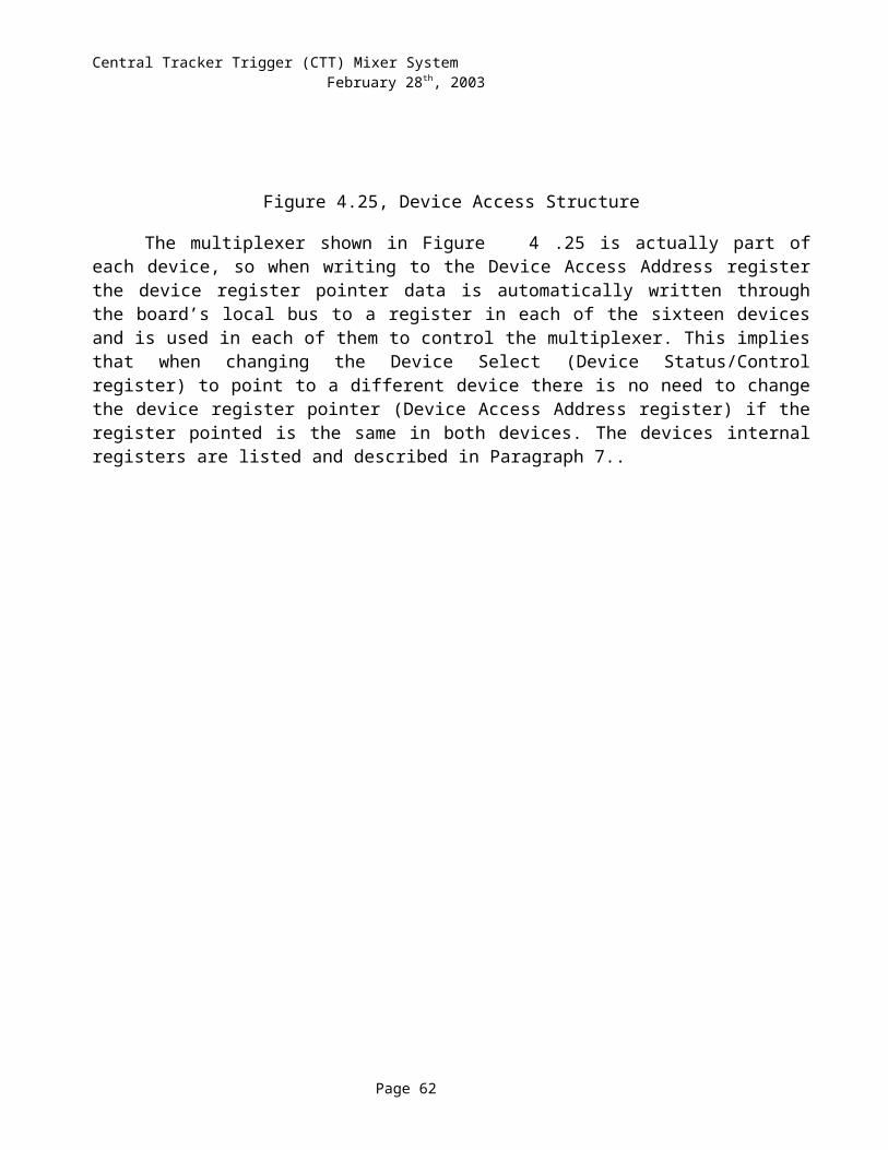
Central Tracker Trigger (CTT) Mixer System February 28th, 2003
The following tables describe the sixteen available sets of signals (or monitoring modes).
LED#Led Use. This set is used to monitor the input links clocks and DLLs.Link clock: Green LED ON if clock present, clock frequency is 45MHz < f < 55MHz and clock DLL is locked.Red LED-ON otherwise.
15..0 Link #15 to Link#0 clock status.
Table 6.34, LED's set #0 (input links clock and DLLs status).
LED#Led Use. This set is used to monitor the SYNC bit (data frame synchronization bit located on the LSb of each LVDS link). The link's own clock is used as timing reference. Green LED ON only if the SYNC bit is present and is respecting the protocol (one and only one high bit every seven clock cycles). Red LED ON otherwise.
15..0 Link #15 to Link#0 sync bit status.
Table 6.2, LED's set #1 (input links SYNC bit status).
LED#Led Use. This set is used to check the presence on the input links of a walking one test pattern. The pattern is specified in Paragraph 11. The link's own clock is used as timing reference. Green LED ON if the walking one pattern is detected, Red LED ON otherwise.
15..0 Link #15 to Link#0 walking one test pattern presence.
Table 6.35, LED's set #2 (input links Walking 1 test pattern detection).
LED#Led Use. This set is used to check the presence on the input links of a walking zero test pattern. The pattern is specified in Paragraph 11. The link's own clock is used as timing reference. Green LED ON if the walking zero pattern is detected, Red LED ON otherwise.
15..0 Link #15 to Link#0 walking zero test pattern presence.
Table 6.36, LED's set #3 (input links Walking 0 test pattern detection).
LED#Led Use. This set is used to monitor the SYNC bit (data frame synchronization bit located on the LSb of each LVDS link) after the synchronization process. The Global Clock is used as timing reference. Green LED ON only if the SYNC bit is present and is respecting the protocol (one and only one high bit every seven clock cycles). Red LED ON otherwise.
15..0 Link #15 to Link#0 sync bit status after synchronization.
Table 6.2, LED's set #4 (input links SYNC bit status after synchronization).
LED#
Led Use. This set is used to monitor the synchronization of the input links frames with the global sync. A link data frame is considered synchronized when the SYNC bit is in received in the same frame time slot as the SYNC bit used as timing reference (usually the SYNC received on link#0 of Mixer board #1).Green LED ON if link data frames are synchronized, Red LED ON otherwise.
15..0 Link #15 to Link#0 synchronization status.
Table 6.37, LED's set #5 (input links frame synchronization status).
Page 62

Central Tracker Trigger (CTT) Mixer System February 28th, 2003
LED#
Link #0 Output links Test Pattern detection. It is used to test the mixer output link when they are sending the test pattern. The test pattern transmission can be enabled through the Output Links Test Mode registers. The output links test pattern is specified in Paragraph 11. A 28 bit type LVDS cable should be used to loop-back one of the output links to the link#0 input link. Green LED ON if the pattern is detected, Red LED ON otherwise.
0 pattern detection.
1..15 not used, always OFF.
Table 6.38, LED's set #6 (Output links test pattern detection).
LED#
Input links control bits stream monitoring. Each LED is driven by the sequence of seven data bits received on a particular link. If a LED is red it means that the control bits on that link are always high ('1'), if the LED is green the control bits are always low ('0'). If the LED is orange it means that on that link some control bits are high and same are low or that at least one control bit is changing status. By default all the control bits are monitored, but a mask can be set in the "Monitoring Mode 7 Mask registers" (See 7.1.12) to monitor only a subset of control bits.
15..0 Link #15 to Link #0 control bits stream.
Table 6.39, LED's set #7 (Input links control bits stream monitoring).
LED#
Mixer Board local bus monitoring. This set is used to monitor the local bus data, address and control signals. When FPGAs device access operations are enabled (see Paragraph for an example) this monitoring mode can be used to view the content of FPGA's internal registers directly on the front panel LEDs. This is because when device access is enabled the local bus is driven with the content of FPGAs internal registers.
0 Local Data Bus bit 0 (FDAT0).
1 Local Data Bus bit 1 (FDAT1).
2 Local Data Bus bit 2 (FDAT2).
3 Local Data Bus bit 3 (FDAT3).
4 Local Data Bus bit 4 (FDAT4).
5 Local Data Bus bit 5 (FDAT5).
6 Local Data Bus bit 6 (FDAT6).
7 Local Data Bus bit 7 (FDAT7).
8 Local Data Bus read/write (/WRITE).
9 Local Bus Address Strobe (ASTRB) and FPGAs /INIT.
10 Local Bus Data Strobe (DSTRB).
11 FPGAs /PROGRAM (/PROGRAM).
12 FPGAs Configuration Clock (CONFIGCLK), green LED ON if clock is present, red LED ON if is absent.
13 Local Bus Transceiver enable (/CONFIGDAT_EN).
14 Local Bus Transceiver direction (/CONFIGDAT_DIR). '1' FPGAs to Board Controller, '0' Board Controller to FPGAs.
15 FPGA Global Clock (FPGACLK10), green LED ON if clock is present, red LED ON if is absent.
Table 6.40, LED's set #8 (Mixer Board local bus monitoring).
Page 63

Central Tracker Trigger (CTT) Mixer System February 28th, 2003
LED#Backplane serial bus and A16:D8 control signals monitoring. This set is used to monitor the A16:D8 general purpose bus control signals and the slow monitoring serial bus part of the backplane interfaces between the Mixer Board and the subrack controller.
0 SYSCLOCK (green LED ON if clock is present, red LED if clock is absent).
1 Address STRoBe (AS).
2 WRITE (WRITE).
3 Data Transfer ACKnoledge (/DTACK).
4 Bus ERRor (/BERR).
5 SYSRESET (SYSRST).
6 Transceivers enable (/VDAT_EN).
7 Transceiver direction (VDAT_DIR).
8 Serial Link Reset (STAT_RST).
9 Serial Link Clock (STAT_CLK), green LED ON if clock is present, red LED if clock absent.
10 Serial Link Data (STAT_DAT[n]).
11 Broadcast addressing.
12 Not Standard Mode (from Slow Monitoring register).
13 Input Links Error (from Slow Monitoring register)
14 Global Clock/SYNC Error (from Board Status/Control register)
15 Global Clock/SYNC Error history (from Board Status/Control register)
Table 6.41, LED's set #9 (Backplane serial bus and A16:D8 bus control signals monitoring).
LED# Led Use. This set is used to monitor the backplane address bus part of the A16:D8 general purpose bus interface between the Mixer Board and the subrack controller.
0..15 Address bit 0 (BADDR0) to Address bit 15 (BADDR15).
Table 6.5, LED's set #10 (Backplane A16:D8 general purpose bus address signals monitoring).
Page 64

Central Tracker Trigger (CTT) Mixer System February 28th, 2003
LED# This set is used to monitor the backplane data and geographical address signals part of the A16:D8 general purpose bus interface between the Mixer Board and the subrack controller.
0 Data bit 0 (BDAT0).
1 Data bit 1 (BDAT1).
2 Data bit 2 (BDAT2).
3 Data bit 3 (BDAT3).
4 Data bit 4 (BDAT4).
5 Data bit 5 (BDAT5).
6 Data bit 6 (BDAT6).
7 Data bit 7 (BDAT7).
8 Slot Address bit 0 (MOD_ID0).
9 Slot Address bit 1 (MOD_ID1).
10 Slot Address bit 2 (MOD_ID2).
11 Slot Address bit 3 (MOD_ID3).
12 Slot Address bit 4 (MOD_ID4).
13 Not used, always OFF.
14 Not used, always OFF.
15 Not used, always OFF.
Table 6.5, LED's set #11 (A16:D8 general purpose bus data and slot address signals monitoring).
LED#
This set is used to verify the configuration of 16 of the 17 FPGAs of a Mixer Board. The only FPGA not considered is the Board Controller which is automatically configured at power-up by an EPROM.Green: FPGA configured correctly. Red: FPGA not configured. The name in parenthesis is the one used on the board electrical schematic.
0 Configuration Done BE DFE1 Yellow-Purple FPGA (DONE11).
1 Configuration Done BE DFE1 Red-Blue FPGA (DONE12).
2 Configuration Done BE DFE1 Orange-Green FPGA (DONE13).
3 Configuration Done BE DFE0 Red-Blue FPGA (DONE14).
4 Configuration Done BE DFE0 Orange-Green FPGA (DONE15).
5 Configuration Done BE DFE0 Yellow-Purple FPGA (DONE16).
6 Configuration Done FE LinkIn13..15 FPGA (DONE1).
7 Configuration Done FE LinkIn4..6 FPGA (DONE2).
8 Configuration Done FE LinkIn1..3 FPGA (DONE3).
9 Configuration Done FE LinkIn10..12 FPGA (DONE4).
10 Configuration Done FE LinkIn0 FPGA (DONE5).
11 Configuration Done Backplane Left Driver FPGA (DONE6).
12 Configuration Done FE LinkIn7..9 FPGA (DONE7).
13 Configuration Done Backplane DFE0 Receiver FPGA (DONE8).
14 Configuration Done Backplane DFE1 Receiver FPGA (DONE9).
15 Configuration Done Backplane Right Driver FPGA (DONE10).
Table 6.6, LED's set #12 (Default mode, FPGA configuration status).Page 65

Central Tracker Trigger (CTT) Mixer System February 28th, 2003
LED# Output Links Test Mode Enable status.
0 DFE 0 Green Link (00) status.
1 DFE 0 Green Link (01) status.
2 DFE 0 Orange Link (02) status.
3 DFE 0 Purple Link (03) status.
4 DFE 0 Yellow Link (04) status.
5 DFE 0 Blue Link (05) status.
6 DFE 0 Red Link (06) status.
7 DFE 0 Red Link (07) status.
8 DFE 1 Green Link (10) status.
9 DFE 1 Green Link (11) status.
10 DFE 1 Orange Link (12) status.
11 DFE 1 Purple Link (13) status.
12 DFE 1 Yellow Link (14) status.
13 DFE 1 Blue Link (15) status.
14 DFE 1 Red Link (16) status.
15 DFE 1 Red Link (17) status.
Table 6.7, LED's set #13 (Output Links Test Mode Enable status).
LED# Input Links Error Status. This set is used to monitor the input links status using the same signals driving Input Links Error Status registers (0x05, 0x06).
15..0 Status of the input links #15 (bit 15) to #0 (bit 0). A high value ('1', red LED ON) indicates that the corresponding input link has one of the following critical errors:
1) Link clock: missing or out of frequency range (45MHZ to 55MHz) or Delay Locked Loop not locked;
2) Link frame marker (SYNC) before synchronization: missing or not respecting the protocol (one and only one high bit every seven clock cycles);
5) Link frame marker (SYNC) after synchronization: missing or not respecting the protocol (one and only one high bit every seven clock cycles);
6) Link frame synchronization: the frames are not synchronized with those of the reference link (usually link#0 on the first board (master) in the mixer subsystem (group of four boards handling the data from one supersector)).
Table 6.7, LED's set #14 .(Input Links Error Status).
LED# Led Test. This set is used to check that all the LEDs are functioning.
15..0 Both Green and Red LEDs are always ON (Orange light).
Table 6.7, LED's set #15 (LED Test).
Page 66

Central Tracker Trigger (CTT) Mixer System February 28th, 2003
7. Appendix A – Devices registers
The board controller internal registers allow for most of the user controls needed during normal system operations. Beside the board controller there are sixteen FPGAs on a mixer board and each one has internal registers. These registers allow access to advanced features generally used for diagnostic purposes during system debugging, testing and commissioning. These features can also be utilized periodically to test system operations or in the event of a malfunction.
7.1 FrontEnd Devices
Table 7.42 lists the internal registers of the six front-end FPGAs. The address specified in the first column refers to the FPGA internal address and is the one to be used in the Device Access Address register. Please refer to Paragraph 4.5.12 for more information on the Device Access Structure. The table is followed by a description of each of the registers.
Register address
Register name and use.
IN0[Dev# 1010b]
IN1..3[Dev# 1000b]
IN4..6[Dev# 0111b]
IN7..9[Dev# 1100b]
IN10..12[Dev# 1001b]
IN13..15[Dev# 0110b]
0x00 Device Firmware X X X X X X
0x01 Link pointer X -- -- -- -- --
0x02..0x0F -- -- -- -- -- -- --
0x10 Link Status A (Read-Only) Link#0 Link#1 Link#4 Link#7 Link#10 Link#13
0x11 Link Status B (Read-Only) Link#0 Link#1 Link#4 Link#7 Link#10 Link#13
0x12 Link Control (Read/Write) Link#0 Link#1 Link#4 Link#7 Link#10 Link#13
0x13 Frame Sync Status (Read-Only) Link#0 Link#1 Link#4 Link#7 Link#10 Link#13
0x14 Frame Sync Status History (Read-Only) Link#0 Link#1 Link#4 Link#7 Link#10 Link#13
0x15 Monitoring Mode 7 Mask Link#0 Link#1 Link#4 Link#7 Link#10 Link#13
0x16 Link Control Bits Status Link#0 Link#1 Link#4 Link#7 Link#10 Link#13
0x17..0x1F -- -- -- -- -- -- --
0x20 Link Status A (ReadOnly) -- Link#2 Link#5 Link#8 Link#11 Link#14
0x21 Link Status B (ReadOnly) -- Link#2 Link#5 Link#8 Link#11 Link#14
0x22 Link Control (Read/Write) -- Link#2 Link#5 Link#8 Link#11 Link#14
0x23 Frame Sync Status (Read-Only) -- Link#2 Link#5 Link#8 Link#11 Link#14
0x24 Frame Sync Status History (Read-Only) -- Link#2 Link#5 Link#8 Link#11 Link#14
0x25 Monitoring Mode 7 Mask -- Link#2 Link#5 Link#8 Link#11 Link#14
0x26 Link Control Bits Status -- Link#2 Link#5 Link#8 Link#11 Link#14
0x27..0x2F -- -- -- -- -- -- --
0x30 Link Status A (Read-Only) -- Link#3 Link#6 Link#9 Link#12 Link#15
0x31 Link Status B (Read-Only) -- Link#3 Link#6 Link#9 Link#12 Link#15
0x32 Link Control (Read/Write) -- Link#3 Link#6 Link#9 Link#12 Link#15
Page 67

Central Tracker Trigger (CTT) Mixer System February 28th, 2003
0x33 Frame Sync Status (Read-Only) -- Link#3 Link#6 Link#9 Link#12 Link#15
0x34 Frame Sync Status History (Read-Only) -- Link#3 Link#6 Link#9 Link#12 Link#15
0x35 Monitoring Mode 7 Mask -- Link#3 Link#6 Link#9 Link#12 Link#15
0x36 Link Control Bits Status -- Link#3 Link#6 Link#9 Link#12 Link#15
0x37..0x3F -- -- -- -- -- -- --
0x40 Control bits masking Link#0 -- -- -- -- --
0x41 Control bits masking Link#1 -- -- -- -- --
0x42 Control bits masking Link#2 -- -- -- -- --
0x43 Control bits masking Link#3 -- -- -- -- --
0x44 Control bits masking Link#4 -- -- -- -- --
0x45 Control bits masking Link#5 -- -- -- -- --
0x46 Control bits masking Link#6 -- -- -- -- --
0x47 Control bits masking Link#7 -- -- -- -- --
0x48 Control bits masking Link#8 -- -- -- -- --
0x49 Control bits masking Link#9 -- -- -- -- --
0x4A Control bits masking Link#10 -- -- -- -- --
0x4B Control bits masking Link#11 -- -- -- -- --
0x4C Control bits masking Link#12 -- -- -- -- --
0x4D Control bits masking Link#13 -- -- -- -- --
0x4E Control bits masking Link#14 -- -- -- -- --
0x4F Control bits masking Link#15 -- -- -- -- --
0x50 Input Links Control bits status at Link0 FPGA Link#15..0 -- -- -- -- --
0x51 EC bits status X -- -- -- -- --
0x52 ECS bits status X -- -- -- -- --
0x53..0xFF -- -- -- -- -- -- --
Table 7.42, Front-End devices registers.
Page 68

| 7 6 5 4 | 3 2 1 0 |
D e v ic e F irm w a re R e g is te r (R E A D O N LY )
D E V IC E ID d ev ice # | d e v ice # b in a ry | d e v ice n am e: 0 0000 1 0001 2 0010 3 0011 4 0100 5 0101 6 0110 7 0111 8 1000 9 1
FPGA DFE1 Yellow-PurpleFPGA DFE1 Blue-RedFPGA DFE1 Green-OrangeFPGA DFE0 Blue-RedFPGA DFE0 Green-Orange FPGA DFE0 Yellow-PurpleFPGA IN 13..15FPGA IN 4..6FPGA IN 1..3
001 FPGA IN 10..12 10 1010 FPGA IN 0 11 1011 FPGA Backplane Left Driver 12 1100 FPGA IN 7..9 13 1101 FPGA Backplane DFE0 Receiver 14 1110 FPGA Backplane DFE1 Receiver 15 1111 FPGA Backplane Right Driver
Virte x
S p a rtan X L
M ix e r B o a rd #0 0 M ixe r B o a rd 1 , s lo ts : 2 , 6 , 1 0 , 1 4 , 1 8 . 0 1 M ixe r B o a rd 2 , s lo ts : 3 , 7 , 11 , 1 5 , 1 9 .1 0 M ixe r B o a rd 3 , s lo ts : 4 , 8 , 1 2 , 1 6 , 2 0 .11 M ix er B o a rd 4 , s lo ts : 5 , 9 , 1 3 , 1 7 , 2 1 .
XX
Central Tracker Trigger (CTT) Mixer System February 28th, 2003
7.1.1 Device Firmware Register
This register contains information about the FPGA/device accessed. It allows verifying which device is being accessed.
Figure 7.36, Device Firmware register.
7.1.2 Link pointer register
Allows selecting which link is to be monitored by some of the diagnostic. The diagnostic information can be read back through FPGA's internal registers. The content of these registers depends on the link pointed to by the "Link Pointer register". The four bits used as link pointer represent the link# in hexadecimal.
Figure 7.37, Link Pointer register
Currently only the "Input Links Control bits status at IN0 FPGA" register needs the Link pointer register.
Page 69
| 7 6 5 4 | 3 2 1 0 |
L in k P o in te r R eg iste r (R E A D /W R IT E )
L in k P o in te r
X XX X

| 7 6 5 4 | 3 2 1 0 |
In p u t L in k S ta tu s R eg is te r A (R E A D O N LY )
C loc k E rro rS y n c E rro r
F ra m e S y n ch ro n iza tio n E rro rC loc k E rro r H is to ry S y n c E rro r H isto ry
F ra m e S y n ch ro n iza tio n E rro r H is to ry
S y n c E rro r (a f te r sy n c h ro n iza tio n )
S y n c E rro r (a f te r sy n c h ro n iza tio n ) H is to ry
Central Tracker Trigger (CTT) Mixer System February 28th, 2003
7.1.3 Input Link Status registers
Figure 7.38, Input Link Status register.
7.1.4 Input Link Control register
Figure 7.39, Input Link Control register
Figure 7.40, Data synchronization and link controls.
Page 70
| 7 6 5 4 | 3 2 1 0 |
In p u t L in k S ta tu s R eg is te r B (R E A D O N LY )
W alk in g ze ro p a tte rn d e tec tio nW a lk in g o n e p a tte rn d e tec tio nO u tp u t lin k s test p a tte rn d e tec tio nX
X
W a lk in g z e ro p a tte rn d e tec tio n h is to ryW alk in g o n e p a tte rn d e tec tio n h is to ryO u tp u t l in k s tes t p a tte rn d e te c tio n h is to ry
D ataS y n ch ro n iza tio n
D Q D Q D Q
E d ge S E L
D Q
D Q D Q
K ill L in k D atato B ack E n d an d
B ack p lan e F P G A s
to L in k # 0 F P G A
D 0D 1D 2D 3
E 0
E 1
D e lay S E L
S Y N C d etec tio n (a fte r sy n ch ro n iza tio n )F ram e sy n ch ro n iza tio n d e tec tio nC o n tro l b its ex trac tion /d e tec tio nL in k F IF OC o n tro l b its lo g ic ( lin k # 0 O N LY )
S Y N C to C lo ck C o n tro lle r(L in k# 0 O N LY )
L in kS w apS E L
*( )
*( ) see A p p en d ix L
| 7 6 5 4 | 3 2 1 0 |
In pu t L in k C on tro l R eg is te r (R E A D /W R IT E )
R e se t H is to ry in fo rm a tio nK ill lin k d a taD ata sam p lin g ed g e se lec t0 E 01 E 1 (d e fau lt)
L o g ic A n a ly ze r Te st P O D co n fig (L in k # 0 O N LY ) 0 : 2 1 b its co n fig u ra tio n (d e fau lt) 1 : 2 8 b its co n fig u ra tio n .
D elay se lec t0 0 D 0 0 1 D 11 0 D 211 D 3
(d efau lt)
XX
Central Tracker Trigger (CTT) Mixer System February 28th, 2003
7.1.5 Frame Sync Status register
The frame synchronization register data is used to determine the link SYNC (link frame marker) position relative to the global SYNC. Its content is generated by sampling with the global SYNC signal the content of an 8bit long shift register fed by the link SYNC. When the data frames on a link are synchronized to the global SYNC all of the bits but the least and most significative will readback “0” (see Figure 7.42).
Figure 7.41, Frame Synchronization Status register.
Figure 7.42, Frame Synchronization Status register content.
Page 71
| 7 6 5 4 | 3 2 1 0 |
F ra m e S y nc h ro n iz a tio n S ta tu s R e g is te r (R E A D O N LY )
F ram e S Y N C D a ta
c urre n t d a ta fram e
D a ta F ra m e (7 tim e s lo ts)
p re v io u s d a ta fra m e n e x t d ata fra m e
L in k S Y N C
G lo b a l S Y N C
1 0 0 0 0 0 0 1
G lo b a l S Y N C
0 0 0 1 0 0 0 0D a ta F ram e 4 tick s e a rly o r 3 t ic k s la te
G lo ba l S Y N C
0 0 1 0 0 0 0 0
G lo b a l S Y N C
0 1 0 0 0 0 0 0
G lo b a l S Y N C
0 0 0 0 0 0 1 0
G lo b a l S Y N C
0 0 0 0 0 1 0 0
0 0 0 0 1 0 0 0
G lo b a l S Y N C
0 0 0 1 0 0 0 0
D a ta F ram e 5 tick s e a rly o r 2 tic k s la te
D a ta F ram e 6 tic k s e a rly o r 1 tick la te
D a ta F ram e sy n ch ro n ize d
D a ta F ram e 1 tic k ea rly o r 6 tic ks la te
D a ta F ram e 2 tic k s ea rly o r 5 tic k s la te
D a ta F ram e 3 tic k s ea rly o r 4 tic k s la te
D a ta F ram e 4 tic k s ea rly o r 3 tic k s la te
G lo b a l S Y N C

Central Tracker Trigger (CTT) Mixer System February 28th, 2003
7.1.6 Frame Sync Status History register
The Frame Sync Status History register is used to keep track of the changes in the Frame Sync Status register. The register content is zero at power up or reset (or with the "reset history information" from Input Link Control register) and each of is bit is set and remain set to '1' if the corresponding bit in the Frame Sync Status register is '1'.
Figure 7.43, Frame Synchronization Status History register.
7.1.7 Input Link Control Bits Mask register
Each input link is preset to receive one control bit at each time slot embedded in the 7-time slot data stream, for a total of 7 control bits per link. The control bits from every link are sent to one FPGA (the Link#0 FPGA) where, at each time slot, they are all ORed and XORed to generate the Embedded Command (EC) and the Embedded Command Status (ECS) bit. The EC and ECS bits are then sent to the backend FPGAs to be embedded in some of the output data streams.
If any of the control bits are not sent by the front end electronics (AFEs) to the mixer, the missing control bits need to be masked on the Mixer boards in order to perform the OR and XOR operation only on the valid control bits. This masking is done in the Link#0 FPGA before the OR and XOR operation are performed. To allow this, there are 16 "input link control bits mask registers" for each input link on a mixer board. If any control bit needs to be masked, the corresponding bit in the masking register should be set to '0'. The default content of each of these registers is 0x01 for link#0 and 0xFF for all the other links. The reason for having all the control bits masked on input link#0 is that the data mapping done by the AFEs driving link#0 doesn't comply with the mixer design specification so the control bits aren't where the mixer would expect them.
Figure 7.44, Input Link Control Bits Mask register.
Page 72
| 7 6 5 4 | 3 2 1 0 |
F ram e S y n ch ro n iz a tio n S ta tu s H is to ry R eg is te r (R E A D O N LY )
F ra m e S Y N C H is to ry D a ta
| 7 6 5 4 | 3 2 1 0 |
In pu t L ink C o n tro l B its M ask R e g is te r (R E A D /W R IT E )
E n ab le m ask in g
Tim e s lo t 2 m ask in g
Tim e s lo t 4 m ask in gTim e s lo t 5 m ask in gTim e s lo t 6 m ask in g
Tim e s lo t 3 m ask in g
Tim e s lo t 7 m ask in g

Central Tracker Trigger (CTT) Mixer System February 28th, 2003
7.1.8 Input Link Control Bits Status registers
Allows verifying of the presence of control bits on each of the sixteen input links. There is one of these registers for each input link.
The registers content reflects the control bits received on each link and is not affected by any control bits mask selection made in the "Input Link Control Bits Mask register".
Figure 7.45, Input Link Control Bits Status register
7.1.9 Input Link Control Bits Status at Link#0 FPGA register
Allows verifying of the presence of control bits from each of the sixteen input links at the Link#0 FPGA, which is the place where the control bits are combined to generate the Embedded Command and Embedded Command Status bits for the output data stream.
Only one link at a time can be monitored. The link to be monitored is selected in the "Link Pointer register" inside the IN0 FPGA (device# 0x0A). The register content reflects the control bits received on each link and is not affected by any control bits mask selection made in the "Input Link Control Bits Mask register". The register is NOT reset when the monitored link is changed. Because of this, after a link change and when the latching option (bit#0) is used there is the need to disable and re-enable it in order for the register to show the correct information.
This register will be probably removed in future firmware upgrades.
Figure 7.46, Input Link Control Bits Status register
Page 73
| 7 6 5 4 | 3 2 1 0 |
In p u t L ink s C o n tro l B its S ta tu s a t L ink # 0 F P G A R e g is te r (R E A D /W R IT E )
E n ab le la tch in g (R ead /W rite )
T im e slo t 2
Tim e slo t 4Tim e s lo t 5Tim e s lo t 6
Tim e slo t 3
Tim e s lo t 7
(R ead O n ly )
| 7 6 5 4 | 3 2 1 0 |
In p u t L in k s C o n tro l B its S tatu s R eg is te r (R E A D /W R IT E )
E n ab le la tch in g (R e ad /W rite )
T im e s lo t 2
T im e s lo t 4T im e s lo t 5T im e s lo t 6
Tim e s lo t 3
T im e s lo t 7
(R ea d O n ly )

Central Tracker Trigger (CTT) Mixer System February 28th, 2003
7.1.10 Embedded Command Bits status register
Allows verifying of the presence of the Embedded Command bits generated ORing the control bits received from the 16 input links.
Figure 7.47, Embedded Command Bits Status Register.
7.1.11 Embedded Command Status Bits status register
Allows verifying of the presence of the Embedded Command Status bits generated XORing the control bits received from the 16 input links.
Figure 7.48, Embedded Command Status Bits Status Register.
Page 74
| 7 6 5 4 | 3 2 1 0 |
E m b e d d e d C o m m a n d B its S ta tu s R e g is te r (R E A D /W R IT E )
E n ab le la tch in g (R e ad /W rite )
T im e s lo t 2
Tim e slo t 4Tim e s lo t 5Tim e s lo t 6
Tim e s lo t 3
Tim e s lo t 7
(R ea d O n ly )
| 7 6 5 4 | 3 2 1 0 |
E m b edd ed C om m an d S ta tu s B its S ta tu s R eg is te r (R E A D /W R IT E )
E n ab le la tch in g (R ead /W rite )
Tim e s lo t 2
Tim e slo t 4Tim e s lo t 5Tim e s lo t 6
Tim e s lo t 3
Tim e s lo t 7
(R ead O n ly )

Central Tracker Trigger (CTT) Mixer System February 28th, 2003
7.1.12 Monitoring Mode 7 Mask register
Each input link is preset to receive one control bit at each time slot embedded in the 7-time slot data stream, for a total of 7 control bits per link. LED monitoring mode 7 (see Paragraph 6.1) allows seeing on the front panel LEDs the presence of the control bits data stream. The Monitoring Mode 7 Mask register allows individual masking on any input link for any set of control bits in order to have monitoring mode 7 shows the presence of a desidered control bits subset. There are 16 "input link control bits mask registers", one for each input link on a mixer board. The default content of each of these registers is 0xFF. If any control bit needs to be masked, the corresponding bit in the masking register should be set to '0'.
Figure 7.49, Monitoring Mode 7 Mask register.
Page 75
| 7 6 5 4 | 3 2 1 0 |
M on ito rin g M o de 7 M a sk R e g is te r (R E A D /W R IT E )
E n ab le m ask in g
Tim e s lo t 2 m ask in g
Tim e s lo t 4 m a sk in gTim e s lo t 5 m ask in gTim e s lo t 6 m ask in g
Tim e s lo t 3 m ask in g
Tim e s lo t 7 m ask in g

Central Tracker Trigger (CTT) Mixer System February 28th, 2003
7.2 Backplane Devices
Partially Implemented
Grayed blocks are not implemented.Register address
Register name and use.
DFE0_RX[Dev# 1101b]
DFE1_RX[Dev# 1110b]
LEFT_DRV[Dev# 1011b]
RIGHT_DRV[Dev# 1111b]
0x00 Device Firmware X X X X
0x01 -- -- -- --
0x02 Device Control X X X X
0x03..0x6F -- -- -- -- --
0x70 Clock DLL Error (Read-Only)
-- -- -- X
0x71 Clock Frequency Error (Read-Only)
-- -- -- X
0x72 SYNC Error (Read Only)
-- -- -- X
0x73 Clock/SYNC Select Status (Read Only)
-- -- -- X
0x74..0x7F -- -- -- -- --
0x80 Backplane Driver Status
(Read-Only)
-- -- X X
0x81 Backplane Driver Control
(Read/Write)
-- -- X X
0x82..0x8F -- -- -- -- --
0x90 Backplane Receiver Status
(Read-Only)
X X -- --
0x91 Backplane Receiver Control
(Read/Write)
X X -- --
0x92..0xFF -- -- -- -- --
Table 7.43, Backplane Devices registers.
Page 76

Central Tracker Trigger (CTT) Mixer System February 28th, 2003
7.2.1 Device Firmware Register
See paragraph 7.1.1.
7.2.2 Device Control register
Figure 7.50, Device Control register
7.2.3 Clock DLL Error register
Figure 7.51, Clock DLL Error register.
7.2.4 Clock Frequency Error register
Figure 7.52, Clock Frequency Error register.
Page 77
| 7 6 5 4 | 3 2 1 0 |
C lo c k D L L E rro r R eg is te r (R E A D O N LY )
L o ca l C lo ck D L L E rro rL in k # 0 C lo ck D L L E rro rB ack p lan e C lo ck D L L E rro rG lo b a l C lo c k D L L E rro rL o ca l C lo ck D L L E rro r h isto ryL in k # 0 C lo ck D L L E rro r h is to ryB a ck p lan e C lo ck D L L E rro r h isto ryG lo b a l C lo ck D L L E rro r h is to ry
| 7 6 5 4 | 3 2 1 0 |
C lo c k D L L E rro r R eg is te r (R E A D O N LY )
XL in k # 0 C lo ck F req u en cy E rro rB a ck p lan e C lo ck F req u en cy E rro rG lo b a l C lo ck F req u en c y E rro rXL in k # 0 C lo ck F req u en cy E rro r h isto ryB ack p lan e C lo ck F req u en cy E rro r h is to ryG lo b a l C lo c k F req u en cy E rro r h is to ry
| 7 6 5 4 | 3 2 1 0 |
D ev ic e C o n tro l R e g iste r (R e ad /W rite )
R e se t h is to ry in fo rm atio nXXXXXXX

Central Tracker Trigger (CTT) Mixer System February 28th, 2003
7.2.5 SYNC Error register
Figure 7.53, SYNC Error register
7.2.6 Clock/SYNC Select Status register
Figure 7.54, Clock/SYNC Select Status register
Page 78
| 7 6 5 4 | 3 2 1 0 |
C lo ck /S Y N C S e le c t S ta tu s R eg is te r (R E A D O N LY )
L o cal C lo c k /S Y N C E n ab leL in k # 0 C lo ck /S Y N C E n ab leB ack p lan e C lo ck /S Y N C E n ab leG N D C lo ck /S Y N C E n ab leL o c a l C lo ck /S Y N C E n ab le h isto ryL in k # 0 C lo ck /S Y N C E n ab le h is to ryB ack p lan e C lo ck /S Y N C E n ab le h is to ryG N D C lo c k /S Y N C E n ab le h is to ry
| 7 6 5 4 | 3 2 1 0 |
S Y N C E rro r R e g is te r (R E A D O N LY )
L o cal S Y N C E rro rL in k # 0 S Y N C E rro rB ack p lan e S Y N C E rro rG lo b a l S Y N C E rro rL o ca l S Y N C E rro r h is to ryL in k # 0 S Y N C E rro r h is to ryB a ck p lan e S Y N C E rro r h is to ryG lo b a l S Y N C E rro r h is to ry

Central Tracker Trigger (CTT) Mixer System February 28th, 2003
7.2.7 Backplane Driver Status register
NOT IMPLEMENTED
7.2.8 Backplane Driver Control register
NOT IMPLEMENTED
7.2.9 Backplane Receiver Status register
NOT IMPLEMENTED
7.2.10 Backplane Receiver Control register
NOT IMPLEMENTED
Page 79

Central Tracker Trigger (CTT) Mixer System February 28th, 2003
7.3 BackEnd Devices
Partially implemented, grayed blocks are not implemented.
Register address
Register name and use.
DFE0_GO[Dev# 0100b]
DFE0_YP[Dev# 0101b]
DFE0_BR[Dev# 0011b]
DFE1_GO[Dev# 0010b]
DFE1_YP[Dev# 0000b]
DFE1_BR[Dev# 0001b]
0x00 Device Firmware X X X X X X
0x01 -- -- -- -- -- -- --
0x02 Device Control X X X X X X
0x03..0x0F -- -- -- -- -- -- --
0x10..0x9F -- -- -- -- -- -- --
0xA0 Link Status Green (00, 01) Yellow (04) Blue (05) Green (10, 11) Yellow (14) Blue (15)
0xA1 Link Control Green (00, 01) Yellow (04) Blue (05) Green (10, 11) Yellow (14) Blue (15)
0xA2Embedded
Command Bits mask
-- -- X -- -- X
0xA3..0xAC -- -- -- -- -- -- --
0xAD Link FIFO Memory Pointer
Green (00, 01) Yellow (04) Blue (05) Green (10, 11) Yellow (14) Blue (15)
0xAE Link FIFO Control Green (00, 01) Yellow (04) Blue (05) Green (10, 11) Yellow (14) Blue (15)
0xAF Link FIFO Access Green (00, 01) Yellow (04) Blue (05) Green (10, 11) Yellow (14) Blue (15)
0xB0 Link Status Orange (02) Purple (03) Red (06, 07) Orange (12) Purple (13) Red (16, 17)
0xB1 Link Control Orange (02) Purple (03) Red (06, 07) Orange (12) Purple (13) Red (16, 17)
0xB2Embedded
Command Bits mask
X -- -- X -- --
0xB3..0xBC -- -- -- -- -- -- --
0xBD Link FIFO Memory Pointer
Orange (02) Purple (03) Red (06, 07) Orange (12) Purple (13) Red (16, 17)
0xBE Link FIFO Control Orange (02) Purple (03) Red (06, 07) Orange (12) Purple (13) Red (16, 17)
0xBF Link FIFO Data Orange (02) Purple (03) Red (06, 07) Orange (12) Purple (13) Red (16, 17)
0xC0..0xFF -- -- -- -- -- -- --
Table 7.44, BackEnd Devices registers.
7.3.1 Device Firmware Register
See paragraph 7.1.1.
7.3.2 Device Control Register
See paragraph 7.2.2.
Page 80

| 7 6 5 4 | 3 2 1 0 |
E m b edd ed C o m m an d B its M a sk R eg is te r (R E A D /W R IT E )
E n ab le m ask in g
Tim e slo t 2 m ask in g
Tim e s lo t 4 m ask in gTim e slo t 5 m ask in gTim e slo t 6 m ask in g
Tim e slo t 3 m ask in g
Tim e slo t 7 m ask in g
Central Tracker Trigger (CTT) Mixer System February 28th, 2003
7.3.3 Output Link Status register
NOT IMPLEMENTED
7.3.4 Output Link Control register
This register allows to shutdown the output link data stream and the output link SYNC bit. Some of the output links are used to transmit the Embedded Command and the Embedded Command Status bits (or control bits). These bits are not affected by the data stream shutdown, if desired they can be masked using the Embedded Command Bits Mask register.
Figure 7.55, Link Control register
7.3.5 Output Link Embedded Command Bits Mask register
This register allows masking the control bits on the output links. Only 4 output links are carrying control bits, these are the orange (02, 12) and the blue (05, 15) links. The control bits can be masked independently on each of these links. The masking affects both the Embedded Command Bits (ECB) and the Embedded Command Status Bits (ECSB).
Figure 7.56, Embedded Command Bits Mask register.
Page 81
| 7 6 5 4 | 3 2 1 0 |
L in k C on tro l R e g is te r (R e ad /W rite )
D ata S tream S h u td o w n
XXXXXX
S Y N C S h u td o w n

Central Tracker Trigger (CTT) Mixer System February 28th, 2003
7.3.6 Output Link FIFO
Each output link has a 32 bit wide FIFO that can be used to sample the data stream sent to the output link transmitters or to feed the output link transmitters with fake events to test the system downstream.
Figure 7.57, Output Link FIFO
Figure 7.58, Output Link FIFO Access/Control Structure
Page 82
b y te (0 ,0 )
D ata rece iv ed fro m A F E a n d re o rg a n ize d b y tr igg e r se c to rs
D ata to O u tp u t L ink s Tra n sm itte rsX
O u tpu t L in k F IF O
| 7 6 5 4 | 3 2 1 0 | |1 5 1 4 1 3 1 2 | 11 1 0 9 8 | |2 3 2 2 2 1 2 0 |1 9 1 8 1 7 1 6 |
| 7 6 5 4 | 3 2 1 0 | |1 5 1 4 1 3 1 2 | 11 1 0 9 8 | |2 3 2 2 2 1 2 0 |1 9 1 8 1 7 1 6 |
|3 1 3 0 2 9 2 8 |2 7 2 6 2 5 2 4 |
|3 1 3 0 2 9 2 8 |2 7 2 6 2 5 2 4 |
X
b y te (1 ,0 )b y te (2 ,0 )b y te (3 ,0 )
b y te (0 ,1 2 )
b y te (0 ,1 3 )b y te (1 ,1 3 )b y te (2 ,1 3 )by te (3 ,13 )
by te (3 ,12 ) b y te (2 ,1 2 ) b y te (1 ,1 2 )
F IF O in R x M o d e
b y te (0 ,6 )b y te (1 ,6 )b y te (2 ,6 )b y te (3 ,6 )
E v en t #0
E v en t #1
F IF O in T x M o d e
co lu m n # 0co lu m n # 1co lu m n # 2co lum n #3
ro w # 0
ro w # 7
ro w # 1 2
ro w # 1 3
| 7 6 5 4 | 3 2 1 0 |
O u tpu t L in k F IF O C o n tro l R eg is ter
| 7 6 5 4 | 3 2 1 0 |
O u tpu t L in k F IF O M em o ry P o in te r R eg is te r
| 7 6 5 4 | 3 2 1 0 |
O u tp u t L in k F IF O D ata A c cess R eg is te r
F IF O D a ta
S E L
(3 , 0 ) (2 , 0 ) (1 , 0 ) (0 , 0 )
(3 , 1 ) (2 , 1 ) (1 , 1 ) (0 , 1 )
(3 , 6 ) (2 , 6 ) (1 , 6 ) (0 , 6 )
(3 , 1 3 ) (2 , 1 3 ) (1 , 13 ) (0 , 1 3 )
(3 , 7 ) (2 , 7 ) (1 , 7 ) (0 , 7 )C o lum n , R o w 0 x 2 D
ev en t # 0
ev en t #1
O u tp u t L in k F IF O
| 7 6 5 4 | 3 2 1 0 |
F IF O Trigg er C on tro l R eg is te r (B o ard C o n tro lle r)

Central Tracker Trigger (CTT) Mixer System February 28th, 2003
The FIFO Trigger Control register is used to trigger the output links FIFOs. This register allows selecting the trigger duration from 0 (no trigger) to 15 data frames or a continuous trigger. The trigger duration (even the continuous trigger) will always be an entire number of frames and is automatically synchronized to the global SYNC (frame marker). The trigger operates simultaneously on all the FIFOs on a Mixer Board.
Each individual FIFO can be accessed in Read/Write using the thorough the FIFO Data Access register that connect to one of the 56 byte-wide memory locations of the FIFO. The location accessed is the one pointed by the FIFO Memory Pointer register.
The FIFO can be used to replace events in the output data stream with the FIFO content (transmit mode) or to store events from the output data stream in the FIFO (receive mode). The FIFO can operate in four different “FIFO Event Modes” which are used select the section of the FIFO to be used (event#0, event#1 or both) or to disable the FIFO.
The FIFO is by default in Transmit Mode and in FIFO Event Mode “01”. With these settings, when a trigger is generated (FIFO Trigger Control register), only event#0 will be transmitted for the duration of the trigger. When in transmit mode the FIFO content is set to replace completely the output data stream content including the SYNC and the control bits. The FIFO Control register provides the user with the option to do not disrupt the control bits flow with the FIFO content.
A board reset doesn’t affect the FIFO content.
The FIFO is not accessible when it is receiving a trigger signal.
7.3.7 Output Link FIFO Memory Pointer register
This register is used to select one of the 56 byte-wide locations of the FIFO. The location pointed by the register is accessible through the "Output Link FIFO Data Access register".
Figure 7.59, Output Link FIFO Memory Pointer register
Page 83
| 7 6 5 4 | 3 2 1 0 |
L in k F IF O M e m o ry P o in te r R e g is te r (R E A D /W R IT E )
R o w P o in te r
X X
C o lu m n P o in te r

Central Tracker Trigger (CTT) Mixer System February 28th, 2003
7.3.8 Output Link FIFO Control register
This register is used to control the FIFO behavior.
Figure 7.60, Output Link FIFO Control register
Bit# Name (Type) Interpretation
7..6 -- Not used.
5..4 FIFO Event Mode Select
The FIFO can operate in four event modes:“00”: FIFO disabled, the trigger is ignored.“01”: FIFO one event deep. Event #0 is used.“10”: FIFO one event deep. Event#1 is used.“11”: FIFO two event deep, both event #0 and #1 are used.
The event mode affect both the receive and transmit mode of operation.
3 -- Not used
2 FIFO Trigger Read Only. Is high when the FIFO is receiving a trigger signal from the board controller (FIFO Trigger Control register).
1 Control Bits Source Select
Some of the output links are used to transmit control bits together with the data stream. When the FIFO is operating in transmit mode and a trigger is received the content of the FIFO is used on the output link data stream and replace the data bits, the SYNC (frame marker) bit and the control bits. To avoid disrupting the control bit flow the Control Bits Source Select bit can be set high ‘1’.
0 Receive/Transmit Mode Select
Allow to select if the FIFO has to operate in Transmit (‘0’, default) or in Receive (‘1’) mode. The transmit mode allow to send the FIFO content on the output data stream. The receive mode is used to store portion of the data stream in the FIFO.
Table 7.45, Output Link FIFO Control Register.
7.3.9 Output Link FIFO Data Access register
This register allows to access in read/write the 56 byte-wide locations of the Output Link FIFO. When a trigger is active the write access is disabled and the value read is 0xFF.
Figure 7.61, Output Link FIFO Data Access register
Page 84
| 7 6 5 4 | 3 2 1 0 |
O u tp u t L in k F IF O D a ta A c cess R eg is te r (R E A D /W R IT E )
F IF O D ata
| 7 6 5 4 | 3 2 1 0 |
O u tpu t L in k F IF O C o n tro l R e g is te r (R E A D /W R IT E )
R ec e iv e (0 ) / T ran sm it (1 ) M o d e S e lec t
F IF O E v en t M o d e S e lec t“0 0 ” : F IF O d isab led“0 1 ” : F IF O o n e ev e n t d eep , ev en t# 0 is u sed“1 0 ” : “11 ” :
F IF O o n e ev en t d eep , ev en t# 1 is u sedF IF O tw o ev en t d eep ,
b o th ev en t# 0 an d e v en t# 1 a re u se d
F IF O Trig g er (R ead O n ly )
XXXC o n tro l B its S o u rce S e le c t

Central Tracker Trigger (CTT) Mixer System February 28th, 2003
8. Appendix B – Mixer Board detailed block diagrams
8.1 Mixer Board data flow from LVDS receivers to LVDS transmitters
Figure 8.62 shows a graphical sketch of the interconnections used by the bits of data flowing from the input links LVDS receivers to the output links LVDS transmitters. The PCB Interconnection Matrix block are shows the number of connections between the output of the front-end FPGAs and the back-end FPGAs. Details of the interconnection matrix with the indication of which mixer firmware (Mixer 1 to Mixer 4) is used for a particular connection are reported in Chapter 9.
The link#0 Front-End FPGA performs more functions than the other front-end FPGAs. It receives and forwards to the clock controller (hosted by the backplane right driver FPGA) the link#0 clock. This is the clock used by the clock controller as first choice for the global clock (GCLK). The link#0 FPGA also receive the input links control bits, extracted from the data stream inside the front-end FPGAs, and generate two control bits used in some of the output inks data streams. These output control bits are the Embedded Command bit (ECb)and the Embedded Command Status bit (ECSb).
Each of the back-end FPGAs has two sets of data inputs, one coming from the front-end FPGAs and one coming from the backplane FPGAs. The DFE0 (or plain color) back-end FPGAs receive backplane data only from the DFE0 backplane receiver, the DFE1 (or striped color) back-end FPGAs only from the DFE1 backplane receiver.
Each back-end FPGA produces and sends two unique data streams to the output links LVDS transmitters, but the green and red data streams are duplicated (they feed two LVDS transmitters).
Each of the backplane drivers feed a bus 41 bits wide that connects to the adjacent board to the right or to the left though the backplane. Each of the backplane receivers receives data from both right and left sides over an 82 bits wide bus.
All the FPGAs on the board receive the global clock (GCLK) and global SYNC (GSYNC) from the clock controller. The clock controller has the capability to choose between the backplane clock, the link#0 clock and the local clock.
Page 85

Central Tracker Trigger (CTT) Mixer System February 28th, 2003
Figure 8.62, Mixer Board simplified data flow
Page 86
A C te rm in a tion (5 0 O h m , 4 7 p F if n o t sp e cif ie d o th e rw ise)

Central Tracker Trigger (CTT) Mixer System February 28th, 2003
8.2 Mixer Board Front-End FPGAs
Figure 8.63, Mixer Board Front-End FPGAs
Page 87
To/fr
om B
oard
Con
trolle
r
L K 0 c lkL K 0 c lk N
L in k 0 C lo ck
To /fro m C lo c k C o n tro l le r (B a c k p lan e R igh t D riv e r)
S Y N C 0 0
D L L
D L L
D L L
D L L
D L L
D L L
D L L
D L L
D L L
D L L
D L L
D L L
D L L
D L L
D L L
D L L
D L L
D L L
D L L
D L L
D L L
D L L
D L L
ID L L _ E N

Central Tracker Trigger (CTT) Mixer System February 28th, 2003
8.3 Mixer Board Back End FPGAs
Figure 8.64, Mixer Board Back-End FPGAs
Page 88
To/fromB
oard Controller
F rom F EL in k 0 F P G A

Central Tracker Trigger (CTT) Mixer System February 28th, 2003
8.4 Mixer Board Backplane FPGAs
Figure 8.65, Mixer Board Backplane FPGAs
Page 89
To/fromB
oard Controller
f ro m F E F P G A s
B a c k p la n e R ig h t D r iv er an d C lo c k C o n tro lle r
B a c k p la n e L e ft D riv er
B a c k p la n e D F E 0 R ec e iv e r
B ac k p la n e D F E 1 R e c e iv e r
to B EF P G A s
to B EF P G A s
B a ck p lan e
B a c k p la n e
G sy n c to M ix 2G sy n c to M ix 3G sy n c to M ix 4
G sy n c fro m M ix 1
G sy n c to 1 6 F P G A sC Y 7 B 9 9 11 Te stM o d e
M as te r /S la v efro m B o ard C T L
B a ck p lan e C lo c k E n a b le to b a ck p la n e clo c k LV D S T x
B C L K D L L E n a b le (to D F E 1 R X )L in k 0 D L L E n a b le ( to L in k 0 F P G A )
5 3 M H zlo c a l o sc illa to r
c lo c k d e te c t
LV D S R x
C lo c k M U X c o n tro l
M as te r/S la v efro m B o a rd C T L
S Y N C R 6fro m F EF P G A IN 1 3 ..1 5
O U T L F T 4 1O U T L F T [4 0 ..1 ]
C L K B U F S E L [5 ..0 ]
O U T RT 4 1O U T RT [4 0 ..1 ]
L in k 0 S Y N C (b it0 )
To C lo c k M U X
ID L L _ E N
B C K P L N C L K _ E N
M S T R /* S LV
G N D _ E N5 3 C L K _ E N
L K 0 C L K _ E NB C L K _ E N
B D L L _ E N
O U T G S Y N C 0O U T G S Y N C 1O U T G S Y N C 2
IN G S Y N C
S Y N C L 6
fro m F EF P G A IN 0
L in k 0 c lo c k (d ire c t)L in k 0 c lo c k (f ro m D L L )B a ck p la n e c lo c k (d irec t)L o ca l c lo c k (d irec t)
G S Y N C [3 ..0 ]C L K T E S T
M S T R /* S LV
B a ck p la n e
B a ck p la n e
B a c k p la n e
IN RT [4 0 ..1 ]IN RT 4 1
IN L F T [4 0 ..1 ]IN L F T 41
B a c k p la n e
IN RT [4 0 ..1 ]IN RT 4 1
IN L F T [4 0 ..1 ]IN L F T 41
B C L K OB D L L _ E N
S Y N C L 0S Y N C R 0
M as te r/S la v efro m B o a rd C T L M S T R /* S LV
fro m F EF P G A IN 0

Central Tracker Trigger (CTT) Mixer System February 28th, 2003
8.5 Control bits (inputs) and command bits (outputs)
Figure 8.66, Command bits generation, timing and denomination.
Page 90
C o n tro l b it# 1 (t im e s lo t 1 ): F irs t C ro ss in gC o n tro l b it# 2 : S Y N C G a p
C o n tro l b its a ss ig n m en t
C o n tro l b it# 3 : C F T re se tC o n tro l b it# 4 : B ea m -3 9 6C o n tro l b it# 5 : L 1 A cc ep tC o n tro l b it# 6 : Tes t M o d eC o n tro l b it# 7 : S p a re
(tim e s lo t 2 )(tim e s lo t 3 )(tim e s lo t 4 )(tim e s lo t 5 )(tim e s lo t 6 )(tim e s lo t 7 )
C o n tro l B its# n
fro m L in k # 1fro m L in k # 2fro m L in k # 3fro m L in k # 4fro m L in k # 5fro m L in k # 6fro m L in k # 7fro m L in k # 8fro m L in k # 9
fro m L in k # 1 0fro m L in k # 11fro m L in k # 1 2fro m L in k # 1 3fro m L in k # 1 4fro m L in k # 1 5
fro m L in k # 0 (C P S )
tim etim e s lo t # 1 2 3 4 5 6 7
C o n tro l b its tem p o ra l lo c a tio n o n LV D S lin k s fro m A F E s
C o n tro l b its tem p o ra l lo c a tio n o n LV D S lin k s to D F E s
S Y N C P U L S E
C o n tro lb it# 1
C o n tro lb it# 2
C o n tro lb it# 3
C o n tro lb it# 4
C o n tro lb it# 5
C o n tro lb it# 6
C o n tro lb it# 7
E Cb it# 1
E Cb it# 2
E Cb it# 3
E Cb it# 4
E Cb it# 5
E Cb it# 6
E Cb it# 7
E C Sb it# 1
E C Sb it# 3
E C Sb it# 4
E C Sb it# 5
E C Sb it# 6
E C Sb it# 7
E C Sb it# 2
O u tp u t L in k sIn p u t L in k s
C F T /C P SA x ia l
D ig ita lF ro n t-E n d
B o ard
C F T /C P SA x ia l
D ig ita lF ro n t-E n d
B o ard
2 se c to rs (1 se c to r p a ir)
T x -0 1T x -0 2T x -0 3T x -0 4T x -0 5T x -0 7
T x -11T x -1 2T x -1 3T x -1 4T x -1 5T x -1 7
T x -0 0
T x -0 6
T x -1 0
T x -1 6
423675
0
9
423675
0
9
M ix er B o ard D ig ita l F ro n t E n d B o a rd s
1
1
In p u t L in k s C o n tro lB its M a sk reg is te rs
1 61 6C o n tro l B its
S ta tu s reg is te rs
RESET
3
51
2
04
7
6
812
913
1014
1115
3.3 2.5
01
00
02
03
0405
1514131211
to fro n t p an e l L E D s (m o n ito r in g m o d e # 7 )
C o n tro l B its S ta tu sa t L K 0 F P G A reg is te r
L in k P o in te rreg is te r
1
M o n ito rin g M o d e 7M a sk re g is te rs
E m b e d d edC o m m an d
B it (E C b ) # n
E m b ed d e dC o m m an d S ta tu s
B it (E C S b ) # n
E m b ed d ed C o m m an d B itsS ta tu s reg is te r
E m b ed d ed C o m m a n d S ta tu sB its S ta tu s re g is te r
O u tp u t L in k s C o n tro lB its M a sk reg is te rs

Central Tracker Trigger (CTT) Mixer System February 28th, 2003
8.6 Mixer Board Board-Controller
Figure 8.67, Mixer Board Controller
Page 91
F ron t E n d F P G A , L in k R ece iv e r
A 1 6 :D 8 p seu d o V M E
1 5 5 3 se ria l lin k
B ac k E n d F P G A , D a ta M ix e r L in k T ran sm itte r
S o ft R ese t
P u sh B u tto n R ese t
/R ese t
P u sh B u tto n
P u sh B u tto n S o ft R ese t
/R ese t
F P G A s R ese t
B A D D R [1 5 ..0 ]
S Y S R S TS Y S C L K
A SW R IT E
B D AT [7 ..0 ]
/D TA C K
S TAT _ R S TS TAT _ C L K
S TAT _ D AT [n ]
/B E R R
Tran sce iv e r E n a b leTran sce iv e r D irec tio n
S y stem R ese tS y stem C lo ck
D a ta T ran sfe r A c k n o led g eB u s E rro r
A d d ress S tro b eW rite /R ea d
P seu d o V M E D ata B u s/V D AT _ E N/V D AT _ D IR
S lo t G eo g rap h ica l A d d ress
R ese t /P B _ R S T
/P B _ S R S T
/M R ese t
B ac k p lan e D riv e r F P G A
/R ese t
B ac k p lan e R e ce iv e r F P G A
/R ese t
M S T R /* S LVM aste r /S la v e
JTA G p o r t A(co n tro lle r )
E E P R O M(co n tro lle r co n f ig u ra tio n )
JTA G p o r t B(F P G A ch a in )
P o w erS u p p ly
M on ito r
S u b rac kC o n tro lle rIn te rfac e
F P G A s C o n fig u ra tio n
In te rfac e

Central Tracker Trigger (CTT) Mixer System February 28th, 2003
8.7 Mixer System Timing Signals Distribution
Clock and SYNC distribution is critical for the mixer system.
Figure 8.68, Mixer Master clock selection
Figure 8.69, Mixer Slave clock selection
In an ideal situation, each mixer subsystem (group of four boards handling the data belonging to a supersector) will use the same clock/SYNC pair after the input links data synchronization. In order to do this, one of the input links clocks is used as global clock. The link used as clock reference is link#0 of the leftmost board (master) of each mixer subsystem. The master board propagates clock and SYNC to the other three boards (slaves) in the subsystem. The clock controller on a slave board has the choice of three clocks: the backplane clock, the link#0 clock or the local oscillator clock. The
Page 92
L ink # 0 S Y N C
In pu t L in k #0
M ix er B o ard M a ste r (s lo ts 2 , 6 , 1 0 , 1 4 , 1 8 )
L o ca l O scilla to r5 3 .1 0 4 M H z
L o ca l S Y N CG en era to r
B o a rd C lo ck
L ink # 0 C loc k
B o a rd S Y N C
B a ck p la n e C lo c k
B a ck p la n e S Y N C
If Link#0 Clock 45MHz < freq < 55MHz Then S=1Else S=0End If
S
1
0
0
01
1
10
Inp u t L in k# 0
M ix er B o a rd S lav e (s lo ts 3 , 4 , 5 , 7 , 8 , 9 , 11 , 12 , 1 3 , 1 5 , 1 6 , 1 7 , 1 9 , 2 0 , 2 1 )
L o c al O sc illa to r5 3 .1 0 4 M H z
L o ca l S Y N CG en era to r
B o ard C lo ck
L in k # 0 C lo c k
B o ard S Y N C
B a c k p lan e C loc k
B a c k p lan e S Y N C
If Backplane Clock 45MHz < freq < 55MHz Then S=2Else If Link#0 Clock S=1 Else S=0 End IfEnd If
45MHz < freq < 55MHz Then
S
0
21
0
21
L in k #0 S Y N C

Central Tracker Trigger (CTT) Mixer System February 28th, 2003
clock controller on a master board has only the last two options. The "global sync" is always chosen from the same source of the global clock.
When the mixer system is operating correctly the master boards will be using the link#0 clock and the slave boards will use the backplane clock. In the event a master board doesn't receive a link#0 clock it will switch to the local clock (on-board 53MHz oscillator) for the board "global clock" and switch off the clock backplane distribution to the slave boards.
If a slave board doesn't receive a backplane clock it will switch to the link#0 clock as its first option, and to the local clock (on-board 53MHz oscillator) as its second option.
Page 93

Central Tracker Trigger (CTT) Mixer System February 28th, 2003
Figure 8.70, Mixer System Clock Distribution
Page 94
G lo b a l C L K b o ard d is trib u tio n
LV D S T x B ac k p la n e
G lo b a l C L K B ack p la n e d is trib u tio n
G lo b a l C L K b o ard d is trib u tio n
F ro n t E n d F P G A , L in k # 0 R ece ive r
F ro n t E n d F P G A , L in k s# 1 ,2 ,3 R ece iv e r
B a c k p la n e
C lo ck C o n tro lle r(h o s te d b y B a ck p lan e R ig h t D riv e r F P G A )
(h o s te d b y B a ck p lan e D F E 1 R X )
(h o s te d b y C lo c k C o n tro lle r)
G lo b a l C L K b o ard d is trib u tio n
1 6 LV D S T X sN o te : LV D S T X C in = 3 p FC lo ck lin e lo ad = 4 * 3 p F = 1 2 p F
C A (1 2 p F )
7 S pa rta n F P G A sN o te :S p a rtan F P G A C in = 1 0 p FC lo ck lin e lo ad = 1 0 p F
C B (1 6 p F )
C D (1 0 p F )
1 0 V ir te x F P G A sN o te :V irte x F P G A C in = 8 p FC lo c k lin e lo ad = 2 * 8 p F = 1 6 p F
E n a b le D L L
E n a b le D L L
sh o rt tra ce
B ac k p la n e
B ac k p la n e
LV T T L G sy n c fro m c lo ck co n tro lle rto M ix 2to M ix 3to M ix 4
fro m M ix 1LV T T L G sy n c to c lo c k co n tro lle r
G sy n c to M ix 2G sy n c to M ix 3G sy n c to M ix 4
G sy n c fro m M ix 1
G sy n c to 1 6 F P G A s
d e lay se le c t (V C C /G N D ju m p ers )
fro m C lo ckC o n tro lle r
C Y 7 B 9 9 11 Te stM o d e
M aste r/S lav efro m B o a rd C T L
A C te rm in a tion (5 0 O h m , 4 7 p F if n o t sp e c if ied o th e rw ise )
S E R IE S te rm in a tio n
D iffe ren tia l te rm in a tio n (1 0 0 O h m )
sh o r t tra ce
R C A A
R C B B
R C D D
o p tio n a l , d o n o t m o u n t
o p tio n a l , m o u n t 0 O h m (sh o r t)
E n a b le B ack p lan e c lo c k T Xfro m C lo c k C o n tro lle r
E n a b le to B ac k p la n e LV D S T X
B ac k p la n e C lo ck E n a b le
B C L K D L L E n ab le (to D F E 1 R X )L K 0 D L L E n a b le (to L in k 0 F P G A )
5 3 M H z O S C
LV D S R x
c lo ck d e tec t
B clk O
5 3 c lk O
R efe ren c e p o in t fo r b o ard tob o a rd sk e w ad ju s tm e n t
* * * C Y 7 B 9 9 11 V o p e ra t in g co n d itio n s * * *freq u en c y o pe ra tio n ran ge : 4 0 -8 0 M H zn u m b er o f s tag e s: 8w ith freq u en c y 53 .1 0 4 M H z s te p s len g th (tu ): 1 .1 8 n s
C lo ck bu ffe rs c o n tro l(h o s te d b y B a ck p lan e L eft D riv e r F P G A )
C Y 2 3 0 8 S [0 ..1 ]C L K B U F S E L [5 ..0 ]

Central Tracker Trigger (CTT) Mixer System February 28th, 2003
8.8 Mixer System Data Synchronization
A major issue in the mixer system is synchronizing the input data. Two type of synchronization processes are actually needed:
a) Clock synchronization. It consists of correctly transferring the input data from the input link clock domain to the subsystem clock domain (GCLK).
b) Frame synchronization. It consists of aligning the input data frames to the subsystem frame reference marker (GSYNC).
The mixer firmware doesn't perform any automatic operation to synchronize input data; it provides instead a means to detect synchronization errors and to correct them.
Figure 8.71, Mixer System Data Synchronization
Page 95
D ataS y n c hro n iz a tio n
D Q D Q
DQ
DQ
D Q
D Q D Q D Q D Q D Q
D Q
D Q D Q D Q
D ataS y n c hro n iz a tio n
D Q D Q
D Q D Q D Q
D ataM u ltip le x in g
(M ix in g )
D Q
D ataM u ltip le x in g
(M ix in g )
D a taM u ltip le x in g
(M ix in g )
Backplane
DQ
D Q D Q D Q
D Q
D Q
D Q D Q
D Q
O n ly in M ix er B o ard # 2 , 3 , 4 .
O n ly in M ix e r B oard #1 , tha t isth e firs t o f th e fo u r b o a rds rece iv in gth e d a ta b e lo n g ing to a su p e rsec to r.
DQ

Central Tracker Trigger (CTT) Mixer System February 28th, 2003
8.9 Mixer Board Frame Synchronization
Frame synchronization signals are part of the mixer design in order to allow for automatic input links frame alignment in a mixer subsystem. This feature is not currently implemented in firmware.
Figure 8.72, Mixer Board Frame Synchronization signals
Page 96
S Y N C R 1S Y N C L 5
S Y N C R 0S Y N C L 6
S Y N C L 5S Y N C R 1
S Y N C R 2S Y N C L 4
S Y N C L 4S Y N C R 2
S Y N C R 3S Y N C L 3
S Y N C L 3S Y N C R 3
S Y N C R 4S Y N C L 2
S Y N C L 2S Y N C R 4
S Y N C R 5S Y N C L 1
S Y N C L 1S Y N C R 5
S Y N C L 0
S Y N C R 6
S Y N C L 6
S Y N C R 0
S Y N C L 0
S Y N C R 6
IN L F T 4 1
IN RT 4 1
O U T L F T 4 1
O U T RT 4 1
BACKPLANE

Central Tracker Trigger (CTT) Mixer System February 28th, 2003
8.10 Mixer Board spare connections
Figure 8.73, Mixer Board spare connections
Page 97
To B C T L
To B L eftD riv e rTo B R igh tD riv e r
To B C T L
To B C T L
To B C T L
To B C T L
To B C T L
To B C T L
To B C T L
To B C T L
To B C T L
To B C T L
To B C T L
S P IN 0 _ [7 ..4 ]S P IN 0 _ [0 ..3 ]
A N A LY Z E R [3 1 ..0 ]S P F E 0 _ [0 ..2 ]
S P F E 1 3 _ [3 ..0 ]
S P F E 4 6 _ [3 ..0 ]
S P F E 7 9 _ [3 ..0 ]
S P F E 1 0 1 2 _ [3 ..0 ]
S P F E 1 3 1 5 _ [3 ..0 ]
S P IN 0 _ [7 ..4 ]
S P IN 0 _ [3 ..0 ]
A N A LY Z E R [6 ..0 ]
A N A LY Z E R [8 ..7 ]
A N A LY Z E R [1 5 ..9 ]
A N A LY Z E R [2 3 ..1 6 ]
A N A LY Z E R [3 1 ..2 4 ]
D F E 1 R X [5 ..3 ]
D F E 1 R X [2 ..0 ]
D F E 0 R X [5 ..4 ]D F E 0 R X [3 ..2 ]D F E 0 R X [1 ..0 ]
S P 0 G O [1 ..0 ]
S P 0 P Y [1 ..0 ]
S P 0 B R [1 ..0 ]
S P 1 B R [1 ..0 ]
S P 1 P Y [1 ..0 ]
S P 1 G O [1 ..0 ]
IN T E R B U S [4 ..0 ]
D F E 1 R X [5 ..3 ]
D F E 1 R X [2 ..0 ]
X
D F E 0 R X [5 ..4 ]
D F E 0 R X [3 ..2 ]
D F E 0 R X [1 ..0 ]
S P 1 R X [1 ..0 ]
S P 0 R X [1 ..0 ]
S P L D R [1 ..0 ]
S P R D R [3 ..0 ]
IN T E R B U S [4 ..0 ]
IN T E R B U S [4 ..0 ]
IN T E R B U S [4 ..0 ]
IN T E R B U S [4 ..0 ]
IN T E R B U S [4 ..0 ]
F E C O M [2 4 ..0 ]
F E C O M [4 ..0 ]
To B C T LF E C O M [9 ..5 ]
To B C T LF E C O M [1 4 ..10 ]
To B C T LF E C O M [1 9 ..15 ]
To B C T LF E C O M [2 4 ..20 ]
S P F E 0 _ [0 ..2 ]S P F E 1 3 _ [0 ..3 ]S P F E 4 6 _ [0 ..3 ]S P F E 7 9 _ [0 ..3 ]
S P F E 1 0 1 2 _ [0 ..3 ]S P F E 1 3 1 5 _ [0 ..3 ]
F ro m In 0F ro m In 1 ..3F ro m In 4 ..6F ro m In 7 ..9F ro m In 1 0 ..12F ro m In 1 3 ..15
S P 0 G O [1 ..0 ]S P 0 P Y [1 ..0 ]S P 0 B R [1 ..0 ]S P 1 G O [1 ..0 ]
S P 1 B R [1 ..0 ]S P 1 P Y [1 ..0 ]
S P 1 R X [1 ..0 ]S P 0 R X [1 ..0 ]S P L D R [1 ..0 ]
D RV L F T [1 ..0 ]
D RV L F T [1 ..0 ]
N .C .
N .C .
N .C .
N .C .
N .C .
N .C .
N .C .
N .C .
N .C .
N .C .
N .C .
N .C .
S P R D R [3 ..0 ]
IN T E R B U S [4 ..0 ]

Central Tracker Trigger (CTT) Mixer System February 28th, 2003
The mixer design has some spare connections to allow for fixes and new features. Figure 8.73 shows all the available spare signals. Table 8.46 lists the spare connections currently used.
FPGA Signal name Connected to UseBoard
Controller SPRDR[3] Backplane Right Driver
Connected with a wire to the output enable of a local bus driver (U27pin19).
Backplane DFE1 RX SP1RX[1] Board
ControllerSignal "Backplane DLL Locked" from Backplane DFE1 RX to Backplane Right Driver.
Board Controller SPRDR[2] Backplane
DFE1 RX
IN0 SPIN0_[7] Backplane Right Driver
Signal "Link#0 DLL Locked" from FE IN0 FPGA to Backplane Right Driver.
Backplane Right Driver SPIN0_[6] IN0 Signal "Global Clock FAIL" from clock controller to Front-End FPGAs
IN0 FECOM[0] IN1..3
IN0 FECOM[5] IN4..6
IN0 FECOM[10] IN7..9
IN0 FECOM[15] IN10..12
IN0 FECOM[20] IN13..15
Backplane Right Driver SPRDR[1] Board
ControllerSignal "Global Clock FAIL" from clock controller to Board Controller and then to Backplane FPGAs.
Board Controller SP1RX[0] Backplane
DFE1 RXBoard
Controller SP0RX[1] Backplane DFE0 RX
Board Controller SPLDR[1] Backplane
Left DriverBoard
Controller SPFE0_[2..0] IN0 Signal "FE_SRST_DECODE" from Board Controller to Front-End FPGAs.
IN0 FECOM[3..1] IN1..3
IN0 FECOM[8..6] IN4..6
IN0 FECOM[13..11] IN7..9
IN0 FECOM[18..16] IN10..12
IN0 FECOM[23..21] IN13..15
Board Controller SP0GO[1..0] DFE0 Green-
Orange
Enable output links test pattern transmission.SP0GO[0]: DFE0 Green (2 links)SP0GO[1]: DFE0 Orange
Board Controller SP0PY[1..0] DFE0 Purple-
YellowSP0PY[0]: DFE0 PurpleSP0PY[1]: DFE0 Yellow
Board Controller SP0BR[1..0] DFE0 Blue-
RedSP0BR[0]: DFE0 BlueSP0BR[1]: DFE0 Red (2 links)
Board Controller SP1GO[1..0] DFE1 Green-
OrangeSP1GO[0]: DFE1 Green (2 links)SP1GO[1]: DFE1 Orange
Board Controller
SP1PY[1..0] DFE1 Purple-Yellow
SP1PY[0]: DFE1 PurpleSP1PY[1]: DFE1 Yellow
Page 98

Central Tracker Trigger (CTT) Mixer System February 28th, 2003
FPGA Signal name Connected to UseBoard
Controller SP1BR[1..0] DFE1 Blue-Red
SP1BR[0]: DFE1 BlueSP1BR[1]: DFE1 Red (2 links)
DFE0 Green-Orange INTERBUS[4] BE Spartan
FPGAs
Signal TPG_RESET (Test Pattern Generators synchronous reset) generated on the DFE0 Green-Orange FPGA and sent to the other BE Spartan FPGAs in order to have the test pattern generators be synchronized on all the output links of a Mixer Board.
Board Controller SPLDR[0] Backplane
Left DriverSignal used to shutdown the CY2308 clock buffer feeding the clock to the LVDS TXs.
Board Controller SPFE13_[3] IN1..3 Signal "LED LATCH ENABLE" used to improve diagnostic.
IN1..3 FECOM[4] IN0
IN0 FECOM[9] IN4..6
IN0 FECOM[14] IN7..9
IN0 FECOM[19] IN10..12
IN0 FECOM[24] IN13..15
Backplane Right Driver SPRDR[0] Board
Controller Global Clock/SYNC error signal.
IN1315 SPFE1315[2] Board Controller
Used to propagate the GSYNC signal to the Board Controller. The signal is needed to correctly time the trigger for the Output Links FIFOs.
Board Controller SP0RX[0] DFE0 RX Used to transmit the FIFO trigger signal generated by the board
controller to the Output Links FIFOs (back-end devices).
DFE0 RX INTERBUS[3] Back-End FPGAs
Used to transmit the FIFO trigger signal generated by the board controller to the Output Links FIFOs (back-end devices).
Table 8.46, Spare connections usage.
Page 99

Central Tracker Trigger (CTT) Mixer System February 28th, 2003
9. Appendix C - Mixer Board Printed Circuit Board Interconnection Matrix
The interconnection matrix consists of all the printed circuit board traces used to carry data between the front-end, back-end and backplane FPGAs. The following tables show the data interconnections for each of the mixer input links and for the two backplane receivers FPGAs.
The mixer board design is required to fit four different versions of firmware, one four each of the four boards handling the data of a supersector. Because of this requirement there are some connections that are not used in each of the four firmware versions. A table cell has a grey background when the corresponding data bit has a connection to a Back-End or Backplane FPGA. A"greyed" table cell will also contain at least one of four possible numbered icons () which are used to indicate the firmware version using the connection.
Link#0 DFE0 DFE1 Backplane driver
Bit# Green Orange
Yellow Purple
Red Blue
Green Orange
Yellow Purple
Red Blue Left Right
1 2 3 4 5 6 7 8 9 10 11 12 13 14 15 16 17 18 19 20 21 22 23 24 25 26 27
Figure 9.74, Link #0 (CPS) Interconnection Matrix.
Page 100

Central Tracker Trigger (CTT) Mixer System February 28th, 2003
Link#1 DFE0 DFE1 Backplane driver
Bit# Green Orange
Yellow Purple
Red Blue
Green Orange
Yellow Purple
Red Blue Left Right
1 2 3 4 5 6 7 8 9 10 11 12 13 14 15 16 17 18 19 20
Figure 9.75, Link #1 Interconnection Matrix
Link#2 DFE0 DFE1 Backplane driver
Bit# Green Orange
Yellow Purple
Red Blue
Green Orange
Yellow Purple
Red Blue Left Right
1 2 3 4 5 6 7 8 9 10 11 12 13 14 15 16 17 18 19 20
Figure 9.76, Link #2 Interconnection Matrix
Page 101

Central Tracker Trigger (CTT) Mixer System February 28th, 2003
Link#3 DFE0 DFE1 Backplane driver
Bit# Green Orange
Yellow Purple
Red Blue
Green Orange
Yellow Purple
Red Blue Left Right
1 2 3 4 5 6 7 8 9 10 11 12 13 14 15 16 17 18 19 20
Figure 9.77, Link #3 Interconnection Matrix
Link#4 DFE0 DFE1 Backplane driver
Bit# Green Orange
Yellow Purple
Red Blue
Green Orange
Yellow Purple
Red Blue Left Right
1 2 3 4 5 6 7 8 9 10 11 12 13 14 15 16 17 18 19 20
Figure 9.78, Link #4 Interconnection Matrix
Page 102

Central Tracker Trigger (CTT) Mixer System February 28th, 2003
Link#5 DFE0 DFE1 Backplane driver
Bit# Green Orange
Yellow Purple
Red Blue
Green Orange
Yellow Purple
Red Blue Left Right
1 2 3 4 5 6 7 8 9 10 11 12 13 14 15 16 17 18 19 20
Figure 9.79, Link #5 Interconnection Matrix
Link#6 DFE0 DFE1 Backplane driver
Bit# Green Orange
Yellow Purple
Red Blue
Green Orange
Yellow Purple
Red Blue Left Right
1 2 3 4 5 6 7 8 9 10 11 12 13 14 15 16 17 18 19 20
Figure 9.80, Link #6 Interconnection Matrix
Page 103

Central Tracker Trigger (CTT) Mixer System February 28th, 2003
Link#7 DFE0 DFE1 Backplane driver
Bit# Green Orange
Yellow Purple
Red Blue
Green Orange
Yellow Purple
Red Blue Left Right
1 2 3 4 5 6 7 8 9 10 11 12 13 14 15 16 17 18 19 20
Figure 9.81, Link #7 Interconnection Matrix
Link#8 DFE0 DFE1 Backplane driver
Bit# Green Orange
Yellow Purple
Red Blue
Green Orange
Yellow Purple
Red Blue Left Right
1 2 3 4 5 6 7 8 9 10 11 12 13 14 15 16 17 18 19 20
Figure 9.82, Link #8 Interconnection Matrix
Page 104

Central Tracker Trigger (CTT) Mixer System February 28th, 2003
Link#9 DFE0 DFE1 Backplane driver
Bit# Green Orange
Yellow Purple
Red Blue
Green Orange
Yellow Purple
Red Blue Left Right
1 2 3 4 5 6 7 8 9 10 11 12 13 14 15 16 17 18 19 20
Figure 9.83, Link #9 Interconnection Matrix
Link#10 DFE0 DFE1 Backplane driver
Bit# Green Orange
Yellow Purple
Red Blue
Green Orange
Yellow Purple
Red Blue Left Right
1 2 3 4 5 6 7 8 9 10 11 12 13 14 15 16 17 18 19 20
Figure 9.84, Link #10 Interconnection Matrix
Page 105

Central Tracker Trigger (CTT) Mixer System February 28th, 2003
Link#11 DFE0 DFE1 Backplane driver
Bit# Green Orange
Yellow Purple
Red Blue
Green Orange
Yellow Purple
Red Blue Left Right
1 2 3 4 5 6 7 8 9 10 11 12 13 14 15 16 17 18 19 20
Figure 9.85, Link #11 Interconnection Matrix
Link#12 DFE0 DFE1 Backplane driver
Bit# Green Orange
Yellow Purple
Red Blue
Green Orange
Yellow Purple
Red Blue Left Right
1 2 3 4 5 6 7 8 9 10
11 12 13 14 15 16 17 18 19 20
Figure 9.86, Link #12 Interconnection Matrix
Page 106

Central Tracker Trigger (CTT) Mixer System February 28th, 2003
Link#13 DFE0 DFE1 Backplane driver
Bit# Green Orange
Yellow Purple
Red Blue
Green Orange
Yellow Purple
Red Blue Left Right
1 2 3 4 5 6 7 8 9 10 11 12 13 14 15 16 17 18 19 20
Figure 9.87, Link #13 Interconnection Matrix
Link#14 DFE0 DFE1 Backplane driver
Bit# Green Orange
Yellow Purple
Red Blue
Green Orange
Yellow Purple
Red Blue Left Right
1 2 3 4 5 6 7 8 9 10 11 12 13 14 15 16 17 18 19 20
Figure 9.88, Link #14 Interconnection Matrix
Page 107

Central Tracker Trigger (CTT) Mixer System February 28th, 2003
Link#15 DFE0 DFE1 Backplane driver
Bit# Green Orange
Yellow Purple
Red Blue
Green Orange
Yellow Purple
Red Blue Left Right
1 2 3 4 5 6 7 8 9 10 11 12 13 14 15 16 17 18 19 20
Figure 9.89, Link #15 Interconnection Matrix
Page 108

Central Tracker Trigger (CTT) Mixer System February 28th, 2003
0GRN_ORG DFE0 0YEL_PUR DFE0 0RED_BLU DFE0
Bit# Green Orange Bit# Yellow Purple Bit# Red Blue1 1 1 2 2 2 3 3 3 4 4 4 5 5 5 6 6 6 7 7 7 8 8 8 9 9 9 10 10 10 11 11 12 12 13 13 14 14 15 15 16 16 17 17 18 18 19 19 20 2021 2122 2223 24 25 26
Figure 9.90, Backplane DFE0 Receiver Interconnection Matrix.
Page 109

Central Tracker Trigger (CTT) Mixer System February 28th, 2003
1GRN_ORG DFE1 1YEL_PUR DFE1 1RED_BLU DFE1
Bit# Green Orange Bit# Yellow Purple Bit# Red Blue1 1 1 2 2 2 3 3 3 4 4 4 5 5 5 6 6 6 7 7 7 8 8 8 9 9 9
10 10 10 11 11 11 12 12 12
13 13 14 14 15 15
16 17 18 19 20 21 22 23 24252627282930
Figure 9.91, Backplane DFE1 Receiver Interconnection Matrix.
Page 110

Central Tracker Trigger (CTT) Mixer System February 28th, 2003
10. Appendix D - Mixer System Backplane connectors pinout
Pin # Row ‘z’(bottom shield) Row ‘a’ Row ‘b’ Row ‘c’ Row ‘d’ Row ‘e’ Row ‘f’
(top shield)1 GND INLFT2 GND INLFT1 GND OUTRT12 GND INLFT3 GND OUTRT2 GND GND3 GND INLFT4 GND OUTRT3 GND OUTRT44 GND INLFT5 GND OUTRT5 GND GND5 GND INLFT7 GND INLFT6 GND OUTRT66 GND INLFT8 GND OUTRT7 GND GND7 GND INLFT9 GND OUTRT8 GND OUTRT98 GND INLFT10 GND OUTRT10 GND GND9 GND INLFT12 GND INLFT11 GND OUTRT11
10 GND INLFT13 GND OUTRT12 GND GND11 GND INLFT14 GND OUTRT13 GND OUTRT14
polarizing and guiding peg
12 GND GND INLFT15 GND OUTRT15 GND13 INLFT17 GND INLFT16 GND OUTRT16 GND14 GND GND INLFT18 GND OUTRT17 GND15 INLFT19 GND OUTRT18 GND OUTRT19 GND16 GND GND INLFT20 GND OUTRT20 GND17 INLFT22 GND INLFT21 GND OUTRT21 GND18 GND GND INLFT23 GND OUTRT22 GND19 INLFT24 GND OUTRT23 GND OUTRT24 GND20 GND GND INLFT25 GND OUTRT25 GND21 INLFT27 GND INLFT26 GND OUTRT26 GND22 GND GND INLFT28 GND OUTRT27 GND
1 INLFT29 GND OUTRT28 GND OUTRT29 GND2 GND GND INLFT30 GND OUTRT30 GND3 INLFT32 GND INLFT31 GND OUTRT31 GND4 GND GND INLFT33 GND OUTRT32 GND5 INLFT34 GND OUTRT33 GND OUTRT34 GND6 GND GND INLFT35 GND OUTRT35 GND7 INLFT37 GND INLFT36 GND OUTRT36 GND8 GND GND INLFT38 GND OUTRT37 GND9 INLFT39 GND OUTRT38 GND OUTRT39 GND
10 GND GND INLFT40 GND OUTRT40 GND11 GND GND INLFT41 GND OUTRT41 GND12 GND MOD_ID4 MOD_ID3 MOD_ID2 MOD_ID1 MOD_ID013 +IN_CLK GND +OUT_CLK0 +OUT_CLK1 +OUT_CLK2 GND14 GND -IN_CLK GND -OUT_CLK0 -OUT_CLK1 -OUT_CLK215 GND GND GND GND GND GND16 GND STAT_CLK GND STAT_RST GND STAT17 Power 3.3V Power 3.3V Power 3.3V Power 3.3V Power 3.3V GND18 GND Power 3.3V Power 3.3V Power 3.3V Power 3.3V Power 3.3V19 Power 3.3V Power 3.3V Power 3.3V Power 3.3V Power 3.3V GND
Table 10.47, Pin/Signal assignments for the backplane top section connector
Page 111

Central Tracker Trigger (CTT) Mixer System February 28th, 2003
Pin # Row ‘z’(bottom shield) Row ‘a’ Row ‘b’ Row ‘c’ Row ‘d’ Row ‘e’ Row ‘f’
(top shield)1 GND VADDR7 VWRITE VDAT6 VDAT5 VDAT22 VADDR15 *SYSRST VDAT7 VDAT0 VDAT3 GND3 GND VADDR12 VAS VSYSCLK VDAT1 VDAT44 VADDR9 *VDTACK *VBERR VADDR13 VADDR5 GND5 GND VADDR11 VADDR2 VADDR10 VADDR0 VADDR36 VADDR8 VADDR6 VADDR1 VADDR14 VADDR4 GND7 GND Power 3.3V Power 3.3V Power 3.3V Power 3.3V Power 3.3V8 Power 3.3V Power 3.3V Power 3.3V Power 3.3V Power 3.3V GND9 GND OUTLFT2 GND OUTLFT1 GND INRT1
10 GND OUTLFT3 GND INRT2 GND GND11 GND OUTLFT4 GND INRT3 GND INRT4
polarizing and guiding peg
12 GND GND OUTLFT5 GND INRT5 GND13 OUTLFT7 GND OUTLFT6 GND INRT6 GND14 GND GND OUTLFT8 GND INRT7 GND15 OUTLFT9 GND INRT8 GND INRT9 GND16 GND GND OUTLFT10 GND INRT10 GND17 OUTLFT12 GND OUTLFT11 GND INRT11 GND18 GND GND OUTLFT13 GND INRT12 GND19 OUTLFT14 GND INRT13 GND INRT14 GND20 GND GND OUTLFT15 GND INRT15 GND21 OUTLFT17 GND OUTLFT16 GND INRT16 GND22 GND GND OUTLFT18 GND INRT17 GND
1 OUTLFT19 GND INRT18 GND INRT19 GND2 GND GND OUTLFT20 GND INRT20 GND3 OUTLFT22 GND OUTLFT21 GND INRT21 GND4 GND GND OUTLFT23 GND INRT22 GND5 OUTLFT24 GND INRT23 GND INRT24 GND6 GND GND OUTLFT25 GND INRT25 GND7 OUTLFT27 GND OUTLFT26 GND INRT26 GND8 GND GND OUTLFT28 GND INRT27 GND9 OUTLFT29 GND INRT28 GND INRT29 GND
10 GND GND OUTLFT30 GND INRT30 GND11 OUTLFT32 GND OUTLFT31 GND INRT31 GND12 GND GND OUTLFT33 GND INRT32 GND13 OUTLFT34 GND INRT33 GND INRT34 GND14 GND GND OUTLFT35 GND INRT35 GND15 OUTLFT37 GND OUTLFT36 GND INRT36 GND16 GND GND OUTLFT38 GND INRT37 GND17 OUTLFT39 GND INRT38 GND INRT39 GND18 GND GND OUTLFT40 GND INRT40 GND19 GND GND OUTLFT41 GND INRT41 GND
Table 10.48, Pin/Signal assignments for the backplane bottom section connector.
Page 112

Central Tracker Trigger (CTT) Mixer System February 28th, 2003
11. Appendix E - Test Patterns specification
11.1 Input links test patterns
The Mixer Board logic allows for recognition of two test patterns, a walking one (shown in Table 11.49) and a walking zero (the complementary pattern of the walking one with the exclusion of the SYNC bit). The pattern detection can be verified by setting the LEDs to monitoring mode #2 (walking 1) and mode #3 (walking 0). The pattern recognition feature is used to test input links integrity and to verifying the correctness of cabling.
The word at time slot #42 is used by the test pattern detection logic to synchronize itself with the test pattern received on the input link. No synchronization check is performed between the test patterns received on different links.
Time Bit number (Top Half Link) Bit number (Bottom Half Link) Sync bit
Slot 20 19 18 17 16 15 14 13 12 11 10 9 8 7 6 5 4 3 2 1 01 1 0 0 0 0 0 0 0 0 0 1 0 0 0 0 0 0 0 0 0 02 0 1 0 0 0 0 0 0 0 0 0 1 0 0 0 0 0 0 0 0 03 0 0 1 0 0 0 0 0 0 0 0 0 1 0 0 0 0 0 0 0 04 0 0 0 1 0 0 0 0 0 0 0 0 0 1 0 0 0 0 0 0 05 0 0 0 0 1 0 0 0 0 0 0 0 0 0 1 0 0 0 0 0 06 0 0 0 0 0 1 0 0 0 0 0 0 0 0 0 1 0 0 0 0 07 0 0 0 0 0 0 1 0 0 0 0 0 0 0 0 0 1 0 0 0 18 0 0 0 0 0 0 0 1 0 0 0 0 0 0 0 0 0 1 0 0 09 0 0 0 0 0 0 0 0 1 0 0 0 0 0 0 0 0 0 1 0 010 0 0 0 0 0 0 0 0 0 1 0 0 0 0 0 0 0 0 0 1 011 1 0 0 0 0 0 0 0 0 0 1 0 0 0 0 0 0 0 0 0 012 0 1 0 0 0 0 0 0 0 0 0 1 0 0 0 0 0 0 0 0 013 0 0 1 0 0 0 0 0 0 0 0 0 1 0 0 0 0 0 0 0 014 0 0 0 1 0 0 0 0 0 0 0 0 0 1 0 0 0 0 0 0 115 0 0 0 0 1 0 0 0 0 0 0 0 0 0 1 0 0 0 0 0 016 0 0 0 0 0 1 0 0 0 0 0 0 0 0 0 1 0 0 0 0 017 0 0 0 0 0 0 1 0 0 0 0 0 0 0 0 0 1 0 0 0 018 0 0 0 0 0 0 0 1 0 0 0 0 0 0 0 0 0 1 0 0 019 0 0 0 0 0 0 0 0 1 0 0 0 0 0 0 0 0 0 1 0 020 0 0 0 0 0 0 0 0 0 1 0 0 0 0 0 0 0 0 0 1 021 1 0 0 0 0 0 0 0 0 0 1 0 0 0 0 0 0 0 0 0 122 0 1 0 0 0 0 0 0 0 0 0 1 0 0 0 0 0 0 0 0 023 0 0 1 0 0 0 0 0 0 0 0 0 1 0 0 0 0 0 0 0 024 0 0 0 1 0 0 0 0 0 0 0 0 0 1 0 0 0 0 0 0 025 0 0 0 0 1 0 0 0 0 0 0 0 0 0 1 0 0 0 0 0 026 0 0 0 0 0 1 0 0 0 0 0 0 0 0 0 1 0 0 0 0 027 0 0 0 0 0 0 1 0 0 0 0 0 0 0 0 0 1 0 0 0 028 0 0 0 0 0 0 0 1 0 0 0 0 0 0 0 0 0 1 0 0 129 0 0 0 0 0 0 0 0 1 0 0 0 0 0 0 0 0 0 1 0 030 0 0 0 0 0 0 0 0 0 1 0 0 0 0 0 0 0 0 0 1 031 1 0 0 0 0 0 0 0 0 0 1 0 0 0 0 0 0 0 0 0 032 0 1 0 0 0 0 0 0 0 0 0 1 0 0 0 0 0 0 0 0 033 0 0 1 0 0 0 0 0 0 0 0 0 1 0 0 0 0 0 0 0 034 0 0 0 1 0 0 0 0 0 0 0 0 0 1 0 0 0 0 0 0 035 0 0 0 0 1 0 0 0 0 0 0 0 0 0 1 0 0 0 0 0 136 0 0 0 0 0 1 0 0 0 0 0 0 0 0 0 1 0 0 0 0 037 0 0 0 0 0 0 1 0 0 0 0 0 0 0 0 0 1 0 0 0 0
Page 113

Central Tracker Trigger (CTT) Mixer System February 28th, 2003
Time Bit number (Top Half Link) Bit number (Bottom Half Link) Sync bit
38 0 0 0 0 0 0 0 1 0 0 0 0 0 0 0 0 0 1 0 0 039 0 0 0 0 0 0 0 0 1 0 0 0 0 0 0 0 0 0 1 0 040 0 0 0 0 0 0 0 0 0 1 0 0 0 0 0 0 0 0 0 1 041 1 0 0 0 0 0 0 0 0 0 1 0 0 0 0 0 0 0 0 0 042 0 1 0 0 0 0 0 0 0 0 0 1 0 0 0 0 0 0 0 0 143 0 0 1 0 0 0 0 0 0 0 0 0 1 0 0 0 0 0 0 0 044 0 0 0 1 0 0 0 0 0 0 0 0 0 1 0 0 0 0 0 0 045 0 0 0 0 1 0 0 0 0 0 0 0 0 0 1 0 0 0 0 0 046 0 0 0 0 0 1 0 0 0 0 0 0 0 0 0 1 0 0 0 0 047 0 0 0 0 0 0 1 0 0 0 0 0 0 0 0 0 1 0 0 0 048 0 0 0 0 0 0 0 1 0 0 0 0 0 0 0 0 0 1 0 0 049 0 0 0 0 0 0 0 0 1 0 0 0 0 0 0 0 0 0 1 0 150 0 0 0 0 0 0 0 0 0 1 0 0 0 0 0 0 0 0 0 1 051 1 0 0 0 0 0 0 0 0 0 1 0 0 0 0 0 0 0 0 0 052 0 1 0 0 0 0 0 0 0 0 0 1 0 0 0 0 0 0 0 0 053 0 0 1 0 0 0 0 0 0 0 0 0 1 0 0 0 0 0 0 0 054 0 0 0 1 0 0 0 0 0 0 0 0 0 1 0 0 0 0 0 0 055 0 0 0 0 1 0 0 0 0 0 0 0 0 0 1 0 0 0 0 0 056 0 0 0 0 0 1 0 0 0 0 0 0 0 0 0 1 0 0 0 0 157 0 0 0 0 0 0 1 0 0 0 0 0 0 0 0 0 1 0 0 0 058 0 0 0 0 0 0 0 1 0 0 0 0 0 0 0 0 0 1 0 0 059 0 0 0 0 0 0 0 0 1 0 0 0 0 0 0 0 0 0 1 0 060 0 0 0 0 0 0 0 0 0 1 0 0 0 0 0 0 0 0 0 1 061 1 0 0 0 0 0 0 0 0 0 1 0 0 0 0 0 0 0 0 0 062 0 1 0 0 0 0 0 0 0 0 0 1 0 0 0 0 0 0 0 0 063 0 0 1 0 0 0 0 0 0 0 0 0 1 0 0 0 0 0 0 0 164 0 0 0 1 0 0 0 0 0 0 0 0 0 1 0 0 0 0 0 0 065 0 0 0 0 1 0 0 0 0 0 0 0 0 0 1 0 0 0 0 0 066 0 0 0 0 0 1 0 0 0 0 0 0 0 0 0 1 0 0 0 0 067 0 0 0 0 0 0 1 0 0 0 0 0 0 0 0 0 1 0 0 0 068 0 0 0 0 0 0 0 1 0 0 0 0 0 0 0 0 0 1 0 0 069 0 0 0 0 0 0 0 0 1 0 0 0 0 0 0 0 0 0 1 0 070 0 0 0 0 0 0 0 0 0 1 0 0 0 0 0 0 0 0 0 1 1
Table 11.49, Input Links walking 1 test pattern.
Page 114

Central Tracker Trigger (CTT) Mixer System February 28th, 2003
11.2 Output links test patterns
The mixer board output links can send a test pattern instead of data. The test pattern is the same for every output link except for a link-identification word (Table 11.51), which is unique between all the links in a mixer subsystem. The DFE board logic is able to recognize the test pattern generated by the mixer. This feature allows verifying both link integrity and correctness of cabling.
The test pattern transmission can be enabled through the Output Links Test Mode registers (see Paragraph 4.5.13 page 42).
Time
Bit number
Slot 27 26 25 24 23 22 21 20 19 18 17 16 15 14 13 12 11 10 9 8 7 6 5 4 3 2 1 01 0 0 0 0 0 0 0 0 0 0 0 0 0 0 0 0 0 0 0 0 0 0 0 0 0 0 0 12 0 0 0 0 0 0 0 0 0 0 0 0 0 0 0 0 0 0 0 0 0 0 0 0 0 0 1 03 0 0 0 0 0 0 0 0 0 0 0 0 0 0 0 0 0 0 0 0 0 0 0 0 0 1 0 04 0 0 0 0 0 0 0 0 0 0 0 0 0 0 0 0 0 0 0 0 0 0 0 0 1 0 0 05 0 0 0 0 0 0 0 0 0 0 0 0 0 0 0 0 0 0 0 0 0 0 0 1 0 0 0 06 0 0 0 0 0 0 0 0 0 0 0 0 0 0 0 0 0 0 0 0 0 0 1 0 0 0 0 07 0 0 0 0 0 0 0 0 0 0 0 0 0 0 0 0 0 0 0 0 0 1 0 0 0 0 0 08 0 0 0 0 0 0 0 0 0 0 0 0 0 0 0 0 0 0 0 0 1 0 0 0 0 0 0 09 0 0 0 0 0 0 0 0 0 0 0 0 0 0 0 0 0 0 0 1 0 0 0 0 0 0 0 010 0 0 0 0 0 0 0 0 0 0 0 0 0 0 0 0 0 0 1 0 0 0 0 0 0 0 0 011 0 0 0 0 0 0 0 0 0 0 0 0 0 0 0 0 0 1 0 0 0 0 0 0 0 0 0 012 0 0 0 0 0 0 0 0 0 0 0 0 0 0 0 0 1 0 0 0 0 0 0 0 0 0 0 013 0 0 0 0 0 0 0 0 0 0 0 0 0 0 0 1 0 0 0 0 0 0 0 0 0 0 0 014 0 0 0 0 0 0 0 0 0 0 0 0 0 0 1 0 0 0 0 0 0 0 0 0 0 0 0 015 0 0 0 0 0 0 0 0 0 0 0 0 0 1 0 0 0 0 0 0 0 0 0 0 0 0 0 016 0 0 0 0 0 0 0 0 0 0 0 0 1 0 0 0 0 0 0 0 0 0 0 0 0 0 0 017 0 0 0 0 0 0 0 0 0 0 0 1 0 0 0 0 0 0 0 0 0 0 0 0 0 0 0 018 0 0 0 0 0 0 0 0 0 0 1 0 0 0 0 0 0 0 0 0 0 0 0 0 0 0 0 019 0 0 0 0 0 0 0 0 0 1 0 0 0 0 0 0 0 0 0 0 0 0 0 0 0 0 0 020 0 0 0 0 0 0 0 0 1 0 0 0 0 0 0 0 0 0 0 0 0 0 0 0 0 0 0 021 0 0 0 0 0 0 0 1 0 0 0 0 0 0 0 0 0 0 0 0 0 0 0 0 0 0 0 022 0 0 0 0 0 0 1 0 0 0 0 0 0 0 0 0 0 0 0 0 0 0 0 0 0 0 0 023 0 0 0 0 0 1 0 0 0 0 0 0 0 0 0 0 0 0 0 0 0 0 0 0 0 0 0 024 0 0 0 0 1 0 0 0 0 0 0 0 0 0 0 0 0 0 0 0 0 0 0 0 0 0 0 025 0 0 0 1 0 0 0 0 0 0 0 0 0 0 0 0 0 0 0 0 0 0 0 0 0 0 0 026 0 0 1 0 0 0 0 0 0 0 0 0 0 0 0 0 0 0 0 0 0 0 0 0 0 0 0 027 0 1 0 0 0 0 0 0 0 0 0 0 0 0 0 0 0 0 0 0 0 0 0 0 0 0 0 028 1 0 0 0 0 0 0 0 0 0 0 0 0 0 0 0 0 0 0 0 0 0 0 0 0 0 0 029 0 0 0 0 0 0 0 0 0 0 0 0 0 0 0 0 0 0 0 0 0 Relative Sector Link Color
Table 11.50, Output Links test patterns.
Link Color
Link color identifier
Relative Sector
Relative Sector # within a supersector
Mixer Board
#Mixer Board link color and link#
0 0 0 red 0 0 0 0 1 1 green[00, 01], orange[02], purple[03]0 0 1 green 0 0 0 1 2 1 yellow[04], blue[05], red[06]0 1 0 blue 0 0 1 0 3 1 green[10, 11], orange[12], purple[13]0 1 1 yellow 0 0 1 1 4 1 yellow[14], blue[15], red[16]1 0 0 purple 0 1 0 0 5 2 green[00, 01], orange[02], purple[03]
Page 115

Central Tracker Trigger (CTT) Mixer System February 28th, 2003
1 0 1 orange 0 1 0 1 6 2 yellow[04], blue[05], red[06]0 1 1 0 7 2 green[10, 11], orange[12], purple[13]0 1 1 1 8 2 yellow[14], blue[15], red[16]1 0 0 0 9 3 green[00, 01], orange[02], purple[03]1 0 0 1 10 3 yellow[04], blue[05], red[06]1 0 1 0 11 3 green[10, 11], orange[12], purple[13]1 0 1 1 12 3 yellow[14], blue[15], red[16]1 1 0 0 13 4 green[00, 01], orange[02], purple[03]1 1 0 1 14 4 yellow[04], blue[05], red[06]1 1 1 0 15 4 green[10, 11], orange[12], purple[13]1 1 1 1 16 4 yellow[14], blue[15], red[16]
Table 11.51, Link relative sector and color encoding in the output links test pattern.
Page 116

Central Tracker Trigger (CTT) Mixer System February 28th, 2003
12. Appendix F – Mixer Board Components and Layout
Table 12.52 list the components used on the mixer board with the exclusions of resistors, capacitors, inductors and minor stock components. A complete list of all components is available in a separate document [Ref. 8]. Figure 12.92 is a drawning of the mixer board showing components location.
Component Schematic and Layout identifier/s Description
AMP 2510-6003UB CON1, CON3. 10 pin JTAG header. [Ref. 13]
AMP 1-106014-1 J1, J2, J4, J6. 125 pin front panel header. [Ref. 13]
AMP 2-7674004-2 J3, J5, J7. Surface mount header for HP Logic Analyzer. [Ref. 13]
Brookdale Electronics B500CTE3G X1 Thru hole Half-DIP 53.104 MHZ oscillator. Used as board's
local clock source. [Ref. 14]
Cypress CY7B9911V-5JC U9.PLCC32 3.3V RoboClock Low Voltage programmable Skew Clock Buffer. Used as clock source for the backplane clock transmitter (U15). [Ref. 18]
Cypress CY2308ZC-1H U8, U13, U16. 16 pin TSSOP 3.3V Zero Delay Buffer. Used for on-board clock distribution. [Ref. 18]
C&K EP11S2D1ABE S1 Front panel reset push-button. [Ref. 19]
Elmec Delay Line U71, U72. 3 pin delay line. Not installed. [Ref. 20]
Fairchild 74LCX16244MEAX U28, U36. 48 pin SSOP Low Voltage 16-Bit Buffer/Line Driver. [Ref.
22]
Fairchild 74LCX38MX U30. 14 pin SOIC Low Voltage Quad 2-Input NAND Gate (open drain). [Ref. 22]
Harting 1721-110-2102 P1, P3. 110 pin keyed backplane connectors. [Ref. 24]
Harting 1725-095-2102 P2, P4. 95 pin backplane connectors. [Ref. 24]
IDT QS3VH126S1 U14. 14 pin SOIC Quickswitch® 3.3V QUAD Active High Analog Switch. Is used as clock multiplexer. [Ref. 27]
IDT QS53805AQ U4, U7.20 pin QSSOP Low Skew 3.3V CMOS Clock Driver/Buffer. Used for configuration (CCLK) and JTAG (TCK) clocks distribution. [Ref. 27]
Linear Technology LTC1326CS8-2.5 U20.
8 pin SO (S8) MicropowerPrecision Triple Supply Monitors. Used to monitor the 3.3Volt and 2.5Volt voltages. [Ref. 29]
Littlefuse 251004 F1 4 Ampere fuse. [Ref. 30]
Littlefuse 241012 F2 10 Ampere fuse. [Ref. 30]
Lumex SSL-LX3059IGWD2, D3, D4, D5, D7, D8, D9, D10, D11, D12, D13, D14, D15, D16, D17, D18.
Front panel bi-color LEDs. [Ref. 31]
Lumex SSL-LX3052DI D1, D6 Front panel 3.3V and 2.5V LEDs. [Ref. 31]
Motorola MC74LCX245DT U27, U29, U34. 20 pin TSSOP Low Voltage Bidirectional Transceiver. [Ref. 33]
Micrel MIC39500-2.5BU U21. TO263 5A Low-Voltage Low-Dropout Regulator. Used to generate the 2.5 Volt needed by the Virtex FPGAs (core
Page 117

Central Tracker Trigger (CTT) Mixer System February 28th, 2003
voltage). [Ref. 32]
National Semiconductor DS90LV047ATMTC U15.
16 pin TSSOP 3V LVDS Quad CMOS Differential Line Driver. Used as backplane clock transmitter on boards operation as masters. [Ref. 34]
National Semiconductor DS90LV018ATM U17.
8 pin SOP 3V LVDS Single CMOS Differential Line Receiver. Used as backplane clock receiver on boards operating as slaves. [Ref. 34]
Philips 1N5908 D19. 1500W Zener Transient Voltage Suppressor. Used for over-voltage protection on the 3.3Volt power input. [Ref. 36]
Texas Instruments SN65LVDS93DGG
U53, U54, U55, U56, U57, U58, U59, U60, U61, U62, U63, U64, U65, U66, U67, U68.
TSOP LVDS SERDES Transmitter. Used as LVDS transmitter for the output links [Ref. 38].
Texas Instruments SN65LVDS96DGG
U23, U24, U25, U26, U37, U38, U39, U40, U41, U42, U43, U44, U49, U50, U51.
20 pin TSOP LVDS SERDES Receiver. Used as LVDS receiver for links 1 to 15 (21 bit wide links). [Ref. 38]
Texas Instruments SN65LVDS94DGG U52. TSOP LVDS SERDES Receiver. Used as LVDS receiver
for link 0 (28 bit wide link). [Ref. 38]
Texas Instruments 74LCX16244T U3, U69, U70. 48pin TSSOP Low Voltage 16-Bit Buffer/Line Driver.
[Ref. 38]
Xilinx XCV50-6 PQ240C U5, U6, U12, U31, U32, U33, U45, U46, U47, U48.
PQFP240 Virtex™ 2.5Volt FPGA. Used for the Front End and Backplane FPGAs. [Ref. 40]
Xilinx XCS40XL-5 PQ240C U1, U2, U10, U11, U18, U19, U22.
PQFP240 Spartan FPGA. Used for the Back-End and for the Board Controller FPGAs. [Ref. 40]
Xilinx XC18V01SO20C U35. SOIC Configuration EEPROM. Is used for the configuration of the board controller FPGA (U22). [Ref.40]
Table 12.52, Mixer Board component list.
Page 118

Central Tracker Trigger (CTT) Mixer System February 28th, 2003
The Mixer printed circuit board has a total of fourteen metal layers seven of which are signal layers. Table 12.53 shows the layers stacking.
PCB Layer Description Impedence control
Top Signal layer 50 (± 10%) Ω coated microstrip.
Inner 1 Ground plane layer n.a.
Inner 2 Signal layer 50 (± 10%) Ω symmetrical stripline.
Inner 3 2.5 Volt power plane layer n.a.
Inner 4 Signal layer 50 (± 10%) Ω symmetrical stripline.
Inner 5 Ground plane layer n.a.
Inner 6 3.3 Volt power plane layer n.a.
Inner 7 Signal layer 50 (± 10%) Ω symmetrical stripline.
Inner 8 Ground plane layer n.a.
Inner 9 Signal layer 50 (± 10%) Ω symmetrical stripline.
Inner 10 3.3 Volt power plane layer n.a.
Inner 11 Signal layer 50 (± 10%) Ω symmetrical stripline.
Inner 12 Ground plane layer n.a.
Bottom Signal layer 50 (± 10%) Ω coated microstrip.
Table 12.53, Printed Circuit Board stacking.
Page 119

LTC
1326
CS8
-2.5
CY
7B99
11V
-5JC
S1
J2J1 J4 J6
U23
U24
U25
U26
U37
U38
U39
U40
U41
U42
U43
U44
U49
U50
U51
U52
U69
U70
U65
U68
U67
U66
U63
U62
U61
U64
U57
U60
U59
U58
U54
U53
U56
U55
U20
U21
REV
ISIO
N N
O.
SER
IAL
NO
.
ECO
LEV
EL
RESE
T
3
51 20
4 76
8 12 9 1310
141115
3.3
2.5
01 0002030405060711 10121314151617 15 14 13 12 11 10 9 78 6 5 4 3 2 1 0
Central Tracker Trigger (CTT) Mixer System February 28th, 2003
Figure 12.92, Mixer Board.
Page 120

Central Tracker Trigger (CTT) Mixer System February 28th, 2003
13. Appendix G – Input and Output Links cabling
13.1 Mixer System Input Links cabling map
Mapping information are derived from several documents Ref[20].
Slot# 2
MixerB # 1
Supersector# 4
Slot# 3
MixerB # 2
Supersector# 4
Mixer Link#
AFE relative Cassette
AFE absoluteCassette
AFE LHB/RHB
AFE Link#
Mixer Link#
AFE Cassette
AFE absoluteCassette
AFE LHB/RHB
AFE Link#
15 1 59 LHB 2 15 8 58 LHB 214 5 56 RHB 1 14 7 53 RHB 113 1 59 RHB 3 13 8 58 RHB 212 6 57 LHB 1 12 3 52 RHB 311 5 56 LHB 4 11 6 57 RHB 210 3 52 LHB 1 10 6 57 LHB 39 8 58 LHB 1 9 6 57 LHB 28 3 52 RHB 4 8 2 54 LHB 37 7 53 LHB 4 7 8 58 RHB 36 6 57 RHB 4 6 8 58 LHB 35 2 54 RHB 1 5 3 52 LHB 24 8 58 RHB 4 4 2 54 RHB 23 4 55 RHB 1 3 4 55 RHB 22 4 55 LHB 4 2 4 55 LHB 31 2 54 LHB 4 1 6 57 RHB 30 CPS 70 RHB 2 0 CPS 70 LHB 3
Table 13.54, Slot#2 and Slot#3 (Supersector#4).
Slot# 4
MixerB
# 3
Supersector # 4
Slot# 5
MixerB # 4
Supersector # 4
Mixer Link#
AFE relative Cassette
AFE absoluteCassette
AFE LHB/RHB
AFE Link#
Mixer Link#
AFE Cassette
AFE absoluteCassette
AFE LHB/RHB
AFE Link#
15 5 56 LHB 3 15 1 59 LHB 114 5 56 RHB 2 14 5 56 LHB 213 2 54 LHB 1 13 1 59 RHB 412 7 53 LHB 3 12 3 52 LHB 411 3 52 RHB 2 11 7 53 RHB 310 6 57 RHB 1 10 3 52 RHB 19 2 54 LHB 2 9 7 53 LHB 28 3 52 LHB 3 8 2 54 RHB 47 7 53 RHB 2 7 7 53 LHB 16 6 57 LHB 4 6 5 56 RHB 45 8 58 RHB 1 5 5 56 RHB 34 8 58 LHB 4 4 5 56 LHB 13 4 55 RHB 3 3 4 55 RHB 42 4 55 LHB 2 2 4 55 LHB 11 2 54 RHB 3 1 7 53 RHB 40 CPS 70 RHB 3 0 CPS 70 LHB 2
Table 13.55, Slot#4 and Slot#5 (Supersector#4).
Page 121

Central Tracker Trigger (CTT) Mixer System February 28th, 2003
Slot#6
MixerB # 1
Supersector# 5
Slot# 7
MixerB # 2
Supersector# 5
Mixer Link#
AFE relative Cassette
AFE absoluteCassette
AFE LHB/RHB
AFE Link#
Mixer Link#
AFE Cassette
AFE absoluteCassette
AFE LHB/RHB
AFE Link#
15 1 51 LHB 2 15 8 47 LHB 214 5 45 RHB 1 14 7 48 RHB 113 1 51 RHB 3 13 8 47 RHB 212 6 44 LHB 1 12 3 49 RHB 311 5 45 LHB 4 11 6 44 RHB 210 3 49 LHB 1 10 6 44 LHB 39 8 47 LHB 1 9 6 44 LHB 28 3 49 RHB 4 8 2 50 LHB 37 7 48 LHB 4 7 8 47 RHB 36 6 44 RHB 4 6 8 47 LHB 35 2 50 RHB 1 5 3 49 LHB 24 8 47 RHB 4 4 2 50 RHB 23 4 46 RHB 1 3 4 46 RHB 22 4 46 LHB 4 2 4 46 LHB 31 2 50 LHB 4 1 6 44 RHB 30 CPS 72 RHB 2 0 CPS 72 LHB 3
Table 13.56, Slot#6 and Slot#7 (Supersector#5).
Slot# 8
MixerB
# 3
Supersector # 5
Slot# 9
MixerB # 4
Supersector # 5
Mixer Link#
AFE relative Cassette
AFE absoluteCassette
AFE LHB/RHB
AFE Link#
Mixer Link#
AFE Cassette
AFE absoluteCassette
AFE LHB/RHB
AFE Link#
15 5 45 LHB 3 15 1 51 LHB 114 5 45 RHB 2 14 5 45 LHB 213 2 50 LHB 1 13 1 51 RHB 412 7 48 LHB 3 12 3 49 LHB 411 3 49 RHB 2 11 7 48 RHB 310 6 44 RHB 1 10 3 49 RHB 19 2 50 LHB 2 9 7 48 LHB 28 3 49 LHB 3 8 2 50 RHB 47 7 48 RHB 2 7 7 48 LHB 16 6 44 LHB 4 6 5 45 RHB 45 8 47 RHB 1 5 5 45 RHB 34 8 47 LHB 4 4 5 45 LHB 13 4 46 RHB 3 3 4 46 RHB 42 4 46 LHB 2 2 4 46 LHB 11 2 50 RHB 3 1 7 48 RHB 40 CPS 72 RHB 3 0 CPS 72 LHB 2
Table 13.57, Slot#8 and Slot#9 (Supersector#5).
Page 122

Central Tracker Trigger (CTT) Mixer System February 28th, 2003
Slot#10
MixerB # 1
Supersector# 1
Slot# 11
MixerB # 2
Supersector# 1
Mixer Link#
AFE relative Cassette
AFE absoluteCassette
AFE LHB/RHB
AFE Link#
Mixer Link#
AFE Cassette
AFE absoluteCassette
AFE LHB/RHB
AFE Link#
15 1 36 LHB 4 15 8 43 LHB 214 5 41 RHB 1 14 7 39 RHB 113 1 36 RHB 1 13 8 43 RHB 212 6 42 LHB 1 12 3 38 RHB 311 5 41 LHB 4 11 6 42 RHB 210 3 38 LHB 1 10 6 42 LHB 39 8 43 LHB 1 9 6 42 LHB 28 3 38 RHB 4 8 2 37 LHB 37 7 39 LHB 4 7 8 43 RHB 36 6 42 RHB 4 6 8 43 LHB 35 2 37 RHB 1 5 3 38 LHB 24 8 43 RHB 4 4 2 37 RHB 23 4 40 RHB 1 3 4 40 RHB 22 4 40 LHB 4 2 4 40 LHB 31 2 37 LHB 4 1 6 42 RHB 30 CPS 26 RHB 2 0 CPS 26 LHB 3
Table 13.58, Slot#10 and Slot#11 (Supersector#1).
Slot# 12
MixerB
# 3
Supersector # 1
Slot# 13
MixerB # 4
Supersector # 1
Mixer Link#
AFE relative Cassette
AFE absoluteCassette
AFE LHB/RHB
AFE Link#
Mixer Link#
AFE Cassette
AFE absoluteCassette
AFE LHB/RHB
AFE Link#
15 5 41 LHB 3 15 1 36 LHB 314 5 41 RHB 2 14 5 41 LHB 213 2 37 LHB 1 13 1 36 RHB 212 7 39 LHB 3 12 3 38 LHB 411 3 38 RHB 2 11 7 39 RHB 310 6 42 RHB 1 10 3 38 RHB 19 2 37 LHB 2 9 7 39 LHB 28 3 38 LHB 3 8 2 37 RHB 47 7 39 RHB 2 7 7 39 LHB 16 6 42 LHB 4 6 5 41 RHB 45 8 43 RHB 1 5 5 41 RHB 34 8 43 LHB 4 4 5 41 LHB 13 4 40 RHB 3 3 4 40 RHB 42 4 40 LHB 2 2 4 40 LHB 11 2 37 RHB 3 1 7 39 RHB 40 CPS 26 RHB 3 0 CPS 26 LHB 2
Table 13.59, Slot#12 and Slot#13 (Supersector#1).
Page 123

Central Tracker Trigger (CTT) Mixer System February 28th, 2003
Slot#14
MixerB # 1
Supersector# 2
Slot# 15
MixerB # 2
Supersector# 2
Mixer Link#
AFE relative Cassette
AFE absoluteCassette
AFE LHB/RHB
AFE Link#
Mixer Link#
AFE Cassette
AFE absoluteCassette
AFE LHB/RHB
AFE Link#
15 1 36 LHB 2 15 8 32 LHB 214 5 30 RHB 1 14 7 33 RHB 113 1 36 RHB 3 13 8 32 RHB 212 6 29 LHB 1 12 3 34 RHB 311 5 30 LHB 4 11 6 29 RHB 210 3 34 LHB 1 10 6 29 LHB 39 8 32 LHB 1 9 6 29 LHB 28 3 34 RHB 4 8 2 35 LHB 37 7 33 LHB 4 7 8 32 RHB 36 6 29 RHB 4 6 8 32 LHB 35 2 35 RHB 1 5 3 34 LHB 24 8 32 RHB 4 4 2 35 RHB 23 4 31 RHB 1 3 4 31 RHB 22 4 31 LHB 4 2 4 31 LHB 31 2 35 LHB 4 1 6 29 RHB 30 CPS 28 RHB 2 0 CPS 28 LHB 3
Table 13.60, Slot#14 and Slot#15 (Supersector#2).
Slot# 16
MixerB
# 3
Supersector # 2
Slot# 17
MixerB # 4
Supersector # 2
Mixer Link#
AFE relative Cassette
AFE absoluteCassette
AFE LHB/RHB
AFE Link#
Mixer Link#
AFE Cassette
AFE absoluteCassette
AFE LHB/RHB
AFE Link#
15 5 30 LHB 3 15 1 36 LHB 114 5 30 RHB 2 14 5 30 LHB 213 2 35 LHB 1 13 1 36 RHB 412 7 33 LHB 3 12 3 34 LHB 411 3 34 RHB 2 11 7 33 RHB 310 6 29 RHB 1 10 3 34 RHB 19 2 35 LHB 2 9 7 33 LHB 28 3 34 LHB 3 8 2 35 RHB 47 7 33 RHB 2 7 7 33 LHB 16 6 29 LHB 4 6 5 30 RHB 45 8 32 RHB 1 5 5 30 RHB 34 8 32 LHB 4 4 5 30 LHB 13 4 31 RHB 3 3 4 31 RHB 42 4 31 LHB 2 2 4 31 LHB 11 2 35 RHB 3 1 7 33 RHB 40 CPS 28 RHB 3 0 CPS 28 LHB 2
Table 13.61, Slot#16 and Slot#17 (Supersector#2).
Page 124

Central Tracker Trigger (CTT) Mixer System February 28th, 2003
Slot#18
MixerB # 1
Supersector# 3
Slot# 19
MixerB # 2
Supersector# 3
Mixer Link#
AFE relative Cassette
AFE absoluteCassette
AFE LHB/RHB
AFE Link#
Mixer Link#
AFE Cassette
AFE absoluteCassette
AFE LHB/RHB
AFE Link#
15 1 59 LHB 4 15 8 66 LHB 214 5 63 RHB 1 14 7 65 RHB 113 1 59 RHB 1 13 8 66 RHB 212 6 64 LHB 1 12 3 61 RHB 311 5 63 LHB 4 11 6 64 RHB 210 3 61 LHB 1 10 6 64 LHB 39 8 66 LHB 1 9 6 64 LHB 28 3 61 RHB 4 8 2 60 LHB 37 7 65 LHB 4 7 8 66 RHB 36 6 64 RHB 4 6 8 66 LHB 35 2 60 RHB 1 5 3 61 LHB 24 8 66 RHB 4 4 2 60 RHB 23 4 62 RHB 1 3 4 62 RHB 22 4 62 LHB 4 2 4 62 LHB 31 2 60 LHB 4 1 6 64 RHB 30 CPS 68 RHB 2 0 CPS 68 LHB 3
Table 13.62, Slot#18 and Slot#19 (Supersector#3).
Slot# 20
MixerB
# 3
Supersector # 3
Slot# 21
MixerB # 4
Supersector # 3
Mixer Link#
AFE relative Cassette
AFE absoluteCassette
AFE LHB/RHB
AFE Link#
Mixer Link#
AFE Cassette
AFE absoluteCassette
AFE LHB/RHB
AFE Link#
15 5 63 LHB 3 15 1 59 LHB 314 5 63 RHB 2 14 5 63 LHB 213 2 60 LHB 1 13 1 59 RHB 212 7 65 LHB 3 12 3 61 LHB 411 3 61 RHB 2 11 7 65 RHB 310 6 64 RHB 1 10 3 61 RHB 19 2 60 LHB 2 9 7 65 LHB 28 3 61 LHB 3 8 2 60 RHB 47 7 65 RHB 2 7 7 65 LHB 16 6 64 LHB 4 6 5 63 RHB 45 8 66 RHB 1 5 5 63 RHB 34 8 66 LHB 4 4 5 63 LHB 13 4 62 RHB 3 3 4 62 RHB 42 4 62 LHB 2 2 4 62 LHB 11 2 60 RHB 3 1 7 65 RHB 40 CPS 68 RHB 3 0 CPS 68 LHB 2
Table 13.63, Slot#20 and Slot#21 (Supersector#3).
Page 125

Central Tracker Trigger (CTT) Mixer System February 28th, 2003
13.2 Mixer System Input Links cabling map organized by cassette
Absolute Cassette# 26
Relative Cassette# CPS
Absolute Cassette# 28
Relative Cassette# CPS
L/R AFE Link# Mixer Slot #[MB#]
Mixer Link#
Super Sector
#L/R AFE
Link#Mixer Slot #
[MB#]Mixer Link#
Super Sector
#L 1 L 1L 2 13 [4] 0 1 L 2 17 [4] 0 2L 3 11 [2] 0 1 L 3 15 [2] 0 2L 4 L 4R 1 R 1R 2 10 [1] 0 1 R 2 14 [1] 0 2R 3 12 [3] 0 1 R 3 16 [3] 0 2R 4 R 4
Table 13.64, AFE Cassettes 26 (CPS) and 28 (CPS).
Absolute Cassette# 29
Relative Cassette# 6
Absolute Cassette# 30
Relative Cassette# 5
L/R AFE Link# Mixer Slot #[MB#]
Mixer Link#
Super Sector
#L/R AFE
Link#Mixer Slot #
[MB#]Mixer Link#
Super Sector
#L 1 14 [1] 12 2 L 1 17 [4] 4 2L 2 15 [2] 9 2 L 2 17 [4] 14 2L 3 15 [2] 10 2 L 3 16 [3] 15 2L 4 16 [3] 6 2 L 4 14 [1] 11 2R 1 16 [3] 10 2 R 1 14 [1] 14 2R 2 15 [2] 11 2 R 2 16 [3] 14 2R 3 15 [2] 1 2 R 3 17 [4] 5 2R 4 14 [1] 6 2 R 4 17 [4] 6 2
Table 13.65, AFE Cassettes 29 and 30.
Absolute Cassette# 31
Relative Cassette# 4
Absolute Cassette# 32
Relative Cassette# 8
L/R AFE Link# Mixer Slot #[MB#]
Mixer Link#
Super Sector
#L/R AFE
Link#Mixer Slot #
[MB#]Mixer Link#
Super Sector
#L 1 17 [4] 2 2 L 1 14 [1] 9 2L 2 16 [3] 2 2 L 2 15 [2] 15 2L 3 15 [2] 2 2 L 3 15 [2] 6 2L 4 14 [1] 2 2 L 4 16 [3] 4 2R 1 14 [1] 3 2 R 1 16 [3] 5 2R 2 15 [2] 3 2 R 2 15 [2] 13 2R 3 16 [3] 3 2 R 3 15 [2] 7 2R 4 17 [4] 3 2 R 4 14 [1] 4 2
Table 13.66, AFE Cassettes 31 and 32
Page 126

Central Tracker Trigger (CTT) Mixer System February 28th, 2003
Absolute Cassette# 33
Relative Cassette# 7
Absolute Cassette# 34
Relative Cassette# 3
L/R AFE Link# Mixer Slot #[MB#]
Mixer Link#
Super Sector
#L/R AFE
Link#Mixer Slot #
[MB#]Mixer Link#
Super Sector
#L 1 17 [4] 7 2 L 1 14 [1] 10 2L 2 17 [4] 9 2 L 2 15 [2] 5 2L 3 16 [3] 12 2 L 3 16 [3] 8 2L 4 14 [1] 7 2 L 4 17 [4] 12 2R 1 15 [2] 14 2 R 1 17 [4] 10 2R 2 16 [3] 7 2 R 2 16 [3] 11 2R 3 17 [4] 11 2 R 3 15 [2] 12 2R 4 17 [4] 1 2 R 4 14 [1] 8 2
Table 13.67, AFE Cassettes 33 and 34
Absolute Cassette# 35
Relative Cassette# 2
Absolute Cassette# 36
Relative Cassette# 1
L/R AFE Link# Mixer Slot #[MB#]
Mixer Link#
Super Sector
#L/R AFE
Link#Mixer Slot #
[MB#]Mixer Link#
Super Sector
#L 1 16 [3] 13 2 L 1 17 [4] 15 2L 2 16 [3] 9 2 L 2 14 [1] 15 2L 3 15 [2] 8 2 L 3 13 [4] 15 1L 4 14 [1] 1 2 L 4 10 [1] 15 1R 1 14 [1] 5 2 R 1 10 [1] 13 1R 2 15 [2] 4 2 R 2 13 [4] 13 1R 3 16 [3] 1 2 R 3 14 [1] 13 2R 4 17 [4] 8 2 R 4 17 [4] 13 2
Table 13.68, AFE Cassettes 35 and 36
Absolute Cassette# 37
Relative Cassette# 2
Absolute Cassette# 38
Relative Cassette# 3
L/R AFE Link# Mixer Slot #[MB#]
Mixer Link#
Super Sector
#L/R AFE
Link#Mixer Slot #
[MB#]Mixer Link#
Super Sector
#L 1 12 [3] 13 1 L 1 10 [1] 10 1L 2 12 [3] 9 1 L 2 11 [2] 5 1L 3 11 [2] 8 1 L 3 12 [3] 8 1L 4 10 [1] 1 1 L 4 13 [4] 12 1R 1 10 [1] 5 1 R 1 13 [4] 10 1R 2 11 [2] 4 1 R 2 12 [3] 11 1R 3 12 [3] 1 1 R 3 11 [2] 12 1R 4 13 [4] 8 1 R 4 10 [1] 8 1
Table 13.69, AFE Cassettes 37 and 38
Page 127

Central Tracker Trigger (CTT) Mixer System February 28th, 2003
Absolute Cassette# 39
Relative Cassette# 7
Absolute Cassette# 40
Relative Cassette#4
L/R AFE Link# Mixer Slot #[MB#]
Mixer Link#
Super Sector
#L/R AFE
Link#Mixer Slot #
[MB#]Mixer Link#
Super Sector
#L 1 13 [4] 7 1 L 1 13 [4] 2 1L 2 13 [4] 9 1 L 2 12 [3] 2 1L 3 12 [3] 12 1 L 3 11 [2] 2 1L 4 10 [1] 7 1 L 4 10 [1] 2 1R 1 11 [2] 14 1 R 1 10 [1] 3 1R 2 12 [3] 7 1 R 2 11 [2] 3 1R 3 13 [4] 11 1 R 3 12 [3] 3 1R 4 13 [4] 1 1 R 4 13 [4] 3 1
Table 13.70, AFE Cassettes 39 and 40
Absolute Cassette#41
Relative Cassette#5
Absolute Cassette#42
Relative Cassette#6
L/R AFE Link# Mixer Slot #[MB#]
Mixer Link#
Super Sector
#L/R AFE
Link#Mixer Slot #
[MB#]Mixer Link#
Super Sector
#L 1 13 [4] 4 1 L 1 10 [1] 12 1L 2 13 [4] 14 1 L 2 11 [2] 9 1L 3 12 [3] 15 1 L 3 11 [2] 10 1L 4 10 [1] 11 1 L 4 12 [3] 6 1R 1 10 [1] 14 1 R 1 12 [3] 10 1R 2 12 [3] 14 1 R 2 11 [2] 11 1R 3 13 [4] 5 1 R 3 11 [2] 1 1R 4 13 [4] 6 1 R 4 10 [1] 6 1
Table 13.71, AFE Cassettes 41 and 42
Absolute Cassette#43
Relative Cassette#8
Absolute Cassette#44
Relative Cassette#6
L/R AFE Link# Mixer Slot #[MB#]
Mixer Link#
Super Sector
#L/R AFE
Link#Mixer Slot #
[MB#]Mixer Link#
Super Sector
#L 1 10 [1] 9 1 L 1 6 [1] 12 5L 2 11 [2] 15 1 L 2 7 [2] 9 5L 3 11 [2] 6 1 L 3 7 [2] 10 5L 4 12 [3] 4 1 L 4 8 [3] 6 5R 1 12 [3] 5 1 R 1 8 [3] 10 5R 2 11 [2] 13 1 R 2 7 [2] 11 5R 3 11 [2] 7 1 R 3 7 [2] 1 5R 4 10 [1] 4 1 R 4 6 [1] 6 5
Table 13.72, AFE Cassettes 43 and 44
Page 128
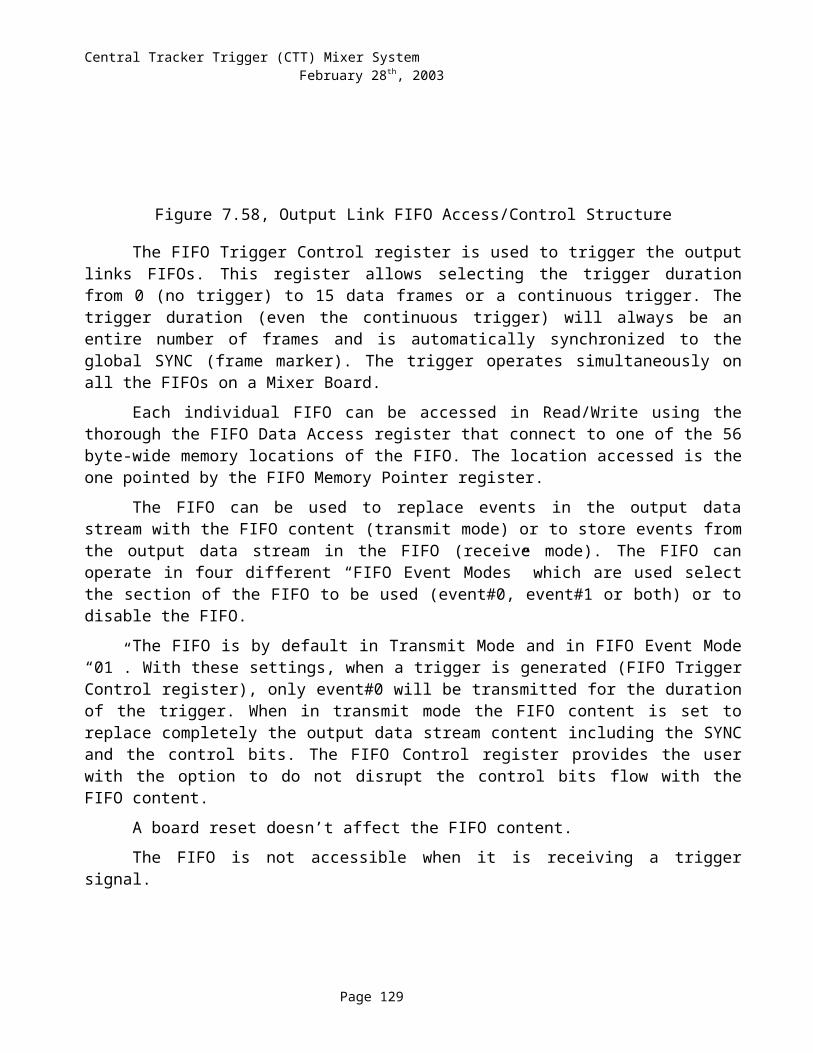
Central Tracker Trigger (CTT) Mixer System February 28th, 2003
Absolute Cassette#45
Relative Cassette#5
Absolute Cassette#46
Relative Cassette#4
L/R AFE Link# Mixer Slot #[MB#]
Mixer Link#
Super Sector
#L/R AFE
Link#Mixer Slot #
[MB#]Mixer Link#
Super Sector
#L 1 9 [4] 4 5 L 1 9 [4] 2 5L 2 9 [4] 14 5 L 2 8 [3] 2 5L 3 8 [3] 15 5 L 3 7 [2] 2 5L 4 6 [1] 11 5 L 4 6 [1] 2 5R 1 6 [1] 14 5 R 1 6 [1] 3 5R 2 8 [3] 14 5 R 2 7 [2] 3 5R 3 9 [4] 5 5 R 3 8 [3] 3 5R 4 9 [4] 6 5 R 4 9 [4] 3 5
Table 13.73, AFE Cassettes 45 and 46
Absolute Cassette#47
Relative Cassette#8
Absolute Cassette#48
Relative Cassette#7
L/R AFE Link# Mixer Slot #[MB#]
Mixer Link#
Super Sector
#L/R AFE
Link#Mixer Slot #
[MB#]Mixer Link#
Super Sector
#L 1 6 [1] 9 5 L 1 9 [4] 7 5L 2 7 [2] 15 5 L 2 9 [4] 9 5L 3 7 [2] 6 5 L 3 8 [3] 12 5L 4 8 [3] 4 5 L 4 6 [1] 7 5R 1 8 [3] 5 5 R 1 7 [2] 14 5R 2 7 [2] 13 5 R 2 8 [3] 7 5R 3 7 [2] 7 5 R 3 9 [4] 11 5R 4 6 [1] 4 5 R 4 9 [4] 1 5
Table 13.74, AFE Cassettes 47 and 48
Absolute Cassette#49
Relative Cassette#3
Absolute Cassette#50
Relative Cassette#2
L/R AFE Link# Mixer Slot #[MB#]
Mixer Link#
Super Sector
#L/R AFE
Link#Mixer Slot #
[MB#]Mixer Link#
Super Sector
#L 1 6 [1] 10 5 L 1 8 [3] 13 5L 2 7 [2] 5 5 L 2 8 [3] 9 5L 3 8 [3] 8 5 L 3 7 [2] 8 5L 4 9 [4] 12 5 L 4 6 [1] 1 5R 1 9 [4] 10 5 R 1 6 [1] 5 5R 2 8 [3] 11 5 R 2 7 [2] 4 5R 3 7 [2] 12 5 R 3 8 [3] 1 5R 4 6 [1] 8 5 R 4 9 [4] 8 5
Table 13.75, AFE Cassettes 49 and 50
Page 129

Central Tracker Trigger (CTT) Mixer System February 28th, 2003
Absolute Cassette#51
Relative Cassette#1
Absolute Cassette#52
Relative Cassette#3
L/R AFE Link# Mixer Slot #[MB#]
Mixer Link#
Super Sector
#L/R AFE
Link#Mixer Slot #
[MB#]Mixer Link#
Super Sector
#L 1 9 [4] 15 5 L 1 2 [1] 10 4L 2 6 [1] 15 5 L 2 3 [2] 5 4L 3 L 3 4 [3] 8 4L 4 L 4 5 [4] 12 4R 1 R 1 5 [4] 10 4R 2 R 2 4 [3] 11 4R 3 6 [1] 13 5 R 3 3 [2] 12 4R 4 9 [4] 13 5 R 4 2 [1] 8 4
Table 13.76, AFE Cassettes 51 and 52
Absolute Cassette#53
Relative Cassette#7
Absolute Cassette#54
Relative Cassette#2
L/R AFE Link# Mixer Slot #[MB#]
Mixer Link#
Super Sector
#L/R AFE
Link#Mixer Slot #
[MB#]Mixer Link#
Super Sector
#L 1 5 [4] 7 4 L 1 4 [3] 13 4L 2 5 [4] 9 4 L 2 4 [3] 9 4L 3 4 [3] 12 4 L 3 3 [2] 8 4L 4 2 [1] 7 4 L 4 2 [1] 1 4R 1 3 [2] 14 4 R 1 2 [1] 5 4R 2 4 [3] 7 4 R 2 3 [2] 4 4R 3 5 [4] 11 4 R 3 4 [3] 1 4R 4 5 [4] 1 4 R 4 5 [4] 8 4
Table 13.77, AFE Cassettes 53 and 54
Absolute Cassette#55
Relative Cassette#4
Absolute Cassette#56
Relative Cassette#5
L/R AFE Link# Mixer Slot #[MB#]
Mixer Link#
Super Sector
#L/R AFE
Link#Mixer Slot #
[MB#]Mixer Link#
Super Sector
#L 1 5 [4] 2 4 L 1 5 [4] 4 4L 2 4 [3] 2 4 L 2 5 [4] 14 4L 3 3 [2] 2 4 L 3 4 [3] 15 4L 4 2 [1] 2 4 L 4 2 [1] 11 4R 1 2 [1] 3 4 R 1 2 [1] 14 4R 2 3 [2] 3 4 R 2 4 [3] 14 4R 3 4 [3] 3 4 R 3 5 [4] 5 4R 4 5 [4] 3 4 R 4 5 [4] 6 4
Table 13.78, AFE Cassettes 55 and 56
Page 130

Central Tracker Trigger (CTT) Mixer System February 28th, 2003
Absolute Cassette#57
Relative Cassette#6
Absolute Cassette#58
Relative Cassette#8
L/R AFE Link# Mixer Slot #[MB#]
Mixer Link#
Super Sector
#L/R AFE
Link#Mixer Slot #
[MB#]Mixer Link#
Super Sector
#L 1 2 [1] 12 4 L 1 2 [1] 9 4L 2 3 [2] 9 4 L 2 3 [2] 15 4L 3 3 [2] 10 4 L 3 3 [2] 6 4L 4 4 [3] 6 4 L 4 4 [3] 4 4R 1 4 [3] 10 4 R 1 4 [3] 5 4R 2 3 [2] 11 4 R 2 3 [2] 13 4R 3 3 [2] 1 4 R 3 3 [2] 7 4R 4 2 [1] 6 4 R 4 2 [1] 4 4
Table 13.79, AFE Cassettes 57 and 58
Absolute Cassette#59
Relative Cassette#1
Absolute Cassette#60
Relative Cassette#2
L/R AFE Link# Mixer Slot #[MB#]
Mixer Link#
Super Sector
#L/R AFE
Link#Mixer Slot #
[MB#]Mixer Link#
Super Sector
#L 1 5 [4] 15 4 L 1 20 [3] 13 3L 2 2 [1] 15 4 L 2 20 [3] 9 3L 3 21 [4] 15 3 L 3 19 [2] 8 3L 4 18 [1] 15 3 L 4 18 [1] 1 3R 1 18 [1] 13 3 R 1 18 [1] 5 3R 2 21 [4] 13 3 R 2 19 [2] 4 3R 3 2 [1] 13 4 R 3 20 [3] 1 3R 4 5 [4] 13 4 R 4 21 [4] 8 3
Table 13.80, AFE Cassettes 59 and 60
Absolute Cassette#61
Relative Cassette#3
Absolute Cassette#62
Relative Cassette#4
L/R AFE Link# Mixer Slot #[MB#]
Mixer Link#
Super Sector
#L/R AFE
Link#Mixer Slot #
[MB#]Mixer Link#
Super Sector
#L 1 18 [1] 10 3 L 1 21 [4] 2 3L 2 19 [2] 5 3 L 2 20 [3] 2 3L 3 20 [3] 8 3 L 3 19 [2] 2 3L 4 21 [4] 12 3 L 4 18 [1] 2 3R 1 21 [4] 10 3 R 1 18 [1] 3 3R 2 20 [3] 11 3 R 2 19 [2] 3 3R 3 19 [2] 12 3 R 3 20 [3] 3 3R 4 18 [1] 8 3 R 4 21 [4] 3 3
Table 13.81, AFE Cassettes 61 and 62
Page 131

Central Tracker Trigger (CTT) Mixer System February 28th, 2003
Absolute Cassette#63
Relative Cassette#5
Absolute Cassette#64
Relative Cassette#6
L/R AFE Link# Mixer Slot #[MB#]
Mixer Link#
Super Sector
#L/R AFE
Link#Mixer Slot #
[MB#]Mixer Link#
Super Sector
#L 1 21 [4] 4 3 L 1 18 [1] 12 3L 2 21 [4] 14 3 L 2 19 [2] 9 3L 3 20 [3] 15 3 L 3 19 [2] 10 3L 4 18 [1] 11 3 L 4 20 [3] 6 3R 1 18 [1] 14 3 R 1 20 [3] 10 3R 2 20 [3] 14 3 R 2 19 [2] 11 3R 3 21 [4] 5 3 R 3 19 [2] 1 3R 4 21 [4] 6 3 R 4 18 [1] 6 3
Table 13.82, AFE Cassettes 63 and 64
Absolute Cassette#65
Relative Cassette#7
Absolute Cassette#66
Relative Cassette#8
L/R AFE Link# Mixer Slot #[MB#]
Mixer Link#
Super Sector
#L/R AFE
Link#Mixer Slot #
[MB#]Mixer Link#
Super Sector
#L 1 21 [4] 7 3 L 1 18 [1] 9 3L 2 21 [4] 9 3 L 2 19 [2] 15 3L 3 20 [3] 12 3 L 3 19 [2] 6 3L 4 18 [1] 7 3 L 4 20 [3] 4 3R 1 19 [2] 14 3 R 1 20 [3] 5 3R 2 20 [3] 7 3 R 2 19 [2] 13 3R 3 21 [4] 11 3 R 3 19 [2] 7 3R 4 21 [4] 1 3 R 4 18 [1] 4 3
Table 13.83, AFE Cassettes 65 and 66
Absolute Cassette# 68
Relative Cassette# CPS
Absolute Cassette# 70
Relative Cassette# CPS
L/R AFE Link# Mixer Slot #[MB#]
Mixer Link#
Super Sector
#L/R AFE
Link#Mixer Slot #
[MB#]Mixer Link#
Super Sector
#L 1 L 1L 2 21 [4] 0 3 L 2 5 [4] 0 4L 3 19 [2] 0 3 L 3 3 [2] 0 4L 4 L 4R 1 R 1R 2 18 [1] 0 3 R 2 2 [1] 0 4R 3 20 [3] 0 3 R 3 4 [3] 0 4R 4 R 4
Table 13.84, AFE Cassettes 68 (CPS) and 70 (CPS).
Page 132

Central Tracker Trigger (CTT) Mixer System February 28th, 2003
Absolute Cassette# 72
Relative Cassette# CPS
L/R AFE Link# Mixer Slot #[MB#]
Mixer Link#
Super Sector
#L 1L 2 9 [4] 0 5L 3 7 [2] 0 5L 4R 1R 2 6 [1] 0 5R 3 8 [3] 0 5R 4
Table 13.85, AFE Cassette 72 (CPS).
Relative Absolute Cassette NumberCassette# Super sector 1 Super sector 2 Super sector 3 Super sector 4 Super sector 5
1 36(Module 1-4) 36(Module 5-8) 59(Module 1-4) 59(Module 5-8) 51(Module 5-8)2 37 35 60 54 503 38 34 61 52 494 40 31 62 55 465 41 30 63 56 456 42 29 64 57 447 39 33 65 53 488 43 32 66 58 47
CPS 26 28 68 70 72
Table 13.86, Relative and Absolute Cassette numbers.
Page 133

Central Tracker Trigger (CTT) Mixer System February 28th, 2003
13.3 Mixer System Output Links cabling map
Mixer board output links arrangement on the front panel
DFE board input links arrangement on the front panel
Mixer Link#
Link Color[DFE Link#]
Mixer Link PORT#
(for cabling)DFE Link# Link Color
DFE Link PORT# (for cabling)
Row of pins used for JTAG 1 unused row of pins17 Red [0] 1 0 Red (copy) 116 Red [5] 2 2 unused row of pins15 Blue [7] 3 1 not used. 214 Yellow [6] 4 2 unused row of pins13 Purple [3] 5 2 Orange 312 Orange [2] 6 2 unused row of pins11 Green [4] 7 4 Green 410 Green [9] 8 2 unused row of pins
Unused row of pins 3 Purple 507 Red [0] 9 2 unused row of pins06 Red [5] 10 5 Red 605 Blue [7] 11 2 unused row of pins04 Yellow [6] 12 7 Blue 703 Purple [3] 13 2 unused row of pins02 Orange [2] 14 6 Yellow 801 Green [4] 15 2 unused row of pins00 Green [9] 16 8 not used 9
2 unused row of pins
9 Green (copy) 10
1 unused row of pins
Table 13.87, Mixer Board output links and DFE input links arrangements on the front panels.
Page 134
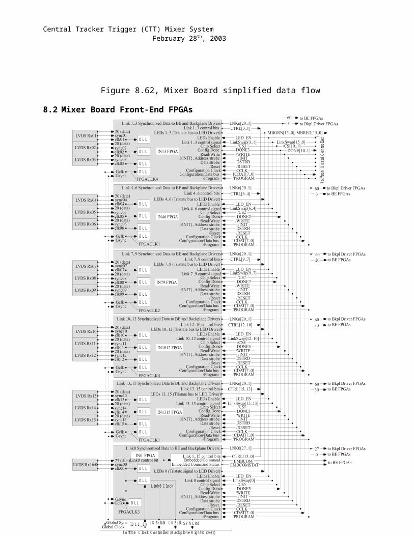
Central Tracker Trigger (CTT) Mixer System February 28th, 2003
Slot# 2 MB# 1 Supersector# 4 Slot# 3 MB# 2 Supersector# 4Mixer Link#
Color[DFE Link#, Port#]
DFE Subrack DFE Slot
Mixer Link#
Color[DFE Link#, Port#]
DFE Subrack DFE Slot
17 Red [L0-P1] PC03-3 4 17 Red [L0-P1] PC03-3 616 Red [L5-P6] PC03-3 3 16 Red [L5-P6] PC03-3 515 Blue [L7-P7] PC03-3 3 15 Blue [L7-P7] PC03-3 514 Yellow [L6-P8] PC03-3 3 14 Yellow [L6-P8] PC03-3 513 Purple [L3-P5] PC03-3 3 13 Purple [L3-P5] PC03-3 512 Orange [L2-P3] PC03-3 3 12 Orange [L2-P3] PC03-3 511 Green [L4-P4] PC03-3 3 11 Green [L4-P4] PC03-3 510 Green [L9-P10] PC03-3 2 10 Green [L9-P10] PC03-3 4
07 Red [L0-P1] PC03-3 3 07 Red [L0-P1] PC03-3 506 Red [L5-P6] PC03-3 2 06 Red [L5-P6] PC03-3 405 Blue [L7-P7] PC03-3 2 05 Blue [L7-P7] PC03-3 404 Yellow [L6-P8] PC03-3 2 04 Yellow [L6-P8] PC03-3 403 Purple [L3-P5] PC03-3 2 03 Purple [L3-P5] PC03-3 402 Orange [L2-P3] PC03-3 2 02 Orange [L2-P3] PC03-3 401 Green [L4-P4] PC03-3 2 01 Green [L4-P4] PC03-3 400 Green [L9-P10] PC03-2 21 00 Green [L9-P10] PC03-3 3
Table 13.88, Slot#2 and Slot#3 (Supersector#4).
Slot# 4 MB# 3 Supersector# 4 Slot# 5 MB# 4 Supersector# 4Mixer Link#
Color[DFE Link#, Port#]
DFE Subrack DFE Slot
Mixer Link#
Color[DFE Link#, Port#]
DFE Subrack DFE Slot
17 Red [L0-P1] PC03-3 8 17 Red [L0-P1] PC03-3 1016 Red [L5-P6] PC03-3 7 16 Red [L5-P6] PC03-3 915 Blue [L7-P7] PC03-3 7 15 Blue [L7-P7] PC03-3 914 Yellow [L6-P8] PC03-3 7 14 Yellow [L6-P8] PC03-3 913 Purple [L3-P5] PC03-3 7 13 Purple [L3-P5] PC03-3 912 Orange [L2-P3] PC03-3 7 12 Orange [L2-P3] PC03-3 911 Green [L4-P4] PC03-3 7 11 Green [L4-P4] PC03-3 910 Green [L9-P10] PC03-3 6 10 Green [L9-P10] PC03-3 8
07 Red [L0-P1] PC03-3 7 07 Red [L0-P1] PC03-3 906 Red [L5-P6] PC03-3 6 06 Red [L5-P6] PC03-3 805 Blue [L7-P7] PC03-3 6 05 Blue [L7-P7] PC03-3 804 Yellow [L6-P8] PC03-3 6 04 Yellow [L6-P8] PC03-3 803 Purple [L3-P5] PC03-3 6 03 Purple [L3-P5] PC03-3 802 Orange [L2-P3] PC03-3 6 02 Orange [L2-P3] PC03-3 801 Green [L4-P4] PC03-3 6 01 Green [L4-P4] PC03-3 800 Green [L9-P10] PC03-3 5 00 Green [L9-P10] PC03-3 7
Table 13.89, Slot#4 and Slot#5 (Supersector#4).
Page 135

Central Tracker Trigger (CTT) Mixer System February 28th, 2003
Slot# 6 MB# 1 Supersector# 5 Slot# 7 MB# 2 Supersector# 5Mixer Link#
Color[DFE Link#, Port#]
DFE Subrack DFE Slot
Mixer Link#
Color[DFE Link#, Port#]
DFE Subrack DFE Slot
17 Red [L0-P1] PC03-3 12 17 Red [L0-P1] PC03-3 1416 Red [L5-P6] PC03-3 11 16 Red [L5-P6] PC03-3 1315 Blue [L7-P7] PC03-3 11 15 Blue [L7-P7] PC03-3 1314 Yellow [L6-P8] PC03-3 11 14 Yellow [L6-P8] PC03-3 1313 Purple [L3-P5] PC03-3 11 13 Purple [L3-P5] PC03-3 1312 Orange [L2-P3] PC03-3 11 12 Orange [L2-P3] PC03-3 1311 Green [L4-P4] PC03-3 11 11 Green [L4-P4] PC03-3 1310 Green [L9-P10] PC03-3 10 10 Green [L9-P10] PC03-3 12
07 Red [L0-P1] PC03-3 11 07 Red [L0-P1] PC03-3 1306 Red [L5-P6] PC03-3 10 06 Red [L5-P6] PC03-3 1205 Blue [L7-P7] PC03-3 10 05 Blue [L7-P7] PC03-3 1204 Yellow [L6-P8] PC03-3 10 04 Yellow [L6-P8] PC03-3 1203 Purple [L3-P5] PC03-3 10 03 Purple [L3-P5] PC03-3 1202 Orange [L2-P3] PC03-3 10 02 Orange [L2-P3] PC03-3 1201 Green [L4-P4] PC03-3 10 01 Green [L4-P4] PC03-3 1200 Green [L9-P10] PC03-3 9 00 Green [L9-P10] PC03-3 11
Table 13.90, Slot#6 and Slot#7 (Supersector#5).
Slot# 8 MB# 3 Supersector# 5 Slot# 9 MB# 4 Supersector# 5Mixer Link#
Color[DFE Link#, Port#]
DFE Subrack DFE Slot
Mixer Link#
Color[DFE Link#, Port#]
DFE Subrack DFE Slot
17 Red [L0-P1] PC03-3 16 17 Red [L0-P1] PC03-3 1816 Red [L5-P6] PC03-3 15 16 Red [L5-P6] PC03-3 1715 Blue [L7-P7] PC03-3 15 15 Blue [L7-P7] PC03-3 1714 Yellow [L6-P8] PC03-3 15 14 Yellow [L6-P8] PC03-3 1713 Purple [L3-P5] PC03-3 15 13 Purple [L3-P5] PC03-3 1712 Orange [L2-P3] PC03-3 15 12 Orange [L2-P3] PC03-3 1711 Green [L4-P4] PC03-3 15 11 Green [L4-P4] PC03-3 1710 Green [L9-P10] PC03-3 14 10 Green [L9-P10] PC03-3 16
07 Red [L0-P1] PC03-3 15 07 Red [L0-P1] PC03-3 1706 Red [L5-P6] PC03-3 14 06 Red [L5-P6] PC03-3 1605 Blue [L7-P7] PC03-3 14 05 Blue [L7-P7] PC03-3 1604 Yellow [L6-P8] PC03-3 14 04 Yellow [L6-P8] PC03-3 1603 Purple [L3-P5] PC03-3 14 03 Purple [L3-P5] PC03-3 1602 Orange [L2-P3] PC03-3 14 02 Orange [L2-P3] PC03-3 1601 Green [L4-P4] PC03-3 14 01 Green [L4-P4] PC03-3 1600 Green [L9-P10] PC03-3 13 00 Green [L9-P10] PC03-3 15
Table 13.91, Slot#8 and Slot#9 (Supersector#5).
Page 136

Central Tracker Trigger (CTT) Mixer System February 28th, 2003
Slot# 10 MB# 1 Supersector# 1 Slot# 11 MB# 2 Supersector# 1Mixer Link#
Color[DFE Link#, Port#]
DFE Subrack DFE Slot
Mixer Link#
Color[DFE Link#, Port#]
DFE Subrack DFE Slot
17 Red [L0-P1] PC03-3 20 17 Red [L0-P1] PC03-2 216 Red [L5-P6] PC03-3 19 16 Red [L5-P6] PC03-3 2115 Blue [L7-P7] PC03-3 19 15 Blue [L7-P7] PC03-3 2114 Yellow [L6-P8] PC03-3 19 14 Yellow [L6-P8] PC03-3 2113 Purple [L3-P5] PC03-3 19 13 Purple [L3-P5] PC03-3 2112 Orange [L2-P3] PC03-3 19 12 Orange [L2-P3] PC03-3 2111 Green [L4-P4] PC03-3 19 11 Green [L4-P4] PC03-3 2110 Green [L9-P10] PC03-3 18 10 Green [L9-P10] PC03-3 20
07 Red [L0-P1] PC03-3 19 07 Red [L0-P1] PC03-3 2106 Red [L5-P6] PC03-3 18 06 Red [L5-P6] PC03-3 2005 Blue [L7-P7] PC03-3 18 05 Blue [L7-P7] PC03-3 2004 Yellow [L6-P8] PC03-3 18 04 Yellow [L6-P8] PC03-3 2003 Purple [L3-P5] PC03-3 18 03 Purple [L3-P5] PC03-3 2002 Orange [L2-P3] PC03-3 18 02 Orange [L2-P3] PC03-3 2001 Green [L4-P4] PC03-3 18 01 Green [L4-P4] PC03-3 2000 Green [L9-P10] PC03-3 17 00 Green [L9-P10] PC03-3 19
Table 13.92, Slot#10 and Slot#11 (Supersector#1).
Slot# 12 MB# 3 Supersector# 1 Slot# 13 MB# 4 Supersector# 1Mixer Link#
Color[DFE Link#, Port#]
DFE Subrack DFE Slot
Mixer Link#
Color[DFE Link#, Port#]
DFE Subrack DFE Slot
17 Red [L0-P1] PC03-2 4 17 Red [L0-P1] PC03-2 616 Red [L5-P6] PC03-2 3 16 Red [L5-P6] PC03-2 515 Blue [L7-P7] PC03-2 3 15 Blue [L7-P7] PC03-2 514 Yellow [L6-P8] PC03-2 3 14 Yellow [L6-P8] PC03-2 513 Purple [L3-P5] PC03-2 3 13 Purple [L3-P5] PC03-2 512 Orange [L2-P3] PC03-2 3 12 Orange [L2-P3] PC03-2 511 Green [L4-P4] PC03-2 3 11 Green [L4-P4] PC03-2 510 Green [L9-P10] PC03-2 2 10 Green [L9-P10] PC03-2 4
07 Red [L0-P1] PC03-2 3 07 Red [L0-P1] PC03-2 506 Red [L5-P6] PC03-2 2 06 Red [L5-P6] PC03-2 405 Blue [L7-P7] PC03-2 2 05 Blue [L7-P7] PC03-2 404 Yellow [L6-P8] PC03-2 2 04 Yellow [L6-P8] PC03-2 403 Purple [L3-P5] PC03-2 2 03 Purple [L3-P5] PC03-2 402 Orange [L2-P3] PC03-2 2 02 Orange [L2-P3] PC03-2 401 Green [L4-P4] PC03-2 2 01 Green [L4-P4] PC03-2 400 Green [L9-P10] PC03-3 21 00 Green [L9-P10] PC03-2 3
Table 13.93, Slot#12 and Slot#13 (Supersector#1).
Page 137

Central Tracker Trigger (CTT) Mixer System February 28th, 2003
Slot# 14 MB# 1 Supersector# 2 Slot# 15 MB# 2 Supersector# 2Mixer Link#
Color[DFE Link#, Port#]
DFE Subrack DFE Slot
Mixer Link#
Color[DFE Link#, Port#]
DFE Subrack DFE Slot
17 Red [L0-P1] PC03-2 8 17 Red [L0-P1] PC03-2 1016 Red [L5-P6] PC03-2 7 16 Red [L5-P6] PC03-2 915 Blue [L7-P7] PC03-2 7 15 Blue [L7-P7] PC03-2 914 Yellow [L6-P8] PC03-2 7 14 Yellow [L6-P8] PC03-2 913 Purple [L3-P5] PC03-2 7 13 Purple [L3-P5] PC03-2 912 Orange [L2-P3] PC03-2 7 12 Orange [L2-P3] PC03-2 911 Green [L4-P4] PC03-2 7 11 Green [L4-P4] PC03-2 910 Green [L9-P10] PC03-2 6 10 Green [L9-P10] PC03-2 8
07 Red [L0-P1] PC03-2 7 07 Red [L0-P1] PC03-2 906 Red [L5-P6] PC03-2 6 06 Red [L5-P6] PC03-2 805 Blue [L7-P7] PC03-2 6 05 Blue [L7-P7] PC03-2 804 Yellow [L6-P8] PC03-2 6 04 Yellow [L6-P8] PC03-2 803 Purple [L3-P5] PC03-2 6 03 Purple [L3-P5] PC03-2 802 Orange [L2-P3] PC03-2 6 02 Orange [L2-P3] PC03-2 801 Green [L4-P4] PC03-2 6 01 Green [L4-P4] PC03-2 800 Green [L9-P10] PC03-2 5 00 Green [L9-P10] PC03-2 7
Table 13.94, Slot#14 and Slot#15 (Supersector#2).
Slot# 16 MB# 3 Supersector# 2 Slot# 17 MB# 4 Supersector# 2Mixer Link#
Color[DFE Link#, Port#]
DFE Subrack DFE Slot
Mixer Link#
Color[DFE Link#, Port#]
DFE Subrack DFE Slot
17 Red [L0-P1] PC03-2 12 17 Red [L0-P1] PC03-2 1416 Red [L5-P6] PC03-2 11 16 Red [L5-P6] PC03-2 1315 Blue [L7-P7] PC03-2 11 15 Blue [L7-P7] PC03-2 1314 Yellow [L6-P8] PC03-2 11 14 Yellow [L6-P8] PC03-2 1313 Purple [L3-P5] PC03-2 11 13 Purple [L3-P5] PC03-2 1312 Orange [L2-P3] PC03-2 11 12 Orange [L2-P3] PC03-2 1311 Green [L4-P4] PC03-2 11 11 Green [L4-P4] PC03-2 1310 Green [L9-P10] PC03-2 10 10 Green [L9-P10] PC03-2 12
07 Red [L0-P1] PC03-2 11 07 Red [L0-P1] PC03-2 1306 Red [L5-P6] PC03-2 10 06 Red [L5-P6] PC03-2 1205 Blue [L7-P7] PC03-2 10 05 Blue [L7-P7] PC03-2 1204 Yellow [L6-P8] PC03-2 10 04 Yellow [L6-P8] PC03-2 1203 Purple [L3-P5] PC03-2 10 03 Purple [L3-P5] PC03-2 1202 Orange [L2-P3] PC03-2 10 02 Orange [L2-P3] PC03-2 1201 Green [L4-P4] PC03-2 10 01 Green [L4-P4] PC03-2 1200 Green [L9-P10] PC03-2 9 00 Green [L9-P10] PC03-2 11
Table 13.95, Slot#16 and Slot#17 (Supersector#2).
Page 138

Central Tracker Trigger (CTT) Mixer System February 28th, 2003
Slot# 18 MB# 1 Supersector# 3 Slot# 19 MB# 2 Supersector# 3Mixer Link#
Color[DFE Link#, Port#]
DFE Subrack DFE Slot
Mixer Link#
Color[DFE Link#, Port#]
DFE Subrack DFE Slot
17 Red [L0-P1] PC03-2 16 17 Red [L0-P1] PC03-2 1816 Red [L5-P6] PC03-2 15 16 Red [L5-P6] PC03-2 1715 Blue [L7-P7] PC03-2 15 15 Blue [L7-P7] PC03-2 1714 Yellow [L6-P8] PC03-2 15 14 Yellow [L6-P8] PC03-2 1713 Purple [L3-P5] PC03-2 15 13 Purple [L3-P5] PC03-2 1712 Orange [L2-P3] PC03-2 15 12 Orange [L2-P3] PC03-2 1711 Green [L4-P4] PC03-2 15 11 Green [L4-P4] PC03-2 1710 Green [L9-P10] PC03-2 14 10 Green [L9-P10] PC03-2 16
07 Red [L0-P1] PC03-2 15 07 Red [L0-P1] PC03-2 1706 Red [L5-P6] PC03-2 14 06 Red [L5-P6] PC03-2 1605 Blue [L7-P7] PC03-2 14 05 Blue [L7-P7] PC03-2 1604 Yellow [L6-P8] PC03-2 14 04 Yellow [L6-P8] PC03-2 1603 Purple [L3-P5] PC03-2 14 03 Purple [L3-P5] PC03-2 1602 Orange [L2-P3] PC03-2 14 02 Orange [L2-P3] PC03-2 1601 Green [L4-P4] PC03-2 14 01 Green [L4-P4] PC03-2 1600 Green [L9-P10] PC03-2 13 00 Green [L9-P10] PC03-2 15
Table 13.96, Slot#18 and Slot#19 (Supersector#3).
Slot# 20 MB# 3 Supersector# 3 Slot# 21 MB# 4 Supersector# 3Mixer Link#
Color[DFE Link#, Port#]
DFE Subrack DFE Slot
Mixer Link#
Color[DFE Link#, Port#]
DFE Subrack DFE Slot
17 Red [L0-P1] PC03-2 20 17 Red [L0-P1] PC03-3 216 Red [L5-P6] PC03-2 19 16 Red [L5-P6] PC03-2 2115 Blue [L7-P7] PC03-2 19 15 Blue [L7-P7] PC03-2 2114 Yellow [L6-P8] PC03-2 19 14 Yellow [L6-P8] PC03-2 2113 Purple [L3-P5] PC03-2 19 13 Purple [L3-P5] PC03-2 2112 Orange [L2-P3] PC03-2 19 12 Orange [L2-P3] PC03-2 2111 Green [L4-P4] PC03-2 19 11 Green [L4-P4] PC03-2 2110 Green [L9-P10] PC03-2 18 10 Green [L9-P10] PC03-2 20
07 Red [L0-P1] PC03-2 19 07 Red [L0-P1] PC03-2 2106 Red [L5-P6] PC03-2 18 06 Red [L5-P6] PC03-2 2005 Blue [L7-P7] PC03-2 18 05 Blue [L7-P7] PC03-2 2004 Yellow [L6-P8] PC03-2 18 04 Yellow [L6-P8] PC03-2 2003 Purple [L3-P5] PC03-2 18 03 Purple [L3-P5] PC03-2 2002 Orange [L2-P3] PC03-2 18 02 Orange [L2-P3] PC03-2 2001 Green [L4-P4] PC03-2 18 01 Green [L4-P4] PC03-2 2000 Green [L9-P10] PC03-2 17 00 Green [L9-P10] PC03-2 19
Table 13.97, Slot#20 and Slot#21 (Supersector#3).
Page 139

Central Tracker Trigger (CTT) Mixer System February 28th, 2003
14. Appendix H – Subrack Controller
14.1 Subrack Controller
Most of the subrack controller information is derived from [Ref. 5].
The Digital Front End Controller (DFEC) sits in slot 1 of the DFE and Mixer subracks, and is responsible for downloading device configuration data files to DFE motherboards and Mixer boards. Additionally, the DFEC monitors the status of the boards in the subrack and makes this data available (via a 1553 interface) to the DZERO slow monitoring system.
The primary function of the DFEC is to quickly download configuration data to the devices on the DFE motherboards and Mixer boards.
Each subrack hosts 20 boards, and each board can have up to 16 devices. Furthermore, the firmware in each of the devices may be unique, thus the controller must be able to manage configuration files for up to 320 devices. For diagnostic reasons, the DFEC board includes enough non-volatile memory (CompactFlash™ card) so that at least two configuration files for each device can be stored locally. The Mixer subrack requires a 128MB or 64MB CompactFlash™ card.
The DFEC uses MSDOS FAT16 file system, allowing for easy file transfers directly to and from the CompactFlash™ card using a commercially available card reader. Files can also be accessed over the 1553 network once the DFEC is installed on the D0 detector platform.
Communications between the Mixer and DFE subracks and the outside world occur through a 1553 interface. The DFEC appears on the 1553 network as a single Remote Terminal (RT). The 1553 bus master can read and write to a small dual port memory located on the DFEC. Using a dual port memory allows for greater decoupling between the 1553 protocol timing and the DFEC microcontroller.
Essentially the DFEC microcontroller acts as a command processor. The 1553 master writes commands and data into the dual port memory, and then generates an interrupt on the microcontroller. The microcontroller wakes up, executes the command(s) and then goes back to idle [Ref. 5d].
Basic status information is read from the Mixer and DFE boards over a dedicated slow monitoring serial bus. This information is continually being collected on the DFEC and made available to the 1553 host. The information collected from the mixer system boards is described in paragraph 4.6.
The DFEC communicates with the Mixer boards over a simple 16-bit address 8-bit data bus (Paragraph 4.5). This bus is not VME compatible.
An Atmel ATMEGA103 is used on the DFEC. It is flash based and supports in-system programmability and contains a debugger that allows the user to step through the code one instruction at a time and set breakpoints, etc. The microcontroller on the DFEC runs off of a 6MHz clock.
Page 140

Central Tracker Trigger (CTT) Mixer System February 28th, 2003
Figure 14.93, Subrack controller simplified block diagram
Figure 14.94, Subrack Controller (DFEC) Status Word.
Page 141
R e m o teTe rm in a lA d d ress
1 5 5 3 In te rface
ad d re ss F u n c tio n0 0 0 0 h0 0 0 1 h
0 0 7 F h
D F E C s ta tu s w o rdco m m an d b u ffe r
S u bad d re ss
1 6 (1 0 h )1 7 (11 h )1 8 (1 2 h )
ad dre ss p o in te r (read /w rite )d a ta reg is te r (read /w rite )D F E C S ta tu s W o rd (rea d), ex ecu te co m m an d s (w rite )
0 0 8 0 h
0 0 FA h0 0 F 9 h
0 1 0 0 h0 0 F F h
0 1 F F h
b o ard s ta tu s b lo c k
sec to r b u ffe r
M em o ry m ap
T h e a d d ress p o in te ris inc rem en ted
each tim e th e d a tare g is te r is a c ce ssed
128MB
MEMORY CARDCompactFlash TM
B ac kp la n eS lo w M o n ito rin g
In te rface
B ackp la n eG e n era l P u rp o se B u s
In te rfa ce
g ene ra l p u rp o se m em o ry
M icro con tro lle r
| 1 5 1 4 1 3 1 2 | 11 1 0 9 8 | 7 6 5 4 | 3 2 1 0 |
D F E C S ta tu s W ord
F U L : C o m p ac t F la sh F U L L
H A LT: co m m a n d o r co m m an d a rg u m en t e rro r
B U S Y: p ro ce ssin g co m m an d sID L E : co m m an d s ex ecu ted w ith n o e rro rs

128MB
MEMORY CARDCompactFlash TM
Central Tracker Trigger (CTT) Mixer System February 28th, 2003
14.2 CompactFlash™ card
The subrack controller uses a CompactFlash™ [Ref. 37] memory card to store the files needed for configuration of the mixer board FPGAs. The FPGA's configuration files are listed in Table 5.32. The memory card also stores up to ten files containing the sequence of commands to be executed by the subrack controller at power-up. Each command file can contains a maximum of 127 bytes, which match the length of the subrack controller command buffer.
The command files are numbered sequentially in the same order they will be executed; their filenames must be "autoexec.000" to "autoexec.009". The subrack controller will stop after executing "autoexec.009" or when the next command file in the sequence is not found.
Figure 14.95, CompactFlash card.
14.2.1 General information about Compact Flash cards [Ref. 15]
CompactFlash™ is a small removable mass storage device. First introduced in 1994 by SanDisk Corporation [Ref. 37], CF™ cards weigh a half-ounce and are the size of a matchbook (43mm [1.7"] x 36mm [1.4"] x 3.3mm [0.13"]).
CompactFlash cards are designed with flash technology, a non-volatile storage solution that does not require a battery to retain data indefinitely. CompactFlash storage products are solid state, meaning they contain no moving parts.
Dual 3.3V & 5V Operation – CompactFlash cards support both 3.3V and 5V operation and can be interchanged between 3.3V and 5V systems.
Shock – CF cards have an operating shock rating of 2,000 Gs, which is equivalent to a 10-foot drop. With typical usage, a CF card can be used for more than 100 years with no loss or deterioration of data.
Data Reliability – CompactFlash data is protected by built-in dynamic defect management and error correction technologies.
The CompactFlash card can be read/written with the SanDisk ImageMate™ external flash card reader that connects to a computer through a USB port. Another option is the SanDisk PCMCIA card adapter.
14.2.2 Standard subrack controller commands (autoexec) files
The following two tables describe the content of the two standard "autoexec" or "command" binary files stored on the CompactFlash card to handle the mixer board FPGAs configuration at
Page 142

Central Tracker Trigger (CTT) Mixer System February 28th, 2003
power-up. The files have been written using a Hex editor [Ref. 43]. Beside the autoexec files the CompactFlash contains the mixer board FPGA's configuration files.
Refer to paragraph 14.3 for a list of the subrack controller commands. The complete description of subrack controller is in available [Ref. 5].
command (0x) Notes
1200 8102Write byte 0x00 to backplane, offset 0x81 (subrack broadcasting to relative address 0x01 Device Status/Control register), slot# 02. This command will write to all the Mixer Boards setting the device select pointer to device 0x00.
5300 4202 0200Copy file to backplane, offset 0x42 (mixer board # broadcasting to relative address 0x02 Device Configuration Data register), slot# 02. This command will download to Mixer Boards in slot# 02, 06, 10, 14, 18 the Mixer1/device 00 configuration file "0200_PC.bin".
5300 4203 0300Copy file to backplane, offset 0x42 (mixer board # broadcasting to relative address 0x02 Device Configuration Data register), slot# 03. This command will download to Mixer Boards in slot# 03, 07, 11, 15, 19 the Mixer2/device 00 configuration file "0300_PC.bin".
5300 4204 0400 Copy file to backplane, offset 0x42, slot# 04. This command will download to Mixer Boards in slot# 04, 08, 12, 16, 20 the Mixer3/device 00 configuration file "0400_PC.bin".
5300 4205 0500 Copy file to backplane, offset 0x42, slot# 05. This command will download to Mixer Boards in slot# 05, 09, 13, 17, 21 the Mixer4/device 00 configuration file "0400_PC.bin".
1201 8102Write byte 0x01 to backplane, offset 0x81 (subrack broadcasting to relative address 0x01 Device Status/Control register), slot# 02. This command will write to all the Mixer Boards setting the device select pointer to device 0x01.
5300 4202 0201 Copy file to backplane, Mixer1/device 01 configuration file "0201_PC.bin".
5300 4203 0301 Copy file to backplane, Mixer2/device 01 configuration file "0301_PC.bin".
5300 4204 0401 Copy file to backplane, Mixer3/device 01 configuration file "0401_PC.bin".
5300 4205 0501 Copy file to backplane, Mixer4/device 01 configuration file "0501_PC.bin".
1202 8102 Write byte 0x02 to backplane. Sets the device select pointer to device 0x02 in all mixer boards.
5300 4202 0202 Copy file to backplane, Mixer1/device 02 configuration file "0202_PC.bin".
5300 4203 0302 Copy file to backplane, Mixer2/device 02 configuration file "0302_PC.bin".
5300 4204 0402 Copy file to backplane, Mixer3/device 02 configuration file "0402_PC.bin".
5300 4205 0502 Copy file to backplane, Mixer4/device 02 configuration file "0502_PC.bin".
1203 8102 Write byte 0x03 to backplane. Sets the device select pointer to device 0x03 in all mixer boards.
5300 4202 0203 Copy file to backplane, Mixer1/device 03 configuration file "0203_PC.bin".
5300 4203 0303 Copy file to backplane, Mixer2/device 03 configuration file "0303_PC.bin".
5300 4204 0403 Copy file to backplane, Mixer3/device 03 configuration file "0403_PC.bin".
5300 4205 0503 Copy file to backplane, Mixer4/device 03 configuration file "0503_PC.bin".
1204 8102 Write byte 0x04 to backplane. Sets the device select pointer to device 0x04 in all mixer boards.
5300 4202 0204 Copy file to backplane, Mixer1/device 04 configuration file "0204_PC.bin".
5300 4203 0304 Copy file to backplane, Mixer2/device 04 configuration file "0304_PC.bin".
5300 4204 0404 Copy file to backplane, Mixer3/device 04 configuration file "0404_PC.bin".
5300 4205 0504 Copy file to backplane, Mixer4/device 04 configuration file "0504_PC.bin".
Page 143

Central Tracker Trigger (CTT) Mixer System February 28th, 2003
1205 8102 Write byte 0x05 to backplane. Sets the device select pointer to device 0x05 in all mixer boards.
5300 4202 0205 Copy file to backplane, Mixer1/device 05 configuration file "0205_PC.bin".
5300 4203 0305 Copy file to backplane, Mixer2/device 05 configuration file "0305_PC.bin".
5300 4204 0405 Copy file to backplane, Mixer3/device 05 configuration file "0405_PC.bin".
5300 4205 0505 Copy file to backplane, Mixer4/device 05 configuration file "0505_PC.bin".
1206 8102 Write byte 0x06 to backplane. Sets the device select pointer to device 0x06 in all mixer boards.
5300 4202 0206 Copy file to backplane, Mixer1/device 06 configuration file "0206_PC.bin".
5300 4203 0306 Copy file to backplane, Mixer2/device 06 configuration file "0306_PC.bin".
5300 4204 0406 Copy file to backplane, Mixer3/device 06 configuration file "0406_PC.bin".
5300 4205 0506 Copy file to backplane, Mixer4/device 06 configuration file "0506_PC.bin".
1207 8102 Write byte 0x07 to backplane. Sets the device select pointer to device 0x07 in all mixer boards.
5300 4202 0207 Copy file to backplane, Mixer1/device 07 configuration file "0207_PC.bin".
5300 4203 0307 Copy file to backplane, Mixer2/device 07 configuration file "0307_PC.bin".
5300 4204 0407 Copy file to backplane, Mixer3/device 07 configuration file "0407_PC.bin".
5300 4205 0507 Copy file to backplane, Mixer4/device 07 configuration file "0507_PC.bin".
A100 End of list command. Stop the subrack controller execution of the commands in the command buffer and make him look for next autoexec file.
Table 14.98, content of file "autoexec.000".
command (0x) Notes
1208 8102 Write byte 0x08 to backplane. Sets the device select pointer to device 0x08 in all mixer boards.
5300 4202 0208 Copy file to backplane, Mixer1/device 08 configuration file "0208_PC.bin".
5300 4203 0308 Copy file to backplane, Mixer2/device 08 configuration file "0308_PC.bin".
5300 4204 0408 Copy file to backplane, Mixer3/device 08 configuration file "0408_PC.bin".
5300 4205 0508 Copy file to backplane, Mixer4/device 08 configuration file "0508_PC.bin".
1209 8102 Write byte 0x09 to backplane. Sets the device select pointer to device 0x09 in all mixer boards.
5300 4202 0209 Copy file to backplane, Mixer1/device 09 configuration file "0209_PC.bin".
5300 4203 0309 Copy file to backplane, Mixer2/device 09 configuration file "0309_PC.bin".
5300 4204 0409 Copy file to backplane, Mixer3/device 09 configuration file "0409_PC.bin".
5300 4205 0509 Copy file to backplane, Mixer4/device 09 configuration file "0509_PC.bin".
120A 8102 Write byte 0x0A to backplane. Sets the device select pointer to device 0x0A in all mixer boards.
5300 4202 020A Copy file to backplane, Mixer1/device 0A configuration file "020A_PC.bin".
5300 4203 030A Copy file to backplane, Mixer2/device 0A configuration file "030A_PC.bin".
5300 4204 040A Copy file to backplane, Mixer3/device 0A configuration file "040A_PC.bin".
5300 4205 050A Copy file to backplane, Mixer4/device 0A configuration file "050A_PC.bin".
120B 8102 Write byte 0x0B to backplane. Sets the device select pointer to device 0x0B in all mixer boards.
5300 4202 020B Copy file to backplane, Mixer1/device 0B configuration file "020B_PC.bin".
Page 144

Central Tracker Trigger (CTT) Mixer System February 28th, 2003
5300 4203 030B Copy file to backplane, Mixer2/device 0B configuration file "030B_PC.bin".
5300 4204 040B Copy file to backplane, Mixer3/device 0B configuration file "040B_PC.bin".
5300 4205 050B Copy file to backplane, Mixer4/device 0B configuration file "050B_PC.bin".
120C 8102 Write byte 0x0C to backplane. Sets the device select pointer to device 0x0C in all mixer boards.
5300 4202 020C Copy file to backplane, Mixer1/device 0C configuration file "020C_PC.bin".
5300 4203 030C Copy file to backplane, Mixer2/device 0C configuration file "030C_PC.bin".
5300 4204 040C Copy file to backplane, Mixer3/device 0C configuration file "040C_PC.bin".
5300 4205 050C Copy file to backplane, Mixer4/device 0C configuration file "050C_PC.bin".
120D 8102 Write byte 0x0D to backplane. Sets the device select pointer to device 0x0D in all mixer boards.
5300 4202 020D Copy file to backplane, Mixer1/device 0D configuration file "020D_PC.bin".
5300 4203 030D Copy file to backplane, Mixer2/device 0D configuration file "030D_PC.bin".
5300 4204 040D Copy file to backplane, Mixer3/device 0D configuration file "040D_PC.bin".
5300 4205 050D Copy file to backplane, Mixer4/device 0D configuration file "050D_PC.bin".
120E 8102 Write byte 0x0E to backplane. Sets the device select pointer to device 0x0E in all mixer boards.
5300 4202 020E Copy file to backplane, Mixer1/device 0E configuration file "020E_PC.bin".
5300 4203 030E Copy file to backplane, Mixer2/device 0E configuration file "030E_PC.bin".
5300 4204 040E Copy file to backplane, Mixer3/device 0E configuration file "040E_PC.bin".
5300 4205 050E Copy file to backplane, Mixer4/device 0E configuration file "050E_PC.bin".
120F 8102 Write byte 0x0F to backplane. Sets the device select pointer to device 0x0F in all mixer boards.
5300 4202 020F Copy file to backplane, Mixer1/device 0F configuration file "020F_PC.bin".
5300 4203 030F Copy file to backplane, Mixer2/device 0F configuration file "030F_PC.bin".
5300 4204 040F Copy file to backplane, Mixer3/device 0F configuration file "040F_PC.bin".
5300 4205 050F Copy file to backplane, Mixer4/device 0F configuration file "050F_PC.bin".
A100 End of list command. Stop the subrack controller execution of the commands in the command buffer and make him look for next autoexec file.
Table 14.99, content of file "autoexec.001".
Page 145

Central Tracker Trigger (CTT) Mixer System February 28th, 2003
14.3 Subrack Controller Commands
The following tables provide the list of the subrack controller commands. For complete documentation refer to [Ref. 5].
Write Byte to Backplane Read Byte from Backplane
F E D C B A 9 8 7 6 5 4 3 2 1 0 bit# F E D C B A 9 8 7 6 5 4 3 2 1 0
0x1 0x2 data byte 1stword 0x2 0x2
offset slot number 2ndword offset slot number
CompactFlash to Sector Buffer SectorBuffer toCompactFlash
F E D C B A 9 8 7 6 5 4 3 2 1 0 bit # F E D C B A 9 8 7 6 5 4 3 2 1 0
0x3 0x2 lba high byte 1stword 0x4 0x2 lba high byte
lba mid byte lba low byte 2ndword lba mid byte lba low byte
Copy File to Backplane Delete File from CompactFlash
F E D C B A 9 8 7 6 5 4 3 2 1 0 bit # F E D C B A 9 8 7 6 5 4 3 2 1 0
0x5 0x3 1stword 0x9 0x2
offset slot number 2ndword file name
file name 3rd word
Append Sector to File Generate File Checksum
F E D C B A 9 8 7 6 5 4 3 2 1 0 bit # F E D C B A 9 8 7 6 5 4 3 2 1 0
0x8 0x2 1stword 0x7 0x2
file name 2ndword file name
Reset Board Set Clock Bits
F E D C B A 9 8 7 6 5 4 3 2 1 0 bit # F E D C B A 9 8 7 6 5 4 3 2 1 0
0x7 0x1 slot number 1stword 0xC 0x1 clk slot number
Configure Device Get Firmware Revision
F E D C B A 9 8 7 6 5 4 3 2 1 0 bit # F E D C B A 9 8 7 6 5 4 3 2 1 0
0x6 0x3 slot number 1stword 0xB 0x2 slot number
device # firmware rev byte 2ndword device #
file name 3rdword
Page 146

Central Tracker Trigger (CTT) Mixer System February 28th, 2003
NOP Command Get File Size
F E D C B A 9 8 7 6 5 4 3 2 1 0 bit # F E D C B A 9 8 7 6 5 4 3 2 1 0
0xF 0x1 1stword 0xD 0x2
2ndword file name
End of List
F E D C B A 9 8 7 6 5 4 3 2 1 0 bit #
0xA 0x1 0x0 1stword
14.3.1 Examples of command usage
command (0x) Notes
1202 0015 Write 0x02 to the Board Status/Control register of mixer board in slot# 21 (0x15). This operation will force the board in the reset state. The FPGAs configuration will be retained.
1200 0015 Write 0x00 to the Board Status/Control register of mixer board in slot# 21 (0x15). The mixer board will be forced out of the reset state and resume normal operations.
Table 14.100, Example of mixer board reset operation.
command (0x) Notes
1200 8B0C Write 0x00 to the Monitoring Mode register of all mixer boards. This operation will change the LED monitoring mode to mode#0 (input links clock and DLL status).
Table 14.101, Example of change LED monitoring mode operation.
command (0x) Notes
1217 2409Write 0x17 to the Mode of Operation register (address 0x04) of the boards in the second mixer subsystem (slot# 6, 7, 8, 9). This operation enables the "Device Access Registers", allowing to access registers located on mixer board FPGAs.
120A 2109Write 0x0A to the Device Status/Control register (address 0x01) of the boards in the second mixer subsystem (slot# 6, 7, 8, 9). This operation point the board controller to talk to device# 0A (IN0 FPGA)
12<reg> 2709
Write <reg> to the Device Access Address register (address 0x07) of the boards in the second mixer subsystem (slot# 6, 7, 8, 9). This operation point the board controller to talk to the specific register address <reg> inside the device specified in the previous operation.
If the LED monitoring mode is set to mode 8 the front panel LEDs 0..7 will display the content of the local bus that is continuously driven by the content of the register <reg> of device #0A.
2200 0806 Readback the content of the Device Access Data register on the mixer board in slot #6. The byte read is the content of register <reg> inside device# 0A.
12<data_byte> 0806 Write <data_byte> to the Device Access Data register on the mixer board in slot #6. This operation will write the <data_byte> to the register <reg> of device #0A.
Table 14.102, Example of device access operations.
Page 147

Central Tracker Trigger (CTT) Mixer System February 28th, 2003
14.4 Test procedures information
A separate document provides [Ref. 8c] information on mixer board/system test procedures.
14.5 Diagnostic procedures information
A separate document provides [Ref. 8d] information and examples on mixer system diagnostic procedures.
Page 148

Central Tracker Trigger (CTT) Mixer System February 28th, 2003
15. Appendix I – CPS re-mapping conversion tables
The following 4 four tables provide the re-mapping information for the CPS data bits received by the mixer system. The original CPS data stream was sent to each mixer board over a 28 bit wide links (one of the 28 bits is used for frame synchronization). The new CPS data stream will be sent over a 21 bit wide data stream (one of the 21 bits used for frame synchronization). The original data stream had a total of 128 data bits per frame (seven clock cycles), the new one has only 64 data bits per frame.
Data bits marked as "X" (blue background color) are lost due to 28 to 21 bits re-mapping.
Data bits marked as "S" (gray background color) are still handled by the mixer but will not be used by the AFEs to send data and will be ignored by the DFEs.
Re-mapping of the CPS link data bits sent to Mixer 1
old designation
new designation
old designation
new designation
old designation
new designation
old designation
new designation
CPSL1 CPS1 CPSL33 CPS33 CPSH1 CPS6 CPSH33 SCPSL2 CPS2 CPSL34 CPS34 CPSH2 CPS7 CPSH34 CPS41CPSL3 CPS3 CPSL35 CPS35 CPSH3 CPS8 CPSH35 SCPSL4 CPS4 CPSL36 CPS36 CPSH4 CPS9 CPSH36 CPS43CPSL5 S CPSL37 CPS37 CPSH5 CPS10 CPSH37 SCPSL6 CPS5 CPSL38 CPS38 CPSH6 S CPSH38 CPS40CPSL7 S CPSL39 CPS39 CPSH7 S CPSH39 CPS42CPSL8 S CPSL40 S CPSH8 X CPSH40 XCPSL9 CPS11 CPSL41 X CPSH9 X CPSH41 CPS44
CPSL10 CPS12 CPSL42 X CPSH10 X CPSH42 CPS45CPSL11 CPS13 CPSL43 X CPSH11 X CPSH43 CPS46CPSL12 CPS14 CPSL44 X CPSH12 X CPSH44 CPS47CPSL13 CPS15 CPSL45 X CPSH13 X CPSH45 CPS48CPSL14 CPS16 CPSL46 X CPSH14 X CPSH46 CPS49CPSL15 S CPSL47 X CPSH15 X CPSH47 CPS50CPSL16 S CPSL48 X CPSH16 S CPSH48 SCPSL17 CPS17 CPSL49 X CPSH17 S CPSH49 CPS51CPSL18 S CPSL50 X CPSH18 CPS21 CPSH50 CPS52CPSL19 CPS18 CPSL51 X CPSH19 S CPSH51 CPS53CPSL20 CPS19 CPSL52 X CPSH20 S CPSH52 SCPSL21 S CPSL53 X CPSH21 CPS22 CPSH53 SCPSL22 CPS20 CPSL54 X CPSH22 S CPSH54 CPS54CPSL23 X CPSL55 S CPSH23 S CPSH55 SCPSL24 X CPSL56 S CPSH24 S CPSH56 SCPSL25 CPS23 CPSL57 CPS55 CPSH25 S CPSH57 CPS62CPSL26 CPS24 CPSL58 CPS56 CPSH26 S CPSH58 CPS63CPSL27 CPS25 CPSL59 CPS57 CPSH27 S CPSH59 SCPSL28 CPS26 CPSL60 CPS58 CPSH28 S CPSH60 CPS64CPSL29 CPS27 CPSL61 CPS59 CPSH29 CPS30 CPSH61 SCPSL30 CPS28 CPSL62 CPS60 CPSH30 CPS31 CPSH62 XCPSL31 CPS29 CPSL63 CPS61 CPSH31 CPS32 CPSH63 XCPSL32 S CPSL64 S CPSH32 S CPSH64 X
Table 15.103, Mixer 1 CPS data bits re-mapping.
Page 149

Central Tracker Trigger (CTT) Mixer System February 28th, 2003
Re-mapping of the CPS link data bits sent to Mixer 2
old designation
new designation
old designation
new designation
old designation
new designation
old designation
new designation
CPSL65 CPS65 CPSL97 CPS97 CPSH65 CPS70 CPSH97 SCPSL66 CPS66 CPSL98 CPS98 CPSH66 CPS71 CPSH98 CPS105CPSL67 CPS67 CPSL99 CPS99 CPSH67 CPS72 CPSH99 SCPSL68 CPS68 CPSL100 CPS100 CPSH68 CPS73 CPSH100 CPS107CPSL69 S CPSL101 CPS101 CPSH69 CPS74 CPSH101 SCPSL70 CPS69 CPSL102 CPS102 CPSH70 S CPSH102 CPS104CPSL71 S CPSL103 CPS103 CPSH71 S CPSH103 CPS106CPSL72 S CPSL104 S CPSH72 X CPSH104 XCPSL73 CPS75 CPSL105 X CPSH73 X CPSH105 CPS108CPSL74 CPS76 CPSL106 X CPSH74 X CPSH106 CPS109CPSL75 CPS77 CPSL107 X CPSH75 X CPSH107 CPS110CPSL76 CPS78 CPSL108 X CPSH76 X CPSH108 CPS111CPSL77 CPS79 CPSL109 X CPSH77 X CPSH109 CPS112CPSL78 CPS80 CPSL110 X CPSH78 X CPSH110 CPS113CPSL79 S CPSL111 X CPSH79 X CPSH111 CPS114CPSL80 S CPSL112 X CPSH80 S CPSH112 SCPSL81 CPS81 CPSL113 X CPSH81 CPS85 CPSH113 CPS115CPSL82 S CPSL114 X CPSH82 S CPSH114 SCPSL83 CPS82 CPSL115 X CPSH83 S CPSH115 CPS116CPSL84 CPS83 CPSL116 X CPSH84 S CPSH116 CPS117CPSL85 S CPSL117 X CPSH85 CPS86 CPSH117 SCPSL86 CPS84 CPSL118 X CPSH86 S CPSH118 CPS118CPSL87 X CPSL119 S CPSH87 S CPSH119 SCPSL88 X CPSL120 S CPSH88 S CPSH120 SCPSL89 CPS87 CPSL121 CPS119 CPSH89 S CPSH121 CPS126CPSL90 CPS88 CPSL122 CPS120 CPSH90 S CPSH122 SCPSL91 CPS89 CPSL123 CPS121 CPSH91 S CPSH123 CPS127CPSL92 CPS90 CPSL124 CPS122 CPSH92 S CPSH124 CPS128CPSL93 CPS91 CPSL125 CPS123 CPSH93 CPS94 CPSH125 SCPSL94 CPS92 CPSL126 CPS124 CPSH94 CPS95 CPSH126 XCPSL95 CPS93 CPSL127 CPS125 CPSH95 CPS96 CPSH127 XCPSL96 S CPSL128 S CPSH96 S CPSH128 X
Table 15.104, Mixer 2 CPS data bits re-mapping.
Page 150

Central Tracker Trigger (CTT) Mixer System February 28th, 2003
Re-mapping of the CPS link data bits sent to Mixer 3
old designation
new designation
old designation
new designation
old designation
new designation
old designation
new designation
CPSL129 CPS129 CPSL161 CPS161 CPSH129 CPS134 CPSH161 SCPSL130 CPS130 CPSL162 CPS162 CPSH130 CPS135 CPSH162 CPS169CPSL131 CPS131 CPSL163 CPS163 CPSH131 CPS136 CPSH163 SCPSL132 CPS132 CPSL164 CPS164 CPSH132 CPS137 CPSH164 CPS171CPSL133 S CPSL165 CPS165 CPSH133 CPS138 CPSH165 SCPSL134 CPS133 CPSL166 CPS166 CPSH134 S CPSH166 CPS168CPSL135 S CPSL167 CPS167 CPSH135 S CPSH167 CPS170CPSL136 S CPSL168 S CPSH136 X CPSH168 XCPSL137 CPS139 CPSL169 X CPSH137 X CPSH169 CPS172CPSL138 CPS140 CPSL170 X CPSH138 X CPSH170 CPS173CPSL139 CPS141 CPSL171 X CPSH139 X CPSH171 CPS174CPSL140 CPS142 CPSL172 X CPSH140 X CPSH172 CPS175CPSL141 CPS143 CPSL173 X CPSH141 X CPSH173 CPS176CPSL142 CPS144 CPSL174 X CPSH142 X CPSH174 CPS177CPSL143 S CPSL175 X CPSH143 X CPSH175 CPS178CPSL144 S CPSL176 X CPSH144 S CPSH176 SCPSL145 CPS145 CPSL177 X CPSH145 S CPSH177 CPS179CPSL146 S CPSL178 X CPSH146 CPS149 CPSH178 SCPSL147 S CPSL179 X CPSH147 S CPSH179 CPS180CPSL148 CPS146 CPSL180 X CPSH148 S CPSH180 CPS181CPSL149 CPS147 CPSL181 X CPSH149 CPS150 CPSH181 SCPSL150 CPS148 CPSL182 X CPSH150 S CPSH182 CPS182CPSL151 X CPSL183 S CPSH151 S CPSH183 SCPSL152 X CPSL184 S CPSH152 S CPSH184 SCPSL153 CPS151 CPSL185 CPS183 CPSH153 S CPSH185 CPS190CPSL154 CPS152 CPSL186 CPS184 CPSH154 S CPSH186 SCPSL155 CPS153 CPSL187 CPS185 CPSH155 S CPSH187 CPS191CPSL156 CPS154 CPSL188 CPS186 CPSH156 S CPSH188 SCPSL157 CPS155 CPSL189 CPS187 CPSH157 CPS158 CPSH189 CPS192CPSL158 CPS156 CPSL190 CPS188 CPSH158 CPS159 CPSH190 XCPSL159 CPS157 CPSL191 CPS189 CPSH159 CPS160 CPSH191 XCPSL160 S CPSL192 S CPSH160 S CPSH192 X
Table 15.105, Mixer 3 CPS data bits re-mapping.
Page 151

Central Tracker Trigger (CTT) Mixer System February 28th, 2003
Re-mapping of the CPS link data bits sent to Mixer 4
old designation
new designation
old designation
new designation
old designation
new designation
old designation
new designation
CPSL193 CPS193 CPSL225 CPS225 CPSH193 CPS198 CPSH225 SCPSL194 CPS194 CPSL226 CPS226 CPSH194 CPS199 CPSH226 CPS233CPSL195 CPS195 CPSL227 CPS227 CPSH195 CPS200 CPSH227 SCPSL196 CPS196 CPSL228 CPS228 CPSH196 CPS201 CPSH228 CPS235CPSL197 CPS197 CPSL229 CPS229 CPSH197 CPS202 CPSH229 SCPSL198 S CPSL230 CPS230 CPSH198 S CPSH230 CPS232CPSL199 S CPSL231 CPS231 CPSH199 S CPSH231 CPS234CPSL200 S CPSL232 S CPSH200 X CPSH232 XCPSL201 CPS203 CPSL233 X CPSH201 X CPSH233 CPS236CPSL202 CPS204 CPSL234 X CPSH202 X CPSH234 CPS237CPSL203 CPS205 CPSL235 X CPSH203 X CPSH235 CPS238CPSL204 CPS206 CPSL236 X CPSH204 X CPSH236 CPS239CPSL205 CPS207 CPSL237 X CPSH205 X CPSH237 CPS240CPSL206 CPS208 CPSL238 X CPSH206 X CPSH238 CPS241CPSL207 S CPSL239 X CPSH207 X CPSH239 CPS242CPSL208 S CPSL240 X CPSH208 S CPSH240 SCPSL209 CPS209 CPSL241 X CPSH209 S CPSH241 CPS243CPSL210 S CPSL242 X CPSH210 CPS213 CPSH242 SCPSL211 CPS210 CPSL243 X CPSH211 S CPSH243 CPS244CPSL212 CPS211 CPSL244 X CPSH212 S CPSH244 CPS245CPSL213 S CPSL245 X CPSH213 CPS214 CPSH245 SCPSL214 CPS212 CPSL246 X CPSH214 S CPSH246 CPS246CPSL215 X CPSL247 S CPSH215 S CPSH247 SCPSL216 X CPSL248 S CPSH216 S CPSH248 SCPSL217 CPS215 CPSL249 CPS247 CPSH217 S CPSH249 CPS254CPSL218 CPS216 CPSL250 CPS248 CPSH218 S CPSH250 SCPSL219 CPS217 CPSL251 CPS249 CPSH219 S CPSH251 CPS255CPSL220 CPS218 CPSL252 CPS250 CPSH220 S CPSH252 SCPSL221 CPS219 CPSL253 CPS251 CPSH221 CPS222 CPSH253 CPS256CPSL222 CPS220 CPSL254 CPS252 CPSH222 CPS223 CPSH254 XCPSL223 CPS221 CPSL255 CPS253 CPSH223 CPS224 CPSH255 XCPSL224 S CPSL256 S CPSH224 S CPSH256 X
Table 15.106, Mixer 4 CPS data bits re-mapping.
Page 152

Central Tracker Trigger (CTT) Mixer System February 28th, 2003
16. Appendix L - Notes about Input Links swapping
The 20 data bits of each LVDS input Link (excluding the SYNC bit) can be divided in two sets of ten bits, the 10 Least Significative bits and the 10 Most Significative bits. The two sets of bits may have to be swapped (i.e. exchange their position) before any operation of data multiplexing is performed in the backend (backplane FPGAs and backend FPGAs). This swapping depends on the particular link considered and the Mixer Board position inside a supersector (i.e. MB1, 2, 3 or 4). This feature was used to simplify the hardware design and reduce the number of required connections on the Mixer Board. Furthermore it allowed the use of just one hardware design for the 4 different firmware codes used (for Mixer#1, 2, 3, 4).
There is another reason for link swapping. The AFE LHBs (Left Hand Boards) have the top and bottom ten bits of the link swapped from what was the original specification. The link swapping is used to correct this problem. The link swapping is then completely defined by the system of which the mixer system is part of (D0 Central Tracker Trigger). The swapping information embedded in the mixer system firmware is reported in Table 16.107.
Link swapping top eight input links Link swapping bottom eight input links
Mixer Board# Binary content Swapped links Binary content Swapped links
Mixer swap only (a) 11110100 15, 14, 13, 12, 10 11010000 7, 6, 4
1 AFE LHB swap only (b) 10011110 15, 12, 11, 10, 9 10000110 7, 2, 1
both Mixer and AFE swaps= (a) XOR (b)
01101010(0x6A) 14, 13, 11, 9 01010110
(0x56) 6, 4, 2, 1
Mixer swap only (a) 10000010 15, 9 11100010 7, 6, 5, 1
2 AFE LHB swap only (b) 10000111 15, 10, 9, 8 01100100 6, 5, 2
both Mixer and AFE swaps= (a) XOR (b)
00000101(0x05) 10, 8 10000110
(0x86) 7, 2, 1
Mixer swap only (a) 00100000 13 11110000 7, 6, 5, 4
3 AFE LHB swap only (b) 10110011 15, 13, 12, 9, 8 01010100 6, 4, 2
both Mixer and AFE swaps= (a) XOR (b)
10010011(0x93) 15, 12, 9, 8 10100100
(0xA4) 7, 5, 2
Mixer swap only (a) 00000010 9 11010010 7, 6, 4, 1
4 AFE LHB swap only (b) 11010010 15, 14, 12, 9 10010100 7, 4, 2
both Mixer and AFE swaps= (a) XOR (b)
11010000(0xD0) 15, 14, 12 01000110
(0x46) 6, 2, 1
Table 16.107, Link swapping information.
Page 153

Central Tracker Trigger (CTT) Mixer System February 28th, 2003
17. Glossary
AFE: acronym for Analog Front-End Board.
Analog Front-End Board (AFE): It has the function of receiving charge signals from the Central Fiber Tracker (CFT) and providing digital hit pattern for those charge signals. The AFEs are located on the VLPC cassette cryostat. More details in Chapter 3 and [Ref. 7].
ANSI: American National Standards Institute. More information is available on the Internet:http://www.ansi.org/
BIST: Built-In Self Test, the method of designing circuits with additional logic that can be used to test correct operation of the primary (functional) logic.
BSDL: Boundary Scan Description Language. IEEE 1149.1-1993b defines a language that describes IEEE 1149.1 architecture for an integrated circuit. This language is known as the Boundary Scan Description Language (BSDL). Updated BSDL files for the XILINX devices used on the Mixer Board can be found at: http://support.xilinx.com/support/sw_bsdl.htm
Compact Flash card: is a removable mass storage device. The card is designed based on the PC Card (PCMCIA) standard [Ref. 37].
CFT: Central Fiber Tracker.
CPS: Central Pre-Shower.
DFE: Digital Front-End board.
Digital Front-End Board: it has the function of generating the trigger using the data received from the mixer system. More details in Chapter 3 and [Ref. 5].
EDIF: Electronic Data Interchange Format. Industry-standard for specifying a logic design in text (ASCII) form.
EIA: Electronics Industries Alliance. More information is available on the Internet:http://www.eia.org/
File types:
JEDEC files
JEDEC files are CPLD programming files generated by the CPLD fitter. They are ASCII text files containing programming information and, optionally, functional test vectors that can be used to verify the correct functional behavior of the programmed device. One JEDEC file is required for each device in the JTAG programming chain. The extension for JEDEC files is .jed.
BSDL Summary files
The Boundary-Scan Description Language (BSDL) files use a subset of VHDL to describe the boundary scan features of a device. The Xilinx JTAG Programmer automatically extracts the length of the instruction register from the BSDL file to place non-Xilinx devices in bypass mode. Xilinx BSDL files are located automatically by the JTAG Programmer. The name of the BSDL file is assumed to be <device name>.bsd.
BIT Files
Page 154

Central Tracker Trigger (CTT) Mixer System February 28th, 2003
Bit files are Xilinx FPGA configuration files generated by the Xilinx FPGA design software. They are proprietary format binary files containing configuration information. One BIT file is required for each Xilinx FPGA in the JTAG boundary-scan chain. The extension for BIT files is ".bit".
(MCS/EXO) PROM Files
PROM programming files are generated by the Xilinx PROM file formatter. They are ascii text files used to specify configuration data. One PROM file is required for each Xilinx PROM in the JTAG boundary-scan chain. Use the device properties (Edit>Properties) dialog to specify the location of the MCS/EXO files for each Xilinx PROM. The required extensions for MCS and EXO files are ".mcs" and ".exo" respectively.
FPGA: Field Programmable Gate Array. An integrated circuit that contains configurable (programmable) logic blocks and configurable (programmable) interconnect between these blocks.
IEEE: Institute of Electrical and Electronics Engineers, Inc. More information is available on the Internet:http://www.ieee.org/
Jedec: The JEDEC Solid State Technology Association (once known as the Joint Electron Device Engineering Council), is the semiconductor engineering standardization body of the Electronic Industries Alliance (EIA), a trade association that represents all areas of the electronics industry. More information is available on the Internet:http://www.jedec.org/
Jitter: The JEDEC Standard No. 65 (EIA/JESD65) defines jitter as the magnitude of the time deviation of a controlled edge from its nominal position.
JTAG: Joint Test Action Group. Older name for IEEE 1149.1 boundary scan, a method to test printed circuit boards and also integrated circuits. See also BSDL.Design complexity, difficulty of loaded board testing, and the limited pin access of surface mount technology led industry leaders to seek accord on a standard to support the solution of these problems.The standard defines a hardware architecture and the mechanisms for its use.The standard itself defines instructions that can be used to perform functional and interconnect tests as well as built-in self test procedures. Vendor-specific extensions to the standard have been developed to allow execution of maintenance and diagnostic applications as well as programming algorithms for re-configurable parts. The top level schematic of the test logic defined by IEEE Std 1149.1 includes three key blocks:
The TAP Controller
This responds to the control sequences supplied through the test access port (TAP) and generates the clock and control signals required for correct operation of the other circuit blocks.
The Instruction Register
This shift register-based circuit is serially loaded with the instruction that selects an operation to be performed.
The Data Registers
Page 155

Central Tracker Trigger (CTT) Mixer System February 28th, 2003
These are a bank of shift register based circuits. The stimuli required by an operation are serially loaded into the data registers selected by the current instruction. Following execution of the operation, results can be shifted out for examination.
The JTAG Test Access Port (TAP) contains four pins that drive the circuit blocks and control the operations specified. The TAP facilitates the serial loading and unloading of instructions and data. The four pins of the TAP are: TMS (Test Mode Select), TCK (Test Clock), TDI (Test Data In) and TDO (Test Data Out). The function of each TAP pin is as follows:
TCK - this pin is the JTAG test clock. It sequences the TAP controller as well as all of the JTAG registers.
TMS - this pin is the mode input signal to the TAP Controller. The TAP controller is a FSM that provides the control logic for JTAG. The state of TMS at the rising edge of TCK determines the sequence of states for the TAP controller. TMS has an internal pull-up resistor on it to provide a logic 1 to the system if the pin is not driven.
TDI -this pin is the serial data input to all JTAG instruction and data registers. The state of the TAP controller as well as the particular instruction held in the instruction register determines which register is fed by TDI for a specific operation. TDI has an internal pull-up resistor on it to provide a logic 1 to the system if the pin is not driven. TDI is sampled into the JTAG registers on the rising edge of TCK.
TDO - this pin is the serial data output for all JTAG instruction and data registers. The state of the TAP controller as well as the particular instruction held in the instruction register determines which register feeds TDO for a specific operation. Only one register (instruction or data) is allowed to be the active connection between TDI and TDO for any given operation. TDO changes state on the falling edge of TCK and is only active during the shifting of data through the device. This pin is three-stated at all other times.
LVDS: Low Voltage Differential Signaling, otherwise known as TIA/EIA-644. Is a signaling method used for high-speed, low-power transmission of binary data over copper [Ref. 38].
Page 156

V C C
V O H
V IH
V t
V IL
V O L
G N D
V O H
V t
V O L
G N D
V C C
V IH
V t
V IL
G N D
G u a rd B a nd
G u ard B a nd
D riv er R ec e iv e r
S w itch in g S ta n d ard s D riv e r/R e ce iv e r C o m p atib ili ty
Central Tracker Trigger (CTT) Mixer System February 28th, 2003
LVTTL: Low Voltage TTL. Is one of the several switching standards used in digital electronics [Ref. 38].
Figure 17.96, Switching standards.
Figure 17.97, Comparison of switching standards.
Page 157
V C C
V O H
V IH
V t
V IL
V O L
G N D
3 .3 V
2.4 V
2 .0 V
1 .5 V
0 .8 V
0.4 V
0V
V C C
V O H
V IH
V t
V IL
V O L
G N D
5 V
2 .4 V
2 .0 V
1.5 V
0.8 V
0.4 V
0V
V C C
V O H
V t
V IL
V O L
G N D
5V
4 .4 4 V
1 .5 V
0 .8 V
0.5 V
0V
V IH2.0 V
V C C
V O H
V IH
V t
V IL
V O L
G N D
5 V
4 .4 4 V
3 .5 V
2.5 V
1 .5 V
0.5 V
0 V
5 Vo lt C M O SR ail- to -R a il 5 VH C , A H C , A C
5 Vo lt T T LS tan d a rd T T LA B T, B ip o la r
5 Vo lt (T T L In p u t, C M O S O u tp u t)H C T, A H C T, A C T
3 .3 Vo lt LV T T L /LV C M O S LV T, LV C , A LV C , LV, A LV T
V C CV O H
V IH
V IL
V O LG N D
2 .5 V2.3 V
1.7 V
0 .7 V
0 .2 V0V
V t1 .2 V
V C C
V O HV IH
V ILV O L
G N D
1 .8 V
1 .3 5 V1.1 7V
0 .6 3V0 .4 5V
0 V
V t0 .9 V
2 .5 Vo lt C M O S A LV C , LV C
1 .8 Vo lt C M O S AV C , LV C

Central Tracker Trigger (CTT) Mixer System February 28th, 2003
MCU: Micro-Controller Unit.
MIL-STD-1553: standard developed to define a serial communications bus to interconnect different subsystems which need to share or exchange information.
SERDES: Serializer/Deserializer. Used to indicate LVDS components using data serialization (also called Data Channel Compression) to reduce the number of physical connection required for a data channel.
Skew: The JEDEC Standard No. 65 (EIA/JESD65) defines skew as The magnitude of the time difference between two events that ideally would occur simultaneously.
VHDL: "V" stands for Very High Speed Integrated Circuit and "HDL" stands for Hardware Description Language.
Page 158

Central Tracker Trigger (CTT) Mixer System February 28th, 2003
18. References
[1] Paul Horowitz, Winfield Hill, “The Art of Electronics”, 1995, Cambridge University Press. ISBN 0-521-37095-7.
[2] Howard Johnson, Martin Graham, “High Speed Digital Design”, 1993, Prentice Hall PTR. ISBN 0-13-395724-1.
[3] Wade D.Peterson, VMEbus International Trade Association, “The VMEbus Handbook”, Fourth edition 1997. ISBN 1-885731-08-6.
[4] Design Specification Master Document for the Electronic Mixing Box System, D0 Electronics Group.Information available on Internet:http://d0server1.fnal.gov/Projects/TriggerElectronics/WebDocs/MixerBox/doc_indx.html
[5] Jamieson T. Olsen,
b) "Digital Front End Mother Board register map", Engineering Note 2000-01-28a.
c) "DFE and Mixer Board Registers ", Engineering Note 2000-01-28a.
d) "DFE backplane address/data bus protocol", Engineering Note 2000-03-28a.
e) "DFE slow monitoring custom serial bus specification", Engineering Note 2000-01-31a.
f) Digital Front End Controller (DFEc) Board:http://d0server1.fnal.gov/users/jamieson/www/projects/dfec/index.html
Information available on the internet: http://d0server1.fnal.gov/users/jamieson/www/index.html
[6] Robert D. Angstad, technical documentation.Information available on the internet:http://d0server1.fnal.gov/users/angstadt/www/datapump/datapump.htm
[7] John T. Anderson,
a) “D-Zero Central Fiber Tracker 8-MCM Analog Front End Board, Design Specification”, January 7, 2000.
Information available on Internet:http://d0server1.fnal.gov/users/janderson/Public_Eng_Notes/default.html.
[8] Mixer System documentation
a) Neal Wilcer, John Anderson, Stefano Rapisarda “Central Tracker Trigger (CTT) Mixer System Backplane Description & Power Distribution Specification”, July 4, 2000. Document#: ESE-D0-000704.
b) Makoto Tomoto, "Note on cable mapping from AFE to Mixer", October 26, 2001.
c) D0 Mixer System Test Procedures.
d) D0 Mixer System Diagnostic Procedures.
The mentioned documents and several others are available on Internet: http://www-ese.fnal.gov/D0_CTT_Mixer/
[9] Private communication from undisclosed source.
Page 159

Central Tracker Trigger (CTT) Mixer System February 28th, 2003
[10] Private communication from John Smith.
[11] Agilent (formerly Hewlett-Packard) documentation:
a) Probing Solutions for Agilent Technologies Logic Analysis Systems.
Information available on Internet:http://www.agilent.com/
[12] Aldec. Web site: http://www.aldec.com/.
[13] Amp. Web site: http://www.amp.com/.
[14] Brookdale Electronics. Web site: http://www.brookdale.com/ .
[15] Compact Flash Association. Web site: http://www.compactflash.org/
[16] Corel Draw is a drawing software package by Corel. Web site: http://www.corel.com
[17] Corelis Web site: http://www.corelis.com
[18] Cypress. Web site: http://www.cypress.com
[19] C&K. It has been acquired by ITT Industries, Cannon connectors division.Web site: http://www.ittcannon.com/
[20] Elmec Technology. Web site: http://www.elmectech.com/
[21] ERNI. Web site: http://www.erni.com/
[22] Fairchild. Web site: http://www.fairchildsemi.com/
[23] FPGA Express is an FPGA synthesis software tool by Synopsys. Web site: http://www.synopsys.com/
[24] Harting. Web site: http://www.harting.com/
[25] Hyperlynx is a signal integrity software package by Innoveda. Web site: http://www.innoveda.com/
[26] I-Cube. Web site: http://www.icube.com/
[27] IDT. Web site: http://www.idt.com/
[28] Leonardo Spectrum is an FPGA synthesis software tool by Mentor Graphics. Web site: http://www.mentor.com/
[29] Linear Technology. Web site: http://www.linear-tech.com/
[30] Littlefuse. Web site: http://www.littlefuse.com/
[31] Lumex. Web site: http://www.lumex.com/
[32] Micrel. Web site: http://www.micrel.com/ .
[33] Motorola (semiconductors division). Web site: http://e-www.motorola.com/
[34] National Semiconductors. Web site: http://www.national.com/
[35] ON Semiconductor. Web site: http://www.onsemi.com/
[36] Philips. Web site: http://www.philips.com/
Page 160

Central Tracker Trigger (CTT) Mixer System February 28th, 2003
[37] SanDisk documentation. Information available on Internet:http://www.sandisk.com/
[38] Texas Instrument documentation:
g) Interface Circuits for TIA/EIA-644(LVDS), November 1998, document SLLA038.
h) SN65LVDS93 LVDS SERDES Transmitter, data sheet document SLLS302F.
i) SN65LVDS94 LVDS SERDES Receiver, data sheet document SLLS298E.
j) SN65LVDS95 LVDS SERDES Transmitter, data sheet document SLLS297F.
k) SN65LVDS96 LVDS SERDES Receiver, data sheet document SLLS296F.
l) Comparing Bus Solutions, March 2000, application report document SLLA067.
Information available on Internet: http://www.ti.com/
[39] Vicor. Web site: http://www.vicr.com/
[40] Xilinx documentation:
a) Spartan and Spartan-XL Families Field Programmable Gate Arrays, Product Specification, DS060 (v1.5) March 2, 2000 (Data Sheet file: ds060.pdf).
b) Data Generation and Configuration for Spartan Spartan Series FPGAs, Application Note by Ashok Chotai, XAPP 126 June 14 1999 (version 1.1) (Application Note file: xapp126.pdf).
c) XC18V00 Series of In-System Programmable Configuration PROMs, Product Specification, DS026 (v2.3) July 5, 2000 (Data Sheet file: ds026.pdf).
d) Virtex 2.5V Field Programmable Gate Arrays, Final Product Specification, DS003 (v.2.2) May 23, 2000 (Data Sheet file: ds003.pdf).
e) Virtex Configuration and ReadBack, Application Note by Carl Carmichael, XAPP 138 March 21, 1999 (Version 1.0) (Application Note file: xapp138.pdf).
Information available on Internet:http://www.xilinx.com/
[41] Feedback is very welcome.
[42] MIL-STD-1553 is a military standard that defines the electrical and protocol characteristics for a data bus. Information on the 1553 standard is available on the internet from several sources, one of them is: http://www.1553-mil-std.com/
[43] Hex Workshop is a Hex editor software package by BreakPoint Software. Web site: http://www.bpsoft.com/
Page 161