10/e, by william stallings, chapter 4 “cache ”. · although seemingly simple in concept,...
TRANSCRIPT

1
Lecture slides prepared for “Computer Organization and Architecture”, 10/e,
by William Stallings, Chapter 4 “Cache Memory”.
© 2016 Pearson Education, Inc., Hoboken,
NJ. All rights reserved.

Although seemingly simple in concept, computer memory exhibits perhaps the widest
range of type, technology, organization, performance, and cost of any feature
of a computer system. No single technology is optimal in satisfying the memory
requirements for a computer system. As a consequence, the typical computer
system is equipped with a hierarchy of memory subsystems, some internal to the
system (directly accessible by the processor) and some external (accessible by the
processor via an I/O module).
This chapter and the next focus on internal memory elements, while Chapter 6
is devoted to external memory. To begin, the first section examines key characteristics
of computer memories. The remainder of the chapter examines an essential element
of all modern computer systems: cache memory.
2
© 2016 Pearson Education, Inc., Hoboken,
NJ. All rights reserved.

3
The complex subject of computer memory is made more manageable if we
classify
memory systems according to their key characteristics. The most important of
these
are listed in Table 4.1.
© 2016 Pearson Education, Inc., Hoboken,
NJ. All rights reserved.

4
The term location in Table 4.1 refers to whether memory is internal and
external
to the computer. Internal memory is often equated with main memory. But
there
are other forms of internal memory. The processor requires its own local
memory, in
the form of registers (e.g., see Figure 2.3). Further, as we shall see, the control
unit
portion of the processor may also require its own internal memory. We will
defer
discussion of these latter two types of internal memory to later chapters. Cache
is
another form of internal memory. External memory consists of peripheral
storage
devices, such as disk and tape, that are accessible to the processor via I/O
controllers.
An obvious characteristic of memory is its capacity. For internal memory, this
is
© 2016 Pearson Education, Inc., Hoboken,
NJ. All rights reserved.

typically expressed in terms of bytes (1 byte = 8 bits) or words. Common word lengths
are 8, 16, and 32 bits. External memory capacity is typically expressed in terms of
bytes.
A related concept is the unit of transfer. For internal memory, the unit
of transfer is equal to the number of electrical lines into and out of the memory
module. This may be equal to the word length, but is often larger, such as 64, 128, or
256 bits. To clarify this point, consider three related concepts for internal memory:
• Word: The “natural” unit of organization of memory. The size of a word is typically
equal to the number of bits used to represent an integer and to the instruction
length. Unfortunately, there are many exceptions. For example, the CRAY
C90 (an older model CRAY supercomputer) has a 64-bit word length but uses
a 46-bit integer representation. The Intel x86 architecture has a wide variety of
instruction lengths, expressed as multiples of bytes, and a word size of 32 bits.
• Addressable units: In some systems, the addressable unit is the word. However,
many systems allow addressing at the byte level. In any case, the relationship
between the length in bits A of an address and the number N of addressable
units is 2A = N.
• Unit of transfer: For main memory, this is the number of bits read out of or
written into memory at a time. The unit of transfer need not equal a word or
an addressable unit. For external memory, data are often transferred in much
larger units than a word, and these are referred to as blocks
© 2016 Pearson Education, Inc., Hoboken,
NJ. All rights reserved. 4
5
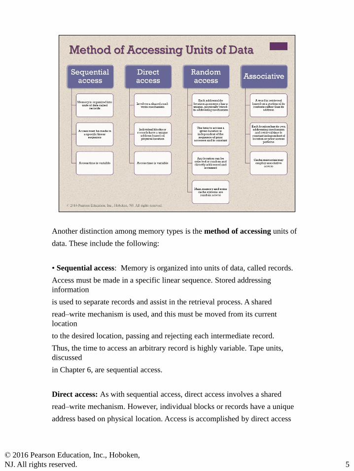
Another distinction among memory types is the method of accessing units of
data. These include the following:
• Sequential access: Memory is organized into units of data, called records.
Access must be made in a specific linear sequence. Stored addressing
information
is used to separate records and assist in the retrieval process. A shared
read–write mechanism is used, and this must be moved from its current
location
to the desired location, passing and rejecting each intermediate record.
Thus, the time to access an arbitrary record is highly variable. Tape units,
discussed
in Chapter 6, are sequential access.
Direct access: As with sequential access, direct access involves a shared
read–write mechanism. However, individual blocks or records have a unique
address based on physical location. Access is accomplished by direct access
© 2016 Pearson Education, Inc., Hoboken,
NJ. All rights reserved.

to reach a general vicinity plus sequential searching, counting, or waiting to
reach the final location. Again, access time is variable. Disk units, discussed in
Chapter 6, are direct access.
• Random access: Each addressable location in memory has a unique, physically
wired-in addressing mechanism. The time to access a given location is independent
of the sequence of prior accesses and is constant. Thus, any location
can be selected at random and directly addressed and accessed. Main memory
and some cache systems are random access.
• Associative: This is a random access type of memory that enables one to make
a comparison of desired bit locations within a word for a specified match, and
to do this for all words simultaneously. Thus, a word is retrieved based on a
portion of its contents rather than its address. As with ordinary random-access
memory, each location has its own addressing mechanism, and retrieval time
is constant independent of location or prior access patterns. Cache memories
may employ associative access.
© 2016 Pearson Education, Inc., Hoboken,
NJ. All rights reserved. 5

6
From a user’s point of view, the two most important characteristics of memory
are capacity and performance. Three performance parameters are used:
• Access time (latency): For random-access memory, this is the time it takes to
perform a read or write operation, that is, the time from the instant that an
address is presented to the memory to the instant that data have been stored
or made available for use. For non-random-access memory, access time is the
time it takes to position the read–write mechanism at the desired location.
• Memory cycle time: This concept is primarily applied to random-access
memory
and consists of the access time plus any additional time required before a
second
access can commence. This additional time may be required for transients to
die
out on signal lines or to regenerate data if they are read destructively. Note that
memory cycle time is concerned with the system bus, not the processor.
© 2016 Pearson Education, Inc., Hoboken,
NJ. All rights reserved.

• Transfer rate: This is the rate at which data can be transferred into or out of a
memory unit. For random-access memory, it is equal to 1/(cycle time).
© 2016 Pearson Education, Inc., Hoboken,
NJ. All rights reserved. 6

A variety of physical types of memory have been employed. The most common
today are semiconductor memory, magnetic surface memory, used for disk and
tape, and optical and magneto-optical.
Several physical characteristics of data storage are important. In a volatile
memory, information decays naturally or is lost when electrical power is switched
off. In a nonvolatile memory, information once recorded remains without deterioration
until deliberately changed; no electrical power is needed to retain information.
Magnetic-surface memories are nonvolatile. Semiconductor memory (memory
on integrated circuits) may be either volatile or nonvolatile. Nonerasable memory
cannot be altered, except by destroying the storage unit. Semiconductor memory of
this type is known as read-only memory (ROM). Of necessity, a practical nonerasable
memory must also be nonvolatile.
For random-access memory, the organization is a key design issue. In this context,
organization refers to the physical arrangement of bits to form words. The
obvious arrangement is not always used, as is explained in Chapter 5.
7
© 2016 Pearson Education, Inc., Hoboken,
NJ. All rights reserved.

The design constraints on a computer’s memory can be summed up by three questions:
How much? How fast? How expensive?
The question of how much is somewhat open ended. If the capacity is there,
applications will likely be developed to use it. The question of how fast is, in a sense,
easier to answer. To achieve greatest performance, the memory must be able to
keep up with the processor. That is, as the processor is executing instructions, we
would not want it to have to pause waiting for instructions or operands. The final
question must also be considered. For a practical system, the cost of memory must
be reasonable in relationship to other components.
As might be expected, there is a trade-off among the three key characteristics
of memory: capacity, access time, and cost. A variety of technologies are used to
implement memory systems, and across this spectrum of technologies, the following
relationships hold:
• Faster access time, greater cost per bit
• Greater capacity, smaller cost per bit
• Greater capacity, slower access time
The dilemma facing the designer is clear. The designer would like to use memory
technologies that provide for large-capacity memory, both because the capacity
8
© 2016 Pearson Education, Inc., Hoboken,
NJ. All rights reserved.
is needed and because the cost per bit is low. However, to meet performance
requirements, the designer needs to use expensive, relatively lower-capacity memories
with short access times.
The way out of this dilemma is not to rely on a single memory component or
technology, but to employ a memory hierarchy.
© 2016 Pearson Education, Inc., Hoboken,
NJ. All rights reserved. 8

A typical hierarchy is illustrated in
Figure 4.1. As one goes down the hierarchy, the following occur:
a. Decreasing cost per bit
b. Increasing capacity
c. Increasing access time
d. Decreasing frequency of access of the memory by the processor
Thus, smaller, more expensive, faster memories are supplemented by larger,
cheaper, slower memories. The key to the success of this organization is item (d)
:decreasing frequency of access. We examine this concept in greater detail when we
discuss the cache, later in this chapter, and virtual memory in Chapter 8. A brief
explanation is provided at this point.
The use of two levels of memory to reduce average access time works in principle,
but only if conditions (a) through (d) apply. By employing a variety of technologies,
a spectrum of memory systems exists that satisfies conditions (a) through
(c). Fortunately, condition (d) is also generally valid.
The basis for the validity of condition (d) is a principle known as locality of
reference [DENN68]. During the course of execution of a program, memory references
by the processor, for both instructions and data, tend to cluster. Programs
typically contain a number of iterative loops and subroutines. Once a loop or subroutine
is entered, there are repeated references to a small set of instructions.
Similarly, operations on tables and arrays involve access to a clustered set of data
words. Over a long period of time, the clusters in use change, but over a short period
of time, the processor is primarily working with fixed clusters of memory references.
9
© 2016 Pearson Education, Inc., Hoboken,
NJ. All rights reserved.
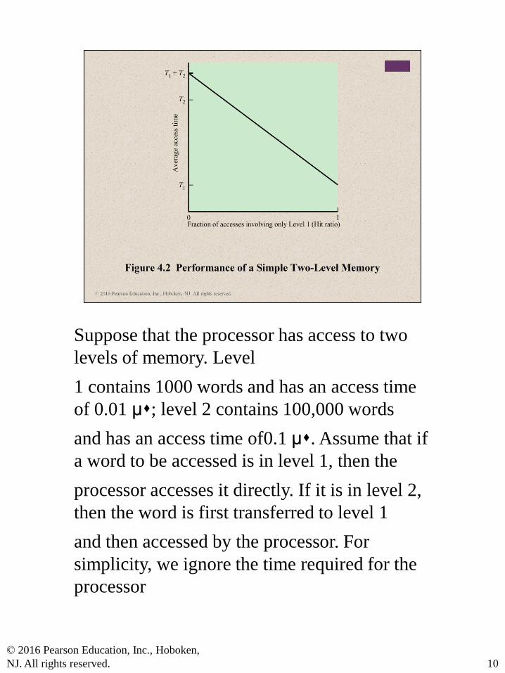
Suppose that the processor has access to two
levels of memory. Level
1 contains 1000 words and has an access time
of 0.01 μs; level 2 contains 100,000 words
and has an access time of0.1 μs. Assume that if
a word to be accessed is in level 1, then the
processor accesses it directly. If it is in level 2,
then the word is first transferred to level 1
and then accessed by the processor. For
simplicity, we ignore the time required for the
processor
10
© 2016 Pearson Education, Inc., Hoboken,
NJ. All rights reserved.
to determine whether the word is in level 1 or level
2. Figure 4.2 shows the general
shape of the curve that covers this situation. The
figure shows the average access time to
a two-level memory as a function of the hit ratio H,
where H is defined as the fraction of
all memory accesses that are found in the faster
memory (e.g., the cache), T1 is the access
time to level 1, and T2 is the access time to level 2.
As can be seen, for high percentages
of level 1 access, the average total access time is
much closer to that of level 1 than that
of level 2.
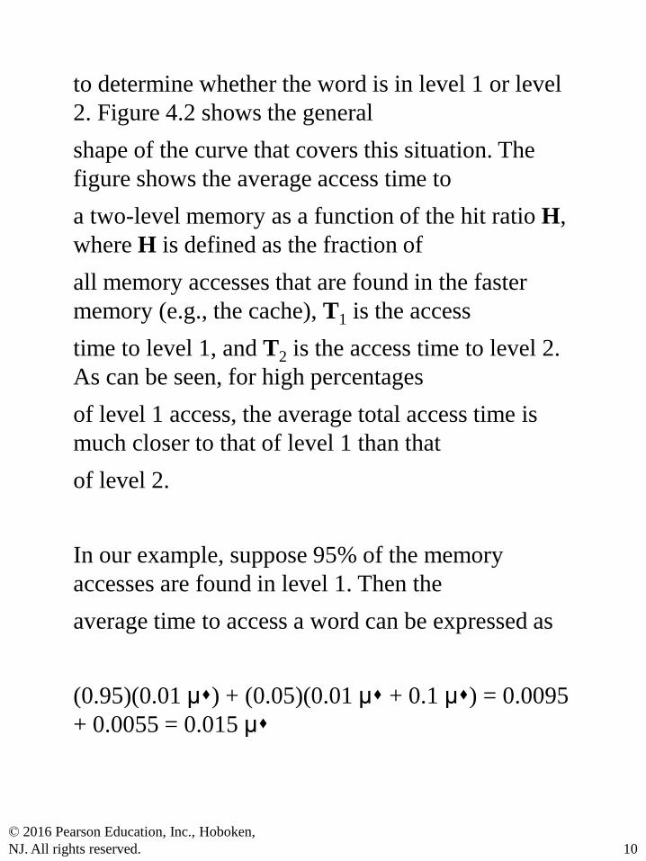
In our example, suppose 95% of the memory
accesses are found in level 1. Then the
average time to access a word can be expressed as
(0.95)(0.01 μs) + (0.05)(0.01 μs + 0.1 μs) = 0.0095
+ 0.0055 = 0.015 μs
© 2016 Pearson Education, Inc., Hoboken,
NJ. All rights reserved. 10

The average access time is much closer to 0.01 μs
than to 0.1 μs, as desired.
Accordingly, it is possible to organize data across
the hierarchy such that the
percentage of accesses to each successively lower
level is substantially less than that
of the level above. Consider the two-level example
already presented. Let level 2
memory contains all program instructions and data.
The current clusters can be
temporarily placed in level 1. From time to time,
one of the clusters in level 1 will
have to be swapped back to level 2 to make room
for a new cluster coming in to
level 1. On average, however, most references will
be to instructions and data contained
in level 1.
This principle can be applied across more than two
levels of memory, as suggested
© 2016 Pearson Education, Inc., Hoboken,
NJ. All rights reserved. 10

by the hierarchy shown in Figure 4.1. The fastest,
smallest, and most expensive
type of memory consists of the registers internal to
the processor. Typically, a
processor will contain a few dozen such registers,
although some machines contain
hundreds of registers. Main memory is the principal
internal memory system of
the computer. Each location in main memory has a
unique address. Main memory
is usually extended with a higher-speed, smaller
cache. The cache is not usually
visible to the programmer or, indeed, to the
processor. It is a device for staging
the movement of data between main memory and
processor registers to improve
performance.
© 2016 Pearson Education, Inc., Hoboken,
NJ. All rights reserved. 10

The three forms of memory just described are, typically, volatile and employ
semiconductor technology. The use of three levels exploits the fact that
semiconductor
memory comes in a variety of types, which differ in speed and cost. Data are
stored more permanently on external mass storage devices, of which the most
common
are hard disk and removable media, such as removable magnetic disk, tape,
and optical storage. External, nonvolatile memory is also referred to as
secondary
memory or auxiliary memory . These are used to store program and data files
and
are usually visible to the programmer only in terms of files and records, as
opposed
to individual bytes or words. Disk is also used to provide an extension to main
memory
known as virtual memory, which is discussed in Chapter 8.
Other forms of memory may be included in the hierarchy. For example, large
11
© 2016 Pearson Education, Inc., Hoboken,
NJ. All rights reserved.

IBM mainframes include a form of internal memory known as expanded storage.
This uses a semiconductor technology that is slower and less expensive than that
of main memory. Strictly speaking, this memory does not fit into the hierarchy but
is a side branch: Data can be moved between main memory and expanded storage
but not between expanded storage and external memory. Other forms of secondary
memory include optical and magneto-optical disks. Finally, additional levels can be
effectively added to the hierarchy in software. A portion of main memory can be
used as a buffer to hold data temporarily that is to be read out to disk. Such a
technique,
sometimes referred to as a disk cache, improves performance in two ways:
■ Disk writes are clustered. Instead of many small transfers of data, we have
a few large transfers of data. This improves disk performance and minimizes
processor involvement.
■ Some data destined for write-out
may be referenced by a program before the
next dump to disk. In that case, the data are retrieved rapidly from the software
cache rather than slowly from the disk.
Appendix 4A examines the performance implications of multilevel memory
structures.
© 2016 Pearson Education, Inc., Hoboken,
NJ. All rights reserved. 11

Cache memory is designed to combine the memory access time of expensive, high-
speed
memory combined with the large memory size of less expensive, lower-speed
memory.
The concept is illustrated in Figure 4.3a. There is a relatively large and slow
main memory together with a smaller, faster cache memory. The cache contains a
copy of portions of main memory. When the processor attempts to read a word of
memory, a check is made to determine if the word is in the cache. If so, the word is
delivered to the processor. If not, a block of main memory, consisting of some fixed
number of words, is read into the cache and then the word is delivered to the
processor.
Because of the phenomenon of locality of reference, when a block of data is
fetched into the cache to satisfy a single memory reference, it is likely that there will
be future references to that same memory location or to other words in the block.
Figure 4.3b depicts the use of multiple levels of cache. The L2 cache is slower
and typically larger than the L1 cache, and the L3 cache is slower and typically
larger than the L2 cache.
12
© 2016 Pearson Education, Inc., Hoboken,
NJ. All rights reserved.

Figure 4.4 depicts the structure of a cache/main-memory system.
13
© 2016 Pearson Education, Inc., Hoboken,
NJ. All rights reserved.
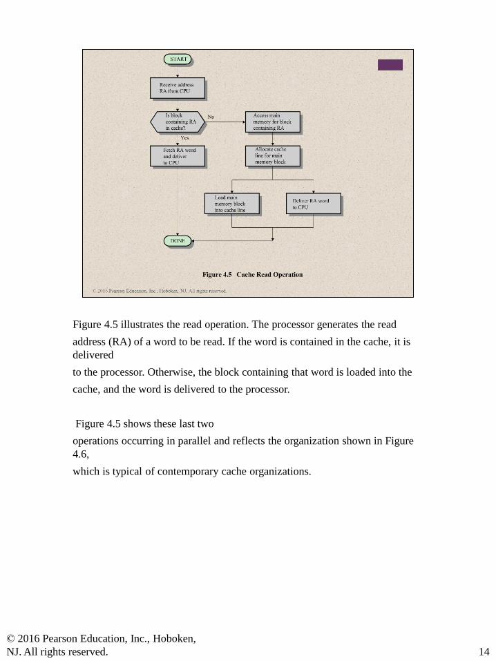
Figure 4.5 illustrates the read operation. The processor generates the read
address (RA) of a word to be read. If the word is contained in the cache, it is
delivered
to the processor. Otherwise, the block containing that word is loaded into the
cache, and the word is delivered to the processor.
Figure 4.5 shows these last two
operations occurring in parallel and reflects the organization shown in Figure
4.6,
which is typical of contemporary cache organizations.
14
© 2016 Pearson Education, Inc., Hoboken,
NJ. All rights reserved.

15
In this organization, the cache
connects to the processor via data, control, and address lines. The data and
address
lines also attach to data and address buffers, which attach to a system bus from
which main memory is reached. When a cache hit occurs, the data and address
buffers
are disabled and communication is only between processor and cache, with no
system bus traffic. When a cache miss occurs, the desired address is loaded
onto the
system bus and the data are returned through the data buffer to both the cache
and
the processor. In other organizations, the cache is physically interposed
between
the processor and the main memory for all data, address, and control lines. In
this
latter case, for a cache miss, the desired word is first read into the cache and
then
transferred from cache to processor.
© 2016 Pearson Education, Inc., Hoboken,
NJ. All rights reserved.

A discussion of the performance parameters related to cache use is contained
in Appendix 4A.
© 2016 Pearson Education, Inc., Hoboken,
NJ. All rights reserved. 15

This section provides an overview of cache design parameters and reports some
typical results. We occasionally refer to the use of caches in high-performance computing
(HPC). HPC deals with supercomputers and their software, especially for
scientific applications that involve large amounts of data, vector and matrix computation,
and the use of parallel algorithms. Cache design for HPC is quite different
than for other hardware platforms and applications. Indeed, many researchers
have found that HPC applications perform poorly on computer architectures that
employ caches [BAIL93]. Other researchers have since shown that a cache hierarchy
can be useful in improving performance if the application software is tuned to
exploit the cache [WANG99, PRES01].
Although there are a large number of cache implementations, there are a few
basic design elements that serve to classify and differentiate cache architectures.
Table 4.2 lists key elements.
16
© 2016 Pearson Education, Inc., Hoboken,
NJ. All rights reserved.
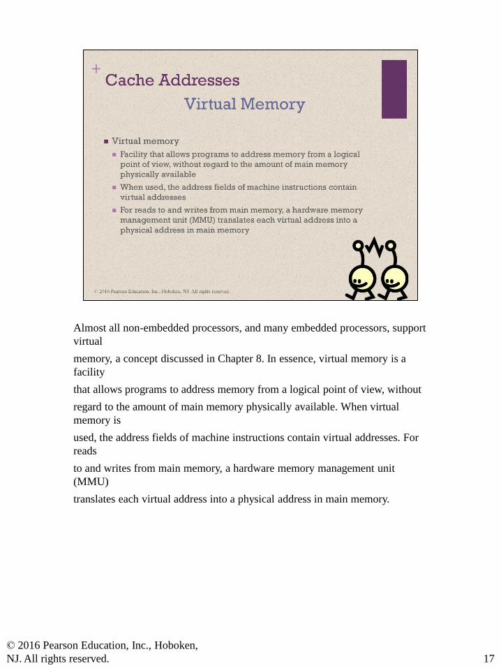
Almost all non-embedded processors, and many embedded processors, support
virtual
memory, a concept discussed in Chapter 8. In essence, virtual memory is a
facility
that allows programs to address memory from a logical point of view, without
regard to the amount of main memory physically available. When virtual
memory is
used, the address fields of machine instructions contain virtual addresses. For
reads
to and writes from main memory, a hardware memory management unit
(MMU)
translates each virtual address into a physical address in main memory.
17
© 2016 Pearson Education, Inc., Hoboken,
NJ. All rights reserved.
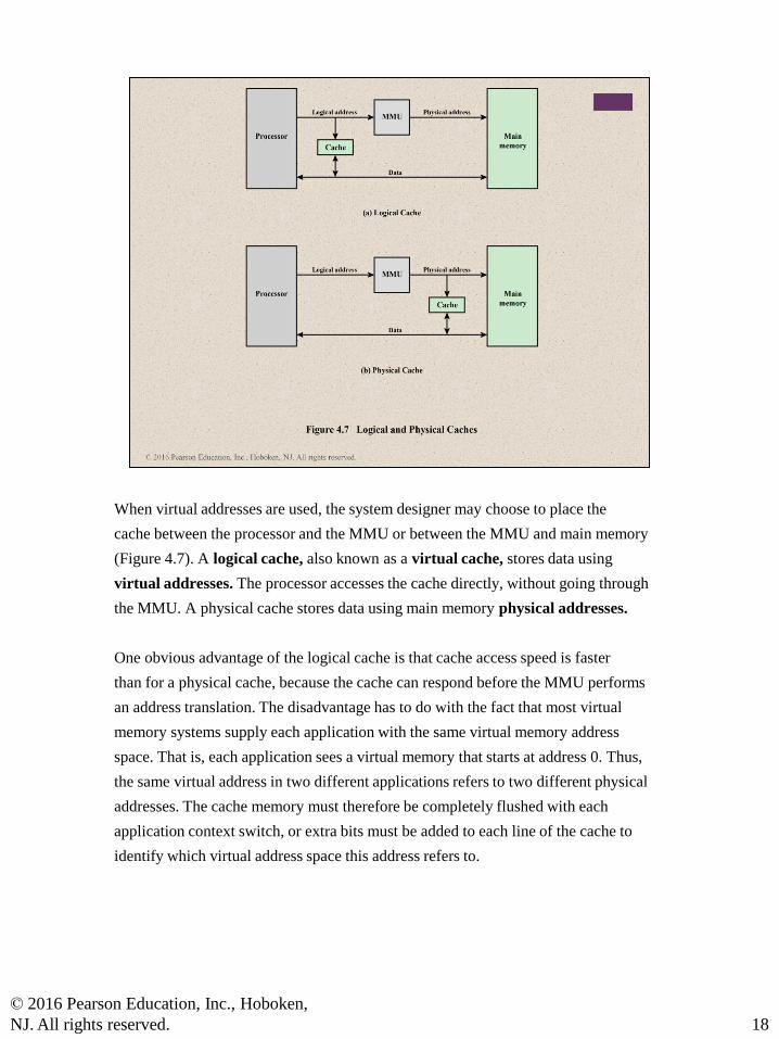
When virtual addresses are used, the system designer may choose to place the
cache between the processor and the MMU or between the MMU and main memory
(Figure 4.7). A logical cache, also known as a virtual cache, stores data using
virtual addresses. The processor accesses the cache directly, without going through
the MMU. A physical cache stores data using main memory physical addresses.
One obvious advantage of the logical cache is that cache access speed is faster
than for a physical cache, because the cache can respond before the MMU performs
an address translation. The disadvantage has to do with the fact that most virtual
memory systems supply each application with the same virtual memory address
space. That is, each application sees a virtual memory that starts at address 0. Thus,
the same virtual address in two different applications refers to two different physical
addresses. The cache memory must therefore be completely flushed with each
application context switch, or extra bits must be added to each line of the cache to
identify which virtual address space this address refers to.
18
© 2016 Pearson Education, Inc., Hoboken,
NJ. All rights reserved.

The first item in Table 4.2, cache size, has already been discussed. We would like the
size of the cache to be small enough so that the overall average cost per bit is close
to that of main memory alone and large enough so that the overall average access
time is close to that of the cache alone. There are several other motivations for
minimizing cache size. The larger the cache, the larger the number of gates involved
in addressing the cache. The result is that large caches tend to be slightly slower
than small ones—even when built with the same integrated circuit technology and
put in the same place on chip and circuit board. The available chip and board area
also limits cache size. Because the performance of the cache is very sensitive to the
nature of the workload, it is impossible to arrive at a single “optimum” cache size.
Table 4.3 lists the cache sizes of some current and past processors.
19
© 2016 Pearson Education, Inc., Hoboken,
NJ. All rights reserved.

20
Because there are fewer cache lines than main memory blocks, an algorithm is
needed for mapping main memory blocks into cache lines. Further, a means is
needed for determining which main memory block currently occupies a cache
line.
The choice of the mapping function dictates how the cache is organized. Three
techniques can be used: direct, associative, and set associative.
Direct mapping: The simplest technique, known as direct mapping, maps
each
block of main memory into only one possible cache line.
Associative mapping: Associative mapping overcomes the disadvantage of
direct
mapping by permitting each main memory block to be loaded into any line of
the
cache.
Set-associative mapping: Set-associative mapping is a compromise that
© 2016 Pearson Education, Inc., Hoboken,
NJ. All rights reserved.

exhibits the strengths of both the direct and associative approaches while reducing
their disadvantages.
© 2016 Pearson Education, Inc., Hoboken,
NJ. All rights reserved. 20

21
The mapping is expressed as
i = j modulo m
where
i = cache line number
j = main memory block number
m = number of lines in the cache
Figure 4.8a shows the mapping for the first m blocks of main memory. Each
block of main memory maps into one unique line of the cache. The next m
blocks
of main memory map into the cache in the same fashion; that is, block Bm of main
memory maps into line L0 of cache, block Bm+1 maps into line L1, and so on.
© 2016 Pearson Education, Inc., Hoboken,
NJ. All rights reserved.

22
The mapping function is easily implemented using the main memory address.
Figure 4.9 illustrates the general mechanism.
For purposes of cache access, each
main memory address can be viewed as consisting of three fields. The least
significant
w bits identify a unique word or byte within a block of main memory; in most
contemporary machines, the address is at the byte level. The remaining s bits
specify
one of the 2s blocks of main memory. The cache logic interprets these s bits
as
a tag of s - r bits (most significant portion) and a line field of r bits. This latter
field
identifies one of the m = 2r lines of the cache. To summarize,
■ Address length = (s + w ) bits
■ Number of addressable units = 2s+w words or bytes
© 2016 Pearson Education, Inc., Hoboken,
NJ. All rights reserved.

■ Block size = line size = 2w words or bytes
■ Number of blocks in main memory = 2s+w/2w = 2s
■ Number of lines in cache = m = 2r
■ Size of cache = 2r+w words or bytes
■ Size of tag = (s - r ) bits
© 2016 Pearson Education, Inc., Hoboken,
NJ. All rights reserved. 22

Figure 4.10 shows our example system using direct mapping. In the example,
m = 16K = 214 and i = j modulo 214. The mapping becomes
Cache Line Starting Memory Address of Block
0 000000, 010000, …, FF0000
1 000004, 010004, …, FF0004
. .
. .
. .
214 - 1 00FFFC, 01FFFC, …, FFFFFC
Note that no two blocks that map into the same line number have the same tag
number. Thus,
blocks with starting addresses 000000, 010000, …, FF0000 have tag numbers
00, 01, …, FF, respectively.
Referring back to Figure 4.5, a read operation works as follows. The cache
23
© 2016 Pearson Education, Inc., Hoboken,
NJ. All rights reserved.

system is presented
with a 24-bit address. The 14-bit line number is used as an index into the cache to
access a particular
line. If the 8-bit tag number matches the tag number currently stored in that line, then
the 2-bit word
number is used to select one of the 4 bytes in that line. Otherwise, the 22-bit tag-plus-
line
field is used to fetch a block from main memory. The actual address that is used for
the fetch is the 22-bit
tag-plus-line concatenated with two 0 bits, so that 4 bytes are fetched starting on a
block boundary.
The effect of this mapping is that blocks of main memory are assigned to lines
of the cache as follows:
Cache line Main memory blocks assigned
0 0, m, 2m, c, 2s - m
1 1, m + 1, 2m + 1, c, 2s - m + 1
. .
. .
. .
m - 1 m - 1, 2m - 1, 3m - 1, c, 2s - 1
Thus, the use of a portion of the address as a line number provides a unique
mapping of each block of main memory into the cache. When a block is actually
read into its assigned line, it is necessary to tag the data to distinguish it from other
blocks that can fit into that line. The most significant s - r bits serve this purpose.
© 2016 Pearson Education, Inc., Hoboken,
NJ. All rights reserved. 23

The direct mapping technique is simple and inexpensive to implement. Its
main disadvantage is that there is a fixed cache location for any given block.
Thus,
if a program happens to reference words repeatedly from two different blocks
that
map into the same line, then the blocks will be continually swapped in the
cache,
and the hit ratio will be low (a phenomenon known as thrashing).
24
© 2016 Pearson Education, Inc., Hoboken,
NJ. All rights reserved.

One approach to lower the miss penalty is to remember what was discarded
in case it is needed again. Since the discarded data has already been fetched, it
can
be used again at a small cost. Such recycling is possible using a victim cache.
Victim
cache was originally proposed as an approach to reduce the conflict misses of
direct
mapped caches without affecting its fast access time. Victim cache is a fully
associative
cache, whose size is typically 4 to 16 cache lines, residing between a direct
mapped L1
cache and the next level of memory. This concept is explored in Appendix F.
25
© 2016 Pearson Education, Inc., Hoboken,
NJ. All rights reserved.

26
Associative mapping overcomes the disadvantage of direct
mapping by permitting each main memory block to be loaded into any line of
the
cache (Figure 4.8b). In this case, the cache control logic interprets a memory
address
simply as a Tag and a Word field. The Tag field uniquely identifies a block of
main
memory. To determine whether a block is in the cache, the cache control logic
must
simultaneously examine every line’s tag for a match. Figure 4.11 illustrates the
logic.
© 2016 Pearson Education, Inc., Hoboken,
NJ. All rights reserved.
27
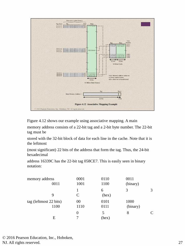
Figure 4.12 shows our example using associative mapping. A main
memory address consists of a 22-bit tag and a 2-bit byte number. The 22-bit
tag must be
stored with the 32-bit block of data for each line in the cache. Note that it is
the leftmost
(most significant) 22 bits of the address that form the tag. Thus, the 24-bit
hexadecimal
address 16339C has the 22-bit tag 058CE7. This is easily seen in binary
notation:
memory address 0001 0110 0011
0011 1001 1100 (binary)
1 6 3 3
9 C (hex)
tag (leftmost 22 bits) 00 0101 1000
1100 1110 0111 (binary)
0 5 8 C
E 7 (hex)
© 2016 Pearson Education, Inc., Hoboken,
NJ. All rights reserved.

With associative mapping, there is flexibility as to which block to replace
when
a new block is read into the cache. Replacement algorithms, discussed later in
this
section, are designed to maximize the hit ratio. The principal disadvantage of
associative
mapping is the complex circuitry required to examine the tags of all cache
lines in parallel.
28
© 2016 Pearson Education, Inc., Hoboken,
NJ. All rights reserved.

29
Set-associative mapping is a compromise that
exhibits the strengths of both the direct and associative approaches while
reducing
their disadvantages.
In this case, the cache consists of a number sets, each of which consists of a
number of lines. The relationships are
m = v* k
i = j modulo v
where
i = cache set number
j = main memory block number
© 2016 Pearson Education, Inc., Hoboken,
NJ. All rights reserved.
m = number of lines in the cache
v = number of sets
k = number of lines in each set
This is referred to as k-way set-associative mapping. With set-associative
mapping,block Bj can be mapped into any of the lines of set j.
© 2016 Pearson Education, Inc., Hoboken,
NJ. All rights reserved. 29

Figure 4.13a illustrates
this mapping for the first v blocks of main memory. As with associative mapping,
each word maps into multiple cache lines. For set-associative mapping, each word
maps into all the cache lines in a specific set, so that main memory block B0 maps
into set 0, and so on. Thus, the set-associative cache can be physically implemented
as n associative caches. It is also possible to implement the set-associative cache as
k direct mapping caches, as shown in Figure 4.13b. Each direct-mapped cache is
referred to as a way, consisting of v lines. The first v lines of main memory are direct
mapped into the v lines of each way; the next group of v lines of main memory are
similarly mapped, and so on. The direct-mapped implementation is typically used
for small degrees of associativity (small values of k) while the associative-mapped
implementation is typically used for higher degrees of associativity [JACO08].
30
© 2016 Pearson Education, Inc., Hoboken,
NJ. All rights reserved.
31
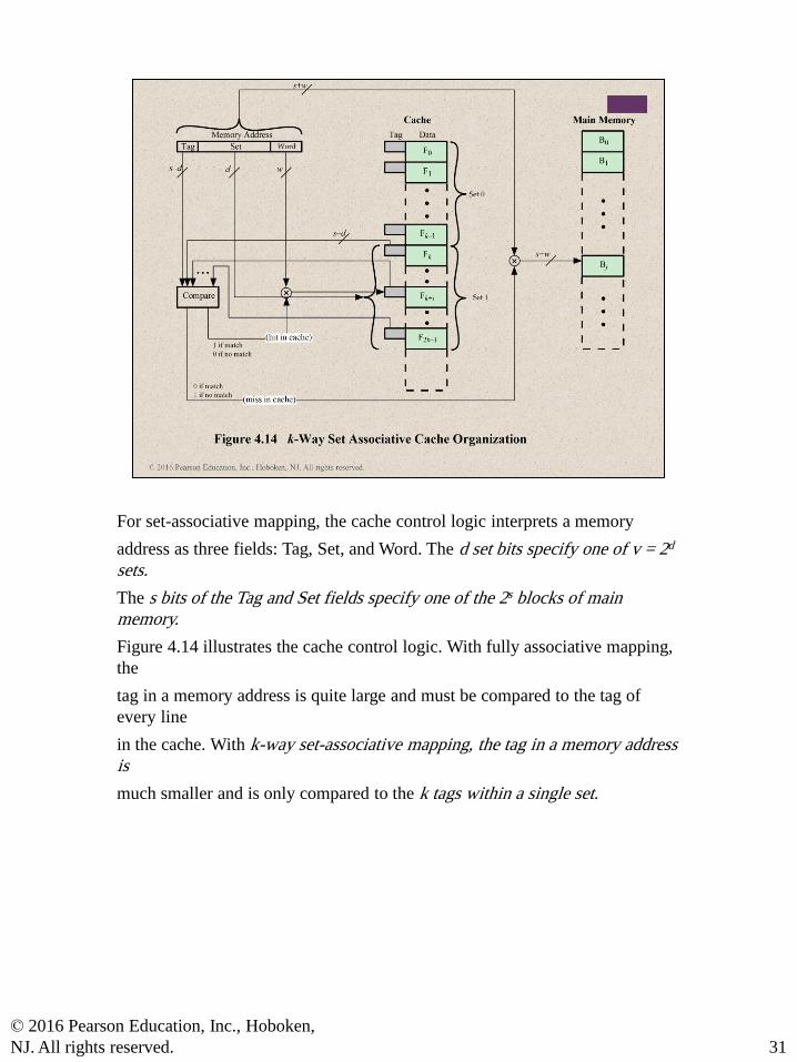
For set-associative mapping, the cache control logic interprets a memory
address as three fields: Tag, Set, and Word. The d set bits specify one of v = 2d
sets.
The s bits of the Tag and Set fields specify one of the 2s blocks of main
memory.
Figure 4.14 illustrates the cache control logic. With fully associative mapping,
the
tag in a memory address is quite large and must be compared to the tag of
every line
in the cache. With k-way set-associative mapping, the tag in a memory address
is
much smaller and is only compared to the k tags within a single set.
© 2016 Pearson Education, Inc., Hoboken,
NJ. All rights reserved.

Set Associative Mapping Summary.
32
© 2016 Pearson Education, Inc., Hoboken,
NJ. All rights reserved.
33
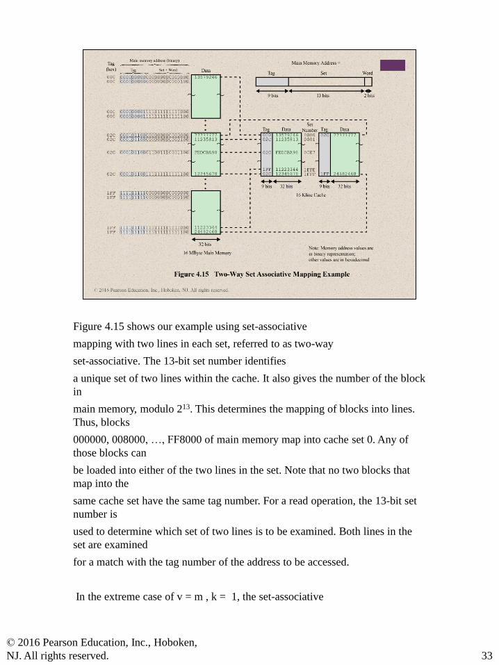
Figure 4.15 shows our example using set-associative
mapping with two lines in each set, referred to as two-way
set-associative. The 13-bit set number identifies
a unique set of two lines within the cache. It also gives the number of the block
in
main memory, modulo 213. This determines the mapping of blocks into lines.
Thus, blocks
000000, 008000, …, FF8000 of main memory map into cache set 0. Any of
those blocks can
be loaded into either of the two lines in the set. Note that no two blocks that
map into the
same cache set have the same tag number. For a read operation, the 13-bit set
number is
used to determine which set of two lines is to be examined. Both lines in the
set are examined
for a match with the tag number of the address to be accessed.
In the extreme case of v = m , k = 1, the set-associative
© 2016 Pearson Education, Inc., Hoboken,
NJ. All rights reserved.

technique reduces to direct mapping, and for v = 1, k = m , it reduces to associative
mapping. The use of
two lines per set (v = m /2, k = 2) is the most common set-associative
organization. It significantly improves the hit ratio over direct mapping. Four- way set
associative
(v = m /4, k = 4) makes a modest additional improvement for a relatively small
additional cost [MAYB84, HILL89]. Further increases in the number of lines per
set have little effect.
© 2016 Pearson Education, Inc., Hoboken,
NJ. All rights reserved. 33

Figure 4.16 shows the results of one simulation study of set-associative cache
performance as a function of cache size [GENU04]. The difference in performance
between direct and two-way set associative is significant up to at least a cache size of
64 kB. Note also that the difference between two-way and four-way at 4 kB is much
less than the difference in going from for 4 kB to 8 kB in cache size. The complexity
of the cache increases in proportion to the associativity, and in this case would not
be justifiable against increasing cache size to 8 or even 16 Kbytes. A final point to
note is that beyond about 32 kB, increase in cache size brings no significant increase
in performance.
The results of Figure 4.16 are based on simulating the execution of a GCC
compiler. Different applications may yield different results. For example, [CANT01]
reports on the results for cache performance using many of the CPU2000 SPEC
benchmarks. The results of [CANT01] in comparing hit ratio to cache size follow
the same pattern as Figure 4.16, but the specific values are somewhat different.
34
© 2016 Pearson Education, Inc., Hoboken,
NJ. All rights reserved.

35
Once the cache has been filled, when a new block is brought into the cache,
one
of the existing blocks must be replaced. For direct mapping, there is only one
possible
line for any particular block, and no choice is possible. For the associative
and set-associative techniques, a replacement algorithm is needed. To achieve
high
speed, such an algorithm must be implemented in hardware.
© 2016 Pearson Education, Inc., Hoboken,
NJ. All rights reserved.

36
A number of algorithms
have been tried. We mention four of the most common. Probably the most
effective is least recently used (LRU): Replace that block in the set that has
been in
the cache longest with no reference to it. For two-way set associative, this is
easily
implemented. Each line includes a USE bit. When a line is referenced, its USE
bit
is set to 1 and the USE bit of the other line in that set is set to 0. When a block
is to
be read into the set, the line whose USE bit is 0 is used. Because we are
assuming
that more recently used memory locations are more likely to be referenced,
LRU
should give the best hit ratio. LRU is also relatively easy to implement for a
fully
associative cache. The cache mechanism maintains a separate list of indexes to
all
© 2016 Pearson Education, Inc., Hoboken,
NJ. All rights reserved.
the lines in the cache. When a line is referenced, it moves to the front of the list.
For replacement, the line at the back of the list is used. Because of its simplicity of
implementation, LRU is the most popular replacement algorithm.
Another possibility is first-in-first-out (FIFO): Replace that block in the set
that has been in the cache longest. FIFO is easily implemented as a round-robin
or circular buffer technique. Still another possibility is least frequently used (LFU):
Replace that block in the set that has experienced the fewest references. LFU could
be implemented by associating a counter with each line. A technique not based on
usage (i.e., not LRU, LFU, FIFO, or some variant) is to pick a line at random from
among the candidate lines. Simulation studies have shown that random replacement
provides only slightly inferior performance to an algorithm based on usage [SMIT82].
© 2016 Pearson Education, Inc., Hoboken,
NJ. All rights reserved. 36

37
When a block that is resident in the cache is to be replaced, there are two cases
to
consider. If the old block in the cache has not been altered, then it may be
overwritten
with a new block without first writing out the old block. If at least one write
operation has been performed on a word in that line of the cache, then main
memory
must be updated by writing the line of cache out to the block of memory
before
bringing in the new block. A variety of write policies, with performance and
economic
trade-offs, is possible. There are two problems to contend with. First, more
than one device may have access to main memory. For example, an I/O
module
may be able to read-write directly to memory. If a word has been altered only
in the
cache, then the corresponding memory word is invalid. Further, if the I/O
device
© 2016 Pearson Education, Inc., Hoboken,
NJ. All rights reserved.

has altered main memory, then the cache word is invalid. A more complex problem
occurs when multiple processors are attached to the same bus and each processor
has its own local cache. Then, if a word is altered in one cache, it could conceivably
invalidate a word in other caches.
© 2016 Pearson Education, Inc., Hoboken,
NJ. All rights reserved. 37

38
The simplest technique is called write through. Using this technique, all write
operations are made to main memory as well as to the cache, ensuring that
main
memory is always valid. Any other processor–cache module can monitor
traffic to
main memory to maintain consistency within its own cache. The main
disadvantage
of this technique is that it generates substantial memory traffic and may create
a bottleneck.
An alternative technique, known as write back, minimizes memory writes.
With write back, updates are made only in the cache. When an update occurs, a
dirty bit, or use bit, associated with the line is set. Then, when a block is
replaced, it
is written back to main memory if and only if the dirty bit is set. The problem
with
write back is that portions of main memory are invalid, and hence accesses by
I/O
modules can be allowed only through the cache. This makes for complex
© 2016 Pearson Education, Inc., Hoboken,
NJ. All rights reserved.

circuitry
and a potential bottleneck. Experience has shown that the percentage of memory
references that are writes is on the order of 15% [SMIT82]. However, for HPC
applications, this number may approach 33% (vector-vector multiplication) and can
go as high as 50% (matrix transposition).
In a bus organization in which more than one device (typically a processor)
has a cache and main memory is shared, a new problem is introduced. If data in one
cache are altered, this invalidates not only the corresponding word in main memory,
but also that same word in other caches (if any other cache happens to have that
same word). Even if a write-through policy is used, the other caches may contain
invalid data. A system that prevents this problem is said to maintain cache coherency.
Possible approaches to cache coherency include the following:
• Bus watching with write through: Each cache controller monitors the address
lines to detect write operations to memory by other bus masters. If another
master writes to a location in shared memory that also resides in the cache
memory, the cache controller invalidates that cache entry. This strategy depends
on the use of a write-through policy by all cache controllers.
• Hardware transparency: Additional hardware is used to ensure that all updates
to main memory via cache are reflected in all caches. Thus, if one processor
modifies a word in its cache, this update is written to main memory. In addition,
any matching words in other caches are similarly updated.
• Non-cacheable memory: Only a portion of main memory is shared by more
than one processor, and this is designated as non-cacheable. In such a system,
all accesses to shared memory are cache misses, because the shared memory
is never copied into the cache. The non-cacheable memory can be identified
using chip-select logic or high-address bits.
© 2016 Pearson Education, Inc., Hoboken,
NJ. All rights reserved. 38

Another design element is the line size. When a block of data is retrieved and placed
in the cache, not only the desired word but also some number of adjacent words are
retrieved. As the block size increases from very small to larger sizes, the hit ratio
will at first increase because of the principle of locality, which states that data in the
vicinity of a referenced word are likely to be referenced in the near future. As the
block size increases, more useful data are brought into the cache. The hit ratio will
begin to decrease, however, as the block becomes even bigger and the probability
of using the newly fetched information becomes less than the probability of reusing
the information that has to be replaced. Two specific effects come into play:
• Larger blocks reduce the number of blocks that fit into a cache. Because each
block fetch overwrites older cache contents, a small number of blocks results
in data being overwritten shortly after they are fetched.
• As a block becomes larger, each additional word is farther from the requested
word and therefore less likely to be needed in the near future.
The relationship between block size and hit ratio is complex, depending on
the locality characteristics of a particular program, and no definitive optimum value
has been found. A size of from 8 to 64 bytes seems reasonably close to optimum
39
© 2016 Pearson Education, Inc., Hoboken,
NJ. All rights reserved.

[SMIT87, PRZY88, PRZY90, HAND98]. For HPC systems, 64- and 128-byte cache
line sizes are most frequently used.
© 2016 Pearson Education, Inc., Hoboken,
NJ. All rights reserved. 39

As logic density has increased, it has become possible to
have a cache on the same chip as the processor: the on-chip cache. Compared with
a cache reachable via an external bus, the on-chip cache reduces the processor’s
external bus activity and therefore speeds up execution times and increases overall
system performance. When the requested instruction or data is found in the on-chip
cache, the bus access is eliminated. Because of the short data paths internal to
the processor, compared with bus lengths, on-chip cache accesses will complete
appreciably faster than would even zero-wait state bus cycles. Furthermore, during
this period the bus is free to support other transfers.
The inclusion of an on-chip cache leaves open the question of whether an
off-chip, or external, cache is still desirable. Typically, the answer is yes, and most
contemporary
designs include both on-chip and external caches. The simplest such organization
is known as a two-level cache, with the internal cache designated as level 1 (L1)
and the external cache designated as level 2 (L2). The reason for including an L2
cache
is the following: If there is no L2 cache and the processor makes an access request
for a memory location not in the L1 cache, then the processor must access DRAM or
40
© 2016 Pearson Education, Inc., Hoboken,
NJ. All rights reserved.

ROM memory across the bus. Due to the typically slow bus speed and slow memory
access time, this results in poor performance. On the other hand, if an L2 SRAM
(static
RAM) cache is used, then frequently the missing information can be quickly retrieved.
If the SRAM is fast enough to match the bus speed, then the data can be accessed
using a zero-wait state transaction, the fastest type of bus transfer.
Two features of contemporary cache design for multilevel caches are noteworthy.
First, for an off-chip L2 cache, many designs do not use the system bus as
the path for transfer between the L2 cache and the processor, but use a separate
data path, so as to reduce the burden on the system bus. Second, with the continued
shrinkage of processor components, a number of processors now incorporate the L2
cache on the processor chip, improving performance.
The potential savings due to the use of an L2 cache depends on the hit rates
in both the L1 and L2 caches. Several studies have shown that, in general, the use
of a second-level cache does improve performance (e.g., see [AZIM92], [NOVI93],
[HAND98]). However, the use of multilevel caches does complicate all of the design
issues related to caches, including size, replacement algorithm, and write policy; see
[HAND98] and [PEIR99] for discussions.
© 2016 Pearson Education, Inc., Hoboken,
NJ. All rights reserved. 40
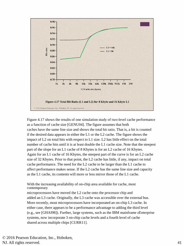
Figure 4.17 shows the results of one simulation study of two-level cache performance
as a function of cache size [GENU04]. The figure assumes that both
caches have the same line size and shows the total hit ratio. That is, a hit is counted
if the desired data appears in either the L1 or the L2 cache. The figure shows the
impact of L2 on total hits with respect to L1 size. L2 has little effect on the total
number of cache hits until it is at least double the L1 cache size. Note that the steepest
part of the slope for an L1 cache of 8 Kbytes is for an L2 cache of 16 Kbytes.
Again for an L1 cache of 16 Kbytes, the steepest part of the curve is for an L2 cache
size of 32 Kbytes. Prior to that point, the L2 cache has little, if any, impact on total
cache performance. The need for the L2 cache to be larger than the L1 cache to
affect performance makes sense. If the L2 cache has the same line size and capacity
as the L1 cache, its contents will more or less mirror those of the L1 cache.
With the increasing availability of on-chip area available for cache, most contemporary
microprocessors have moved the L2 cache onto the processor chip and
added an L3 cache. Originally, the L3 cache was accessible over the external bus.
More recently, most microprocessors have incorporated an on-chip L3 cache. In
either case, there appears to be a performance advantage to adding the third level
(e.g., see [GHAI98]). Further, large systems, such as the IBM mainframe zEnterprise
systems, now incorporate 3 on-chip cache levels and a fourth level of cache
shared across multiple chips [CURR11].
41
© 2016 Pearson Education, Inc., Hoboken,
NJ. All rights reserved.

When the on-chip cache first made an appearance,
many of the designs consisted of a single cache used to store references to both data
and instructions. More recently, it has become common to split the cache into two:
one dedicated to instructions and one dedicated to data. These two caches both exist
at the same level, typically as two L1 caches. When the processor attempts to fetch an
instruction from main memory, it first consults the instruction L1 cache, and when the
processor attempts to fetch data from main memory, it first consults the data L1 cache.
There are two potential advantages of a unified cache:
• For a given cache size, a unified cache has a higher hit rate than split caches
because it balances the load between instruction and data fetches automatically.
That is, if an execution pattern involves many more instruction fetches
than data fetches, then the cache will tend to fill up with instructions, and if an
execution pattern involves relatively more data fetches, the opposite will occur.
• Only one cache needs to be designed and implemented.
The trend is toward split caches at the L1 and unified caches for higher levels,
particularly for superscalar machines, which emphasize parallel instruction execution
and the prefetching of predicted future instructions. The key advantage of the
split cache design is that it eliminates contention for the cache between the instruction
fetch/decode unit and the execution unit. This is important in any design that
relies on the pipelining of instructions. Typically, the processor will fetch instructions
ahead of time and fill a buffer, or pipeline, with instructions to be executed. Suppose
now that we have a unified instruction/data cache. When the execution unit performs
a memory access to load and store data, the request is submitted to the unified cache.
If, at the same time, the instruction prefetcher issues a read request to the cache for
an instruction, that request will be temporarily blocked so that the cache can service
the execution unit first, enabling it to complete the currently executing instruction.
42
© 2016 Pearson Education, Inc., Hoboken,
NJ. All rights reserved.

This cache contention can degrade performance by interfering with efficient use of
the instruction pipeline. The split cache structure overcomes this difficulty.
© 2016 Pearson Education, Inc., Hoboken,
NJ. All rights reserved. 42

43
The evolution of cache organization is seen clearly in the evolution of Intel
microprocessors
(Table 4.4). The 80386 does not include an on-chip cache. The 80486
includes a single on-chip cache of 8 Kbytes, using a line size of 16 bytes and a
four-way set-associative organization. All of the Pentium processors include
two
on-chip L1 caches, one for data and one for instructions. For the Pentium 4,
the
L1 data cache is 16 Kbytes, using a line size of 64 bytes and a four-way set-
associative
organization. The Pentium 4 instruction cache is described subsequently. The
Pentium II also includes an L2 cache that feeds both of the L1 caches. The L2
cache
is eight-way set associative with a size of 512 kB and a line size of 128 bytes.
An L3
cache was added for the Pentium III and became on-chip with high-end
versions of
the Pentium 4.
© 2016 Pearson Education, Inc., Hoboken,
NJ. All rights reserved.

Figure 4.18 provides a simplified view of the Pentium 4 organization, highlighting
the placement of the three caches. The processor core consists of four major
components:
• Fetch/decode unit: Fetches program instructions in order from the L2 cache,
decodes these into a series of micro-operations, and stores the results in the L1
instruction cache.
• Out-of-order execution logic: Schedules execution of the micro-operations
subject to data dependencies and resource availability; thus, micro-operations
may be scheduled for execution in a different order than they were fetched
from the instruction stream. As time permits, this unit schedules speculative
execution of micro-operations that may be required in the future.
Execution units: These units executes micro-operations, fetching the required
data from the L1 data cache and temporarily storing results in registers.
• Memory subsystem: This unit includes the L2 and L3 caches and the system
bus, which is used to access main memory when the L1 and L2 caches have a
cache miss and to access the system I/O resources.
Unlike the organization used in all previous Pentium models, and in most
other processors, the Pentium 4 instruction cache sits between the instruction
decode logic and the execution core. The reasoning behind this design decision is
as follows: As discussed more fully in Chapter 16, the Pentium process decodes, or
translates, Pentium machine instructions into simple RISC-like instructions called
micro-operations. The use of simple, fixed-length micro-operations enables the use
of superscalar pipelining and scheduling techniques that enhance performance.
However, the Pentium machine instructions are cumbersome to decode; they have a
variable number of bytes and many different options. It turns out that performance
is enhanced if this decoding is done independently of the scheduling and pipelining
logic. We return to this topic in Chapter 16.
The data cache employs a write-back policy: Data are written to main memory
44
© 2016 Pearson Education, Inc., Hoboken,
NJ. All rights reserved.

only when they are removed from the cache and there has been an update. The
Pentium 4 processor can be dynamically configured to support write-through caching.
© 2016 Pearson Education, Inc., Hoboken,
NJ. All rights reserved. 44

The L1 data cache is controlled by two bits in one of the control registers,
labeled the CD (cache disable) and NW (not write-through) bits (Table 4.5).
There
are also two Pentium 4 instructions that can be used to control the data cache:
INVD
invalidates (flushes) the internal cache memory and signals the external cache
(if
any) to invalidate. WBINVD writes back and invalidates internal cache and
then
writes back and invalidates external cache.
Both the L2 and L3 caches are eight-way set-associative with a line size of
128 bytes.
45
© 2016 Pearson Education, Inc., Hoboken,
NJ. All rights reserved.

46
Chapter 4 summary.
© 2016 Pearson Education, Inc., Hoboken,
NJ. All rights reserved.