1111111111111111111inuun1111111111u~ - nasa · include, inter alia, insertion loss, return loss,...
TRANSCRIPT
1111111111111111111inuun1111111111u~(12) United States Patent
Shu et al.
(54) COUPLING INDUCTOR BASED HYBRIDMILLIMETER-WAVE SWITCH
(71) Applicant: The Regents of the University ofCalifornia, Oakland, CA (US)
(72) Inventors: Ran Shu, Davis, CA (US); Adrian J.Tang, Davis, CA (US); Qun Gu, Davis,CA (US); Brian J. Drouin, Davis, CA(US)
(73) Assignees: THE REGENTS OF THEUNIVERSITY OF CALIFORNIA,Oakland, CA (US); CALIFORNIAINSTITUTE OF TECHNOLOGY,Pasadena, CA (US)
(*) Notice: Subject to any disclaimer, the term of thispatent is extended or adjusted under 35U.S.C. 154(b) by 0 days.
(21) Appl. No.: 15/154,813
(22) Filed: May 13, 2016
(65) Prior Publication Data
US 2016/0336934 Al Nov. 17, 2016
Related U.S. Application Data
(60) Provisional application No. 62/161,822, filed on May14, 2015.
(51) Int. Cl.H03K 17/10 (2006.01)
(io) Patent No.: US 9,621,152 B2(45) Date of Patent: Apr. 11, 2017
(52) U.S. Cl.CPC .................................. H03K 17/102 (2013.01)
(58) Field of Classification SearchCPC .................................................... H03K 17/102See application file for complete search history.
(56) References Cited
U.S. PATENT DOCUMENTS
5,717,356 A * 2/1998 Kohama .............. H03K 17/063327/365
6,201,455 131 * 3/2001 Kusunoki ................. HO11' 1/15327/308
20 14/03 2749 5 Al * 11/2014 He ........................... HO1H 9/54333/103
* cited by examiner
Primary Examiner Hai L Nguyen(74) Attorney, Agent, or Firm Park, Vaughan, Fleming& Dowler LLP; Laxman Sahasrabuddhe
(57) ABSTRACT
A switch comprising a plurality of inductors and a pluralityof shunt transistors is described. Each inductor can beelectrically coupled between adjacent shunt transistors toform a distributed switch structure. At least two inductors inthe plurality of inductors can be inductively coupled witheach other. The plurality of inductors can correspond toportions of a coupling inductor, wherein the coupling induc-tor can have an irregular octagonal shape.
OW
20 Claims, 5 Drawing Sheets
408 y
402 1 404In 10 Out
Mf 2 400Mfr# e and
V VA rl R2 ' ' R,5 R&9M ..
https://ntrs.nasa.gov/search.jsp?R=20170004328 2018-06-09T14:58:26+00:00Z

U.S. Patent
P1
Apr. 11, 2017 Sheet 1 of 5 US 9,621,152 B2
n stages
wss ••r P2
r oAA(-4 o-YM oAm4ctd Ti Vctrf T2 Vctrl To., ctrt Tn
I
-40`~aew
-4
m -5000 _5j
FIG.1(PRIOR ART)
R,m 1oP10101
Sao, 'ii..fF{cs;ttrn=
n
"~
= ~
n 4̂
40 50 80 70 80 90Frequency (GHz)
FIG. 2A
m
7% 7% n=2i
n= +Lp
'Y~f "off
Yn=4 f
40 50 00 70 80 00Frequency GHz
FIG. 2B

U.S. Patent Apr. 11, 2017 Sheet 2 of 5 US 9,621,152 B2
.:- l .
2 02
FIG. 3B
R
FIG. 3C
Ez

U.S. Patent Apr. 11, 2017 Sheet 3 of 5 US 9,621,152 B2
VC
~3
21
404
406 M3f3
R4 RS
FIG. 4
2
11-0 Out
R6
-Sub S G D B D-:III
FIG. 5A
U.S. Patent Apr. 11, 2017 Sheet 4 of 5 US 9,621,152 B2
ctrl Substrate Network
Bulk I NNW I P-subiI DIDLdd
2 I D3 I Rsubrds Cds
hm.J LA
s T c-A is lOkO IOW
ADD
s
U.S. Patent Apr. 11, 2017 Sheet 5 of 5 US 9,621,152 B2
FIG. 6A
604
602
FIG. 6B

US 9,621,152 B2
COUPLING INDUCTOR BASED HYBRIDMILLIMETER-WAVE SWITCH
RELATED APPLICATION
This application claims benefit of U.S. Provisional Appli-cation Ser. No. 62/161,822, by the same inventors, filed on14 May 2015, the contents of which are herein incorporatedby reference in their entirety for all purposes.
This invention was made with United States Governmentsupport under Grant No. 1507890 awarded by NASA/JPL.The United States Government has certain rights in thisinvention.
BACKGROUND
Technical FieldThis disclosure relates to electronic circuits. More spe-
cifically, this disclosure relates to a coupling inductor basedhybrid millimeter (mm)-wave switch.
Related ArtFor mm-wave applications, e.g., passive imaging, short-
range communication, and sensing, etc., switches are essen-tial components for transmitting-receiving functions, signal-routing, and modulation. For example, see (1) M. Uzunkoland G. M. Rebeiz, "A Low-Loss 50-70 GHz SPDT Switchin 90 mu CMOS," IEEE J. Solid-State Circuits, vol. 45, no.10, pp. 2003-2007, October 2010 (hereinafter "Uzunkol"),(2) S.-F. Chao, et al, "A 50 to 94-GHz CMOS SPDT SwitchUsing Traveling-Wave Concept," IEEE Microw. Wirel.Compon. Lett., vol. 17, no. 2, pp. 130-132, February 2007(hereinafter "Chad'), and (3) J. He, et al, "Analysis andDesign of 60-GHz SPDT Switch in 130-mu CMOS," IEEETrans. Microw. Theory Tech., vol. 60, no. 10, pp. 3113-3119,October 2012 (hereinafter "He").
Switches can have one or more input ports and one ormore output ports. For example, a single-pole single-throw(SPST) switch has a single input port and a single outputport, and the switch can be in one of two states: open (theinput port is electrically disconnected from the output port)or closed (the input port is electrically connected to theoutput port). The important specifications of a switchinclude, inter alia, insertion loss, return loss, isolation, andpower handling ability. Insertion loss refers to the loss (e.g.,voltage drop, power loss, etc.) that is introduced by theswitch between the input port and the output port. Returnloss is a measure of the power of the reflected signal, i.e., thepower of the signal that is reflected back at the input port.Note that return loss is a component of insertion loss; thehigher is the return loss of a switch, the higher is its insertionloss. Isolation refers to the ability of the switch to preventpower leakage from the input port to the output port whenthe input port is electrically disconnected from the outputport. Power handling ability refers to the upper bound of therange of input power values over which the output power ofthe switch increases linearly with the input power. Powerhandling ability can be represented by the so-called "input-referred 1-dB compression point," which is defined as theinput power that causes a 1 dB drop in the output power withrespect to the linear gain due to device saturation. Forexample, let us assume that, at an input power of x dB, theoutput power of the switch is expected to be y dB based onthe linear gain of the switch. However, suppose the actualoutput power of the switch is (y-1) dB instead of y dB.Then, x dB is the "input-referred 1-dB compression point'for the switch.
2A series-shunt switch architecture is traditionally used for
switches that operate in the radio frequency (RE) bands. Incontrast, for mm-wave switches, conventional architecturesremove the series switch to reduce insertion loss (e.g., see
5 Uzunkol and Chao). However, isolation performancedegrades without the series switches. Therefore, what areneeded are switches that have low return loss, low insertionloss, high isolation, and high power handling ability over awide range of mm-wave frequencies.
10
SUMMARY
Some embodiments described herein feature a couplinginductor based hybrid millimeter (mm)-wave switch. Spe-
15 cifically, a switch circuit is described that, in some imple-mentations, can achieve higher than 35 dB isolation over anultra-wide frequency range, e.g., from 54 GHz to 84 GHz,a minimum 1.7 dB insertion loss, and less than —10 dBreturn loss with a 0.012 mm2 chip area by using a 65 mu
20 CMOS manufacturing process. Note that these implemen-tations achieve more than 10 dB enhancement of isolationwhen compared to conventional approaches for similarinsertion losses.
In some embodiments, the switch can comprise a plurality25 of inductors, and a plurality of shunt transistors. The plu-
rality of inductors can comprise a first inductor having a firstterminal and a second terminal, a second inductor having afirst terminal and a second terminal, wherein the secondterminal of the first inductor is electrically connected with
30 the first terminal of the second inductor. The first inductorcan be inductively coupled with the second inductor so thata negative mutual inductance exists between the first induc-tor and the second inductor.The plurality of shunt transistors can comprise (1) a first
35 shunt transistor controlled by a control voltage, wherein thefirst shunt transistor is electrically connected between thefirst terminal of the first inductor and a first shunt terminalhaving a shunt voltage (e.g., the shunt voltage can beground, but generally the shunt voltage can be any voltage
40 to which the input signal is shunted when the switch is in the"open" state); (2) a second shunt transistor controlled by thecontrol voltage, wherein the second shunt transistor is elec-trically connected between the second terminal of the firstinductor and a second shunt terminal having the shunt
45 voltage; and (3) a third shunt transistor controlled by thecontrol voltage, wherein the third shunt transistor is electri-cally connected between the second terminal of the secondinductor and a third shunt terminal having the shunt voltage.
In some embodiments, the first inductor is a portion of a50 coupling inductor that begins at a first terminal of the
coupling inductor and ends at a tap of the coupling inductor,and wherein the second inductor is a portion of the couplinginductor that begins at the tap of the coupling inductor andends at a second terminal of the coupling inductor. In some
55 embodiments, the coupling inductor can have an irregularoctagonal shape.In some embodiments, the switch can further comprise:
(1) an input port to receive an input signal; (2) an output portto output an output signal; (3) a first capacitor electrically
60 connected between the input port and the first terminal of thefirst inductor; and (4) a second capacitor electrically con-nected between the output port and the second terminal ofthe second inductor.In some embodiments, the switch can further comprise:
65 (1) a first resistor electrically connected between the firstterminal of the first inductor and a reverse polarity terminalhaving a reversed polarity of the control voltage; and (2) a
US 9,621,152 B2
3second resistor electrically connected between the secondterminal of the second inductor and the reverse polarityterminal having the reversed polarity of the control voltage.
In some embodiments, each shunt transistor has a triple-well structure comprising a P-well bulk, a deep-Nwell, anda P-substrate. In some embodiments, the P-well bulk isbiased to ground, and the deep-Nwell is biased to a supplyvoltage.A plurality of individual switches can be used to create a
switch that has multiple poles and/or multiple throws.Embodiments of switches described in this disclosure cangenerally be included in any device that handles mm-wavesignals. Examples of such devices include, but are notlimited to, passive imaging, short-range communication, andsensing devices. Specifically, a device may comprise a firstcircuit that generates an mm-wave signal, and a secondcircuit that receives an mm-wave signal (e.g., for furtherprocessing). The first circuit can be electrically connected toan input port of the switch and the second circuit can beelectrically connected to an output port of the switch. Thecontrol voltage can be used to control whether or not themm-wave signal generated by the first circuit is allowed topropagate to the second circuit.
BRIEF DESCRIPTION OF THE FIGURES
FIG. 1 illustrates a distributed transmission line (TL)-based architecture for a switch.
FIGS. 2A and 2B plot simulation results for insertion lossand isolation, respectively, for the switch shown in FIG. 1when the number of stages is varied, in accordance withsome embodiments described herein.
FIG. 3A illustrates a shunt transistor stage in a couplinginductor based hybrid mm-wave switch in accordance withsome embodiments described herein.
FIG. 3B illustrates an equivalent circuit for the circuitshown in FIG. 3A in accordance with some embodimentsdescribed herein.
FIG. 3C illustrates an equivalent circuit for a couplinginductor based hybrid mm-wave switch in accordance withsome embodiments described herein.
FIG. 4 illustrates a coupling inductor based hybrid mm-wave switch in accordance with some embodimentsdescribed herein.
FIG. 5A illustrates a cross-sectional view of a triple-wellmetal-oxide-semiconductor field-effect-transistor (MOS-FET) in accordance with some embodiments describedherein.
FIG. 5B illustrates an equivalent circuit corresponding tothe MOSFET shown in FIG. 5A in accordance with someembodiments described herein.
FIG. 6A illustrates a regular octagon shaped inductordesign in accordance with some embodiments describedherein.
FIG. 6B illustrates an irregular octagon shaped inductordesign in accordance with some embodiments describedherein.
DETAILED DESCRIPTION
The following description is presented to enable anyperson skilled in the art to make and use the invention, andis provided in the context of a particular application and itsrequirements. Various modifications to the disclosedembodiments will be readily apparent to those skilled in theart, and the general principles defined herein may be appliedto other embodiments and applications without departing
4from the spirit and scope of the present invention. Thus, thepresent invention is not limited to the embodiments shown,but is to be accorded the widest scope consistent with theprinciples and features disclosed herein.
5 First, an analysis of switch insertion loss and isolation ispresented, followed by an optimization of those parameters,and an analysis of the tradeoffs. Next, a switch circuit ispresented for optimum performance that is verified by ahybrid mm-wave circuit implementation in 65 mn CMOS
10 technology. Because the series transistor in the traditionalRE switch design is removed in mm-wave switches, thedesign of a shunt-transistor based switch faces a directtradeoff between insertion loss and isolation. Specifically, a
15 shunt transistor can be modelled as a channel resistor Ro aton-state and a paralleled combination of a resistor R andcapacitor C. at off-state. The on-state resistance Ro deter-mines the isolation performance: a smaller Ro leads to ahigher isolation. A smaller Ro can be achieved by using a
20 larger device size. On the other hand, a larger device sizeincreases C., resulting in higher insertion loss and a nar-rower bandwidth.A few approaches have tried to improve switch perfor-
mance by overcoming the inherent tradeoff. For example, a25 transmission-line (TL) stub can be added parallel with the
shunt switch to compensate Cop effectively broadening theoperating bandwidth (see e.g., Uzunkol). A 7i-type networkbased mm-wave SPST switch can be used to improve theisolation, e.g., see A. Tomkins, et al, "A Passive W-Band
30 Imaging Receiver in 65-nm Bulk CMOS," IEEE J. Solid-State Circuits, vol. 45, no. 10, pp. 1981-1991, October 2010(hereinafter "Tomkins"). To further improve isolation, morestages may be added, which leads to a distributed structure.
35 For example, see Chao and also K.-Y. Lin, et al, "Millimeter-wave MMIC passive HEMT switches using traveling-waveconcept," IEEE Trans. Microw. Theory Tech., pp. 1798-1808, August 2004 (hereinafter "Lin").FIG. 1 illustrates a distributed TL-based architecture for a
40 switch. Port "Pl" can be the input port and port "P2" can bethe output port. Transistors T, through T can be turned offor turned on by control voltage "V,,." When transistors T,through T are off, the switch is in the "pass-through" (or"closed") state and allows a mm-wave signal to propagate
45 from the input port (e.g., port Pl) to the output port (e.g.,port P2) through transmission lines TL, through TL,-,.When transistors T, through T are on, the switch is in the"shunted" (or "open") state and does not allow a mm-wavesignal to propagate from the input port (e.g., port Pl) to the
50 output port (e.g., port P2) because mm-wave signal isshunted to ground by transistors T, through T,,.To the best of our knowledge, the behavior of the isolation
and insertion loss for the distributed design shown in FIG.1 has not been analyzed. Using the approach in Lin and with
55 the help of ABCD-parameters, the S21 and S12 values of thetwo-port network shown in FIG. 1 can be computed asfollows:
260 S21 =S12 = 2+ onY
where Zo is the characteristic impedance of the system, n isthe number of stages, and Y represents the Y-parameter of
65 each shunt transistor. The isolation loss "ISO" and theinsertion loss "IL" of the switch shown in FIG. 1 can becalculated as follows:

US 9,621,152 B2
5
2 2 2RoISO= S21- 1 = 2+Z, on on
2+Ron
IL=IS2t-ffI =I2+ZnYff~
2( 12+ Z—n~
z +~n2 )2C f
ll Rff1111
The isolation equation shows that high isolation can beachieved either by increasing n or by increasing the size ofthe transistor to reduce R,,,. The approach to increase thetransistor size for better isolation can become a problemwhen the transistor size becomes too large. The reason is thatthe transistor includes not only an on-resistor R,,,, but alsoa parasitic capacitance C f in the on-state. The parasiticcapacitance eventually degrades the isolation when thedevice is too large. Therefore, increasing the number ofstages n is a more effective approach for achieving highisolation. As shown in the isolation equation above, theisolation varies substantially linearly with n. Therefore, it ispreferred to design a multi-stage distributed architecturewhen high isolation performance is desired, while keep eachstage transistor at a relatively small size, which results in ahigh Roff value and a small C o ̀However, the problem withthis approach is that the insertion loss from multiple TLs canbecome an issue, which leads to a tradeoff between highisolation and low insertion loss.
FIGS. 2A and 2B plot simulation results for insertion lossand isolation, respectively, for the distributed switch shownin FIG. 1 when the number of stages is varied, in accordancewith some embodiments described herein. For the simula-tion, a standard transistor model and microstrip TLs wereused. The transistor size and TL length were optimized forlow insertion loss and high isolation. The pass-band wascentered at around 60 GHz. As expected, in FIG. 213, theisolation continuously increases with the number of stages n.As shown in FIG. 2A, the degradation of insertion lossbetween a 2-stage and a 3-stage architecture is negligible. Inaddition, due to the distributed architecture, the 3-stageswitch offers a larger bandwidth than its 2-stage counterpart(e.g., as shown in FIG. 2A, there is a significantly largerinsertion loss at 90 GHz for the 2-stage design vs. the 3-stagedesign). However, when n increases to 4, insertion losssuffers from a remarkable degradation, although a higherisolation can be realized. Therefore, in some embodimentsdescribed herein, a 3-stage switch structure is adopted. Dueto the complex tradeoff between isolation and insertion loss,the optimum number of stages is neither obvious nor pre-dictable. Specifically, it is not obvious that a 3-stage switchwould outperform a 4-stage switch for the range of frequen-cies shown in FIGS. 2A-213.Coupling Inductor Based Hybrid Mm-Wave Switch
Circuits that use transmission lines are known as "dis-tributed circuits," e.g., the distributed switch circuit shownin FIG. 1. Distributed circuits require a large amount of areaat mm-wave frequencies. Some embodiments describedherein feature switch circuits that use lumped elements(instead of transmission lines as shown in FIG. 1), therebysubstantially reducing the area required for the switch cir-cuit. Specifically, some embodiments feature a hybrid switchdesign which combines aspects of a distributed design and
6a lumped design. Specifically, an embodiment can comprisemultiple transistors and lumped inductors in place of thetransmission lines.FIG. 3A illustrates a shunt transistor stage in a coupling
5 inductor based hybrid mm-wave switch in accordance withsome embodiments described herein. Unlike a three-stageconventional distributed switch, a coupling inductor "L" isused in the embodiment shown in FIG. 3A, and the secondstage shunt transistor shown in FIG. 3A is connected to thecenter-tap of the coupling inductor. Voltage "V,," can be
10 used to "turn on" or "turn off' the transistor. With thisconfiguration, inter-stage coupling is induced by the induc-tor.FIG. 3B illustrates an equivalent circuit for the circuit
shown in FIG. 3A in accordance with some embodiments15 described herein. The coupling inductor "L" in FIG. 3A is
modelled by two inductors L2 with mutual inductance M.The "-" sign before the mutual inductance M is due to thenegative coupling factor of single turn inductors. The imped-ance Z is used to model the switch transistor.
20 FIG. 3C illustrates an equivalent circuit for a couplinginductor based hybrid mm-wave switch in accordance withsome embodiments described herein. Port "Pl" can corre-spond to an input port, port "P2" can correspond to an outputport, and each "Z" impedance can correspond to a shunt
25 transistor. In view of FIG. 3C, many implementations of acoupling inductor based hybrid mm-wave switch will beapparent to a person having ordinary skill in the art. Someimplementations of such switches are disclosed in the fol-lowing paragraphs.
30 The following analysis is for the core coupling sectionshown by a dashed region in FIG. 3C, which includes thecoupled inductor and the second-stage transistor. The ABCDmatrix for the core coupling section can be derived asfollows:
35
Z+ j(,)L2 2jm(L2 - M) - ̀,)2(L2 -
M)2
ABCDm = Z+ j&)M Z+ j&)M
I Z+ jmL2
40 Z+ j&)M Z+ j&)M
In this analysis, the parameters with an "M" subscriptrefer to the results for embodiments that include a coupling
45 inductor (e.g., the switch shown in FIG. 3C). On the otherhand, the parameters without an "M" subscript refer to theresults of a conventional distributed switch (e.g., the switchshown in FIG. 1). The S21_M can be derived as follows:
502(Z+ j&)M)
S21 M &)22ZkZ+ o - Z (Lz - M2)] + j&) 12L2 + z (L2 - M)l
55 where Zo refers to the characteristic impedance of thesystem. As a comparison, a similar section in the conven-tional distributed switch can also be similarly analyzed. TheABCD matrix of a corresponding section in a conventionswitch can be derived as follows:
60
Z+ jr)Li m2L
ABCD -
i
Z 2j&)L' zt Z+jwL,
65 Z Z

US 9,621,152 B2
7and the S21 can be derived as follows:
2ZS21 - ,2
L1 2L1Z)2Z+ o - ~ +J~ 2L1 +
In the above analysis, the same switch transistor size canbe used for the conventional structure and also for the newstructure described in this disclosure for fair comparison. Inthe pass-mode, shunt transistors are off, and Z=1/jwC -, TheR f is not included for simplicity and to help provide aninsight from the analysis. The last two items of the real partof the denominator in the two S21 expressions shown aboveare removed, since they are much less than the first item.Therefore, the simplified expressions for the two S21 valuesare as follows:
S21
(2-2CO2L1Cff)+j(,) 'ZO
2(1-.2MC fS21 -M
2(L2 - M)(2-2C)2L2Crs)+j&)
o
Similarly, the insertion loss expressions are:
IL = 201og
(2 - 2(J2L1 C rs)2 + (2o)L1 / 0)2
2(1 - CO2MC flLM = 201og
(2 - 2(J2L2C f )2 + [2(,(L2 - M) l 0]2
To make a fair comparison, these two circuits (i.e., theconventional switch and the new switch disclosed herein)are set to operate in the same frequency range, which isachieved when
Lz M L1
Under these conditions, we get:
(1-w2MC 8)*(1-0)2L1C 8)>(1-w2L2C 8)
Meanwhile,
(0)L1/Zo 0_0)2MCg)<[0)(L2 *1Zo1
Note that
(0)L1IZ
o)«(1-0)
2L1C 8)
and
[w(Lz M)/ZJ<<(1-w2L2C,-)
Therefore, it can be derived that ILM<IL. In other words,the embodiment shown in FIG. 3C improves the insertionloss when compared to a similar circuit that is designedusing the conventional approach shown in FIG. 1.When transistors are turned on, the switch operates in the
isolation-mode. The equivalent impedance of the switchtransistor is Ro,,. The expressions for isolation can bederived as follows:
8
ISO z 201og 2Ro
+ 4Li _2
5 2 Ron +
M2(,)2ISOM ~
2010g
+ 4L2 ~2
Comparing the above two isolation expressions, it can bel0
seen that the mutual inductance M degrades the isolation. Atdirect current (DC), all the inductors operate as short cir-cuits, and the isolation should be same for both structures(i.e., for the conventional structure shown in FIG. 1 and the
15 new structure shown in FIG. 3C). When the frequencyincreases, the influence from L and M become obvious.Since L2 is larger than Ll, ISOM is higher than ISO at lowfrequency. While for higher frequency, effect from M cannotbe neglected, resulting in the degradation of the isolation.This phenomenon was confirmed by simulating the conven-
20 tional circuit design and the new circuit design.The conclusion from the above analysis can also be
intuitively understood from the equivalent circuit shown inFIG. 3C. The mutual inductor M increases the impedance attransistor's drain when it turns off. Thus, insertion loss
25 improves in the pass-mode. In the isolation mode, at lowfrequency, the mutual inductor M will not affect the drainimpedance significantly. However, since the embodimentshown in FIG. 3C has a large inductor (i.e., L2>Ll), thesignal at input will see a larger impedance, which improves
so the isolation at low frequency. When frequency increases,the influence from M becomes obvious. It increases the drainimpedance of second switch transistor and prevents signalflowing into the ground. So isolation is degraded when
35 frequency increases.The switch size of 60 µm/60 mn is selected considering
the trade-off between the insertion loss and isolation. First,the Ro *C value is checked versus different transistor sizeswith the 60 µm transistor offering a smallest value. Second,employing 60 µm/60 nm switch transistor, a conventional
40 3-stage distributed switch design achieves 1.5 dB insertionloss and 45 dB isolation at around 70 GHz in the simulation.The result provides a good balance between the isolation andinsertion loss. For 60 µm/60 mn transistors, the equivalent
45 R of C ff, and Ro are set to be 300 62, 30 IF, and 562,
respectively.Next, the coupling inductor based switch design is inves-
tigated by choosing optimum mutual conductance M and iscompared with the conventional design. The mutual induc-
50 tance M is swept, meanwhile the inductor L2 value ischanged to maintain the operating frequency range. Theinsertion loss improves with the mutual inductance M.Meanwhile, it is also observed that the response of insertionloss is affected by M significantly. This phenomenon can beexplained by investigating the transfer function of the dis-
55 tributed switch. The switch transistor is equivalent to C ffinthe pass-mode. For the conventional switch design, it can beconsidered as an N-order filtering structure, which presentsa low-pass characteristic. The transfer function in the pass-
60 mode of a single stage is:
65
R8F/(s)
S2R ffC ffLi +SLI +R ff
This behaves similarly as a low-pass filter, with thebandwidth determined by the L, and C_#̀ For the embodi-

US 9,621,152 B2
9ment shown in FIG. 3C, the transfer function of the networkincluding L2 and second-stage switch transistor is given by
s2RCff M+sM+RffLL(s) ff
s2R ffC ffL2+sL2+R ff
Comparing the two transfer function expressions shownabove, one can see that two zeros have been added due to themutual inductance M. By properly choosing M value, thelocation of the two zeros can be adjusted to achieve a widerfrequency response in the pass-mode. As for the isolationperformance, simulation results show that the embodimentshown in FIG. 3C has a better isolation than a conventionalswitch in the lower frequency band, but degrades noticeablywhen the frequency goes beyond the operating range. Thisis consistent with the above analysis.
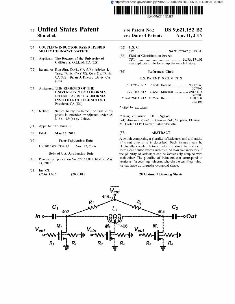
FIG. 4 illustrates a coupling inductor based hybrid mm-wave switch in accordance with some embodimentsdescribed herein. In FIG. 4, resistors R1 through R6 can be10 kQ, resistors R, and R$ can be 14 kQ, capacitances C1
and C2 can be 300 IF, inductance L1 can be 102 pH, andtransistors M, through M3 can have dimensions 4 µmx60nmx15. Port "In" can be the input port, port "Out" can be theoutput port, and voltage V,,,, can be the control voltage thatis used to toggle the switch operating mode. Capacitances C1
and C2 are DC-block capacitors. The resistance, capacitance,inductance, and transistor parameters described above havebeen selected for the switch to operate in the E-band. It willbe apparent to a person having ordinary skill in the art thata different set of parameter values may be selected if theswitch is desired to be operated in a different frequencyband.Some embodiments of a switch can comprise one or more
inductors (each inductor can be a lumped inductor) and aplurality of shunt transistors. Specifically, a switch cancomprise a first inductor having a first terminal and a secondterminal, a second inductor having a first terminal and asecond terminal, wherein the second terminal of the firstinductor is electrically connected with the first terminal ofthe second inductor, and wherein a negative mutual induc-tance exists between the first inductor and the secondinductor. In some embodiments, the first inductor can be aportion of a coupling inductor that begins at a first terminalof the coupling inductor and ends at a tap of the couplinginductor, and the second inductor can be a portion of thecoupling inductor that begins at the tap of the couplinginductor and ends at a second terminal of the couplinginductor.The plurality of shunt transistors can comprise (1) a first
shunt transistor controlled by a control voltage, wherein thefirst shunt transistor is electrically connected between thefirst terminal of the first inductor and a first shunt terminalhaving a shunt voltage (e.g., the shunt voltage can beground, but generally the shunt voltage can be any voltageto which the input signal is shunted when the switch is in the"open" state); (2) a second shunt transistor controlled by thecontrol voltage, wherein the second shunt transistor is elec-trically connected between the second terminal of the firstinductor and a second shunt terminal having the shuntvoltage; and (3) a third shunt transistor controlled by thecontrol voltage, wherein the third shunt transistor is electri-cally connected between the second terminal of the secondinductor and a third shunt terminal having the shunt voltage.The embodiment shown in FIG. 4 comprises (1) a cou-
pling inductor L1 having a first terminal 402, a second
10terminal 404, and a tap 406, (2) a first shunt transistor M,controlled by a control voltage V,,,,,, wherein the first shunttransistor M1 is electrically connected between the firstterminal 402 of the coupling inductor L, and a terminal
5 having a shunt voltage (e.g., in FIG. 4, the shunt voltage isshown to be ground, but generally the shunt voltage can beany voltage to which the input signal is to be shunted whenthe switch is in the "open" state), (3) a second shunttransistor Mz controlled by the control voltage V,,,,,, wherein
to the second shunt transistor Mz is electrically connectedbetween the tap 406 of the coupling inductor L, and aterminal having the shunt voltage; and (4) a third shunttransistor M3 controlled by the control voltage V,,,,,, wherein
15 the third shunt transistor M3 is electrically connectedbetween the second terminal 404 of the coupling inductor L,and a terminal having the shunt voltage.As explained above, a negative mutual inductance can
exist between (1) a first portion of the coupling inductor L,20 that begins at the first terminal 402 of the coupling inductor
L, and ends at the tap 406 of the coupling inductor L1, and(2) a second portion of the coupling inductor L1 that beginsat the tap 406 of the coupling inductor L1 and ends at thesecond terminal 404 of the coupling inductor L1.
25 As shown in FIG. 4, the switch can further comprise: (1)an input port "In" to receive an input signal; (2) an outputport "Out" to output an output signal; (3) a first capacitor C1
electrically connected between the input port "In" and thefirst terminal 402 of the coupling inductor Ll; and (4) a
30 second capacitor C2 electrically connected between theoutput port "Out" and the second terminal 404 of thecoupling inductor L1.In some embodiments, the switch can further comprise:
(1) a first resistor R, electrically connected between the first35 terminal 402 of the coupling inductor L1 and a reverse
polarity terminal 408 having a reversed polarity of thecontrol voltage V,,,; and (2) a second resistor R$ electricallyconnected between the second terminal 404 of the couplinginductor L1 and the reverse polarity terminal 408 having the
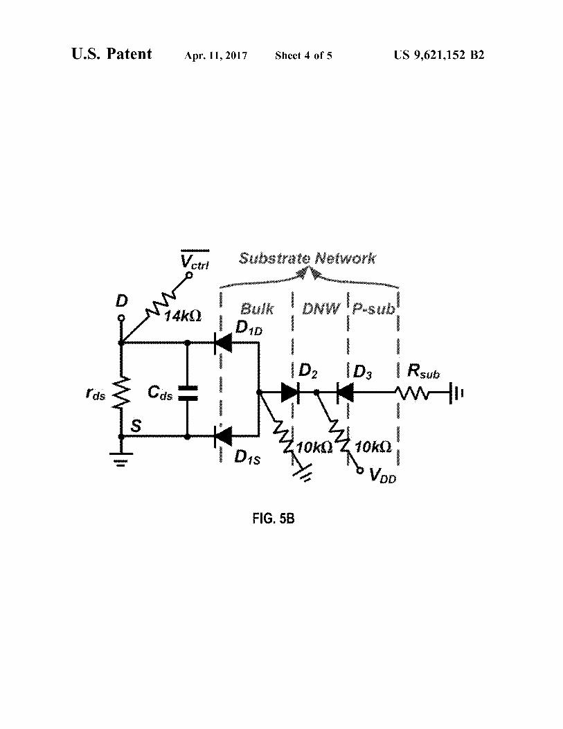
4o reversed polarity of the control voltage V,,,.FIG. 5A illustrates a cross-sectional view of a triple-well
MOSFET in accordance with some embodiments describedherein. FIG. 5B illustrates an equivalent circuit correspond-ing to the MOSFET shown in FIG. 5A in accordance with
45 some embodiments described herein.The triple-well MOSFET shown in FIG. 5A can be
fabricated using triple-well CMOS technology, which offersa better performance in terms of isolation and bulk voltagecontrol. Note that the substrate network has three embedded
5o reverse-biased diodes. In this design, two specific biases areapplied to the switch transistor as depicted in FIG. 5B. Firstis the drain bias. The transistor's drain is biased to thereversed polarity of the control voltage. This configuration isdifferent with the regular mm-wave switch design, which
55 usually leaves the drain unbiased. The other one provides thebody bias control. The P-well bulk is biased to ground andthe deep-Nwell (DNW) is biased to a supply voltage, boththrough 10 kQ large resistors.As shown in FIG. 513, the bias on the bulk and DNW
6o allow the diodes D1D_s, D2 and D3 to be reversely biased,even if the transistor is operating in large-signal mode. Thisincreases the equivalent impedance of the whole substratenetwork at the drain. The 10 kQ bias resistors help to isolatethe alternating current (AC) signals, which helps improve
65 the power handling capability of the switch. Moreover, areverse-biased diode behaves as a voltage-controlled capaci-tor. The capacitance can be expressed as:

11
Ci
Co_
Vbt —
US 9,621,152 B2
where Co is the capacitance with zero reverse bias, Vb isthe reversed bias voltage and ~ is the contact potential of thepn junction. Therefore, applied body bias also reduces para-sitic capacitance of the substrate network.
Another special bias scheme is to bias the transistor'sdrain to the reversed polarity of the control voltage, asshown in FIG. 5B. When the transistor turns off, the drain isbiased at VDD. The equivalent output impedance of theturn-off transistor is defined as:
a VDSrd, _
_a IDS
In weak inversion region, the expression of the draincurrent is
as
I l ex VcS — Vth
1 — ex _ VDSD = o p~
nVT ~~ p~ VT ~~
When VGS equals to zero, the expression of r,, is derived
VT VDS Vthrd, _ T exp(
V + nVo T t
The r,, increases dramatically with a large Vds. Theincrease of r,, results in an improvement of equivalentimpedance R... Equivalent Co-g- and R o-g for different tran-sistor size under different bias schemes were extracted. Theresults showed that C f does not change much. However,
Roff experienced a significant increase with the bulk floatingand drain bias. For instance, the equivalent R f of the 60 µmtransistor increases from 290Q to 960Q by applying bulkfloating, and then increases further to 1.5 kQ with thereverse drain bias technique together. These improvementsultimately lead to lower insertion loss. Approximate 0.5 dBimprovement was observed in the simulation by applyingthis bias scheme.The influence of the coupling effect on insertion loss and
isolation is now analyzed. The coupling coefficient is usedhere for the optimization to give a normalized view point,which is defined as:
M Mk= _
Lz
The inductors are modelled with a first order 71 model witha series resistor and the parasitic parallel capacitors. Thedesign target is to achieve isolation higher than 35 dB withacceptable insertion loss in the E-band. However, due toparasitic capacitance, the increased inductance only benefitsthe isolation in the low frequency band. The coupling effectdegrades the isolation in the high frequency range. Consid-ering a compromise between isolation and insertion loss, thepreferred k was found to be around —0.26.
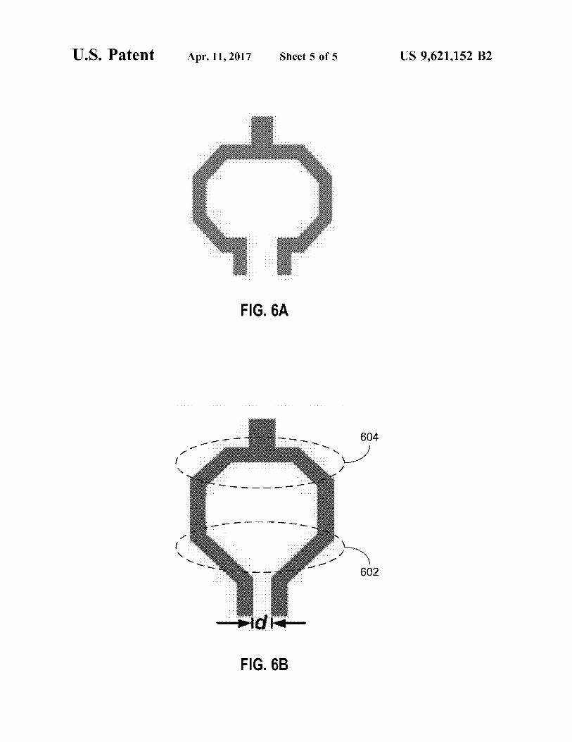
12It is important to appropriately design the coupling induc-
tor. In the E-band, it is not difficult to realize an inductor withquality factor higher than 20. So, the concern during induc-tor design is not the quality factor, but the inductance and the
5 coupling coefficient. FIG. 6A illustrates a regular octagonshaped inductor in accordance with some embodimentsdescribed herein. In some embodiments, in order to vary thecoupling coefficient and inductance, the coupled inductordesign does not use a regular octagon shape as shown in
io FIG. 6A. FIG. 6B illustrates an irregular octagon shapedinductor design in accordance with some embodimentsdescribed herein. Instead of using the regular octagon shapeshown in FIG. 6A, some embodiments described herein usean inductor in which the lower part 602 has a different size
15 from the upper part 604, meanwhile the distance "d"between the two terminals can be adjusted, as shown in FIG.6B. These changes of inductor's shape both affect thecoupling coefficient and inductance value. The ultimateinductor optimization is verified by electromagnetic simu-
20 lation. In one embodiment, the designed inductor results in102 pH inductance with approximately a —0.28 couplingcoefficient.One implementation of the switch was fabricated using a
standard bulk 65 nm CMOS technology with a 6-metal25 back-end. The switch core circuit occupied only 100x120
µm2 area. The resulting switch had the following parameters(which are better than other existing approaches): (1) oper-ating bandwidth was 54-84 GHz, (2) minimum insertion losswas 1.7 dB, (3) return loss was less than 10 dB, (4) isolation
30 was greater than 35 dB, (5) input-referred PI dB compres-sion-point in the pass-mode was 10.5 dBm, (6) core area was0.012 mm2, and (7) the switch was fabricated in a 65 mmCMOS process.The foregoing description has been presented to enable
35 any person skilled in the art to make and use the embodi-ments. The described embodiments are not intended to beexhaustive or to limit the present invention. Various modi-fications to the disclosed embodiments will be readily appar-ent to those skilled in the art, and the general principles
4o defined herein are applicable to other embodiments andapplications without departing from the spirit and scope ofthe present disclosure. Thus, the present invention is to beaccorded the widest scope consistent with the principles andfeatures disclosed herein. The scope of the present invention
45 is defined by the appended claims.
What is claimed is:1. A switch, comprising:a plurality of inductors, comprising a first inductor having
50 a first terminal and a second terminal, a second inductorhaving a first terminal and a second terminal, whereinthe second terminal of the first inductor is electricallyconnected with the first terminal of the second inductor,and wherein a negative mutual inductance exists
55 between the first inductor and the second inductor; anda plurality of shunt transistors, comprising:
a first shunt transistor controlled by a control voltage,wherein the first shunt transistor is electrically con-nected between the first terminal of the first inductor
60 and a first shunt terminal having a shunt voltage;a second shunt transistor controlled by the control
voltage, wherein the second shunt transistor is elec-trically connected between the second terminal of thefirst inductor and a second shunt terminal having the
65 shunt voltage; anda third shunt transistor controlled by the control volt-
age, wherein the third shunt transistor is electrically

US 9,621,152 B2
13connected between the second terminal of the secondinductor and a third shunt terminal having the shuntvoltage.
2. The switch of claim 1, wherein the shunt voltage isground.
3. The switch of claim 1, wherein the first inductor is aportion of a coupling inductor that begins at a first terminalof the coupling inductor and ends at a tap of the couplinginductor, and wherein the second inductor is a portion of thecoupling inductor that begins at the tap of the couplinginductor and ends at a second terminal of the couplinginductor.
4. The switch of claim 3, wherein the coupling inductorhas an irregular octagonal shape.
5. The switch of claim 1, further comprising:an input port to receive an input signal;an output port to output an output signal;a first capacitor electrically connected between the input
port and the first terminal of the first inductor; anda second capacitor electrically connected between the
output port and the second terminal of the secondinductor.
6. The switch of claim 1, further comprising:a first resistor electrically connected between the first
terminal of the first inductor and a reverse polarityterminal having a reversed polarity of the controlvoltage; and
a second resistor electrically connected between the sec-ond terminal of the second inductor and the reversepolarity terminal having the reversed polarity of thecontrol voltage.
7. The switch of claim 1, wherein each shunt transistor hasa triple-well structure comprising a P-well bulk, a deep-Nwell, and a P-substrate, wherein the P-well bulk is biasedto ground, and the deep-Nwell is biased to a supply voltage.
8. A device, comprising:a first circuit to generate a millimeter (mm)-wave signal;a second circuit to receive the mm-wave signal; anda switch electrically connected between the first circuit
and the second circuit, the switch comprising:a plurality of inductors, comprising a first inductor
having a first terminal and a second terminal, asecond inductor having a first terminal and a secondterminal, wherein the second terminal of the firstinductor is electrically connected with the first ter-minal of the second inductor, and wherein a negativemutual inductance exists between the first inductorand the second inductor; and
a plurality of shunt transistors, comprising:a first shunt transistor controlled by a control volt-
age, wherein the first shunt transistor is electri-cally connected between the first terminal of thefirst inductor and a first shunt terminal having ashunt voltage;
a second shunt transistor controlled by the controlvoltage, wherein the second shunt transistor iselectrically connected between the second termi-nal of the first inductor and a second shunt termi-nal having the shunt voltage; and
a third shunt transistor controlled by the controlvoltage, wherein the third shunt transistor is elec-trically connected between the second terminal ofthe second inductor and a third shunt terminalhaving the shunt voltage.
9. The device of claim 8, wherein the shunt voltage isground.
1410. The device of claim 8, wherein the first inductor is a
portion of a coupling inductor that begins at a first terminalof the coupling inductor and ends at a tap of the couplinginductor, and wherein the second inductor is a portion of the
5 coupling inductor that begins at the tap of the couplinginductor and ends at a second terminal of the couplinginductor.
11. The device of claim 10, wherein the coupling inductorhas an irregular octagonal shape.
10 12. The device of claim 8, wherein the switch furthercomprises:an input port to receive the mm-wave signal;an output port to output the mm-wave signal;a first capacitor electrically connected between the input
15 port and the first terminal of the first inductor; anda second capacitor electrically connected between the
output port and the second terminal of the secondinductor.
13. The device of claim 8, wherein the switch further20 comprises:
a first resistor electrically connected between the firstterminal of the first inductor and a reverse polarityterminal having a reversed polarity of the controlvoltage; and
25 a second resistor electrically connected between the sec-ond terminal of the second inductor and the reversepolarity terminal having the reversed polarity of thecontrol voltage.
14. The device of claim 8, wherein each shunt transistorso has a triple-well structure comprising a P-well bulk, a
deep-Nwell, and a P-substrate, wherein the P-well bulk isbiased to ground, and the deep-Nwell is biased to a supplyvoltage.15. A circuit, comprising:
35 a plurality of switches, wherein each switch comprises:a coupling inductor having a first terminal, a second
terminal, and a tap;a first shunt transistor controlled by a control voltage,
wherein the first shunt transistor is electrically con-40 nected between the first terminal of the coupling
inductor and a first shunt terminal having a shuntvoltage;
a second shunt transistor controlled by the controlvoltage, wherein the second shunt transistor is elec-
45 trically connected between the tap of the couplinginductor and a second shunt terminal having theshunt voltage; and
a third shunt transistor controlled by the control volt-age, wherein the third shunt transistor is electrically
50 connected between the second terminal of the cou-pling inductor and a third shunt terminal having theshunt voltage.
16. The circuit of claim 15, wherein the shunt voltage isground.
55 17. The circuit of claim 15, wherein a negative mutualinductance exists between (1) a first portion of the couplinginductor that begins at the first terminal of the couplinginductor and ends at the tap of the coupling inductor, and (2)a second portion of the coupling inductor that begins at the
60 tap of the coupling inductor and ends at the second terminalof the coupling inductor.18. The circuit of claim 15, wherein each switch further
comprises:a first resistor electrically connected between the first
65 terminal of the coupling inductor and a reverse polarityterminal having a reversed polarity of the controlvoltage; and

US 9,621,152 B2
15 16a second resistor electrically connected between the sec-ond terminal of the coupling inductor and the reversepolarity terminal having the reversed polarity of thecontrol voltage.
19. The circuit of claim 15, wherein each shunt transistor 5
has a triple-well structure comprising a P-well bulk, adeep-Nwell, and a P-substrate, wherein the P-well bulk isbiased to ground, and the deep-Nwell is biased to a supplyvoltage.
20. The circuit of claim 15, wherein the coupling inductor iohas an irregular octagonal shape.