1,2 3 3,4,5, 7 - physics main | physics
TRANSCRIPT

crystals
Article
Deep Etched Gallium Nitride Waveguide for RamanSpectroscopic Applications
Yu-Li Hsieh 1,2, Wen-Shao Chen 3, Liann-Be Chang 3,4,5,* , Lee Chow 6 , Samuel Borges, Jr. 7,Alfons Schulte 8 , Shiang-Fu Huang 5 , Ming-Jer Jeng 1,5,* and Chih-Jen Yu 3,5
1 Department of Electronics Engineering, Chang Gung University, Guishan, Taoyuan 333, Taiwan;[email protected]
2 Department of Electrical and Electronic Engineering, Chung Cheng Institute of Technology,National Defense University, Daxi, Taoyuan 335, Taiwan
3 Green Technology Research Center, Chang Gung University, Guishan, Taoyuan 333, Taiwan;[email protected] (W.-S.C.); [email protected] (C.-J.Y.)
4 Department of Materials Engineering, Ming Chi University of Technology, Taishan,New Taipei City 243, Taiwan
5 Department of Otolaryngology-Head and Neck Surgery, Chang Gung Memorial Hospital, Linkou,Taoyuan 333, Taiwan; [email protected]
6 Department of Physics and NanoScience Technology Center, University of Central Florida, Orlando,FL 32816, USA; [email protected]
7 Department of Physics, University of Central Florida, Orlando, FL 32816, USA; [email protected] Department of Physics and College of Optics and Photonics, University of Central Florida, Orlando,
FL 32816, USA; [email protected]* Correspondence: [email protected] (L.-B.C.); [email protected] (M.-J.J.);
Tel.: +886-3-211-8800 (ext. 5793) (L.-B.C.); +886-3-211-8800 (ext. 3507) (M.-J.J.);Fax: +886-3-211-8507 (L.-B.C. & M.-J.J.)
Received: 29 January 2019; Accepted: 23 March 2019; Published: 26 March 2019�����������������
Abstract: Gallium nitride (GaN) materials with a high chemical stability and biocompatibility arewell suited for bio-sensing applications and evanescent wave spectroscopy. However, GaN poseschallenges for processing, especially for deep etching using conventional etching techniques. Here,we present a dry-etching technique using tetraethyl orthosilicate (TEOS) oxide as an etching barrier.We demonstrate that a sharp, vertically-etched waveguide pattern can be obtained with low surfaceroughness. The fabricated GaN waveguide structure is further characterized using field-emissionscanning electron microscopy, Raman spectroscopy, and a stylus profilometer.
Keywords: Gallium nitride (GaN); waveguide; semiconductor processing; tetraethylorthosilicate (TEOS)
1. Introduction
Gallium Nitride (GaN) is a III-V group compound semiconductor. It can exist in either wurtziteform or zinc-blende form. The wurtzite modification of GaN is slightly more common and has a widedirect band gap of 3.4 eV at room temperature [1]. The direct band gap enables the use of GaN forhighly efficient light emitting diodes (LEDs) [2], laser diodes (LDs), and UV detectors. In the last fifteenyears, the efficiency of GaN-based LEDs has improved greatly, making solid state lighting available [3].GaN offers several other attractive properties, including a high breakdown field, EB = 4.0 MV/cm,a high electron mobility, µ = 1300 cm2
V·s , and a large dielectric constant of ε = 9.0. These parameterscombined with the large band gap make GaN an excellent candidate for high power RF devices [4,5].Gallium Nitride (GaN) is also well suited for bio-sensor applications due to its chemical stability,
Crystals 2019, 9, 176; doi:10.3390/cryst9030176 www.mdpi.com/journal/crystals

Crystals 2019, 9, 176 2 of 8
wide spectral transmission window, and biocompatibility [6]. Although dry etching using inductivelycoupled plasma (ICP) has been employed in the past [7], deep etching of up to 5 µm of thick GaN filmsis rare. More recently GaN has attracted increased interest for integrated photonic applications [8,9].
For waveguide application employing evanescent excitation, a low surface roughness of thewaveguide and a sharp etching profile are essential. For optical coupling from the end-face of theGaN waveguide, the cross-section of the waveguide needs to be in the range of microns. Therefore,deep etching a thick GaN film to create a waveguide structure is of significant interest.
Using a conventional photoresist as an etching barrier does not provide enough depth for a GaNwaveguide. If the photoresist is not sufficiently thick in spin coating, it will not effectively block theion bombardment during the inductively coupled plasma (ICP) etching. This causes over-etching ofthe waveguide, reducing not only the height of the waveguide, but also creating a rough surface as aresult of ion bombardment. On the other hand, if an excessively thick coating of photoresist is formed,the exposure and development process will be non-uniform, leading to the poor development of thephotoresist and preventing the fabrication of the waveguide. A denser and more uniform material isrequired as an etch barrier to improve the etching process. Tetraethyl Orthosilicate (TEOS), due to itsexcellent step coverage, is the reactive gas widely used in chemical vapor deposition to deposit a denseand uniform silicon oxide film. TEOS has a favorable surface mobility and gap-filling ability [10–12].Therefore, TEOS deposited oxide is used and studied as the etching barrier for deep etching in thepresent work. Various widths of GaN waveguides were experimentally fabricated.
2. Experimental Section
Initially, a 2-inch mask was constructed with waveguide patterns at various widths, as shown inFigure 1a. After that, commercial 2-inch sapphire substrates with a 5 µm GaN thin film epitaxiallygrown by MOCVD were cleaned with a standard RCA procedure in an ultrasonic bath with acetone,isopropanol and de-ionized water for 3 minutes each sequentially. Subsequently, 2 µm of TetraethylOrthosilicate (TEOS) oxide was deposited to form the SiO2 layer on top of the wafers as the first etchingbarrier by plasma enhanced chemical vapor deposition (PECVD). Next, a PR-5214 photoresist with athickness of 1.5 µm was spin-coated on the substrate wafers. An exposure system was used to developthe desired waveguide patterns (2, 4 and 8 µm, respectively), as shown in Figure 1b.
Crystals 2019, 9, x FOR PEER REVIEW 2 of 8
power RF devices [4,5]. Gallium Nitride (GaN) is also well suited for bio-sensor applications due to its chemical stability, wide spectral transmission window, and biocompatibility [6]. Although dry etching using inductively coupled plasma (ICP) has been employed in the past [7], deep etching of up to 5μm of thick GaN films is rare. More recently GaN has attracted increased interest for integrated photonic applications [8,9].
For waveguide application employing evanescent excitation, a low surface roughness of the waveguide and a sharp etching profile are essential. For optical coupling from the end-face of the GaN waveguide, the cross-section of the waveguide needs to be in the range of microns. Therefore, deep etching a thick GaN film to create a waveguide structure is of significant interest.
Using a conventional photoresist as an etching barrier does not provide enough depth for a GaN waveguide. If the photoresist is not sufficiently thick in spin coating, it will not effectively block the ion bombardment during the inductively coupled plasma (ICP) etching. This causes over-etching of the waveguide, reducing not only the height of the waveguide, but also creating a rough surface as a result of ion bombardment. On the other hand, if an excessively thick coating of photoresist is formed, the exposure and development process will be non-uniform, leading to the poor development of the photoresist and preventing the fabrication of the waveguide. A denser and more uniform material is required as an etch barrier to improve the etching process. Tetraethyl Orthosilicate (TEOS), due to its excellent step coverage, is the reactive gas widely used in chemical vapor deposition to deposit a dense and uniform silicon oxide film. TEOS has a favorable surface mobility and gap-filling ability [10–12]. Therefore, TEOS deposited oxide is used and studied as the etching barrier for deep etching in the present work. Various widths of GaN waveguides were experimentally fabricated.
2. Experimental Section
Initially, a 2-inch mask was constructed with waveguide patterns at various widths, as shown in Figure 1a. After that, commercial 2-inch sapphire substrates with a 5μm GaN thin film epitaxially grown by MOCVD were cleaned with a standard RCA procedure in an ultrasonic bath with acetone, isopropanol and de-ionized water for 3 minutes each sequentially. Subsequently, 2 μm of Tetraethyl Orthosilicate (TEOS) oxide was deposited to form the SiO2 layer on top of the wafers as the first etching barrier by plasma enhanced chemical vapor deposition (PECVD). Next, a PR-5214 photoresist with a thickness of 1.5 μm was spin-coated on the substrate wafers. An exposure system was used to develop the desired waveguide patterns (2, 4 and 8 μm, respectively), as shown in Figure 1b.
(a)
(b)
Figure 1. (a) Waveguide patterns on a 2-inch mask; and (b) Waveguide pattern images of 2, 4 and 8 μm after exposure developed.
After the deposition of the etching barriers, wafers were etched using an inductively coupled plasma reactive ion etching system. This created a deep-etched GaN waveguide structure. All of the etching parameters of the system such as the ICP source power, RF bias power, chamber pressure
Figure 1. (a) Waveguide patterns on a 2-inch mask; and (b) Waveguide pattern images of 2, 4 and 8 µmafter exposure developed.
After the deposition of the etching barriers, wafers were etched using an inductively coupledplasma reactive ion etching system. This created a deep-etched GaN waveguide structure. All of theetching parameters of the system such as the ICP source power, RF bias power, chamber pressureand gas flows were optimized in the experiment. The fabricated GaN waveguide structure wascharacterized by a stylus profilometer (Alpha-Stepper; Surfcorder ET3000, Kosaka Laboratory Ltd.,Tokyo, Japan), a field emission scanning electron microscope (SEM; SU8220, Hitachi High-Technologies,

Crystals 2019, 9, 176 3 of 8
Tokyo, Japan and JSM-7500F, JEOL, Tokyo, Japan), an energy dispersive X-ray spectrometer (EDS;INCA X-ACT, OXFORD, High Wycombe, UK), and an atomic force microscope (AFM; NT-MDT SolverP47, NT-MDT Spectrum Instruments, Moscow, Russia).
3. Results and Discussion
Inductively coupled plasma reactive ion etching (ICP-RIE etching) to create an anisotropic GaNetching depth up to 5 µm is not well understood [13,14]. The choices of the etching-resistant material,etching gas, and etching time are crucial to ensure the success of the etching process. If the etchingtime is too long, then the waveguide will be partially etched. This results in an uneven waveguidesurface and scattering of the laser signal due to surface roughness in the waveguide. If the etchingtime is too short, the isolated waveguide cannot form, which will cause some loss of signal [15].
The top of the sapphire substrate was covered with a 5 µm thick GaN epilayer. Initially, only onesingle photoresist (PR) layer was used as an etching barrier. To shape the perfect waveguide withetching to the sapphire substrate, a long etching time (1500 s) was used. However, after the etchingprocess, the etching resistance of the PR mask was neither as expected nor sufficient to provide adeep etch of 5 µm in the GaN. The resulting waveguide displayed a damaged surface and damagedside walls, as shown in Figure 2. This is clearly unacceptable for use as a waveguide. In addition,the waveguides were characterized with a profilometer. The surface profiles are shown in Figure 3.The height of the waveguide is not uniform, and the non-uniform exposure has almost destroyed the 2µm wide waveguide.
Crystals 2019, 9, x FOR PEER REVIEW 3 of 8
and gas flows were optimized in the experiment. The fabricated GaN waveguide structure was characterized by a stylus profilometer (Alpha-Stepper; Surfcorder ET3000, Kosaka Laboratory Ltd., Tokyo, Japan), a field emission scanning electron microscope (SEM; SU8220, Hitachi High-Technologies, Tokyo, Japan and JSM-7500F, JEOL, Tokyo, Japan), an energy dispersive X-ray spectrometer (EDS; INCA X-ACT, OXFORD, High Wycombe, UK), and an atomic force microscope (AFM; NT-MDT Solver P47, NT-MDT Spectrum Instruments, Moscow, Russia).
3. Results and Discussion
Inductively coupled plasma reactive ion etching (ICP-RIE etching) to create an anisotropic GaN etching depth up to 5 μm is not well understood [13,14]. The choices of the etching-resistant material, etching gas, and etching time are crucial to ensure the success of the etching process. If the etching time is too long, then the waveguide will be partially etched. This results in an uneven waveguide surface and scattering of the laser signal due to surface roughness in the waveguide. If the etching time is too short, the isolated waveguide cannot form, which will cause some loss of signal [15].
The top of the sapphire substrate was covered with a 5 μm thick GaN epilayer. Initially, only one single photoresist (PR) layer was used as an etching barrier. To shape the perfect waveguide with etching to the sapphire substrate, a long etching time (1500 s) was used. However, after the etching process, the etching resistance of the PR mask was neither as expected nor sufficient to provide a deep etch of 5 μm in the GaN. The resulting waveguide displayed a damaged surface and damaged side walls, as shown in Figure 2. This is clearly unacceptable for use as a waveguide. In addition, the waveguides were characterized with a profilometer. The surface profiles are shown in Figure 3. The height of the waveguide is not uniform, and the non-uniform exposure has almost destroyed the 2 μm wide waveguide.
Figure 2. SEM images of a GaN waveguide with a damaged surface and side walls.
Figure 3. Surface profile of the GaN waveguide fabricated with one single photoresist (PR) layer as an etching barrier.
Figure 2. SEM images of a GaN waveguide with a damaged surface and side walls.
Crystals 2019, 9, x FOR PEER REVIEW 3 of 8
and gas flows were optimized in the experiment. The fabricated GaN waveguide structure was characterized by a stylus profilometer (Alpha-Stepper; Surfcorder ET3000, Kosaka Laboratory Ltd., Tokyo, Japan), a field emission scanning electron microscope (SEM; SU8220, Hitachi High-Technologies, Tokyo, Japan and JSM-7500F, JEOL, Tokyo, Japan), an energy dispersive X-ray spectrometer (EDS; INCA X-ACT, OXFORD, High Wycombe, UK), and an atomic force microscope (AFM; NT-MDT Solver P47, NT-MDT Spectrum Instruments, Moscow, Russia).
3. Results and Discussion
Inductively coupled plasma reactive ion etching (ICP-RIE etching) to create an anisotropic GaN etching depth up to 5 μm is not well understood [13,14]. The choices of the etching-resistant material, etching gas, and etching time are crucial to ensure the success of the etching process. If the etching time is too long, then the waveguide will be partially etched. This results in an uneven waveguide surface and scattering of the laser signal due to surface roughness in the waveguide. If the etching time is too short, the isolated waveguide cannot form, which will cause some loss of signal [15].
The top of the sapphire substrate was covered with a 5 μm thick GaN epilayer. Initially, only one single photoresist (PR) layer was used as an etching barrier. To shape the perfect waveguide with etching to the sapphire substrate, a long etching time (1500 s) was used. However, after the etching process, the etching resistance of the PR mask was neither as expected nor sufficient to provide a deep etch of 5 μm in the GaN. The resulting waveguide displayed a damaged surface and damaged side walls, as shown in Figure 2. This is clearly unacceptable for use as a waveguide. In addition, the waveguides were characterized with a profilometer. The surface profiles are shown in Figure 3. The height of the waveguide is not uniform, and the non-uniform exposure has almost destroyed the 2 μm wide waveguide.
Figure 2. SEM images of a GaN waveguide with a damaged surface and side walls.
Figure 3. Surface profile of the GaN waveguide fabricated with one single photoresist (PR) layer as an etching barrier. Figure 3. Surface profile of the GaN waveguide fabricated with one single photoresist (PR) layer as anetching barrier.
In order to improve the etching process, an extra oxide layer of TEOS, which acted as a precursorfor the deposition of SiO2, was deposited on top of the GaN layer by PECVD before the photoresist

Crystals 2019, 9, 176 4 of 8
coating. After the development of the photoresist coating, Ar and CF4 gases were used as etchantsto remove the photoresist barrier layer while the SiO2 layer acted as an etch barrier to protect theGaN. Since the SiO2 layer is relatively stable in the etching process, it blocks etching gases suchas Cl2 and BCl3. Figure 4 shows the etching process. To improve the deep etching and to reducethe complexity of the process, the relevant parameters were optimized. In the initial stage of theexperiment, a selectivity ratio of 1:1 of the photoresist to GaN was chosen. However, a spin-coatingphotoresist with a thickness of 5 µm is difficult to form in the lithography process. SiO2 was addedto the photoresist layer in the manufacturing process. SiO2, deposited by PECVD as an ICP etchingbarrier, is commonly used in semiconductor processing and exhibits an excellent deposition uniformityat high selectivity ratios. Therefore, Ar and CF4 gases were first used to etch out the layer pattern ofthe SiO2 barrier. Subsequently, Cl2 and BCl3 gases were used to etch the GaN layer with the etchingparameters listed in Table 1.
Crystals 2019, 9, x FOR PEER REVIEW 4 of 8
In order to improve the etching process, an extra oxide layer of TEOS, which acted as a precursor for the deposition of SiO2, was deposited on top of the GaN layer by PECVD before the photoresist coating. After the development of the photoresist coating, Ar and CF4 gases were used as etchants to remove the photoresist barrier layer while the SiO2 layer acted as an etch barrier to protect the GaN. Since the SiO2 layer is relatively stable in the etching process, it blocks etching gases such as Cl2 and BCl3. Figure 4 shows the etching process. To improve the deep etching and to reduce the complexity of the process, the relevant parameters were optimized. In the initial stage of the experiment, a selectivity ratio of 1:1 of the photoresist to GaN was chosen. However, a spin-coating photoresist with a thickness of 5 μm is difficult to form in the lithography process. SiO2 was added to the photoresist layer in the manufacturing process. SiO2, deposited by PECVD as an ICP etching barrier, is commonly used in semiconductor processing and exhibits an excellent deposition uniformity at high selectivity ratios. Therefore, Ar and CF4 gases were first used to etch out the layer pattern of the SiO2 barrier. Subsequently, Cl2 and BCl3 gases were used to etch the GaN layer with the etching parameters listed in Table 1.
Table 1. The ICP etching parameters.
Etching Step
Target Material
Source Power
Bias Power Pressure Using Gas 1
Using Gas 2
1 SiO2 1000 W 200 W 1 Pa Ar 40sccm CF4 70 sccm 2 GaN 500 W 300 W 1 Pa Cl2 60sccm BCl3 60 sccm
Figure 4. Process for the fabrication of a deep etched GaN waveguide.
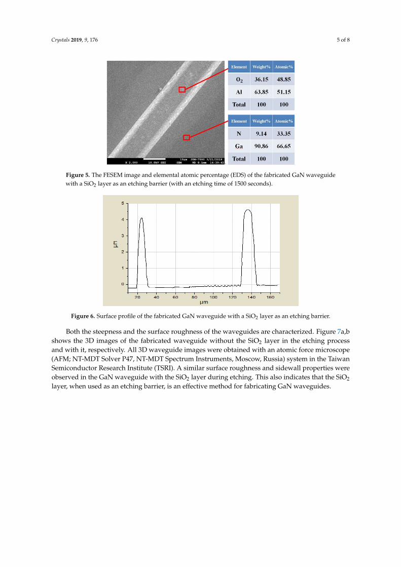
Figure 5 displays a FESEM image and elemental atomic percentage of a GaN waveguide coated with an SiO2 layer as an etching barrier. The etching time was 1500 seconds. A comparison of Figures 2 and 5 demonstrates that an extra oxide layer, SiO2, greatly reduced the roughness of the GaN waveguide surface (for a fixed etching time of 1500 s), and enabled a 5 μm-deep GaN etching of the sapphire substrate. Etching parameter combinations should be analyzed in the future to optimize results. The scanning electron microscopy (SEM; JSM-7500F, JEOL, Tokyo, Japan) image and elemental composition (energy dispersive spectroscopy, EDS; INCA X-ACT, OXFORD, High Wycombe, UK) in Figure 5 indicate the success of the above process with proper etch selectivity ratios to produce the desired GaN waveguide. Figure 6 displays the results of a 5 μm-deep etching. Through this process, a useful GaN waveguide was fabricated.
Figure 4. Process for the fabrication of a deep etched GaN waveguide.
Table 1. The ICP etching parameters.
EtchingStep
TargetMaterial
SourcePower
BiasPower Pressure Using
Gas 1UsingGas 2
1 SiO2 1000 W 200 W 1 Pa Ar 40 sccm 70 sccm2 GaN 500 W 300 W 1 Pa Cl2 60 sccm BCl3 60 sccm
Figure 5 displays a FESEM image and elemental atomic percentage of a GaN waveguide coatedwith an SiO2 layer as an etching barrier. The etching time was 1500 seconds. A comparison ofFigures 2 and 5 demonstrates that an extra oxide layer, SiO2, greatly reduced the roughness of theGaN waveguide surface (for a fixed etching time of 1500 s), and enabled a 5 µm-deep GaN etching ofthe sapphire substrate. Etching parameter combinations should be analyzed in the future to optimizeresults. The scanning electron microscopy (SEM; JSM-7500F, JEOL, Tokyo, Japan) image and elementalcomposition (energy dispersive spectroscopy, EDS; INCA X-ACT, OXFORD, High Wycombe, UK) inFigure 5 indicate the success of the above process with proper etch selectivity ratios to produce thedesired GaN waveguide. Figure 6 displays the results of a 5 µm-deep etching. Through this process,a useful GaN waveguide was fabricated.
Crystals 2019, 9, 176 5 of 8
Crystals 2019, 9, x FOR PEER REVIEW 5 of 8
Figure 5. The FESEM image and elemental atomic percentage (EDS) of the fabricated GaN waveguide with a SiO2 layer as an etching barrier (with an etching time of 1500 seconds).
Figure 6. Surface profile of the fabricated GaN waveguide with a SiO2 layer as an etching barrier.
Both the steepness and the surface roughness of the waveguides are characterized. Figure 7a,b shows the 3D images of the fabricated waveguide without the SiO2 layer in the etching process and with it, respectively. All 3D waveguide images were obtained with an atomic force microscope (AFM; NT-MDT Solver P47, NT-MDT Spectrum Instruments, Moscow, Russia) system in the Taiwan Semiconductor Research Institute (TSRI). A similar surface roughness and sidewall properties were observed in the GaN waveguide with the SiO2 layer during etching. This also indicates that the SiO2 layer, when used as an etching barrier, is an effective method for fabricating GaN waveguides.
Figure 5. The FESEM image and elemental atomic percentage (EDS) of the fabricated GaN waveguidewith a SiO2 layer as an etching barrier (with an etching time of 1500 seconds).
Crystals 2019, 9, x FOR PEER REVIEW 5 of 8
Figure 5. The FESEM image and elemental atomic percentage (EDS) of the fabricated GaN waveguide with a SiO2 layer as an etching barrier (with an etching time of 1500 seconds).
Figure 6. Surface profile of the fabricated GaN waveguide with a SiO2 layer as an etching barrier.
Both the steepness and the surface roughness of the waveguides are characterized. Figure 7a,b shows the 3D images of the fabricated waveguide without the SiO2 layer in the etching process and with it, respectively. All 3D waveguide images were obtained with an atomic force microscope (AFM; NT-MDT Solver P47, NT-MDT Spectrum Instruments, Moscow, Russia) system in the Taiwan Semiconductor Research Institute (TSRI). A similar surface roughness and sidewall properties were observed in the GaN waveguide with the SiO2 layer during etching. This also indicates that the SiO2 layer, when used as an etching barrier, is an effective method for fabricating GaN waveguides.
Figure 6. Surface profile of the fabricated GaN waveguide with a SiO2 layer as an etching barrier.
Both the steepness and the surface roughness of the waveguides are characterized. Figure 7a,bshows the 3D images of the fabricated waveguide without the SiO2 layer in the etching processand with it, respectively. All 3D waveguide images were obtained with an atomic force microscope(AFM; NT-MDT Solver P47, NT-MDT Spectrum Instruments, Moscow, Russia) system in the TaiwanSemiconductor Research Institute (TSRI). A similar surface roughness and sidewall properties wereobserved in the GaN waveguide with the SiO2 layer during etching. This also indicates that the SiO2
layer, when used as an etching barrier, is an effective method for fabricating GaN waveguides.

Crystals 2019, 9, 176 6 of 8Crystals 2019, 9, x FOR PEER REVIEW 6 of 8
(a)
(b)
Figure 7. 3D AFM images of an 8 μm wide GaN waveguide etched (a) without and (b) with a SiO2 layer.
We emphasize that the focus of the current report is the fabrication of the waveguide device. However, to illustrate future applications, we show in a schematic diagram (Figure 8a), how this device can be used for evanescently excited Raman spectroscopy from extremely thin bio-samples. The excitation source is coupled into the waveguide through the end-face. In Figure 8b, a cross-sectional view of the waveguide is depicted. The guided wave of the excitation source can propagate through the thin sample along the direction of the waveguide, evanescently exciting the thin bio-layer on top of the waveguide. The Raman scattered light is collected in a 90° geometry from the top of the waveguide.
(a)
(b)
Figure 8. (a) Schematics diagram of the coupling into the waveguide and the evanescent excitation of a thin bio-layer on top; (b) Cross-sectional view of the waveguide.
Figure 9 displays a Raman spectrum of a GaN waveguide structure using a micro-Raman setup. The excitation wavelength was 632 nm. We observe vibrational bands at 567 cm−1 and 735 cm−1 that are assigned to the E2(high) and E1(LO) modes, respectively [16]. The shoulder at 560 cm-1 is attributed to the E1(TO) mode. These vibrational modes are characteristic of the GaN wurtzite structure.
Figure 7. 3D AFM images of an 8 µm wide GaN waveguide etched (a) without and (b) with a SiO2 layer.
We emphasize that the focus of the current report is the fabrication of the waveguide device.However, to illustrate future applications, we show in a schematic diagram (Figure 8a), how thisdevice can be used for evanescently excited Raman spectroscopy from extremely thin bio-samples.The excitation source is coupled into the waveguide through the end-face. In Figure 8b, a cross-sectionalview of the waveguide is depicted. The guided wave of the excitation source can propagate throughthe thin sample along the direction of the waveguide, evanescently exciting the thin bio-layer on top ofthe waveguide. The Raman scattered light is collected in a 90◦ geometry from the top of the waveguide.
Crystals 2019, 9, x FOR PEER REVIEW 6 of 8
(a)
(b)
Figure 7. 3D AFM images of an 8 μm wide GaN waveguide etched (a) without and (b) with a SiO2 layer.
We emphasize that the focus of the current report is the fabrication of the waveguide device. However, to illustrate future applications, we show in a schematic diagram (Figure 8a), how this device can be used for evanescently excited Raman spectroscopy from extremely thin bio-samples. The excitation source is coupled into the waveguide through the end-face. In Figure 8b, a cross-sectional view of the waveguide is depicted. The guided wave of the excitation source can propagate through the thin sample along the direction of the waveguide, evanescently exciting the thin bio-layer on top of the waveguide. The Raman scattered light is collected in a 90° geometry from the top of the waveguide.
(a)
(b)
Figure 8. (a) Schematics diagram of the coupling into the waveguide and the evanescent excitation of a thin bio-layer on top; (b) Cross-sectional view of the waveguide.
Figure 9 displays a Raman spectrum of a GaN waveguide structure using a micro-Raman setup. The excitation wavelength was 632 nm. We observe vibrational bands at 567 cm−1 and 735 cm−1 that are assigned to the E2(high) and E1(LO) modes, respectively [16]. The shoulder at 560 cm-1 is attributed to the E1(TO) mode. These vibrational modes are characteristic of the GaN wurtzite structure.
Figure 8. (a) Schematics diagram of the coupling into the waveguide and the evanescent excitation of athin bio-layer on top; (b) Cross-sectional view of the waveguide.
Figure 9 displays a Raman spectrum of a GaN waveguide structure using a micro-Raman setup.The excitation wavelength was 632 nm. We observe vibrational bands at 567 cm−1 and 735 cm−1 thatare assigned to the E2(high) and E1(LO) modes, respectively [16]. The shoulder at 560 cm−1 is attributedto the E1(TO) mode. These vibrational modes are characteristic of the GaN wurtzite structure.

Crystals 2019, 9, 176 7 of 8
Crystals 2019, 9, x FOR PEER REVIEW 7 of 8
Figure 9. Micro-Raman spectrum of an 8 μm wide GaN waveguide structure.
Due to the high refractive index of GaN, coupling into the waveguide using prisms poses difficulties. Therefore, the beam from a Helium-Neon laser was injected into the waveguide by end-face coupling via a 20x microscope objective. However, achieving a high-efficiency coupling was not easy, as suitable angles of incidence and a small laser spot were required. The waveguide thickness was only about one percent of the substrate. Figure 10 shows a well coupled beam in comparison to the uncoupled case. The propagation of the coupled beam is clearly seen in the right panel of Figure 10. In particular, the cross section of the exiting beam is visible at the end-face. This indicates that the etching has resulted in a high quality GaN waveguide that can be further used for spectroscopy with evanescent excitation. Further studies to quantify the propagation and coupling losses are in progress.
Figure 10. Guided mode propagation test with an 8 μm wide waveguide. An uncoupled beam is shown (left). A well coupled propagating beam is shown on the right.
4. Conclusions
By using optimized combinations of Ar, CF4, Cl2, and BCl3 gases in etching, low surface roughness morphologies were obtained. The application of a photoresist with an additional SiO2 layer as the barrier wall enables etching out of GaN material to a depth of up to 5 μm, while maintaining good surface roughness and steep side walls. The resulting waveguide has the low optical losses that are needed for a guided mode propagation.
Author Contributions: Conceptualization, L.-B.C., L.C., A.S., S.-F.H., M.-J.J. and C.-J.Y.; Data curation, W.-S.C and S.B.J.; Funding acquisition, L.-B.C.; Investigation, Y.-L.H., W.-S.C, L.-B.C., L.C., A.S. and S.B.J.; Methodology, L.C., A.S. and S.B.J.; Project administration, L.-B.C., S.-F.H., M.-J.J. and C.-J.Y.; Resources, L.-B.C., S.-F.H. and M.-J.J.; Supervision, L.-B.C.; Writing - original draft, Y.-L.H., W.-S.C., L.-B.C. and M.-J.J.; Writing - review & editing, Y.-L.H. L.C. A.S. and M.-J.J.
Figure 9. Micro-Raman spectrum of an 8 µm wide GaN waveguide structure.
Due to the high refractive index of GaN, coupling into the waveguide using prisms posesdifficulties. Therefore, the beam from a Helium-Neon laser was injected into the waveguide byend-face coupling via a 20x microscope objective. However, achieving a high-efficiency coupling wasnot easy, as suitable angles of incidence and a small laser spot were required. The waveguide thicknesswas only about one percent of the substrate. Figure 10 shows a well coupled beam in comparison tothe uncoupled case. The propagation of the coupled beam is clearly seen in the right panel of Figure 10.In particular, the cross section of the exiting beam is visible at the end-face. This indicates that theetching has resulted in a high quality GaN waveguide that can be further used for spectroscopy withevanescent excitation. Further studies to quantify the propagation and coupling losses are in progress.
Crystals 2019, 9, x FOR PEER REVIEW 7 of 8
Figure 9. Micro-Raman spectrum of an 8 μm wide GaN waveguide structure.
Due to the high refractive index of GaN, coupling into the waveguide using prisms poses difficulties. Therefore, the beam from a Helium-Neon laser was injected into the waveguide by end-face coupling via a 20x microscope objective. However, achieving a high-efficiency coupling was not easy, as suitable angles of incidence and a small laser spot were required. The waveguide thickness was only about one percent of the substrate. Figure 10 shows a well coupled beam in comparison to the uncoupled case. The propagation of the coupled beam is clearly seen in the right panel of Figure 10. In particular, the cross section of the exiting beam is visible at the end-face. This indicates that the etching has resulted in a high quality GaN waveguide that can be further used for spectroscopy with evanescent excitation. Further studies to quantify the propagation and coupling losses are in progress.
Figure 10. Guided mode propagation test with an 8 μm wide waveguide. An uncoupled beam is shown (left). A well coupled propagating beam is shown on the right.
4. Conclusions
By using optimized combinations of Ar, CF4, Cl2, and BCl3 gases in etching, low surface roughness morphologies were obtained. The application of a photoresist with an additional SiO2 layer as the barrier wall enables etching out of GaN material to a depth of up to 5 μm, while maintaining good surface roughness and steep side walls. The resulting waveguide has the low optical losses that are needed for a guided mode propagation.
Author Contributions: Conceptualization, L.-B.C., L.C., A.S., S.-F.H., M.-J.J. and C.-J.Y.; Data curation, W.-S.C and S.B.J.; Funding acquisition, L.-B.C.; Investigation, Y.-L.H., W.-S.C, L.-B.C., L.C., A.S. and S.B.J.; Methodology, L.C., A.S. and S.B.J.; Project administration, L.-B.C., S.-F.H., M.-J.J. and C.-J.Y.; Resources, L.-B.C., S.-F.H. and M.-J.J.; Supervision, L.-B.C.; Writing - original draft, Y.-L.H., W.-S.C., L.-B.C. and M.-J.J.; Writing - review & editing, Y.-L.H. L.C. A.S. and M.-J.J.
Figure 10. Guided mode propagation test with an 8 µm wide waveguide. An uncoupled beam isshown (left). A well coupled propagating beam is shown on the right.
4. Conclusions
By using optimized combinations of Ar, CF4, Cl2, and BCl3 gases in etching, low surface roughnessmorphologies were obtained. The application of a photoresist with an additional SiO2 layer as thebarrier wall enables etching out of GaN material to a depth of up to 5 µm, while maintaining goodsurface roughness and steep side walls. The resulting waveguide has the low optical losses that areneeded for a guided mode propagation.
Author Contributions: Conceptualization, L.-B.C., L.C., A.S., S.-F.H., M.-J.J. and C.-J.Y.; Data curation, W.-S.C.and S.B.J.; Funding acquisition, L.-B.C.; Investigation, Y.-L.H., W.-S.C., L.-B.C., L.C., A.S. and S.B.J.; Methodology,L.C., A.S. and S.B.J.; Project administration, L.-B.C., S.-F.H., M.-J.J. and C.-J.Y.; Resources, L.-B.C., S.-F.H. andM.-J.J.; Supervision, L.-B.C.; Writing—original draft, Y.-L.H., W.-S.C., L.-B.C. and M.-J.J.; Writing—review &editing, Y.-L.H., L.C., A.S. and M.-J.J.

Crystals 2019, 9, 176 8 of 8
Funding: This research was funded by Department of Otolaryngology-Head and Neck Surgery, Chang GungMemorial Hospital (CMRPD2F0262, CMRPD2G0292) and Ministry of Science and Technology, Republic of China(MOST107-2221-E-182-045).
Acknowledgments: The authors would like to thank Chang Gung University and Chang Gung Memorial Hospitalfor financially supporting of this research.
Conflicts of Interest: The authors declare no conflict of interest.
References
1. Strite, S.; Lin, M.E.; Morkoc, H. Progress and Prospects for GaN and the III-V nitride Semiconductors.Thin Solid Films 1993, 231, 197–210. [CrossRef]
2. Nakamura, S.; Mukai, T.; Senoh, M. High-power GaN p-n junction blue-light-emitting diodes. Jpn. J. Appl.Phys. 1991, 30, 12A. [CrossRef]
3. Kong, H.S.; Ibbetson, J.; Edmond, J. Status of GaN/SiC-based LEDs and their application in solid statelighting. Phys. Status Solidi C 2014, 11, 621–623. [CrossRef]
4. Pearton, S.J.; Ren, F.; Zhang, A.P.; Lee, K.P. Fabrication and Performance of GaN Electronic Devices.Mater. Sci. Eng. 2000, 30, 55–212. [CrossRef]
5. Mishra, U.K.; Shen, L.; Kazior, T.E.; Wu, Y.F. GaN-based RF Power Devices and Amplifiers. Proc. IEEE 2008,96, 287–305. [CrossRef]
6. Schulte, A.; Borges, S.; Chow, L.; Chen, W.S.; Huang, S.F.; Jeng, M.J.; Chang, L.B. Evanescent RamanSpectroscopy of Bio-assemblies with GaN waveguide Structures. In Proceedings of the 62nd Annual Meetingof the Biophysical Society, San Francisco, CA, USA, 17–21 February 2018.
7. Shul, R.J.; McClellan, G.B.; Casalnuovo, S.A.; Rieger, D.J.; Pearton, S.J.; Constantine, C.; Barratt, C.;Karlicek, R.F.; Tran, C.; Schurman, M. Inductively coupled plasma etching of GaN. Appl. Phys. Lett.1996, 69, 1119. [CrossRef]
8. Awan, K.M.; Muhammad, M.M.; Sivan, M.; Bonca, S.; Roqan, I.S.; Dolgaleva, K. Fabrication and opticalcharacterization of GaN waveguides on (−201)-oriented β-Ga2O3. Opt. Mater. Expressss 2018, 8, 88–96.[CrossRef]
9. Chen, H.; Fu, H.; Huang, X.; Zhang, X.; Yang, T.H.; Montes, J.A.; Baranowski, I.; Zhao, Y. Low loss GaNwaveguides at the visible spectral wavelengths for integrated photonics applications. Opt. Soc. 2017, 25,31758–31773. [CrossRef] [PubMed]
10. Chang, C.; Abe, T.; Esashi, M. Trench filling characteristics of low stress TEOS/ozone oxide deposited byPECVD and SACVD. Microsyst. Technol. 2004, 10, 97–102. [CrossRef]
11. Fujino, K.; Nishimoto, Y.; Tokumasu, N.; Maeda, K. Silicon Dioxide Deposition by Atmospheric Pressureand Low-Temperature CVD Using TEOS and Ozone. J. Electrochem. Soc. 1990, 137, 2883–2887. [CrossRef]
12. Matsuura, M.; Hayashide, Y.; Kotani, H.; Abe, H. Film Characteristics of APCVD Oxide Using OrganicSilicon and Ozone. Jpn. J. Appl. Phys. 1991, 30, 1530–1538. [CrossRef]
13. Shul, R.J.; McClellan, G.B.; Pearton, S.J.; Abernathy, C.R.; Constantine, C.; Barratt, C. Comparison of dry etchtechniques for GaN. Optoelectron. Lett. 1996, 32, 1408–1409. [CrossRef]
14. Pearton, S.J.; Shul, R.J.; Ren, F. A Review of Dry Etching of GaN and Related Materials. MRS Internet J.Nitride Semicond. Res. 2000, 5, e11. [CrossRef]
15. Tahhan, M.; Nedy, J.; Chan, S.H.; Lund, C.; Li, H.; Gupta, G.; Keller, S.; Mishra, U. Optimization of achlorine-based deep vertical etch of GaN demonstrating low damage and low roughness. J. Vac. Sci. Technol.A 2016, 34, 031303. [CrossRef]
16. Bergman, L.; Dutta, M.; Nemanich, R.J. Raman Scattering in Materials Science; Weber, W.H., Merlin, R., Eds.;Springer: Berlin, Germany, 2000.
© 2019 by the authors. Licensee MDPI, Basel, Switzerland. This article is an open accessarticle distributed under the terms and conditions of the Creative Commons Attribution(CC BY) license (http://creativecommons.org/licenses/by/4.0/).