12-bit 40 msps if sampling communications analog-to-digital
TRANSCRIPT
THS124012-BIT 40 MSPS IF SAMPLING COMMUNICATIONS
ANALOG-TO-DIGITAL CONVERTERSLAS279D – JUNE 2000 – REVISED JANUARY 2001
1POST OFFICE BOX 655303 • DALLAS, TEXAS 75265
features
40-MSPS Sample Rate
12-Bit Resolution
No Missing Codes
On-Chip Sample and Hold
77-dB Spurious Free Dynamic Range atfIN = 15.5 MHz
5-V Analog and Digital Supply
3-V and 5-V CMOS Compatible DigitalOutput
10.4 Bit ENOB at fIN = 31 MHz
65 dB SNR at fIN = 15.5 MHz
120-MHz Bandwidth
Internal or External Reference
Buffered Differential Analog Input
2s Complement Digital Outputs
Typical 380 mW Power Consumption
Single-Ended or Differential Low-LevelClock Input
applications
Wireless Local Loop
Wireless Internet Access
Cable Modem Receivers
Medical Ultrasound
Magnetic Resonant Imaging
description
The THS1240 is a high-speed low noise 12-bit CMOS pipelined analog-to-digital converter. A differential sampleand hold minimizes even order harmonics and allows for a high degree of common mode rejection at the analoginput. A buffered analog input enables operation with a constant analog input impedance, and prevents transientvoltage spikes from feeding backward to the analog input source. Full temperature DNL performance allowsfor industrial application with the assurance of no missing codes. The THS1240 can operate with either internalor external references. Internal reference usage selection is accomplished simply by externally connectingreference output terminals to reference input terminals.
AVAILABLE OPTIONS
PACKAGE
TA 48-TQFP(PHP)
–40°C to 85°C THS1240I
0°C to 70°C THS1240C
Copyright 2001, Texas Instruments Incorporated
14 15
D0D1D2D3D4D5D6D7D8D9D10D11
36
35
34
33
32
31
30
29
28
27
26
25
16
1
2
3
4
5
6
7
8
9
10
11
12
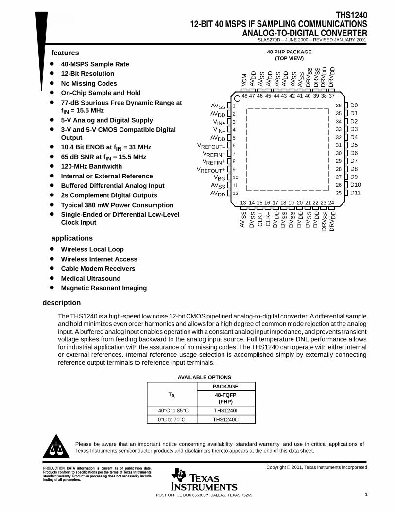
AVSSAVDDVIN+VIN–
AVDDVREFOUT–
VREFIN–VREFIN+
VREFOUT+VBG
AVSSAVDD
17 18 19 20
47 46 45 44 4348 42
V AV
CLK
+
40 39 3841
21 22 23 24
37
13
CLK
–
48 PHP PACKAGE(TOP VIEW)
CM D
DD
VD
DD
VS
SD
VS
SD
VD
DD
VS
SD
VD
DD
RV
SS
DR
VD
D
AV S
S
AV S
SA
V DD
AV S
S
DR
VS
S
AV
SS
DR
VS
S
AV D
D
DR
VD
DD
RV
DD
DV
SS
AV
SS
PRODUCTION DATA information is current as of publication date.Products conform to specifications per the terms of Texas Instrumentsstandard warranty. Production processing does not necessarily includetesting of all parameters.
Please be aware that an important notice concerning availability, standard warranty, and use in critical applications ofTexas Instruments semiconductor products and disclaimers thereto appears at the end of this data sheet.
THS124012-BIT 40 MSPS IF SAMPLING COMMUNICATIONSANALOG-TO-DIGITAL CONVERTERSLAS279D – JUNE 2000 – REVISED JANUARY 2001
2 POST OFFICE BOX 655303 • DALLAS, TEXAS 75265
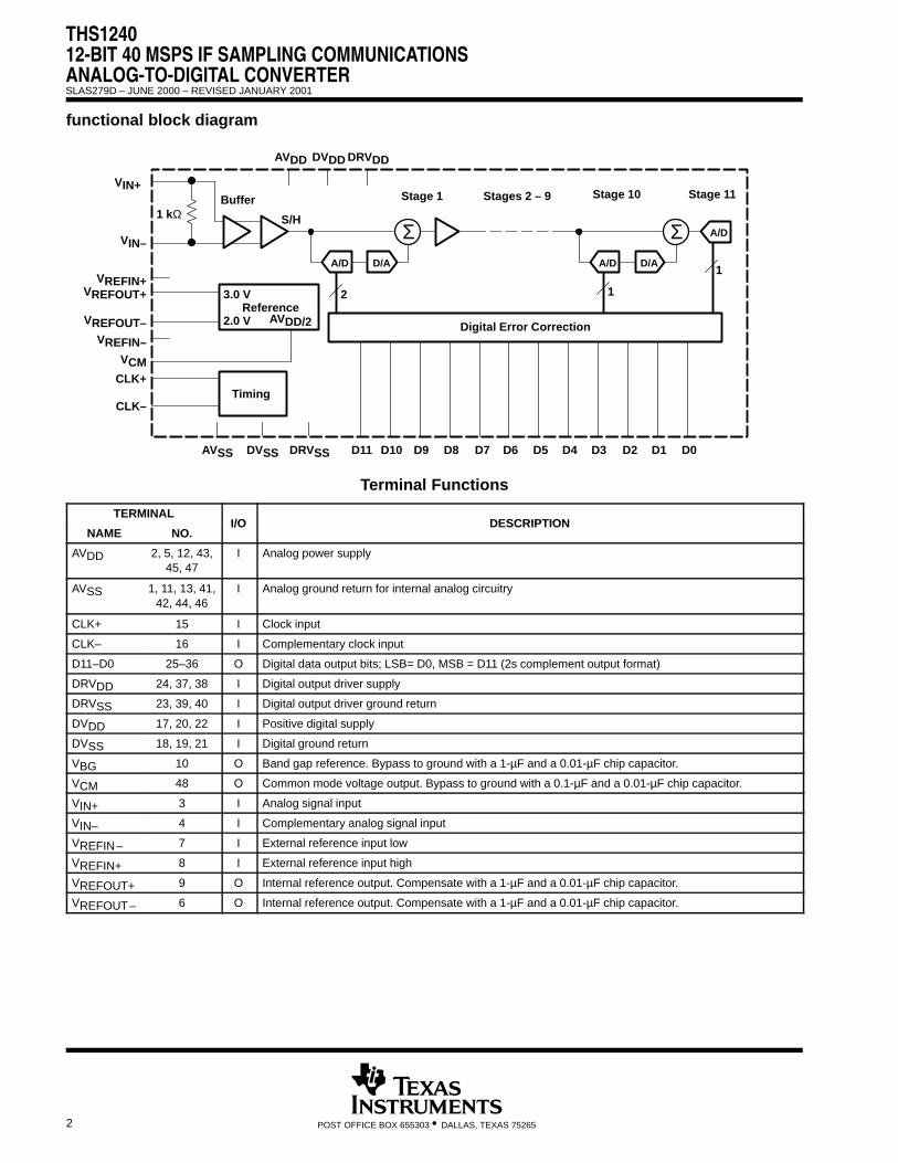
functional block diagram
Digital Error Correction
S/H
Stage 1 Stage 10
Reference3.0 V
2.0 V AVDD/2
Timing
VIN–
VREFOUT+
VCMCLK+
DVSS D9 D8 D7 D6 D5 D4 D3 D2 D1 D0
AVDD DVDD
D/A
Σ A/DΣD/AA/D A/D
VREFOUT–
VREFIN+
VREFIN–
CLK–
12
1
Buffer
DRVDD
AVSS DRVSS
Stages 2 – 9VIN+
Stage 11
D10D11
1 kΩ
Terminal Functions
TERMINALI/O DESCRIPTION
NAME NO.I/O DESCRIPTION
AVDD 2, 5, 12, 43,45, 47
I Analog power supply
AVSS 1, 11, 13, 41,42, 44, 46
I Analog ground return for internal analog circuitry
CLK+ 15 I Clock input
CLK– 16 I Complementary clock input
D11–D0 25–36 O Digital data output bits; LSB= D0, MSB = D11 (2s complement output format)
DRVDD 24, 37, 38 I Digital output driver supply
DRVSS 23, 39, 40 I Digital output driver ground return
DVDD 17, 20, 22 I Positive digital supply
DVSS 18, 19, 21 I Digital ground return
VBG 10 O Band gap reference. Bypass to ground with a 1-µF and a 0.01-µF chip capacitor.
VCM 48 O Common mode voltage output. Bypass to ground with a 0.1-µF and a 0.01-µF chip capacitor.
VIN+ 3 I Analog signal input
VIN– 4 I Complementary analog signal input
VREFIN– 7 I External reference input low
VREFIN+ 8 I External reference input high
VREFOUT+ 9 O Internal reference output. Compensate with a 1-µF and a 0.01-µF chip capacitor.
VREFOUT– 6 O Internal reference output. Compensate with a 1-µF and a 0.01-µF chip capacitor.

THS124012-BIT 40 MSPS IF SAMPLING COMMUNICATIONS
ANALOG-TO-DIGITAL CONVERTERSLAS279D – JUNE 2000 – REVISED JANUARY 2001
3POST OFFICE BOX 655303 • DALLAS, TEXAS 75265
functional description
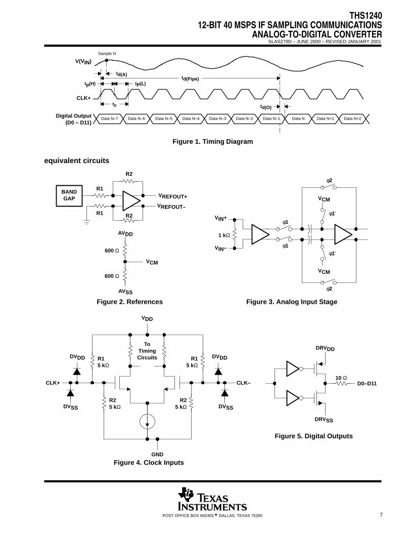
The THS1240 uses a differential pipeline architecture and assures no missing codes over the full operatingtemperature range. The device uses a 1 bit per stage architecture in order to achieve the highest possiblebandwidth. The differential analog inputs are terminated with a 1-kΩ resistor. The inputs are then fed to a unitygain buffer followed by the S/H (sample and hold) stage. This S/H stage is a switched capacitor operationalamplifier-based circuit, see Figure 3. The pipeline is a typical 1 bit per stage pipeline as shown in the functionalblock diagram. The digital output of the 12 stages is sent to a digital correction logic block which then outputsthe final 12 bits.
absolute maximum ratings over operating free-air temperature (unless otherwise noted)†
Supply voltage range: AVDD –0.5 V to 7 V. . . . . . . . . . . . . . . . . . . . . . . . . . . . . . . . . . . . . . . . . . . . . . . . . . . . . . . . DVDD –0.5 V to 7 V. . . . . . . . . . . . . . . . . . . . . . . . . . . . . . . . . . . . . . . . . . . . . . . . . . . . . . . . DRVDD –0.5 V to 7 V. . . . . . . . . . . . . . . . . . . . . . . . . . . . . . . . . . . . . . . . . . . . . . . . . . . . . .
Voltage between AVSS and DVSS and DRVSS –0.3 V to 0.5 V. . . . . . . . . . . . . . . . . . . . . . . . . . . . . . . . . . . . . . . . Voltage between DRVDD and DVDD –0.5 V to 5 V. . . . . . . . . . . . . . . . . . . . . . . . . . . . . . . . . . . . . . . . . . . . . . . . . . Voltage between AVDD and DVDD –0.5 V to 5 V. . . . . . . . . . . . . . . . . . . . . . . . . . . . . . . . . . . . . . . . . . . . . . . . . . . Digital data output –0.3 V to DVDD+0.3 V. . . . . . . . . . . . . . . . . . . . . . . . . . . . . . . . . . . . . . . . . . . . . . . . . . . . . . . . . . CLK peak input current, Ip(CLK) 20 mA. . . . . . . . . . . . . . . . . . . . . . . . . . . . . . . . . . . . . . . . . . . . . . . . . . . . . . . . . . . . Peak total input current (all inputs), Ip –30 mA. . . . . . . . . . . . . . . . . . . . . . . . . . . . . . . . . . . . . . . . . . . . . . . . . . . . . . Operating free-air temperature range, TA: THS1240C 0°C to 70°C. . . . . . . . . . . . . . . . . . . . . . . . . . . . . . . . . . . .
THS1240I –40°C to 85°C. . . . . . . . . . . . . . . . . . . . . . . . . . . . . . . . . . Storage temperature range – 65°C to 150°C. . . . . . . . . . . . . . . . . . . . . . . . . . . . . . . . . . . . . . . . . . . . . . . . . . . . . . . . Lead temperature 1,6 mm (1/16 inch) from the case for 10 seconds 260°C. . . . . . . . . . . . . . . . . . . . . . . . . . . .
† Stresses beyond those listed under absolute maximum ratings may cause permanent damage to the device. These are stress ratings only, andfunctional operation of the device at these or any other conditions beyond those indicated under recommended operating conditions is not implied.Exposure to absolute-maximum-rated conditions for extended periods may affect device reliability.
recommended operating conditions
MIN NOM MAX UNIT
Sample rate 1 40 MSPS
Analog supply voltage, AVDD 4.75 5 5.25 V
Digital supply voltage, DVDD 4.75 5 5.25 V
Digital output driver supply voltage, DRVDD 3 3.3 5.25 V
CLK + high level input voltage, VIH‡ 3.5 5 5.25 V
CLK + low-level input voltage, VIL‡ 0 1.5 V
CLK pulse-width high, tp(H) 10 12.5 ns
CLK pulse-width low, tp(L) 10 12.5 ns
Operating free air temperature range TATHS1240C 0 70
°COperating free-air temperature range, TATHS1240I –40 85
°C
‡ CLK– Input tied to ground with 0.01 µF capacitor for single-ended clock source.

THS124012-BIT 40 MSPS IF SAMPLING COMMUNICATIONSANALOG-TO-DIGITAL CONVERTERSLAS279D – JUNE 2000 – REVISED JANUARY 2001
4 POST OFFICE BOX 655303 • DALLAS, TEXAS 75265
electrical characteristics over recommended operating free-air temperature range, AVDD = DVDD = 5 V, DRVDD = 3.3 V, internal references, CLK = 40 MHz, single-ended clock sourceat 40 MHz with 50% duty cycle (unless otherwise noted)
dc accuracyPARAMETER TEST CONDITIONS MIN TYP† MAX UNIT
DNL Differential nonlinearity fIN = 15.5 MHz –1 ±0.6 1.25 LSB
No missing codes Assured
INL Integral nonlinearity fIN = 15.5 MHz ±2 LSB
EO Offset error V(VIN+) = V(VIN_) = VCM 14 70 mV
EG Gain error –7 –10 %FSR† All typical values are at TA = 25°C.
power supplyPARAMETER TEST CONDITIONS MIN TYP† MAX UNIT
I(AVDD) Analog supply current V(VIN) = (VCM) 73 110 mA
I(DVDD) Digital supply current V(VIN) = (VCM) 2 4 mA
I(DRVDD) Output driver supply current‡ V(VIN) = (VCM) 2 7 mA
PD Power dissipation V(VIN) = (VCM) 380 mW† All typical values are at TA = 25°C.‡ 15 pF load on digital outputs
referencePARAMETER TEST CONDITIONS MIN TYP† MAX UNIT
VREFOUT– Negative reference output voltage 1.9 2 2.1 V
VREFOUT+ Positive reference output voltage 2.9 3 3.1 V
VREFIN– External reference supplied 2 V
VREFIN+ External reference supplied 3 V
V(VCM) Common mode output voltage AVDD/2 V
I(VCM) Common mode output current 80 µA† All typical values are at TA = 25°C.
analog inputPARAMETER TEST CONDITIONS MIN TYP† MAX UNIT
RI Differential input resistance 1 kΩ
CI Differential input capacitance 4 pF
VI Analog input common mode range VCM ±0.05 V
VID Differential input voltage range 2 Vp-p
BW Analog input bandwidth (large signal) –3 dB 120 MHz† All typical values are at TA = 25°C.
digital outputsPARAMETER TEST CONDITIONS MIN TYP† MAX UNIT
VOH High-level output voltage IOH = –50 µA 0.8DRVDD V
VOL Low-level output voltage IOL = 50 µA 0.2DRVDD VDD
CL Output load capacitance 15 pF
† All typical values are at TA = 25°C.
THS124012-BIT 40 MSPS IF SAMPLING COMMUNICATIONS
ANALOG-TO-DIGITAL CONVERTERSLAS279D – JUNE 2000 – REVISED JANUARY 2001
5POST OFFICE BOX 655303 • DALLAS, TEXAS 75265
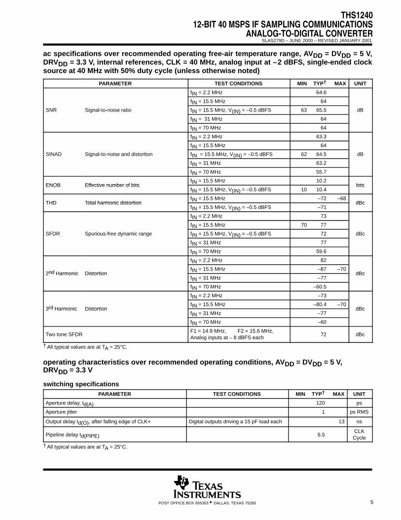
ac specifications over recommended operating free-air temperature range, AVDD = DVDD = 5 V,DRVDD = 3.3 V, internal references, CLK = 40 MHz, analog input at –2 dBFS, single-ended clocksource at 40 MHz with 50% duty cycle (unless otherwise noted)
PARAMETER TEST CONDITIONS MIN TYP† MAX UNIT
fIN = 2.2 MHz 64.6
fIN = 15.5 MHz 64
SNR Signal-to-noise ratio fIN = 15.5 MHz, V(IN) = –0.5 dBFS 63 65.5 dB
fIN = 31 MHz 64
fIN = 70 MHz 64
fIN = 2.2 MHz 63.3
fIN = 15.5 MHz 64
SINAD Signal-to-noise and distortion fIN = 15.5 MHz, V(IN) = –0.5 dBFS 62 64.5 dB
fIN = 31 MHz 63.2
fIN = 70 MHz 55.7
ENOB Effective number of bitsfIN = 15.5 MHz 10.2
bitsENOB Effective number of bitsfIN = 15.5 MHz, V(IN) = –0.5 dBFS 10 10.4
bits
THD Total harmonic distortionfIN = 15.5 MHz –72 –68
dBcTHD Total harmonic distortionfIN = 15.5 MHz, V(IN) = –0.5 dBFS –71
dBc
fIN = 2.2 MHz 73
fIN = 15.5 MHz 70 77
SFDR Spurious-free dynamic range fIN = 15.5 MHz, V(IN) = –0.5 dBFS 72 dBc
fIN = 31 MHz 77
fIN = 70 MHz 59.6
d
fIN = 2.2 MHz 82
2nd Harmonic DistortionfIN = 15.5 MHz –87 –70
dBc2nd Harmonic DistortionfIN = 31 MHz –77
dBc
fIN = 70 MHz –60.5
d
fIN = 2.2 MHz –73
3rd Harmonic DistortionfIN = 15.5 MHz –80.4 –70
dBc3rd Harmonic DistortionfIN = 31 MHz –77
dBc
fIN = 70 MHz –60
Two tone SFDRF1 = 14.9 MHz, F2 = 15.6 MHz,Analog inputs at – 8 dBFS each
72 dBc
† All typical values are at TA = 25°C.
operating characteristics over recommended operating conditions, AVDD = DVDD = 5 V, DRVDD = 3.3 V
switching specificationsPARAMETER TEST CONDITIONS MIN TYP† MAX UNIT
Aperture delay, td(A) 120 ps
Aperture jitter 1 ps RMS
Output delay td(O), after falling edge of CLK+ Digital outputs driving a 15 pF load each 13 ns
Pipeline delay td(PIPE) 6.5CLK
Cycle
† All typical values are at TA = 25°C.

THS124012-BIT 40 MSPS IF SAMPLING COMMUNICATIONSANALOG-TO-DIGITAL CONVERTERSLAS279D – JUNE 2000 – REVISED JANUARY 2001
6 POST OFFICE BOX 655303 • DALLAS, TEXAS 75265
definitions of specifications
analog bandwidthThe analog input frequency at which the spectral power of the fundamental frequency of a large input signalis reduced by 3 dB.
aperture delayThe delay between the 50% point of the rising edge of the clock and the instant at which the analog input issampled.
aperture uncertainity (jitter)The sample-to-sample variation in aperture delay
differential nonlinearityThe deviation of any output code from the ideal width of 1 LSB.
integral nonlinearityThe deviation of the transfer function from an end-point adjusted reference line measured in fractions of 1 LSB.Also the integral of the DNL curve.
clock pulse width/duty cyclePulse width high is the minimum amount of time that the clock pulse should be left in logic 1 state to achieverated performance; pulse width low is the minimum time clock pulse should be left in low state. At a given clockrate, these specs define acceptable clock duty cycles.
offset errorThe difference between the analog input voltage at which the ADC output changes from mid-scale to 1 LSBabove mid-scale, and the ideal voltage at which this transition should occur.
gain errorThe difference between the analog input voltage at which the ADC output changes from full-scale to 1 LSB belowfull scale, and the ideal voltage at which this transition should occur, minus the offset error
Gain Error 100%x2 VIN VIN_
2 V
@Code 4096
total harmonic distortionThe ratio of the power of the fundamental to a given harmonic component reported in dBc.
output delayThe delay between the 50% point of the falling edge of the clock and the time when all output data bits are withinvalid logic levels (not including pipeline delay).
signal-to-noise-and distortion (SINAD)When tested with a single tone, the ratio of the signal power to the sum of the power of all other spectralcomponents, excluding dc, referenced to full scale.
signal-to-noise ratio (SNR)When tested with a single tone, the ratio of the signal power to the sum of the power of all other power spectralcomponents, excluding dc and the first 9 harmonics, referenced to full scale.
effective number of bits (ENOB)For a sine wave, SINAD can be expressed in terms of the effective number of bits, using the following formula,
ENOB (SINAD 1.76)
6.02
spurious-free dynamic range (SFDR)The ratio of the signal power to the power of the worst spur, excluding dc. The worst spurious component mayor may not be a harmonic. The ratio is reported in dBc (that is, degrades as signal levels are lowered).
THS124012-BIT 40 MSPS IF SAMPLING COMMUNICATIONS
ANALOG-TO-DIGITAL CONVERTERSLAS279D – JUNE 2000 – REVISED JANUARY 2001
7POST OFFICE BOX 655303 • DALLAS, TEXAS 75265
V(VIN)
CLK+
Digital Output(D0 – D11)
Data N–7
tp(H) tP(L)
td(A)
Sample N
tc td(O)
td(Pipe)
Data N–6 Data N–5 Data N–4 Data N–3 Data N–2 Data N–1 Data N Data N+1 Data N+2
Figure 1. Timing Diagram
equivalent circuits
Figure 2. References Figure 3. Analog Input Stage
φ1′
φ1′
φ1
φ1
φ2
φ2
VCM
VCM
AVDD
VCM
AVSS
600 Ω
600 Ω
VREFOUT+
VREFOUT–
R2
R2
R1
R1
BANDGAP
VIN+
VIN–
1 kΩ
Figure 4. Clock Inputs
DVDD
CLK+
DVSS
R15 kΩ
R25 kΩ
GND
VDD
DVDDR15 kΩ
R25 kΩ
CLK–
DVSS
ToTimingCircuits
DRVSS
DRVDD
10 ΩD0–D11
Figure 5. Digital Outputs
THS124012-BIT 40 MSPS IF SAMPLING COMMUNICATIONSANALOG-TO-DIGITAL CONVERTERSLAS279D – JUNE 2000 – REVISED JANUARY 2001
8 POST OFFICE BOX 655303 • DALLAS, TEXAS 75265
APPLICATION INFORMATION
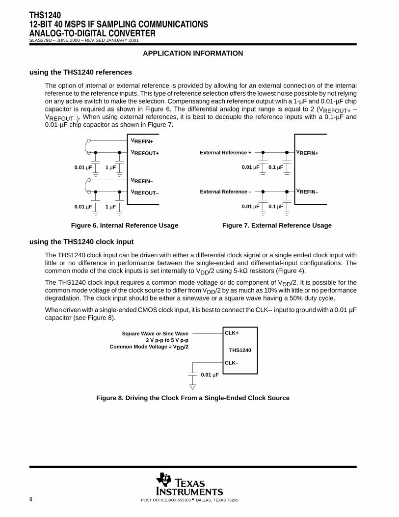
using the THS1240 references
The option of internal or external reference is provided by allowing for an external connection of the internalreference to the reference inputs. This type of reference selection offers the lowest noise possible by not relyingon any active switch to make the selection. Compensating each reference output with a 1-µF and 0.01-µF chipcapacitor is required as shown in Figure 6. The differential analog input range is equal to 2 (VREFOUT+ –VREFOUT–). When using external references, it is best to decouple the reference inputs with a 0.1-µF and0.01-µF chip capacitor as shown in Figure 7.
0.01 µF 1 µF
0.01 µF 1 µF
VREFIN+
VREFOUT+
VREFIN–
VREFOUT–
Figure 6. Internal Reference Usage Figure 7. External Reference Usage
0.01 µF 0.1 µF
0.01 µF 0.1 µF
External Reference + VREFIN+
VREFIN–External Reference –
using the THS1240 clock input
The THS1240 clock input can be driven with either a differential clock signal or a single ended clock input withlittle or no difference in performance between the single-ended and differential-input configurations. Thecommon mode of the clock inputs is set internally to VDD/2 using 5-kΩ resistors (Figure 4).
The THS1240 clock input requires a common mode voltage or dc component of VDD/2. It is possible for thecommon mode voltage of the clock source to differ from VDD/2 by as much as 10% with little or no performancedegradation. The clock input should be either a sinewave or a square wave having a 50% duty cycle.
When driven with a single-ended CMOS clock input, it is best to connect the CLK– input to ground with a 0.01 µFcapacitor (see Figure 8).
CLK+
THS1240
CLK–
Square Wave or Sine Wave2 V p-p to 5 V p-p
Common Mode Voltage = VDD/2
0.01 µF
Figure 8. Driving the Clock From a Single-Ended Clock Source

THS124012-BIT 40 MSPS IF SAMPLING COMMUNICATIONS
ANALOG-TO-DIGITAL CONVERTERSLAS279D – JUNE 2000 – REVISED JANUARY 2001
9POST OFFICE BOX 655303 • DALLAS, TEXAS 75265
APPLICATION INFORMATION
using the THS1240 clock input (continued)
If the dc component of the input clock differs from VDD/2 by more than 10%, it is best to connect the CLK+ inputto the clock source through a 0.01 µF capacitor. In this mode, the converter can operate with a clock having apeak-to-peak voltage of as little as 2 V with little or no performance degradation (see Figure 9).
CLK+
THS1240
CLK–
Square Wave or Sine Wave
2 V p-p to 5 V p-p
0.01 µF
0.01 µF
Figure 9. AC-Coupled Single-Ended Clock Input
The THS1240 clock input can also be driven differentially. If the common mode of the clock input is VDD/2, thenthe clock inputs can be driven directly (see Figure 10)
CLK+
THS1240
CLK–
Differential Square Wave orSine Wave 2 V p-p to 5 V p-p
Common Mode Voltage = VDD/2
Figure 10. Differential Clock Input
If the clock input is driven differentially with a clock signal having a common mode voltage that is different fromVDD/2, then it is best to connect both clock inputs to the differential input clock signal with 0.01 µF capacitors(see Figure 11). The differential input swing can vary between 2 V and 5 V with little or no performancedegradation.
CLK+
THS1240
CLK–
Differential Square Wave orSine Wave
2 V p-p to 5 V p-p0.01 µF
0.01 µF
Figure 11. AC-Coupled Differential Clock Input

THS124012-BIT 40 MSPS IF SAMPLING COMMUNICATIONSANALOG-TO-DIGITAL CONVERTERSLAS279D – JUNE 2000 – REVISED JANUARY 2001
10 POST OFFICE BOX 655303 • DALLAS, TEXAS 75265
APPLICATION INFORMATION
using the analog input
The THS1240 obtains optimum performance when the analog signal inputs are driven differentially. The circuitbelow shows the optimum configuration, see Figure 12. The signal is fed to the primary of an RF transformer.Since the input signal must be biased around the common mode voltage of the internal circuitry, the commonmode (VCM) reference from the THS1240 is connected to the center-tap of the secondary. To ensure a steadylow noise VCM reference, the best performance is obtained when the VCM output is connected to ground witha 0.1-µF and 0.01-µF low inductance capacitor.
R
VIN+
VCM
THS1240
0.01 µF 0.1 µF
Z0 = 50 Ω1:1
VIN–
50 ΩAC Signal Source
T1-1T
R0
50 Ω
Figure 12. Driving the THS1240 Analog Input With Impedance Matched Transmission Line
When it is necessary to buffer or apply a gain to the incoming analog signal, it is also possible to combine asingle-ended amplifier with an RF transformer as shown in Figure 13. For this application, a wide-band currentmode feedback amplifier such as the THS3001 is best. The noninverting input to the operational amplifier isterminated with a resistor having an impedance equal to the characteristic impedance of the trace that sourcesthe IF input signal. The single-ended output allows the use of standard passive filters between the amplifieroutput and the primary. In this case, the SFDR of the operational amplifier is not as critical as that of the A/Dconverter. While harmonics generated from within the A/D converter fold back into the first Nyquist zone,harmonics generated externally in the operational amplifier can be filtered out with passive filters.
VIN+
VIN–VCM
THS1240
0.1 µF 0.01 µF
_
+BPF
10 Ω
1 kΩ1 kΩ
RT
IF InputTHS3001
Impedance Ratio = 1:n
Figure 13. IF Input Buffered With THS3001 Operational Amplifier
THS124012-BIT 40 MSPS IF SAMPLING COMMUNICATIONS
ANALOG-TO-DIGITAL CONVERTERSLAS279D – JUNE 2000 – REVISED JANUARY 2001
11POST OFFICE BOX 655303 • DALLAS, TEXAS 75265
APPLICATION INFORMATION
digital outputs
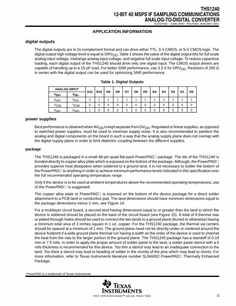
The digital outputs are in 2s complement format and can drive either TTL, 3-V CMOS, or 5-V CMOS logic. Thedigital output high voltage level is equal to DRVDD. Table 1 shows the value of the digital output bits for full scaleanalog input voltage, midrange analog input voltage, and negative full scale input voltage. To reduce capacitiveloading, each digital output of the THS1240 should drive only one digital input. The CMOS output drivers arecapable of handling up to a 15-pF load. For better SNR performance, use 3.3 V for DRVDD. Resistors of 200 Ωin series with the digital output can be used for optimizing SNR performance.
Table 1. Digital Outputs
ANALOG INPUTD11 D10 D9 D8 D7 D6 D5 D4 D3 D2 D1 D0
VIN+ VIN–D11 D10 D9 D8 D7 D6 D5 D4 D3 D2 D1 D0
Vref+ Vref– 0 1 1 1 1 1 1 1 1 1 1 1
VCM VCM 0 0 0 0 0 0 0 0 0 0 0 0
Vref– Vref+ 1 0 0 0 0 0 0 0 0 0 0 0
power supplies
Best performance is obtained when AVDD is kept separate from DVDD. Regulated or linear supplies, as opposedto switched power supplies, must be used to minimize supply noise. It is also recommended to partition theanalog and digital components on the board in such a way that the analog supply plane does not overlap withthe digital supply plane in order to limit dielectric coupling between the different supplies.
package
The THS1240 is packaged in a small 48-pin quad flat-pack PowerPAD package. The die of the THS1240 isbonded directly to copper alloy plate which is exposed on the bottom of the package. Although, the PowerPADprovides superior heat dissipation when soldered to a ground land, it is not necessary to solder the bottom ofthe PowerPAD to anything in order to achieve minimum performance levels indicated in this specification overthe full recommended operating temperature range.
Only if the device is to be used at ambient temperatures above the recommended operating temperatures, useof the PowerPAD is suggested.
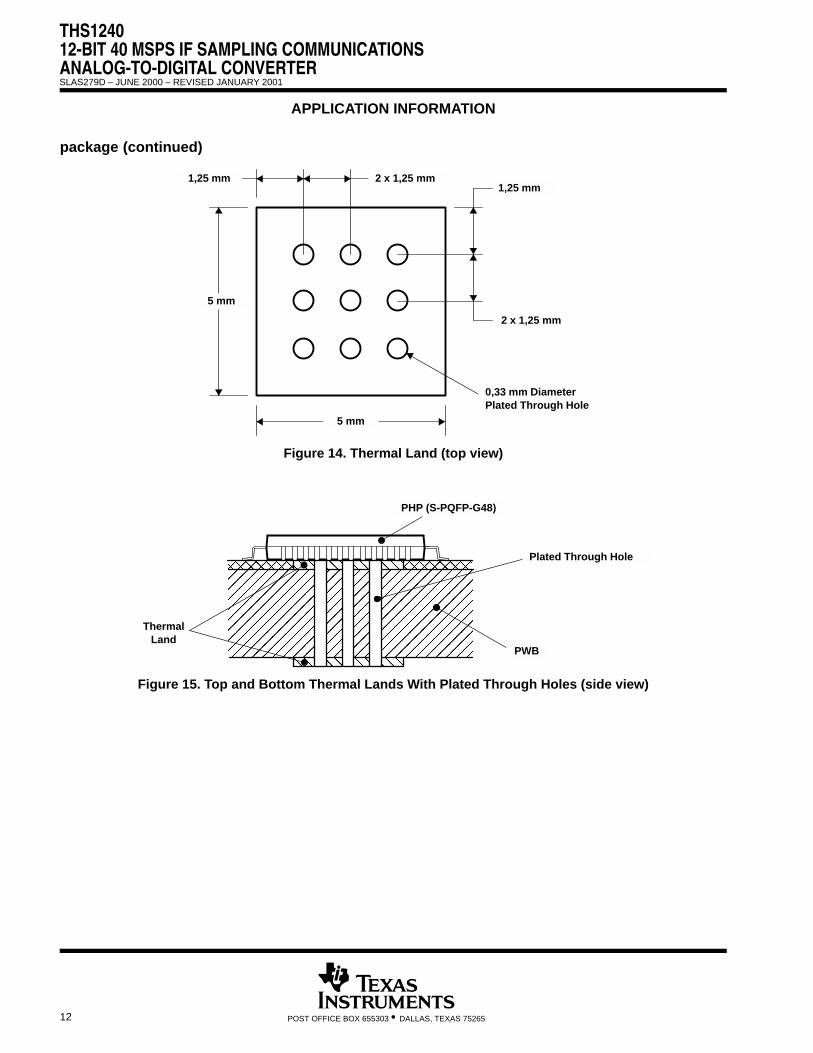
The copper alloy plate or PowerPAD is exposed on the bottom of the device package for a direct solderattachment to a PCB land or conductive pad. The land dimensions should have minimum dimensions equal tothe package dimensions minus 2 mm, see Figure 14.
For a multilayer circuit board, a second land having dimensions equal to or greater than the land to which thedevice is soldered should be placed on the back of the circuit board (see Figure 15). A total of 9 thermal viasor plated through-holes should be used to connect the two lands to a ground plane (buried or otherwise) havinga minimum total area of 3 inches square in 1 oz. copper. For the THS1240 package, the thermal via centersshould be spaced at a minimum of 1 mm. The ground plane need not be directly under or centered around thedevice footprint if a wide ground plane thermal run having a width on the order of the device is used to channelthe heat from the vias to the larger portion of the ground plane. The THS1240 package has a standoff of 0.19mm or 7.5 mils. In order to apply the proper amount of solder paste to the land, a solder paste stencil with a 6mils thickness is recommended for this device. Too thin a stencil may lead to an inadequate connection to theland. Too thick a stencil may lead to beading of solder in the vicinity of the pins which may lead to shorts. Formore information, refer to Texas Instruments literature number SLMA002 PowerPAD Thermally EnhancedPackage.
PowerPAD is a trademark of Texas Instruments.
THS124012-BIT 40 MSPS IF SAMPLING COMMUNICATIONSANALOG-TO-DIGITAL CONVERTERSLAS279D – JUNE 2000 – REVISED JANUARY 2001
12 POST OFFICE BOX 655303 • DALLAS, TEXAS 75265
APPLICATION INFORMATION
package (continued)
5 mm
5 mm
2 x 1,25 mm1,25 mm
2 x 1,25 mm
1,25 mm
0,33 mm DiameterPlated Through Hole
Figure 14. Thermal Land (top view)
ÎÎÎÎÎÎÎÎÎÎÎÎÎÎÎÎÎÎÎÎÎÎÎÎÎÎÎÎÎÎÎÎÎÎÎÎ
ÏÏÏÏÏÏÏÏÏÎÎÎÎÎÎÎÎÎÎÎÎÎÎÎÎÎÎÎÎÎÎÎÎÎÎÎÎÎÎÌÌ ÌÌ
ÌÌ ÌÌ
ÌÌÌÌ
ÌÌÌÌÎÎÎÎÎÎÎÎÎÎÎÎ
ÎÎÎÎÎÎÎÎÎÎÎÎ
ThermalLand
PWB
PHP (S-PQFP-G48)
Plated Through Hole
Figure 15. Top and Bottom Thermal Lands With Plated Through Holes (side view)
THS124012-BIT 40 MSPS IF SAMPLING COMMUNICATIONS
ANALOG-TO-DIGITAL CONVERTERSLAS279D – JUNE 2000 – REVISED JANUARY 2001
13POST OFFICE BOX 655303 • DALLAS, TEXAS 75265
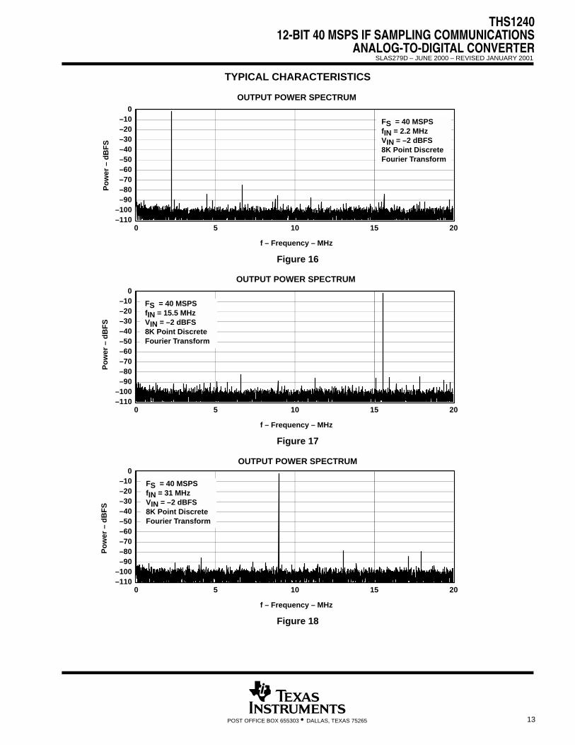
TYPICAL CHARACTERISTICS
–110–100–90–80–70–60–50–40–30–20–10
0
0 5 10 15 20
OUTPUT POWER SPECTRUM
f – Frequency – MHz
FS = 40 MSPSfIN = 2.2 MHzVIN = –2 dBFS8K Point DiscreteFourier Transform
Po
wer
– d
BF
S
Figure 16
–110–100–90–80–70–60–50–40–30–20–10
0
0 5 10 15 20
OUTPUT POWER SPECTRUM
f – Frequency – MHz
FS = 40 MSPSfIN = 15.5 MHzVIN = –2 dBFS8K Point DiscreteFourier Transform
Po
wer
– d
BF
S
Figure 17
–110–100–90–80–70–60–50–40–30–20–10
0
0 5 10 15 20
OUTPUT POWER SPECTRUM
f – Frequency – MHz
FS = 40 MSPSfIN = 31 MHzVIN = –2 dBFS8K Point DiscreteFourier Transform
Po
wer
– d
BF
S
Figure 18
THS124012-BIT 40 MSPS IF SAMPLING COMMUNICATIONSANALOG-TO-DIGITAL CONVERTERSLAS279D – JUNE 2000 – REVISED JANUARY 2001
14 POST OFFICE BOX 655303 • DALLAS, TEXAS 75265
TYPICAL CHARACTERISTICS
–110–100–90–80–70–60–50–40–30–20–10
0
0 5 10 15 20
OUTPUT POWER SPECTRUM
f – Frequency – MHz
FS = 40 MSPSfIN = 69 MHzVIN = –2 dBFS8K Point DiscreteFourier Transform
Po
wer
– d
BF
S
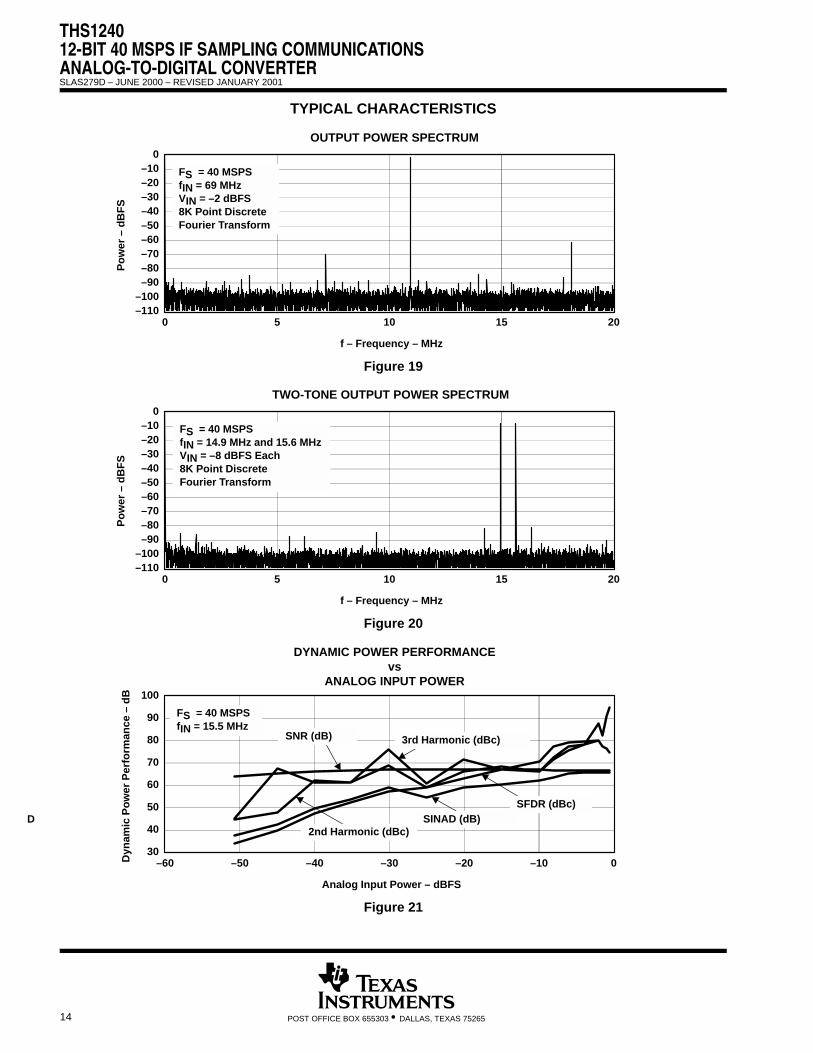
Figure 19
–110–100–90–80–70–60–50–40–30–20–10
0
0 5 10 15 20
TWO-TONE OUTPUT POWER SPECTRUM
f – Frequency – MHz
FS = 40 MSPSfIN = 14.9 MHz and 15.6 MHzVIN = –8 dBFS Each8K Point DiscreteFourier Transform
Po
wer
– d
BF
S
Figure 20
30
40
50
60
70
80
90
100
–60 –50 –40 –30 –20 –10 0
DYNAMIC POWER PERFORMANCEvs
ANALOG INPUT POWER
Analog Input Power – dBFS
FS = 40 MSPSfIN = 15.5 MHz
3rd Harmonic (dBc)
2nd Harmonic (dBc)SINAD (dB)
SFDR (dBc)
SNR (dB)
Dyn
amic
Po
wer
Per
form
ance
– d
B
D
Figure 21

THS124012-BIT 40 MSPS IF SAMPLING COMMUNICATIONS
ANALOG-TO-DIGITAL CONVERTERSLAS279D – JUNE 2000 – REVISED JANUARY 2001
15POST OFFICE BOX 655303 • DALLAS, TEXAS 75265
TYPICAL CHARACTERISTICS
30
40
50
60
70
80
90
100
0 10 20 30 40 50 60
DYNAMIC POWER PERFORMANCEvs
SAMPLING RATE
Sampling Rate – MSPS
fIN = 15.5 MHzVIN = –2 dBFS
3rd Harmonic (dBc)
3rd Harmonic (dBc)
2nd Harmonic (dBc)
SINAD (dB)SFDR (dBc)
SNR (dB)
Dyn
amic
Po
wer
Per
form
ance
– d
B
Figure 22
40
50
60
70
80
90
100
30 40 50 60 70
DYNAMIC POWER PERFORMANCEvs
DUTY CYCLE
Duty Cycle – %
fIN = 15.5 MHz VIN_ –2 dBFS
Dyn
amic
Po
wer
Per
form
ance
– d
B, d
Bc
SINAD (dB)
SFDR (dBc)SNR (dB)
Figure 23
THS124012-BIT 40 MSPS IF SAMPLING COMMUNICATIONSANALOG-TO-DIGITAL CONVERTERSLAS279D – JUNE 2000 – REVISED JANUARY 2001
16 POST OFFICE BOX 655303 • DALLAS, TEXAS 75265
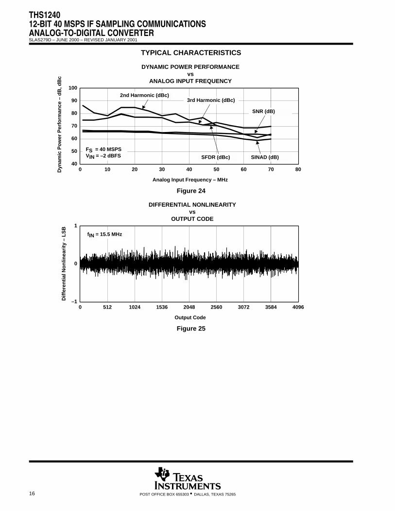
TYPICAL CHARACTERISTICS
40
50
60
70
80
90
100
0 10 20 30 40 50 60 70 80
DYNAMIC POWER PERFORMANCEvs
ANALOG INPUT FREQUENCY
Analog Input Frequency – MHz
FS = 40 MSPSVIN = –2 dBFS
3rd Harmonic (dBc)2nd Harmonic (dBc)
SINAD (dB)SFDR (dBc)
SNR (dB)
Dyn
amic
Po
wer
Per
form
ance
– d
B, d
Bc
Figure 24
–1
0
1
0 512 1024 1536 2048 2560 3072 3584 4096
DIFFERENTIAL NONLINEARITYvs
OUTPUT CODE
Output Code
fIN = 15.5 MHz
Dif
fere
nti
al N
on
linea
rity
– L
SB
Figure 25
THS124012-BIT 40 MSPS IF SAMPLING COMMUNICATIONS
ANALOG-TO-DIGITAL CONVERTERSLAS279D – JUNE 2000 – REVISED JANUARY 2001
17POST OFFICE BOX 655303 • DALLAS, TEXAS 75265
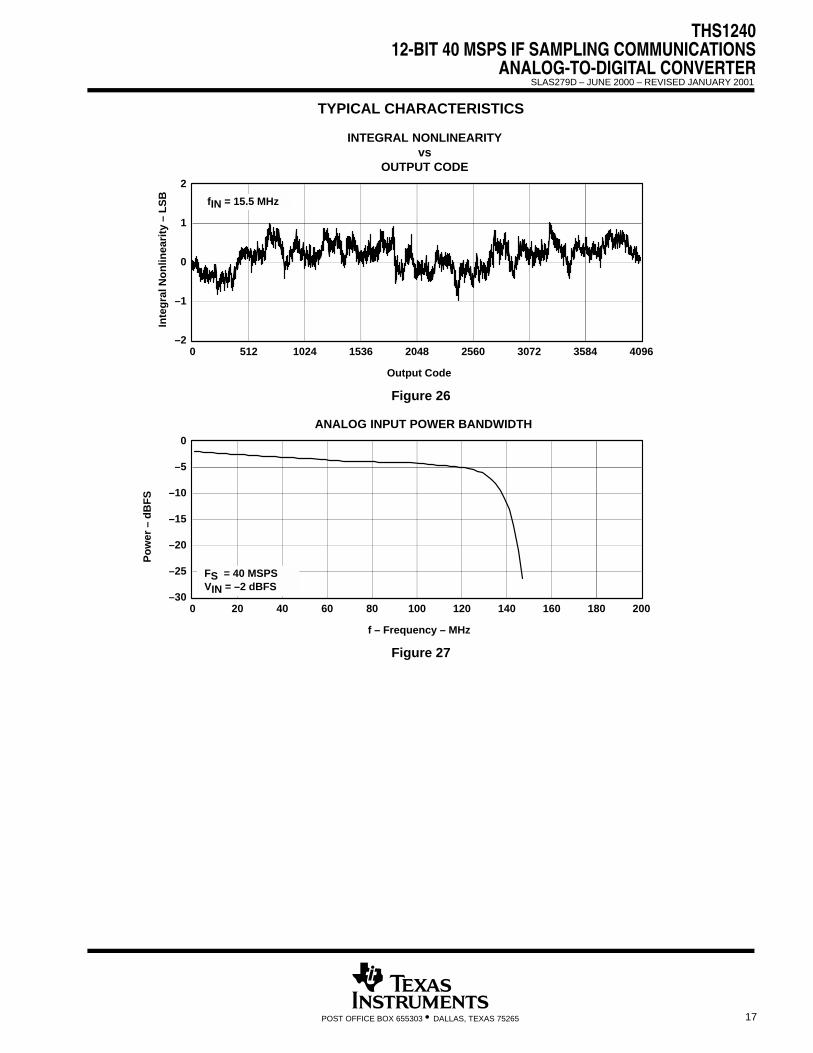
TYPICAL CHARACTERISTICS
–2
–1
0
1
2
0 512 1024 1536 2048 2560 3072 3584 4096
INTEGRAL NONLINEARITYvs
OUTPUT CODE
Output Code
fIN = 15.5 MHz
Inte
gra
l No
nlin
eari
ty –
LS
B
Figure 26
–30
–25
–20
–15
–10
–5
0
0 20 40 60 80 100 120 140 160 180 200
ANALOG INPUT POWER BANDWIDTH
f – Frequency – MHz
FS = 40 MSPSVIN = –2 dBFS
Po
wer
– d
BF
S
Figure 27
THS124012-BIT 40 MSPS IF SAMPLING COMMUNICATIONSANALOG-TO-DIGITAL CONVERTERSLAS279D – JUNE 2000 – REVISED JANUARY 2001
18 POST OFFICE BOX 655303 • DALLAS, TEXAS 75265
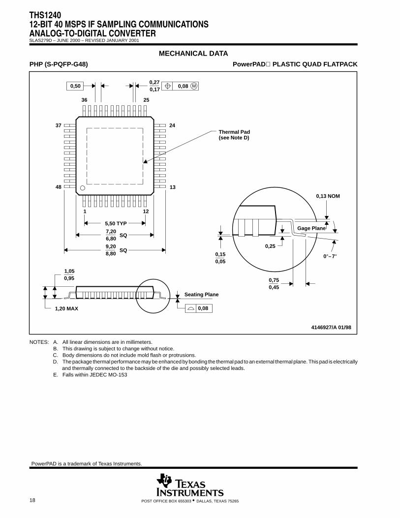
MECHANICAL DATAPHP (S-PQFP-G48) PowerPAD PLASTIC QUAD FLATPACK
Thermal Pad(see Note D)
Gage Plane
0,13 NOM
0,25
0,450,75
Seating Plane
4146927/A 01/98
0,170,27
24
25
13
12
SQ
36
37
7,206,80
48
1
5,50 TYP
SQ8,809,20
1,050,95
1,20 MAX
0,50 M0,08
0,08
0°–7°0,050,15
NOTES: A. All linear dimensions are in millimeters.B. This drawing is subject to change without notice.C. Body dimensions do not include mold flash or protrusions.D. The package thermal performance may be enhanced by bonding the thermal pad to an external thermal plane. This pad is electrically
and thermally connected to the backside of the die and possibly selected leads.E. Falls within JEDEC MO-153
PowerPAD is a trademark of Texas Instruments.

PACKAGING INFORMATION
Orderable Device Status (1) PackageType
PackageDrawing
Pins PackageQty
Eco Plan (2) Lead/Ball Finish MSL Peak Temp (3)
THS1240CPHP OBSOLETE HTQFP PHP 48 TBD Call TI Call TI
THS1240IPHP OBSOLETE HTQFP PHP 48 TBD Call TI Call TI
(1) The marketing status values are defined as follows:ACTIVE: Product device recommended for new designs.LIFEBUY: TI has announced that the device will be discontinued, and a lifetime-buy period is in effect.NRND: Not recommended for new designs. Device is in production to support existing customers, but TI does not recommend using this part ina new design.PREVIEW: Device has been announced but is not in production. Samples may or may not be available.OBSOLETE: TI has discontinued the production of the device.
(2) Eco Plan - The planned eco-friendly classification: Pb-Free (RoHS) or Green (RoHS & no Sb/Br) - please checkhttp://www.ti.com/productcontent for the latest availability information and additional product content details.TBD: The Pb-Free/Green conversion plan has not been defined.Pb-Free (RoHS): TI's terms "Lead-Free" or "Pb-Free" mean semiconductor products that are compatible with the current RoHS requirementsfor all 6 substances, including the requirement that lead not exceed 0.1% by weight in homogeneous materials. Where designed to be solderedat high temperatures, TI Pb-Free products are suitable for use in specified lead-free processes.Green (RoHS & no Sb/Br): TI defines "Green" to mean Pb-Free (RoHS compatible), and free of Bromine (Br) and Antimony (Sb) based flameretardants (Br or Sb do not exceed 0.1% by weight in homogeneous material)
(3) MSL, Peak Temp. -- The Moisture Sensitivity Level rating according to the JEDEC industry standard classifications, and peak soldertemperature.
Important Information and Disclaimer:The information provided on this page represents TI's knowledge and belief as of the date that it isprovided. TI bases its knowledge and belief on information provided by third parties, and makes no representation or warranty as to theaccuracy of such information. Efforts are underway to better integrate information from third parties. TI has taken and continues to takereasonable steps to provide representative and accurate information but may not have conducted destructive testing or chemical analysis onincoming materials and chemicals. TI and TI suppliers consider certain information to be proprietary, and thus CAS numbers and other limitedinformation may not be available for release.
In no event shall TI's liability arising out of such information exceed the total purchase price of the TI part(s) at issue in this document sold by TIto Customer on an annual basis.
PACKAGE OPTION ADDENDUM
www.ti.com 30-Mar-2005
Addendum-Page 1
IMPORTANT NOTICE
Texas Instruments Incorporated and its subsidiaries (TI) reserve the right to make corrections, modifications,enhancements, improvements, and other changes to its products and services at any time and to discontinueany product or service without notice. Customers should obtain the latest relevant information before placingorders and should verify that such information is current and complete. All products are sold subject to TI’s termsand conditions of sale supplied at the time of order acknowledgment.
TI warrants performance of its hardware products to the specifications applicable at the time of sale inaccordance with TI’s standard warranty. Testing and other quality control techniques are used to the extent TIdeems necessary to support this warranty. Except where mandated by government requirements, testing of allparameters of each product is not necessarily performed.
TI assumes no liability for applications assistance or customer product design. Customers are responsible fortheir products and applications using TI components. To minimize the risks associated with customer productsand applications, customers should provide adequate design and operating safeguards.
TI does not warrant or represent that any license, either express or implied, is granted under any TI patent right,copyright, mask work right, or other TI intellectual property right relating to any combination, machine, or processin which TI products or services are used. Information published by TI regarding third-party products or servicesdoes not constitute a license from TI to use such products or services or a warranty or endorsement thereof.Use of such information may require a license from a third party under the patents or other intellectual propertyof the third party, or a license from TI under the patents or other intellectual property of TI.
Reproduction of information in TI data books or data sheets is permissible only if reproduction is withoutalteration and is accompanied by all associated warranties, conditions, limitations, and notices. Reproductionof this information with alteration is an unfair and deceptive business practice. TI is not responsible or liable forsuch altered documentation.
Resale of TI products or services with statements different from or beyond the parameters stated by TI for thatproduct or service voids all express and any implied warranties for the associated TI product or service andis an unfair and deceptive business practice. TI is not responsible or liable for any such statements.
Following are URLs where you can obtain information on other Texas Instruments products and applicationsolutions:
Products Applications
Amplifiers amplifier.ti.com Audio www.ti.com/audio
Data Converters dataconverter.ti.com Automotive www.ti.com/automotive
DSP dsp.ti.com Broadband www.ti.com/broadband
Interface interface.ti.com Digital Control www.ti.com/digitalcontrol
Logic logic.ti.com Military www.ti.com/military
Power Mgmt power.ti.com Optical Networking www.ti.com/opticalnetwork
Microcontrollers microcontroller.ti.com Security www.ti.com/security
Telephony www.ti.com/telephony
Video & Imaging www.ti.com/video
Wireless www.ti.com/wireless
Mailing Address: Texas Instruments
Post Office Box 655303 Dallas, Texas 75265
Copyright 2005, Texas Instruments Incorporated